US12125953B2 - Method for manufacturing light emitting device, light emitting device, and light emitting module - Google Patents
Method for manufacturing light emitting device, light emitting device, and light emitting module Download PDFInfo
- Publication number
- US12125953B2 US12125953B2 US17/456,556 US202117456556A US12125953B2 US 12125953 B2 US12125953 B2 US 12125953B2 US 202117456556 A US202117456556 A US 202117456556A US 12125953 B2 US12125953 B2 US 12125953B2
- Authority
- US
- United States
- Prior art keywords
- light
- light emitting
- emitting device
- transmissive member
- recessed portion
- Prior art date
- Legal status (The legal status is an assumption and is not a legal conclusion. Google has not performed a legal analysis and makes no representation as to the accuracy of the status listed.)
- Active, expires
Links
- 238000004519 manufacturing process Methods 0.000 title claims abstract description 41
- 238000000034 method Methods 0.000 title claims abstract description 31
- 239000008393 encapsulating agent Substances 0.000 claims abstract description 60
- 230000008878 coupling Effects 0.000 claims abstract description 41
- 238000010168 coupling process Methods 0.000 claims abstract description 41
- 238000005859 coupling reaction Methods 0.000 claims abstract description 41
- 239000000758 substrate Substances 0.000 claims description 68
- 229920005989 resin Polymers 0.000 claims description 37
- 239000011347 resin Substances 0.000 claims description 37
- OAICVXFJPJFONN-UHFFFAOYSA-N Phosphorus Chemical compound [P] OAICVXFJPJFONN-UHFFFAOYSA-N 0.000 claims description 35
- 239000000463 material Substances 0.000 claims description 24
- 238000000748 compression moulding Methods 0.000 claims description 7
- 239000002245 particle Substances 0.000 claims description 7
- 238000001721 transfer moulding Methods 0.000 claims description 7
- 238000005520 cutting process Methods 0.000 claims description 5
- 238000005192 partition Methods 0.000 description 29
- 239000010410 layer Substances 0.000 description 24
- 239000004065 semiconductor Substances 0.000 description 21
- 238000009792 diffusion process Methods 0.000 description 20
- 230000003287 optical effect Effects 0.000 description 16
- 230000004048 modification Effects 0.000 description 13
- 238000012986 modification Methods 0.000 description 13
- 229910052751 metal Inorganic materials 0.000 description 10
- 239000002184 metal Substances 0.000 description 10
- 238000006243 chemical reaction Methods 0.000 description 8
- 238000009826 distribution Methods 0.000 description 8
- 230000010287 polarization Effects 0.000 description 7
- PCHJSUWPFVWCPO-UHFFFAOYSA-N gold Chemical compound [Au] PCHJSUWPFVWCPO-UHFFFAOYSA-N 0.000 description 6
- 229910052737 gold Inorganic materials 0.000 description 6
- 239000010931 gold Substances 0.000 description 6
- 229910052709 silver Inorganic materials 0.000 description 6
- 239000004332 silver Substances 0.000 description 6
- 229910052782 aluminium Inorganic materials 0.000 description 5
- 239000003795 chemical substances by application Substances 0.000 description 5
- 229920002050 silicone resin Polymers 0.000 description 5
- 239000004925 Acrylic resin Substances 0.000 description 4
- 229920000178 Acrylic resin Polymers 0.000 description 4
- BQCADISMDOOEFD-UHFFFAOYSA-N Silver Chemical compound [Ag] BQCADISMDOOEFD-UHFFFAOYSA-N 0.000 description 4
- 239000000945 filler Substances 0.000 description 4
- 239000004973 liquid crystal related substance Substances 0.000 description 4
- 239000000049 pigment Substances 0.000 description 4
- 229910045601 alloy Inorganic materials 0.000 description 3
- 239000000956 alloy Substances 0.000 description 3
- XAGFODPZIPBFFR-UHFFFAOYSA-N aluminium Chemical compound [Al] XAGFODPZIPBFFR-UHFFFAOYSA-N 0.000 description 3
- 239000003086 colorant Substances 0.000 description 3
- 239000003822 epoxy resin Substances 0.000 description 3
- 229910052733 gallium Inorganic materials 0.000 description 3
- 238000001579 optical reflectometry Methods 0.000 description 3
- 230000002093 peripheral effect Effects 0.000 description 3
- 239000011295 pitch Substances 0.000 description 3
- 229920005668 polycarbonate resin Polymers 0.000 description 3
- 239000004431 polycarbonate resin Substances 0.000 description 3
- 229920000647 polyepoxide Polymers 0.000 description 3
- RYGMFSIKBFXOCR-UHFFFAOYSA-N Copper Chemical compound [Cu] RYGMFSIKBFXOCR-UHFFFAOYSA-N 0.000 description 2
- XEEYBQQBJWHFJM-UHFFFAOYSA-N Iron Chemical compound [Fe] XEEYBQQBJWHFJM-UHFFFAOYSA-N 0.000 description 2
- PXHVJJICTQNCMI-UHFFFAOYSA-N Nickel Chemical compound [Ni] PXHVJJICTQNCMI-UHFFFAOYSA-N 0.000 description 2
- KDLHZDBZIXYQEI-UHFFFAOYSA-N Palladium Chemical compound [Pd] KDLHZDBZIXYQEI-UHFFFAOYSA-N 0.000 description 2
- 240000003380 Passiflora rubra Species 0.000 description 2
- GWEVSGVZZGPLCZ-UHFFFAOYSA-N Titan oxide Chemical compound O=[Ti]=O GWEVSGVZZGPLCZ-UHFFFAOYSA-N 0.000 description 2
- 229920001807 Urea-formaldehyde Polymers 0.000 description 2
- 238000004040 coloring Methods 0.000 description 2
- 229910052802 copper Inorganic materials 0.000 description 2
- 239000010949 copper Substances 0.000 description 2
- 239000002223 garnet Substances 0.000 description 2
- 238000002347 injection Methods 0.000 description 2
- 239000007924 injection Substances 0.000 description 2
- 150000004767 nitrides Chemical class 0.000 description 2
- 238000007747 plating Methods 0.000 description 2
- BASFCYQUMIYNBI-UHFFFAOYSA-N platinum Chemical compound [Pt] BASFCYQUMIYNBI-UHFFFAOYSA-N 0.000 description 2
- 239000000843 powder Substances 0.000 description 2
- 238000002310 reflectometry Methods 0.000 description 2
- 229920002803 thermoplastic polyurethane Polymers 0.000 description 2
- OGIDPMRJRNCKJF-UHFFFAOYSA-N titanium oxide Inorganic materials [Ti]=O OGIDPMRJRNCKJF-UHFFFAOYSA-N 0.000 description 2
- 229910003373 AgInS2 Inorganic materials 0.000 description 1
- 229910000906 Bronze Inorganic materials 0.000 description 1
- XPIIDKFHGDPTIY-UHFFFAOYSA-N F.F.F.P Chemical compound F.F.F.P XPIIDKFHGDPTIY-UHFFFAOYSA-N 0.000 description 1
- 229910002601 GaN Inorganic materials 0.000 description 1
- JMASRVWKEDWRBT-UHFFFAOYSA-N Gallium nitride Chemical compound [Ga]#N JMASRVWKEDWRBT-UHFFFAOYSA-N 0.000 description 1
- 229910001030 Iron–nickel alloy Inorganic materials 0.000 description 1
- 229910020440 K2SiF6 Inorganic materials 0.000 description 1
- 229910003564 SiAlON Inorganic materials 0.000 description 1
- VYPSYNLAJGMNEJ-UHFFFAOYSA-N Silicium dioxide Chemical compound O=[Si]=O VYPSYNLAJGMNEJ-UHFFFAOYSA-N 0.000 description 1
- 239000005084 Strontium aluminate Substances 0.000 description 1
- PQIJHIWFHSVPMH-UHFFFAOYSA-N [Cu].[Ag].[Sn] Chemical compound [Cu].[Ag].[Sn] PQIJHIWFHSVPMH-UHFFFAOYSA-N 0.000 description 1
- 239000000654 additive Substances 0.000 description 1
- 230000000996 additive effect Effects 0.000 description 1
- 239000000853 adhesive Substances 0.000 description 1
- 230000001070 adhesive effect Effects 0.000 description 1
- FNCIDSNKNZQJTJ-UHFFFAOYSA-N alumane;terbium Chemical compound [AlH3].[Tb] FNCIDSNKNZQJTJ-UHFFFAOYSA-N 0.000 description 1
- JNDMLEXHDPKVFC-UHFFFAOYSA-N aluminum;oxygen(2-);yttrium(3+) Chemical compound [O-2].[O-2].[O-2].[Al+3].[Y+3] JNDMLEXHDPKVFC-UHFFFAOYSA-N 0.000 description 1
- 229910002113 barium titanate Inorganic materials 0.000 description 1
- JRPBQTZRNDNNOP-UHFFFAOYSA-N barium titanate Chemical compound [Ba+2].[Ba+2].[O-][Ti]([O-])([O-])[O-] JRPBQTZRNDNNOP-UHFFFAOYSA-N 0.000 description 1
- 230000000903 blocking effect Effects 0.000 description 1
- 238000005219 brazing Methods 0.000 description 1
- 239000010974 bronze Substances 0.000 description 1
- UHYPYGJEEGLRJD-UHFFFAOYSA-N cadmium(2+);selenium(2-) Chemical compound [Se-2].[Cd+2] UHYPYGJEEGLRJD-UHFFFAOYSA-N 0.000 description 1
- GTDCAOYDHVNFCP-UHFFFAOYSA-N chloro(trihydroxy)silane Chemical compound O[Si](O)(O)Cl GTDCAOYDHVNFCP-UHFFFAOYSA-N 0.000 description 1
- 239000000470 constituent Substances 0.000 description 1
- KUNSUQLRTQLHQQ-UHFFFAOYSA-N copper tin Chemical compound [Cu].[Sn] KUNSUQLRTQLHQQ-UHFFFAOYSA-N 0.000 description 1
- 230000000694 effects Effects 0.000 description 1
- 230000005496 eutectics Effects 0.000 description 1
- 238000000605 extraction Methods 0.000 description 1
- YBMRDBCBODYGJE-UHFFFAOYSA-N germanium oxide Inorganic materials O=[Ge]=O YBMRDBCBODYGJE-UHFFFAOYSA-N 0.000 description 1
- JVPLOXQKFGYFMN-UHFFFAOYSA-N gold tin Chemical compound [Sn].[Au] JVPLOXQKFGYFMN-UHFFFAOYSA-N 0.000 description 1
- 230000005484 gravity Effects 0.000 description 1
- 229910052742 iron Inorganic materials 0.000 description 1
- 230000031700 light absorption Effects 0.000 description 1
- -1 lutetium aluminum Chemical compound 0.000 description 1
- 239000011159 matrix material Substances 0.000 description 1
- 238000002844 melting Methods 0.000 description 1
- 230000008018 melting Effects 0.000 description 1
- 238000000465 moulding Methods 0.000 description 1
- 229910052759 nickel Inorganic materials 0.000 description 1
- TWNQGVIAIRXVLR-UHFFFAOYSA-N oxo(oxoalumanyloxy)alumane Chemical compound O=[Al]O[Al]=O TWNQGVIAIRXVLR-UHFFFAOYSA-N 0.000 description 1
- 229910052763 palladium Inorganic materials 0.000 description 1
- 239000005011 phenolic resin Substances 0.000 description 1
- 229910052697 platinum Inorganic materials 0.000 description 1
- 229920013716 polyethylene resin Polymers 0.000 description 1
- 229920001721 polyimide Polymers 0.000 description 1
- 239000009719 polyimide resin Substances 0.000 description 1
- 229920005990 polystyrene resin Polymers 0.000 description 1
- 239000002096 quantum dot Substances 0.000 description 1
- 229910052594 sapphire Inorganic materials 0.000 description 1
- 239000010980 sapphire Substances 0.000 description 1
- 229910052814 silicon oxide Inorganic materials 0.000 description 1
- 239000002356 single layer Substances 0.000 description 1
- 229910000679 solder Inorganic materials 0.000 description 1
- 238000004544 sputter deposition Methods 0.000 description 1
- 238000006467 substitution reaction Methods 0.000 description 1
- 229920001187 thermosetting polymer Polymers 0.000 description 1
- 229910000969 tin-silver-copper Inorganic materials 0.000 description 1
- WFKWXMTUELFFGS-UHFFFAOYSA-N tungsten Chemical compound [W] WFKWXMTUELFFGS-UHFFFAOYSA-N 0.000 description 1
- 229910052721 tungsten Inorganic materials 0.000 description 1
- 239000010937 tungsten Substances 0.000 description 1
- 229910019901 yttrium aluminum garnet Inorganic materials 0.000 description 1
Images


Classifications
-
- H01L33/54—
-
- H01L33/005—
-
- H01L33/486—
-
- H01L33/56—
-
- H—ELECTRICITY
- H10—SEMICONDUCTOR DEVICES; ELECTRIC SOLID-STATE DEVICES NOT OTHERWISE PROVIDED FOR
- H10H—INORGANIC LIGHT-EMITTING SEMICONDUCTOR DEVICES HAVING POTENTIAL BARRIERS
- H10H20/00—Individual inorganic light-emitting semiconductor devices having potential barriers, e.g. light-emitting diodes [LED]
- H10H20/01—Manufacture or treatment
-
- H—ELECTRICITY
- H10—SEMICONDUCTOR DEVICES; ELECTRIC SOLID-STATE DEVICES NOT OTHERWISE PROVIDED FOR
- H10H—INORGANIC LIGHT-EMITTING SEMICONDUCTOR DEVICES HAVING POTENTIAL BARRIERS
- H10H20/00—Individual inorganic light-emitting semiconductor devices having potential barriers, e.g. light-emitting diodes [LED]
- H10H20/80—Constructional details
- H10H20/85—Packages
- H10H20/8506—Containers
-
- H—ELECTRICITY
- H10—SEMICONDUCTOR DEVICES; ELECTRIC SOLID-STATE DEVICES NOT OTHERWISE PROVIDED FOR
- H10H—INORGANIC LIGHT-EMITTING SEMICONDUCTOR DEVICES HAVING POTENTIAL BARRIERS
- H10H20/00—Individual inorganic light-emitting semiconductor devices having potential barriers, e.g. light-emitting diodes [LED]
- H10H20/80—Constructional details
- H10H20/85—Packages
- H10H20/852—Encapsulations
- H10H20/853—Encapsulations characterised by their shape
-
- H—ELECTRICITY
- H10—SEMICONDUCTOR DEVICES; ELECTRIC SOLID-STATE DEVICES NOT OTHERWISE PROVIDED FOR
- H10H—INORGANIC LIGHT-EMITTING SEMICONDUCTOR DEVICES HAVING POTENTIAL BARRIERS
- H10H20/00—Individual inorganic light-emitting semiconductor devices having potential barriers, e.g. light-emitting diodes [LED]
- H10H20/80—Constructional details
- H10H20/85—Packages
- H10H20/852—Encapsulations
- H10H20/854—Encapsulations characterised by their material, e.g. epoxy or silicone resins
-
- H—ELECTRICITY
- H10—SEMICONDUCTOR DEVICES; ELECTRIC SOLID-STATE DEVICES NOT OTHERWISE PROVIDED FOR
- H10H—INORGANIC LIGHT-EMITTING SEMICONDUCTOR DEVICES HAVING POTENTIAL BARRIERS
- H10H20/00—Individual inorganic light-emitting semiconductor devices having potential barriers, e.g. light-emitting diodes [LED]
- H10H20/80—Constructional details
- H10H20/85—Packages
- H10H20/855—Optical field-shaping means, e.g. lenses
-
- H01L2933/005—
-
- H—ELECTRICITY
- H10—SEMICONDUCTOR DEVICES; ELECTRIC SOLID-STATE DEVICES NOT OTHERWISE PROVIDED FOR
- H10H—INORGANIC LIGHT-EMITTING SEMICONDUCTOR DEVICES HAVING POTENTIAL BARRIERS
- H10H20/00—Individual inorganic light-emitting semiconductor devices having potential barriers, e.g. light-emitting diodes [LED]
- H10H20/01—Manufacture or treatment
- H10H20/036—Manufacture or treatment of packages
- H10H20/0362—Manufacture or treatment of packages of encapsulations
-
- H—ELECTRICITY
- H10—SEMICONDUCTOR DEVICES; ELECTRIC SOLID-STATE DEVICES NOT OTHERWISE PROVIDED FOR
- H10H—INORGANIC LIGHT-EMITTING SEMICONDUCTOR DEVICES HAVING POTENTIAL BARRIERS
- H10H20/00—Individual inorganic light-emitting semiconductor devices having potential barriers, e.g. light-emitting diodes [LED]
- H10H20/01—Manufacture or treatment
- H10H20/036—Manufacture or treatment of packages
- H10H20/0363—Manufacture or treatment of packages of optical field-shaping means
-
- H—ELECTRICITY
- H10—SEMICONDUCTOR DEVICES; ELECTRIC SOLID-STATE DEVICES NOT OTHERWISE PROVIDED FOR
- H10H—INORGANIC LIGHT-EMITTING SEMICONDUCTOR DEVICES HAVING POTENTIAL BARRIERS
- H10H20/00—Individual inorganic light-emitting semiconductor devices having potential barriers, e.g. light-emitting diodes [LED]
- H10H20/80—Constructional details
- H10H20/85—Packages
- H10H20/851—Wavelength conversion means
- H10H20/8514—Wavelength conversion means characterised by their shape, e.g. plate or foil
-
- H—ELECTRICITY
- H10—SEMICONDUCTOR DEVICES; ELECTRIC SOLID-STATE DEVICES NOT OTHERWISE PROVIDED FOR
- H10H—INORGANIC LIGHT-EMITTING SEMICONDUCTOR DEVICES HAVING POTENTIAL BARRIERS
- H10H20/00—Individual inorganic light-emitting semiconductor devices having potential barriers, e.g. light-emitting diodes [LED]
- H10H20/80—Constructional details
- H10H20/85—Packages
- H10H20/857—Interconnections, e.g. lead-frames, bond wires or solder balls
Definitions
- the present disclosure relates to a method for manufacturing a light emitting device, a light emitting device, and a light emitting module.
- a light emitting device including a light emitting element such as a light emitting diode is known (See, for example, Japanese Patent Publication No. 2013-106047).
- the light emitting device includes a reflective first body that is disposed on a plurality of leads and has a region open in a predetermined region among upper surface regions of the plurality of leads, a light transmissive second body that has a first opening corresponding to the open region of the first body and is disposed on an upper surface of the first body, a light emitting chip disposed on at least one of the plurality of lead frames exposed from the first opening of the second body, and a first resin layer that is disposed in the first opening of the second body and covers the light emitting chip.
- a reflective first body that is disposed on a plurality of leads and has a region open in a predetermined region among upper surface regions of the plurality of leads
- a light transmissive second body that has a first opening corresponding to the open region of the first body and is disposed on an upper surface
- An exemplary object of the present disclosure is to provide a method for manufacturing a light emitting device that affords a thinner light emitting device, such a light emitting device, and a light emitting module.
- a method for manufacturing a light emitting device includes: providing an intermediate member including: a support member including: a plurality of housing portions, at least one of the housing portions having a first recessed portion that has a lateral wall and a bottom surface, and a coupling portion located between the at least one of the housing portions and an adjacent one of the housing portions and having a height lower than a height of the lateral wall with reference to the bottom surface of the first recessed portion, a light source mounted on the bottom surface of the first recessed portion, and an encapsulant disposed in the first recessed portion and covering the light source; and forming a first light-transmissive member that continuously covers at least one of the housing portions and the coupling portion.
- a surface of the first light-transmissive member has an inclined surface, wherein a height of the inclined surface above the coupling portion is lower than a height of the inclined surface above the at least one of the housing portions with reference to the bottom surface of the first recessed portion.
- a light emitting device includes: a light source; an encapsulant that covers a light emitting surface and a lateral surface of the light source; and a light-transmissive member that covers an upper surface and a lateral surface of the encapsulant.
- the light-transmissive member has an octagon shape in a plan view. All interior angles of the octagonal shape are less than 180 degrees, and at least one of the interior angles is different from another of the interior angles.
- a light emitting module includes: a substrate on which the light emitting device according to an embodiment of the present disclosure; and a partition member that is disposed on the same side of the substrate where the light emitting device is disposed, and includes a wall portion surrounding the light emitting device in a plan view.
- a method for manufacturing a light emitting device that affords a thinner light emitting device can be provided, such a light emitting device, and a light emitting module.
- FIG. 1 is a schematic plan view exemplifying a light emitting device according to a first embodiment of the present disclosure.
- FIG. 2 is a schematic cross-sectional view taken along line II-II in FIG. 1 exemplifying the light emitting device according to the first embodiment.
- FIG. 3 is a schematic cross-sectional view ( 1 ) exemplifying a manufacturing step of the light emitting device according to the first embodiment.
- FIG. 4 is a schematic plan view ( 1 ) exemplifying a manufacturing step of the light emitting device according to the first embodiment.
- FIG. 5 is a schematic cross-sectional view ( 2 ) exemplifying a manufacturing step of the light emitting device according to the first embodiment.
- FIG. 6 is a schematic plan view ( 2 ) exemplifying a manufacturing step of the light emitting device according to the first embodiment.
- FIG. 7 is a schematic cross-sectional view ( 3 ) exemplifying a manufacturing step of the light emitting device according to the first embodiment.
- FIG. 8 is a schematic cross-sectional view ( 4 ) exemplifying a manufacturing step of the light emitting device according to the first embodiment.
- FIG. 9 is a schematic cross-sectional view ( 5 ) exemplifying a manufacturing step of the light emitting device according to the first embodiment.
- FIG. 11 is a schematic plan view ( 1 ) exemplifying a planar light source comprising a light emitting device 1 .
- FIG. 12 is a schematic plan view ( 2 ) exemplifying a planar light source comprising the light emitting device 1 .
- FIG. 13 is a schematic plan view illustrating a specific example of a planar light source comprising the light emitting device 1 .
- FIG. 14 is a schematic partial cross-sectional view taken along line XIV-XIV in FIG. 13 illustrating a specific example of the planar light source comprising the light emitting device 1 .
- FIG. 15 is a schematic cross-sectional view ( 1 ) exemplifying a light emitting device according to a first modification example of the first embodiment.
- FIG. 16 is a schematic cross-sectional view ( 2 ) exemplifying a light emitting device according to the first modification example of the first embodiment.
- FIG. 17 is a schematic cross-sectional view ( 3 ) exemplifying a light emitting device according to the first modification example of the first embodiment.
- FIG. 18 is a schematic cross-sectional view ( 4 ) exemplifying a light emitting device according to the first modification example of the first embodiment.
- FIG. 19 is a schematic plan view exemplifying a light emitting device according to a second embodiment of the present disclosure.
- FIG. 20 is a schematic cross-sectional view taken along line II-II in FIG. 19 exemplifying the light emitting device according to the second embodiment.
- FIG. 21 is a schematic plan view ( 1 ) for describing the light emitting device according to the second embodiment.
- FIG. 22 is a schematic plan view ( 2 ) for describing the light emitting device according to the second embodiment.
- FIG. 23 is a plan view schematically illustrating a direction of light from a light source using an arrow.
- FIG. 1 is a schematic plan view exemplifying a light emitting device according to a first embodiment.
- FIG. 2 is a schematic cross-sectional view taken along line II-II in FIG. 1 exemplifying the light emitting device according to the first embodiment.
- a light emitting device 1 includes a substrate 10 , a light source 20 , an encapsulant 30 , and a light-transmissive member 40 .
- the substrate 10 is a member provided as necessary, and is not an essential component of the light emitting device 1 .
- the light source 20 is mounted on an upper surface 10 a side of the substrate 10 .
- the light source 20 includes an upper surface 20 a and at least a lateral surface 20 c .
- Light from the light source 20 is emitted from the upper surface 20 a , and is also emitted from the lateral surface 20 c .
- the encapsulant 30 is provided on the upper surface 10 a side of the substrate 10 , and covers the upper surface 20 a and the lateral surface 20 c of the light source 20 .
- the light-transmissive member 40 is provided on the upper surface 10 a side of the substrate 10 , covers the encapsulant 30 , and is located above the upper surface 20 a of the light source 20 and to the lateral side of the lateral surface 20 c .
- light from the light source 20 is emitted in an upper direction and a lateral direction of the light-transmissive member 40 through the encapsulant 30 and the light-transmissive member 40 .
- Each element constituting the light emitting device 1 will be described below in detail.
- the substrate 10 includes a pair of leads 11 and an insulating member 12 . Most of a periphery of each of the leads 11 is embedded with the insulating member 12 , and a part of the periphery is exposed from the insulating member 12 . Further, an upper surface and a lower surface of each of the leads 11 are exposed from the insulating member 12 . For example, the upper surface of each of the leads 11 and an upper surface of the insulating member 12 are in the same plane, and the lower surface of each of the leads 11 and a lower surface of the insulating member 12 are in the same plane. The lower surface of each of the leads 11 is, for example, an external connection terminal.
- a plate-like body formed of at least one kind of metal selected from copper, aluminum, gold, silver, tungsten, iron, and nickel, an alloy such as an iron-nickel alloy and phosphor bronze, and a clad material can be used.
- Silver, aluminum, gold, an alloy thereof, or a film of metal (for example, a film formed by plating) comprising silver may be formed on a surface of the lead 11 in order to efficiently extract light from the light source 20 .
- the film of metal formed on the surface of the lead 11 may be a single layer film or a multilayer film.
- the material of the insulating member 12 preferably has good light reflectivity, and examples of the material include a white resin in which white powder being an additive that reflects light, a filler, a diffusion agent, a reflective material, and the like is added to a transparent resin.
- the insulating member 12 is preferably a silicone resin containing inorganic white powder such as titanium oxide. When the insulating member 12 includes a resin containing a light reflective material, exit of light to the substrate side is suppressed.
- the insulating member 12 preferably has reflectivity equal to or greater than 60%, more preferably reflectivity equal to or greater than 90%, with respect to light emitted from the light source 20 .
- the light source 20 is, for example, a light emitting element.
- a light emitting device including a light emitting element and another member may be used as the light source 20 .
- a light emitting element having the upper surface 20 a and the lateral surface 20 c is exemplified as the light source 20 .
- the light source 20 has, for example, a rectangle shape in a plan view.
- the light source 20 includes, for example, a pair of electrodes 20 t on the upper surface 20 a side, and the pair of electrodes 20 t of the light source 20 and the pair of leads 11 of the substrate 10 are electrically connected by metal wires 25 .
- a material of the metal wire 25 include a metal such as gold, silver, copper, platinum, and aluminum, and an alloy thereof, but gold having good thermal conductivity and the like is preferably used in particular.
- the thickness of the metal wire 25 can be appropriately selected depending on the purpose and application.
- the light emitting element includes, for example, an element substrate such as sapphire or gallium nitride, and a semiconductor layered body.
- the semiconductor layered body includes an n-type semiconductor layer, a p-type semiconductor layer, an active layer sandwiched between the n-type semiconductor layer and the p-type semiconductor layer, and electrodes electrically connected to the n-type semiconductor layer and the p-type semiconductor layer.
- the semiconductor layered body may include a nitride-based semiconductor (In X Al Y Ga 1-X-Y N, 0 ⁇ X, 0 ⁇ Y, and X+Y ⁇ 1) that can emit light in an ultraviolet region to a visible region.
- the semiconductor layered body can include at least one light emitting layer that can emit light in the ultraviolet region to the visible region as described above.
- the semiconductor layered body can include a light emitting layer that can emit light in one light emission color or one light emission wavelength between the n-type semiconductor layer and the p-type semiconductor layer.
- the light emitting layer may have a double heterojunction structure, a single quantum well structure (SQW), or a multiple quantum well structure (MQW).
- the semiconductor layered body can also include a plurality of light emitting layers.
- the semiconductor layered body may have a structure including a plurality of light emitting layers between the n-type semiconductor layer and the p-type semiconductor layer, or may have a structure in which the n-type semiconductor layer, the light emitting layer, and the p-type semiconductor layer are sequentially repeated multiple times.
- the plurality of light emitting layers may include active layers having light emission colors different from each other or light emission wavelengths different from each other, or may include active layers having the same light emission color each other or the same light emission wavelength each other. Note that the same light emission color may have a variation in a range to be considered as the same light emission color for use, for example, approximately several nm at a main wavelength.
- a combination of light emission colors or light emission wavelengths can be appropriately selected.
- examples of a combination of light emission colors include blue light and blue light, green light and green light, red light and red light, ultraviolet light and ultraviolet light, blue light and green light, blue light and red light, and green light and red light.
- the encapsulant 30 has a rectangle shape larger than that of the light source 20 in plan view.
- the center of the encapsulant 30 preferably matches an optical axis of the light source 20 in plan view.
- the optical axis of the light source 20 is defined as a line that passes through the center of the upper surface 20 a of the light source 20 and perpendicularly intersects the upper surface 20 a .
- each vertex of the rectangle shape of the encapsulant 30 is located on, for example, an extended line of a diagonal line of the rectangle shape of the light source 20 .
- the light source 20 and the encapsulant 30 have, for example, similar shapes.
- a resin having good heat resistance, weather resistance, and light resistance is preferably used as the encapsulant 30 .
- a resin include a silicone resin, a modified silicone resin, an epoxy resin, a modified epoxy resin, a urea resin, a phenol resin, an acrylic resin, a urethane resin, a fluororesin, or a resin containing two or more kinds of these resins.
- the encapsulant 30 can be mixed with at least one kind selected from the group consisting of a filler, a diffusion agent, a pigment, a fluorescent material, and a reflective material in order to impart a predetermined function.
- a filler e.g., a filler, a diffusion agent, a pigment, a fluorescent material, and a reflective material.
- Barium titanate, titanium oxide, aluminum oxide, silicon oxide, and the like can be suitably used as the diffusion agent.
- the encapsulant 30 may contain an organic or inorganic coloring dye or coloring pigment for the purpose of blocking a wavelength except for a desired wavelength. Further, the encapsulant 30 may contain a phosphor.
- the encapsulant 30 functions as a wavelength conversion member when the encapsulant 30 contains the phosphor.
- the wavelength conversion member absorbs at least a part of light emitted from the light source 20 , and emits light having a wavelength different from a wavelength of the light emitted from the light source 20 .
- the wavelength conversion member converts a wavelength of a part of blue light from the light source 20 , and emits yellow light. According to such a configuration, white light is obtained by mixing blue light that has passed through the wavelength conversion member and yellow light emitted from the wavelength conversion member.
- Phosphors known in the art may be used. Specifically, an yttrium aluminum garnet based phosphor (for example, Y 3 (Al,Ga) 5 O 12 :Ce), a lutetium aluminum garnet based phosphor (for example, Lu 3 (Al,Ga) 5 O 12 :Ce), a terbium aluminum garnet based phosphor (for example, Tb 3 (Al,Ga) 5 O 12 :Ce), a CCA based phosphor (for example, Ca 10 (PO 4 ) 6 Cl 2 :Eu), an SAE based phosphor (for example, Sr 4 Al 14 O 25 :Eu), a chlorosilicate based phosphor (for example, Ca 8 MgSi 4 O 16 Cl 2 :Eu), a ⁇ -SiALON based phosphor (for example, (Si,Al) 3 (O,N) 4 :Eu), an ⁇ based SiAlON phospho
- the planar shape of the encapsulant 30 may be various shapes such as a rectangular shape and a circular shape, but the encapsulant 30 preferably has a rectangular shape.
- the planar shape of the light source 20 is a rectangular shape
- the planar shape of the encapsulant 30 is also a rectangular shape larger than the planar shape of the light source, a distance in which light passes through the encapsulant 30 in a diagonal line direction of the light source and the distance in a direction perpendicular to each one side can be set substantially the same.
- the color of light having a wavelength converted by the phosphor in the diagonal line direction is substantially the same as that in the direction perpendicular to one side, and unevenness in color of the light emitting device 1 can be reduced.
- a resin having good heat resistance, weather resistance, and hardness is preferably used as the light-transmissive member 40 .
- a resin include an epoxy resin, a silicone resin, a modified silicone resin, a urea resin, a urethane resin, an acrylic resin, a polycarbonate resin, or a polyimide resin, or a resin containing two or more kinds of these resins.
- the light-transmissive member 40 can be mixed with at least one kind selected from the group consisting of a filler, a diffusion agent, a pigment, and a reflective material in order to impart a predetermined function.
- the light-transmissive member 40 has, for example, a rectangle shape in plan view.
- the light-transmissive member 40 has, for example, a square shape in plan view.
- the center of the light-transmissive member 40 preferably matches the optical axis of the light source 20 in plan view.
- four vertices of the square shape of the light-transmissive member 40 are located on, for example, extended line of both the diagonal line of the rectangle shape of the light source 20 and the diagonal line of the encapsulant 30 .
- the light source 20 , the encapsulant 30 , and the light-transmissive member 40 have, for example, similar shapes.
- the light-transmissive member 40 is circular in plan view
- directivity in each direction is uniform.
- the light-transmissive member 40 has a square shape in plan view
- directivity in the diagonal line direction of the square can be improved, and intensity of light in the diagonal line direction can be set higher than intensity of light in the direction perpendicular to the center of each side of the square and the like. This characteristic is suitable when a reflector having a rectangular shape in plan view is located around the light emitting device 1 , for example.
- a distance from the center of the light emitting device 1 to the four corners of the reflector having the rectangular shape in plan view is longer than a distance to another portion, and thus the four corners of the reflector tend to be dark.
- the four corners of the reflector are dark, unevenness in brightness will occur.
- the light-transmissive member 40 is a square in plan view in the light emitting device 1 , the directivity in the diagonal line direction of the square is improved, and the intensity of light in the diagonal line direction is set higher than the intensity of light in the direction perpendicular to the center of each side of the square and the like.
- darkness at the four corners of the reflector having the rectangular shape in plan view can be suppressed, and unevenness in brightness can be reduced.
- the light-transmissive member 40 is not limited to having a square shape in plan view, and may be a polygon having an additional corner added to a square.
- examples include an octagon in which the center of each side of the square illustrated in FIG. 1 is equally shifted to the outside of the square in the direction perpendicular to each side.
- the intensity of light that travels in the direction to the four corners of the reflector having the rectangular shape in plan view can be increased, and thus darkness at the four corners of the reflector can be suppressed, and unevenness in brightness can be reduced.
- a surface of the light-transmissive member 40 has an inclined surface 40 a having a height on a peripheral end side lower than a height on a center side with reference to the lower surface of the light source 20 .
- the inclined surface 40 a is provided in, for example, an annular shape outside the encapsulant 30 in plan view.
- light from the light source 20 is refracted at the inclined surface 40 a , and is emitted in the lateral direction.
- the inclined surface 40 a may be formed in a curved shape in a cross-sectional view, but is preferably formed linearly in the cross-sectional view.
- the surface of the light-transmissive member 40 has a recessed portion 40 x (i.e., second recessed portion) recessed toward the light source 20 side in a region overlapping the encapsulant 30 in plan view.
- the recessed portion 40 x preferably has a deepest portion located at a position at the center of the recessed portion 40 x in plan view. Lateral surfaces of the recessed portion 40 x are preferably axisymmetric in a cross section including a central axis that passes through the center of the recessed portion 40 x .
- the recessed portion 40 x defines, for example, a cone shape or a frustum shape.
- the recessed portion 40 x has, for example, a rectangle shape in plan view.
- the recessed portion 40 x defines, for example, a quadrangular pyramid shape or a truncated pyramid shape.
- the center of the recessed portion 40 x preferably matches the optical axis of the light source 20 in plan view.
- the recessed portion 40 x controls an emission direction of light by using refraction of light at an interface between environments inside and outside the light-transmissive member 40 .
- the recessed portion 40 x has inclined lateral surfaces as in the case of the cone shape or the frustum shape, light reflected by the interface between environments inside and outside the light-transmissive member 40 diffuses in a wider range in the light-transmissive member 40 , and travels to the substrate 10 side.
- the light from the light source 20 can be more efficiently diffused into a surface of the light-transmissive member 40 .
- the recessed portion 40 x is located above the light source 20 , light emitted above the light source 20 can be diffused in a lower direction and the lateral direction while being moderately transmitted. As a result, it is possible to suppress brightness directly above the light source 20 from becoming much higher than that in other regions.
- FIGS. 3 to 10 are schematic views exemplifying manufacturing steps of the light emitting device according to the first embodiment.
- the manufacturing steps of the light emitting device 1 include a step of providing an intermediate member 140 including a support member 100 , the light source 20 , and the encapsulant 30 .
- the manufacturing steps of the light emitting device 1 include a step of forming a first light-transmissive member 42 on the intermediate member 140 . Further, as illustrated in FIG.
- the manufacturing steps of the light emitting device 1 may include a step of cutting both of a second light-transmissive member 41 and the first light-transmissive member 42 after the step of forming the first light-transmissive member 42 , and manufacturing a plurality of light emitting devices 1 .
- a step of cutting both of a second light-transmissive member 41 and the first light-transmissive member 42 after the step of forming the first light-transmissive member 42 may be described below in detail.
- FIGS. 3 to 6 illustrate steps of providing the support member 100 .
- the substrate 10 including the pair of leads 11 and the insulating member 12 is provided.
- the substrate 10 can be manufactured by, for example, insert molding or the like.
- a plurality of regions E each corresponding to the light emitting device 1 are defined in the substrate 10 .
- the plurality of regions E to each become the light emitting device 1 are two-dimensionally aligned in plan view in FIG. 4 , but may be one-dimensionally aligned in plan view.
- FIG. 3 illustrates a cross section including two adjacent regions E.
- FIG. 4 illustrates only an arrangement of the regions E, and a detailed illustration of the substrate 10 in each of the regions E is omitted.
- the second light-transmissive member 41 having a through hole 41 x is disposed on the substrate 10 .
- a recessed portion 110 x i.e., first recessed portion
- a lateral wall of the second light-transmissive member 41 defining the through hole 41 x and the upper surface 10 a of the substrate 10 is defined by a recessed portion 110 x (i.e., first recessed portion) is defined by a lateral wall of the second light-transmissive member 41 defining the through hole 41 x and the upper surface 10 a of the substrate 10 .
- the support member 100 is formed, where the support member 100 includes a plurality of housing portions 110 and a coupling portion 120 .
- Each housing portion 110 has the recessed portion 110 x having a lateral wall and a bottom surface.
- the coupling portion 120 is located between adjacent housing portions 110 .
- the housing portion 110 is a portion that can house a light source inward of the recessed portion 110 x .
- the coupling portion 120 has a height lower than a height of the lateral wall of the recessed portion 110 x with reference to the upper surface 10 a of the substrate 10 forming the bottom surface of the recessed portion 110 x .
- the recessed portion 110 x has a rectangular shape
- the coupling portion 120 has a grid shape.
- the coupling portion 120 is located so as to include an outer edge of each of the regions E, and one recessed portion 110 x is located in each of the regions E.
- the second light-transmissive member 41 is formed of a resin by, for example, transfer molding or compression molding.
- transfer molding first, an upper mold having a hollow portion in a shape corresponding to the shape of the second light-transmissive member 41 is disposed on the upper surface 10 a side of the substrate 10 . Further, a lower mold is disposed on the lower surface side of the substrate 10 . Then, the uncured second light-transmissive member 41 is poured from an injection port into the hollow portion.
- the substrate 10 is disposed on the lower mold, the uncured second light-transmissive member 41 is disposed on the upper surface 10 a of the substrate 10 , the upper mold is then closed, and the uncured second light-transmissive member 41 is molded while being compressed.
- the second light-transmissive member 41 may be cured in this step, or may be left in a semi-cured state in this step and be cured together with the first light-transmissive member 42 in a step described later.
- the second light-transmissive member 41 may be heated at a temperature lower than a curing temperature of the second light-transmissive member 41 to achieve the semi-cured state of the second light-transmissive member 41 .
- the semi-cured state is a cured state to a degree of not deforming the second light-transmissive member 41 .
- the second light-transmissive member 41 is preferably formed by transfer molding.
- the substrate 10 may be provided with a hole for ease of cutting when forming individual pieces.
- the second light-transmissive member 41 fills the hole provided in the substrate 10 , and a continuous surface without the hole can be formed.
- compression molding can be used when the first light-transmissive member 42 is formed. Note that, in a case in which the first light-transmissive member 42 is formed by compression molding, when a member located below the first light-transmissive member 42 has a hole, resin flows to an opposite surface side through the hole, which is not preferable.
- the light source 20 is mounted on the bottom surface of each of the recessed portions 110 x of the support member 100 .
- the light source 20 is a light emitting element including the upper surface 20 a and the lateral surface 20 c .
- a planar shape of the light source 20 is a rectangular shape
- a planar shape of the recessed portion 110 x is a rectangular shape larger than the light source 20 .
- the light source 20 is disposed on the bottom surface of the recessed portion 110 x such that each vertex of the rectangle shape of the recessed portion 110 x is located on the extended line of the diagonal line of the rectangle shape of the light source 20 .
- the light source 20 is provided and bonded to the bottom surface of the recessed portion 110 x with an adhesive material. Then, the pair of electrodes 20 t of the light source 20 and the pair of leads 11 of the substrate 10 are electrically connected by the metal wires 25 .
- an intermediate member 130 including the support member 100 and the plurality of light sources 20 is provided.
- the encapsulant 30 covering the light source 20 is disposed in each of the recessed portions 110 x of the support member 100 to form the intermediate member 140 .
- the intermediate member 140 is formed of the intermediate member 130 illustrated in FIG. 7 and the encapsulant 30 disposed in the recessed portions 110 x .
- an uncured resin to become the encapsulant 30 is prepared.
- a filler, a diffusion agent, a pigment, a fluorescent material, a reflective material, and the like are added to the uncured resin as necessary and dispersed.
- the obtained uncured resin is disposed in each recessed portion 110 x by using a dispenser and the like.
- the uncured resin completely covers the light source 20 located in the recessed portion 110 x . Subsequently, the uncured resin is cured.
- the uncured resin is a thermosetting resin
- the uncured resin can be cured by being held at a temperature equal to or higher than a curing temperature.
- a step of disposing the encapsulant 30 may include a step of disposing the uncured resin containing the particles of the phosphor in the recessed portion 110 x , and a step of settling the particles of the phosphor on the bottom surface side of the recessed portion 110 x .
- the phosphor can be settled before the uncured resin is cured. By settling the phosphor, the phosphor is locally positioned on the bottom surface side of the recessed portion 110 x , and thus unevenness in color of the light emitting device 1 after formed into individual pieces can be effectively reduced.
- the first light-transmissive member 42 continuously covering each of the housing portions 110 and the coupling portions 120 is formed.
- the uncured first light-transmissive member 42 is disposed on the second light-transmissive member 41 , the first light-transmissive member 42 is cured, and the light-transmissive member 40 formed of the second light-transmissive member 41 and the first light-transmissive member 42 integral together is formed.
- the semi-cured second light-transmissive member 41 and the uncured first light-transmissive member 42 are cured together.
- the second light-transmissive member 41 and the first light-transmissive member 42 are preferably formed of the same material, for example, the same resin.
- the same resin in an uncured and/or semi-cured state to become the second light-transmissive member 41 and the first light-transmissive member 42 is cured together in this step, and thus an interface between the second light-transmissive member 41 and the first light-transmissive member 42 is substantially eliminated, and the occurrence of refraction of light at the interface can be prevented.
- the first light-transmissive member 42 is formed by, for example, transfer molding or compression molding.
- first an upper mold having a hollow portion in a shape corresponding to the shape of the first light-transmissive member 42 is disposed on an upper surface side of the second light-transmissive member 41 .
- an upper mold having a hollow portion in a shape corresponding to the shape of the first light-transmissive member 42 is disposed.
- the shape of the first light-transmissive member 42 is a shape other than a rectangle in plan view
- an upper mold having a hollow portion in a shape corresponding to a shape other than a square is disposed.
- a lower mold is disposed on the lower surface side of the substrate 10 . Then, the uncured first light-transmissive member 42 is poured from an injection port into the hollow portion and is cured.
- the intermediate member 140 is disposed on the lower mold, the uncured first light-transmissive member 42 is filled onto the second light-transmissive member 41 of the intermediate member 140 , the upper mold is then closed, and the uncured first light-transmissive member 42 is cured while being compressed.
- a surface of the light-transmissive member 40 has a structure including the inclined surface 40 a having a height above the coupling portion 120 lower than a height above the housing portion 110 with reference to the upper surface 10 a of the substrate 10 forming the bottom surface of the recessed portion 110 x .
- the inclined surface 40 a is formed linearly in the cross-sectional view.
- the recessed portion 40 x recessed to the light source 20 side is preferably formed in a region overlapping the recessed portion 110 x in plan view.
- the recessed portion 40 x is formed in a cone shape or a frustum shape, for example.
- the first light-transmissive member 42 continuously covering the housing portion 110 and the coupling portion 120 is formed, but the coupling portion 120 has a height lower than a height of the lateral wall of the recessed portion 110 x .
- adhesion between the second light-transmissive member 41 and the first light-transmissive member 42 can be improved by an anchor effect due to a protrusion and a recession formed of the lateral wall of the recessed portion 110 x and the coupling portion 120 .
- the coupling portion 120 and a portion of the first light-transmissive member 42 covering the coupling portion 120 are cut to obtain individual pieces being the plurality of light emitting devices 1 .
- the coupling portion 120 has a grid shape as illustrated in FIG. 6
- the coupling portion 120 and the first light-transmissive member 42 are cut in the grid shape along the coupling portion 120 .
- both of the second light-transmissive member 41 and the first light-transmissive member 42 are cut to produce the plurality of light emitting devices 1 .
- a rotation blade having a disk shape, an ultrasonic cutter, laser light irradiation, or the like can be used as a method for cutting.
- the coupling portion 120 and the first light-transmissive member 42 are cut, at least a part of the coupling portion 120 in a width direction may be cut in the grid shape along the coupling portion 120 .
- the entire coupling portion 120 in the width direction may be cut, or a part of the coupling portion 120 in the width direction may be cut in the cross section illustrated in FIG. 10 .
- the light emitting device 1 obtained as an individual piece includes a remaining portion of the coupling portion 120 around the housing portion 110 in plan view.
- the support member 100 is provided, where the support member 100 includes the housing portion 110 having the recessed portion 110 x with the lateral wall and the bottom surface, and the coupling portion 120 located between the adjacent housing portions 110 . Then, the encapsulant 30 covering the light source 20 is disposed in the recessed portions 110 x of the support member 100 . In this way, the shape of the encapsulant 30 can be defined by the shape of the recessed portion 110 x , and thus encapsulants 30 having little shape variation can be easily formed.
- the coupling portion 120 is formed so as to have a height lower than a height of the lateral wall of the recessed portion 110 x with reference to the bottom surface of the recessed portion 110 x .
- the first light-transmissive member 42 continuously covering the housing portion 110 and the coupling portion 120 that is lower than the lateral wall of the recessed portion 110 x is formed.
- a surface of the first light-transmissive member 42 can be formed in a structure having the inclined surface 40 a whose height above the coupling portion 120 is lower than a height above the housing portion 110 with reference to the bottom surface of the recessed portion 110 x .
- the inclined surface 40 a can be provided while reducing the thickness of the light emitting device 1 .
- light from the light source 20 is refracted at the inclined surface 40 a and travels in the lateral direction, and thus wide light distribution can be achieved while reducing the thickness of the light emitting device 1 .
- a portion of the inclined surface 40 a at the lowest height from the bottom surface of the recessed portion 110 x is formed lower than a height of the lateral wall of the housing portion 110 , and thus the light emitting device 1 can be further reduced in thickness.
- the light emitting device 1 can be used alone, or a plurality of the light emitting devices 1 can be arranged to be used as a planar light source.
- a planar light source using the light emitting device 1 will be described.
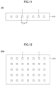
- FIG. 11 is a schematic plan view ( 1 ) exemplifying the planar light source using the light emitting device 1 .
- FIG. 12 is a schematic plan view ( 2 ) exemplifying the planar light source using the light emitting device 1 .
- a planar light source 200 illustrated in FIG. 11 includes the plurality of light emitting devices 1 aligned in a row on a wiring substrate 210 .
- a planar light source 200 A illustrated in FIG. 12 includes the plurality of light emitting devices 1 arranged in a matrix on the wiring substrate 210 .
- pitches (P in FIG. 11 ) of the plurality of light emitting devices 1 are preferably the same, but may be different.
- the pitch of the light emitting devices 1 can be appropriately adjusted depending on the size, brightness, and the like of the light emitting device.
- the pitch of the light emitting devices 1 is, for example, in a range from 5 mm to 100 mm, and is preferably in a range from 8 mm to 50 mm.
- FIG. 13 is a schematic plan view illustrating a specific example of the planar light source using the light emitting device 1 .
- FIG. 14 is a schematic partial cross-sectional view taken along line XIV-XIV in FIG. 13 illustrating a specific example of the planar light source using the light emitting device 1 . Note that, FIG. 13 illustrates members below a partition member 320 illustrated in FIG. 14 .
- a planar light source 300 illustrated in FIGS. 13 and 14 includes the light emitting devices 1 , a wiring substrate 310 , and the partition members 320 .
- the wiring substrate 310 includes an insulating base material 311 and a wire 312 provided on the base material 311 , and may include an insulating resin 313 covering a part of the wire 312 as necessary.
- the insulating resin 313 preferably has light reflectivity.
- the partition member 320 is disposed on the same side as the light emitting device 1 of the wiring substrate 310 .
- the partition member 320 includes a top portion 321 located in a grid shape in plan view, a wall portion 322 surrounding each of the light emitting devices 1 in plan view, and a bottom portion 323 connected to a lower end of the wall portion 322 , and has a plurality of regions each surrounding the light emitting device 1 .
- the wall portion 322 of the partition member 320 extends from the top portion 321 to the wiring substrate 310 side, for example, and a width of a region surrounded by opposing wall portions 322 becomes narrower as becoming closer to the wiring substrate 310 side in the cross-sectional view.
- the light emitting device 1 is disposed in a through hole provided substantially at the center of the bottom portion 323 .
- the partition member 320 is preferably a member having light reflectivity.
- a range (that is, a region and space) surrounded by the wall portions 322 is defined as one partition 300 C, and the partition member 320 includes a plurality of the partitions 300 C.
- one light emitting device 1 is disposed in one partition 300 C.
- the partition member 320 including the bottom portion 323 and the wall portion 322 surrounding each of the light emitting devices 1 is disposed on the wiring substrate 310 , and thus light from the light emitting device 1 can be reflected by the wall portion 322 and the bottom portion 323 , and extraction efficiency of light can be improved. Further, unevenness in brightness in each partition 300 C and, furthermore, unevenness in brightness in group units of the partitions 300 C can be suppressed.
- the partition 300 C has, for example, a rectangle shape in plan view.
- the partition member 320 is, for example, a reflector including the plurality of partitions 300 C that have a rectangle shape in plan view.
- a distance from the center of the light emitting device 1 to four corners of the partition 300 C is longer than a distance to another portion, and thus the four corners of the partition 300 C tend to be dark. When the four corners are dark in each of the partitions 300 C, unevenness in brightness will occur in the planar light source 300 .
- the light-transmissive member 40 has a square shape in plan view in the light emitting device 1 , directivity in the diagonal line direction of the square is improved, and the intensity of light in the diagonal line direction is set higher than the intensity of light in the direction perpendicular to the center of each side of the square and the like.
- darkness at the four corners of the partition 300 C can be suppressed in the planar light source 300 , and unevenness in brightness can be reduced.
- the encapsulant 30 contains a phosphor, unevenness in brightness and color in each of the partitions 300 C can be suppressed and, furthermore, unevenness in brightness and color in the group units of the partitions 300 C can be suppressed.
- the planar light source 300 may include an optical member 330 on or above the top portion 321 of the partition member 320 .
- the optical member 330 can include at least one kind selected from a group consisting of a light diffusion plate 331 , a prism sheet (a first prism sheet 332 and a second prism sheet 333 ), and a polarizing sheet 334 .
- a prism sheet a first prism sheet 332 and a second prism sheet 333
- a polarizing sheet 334 a polarizing sheet 334 .
- the optical member 330 is disposed on or above the top portion 321 of the partition member 320 , and furthermore, a liquid crystal panel is disposed on the optical member 330 , and the planar light source 300 can be used as a light source for direct backlight.
- the order of layering each member in the optical member 330 can be set as desired. Note that the optical member 330 may not be in contact with the top portion 321 of the partition member 320 .
- the light diffusion plate 331 is disposed in contact with the top portion 321 of the partition member 320 above the light emitting device 1 .
- the light diffusion plate 331 preferably has a flat plate-like shape, but may has protrusion(s) and depression(s) on a surface of the light diffusion plate 331 .
- the light diffusion plate 331 is preferably disposed substantially parallel to the wiring substrate 310 .
- the light diffusion plate 331 can be formed of a material having low light absorption for visible light, such as a polycarbonate resin, a polystyrene resin, an acrylic resin, and a polyethylene resin.
- the light diffusion plate 331 may be provided with protrusion(s) and depression(s) on the surface thereof, and a material having a different refractive index may be dispersed in the light diffusion plate 331 .
- the size of the protrusion(s) and the depression(s) can be, for example, in a range from 0.01 mm to 0.1 mm.
- a polycarbonate resin, an acrylic resin, or the like can be used as the material having the different refractive index.
- a thickness of the light diffusion plate 331 and a degree of light diffusion can be set as appropriate, and a commercially available member such as a light diffusion sheet or a diffuser film can be used.
- the thickness of the light diffusion plate 331 can be in a range from 1 mm to 2 mm.
- the first prism sheet 332 and the second prism sheet 333 have a shape in which a plurality of prisms extending in a predetermined direction are arranged on a surface thereof.
- the first prism sheet 332 can include a plurality of prisms extending in the Y direction
- the second prism sheet 333 can include a plurality of prisms extending in the X direction.
- the first prism sheet 332 and the second prism sheet 333 can refract light incident from various directions toward a display panel facing the planar light source 300 . In this way, the light emitted from a light emitting surface of the planar light source 300 can be emitted mainly in a direction perpendicular to an upper surface, and brightness when the planar light source 300 is viewed from the top can be increased.
- the polarizing sheet 334 can selectively transmit light in a polarization direction that matches the polarization direction of a polarizing plate disposed on a backlight side of the display panel such as a liquid crystal display panel, and can reflect polarized light, which is polarized in a direction perpendicular to the polarization direction, toward the first prism sheet 332 and the second prism sheet 333 side. A part of the polarized light returned from the polarizing sheet 334 is reflected again by the first prism sheet 332 , the second prism sheet 333 , and the light diffusion plate 331 .
- the reflected light changes in the polarization direction, and is, for example, converted into polarized light having the polarization direction of the polarizing plate of the liquid crystal display panel, is again incident on the polarizing sheet 334 , and is emitted to the display panel.
- the polarization direction of the light emitted from the planar light source 300 can be aligned, and light in the polarization direction effective for improving the brightness of the display panel can be emitted with high efficiency.
- a commercially available optical member for backlight can be used as the polarizing sheet 334 , the first prism sheet 332 , the second prism sheet 333 , and the like.
- the planar light source 300 can be manufactured by, for example, disposing the partition member 320 and the light emitting device 1 on the wiring substrate 310 and disposing the optical member 330 on or above the partition member 320 as necessary.
- FIG. 15 is a schematic cross-sectional view ( 1 ) exemplifying a light emitting device according to the first modification example of the first embodiment.
- the light source 20 is mounted on the upper surface 10 a of the substrate 10 with the electrode 20 t facing the substrate 10 side.
- the pair of electrodes 20 t of the light source 20 are electrically connected to the pair of leads 11 of the substrate 10 through a conductive joint member.
- the light source 20 is disposed on the substrate 10 with the electrodes 20 t facing the bottom surface of the recessed portion 110 x , and the pair of electrodes 20 t and the pair of leads 11 of the substrate 10 are electrically connected by the conductive joint member.
- the conductive joint member include conductive paste such as silver, gold, and palladium, a eutectic solder material such as gold-tin and tin-silver-copper, a brazing material such as metal having a low melting point, and a bump including silver, gold, or the like.
- the light source 20 may be mounted on the substrate 10 with the electrode 20 t facing an opposite side to the substrate 10 as illustrated in FIG. 2 , or the light source 20 may be mounted on the substrate 10 with the electrode 20 t facing the substrate 10 side as illustrated in FIG. 15 .
- a light source may have a structure in which an optical member such as a light-transmissive member or a light adjustment member is combined with a light emitting element, instead of being a light emitting element alone.
- an optical member such as a light-transmissive member or a light adjustment member is combined with a light emitting element, instead of being a light emitting element alone.
- FIG. 16 is a schematic cross-sectional view ( 2 ) exemplifying a light emitting device according to the first modification example of the first embodiment.
- a light source 20 B includes a light emitting element 21 , a light-transmissive member 22 , and a covering member 23 .
- the light emitting element 21 has an upper surface 21 a , a lower surface 21 b , and at least a lateral surface 21 c .
- the light emitting element 21 is, for example, an LED. Details of the light emitting element are as described in the first embodiment.
- the light emitting element 21 includes a pair of electrodes 21 t formed on the lower surface 21 b .
- One of the pair of electrodes 21 t is a p-side electrode, and the other is an n-side electrode.
- the light source 20 is mounted on the upper surface 10 a of the substrate 10 with the electrodes 21 t of the light emitting element 21 facing the substrate 10 side.
- the pair of electrodes 21 t of the light emitting element 21 are electrically connected to the pair of leads 11 of the substrate 10 through a conductive joint member.
- the pair of electrodes 21 t that is, the p-side electrode and the n-side electrode
- the pair of electrodes 21 t are used as electrodes of the light source 20 B with no modification, but an external connection electrode connected to each of the p-side electrode and the n-side electrode of the light emitting element 21 may be used as an electrode of the light source 20 B.
- the light-transmissive member 22 covers the upper surface 21 a and the lateral surface 21 c of the light emitting element 21 .
- a lower surface of the light-transmissive member 22 is, for example, in the same plane as the lower surface 21 b of the light emitting element 21 .
- the light-transmissive member 22 may include a light diffusion material and a wavelength conversion member. When the wavelength conversion member is used, a type of wavelength conversion member different from that of the phosphor provided in the encapsulant 30 is preferably used.
- the covering member 23 covers the lower surface 21 b of the light emitting element 21 , a lateral surface of the electrode 21 t , and the lower surface of the light-transmissive member 22 , and exposes a lower surface of the electrode 21 t .
- a lower surface of the light source 20 B is formed of a lower surface of the covering member 23 and the lower surface of the electrode 21 t .
- the covering member 23 is preferably a member that reflects light. Note that the covering member 23 may not be provided.
- the light source 20 B is disposed on the substrate 10 with the electrodes 21 t of the light emitting element 21 facing the bottom surface of the recessed portion 110 x , and the pair of electrodes 21 t and the pair of leads 11 of the substrate 10 are electrically connected by the conductive joint member.
- FIG. 17 is a schematic cross-sectional view ( 3 ) exemplifying a light emitting device according to the first modification example of the first embodiment.
- a light source 20 C includes the light emitting element 21 , the light-transmissive member 22 , the covering member 23 , and a light adjustment member 24 .
- the light adjustment member 24 covers the upper surface of the light-transmissive member 22 .
- the light adjustment member 24 preferably covers the entire upper surface of the light-transmissive member 22 .
- the light adjustment member 24 reflects a portion of the light emitted from the light emitting element 21 , and transmits the other portion of the light emitted from the light emitting element 21 .
- the light source 20 C can be mounted on the substrate 10 by a method similar to that used for the light source 20 B, for example.
- FIG. 18 is a schematic cross-sectional view ( 4 ) exemplifying a light emitting device according to the first modification example of the first embodiment.
- a light emitting device 1 D illustrated in FIG. 18 does not include the substrate 10 .
- the pair of electrodes 21 t of the light emitting element 21 are exposed on a lower surface side of the encapsulant 30 , and each of the electrodes 21 t is electrically connected to an external connection electrode 15 .
- the external connection electrode 15 has a larger area than that of the electrode 21 t when viewed from a lower surface side of the light emitting device 1 D.
- the light source 20 B is disposed on the substrate 10 with the electrodes 21 t of the light emitting element 21 facing the bottom surface of the recessed portion 110 x . Then, the substrate 10 is removed before or after the step illustrated in FIG. 10 according to the first embodiment. Subsequently, a pair of the external connection electrodes 15 respectively electrically connected to the electrodes 21 t of the light emitting element 21 are formed on the lower surface side of the encapsulant 30 by a sputtering method, a plating method, or the like. In this case, a support plate formed of metal, resin, or the like may be used as the substrate 10 .
- a second embodiment will be described with reference to FIGS. 19 to 23 .
- FIG. 19 is a schematic plan view exemplifying a light emitting device 2 according to the second embodiment.
- FIG. 20 is a schematic cross-sectional view taken along line II-II in FIG. 19 exemplifying the light emitting device 2 according to the second embodiment.
- the light emitting device 2 includes a substrate 510 , a light source 520 , an encapsulant 530 , and a light-transmissive member 540 .
- the substrate 510 is a member provided as necessary and is not an essential component of the light emitting device 2 .
- the light emitting device 2 according to the second embodiment is different in that the light-transmissive member 40 according to the first embodiment has a rectangle shape in plan view, whereas the light-transmissive member 540 according to the second embodiment has an octagon shape in plan view.
- the second embodiment will be described below, but the description of the first embodiment can be applied to the same points as the first embodiment, and thus a description may be omitted.
- the light-transmissive member 540 has an octagon shape in plan view. All interior angles of the octagon are less than 180 degrees, and the interior angles have different angles. For example, four interior angles indicated by A in FIG. 19 may be the same angle, and four interior angles indicated by B may be the same angle. An angle of the four interior angles indicated by B may be greater than an angle of the four interior angles indicated by A. In this way, light emitted from the light emitting device 2 in the lateral direction can be adjusted such that intensity of the light in a direction in which intensity of the light is high can be reduced, and intensity of the light in a direction in which intensity of the light is low can be increased. Thus, the light emitting device 2 having unevenness in brightness reduced can be obtained.
- the sides of the octagon may have equal lengths.
- the octagon shape may be four-fold symmetrical.
- the octagon shape may include four first vertices 540 v 1 inscribed in a circle C, and other four second vertices 540 v 2 located in a region E surrounded by a chord and an arc determined by the circumferentially adjacent first vertices 540 v 1 .
- the center of the light-transmissive member 540 preferably matches an optical axis of the light source 520 in plan view.
- each vertex of the rectangle shape of the encapsulant 530 is preferably located on an extended line of a diagonal line D 1 or D 2 of the rectangle of the light source 520 .
- the four first vertices 540 v 1 are preferably located on the extended line of the diagonal line D 1 or D 2 of the rectangle of the light source 520 in plan view.
- FIG. 23 is a plan view schematically illustrating a direction of light from a light source using an arrow.
- the light-transmissive member 540 has an octagon shape in plan view, as illustrated in FIG. 23 , most of the light that is emitted from the light source 520 and passes through each side constituting the octagon of the light-transmissive member 540 is refracted in the direction of the diagonal line D 1 or D 2 in plan view.
- directivity in the directions of the diagonal lines D 1 and D 2 can be improved, and the intensity of light in directions of the four first vertices 540 v 1 illustrated in FIG. 22 can be set higher than the intensity of light in directions of the four second vertices 540 v 2 .
- the surface of the light-transmissive member 540 preferably has an inclined surface 540 a having a height on a peripheral end side lower than a height on a center side with reference to a lower surface 20 b of the light source 520 .
- the inclined surface 540 a is provided in, for example, an annular shape outside the encapsulant 530 in plan view.
- an outermost periphery of the inclined surface 540 a is an octagon shape
- an innermost periphery is an octagon shape similar to the outermost periphery.
- the inclined surface 540 a may be formed in a curved shape in the cross-sectional view, may be formed linearly in the cross-sectional view, and is preferably formed linearly in the cross-sectional view.
- the inclined surface 540 a is formed linearly in the cross-sectional view, light emitted in the lateral direction can be increased further than that when the inclined surface 540 a is formed in the curved shape in the cross-sectional view. This is advantageous for wide light distribution.
- a surface of the light-transmissive member 540 includes, outward of the inclined surface 540 a , a flat surface 540 b being a part of a lateral surface of the light emitting device 2 .
- the flat surface 540 b is perpendicular to the lower surface 20 b of the light source 520 .
- the flat surface 540 b is not limited to being perpendicular, and may be inclined with respect to the lower surface 20 b of the light source 520 .
- the flat surface 540 b preferably has a height higher than a height of the light source 520 with reference to the lower surface 20 b of the light source 520 . Light emitted from the light source 520 toward the flat surface 540 b exits from the flat surface 540 b in the lateral direction of the light emitting device 2 .
- the surface of the light-transmissive member 540 preferably has a recessed portion 540 x (i.e., second recessed portion) recessed to the light source 520 side in a region overlapping the encapsulant 530 in plan view.
- the recessed portion 540 x preferably has a deepest portion located at the center of the recessed portion 540 x in plan view.
- An inner surface 540 c of the light-transmissive member 540 that defines the recessed portion 540 x is preferably axisymmetric in a cross section including a central axis that passes through the center of the recessed portion 540 x .
- the recessed portion 540 x defines, for example, a cone shape or a frustum shape.
- the recessed portion 540 x has, for example, a rectangle shape in plan view.
- the recessed portion 540 x defines, for example, a quadrangular pyramid shape or a truncated pyramid shape.
- the center of the recessed portion 540 x preferably matches the optical axis of the light source 520 in plan view.
- the inner surface 540 c may be linearly inclined, or may protrude and be curved toward the outside or the inside of a recess defined by the recessed portion 540 x .
- the inner surface 540 c preferably protrudes and is curved toward the inside of the recess defined by the recessed portion 540 x .
- the surface of the light-transmissive member 540 may include a flat surface 540 d parallel to the lower surface 20 b of the light source 520 between the inclined surface 540 a and the inner surface 540 c that defines the recessed portion 540 x .
- One end side of the flat surface 540 d is continuous with the inclined surface 540 a
- the other end side is continuous with the inner surface 540 c .
- the surface of the light-transmissive member 540 has the recessed portion 540 x recessed to the light source 520 side.
- the light-transmissive member 540 may have a flat surface continuous with the flat surface 540 d .
- the flat surface 540 d when light from the light source 520 hits the flat surface 540 d and the flat surface that is continuous with the flat surface 540 d , a part of the light is reflected by the flat surface and is directed laterally in the light-transmissive member 540 .
- the light emitting device 2 according to the second embodiment has the following characteristics.
- the light emitting device 2 includes a light source, an encapsulant that covers a light emitting surface and a lateral surface of the light source, and a light-transmissive member that covers an upper surface and a lateral surface of the encapsulant.
- the light-transmissive member has an octagon shape in plan view. All interior angles of the octagon are less than 180 degrees, and the interior angles have different angles. The sides of the octagon have equal lengths.
- a surface of the light-transmissive member includes an inclined surface having a height on a peripheral end side lower than a height on a center side with reference to a lower surface of the light source.
- the inclined surface is provided in an annular shape outside the encapsulant in plan view.
- the inclined surface has a linear shape when viewed in a cross-sectional view.
- the surface of the light-transmissive member has, outside the inclined surface, a flat surface perpendicular to the lower surface of the light source.
- the flat surface of the light-transmissive member has a height higher than a height of the light source with reference to the lower surface of the light source.
- the light-transmissive member includes a recessed portion recessed to the light source side in a region overlapping the encapsulant in plan view.
- the recessed portion defines a cone shape or a frustum shape.
- an inner surface of the light-transmissive member that defines the recessed portion protrudes and is curved toward the inside of the recess defined by the recessed portion.
- the recessed portion has a rectangle shape in plan view.
- the surface of the light-transmissive member has a flat surface parallel to the lower surface of the light source between the recessed portion and the inclined surface.
- the recessed portion is larger than the encapsulant in plan view.
- the encapsulant has a rectangle shape in plan view.
- the encapsulant contains a resin and particles of a phosphor.
- the light source has a rectangle shape smaller than the encapsulant in plan view. In plan view, each vertex of the rectangle shape of the encapsulant is located on an extended line of a diagonal line of the rectangle shape of the light source.
- the octagon shape has four first vertices inscribed in a circle, and other four second vertices located in a region surrounded by a chord and an arc determined by the circumferentially adjacent first vertices.
- the first vertex is located on the extended line of the diagonal line of the rectangle shape of the light source in plan view.
- the plurality of light emitting devices 2 according to the second embodiment can also be arranged to be used as a planar light source.
- a liquid crystal display device By using, for a backlight light source, the light emitting device 1 according to the first embodiment or the light emitting device 2 according to the second embodiment as the planar light source, a liquid crystal display device can also be obtained.
- the method for manufacturing the light emitting device 1 according to the first embodiment can also be applied to the method for manufacturing the light emitting device 2 according to the second embodiment.
Landscapes
- Led Device Packages (AREA)
Abstract
Description
Claims (17)
Applications Claiming Priority (4)
| Application Number | Priority Date | Filing Date | Title |
|---|---|---|---|
| JP2020198901A JP7231846B2 (en) | 2020-11-30 | 2020-11-30 | Method for manufacturing light emitting device |
| JP2020-198901 | 2020-11-30 | ||
| JP2021030773A JP7583268B2 (en) | 2021-02-26 | 2021-02-26 | Light-emitting device, light-emitting module, surface light source, liquid crystal display device |
| JP2021-030773 | 2021-02-26 |
Publications (2)
| Publication Number | Publication Date |
|---|---|
| US20220173285A1 US20220173285A1 (en) | 2022-06-02 |
| US12125953B2 true US12125953B2 (en) | 2024-10-22 |
Family
ID=81751777
Family Applications (1)
| Application Number | Title | Priority Date | Filing Date |
|---|---|---|---|
| US17/456,556 Active 2042-12-24 US12125953B2 (en) | 2020-11-30 | 2021-11-24 | Method for manufacturing light emitting device, light emitting device, and light emitting module |
Country Status (1)
| Country | Link |
|---|---|
| US (1) | US12125953B2 (en) |
Citations (24)
| Publication number | Priority date | Publication date | Assignee | Title |
|---|---|---|---|---|
| JP2000252524A (en) | 1999-02-25 | 2000-09-14 | Citizen Electronics Co Ltd | Surface mount type light emitting diode and method of manufacturing the same |
| US20060078246A1 (en) | 2004-10-07 | 2006-04-13 | Towa Corporation | Transparent member, optical device using transparent member and method of manufacturing optical device |
| JP2008147270A (en) | 2006-12-07 | 2008-06-26 | Nichia Chem Ind Ltd | Light emitting device and manufacturing method thereof |
| JP2008270144A (en) | 2007-03-22 | 2008-11-06 | Furukawa Electric Co Ltd:The | light box |
| JP2009272251A (en) | 2008-05-09 | 2009-11-19 | Toshiba Corp | Back light unit |
| WO2009157166A1 (en) | 2008-06-23 | 2009-12-30 | パナソニック株式会社 | Light emitting apparatus, planar light emitting apparatus and display apparatus |
| WO2010095441A1 (en) | 2009-02-19 | 2010-08-26 | シャープ株式会社 | Light emitting device, planar light source, and display device |
| JP2011171765A (en) | 2011-05-24 | 2011-09-01 | Towa Corp | Optical device and method for assembling the same |
| JP2011187979A (en) | 2011-05-24 | 2011-09-22 | Towa Corp | Entire substrate with protecting entire member, and method of manufacturing the same |
| JP2011233645A (en) | 2010-04-26 | 2011-11-17 | Panasonic Corp | A semiconductor device and a method for manufacturing thereof |
| JP2012019149A (en) | 2010-07-09 | 2012-01-26 | Seiko Instruments Inc | Light emitting device |
| WO2012049854A1 (en) | 2010-10-14 | 2012-04-19 | パナソニック株式会社 | Light-emitting device and surface light source device using same |
| JP2012142621A (en) | 2012-04-13 | 2012-07-26 | Apic Yamada Corp | Substrate for led package, manufacturing method of substrate for led package, metallic mold of substrate for led package, led package, and manufacturing method of led package |
| JP2012216764A (en) | 2011-03-25 | 2012-11-08 | Sharp Corp | Light-emitting device, lighting device and display |
| JP2012227203A (en) | 2011-04-15 | 2012-11-15 | Panasonic Corp | Semiconductor device |
| US20130121000A1 (en) * | 2011-11-16 | 2013-05-16 | Song Eun Lee | Light emitting device and lighting apparatus having the same |
| JP2013225713A (en) | 2013-08-08 | 2013-10-31 | Towa Corp | Production method of optical device |
| JP2016081649A (en) | 2014-10-14 | 2016-05-16 | フェニックス電機株式会社 | Led lamp and lens for led lamp |
| US20170069801A1 (en) * | 2015-09-08 | 2017-03-09 | Nichia Corporation | Light emitting device |
| JP2017054929A (en) | 2015-09-09 | 2017-03-16 | 株式会社東芝 | Light emitting device |
| US9786826B2 (en) * | 2015-08-03 | 2017-10-10 | Citizen Electronics Co., Ltd. | LED light-emitting element |
| JP2018088554A (en) | 2018-02-19 | 2018-06-07 | 日亜化学工業株式会社 | Light emitting device |
| US20200111766A1 (en) | 2018-10-04 | 2020-04-09 | Nichia Corporation | Light emitting device |
| US20200135991A1 (en) | 2018-10-31 | 2020-04-30 | Everlight Electronics Co., Ltd. | Lighting device and lighting module |
-
2021
- 2021-11-24 US US17/456,556 patent/US12125953B2/en active Active
Patent Citations (33)
| Publication number | Priority date | Publication date | Assignee | Title |
|---|---|---|---|---|
| JP2000252524A (en) | 1999-02-25 | 2000-09-14 | Citizen Electronics Co Ltd | Surface mount type light emitting diode and method of manufacturing the same |
| US20060078246A1 (en) | 2004-10-07 | 2006-04-13 | Towa Corporation | Transparent member, optical device using transparent member and method of manufacturing optical device |
| JP2006106479A (en) | 2004-10-07 | 2006-04-20 | Towa Corp | Translucent member, optical device, and optical device assembly method |
| JP2008147270A (en) | 2006-12-07 | 2008-06-26 | Nichia Chem Ind Ltd | Light emitting device and manufacturing method thereof |
| US20110063850A1 (en) | 2007-03-22 | 2011-03-17 | Furukawa Electric Co., Ltd | Light box |
| JP2008270144A (en) | 2007-03-22 | 2008-11-06 | Furukawa Electric Co Ltd:The | light box |
| JP2009272251A (en) | 2008-05-09 | 2009-11-19 | Toshiba Corp | Back light unit |
| WO2009157166A1 (en) | 2008-06-23 | 2009-12-30 | パナソニック株式会社 | Light emitting apparatus, planar light emitting apparatus and display apparatus |
| US20100259706A1 (en) | 2008-06-23 | 2010-10-14 | Takashi Kuwaharada | Light-emitting device, surface light-emitting apparatus, display system |
| WO2010095441A1 (en) | 2009-02-19 | 2010-08-26 | シャープ株式会社 | Light emitting device, planar light source, and display device |
| US20110291131A1 (en) | 2009-02-19 | 2011-12-01 | Shin Ito | Light emitting device, planar light source, and display device |
| JP2011233645A (en) | 2010-04-26 | 2011-11-17 | Panasonic Corp | A semiconductor device and a method for manufacturing thereof |
| JP2012019149A (en) | 2010-07-09 | 2012-01-26 | Seiko Instruments Inc | Light emitting device |
| WO2012049854A1 (en) | 2010-10-14 | 2012-04-19 | パナソニック株式会社 | Light-emitting device and surface light source device using same |
| US20130170208A1 (en) * | 2010-10-14 | 2013-07-04 | Panasonic Corporation | Light-emitting device and surface light source device using same |
| JP2012216764A (en) | 2011-03-25 | 2012-11-08 | Sharp Corp | Light-emitting device, lighting device and display |
| JP2012227203A (en) | 2011-04-15 | 2012-11-15 | Panasonic Corp | Semiconductor device |
| JP2011187979A (en) | 2011-05-24 | 2011-09-22 | Towa Corp | Entire substrate with protecting entire member, and method of manufacturing the same |
| JP2011171765A (en) | 2011-05-24 | 2011-09-01 | Towa Corp | Optical device and method for assembling the same |
| US20130121000A1 (en) * | 2011-11-16 | 2013-05-16 | Song Eun Lee | Light emitting device and lighting apparatus having the same |
| JP2013106047A (en) | 2011-11-16 | 2013-05-30 | Lg Innotek Co Ltd | Light emitting element and lighting device including the same |
| JP2012142621A (en) | 2012-04-13 | 2012-07-26 | Apic Yamada Corp | Substrate for led package, manufacturing method of substrate for led package, metallic mold of substrate for led package, led package, and manufacturing method of led package |
| JP2013225713A (en) | 2013-08-08 | 2013-10-31 | Towa Corp | Production method of optical device |
| JP2016081649A (en) | 2014-10-14 | 2016-05-16 | フェニックス電機株式会社 | Led lamp and lens for led lamp |
| US9786826B2 (en) * | 2015-08-03 | 2017-10-10 | Citizen Electronics Co., Ltd. | LED light-emitting element |
| US20170069801A1 (en) * | 2015-09-08 | 2017-03-09 | Nichia Corporation | Light emitting device |
| JP2017054894A (en) | 2015-09-08 | 2017-03-16 | 日亜化学工業株式会社 | Light emitting device |
| JP2017054929A (en) | 2015-09-09 | 2017-03-16 | 株式会社東芝 | Light emitting device |
| JP2018088554A (en) | 2018-02-19 | 2018-06-07 | 日亜化学工業株式会社 | Light emitting device |
| US20200111766A1 (en) | 2018-10-04 | 2020-04-09 | Nichia Corporation | Light emitting device |
| JP2020061543A (en) | 2018-10-04 | 2020-04-16 | 日亜化学工業株式会社 | Light-emitting device |
| US20200135991A1 (en) | 2018-10-31 | 2020-04-30 | Everlight Electronics Co., Ltd. | Lighting device and lighting module |
| JP2020072264A (en) | 2018-10-31 | 2020-05-07 | 億光電子工業股▲ふん▼有限公司Everlight Electronics Co.,Ltd. | Lighting devices and lighting modules |
Also Published As
| Publication number | Publication date |
|---|---|
| US20220173285A1 (en) | 2022-06-02 |
Similar Documents
| Publication | Publication Date | Title |
|---|---|---|
| US8482016B2 (en) | Semiconductor light-emitting device and manufacturing method | |
| US11201269B2 (en) | Backlight including light emitting module and light reflective members | |
| US10763408B2 (en) | Backlight including light emitting module and light reflective members | |
| US11901498B2 (en) | Light-emitting unit and surface-emission light source | |
| US12148870B2 (en) | LED package and integrated light emitting device | |
| US10930624B2 (en) | Light-emitting module | |
| US11342314B2 (en) | Light-emitting module | |
| US12132157B2 (en) | Light emitting module and liquid crystal display device | |
| US20190006568A1 (en) | Light emitting device | |
| US12125953B2 (en) | Method for manufacturing light emitting device, light emitting device, and light emitting module | |
| JP7583268B2 (en) | Light-emitting device, light-emitting module, surface light source, liquid crystal display device | |
| US20240105891A1 (en) | Method of manufacturing light emitting device and light emitting device | |
| JP7656184B2 (en) | Light-emitting device | |
| JP7583304B2 (en) | Light emitting device, surface light source | |
| CN214956934U (en) | Light-emitting device and light-emitting module including the same | |
| US12158659B2 (en) | Reflective member, planar light source, and liquid crystal display device | |
| US20240405171A1 (en) | Light-emitting device, planar light source, and liquid crystal display device | |
| US12206052B2 (en) | Light-emitting device and planar light source that utilizes multiple wavelength conversion layers | |
| US20240258471A1 (en) | Planar light source |
Legal Events
| Date | Code | Title | Description |
|---|---|---|---|
| AS | Assignment |
Owner name: NICHIA CORPORATION, JAPAN Free format text: ASSIGNMENT OF ASSIGNORS INTEREST;ASSIGNORS:SASAOKA, SHIMPEI;HASHIMOTO, TOSHIYUKI;KATSUMATA, TOSHINOBU;AND OTHERS;REEL/FRAME:058209/0940 Effective date: 20211117 |
|
| FEPP | Fee payment procedure |
Free format text: ENTITY STATUS SET TO UNDISCOUNTED (ORIGINAL EVENT CODE: BIG.); ENTITY STATUS OF PATENT OWNER: LARGE ENTITY |
|
| STPP | Information on status: patent application and granting procedure in general |
Free format text: DOCKETED NEW CASE - READY FOR EXAMINATION |
|
| STPP | Information on status: patent application and granting procedure in general |
Free format text: NON FINAL ACTION MAILED |
|
| STPP | Information on status: patent application and granting procedure in general |
Free format text: RESPONSE TO NON-FINAL OFFICE ACTION ENTERED AND FORWARDED TO EXAMINER |
|
| STPP | Information on status: patent application and granting procedure in general |
Free format text: NOTICE OF ALLOWANCE MAILED -- APPLICATION RECEIVED IN OFFICE OF PUBLICATIONS |
|
| ZAAB | Notice of allowance mailed |
Free format text: ORIGINAL CODE: MN/=. |
|
| STPP | Information on status: patent application and granting procedure in general |
Free format text: NOTICE OF ALLOWANCE MAILED -- APPLICATION RECEIVED IN OFFICE OF PUBLICATIONS |
|
| STPP | Information on status: patent application and granting procedure in general |
Free format text: PUBLICATIONS -- ISSUE FEE PAYMENT RECEIVED |
|
| STPP | Information on status: patent application and granting procedure in general |
Free format text: PUBLICATIONS -- ISSUE FEE PAYMENT VERIFIED |
|
| STCF | Information on status: patent grant |
Free format text: PATENTED CASE |