US12097015B2 - Liquid flow induced power generation using nanoscale metal layers - Google Patents
Liquid flow induced power generation using nanoscale metal layers Download PDFInfo
- Publication number
- US12097015B2 US12097015B2 US17/276,684 US201917276684A US12097015B2 US 12097015 B2 US12097015 B2 US 12097015B2 US 201917276684 A US201917276684 A US 201917276684A US 12097015 B2 US12097015 B2 US 12097015B2
- Authority
- US
- United States
- Prior art keywords
- metal
- flow
- metal layer
- current
- nanolayer
- Prior art date
- Legal status (The legal status is an assumption and is not a legal conclusion. Google has not performed a legal analysis and makes no representation as to the accuracy of the status listed.)
- Active, expires
Links
- 229910052751 metal Inorganic materials 0.000 title claims abstract description 158
- 239000002184 metal Substances 0.000 title claims abstract description 157
- 239000007788 liquid Substances 0.000 title claims description 27
- 238000010248 power generation Methods 0.000 title description 6
- 229910044991 metal oxide Inorganic materials 0.000 claims abstract description 70
- 150000004706 metal oxides Chemical class 0.000 claims abstract description 70
- 238000000034 method Methods 0.000 claims abstract description 36
- 238000003306 harvesting Methods 0.000 claims abstract description 15
- XEEYBQQBJWHFJM-UHFFFAOYSA-N Iron Chemical compound [Fe] XEEYBQQBJWHFJM-UHFFFAOYSA-N 0.000 claims description 110
- 239000000243 solution Substances 0.000 claims description 81
- XLYOFNOQVPJJNP-UHFFFAOYSA-N water Substances O XLYOFNOQVPJJNP-UHFFFAOYSA-N 0.000 claims description 52
- 229910052742 iron Inorganic materials 0.000 claims description 40
- PXHVJJICTQNCMI-UHFFFAOYSA-N Nickel Chemical compound [Ni] PXHVJJICTQNCMI-UHFFFAOYSA-N 0.000 claims description 38
- 150000002500 ions Chemical class 0.000 claims description 30
- 230000033001 locomotion Effects 0.000 claims description 19
- 229910052759 nickel Inorganic materials 0.000 claims description 15
- 238000004146 energy storage Methods 0.000 claims description 8
- 230000003647 oxidation Effects 0.000 claims description 8
- 238000007254 oxidation reaction Methods 0.000 claims description 8
- 239000012266 salt solution Substances 0.000 claims description 8
- LEONUFNNVUYDNQ-UHFFFAOYSA-N vanadium atom Chemical compound [V] LEONUFNNVUYDNQ-UHFFFAOYSA-N 0.000 claims description 8
- 239000002800 charge carrier Substances 0.000 claims description 7
- 239000000203 mixture Substances 0.000 claims description 7
- 229910052720 vanadium Inorganic materials 0.000 claims description 7
- 239000008280 blood Substances 0.000 claims description 5
- 210000004369 blood Anatomy 0.000 claims description 5
- 239000002019 doping agent Substances 0.000 claims description 5
- 229910052802 copper Inorganic materials 0.000 claims description 4
- 239000010949 copper Substances 0.000 claims description 4
- RYGMFSIKBFXOCR-UHFFFAOYSA-N Copper Chemical compound [Cu] RYGMFSIKBFXOCR-UHFFFAOYSA-N 0.000 claims description 3
- 239000000956 alloy Substances 0.000 claims description 2
- 229910045601 alloy Inorganic materials 0.000 claims description 2
- 210000001367 artery Anatomy 0.000 claims description 2
- 210000003462 vein Anatomy 0.000 claims description 2
- 239000013535 sea water Substances 0.000 abstract description 2
- 239000002052 molecular layer Substances 0.000 description 82
- 235000002639 sodium chloride Nutrition 0.000 description 46
- FAPWRFPIFSIZLT-UHFFFAOYSA-M Sodium chloride Chemical compound [Na+].[Cl-] FAPWRFPIFSIZLT-UHFFFAOYSA-M 0.000 description 39
- 229910015189 FeOx Inorganic materials 0.000 description 27
- 210000004027 cell Anatomy 0.000 description 26
- 150000003839 salts Chemical class 0.000 description 23
- 238000004088 simulation Methods 0.000 description 23
- 239000011780 sodium chloride Substances 0.000 description 21
- UQSXHKLRYXJYBZ-UHFFFAOYSA-N Iron oxide Chemical compound [Fe]=O UQSXHKLRYXJYBZ-UHFFFAOYSA-N 0.000 description 20
- 229910052782 aluminium Inorganic materials 0.000 description 16
- 239000011651 chromium Substances 0.000 description 15
- -1 Na+ cation Chemical class 0.000 description 14
- 238000004833 X-ray photoelectron spectroscopy Methods 0.000 description 13
- 239000003570 air Substances 0.000 description 12
- XAGFODPZIPBFFR-UHFFFAOYSA-N aluminium Chemical compound [Al] XAGFODPZIPBFFR-UHFFFAOYSA-N 0.000 description 12
- 238000009826 distribution Methods 0.000 description 12
- 239000002120 nanofilm Substances 0.000 description 12
- 230000003993 interaction Effects 0.000 description 11
- 238000002474 experimental method Methods 0.000 description 10
- 238000005259 measurement Methods 0.000 description 10
- 239000007864 aqueous solution Substances 0.000 description 9
- 239000004020 conductor Substances 0.000 description 9
- 230000000694 effects Effects 0.000 description 9
- 239000011521 glass Substances 0.000 description 9
- 150000002739 metals Chemical group 0.000 description 9
- 229910017107 AlOx Inorganic materials 0.000 description 8
- 229910052804 chromium Inorganic materials 0.000 description 8
- 229910000480 nickel oxide Inorganic materials 0.000 description 8
- GNRSAWUEBMWBQH-UHFFFAOYSA-N oxonickel Chemical compound [Ni]=O GNRSAWUEBMWBQH-UHFFFAOYSA-N 0.000 description 8
- 238000005240 physical vapour deposition Methods 0.000 description 8
- 239000000523 sample Substances 0.000 description 8
- 229910019923 CrOx Inorganic materials 0.000 description 7
- 229910005855 NiOx Inorganic materials 0.000 description 7
- 210000001787 dendrite Anatomy 0.000 description 7
- 230000006870 function Effects 0.000 description 7
- 238000000329 molecular dynamics simulation Methods 0.000 description 7
- VYZAMTAEIAYCRO-UHFFFAOYSA-N Chromium Chemical compound [Cr] VYZAMTAEIAYCRO-UHFFFAOYSA-N 0.000 description 6
- 238000013459 approach Methods 0.000 description 6
- 230000027756 respiratory electron transport chain Effects 0.000 description 6
- 239000000758 substrate Substances 0.000 description 6
- 229910009523 YCl3 Inorganic materials 0.000 description 5
- 239000012080 ambient air Substances 0.000 description 5
- 230000015572 biosynthetic process Effects 0.000 description 5
- 230000008859 change Effects 0.000 description 5
- 238000005421 electrostatic potential Methods 0.000 description 5
- 239000004065 semiconductor Substances 0.000 description 5
- 238000004611 spectroscopical analysis Methods 0.000 description 5
- PCMOZDDGXKIOLL-UHFFFAOYSA-K yttrium chloride Chemical compound [Cl-].[Cl-].[Cl-].[Y+3] PCMOZDDGXKIOLL-UHFFFAOYSA-K 0.000 description 5
- 238000006243 chemical reaction Methods 0.000 description 4
- 230000000875 corresponding effect Effects 0.000 description 4
- 239000007787 solid Substances 0.000 description 4
- 229910052725 zinc Inorganic materials 0.000 description 4
- 239000011701 zinc Substances 0.000 description 4
- OKTJSMMVPCPJKN-UHFFFAOYSA-N Carbon Chemical compound [C] OKTJSMMVPCPJKN-UHFFFAOYSA-N 0.000 description 3
- 239000004743 Polypropylene Substances 0.000 description 3
- FKNQFGJONOIPTF-UHFFFAOYSA-N Sodium cation Chemical compound [Na+] FKNQFGJONOIPTF-UHFFFAOYSA-N 0.000 description 3
- HCHKCACWOHOZIP-UHFFFAOYSA-N Zinc Chemical compound [Zn] HCHKCACWOHOZIP-UHFFFAOYSA-N 0.000 description 3
- 230000009471 action Effects 0.000 description 3
- 239000012267 brine Substances 0.000 description 3
- 238000013461 design Methods 0.000 description 3
- SZVJSHCCFOBDDC-UHFFFAOYSA-N ferrosoferric oxide Chemical compound O=[Fe]O[Fe]O[Fe]=O SZVJSHCCFOBDDC-UHFFFAOYSA-N 0.000 description 3
- 230000005484 gravity Effects 0.000 description 3
- 230000010287 polarization Effects 0.000 description 3
- 229920001155 polypropylene Polymers 0.000 description 3
- 238000012216 screening Methods 0.000 description 3
- HPALAKNZSZLMCH-UHFFFAOYSA-M sodium;chloride;hydrate Chemical compound O.[Na+].[Cl-] HPALAKNZSZLMCH-UHFFFAOYSA-M 0.000 description 3
- 238000003860 storage Methods 0.000 description 3
- 230000005641 tunneling Effects 0.000 description 3
- VTLYFUHAOXGGBS-UHFFFAOYSA-N Fe3+ Chemical compound [Fe+3] VTLYFUHAOXGGBS-UHFFFAOYSA-N 0.000 description 2
- 238000001069 Raman spectroscopy Methods 0.000 description 2
- 239000004809 Teflon Substances 0.000 description 2
- 229920006362 Teflon® Polymers 0.000 description 2
- ATJFFYVFTNAWJD-UHFFFAOYSA-N Tin Chemical compound [Sn] ATJFFYVFTNAWJD-UHFFFAOYSA-N 0.000 description 2
- 238000002441 X-ray diffraction Methods 0.000 description 2
- 239000008346 aqueous phase Substances 0.000 description 2
- QVGXLLKOCUKJST-UHFFFAOYSA-N atomic oxygen Chemical compound [O] QVGXLLKOCUKJST-UHFFFAOYSA-N 0.000 description 2
- 230000008901 benefit Effects 0.000 description 2
- 230000032770 biofilm formation Effects 0.000 description 2
- 230000017531 blood circulation Effects 0.000 description 2
- 238000004364 calculation method Methods 0.000 description 2
- 239000003990 capacitor Substances 0.000 description 2
- 150000001768 cations Chemical class 0.000 description 2
- 238000005229 chemical vapour deposition Methods 0.000 description 2
- JOPOVCBBYLSVDA-UHFFFAOYSA-N chromium(6+) Chemical compound [Cr+6] JOPOVCBBYLSVDA-UHFFFAOYSA-N 0.000 description 2
- 239000011248 coating agent Substances 0.000 description 2
- 238000000576 coating method Methods 0.000 description 2
- 239000008367 deionised water Substances 0.000 description 2
- 229910021641 deionized water Inorganic materials 0.000 description 2
- 238000000151 deposition Methods 0.000 description 2
- 238000010612 desalination reaction Methods 0.000 description 2
- 239000011888 foil Substances 0.000 description 2
- 229910021389 graphene Inorganic materials 0.000 description 2
- 229910052595 hematite Inorganic materials 0.000 description 2
- 239000011019 hematite Substances 0.000 description 2
- 230000006872 improvement Effects 0.000 description 2
- 238000001727 in vivo Methods 0.000 description 2
- 238000011835 investigation Methods 0.000 description 2
- LIKBJVNGSGBSGK-UHFFFAOYSA-N iron(3+);oxygen(2-) Chemical compound [O-2].[O-2].[O-2].[Fe+3].[Fe+3] LIKBJVNGSGBSGK-UHFFFAOYSA-N 0.000 description 2
- 230000002045 lasting effect Effects 0.000 description 2
- 230000000670 limiting effect Effects 0.000 description 2
- 238000004519 manufacturing process Methods 0.000 description 2
- 239000000463 material Substances 0.000 description 2
- 230000007246 mechanism Effects 0.000 description 2
- 238000012986 modification Methods 0.000 description 2
- 230000004048 modification Effects 0.000 description 2
- 238000012544 monitoring process Methods 0.000 description 2
- 230000003287 optical effect Effects 0.000 description 2
- 229910052760 oxygen Inorganic materials 0.000 description 2
- 239000001301 oxygen Substances 0.000 description 2
- 229920001296 polysiloxane Polymers 0.000 description 2
- 230000008569 process Effects 0.000 description 2
- 238000005086 pumping Methods 0.000 description 2
- 230000005855 radiation Effects 0.000 description 2
- 230000009467 reduction Effects 0.000 description 2
- 230000002441 reversible effect Effects 0.000 description 2
- 238000005096 rolling process Methods 0.000 description 2
- 229910052709 silver Inorganic materials 0.000 description 2
- 235000011888 snacks Nutrition 0.000 description 2
- 239000007858 starting material Substances 0.000 description 2
- 230000002123 temporal effect Effects 0.000 description 2
- 229910052718 tin Inorganic materials 0.000 description 2
- 238000003325 tomography Methods 0.000 description 2
- 229910001935 vanadium oxide Inorganic materials 0.000 description 2
- 239000002699 waste material Substances 0.000 description 2
- 238000009736 wetting Methods 0.000 description 2
- 238000010146 3D printing Methods 0.000 description 1
- 241000270728 Alligator Species 0.000 description 1
- OYPRJOBELJOOCE-UHFFFAOYSA-N Calcium Chemical compound [Ca] OYPRJOBELJOOCE-UHFFFAOYSA-N 0.000 description 1
- QPLDLSVMHZLSFG-UHFFFAOYSA-N Copper oxide Chemical compound [Cu]=O QPLDLSVMHZLSFG-UHFFFAOYSA-N 0.000 description 1
- 239000005751 Copper oxide Substances 0.000 description 1
- CWYNVVGOOAEACU-UHFFFAOYSA-N Fe2+ Chemical compound [Fe+2] CWYNVVGOOAEACU-UHFFFAOYSA-N 0.000 description 1
- DGAQECJNVWCQMB-PUAWFVPOSA-M Ilexoside XXIX Chemical compound C[C@@H]1CC[C@@]2(CC[C@@]3(C(=CC[C@H]4[C@]3(CC[C@@H]5[C@@]4(CC[C@@H](C5(C)C)OS(=O)(=O)[O-])C)C)[C@@H]2[C@]1(C)O)C)C(=O)O[C@H]6[C@@H]([C@H]([C@@H]([C@H](O6)CO)O)O)O.[Na+] DGAQECJNVWCQMB-PUAWFVPOSA-M 0.000 description 1
- FYYHWMGAXLPEAU-UHFFFAOYSA-N Magnesium Chemical compound [Mg] FYYHWMGAXLPEAU-UHFFFAOYSA-N 0.000 description 1
- VVQNEPGJFQJSBK-UHFFFAOYSA-N Methyl methacrylate Chemical compound COC(=O)C(C)=C VVQNEPGJFQJSBK-UHFFFAOYSA-N 0.000 description 1
- CBENFWSGALASAD-UHFFFAOYSA-N Ozone Chemical compound [O-][O+]=O CBENFWSGALASAD-UHFFFAOYSA-N 0.000 description 1
- 229920005372 Plexiglas® Polymers 0.000 description 1
- 239000004698 Polyethylene Substances 0.000 description 1
- BQCADISMDOOEFD-UHFFFAOYSA-N Silver Chemical compound [Ag] BQCADISMDOOEFD-UHFFFAOYSA-N 0.000 description 1
- 229910003087 TiOx Inorganic materials 0.000 description 1
- 101150110932 US19 gene Proteins 0.000 description 1
- XHCLAFWTIXFWPH-UHFFFAOYSA-N [O-2].[O-2].[O-2].[O-2].[O-2].[V+5].[V+5] Chemical compound [O-2].[O-2].[O-2].[O-2].[O-2].[V+5].[V+5] XHCLAFWTIXFWPH-UHFFFAOYSA-N 0.000 description 1
- 238000002835 absorbance Methods 0.000 description 1
- 239000002253 acid Substances 0.000 description 1
- AZDRQVAHHNSJOQ-UHFFFAOYSA-N alumane Chemical compound [AlH3] AZDRQVAHHNSJOQ-UHFFFAOYSA-N 0.000 description 1
- 238000004458 analytical method Methods 0.000 description 1
- 150000001450 anions Chemical class 0.000 description 1
- 238000000429 assembly Methods 0.000 description 1
- 230000000712 assembly Effects 0.000 description 1
- 230000003190 augmentative effect Effects 0.000 description 1
- 230000004888 barrier function Effects 0.000 description 1
- 230000009286 beneficial effect Effects 0.000 description 1
- 210000001124 body fluid Anatomy 0.000 description 1
- 238000009835 boiling Methods 0.000 description 1
- 229910052791 calcium Inorganic materials 0.000 description 1
- 239000011575 calcium Substances 0.000 description 1
- 238000004422 calculation algorithm Methods 0.000 description 1
- 239000002041 carbon nanotube Substances 0.000 description 1
- 229910021393 carbon nanotube Inorganic materials 0.000 description 1
- BFGKITSFLPAWGI-UHFFFAOYSA-N chromium(3+) Chemical compound [Cr+3] BFGKITSFLPAWGI-UHFFFAOYSA-N 0.000 description 1
- 238000000205 computational method Methods 0.000 description 1
- 239000000356 contaminant Substances 0.000 description 1
- 230000001276 controlling effect Effects 0.000 description 1
- 229910000431 copper oxide Inorganic materials 0.000 description 1
- 230000002596 correlated effect Effects 0.000 description 1
- 230000008878 coupling Effects 0.000 description 1
- 238000010168 coupling process Methods 0.000 description 1
- 238000005859 coupling reaction Methods 0.000 description 1
- 239000013078 crystal Substances 0.000 description 1
- 125000004122 cyclic group Chemical group 0.000 description 1
- 238000013016 damping Methods 0.000 description 1
- 230000001419 dependent effect Effects 0.000 description 1
- 230000008021 deposition Effects 0.000 description 1
- 238000003795 desorption Methods 0.000 description 1
- 238000006073 displacement reaction Methods 0.000 description 1
- 230000009977 dual effect Effects 0.000 description 1
- 239000003792 electrolyte Substances 0.000 description 1
- 238000005328 electron beam physical vapour deposition Methods 0.000 description 1
- 238000010894 electron beam technology Methods 0.000 description 1
- 238000000313 electron-beam-induced deposition Methods 0.000 description 1
- 230000009881 electrostatic interaction Effects 0.000 description 1
- 238000000572 ellipsometry Methods 0.000 description 1
- 238000011067 equilibration Methods 0.000 description 1
- 238000005530 etching Methods 0.000 description 1
- 238000000605 extraction Methods 0.000 description 1
- 239000003673 groundwater Substances 0.000 description 1
- JEGUKCSWCFPDGT-UHFFFAOYSA-N h2o hydrate Chemical compound O.O JEGUKCSWCFPDGT-UHFFFAOYSA-N 0.000 description 1
- 230000036541 health Effects 0.000 description 1
- 125000002887 hydroxy group Chemical group [H]O* 0.000 description 1
- 238000000338 in vitro Methods 0.000 description 1
- 239000012212 insulator Substances 0.000 description 1
- 230000007774 longterm Effects 0.000 description 1
- 229910052749 magnesium Inorganic materials 0.000 description 1
- 239000011777 magnesium Substances 0.000 description 1
- 239000004579 marble Substances 0.000 description 1
- 229910001092 metal group alloy Inorganic materials 0.000 description 1
- 239000013580 millipore water Substances 0.000 description 1
- 238000002156 mixing Methods 0.000 description 1
- 239000002086 nanomaterial Substances 0.000 description 1
- 230000007935 neutral effect Effects 0.000 description 1
- 229920000620 organic polymer Polymers 0.000 description 1
- 230000003534 oscillatory effect Effects 0.000 description 1
- 230000003204 osmotic effect Effects 0.000 description 1
- 230000036961 partial effect Effects 0.000 description 1
- 239000002245 particle Substances 0.000 description 1
- 238000009304 pastoral farming Methods 0.000 description 1
- 230000002572 peristaltic effect Effects 0.000 description 1
- 239000004033 plastic Substances 0.000 description 1
- 229920003023 plastic Polymers 0.000 description 1
- 229920000573 polyethylene Polymers 0.000 description 1
- 229920000642 polymer Polymers 0.000 description 1
- 238000005381 potential energy Methods 0.000 description 1
- 230000002035 prolonged effect Effects 0.000 description 1
- 230000005588 protonation Effects 0.000 description 1
- 230000002829 reductive effect Effects 0.000 description 1
- 230000004044 response Effects 0.000 description 1
- 239000004332 silver Substances 0.000 description 1
- 239000010944 silver (metal) Substances 0.000 description 1
- 239000011734 sodium Substances 0.000 description 1
- 229910052708 sodium Inorganic materials 0.000 description 1
- 239000002904 solvent Substances 0.000 description 1
- 238000001179 sorption measurement Methods 0.000 description 1
- 241000894007 species Species 0.000 description 1
- 230000003068 static effect Effects 0.000 description 1
- CCEKAJIANROZEO-UHFFFAOYSA-N sulfluramid Chemical group CCNS(=O)(=O)C(F)(F)C(F)(F)C(F)(F)C(F)(F)C(F)(F)C(F)(F)C(F)(F)C(F)(F)F CCEKAJIANROZEO-UHFFFAOYSA-N 0.000 description 1
- 239000011135 tin Substances 0.000 description 1
- XOLBLPGZBRYERU-UHFFFAOYSA-N tin dioxide Chemical compound O=[Sn]=O XOLBLPGZBRYERU-UHFFFAOYSA-N 0.000 description 1
- 229910001887 tin oxide Inorganic materials 0.000 description 1
- HLLICFJUWSZHRJ-UHFFFAOYSA-N tioxidazole Chemical compound CCCOC1=CC=C2N=C(NC(=O)OC)SC2=C1 HLLICFJUWSZHRJ-UHFFFAOYSA-N 0.000 description 1
- 230000026683 transduction Effects 0.000 description 1
- 238000010361 transduction Methods 0.000 description 1
- 230000001052 transient effect Effects 0.000 description 1
- 230000007704 transition Effects 0.000 description 1
- 238000007740 vapor deposition Methods 0.000 description 1
- 238000001429 visible spectrum Methods 0.000 description 1
- 239000002351 wastewater Substances 0.000 description 1
- 238000004065 wastewater treatment Methods 0.000 description 1
Images


Classifications
-
- H—ELECTRICITY
- H02—GENERATION; CONVERSION OR DISTRIBUTION OF ELECTRIC POWER
- H02N—ELECTRIC MACHINES NOT OTHERWISE PROVIDED FOR
- H02N1/00—Electrostatic generators or motors using a solid moving electrostatic charge carrier
- H02N1/06—Influence generators
- H02N1/08—Influence generators with conductive charge carrier, i.e. capacitor machines
-
- H—ELECTRICITY
- H02—GENERATION; CONVERSION OR DISTRIBUTION OF ELECTRIC POWER
- H02N—ELECTRIC MACHINES NOT OTHERWISE PROVIDED FOR
- H02N11/00—Generators or motors not provided for elsewhere; Alleged perpetua mobilia obtained by electric or magnetic means
- H02N11/002—Generators
-
- A—HUMAN NECESSITIES
- A61—MEDICAL OR VETERINARY SCIENCE; HYGIENE
- A61B—DIAGNOSIS; SURGERY; IDENTIFICATION
- A61B5/00—Measuring for diagnostic purposes; Identification of persons
- A61B5/02—Detecting, measuring or recording for evaluating the cardiovascular system, e.g. pulse, heart rate, blood pressure or blood flow
- A61B5/026—Measuring blood flow
-
- Y—GENERAL TAGGING OF NEW TECHNOLOGICAL DEVELOPMENTS; GENERAL TAGGING OF CROSS-SECTIONAL TECHNOLOGIES SPANNING OVER SEVERAL SECTIONS OF THE IPC; TECHNICAL SUBJECTS COVERED BY FORMER USPC CROSS-REFERENCE ART COLLECTIONS [XRACs] AND DIGESTS
- Y02—TECHNOLOGIES OR APPLICATIONS FOR MITIGATION OR ADAPTATION AGAINST CLIMATE CHANGE
- Y02B—CLIMATE CHANGE MITIGATION TECHNOLOGIES RELATED TO BUILDINGS, e.g. HOUSING, HOUSE APPLIANCES OR RELATED END-USER APPLICATIONS
- Y02B10/00—Integration of renewable energy sources in buildings
- Y02B10/10—Photovoltaic [PV]
-
- Y—GENERAL TAGGING OF NEW TECHNOLOGICAL DEVELOPMENTS; GENERAL TAGGING OF CROSS-SECTIONAL TECHNOLOGIES SPANNING OVER SEVERAL SECTIONS OF THE IPC; TECHNICAL SUBJECTS COVERED BY FORMER USPC CROSS-REFERENCE ART COLLECTIONS [XRACs] AND DIGESTS
- Y02—TECHNOLOGIES OR APPLICATIONS FOR MITIGATION OR ADAPTATION AGAINST CLIMATE CHANGE
- Y02E—REDUCTION OF GREENHOUSE GAS [GHG] EMISSIONS, RELATED TO ENERGY GENERATION, TRANSMISSION OR DISTRIBUTION
- Y02E10/00—Energy generation through renewable energy sources
- Y02E10/50—Photovoltaic [PV] energy
Definitions
- Energy harvesting devices and methods of using the devices to convert the mechanical energy of a flowing ionic solution into electric energy are provided. Also provided are flow sensors and methods for using the flow sensors to monitor the flow of an ionic solution, as well as frictionless pumps and methods for using the pumps to move an ionic solution across a surface.
- the devices utilize the flowing ionic solution to move an electrical double layer across a metal layer, thereby generating a current in the metal layer.
- One embodiment of a method of harvesting energy uses a liquid flow-based device that includes: a metal layer comprising a metal; an amphoteric metal oxide film adjacent to the metal layer at an interface, the amphoteric metal oxide film having a surface disposed opposite the interface, wherein the metal layer has a thickness that facilitates charge carrier motion parallel to the interface; and at least one of: an electronic device that consumes electrical power connected laterally across the metal layer and configured to be powered by a current running parallel to the interface; and an energy storage device connected laterally across the metal layer and configured to be charged by a current running parallel to the interface.
- the method of harvesting energy using said device includes the steps of: exposing the surface of the amphoteric metal oxide film to a flow of an ionic solution having a temporally varying flow rate or a temporally varying flow direction, wherein the temporally varying flow rate or the temporally varying flow direction generates a current in the metal layer; and powering the electronic device or charging the energy storage device with the generated current.
- the method of monitoring the flow of the ionic solution includes the steps of: exposing the surface of the amphoteric metal oxide film to a flow of an ionic solution to generate a current in the metal layer, the flow of the ionic solution having a temporally varying ionic conductivity, wherein the temporally varying ionic conductivity is provided by a temporally varying flow rate, a temporally varying flow direction, or both; and measuring changes in the voltage across the metal layer or the current through, the metal layer as the ionic solution passes over the surface of the amphoteric metal oxide film.
- One embodiment of a method of pumping an ionic solution uses a liquid flow-based device that includes: a metal layer comprising a metal; an amphoteric metal oxide film adjacent to the metal layer at an interface, the amphoteric metal oxide film having a surface disposed opposite the interface, wherein the metal layer has a thickness that facilitates charge carrier motion parallel to the interface; and a voltage source configured to apply a voltage across the metal layer.
- the method of pumping the ionic solution includes the steps of: disposing an ionic solution on the surface of the amphoteric metal oxide film; and applying a temporally varying voltage across the metal layer, whereby the temporally varying voltage induces the ionic solution to move along the surface of the amphoteric metal oxide film.
- liquid flow-based devices that can be used to carry out the above-described, and other, methods include: a metal layer comprising vanadium, copper, or tin; an amphoteric metal oxide film comprising vanadium oxide, copper oxide, or tin oxide adjacent to the metal layer at an interface, the amphoteric metal oxide film having a surface disposed opposite the interface, wherein the metal layer has a thickness that facilitates charge carrier motion parallel to the interface; and at least one of: an electronic device that consumes electrical power connected laterally across the metal layer and configured to be powered by a current running parallel to the interface; an energy storage device connected laterally across the metal layer and configured to be charged by a current running parallel to the interface; a voltage measuring device configured to measure a voltage across the metal layer; and a current measuring device connected laterally across the metal layer and configured to measure a current running parallel to the interface.
- FIGS. 1 A- 1 C depicts one embodiment of an energy harvesting device.
- FIG. 1 B is a cartoon representation of the use of stacked nanofilms inside a pipe for electrical power extraction from temporally varying ionic solution flows, such as oceanic tides, or flows of alternating salinity in estuaries and fjords.
- FIG. 1 C depicts one embodiment of an energy harvesting device having multiple metal layers and multiple metal oxide overlayers.
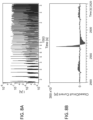
- FIGS. 2 A- 2 C Current and Voltage Measurements.
- FIG. 2 A depicts current induced in a 10 nm Fe:FeOx nanolayer (3 ⁇ 1 in 2 ) when flowing deionized (DI) water at pH 5.8 for 20 sec (black segment), followed by 20 sec flow of 1 M NaCl held at pH 7 (grey segment), and six subsequent replicates, all at a constant flow rate of 20 mL min′.
- FIG. 2 B depicts the same as in FIG. 2 A but measured using a 3 ⁇ 9 in 2 Fe:FeOx nanolayer of 10 nm thickness at a flow rate of 100 mL min ⁇ 1 and 2 min between switching salt concentration.
- FIG. 2 C depicts the same as in FIG. 2 B but measured at a flow rate of 35 mL min ⁇ 1 and constant 0.6 M salt concentration while reversing the flow direction every 2 min, marked by the vertical grey lines.
- FIG. 3 depicts closed circuit current for a 10 nm thin iron nanolayer under flow of 600 mM NaCl at pH 8.0 lasting 2 seconds alternating with air flow lasting 2 seconds at a flow rate of 28 mL min ⁇ 1 .
- FIGS. 4 A- 4 B depict voltage induced in a 50 nm (black trace) and 10 nm (gray trace) thin iron nanofilm (data offset for clarity); 15 ⁇ L drops at a drop rate of 0.5 mL min ⁇ 1 .
- FIG. 4 B depicts voltage induced in a 2 mm thick iron plate, commercial aluminum foil (data offset for clarity), and aluminum film inside a snack bag (data offset for clarity); 15 ⁇ L drops at a drop rate of 0.5 mL min ⁇ 1 .
- OCV open-circuit voltage
- FIG. 7 depicts OCV for a 10 nm thick iron nanofilm using drops alternating between 0.2 mM NaCl at pH 5.8 and 600 mM NaCl at pH 8.0 with a drop rate of 0.5 mL min ⁇ 1 .
- FIGS. 8 A- 8 B depict induced current in a 10 nm iron nanofilm using aqueous solutions of alternating salinity (0.1M and DI water, 25 mL min ⁇ 1 , 20 sec flow per salinity) over ⁇ 1 hour.
- FIG. 8 B depicts induced current before, during, and after low-to-high salinity transition in a flow cell.
- FIGS. 9 A- 9 F Mechanistic Investigations.
- FIG. 9 B depicts the same as FIG. 9 A but for a 10 nm Fe:FeOx nanolayer as a function of aqueous flow velocity and for a 10 nm thin nanolayer of pure FeOx (no metal present) and a 10 nm thin nanolayer of pure TiOx.
- FIG. 9 C depicts current density recorded for Fe:FeOx nanolayers varying in total thickness obtained with a flow velocity of 0.74 cm s ⁇ 1 while alternating DI water and 0.6 M NaCl solution segments every 20 sec.
- FIG. 9 B depicts the same as FIG. 9 A but for a 10 nm Fe:FeOx nanolayer as a function of aqueous flow velocity and for a 10 nm thin nanolayer of pure FeOx (no metal present) and a 10 nm thin nanolayer of pure TiOx.
- FIG. 9 C depicts current density recorded for Fe:FeOx nanolayers varying in total thickness obtained with a flow velocity of 0.74 cm
- FIG. 9 D depicts current density obtained for a 30 nm Fe:FeOx nanolayer without and with a 5 nm Cr:CrOx nanolayer on top of it obtained with a flow velocity of 1.15 cm s ⁇ 1 , and for a 30 nm nanolayer of pure FeOx (no metal present) obtained with a flow velocity of 1 cm s ⁇ 1 , all while alternating DI water and 0.6 M NaCl solution segments every 20 sec.
- FIG. 10 depicts a plot of FIG. 9 B including references provided for the comparison to previously reported results (light grey filled circles).
- FIG. 11 depicts OCV measured for a 20 nm thin aluminum nanofilm using 600 mM salt (pH 5.8) and a drop rate of 0.5 mL/min.
- FIGS. 12 A- 12 E depict X-ray photoelectron spectroscopy (XPS) depth profile graphs of ⁇ 10 nm
- FIG. 12 A Al:AlOx
- FIG. 12 B Cr:CrOx
- FIG. 12 C V:VOx
- FIG. 12 D Fe:FeOx
- FIG. 12 E Ni:NiOx films deposited on microscope slides. Big and small black dashed lines represent peaks for zero-valent and trivalent/divalent forms of the elements identified, respectively.
- the dashed vertical line in FIG. 12 B shows the absence of hexavalent chromium [Cr(VI)] peaks in the CrOx nano-overlayer.
- FIG. 12 C show the presence of V(IV) and V(V) in the VOx nano-overlayers, while the dashed lines show V(0).
- Vertical solid lines in FIG. 12 D and FIG. 12 E show the presence of M(II) and M(III) in the FeOx and NiOx nano-overlayers.
- FIG. 13 is a cartoon representation of electrical energy conversion in metal nanolayers terminated by their thermal oxides.
- FIGS. 14 A- 14 G Model of Charge Mobility in a Nanoconfined, Insulator-Terminated Metal Conductor.
- FIG. 14 A depicts atom probe tomography reconstruction of the heterostructured Fe:FeOx nanolayer (center). Iron oxide and iron metal shown separately on top and bottom, respectively.
- FIG. 14 B depicts an all-atom representation of the heterostructured nanolayer, including the metal conductor (gray) and a nonpolarizable oxide overlayer and with columnar subsurface heterostructure (darker outlined circles); a single probe Na+ cation is shown at a distance of 1.6 angstroms from the nanolayer.
- FIG. 14 A depicts atom probe tomography reconstruction of the heterostructured Fe:FeOx nanolayer (center). Iron oxide and iron metal shown separately on top and bottom, respectively.
- FIG. 14 B depicts an all-atom representation of the heterostructured nanolayer, including the metal conductor (gray) and a nonpolarizable oxide overlayer and with columnar subsurface heterostructure (darker
- FIG. 14 C depicts induced charge distribution, Q (x), by the Na + cation at four different lateral positions relative to the position of the nonpolarizable heterostructure.
- FIG. 14 D depicts ion-nanolayer Coulomb interaction as a function of lateral ion position, for various widths, d, of the nonpolarizable heterostructure; 4E coul is the difference in the ion-nanolayer Coulomb interaction for the nanolayer systems with and without the subsurface heterostructure.
- MD molecular dynamics
- FIG. 14 F shows, for the simulation cell shown in FIG. 14 E , the time-averaged induced charge distribution, Q (x), as well as the 0.5-ns block averages of the same quantity.
- FIG. 14 G shows a comparison of the time-averaged induced charge distribution for the system with and without nonpolarizable heterostructure.
- FIGS. 15 A- 15 D depict, for various positions of a single monocation, the distribution of induced charge in the metallic portion of the nanolayer, Q(x,z), integrated over the y-coordinate of the simulation cell.
- Nonpolarizable oxide atoms are indicated with darker, solid grey shading.
- the position of the monocation is indicated with the black circle, illustrating various displacements with respect to the position of the subsurface heterostructure.
- FIG. 16 depicts current density vs. flow velocity for a ca. 35 nm thin Fe:FeOx nanolayer on a poly(ethylene) terephthalate (PET) substrate obtained when alternating DI water and 1 M NaCl solution segments every 20 sec.
- PET poly(ethylene) terephthalate
- FIGS. 17 A- 17 B depicts OCV measured for a freshly prepared 10 nm thin iron nanofilm using 100 mM salt and a drop rate of 0.5 mL/min ( FIG. 17 A ) and zoomed in to show three voltage spike events ( FIG. 17 B ).
- FIG. 18 depicts an equivalent circuit for the current induced in the system of liquid flow across the nanolayer with alternating high- and low-salinity segments.
- the alternating salinity of the liquid and flow direction are indicated.
- the liquid resistance to ion flow at low and high salinity are indicated by R W,L and R W,H , respectively.
- the resistance to electron flow in the contact area between the nanolayer and water at low and high salinity are indicated by R N,L and R N,H , respectively.
- the interfacial capacitance at the front and rear salinity boundaries (C F and C R , respectively), which include contributions from the redox activity of the semiconducting metal oxide layer.
- FIG. 19 Bunched current production recorded while flowing an aqueous solution of YCl 3 over a 10 nm thin iron nanolayer at a flow rate of 100 mL min ⁇ 1 using start-stop flow.
- FIG. 20 Current produced using a 10 nm iron nanolayer when using a flow that alternated a 0.1 M aqueous solution of NaCl and YCl 3 with deionized water at various flow velocities.
- FIGS. 21 A and 21 B Current ( FIG. 21 A ) and voltage ( FIG. 21 B ) obtained when moving a beaker of a 0.6 molar salt (NaCl) solution up and down over a stationary vertical metal nanolayer of amphoteric nickel oxide/nickel bilayer on glass, resulting in the regular, repeated wetting and dewetting of the metal oxide surface, repeated multiple times.
- a 0.6 molar salt (NaCl) solution up and down over a stationary vertical metal nanolayer of amphoteric nickel oxide/nickel bilayer on glass, resulting in the regular, repeated wetting and dewetting of the metal oxide surface, repeated multiple times.
- Energy harvesting devices and methods for converting the mechanical energy of a flowing ionic solution, such as rainwater or seawater, into electric energy are provided. Also provided are flow sensors and methods for using the flow sensors to monitor the flow of an ionic solution, as well as friction less pumps and methods for using the pumps to move an ionic solution across a surface.
- an energy harvesting device ( FIG. 1 A ) includes an electric current generating device that includes a metal substrate composed of at least one metal layer 102 and an amphoteric metal oxide film 104 disposed over a surface of the metal layer.
- the metal layer which may be disposed on a support 100 , acts as an electrical conductor and, in some embodiments, has a thickness that is no more than an order of magnitude greater than the length of the mean free path of an electron in the metal of the metal layer.
- the energy harvesting device further includes an electronic device 106 that is powered by the electric current generating device or an energy storage device that is charged by the electric current generating device.
- Electronic device 106 can be any electrical component that consumes electrical power, such as a light, a computer, or an appliance.
- an energy storage device is one that stores electrical power, such as a battery or a capacitor.
- the operation of the device can be considered as follows.
- an ionic solution that is—a solution that contains ions
- an interface is formed between the ionic solution and the amphoteric metal oxide.
- This interface is characterized by a distribution of anions, cations, and water molecules within electrical double and diffuse layers, which are collectively referred to as the EDL, and the protonation state of the surface hydroxyl groups terminating the oxide. If the amphoteric oxide film is thin enough, the electrostatic potential can reach through the film and polarize the underlying metal.
- the directional electron flow can be confined by limiting the thickness of the metal layer to the nanoscale using, for example, a dendritic amphoteric metal oxide or other overlayer of lesser electrical conductivity than the conductor on one side of the conductor (for example, the top side), and an insulating support on the opposing side (for example, the bottom side).
- the directional electron flow can also be confined by limiting the thickness of the metal layer to the nanoscale by using a dendritic amphoteric metal oxide or other overlayer of lesser conductivity on both sides (top and bottom) of the conducting metal layer.
- the metal layer can be formed on the support in a single step using a physical or chemical vapor deposition process, such as electron-beam physical vapor deposition (PVD). Electron-beam PVD methods for making high purity metal layers, including iron layers, are described in U.S. Pat. No. 9,738,966.
- An amphoteric oxide overlayer can form spontaneously on the surface of the metal layer in an oxygen-containing environment, such as ambient air.
- the metal layer should be grown to a thickness that is comparable to the mean free path of the electrons in the metal from which it is made; this imparts hardness to the layer and facilitates charge motion parallel to the metal layer/metal oxide film interface, as opposed to away from (i.e., perpendicular to) said interface.
- the metal can be of very high purity so that the growth of the oxide overlayer self-terminates before it reaches a thickness of more than several nm.
- the metal oxide layer may grow to a thickness in the range from 0.5 to 10 nm.
- Such self-terminating oxidation results in a structure that is stable over long periods.
- the thickness of the metal oxide film can be controlled based on the metal used in the metal layer, the thickness of the underlying metal layer, and the purity of the metal.
- the metal layer will typically have a thickness of no greater than, or on the order of, 500 nm and the metal oxide overlayer (also referred to as the metal oxide film) will typically have a thickness of no greater than, or on the order of, 10 nm.
- the metal layer has a thickness of no greater than 100 nm and further includes embodiments in which the metal layer has a thickness of no greater than 50 nm, and the metal oxide overlayer has a thickness of no greater than 8 nm.
- the metal layer has a thickness in the range from 8 nm to 100 nm, and the metal oxide film has a thickness in the range from about 2 nm to 7 nm.
- the device includes a multilayered film that includes multiple (i.e., two or more) metal layers with the same composition or with different compositions in a stacked configuration.
- each of the metal layers can be oxidized prior to the deposition of the next metal layer to provide a stack of alternating metal layers and metal oxide films.
- the metal layers and their corresponding metal oxide films can comprise metal alloys or mixtures of different metal elements formed by the co-deposition of the metals.
- FIG. 1 C One embodiment of a device that includes a multilayered film is shown in FIG. 1 C , where components common to the device of FIG. 1 A and FIG. 1 C as designated with like numbers.
- the metal layers can include an iron layer, followed by a chromium layer, followed by an aluminum layer or the metal layers can include a first iron layer 102 , followed by a second iron layer 122 , wherein each metal layer has a corresponding metal oxide overlayer, 104 , 144 .
- the metal layer is a high purity, zero-valent iron layer.
- other metals that form thin, self-passivating amphoteric oxides can also be used, wherein an amphoteric oxide is an oxide that can act both as an acid and as a base according to Br ⁇ nsted-Lowry Theory.
- These metals include, but are not limited to, aluminum, zinc, copper, tin, chromium, nickel, and vanadium.
- the amphoterism of the oxide overlayer can be used to determine the sign and magnitude of the charge and potential distributions within an EDL under conditions of varying aqueous pH and ionic strengths.
- the point of zero charge (PZC) of the oxide overlayer may be above or below the pH of the ionic solution, determining whether the surface charge density is positive or negative, respectively. The further away from the PZC the pH is, the larger the magnitude of the oxide overlayer surface charge density. Likewise, for a given oxide overlayer surface charge density, the ionic strength in the ionic solution above the oxide overlayer determines the magnitude of the electrostatic potential emanating from it.
- high purity zero-valent iron nanofilms may be advantageous because large area films can be formed using PVD techniques using relatively inexpensive and commercially available standard purity starting materials, as demonstrated in Example 1.
- the optical properties of the amphoteric iron oxide overlayers also enable the generation of charge carriers via exposure to visible light.
- metals having biocidic properties such as aluminum, zinc, and silver, can be beneficial for protecting against biofilm formation for applications where such formation is undesirable.
- the metal of the metal layer forms dendrites, which are finger-like structures. These dendrites can be used to facilitate the directional flow of electrons in the layer. Dendrites can be formed when the metal oxidizes in air once vapor deposition is complete. By controlling the oxygen partial pressure, relative humidity, and temperature, the structure, number density, width and depth of the metal oxide dendrites can be adjusted to optimize charge mobility along the potential hotspots on the dendrites and minimize possible leakage due to tunneling.
- Metals that form redox-active oxides that is—oxides that contain the metal in more than one oxidation state, generally produce higher currents. Therefore, embedding metal atoms having multiple charge states, such as chromium and/or iron, in the metal layer can increase the current produced by the devices described herein.
- current generated can be increased by increasing the carrier density in the metal oxide overlayer. Therefore, the metal oxide overlayer can be chemically doped with either n-type or p-type extrinsic dopants in order to increase current generation.
- dopants include those commonly employed in semiconductor doping.
- Embedded atoms and dopants can be introduced into the metals and metal oxides using, for example, chemical vapor deposition. By way of illustration, suitable dopant concentrations include those in the range from 10 13 cm ⁇ 3 to 10 13 cm ⁇ 3 . However, concentrations outside of this range can be employed.
- the support upon which the metal film is formed can be electrically insulating.
- materials from which the support can be made include glass, marble, and organic polymers, such as polypropylene or polyethylene.
- the supports may be rigid or mechanically flexible.
- the electric current generating devices operate by exposing a surface of the amphoteric metal oxide film facing opposite the metal layer/metal oxide film interface to a flow of ionic solution that imparts a varying surface potential on the metal oxide film.
- the flow rate can vary over a broad range. For example, in some embodiments of the methods for harvesting energy, ionic solution flow rates of at least 0.5 mL/min, at least 10 mL/min, and at least 20 mL/min. However, lower flow rates can also be used.
- the concentration of ions in the ionic solution can be, but need not be, quite low.
- the ion concentration level of the flowing liquids used to operate the devices described herein may be in the range from about 0.1 mM to 2 M, including in the range from 0.1 M to 1 M.
- the flow of ionic solution can be generated by natural phenomena or by non-naturally occurring mechanical means, such as by pumps, including used for urban discharge management or desalination.
- the movement of an EDL across the surface of the metal oxide film can be achieved in several ways.
- intermittent flow of the ionic solution can be passed over the surface.
- a flow of discrete, separated droplets is an example of an intermittent flow stream.
- Waves periodically flowing over the device surface are another example of an intermittent flow stream.
- the ionic solution need not be intermittent.
- the device can be operated using a flow of ionic solution having a temporal variation in ionic conductivity.
- a temporal variance in the ionic conductivity can be achieved by using a continuous flow of a liquid stream having a substantially constant flow rate and direction, but a non-uniform ion concentration within the stream along the direction of the flow.
- An intermittent flow may be a flow of water having a given salinity alternating with air or similarly sparingly miscible matter to sharpen the screening potential gradient along the metal oxide overlayer.
- the sections of the second liquid in a continuous liquid stream can be formed from a liquid that is immiscible with the first ionic solution.
- a liquid stream comprising aqueous sections interspersed with oil sections in a tube, such as a capillary tube, could be used.
- Natural bodies of water can also create a liquid flow with a temporally varying ionic conductivity (e.g., temporally varying salinity) to move a screening potential along the metal oxide overlayer to generate a current in the underlying metal layer.
- a temporally varying ionic conductivity e.g., temporally varying salinity
- the salinity levels in some natural bodies of water such as some marine environments, estuaries, and fjords, vary with the tidal cycle. Therefore, a water flow generated by the tidal cycle of such bodies of water could be used to provide a liquid flow with a temporally alternating salinity.
- the movement of an EDL across the surface of the metal oxide film can also be achieved by using a flowing ionic solution that has a temporally varying flow rate and/or a temporally varying flow direction.
- a temporally varying flow rate can be achieved by modulating the velocity of an ionic solution stream as it flows over the surface of the device.
- the flow rate of the ionic solution can be modulated from a first (higher) flow rate to a second (lower) flow rate and then to higher flow rate again in repeated cycles; that is—the ionic solution can undergo cyclic fast-slow flow.
- the direction of flow can also be modulated to create a flow with an oscillating direction over the device surface.
- the direction of the ionic solution flow can be changed from a first direction (e.g., forward flow) to a second direction (e.g., backward flow) in repeated cycles to induce a varying potential in the metal layer of the device.
- a first direction e.g., forward flow
- a second direction e.g., backward flow
- the ionic concentration of the flowing solution can remain constant throughout the flow process.
- One application for devices that use ionic solutions with temporally varying flow rates is as blood flow sensors or as blood flood energy harvesting devices, since blood is an ionic solution that is naturally pumped with a temporally varying flow rate.
- the devices described herein can be used in vitro or implanted in vivo in a vein or artery such that blood flowing over the amphoteric metal oxide film generates a current in the metal substrate. The resulting current can be use as the basis for a blood flow rate sensor or as the basis for an energy harvesting device.
- varying flow rates, varying flow directions, and varying ion concentrations are not mutually exclusive.
- one or more of the flow rate, the flow direction, and the ion concentration of the ionic solution flow may change as the flow passes over the amphoteric metal oxide of the devices.
- the ionic solution can be a solution containing solvated ions and having a sufficiently high ion concentration to generate an electric current.
- an aqueous salt solution including rainwater or salinized water or brine from a natural body of water, such as a sea or a river, with an ionic strength as low as 0.1 mM, can be utilized.
- Other sources for an ionic solution include waste brine from a water desalination facility, wastewater from a wastewater treatment plant, urban water discharge, ground water, and glacier water.
- other ionic solutions including liquid containing salts other than sodium chloride can be used.
- other ionic salts, including other halide salts can be used.
- Such salts include both monovalent salts and multivalent salts, such as YCl 3 , as illustrated in Example 2 and Example 3.
- some embodiments of the devices utilize a flow of droplets, including, for example, raindrops, for flow induced power generation.
- a flow of the liquid droplets falls onto the surface of the amphoteric metal oxide film and slides down the surface under the force of gravity. As the droplets pass over the surface, they generate a unidirectional electron current in the metal layer by moving a screening potential along the metal oxide film.
- Raindrop-induced power generation can be implemented by using a window for a building as the support for fabricating the current generating device. Because the metal layers and their metal oxide films can be made optically transparent to visible and solar radiation, they can be formed using a window for a building as a support.
- the resulting window could be used to harvest power from the raindrops and/or act as a rain sensor.
- Other ionic solution sources that could be used to provide a discontinuous flow of an ionic solution include waves and tides.
- stacks or rows of the current generating devices 110 can be built into a pipe 112 or channels, and wave action, propulsion, ocean currents, or tidal movements due to gravitational forces from outside the earth can be used to generate a flow of salt-containing water through or over the electric current generating devices.
- This approach can satisfy an operational requirement of having to move a dynamically changing electrical double layer structure across the metal oxide film, and do so over long distances.
- the current generated in the metal layers of the current generating devices can be harnessed by connecting an electrical device, such as a household appliance, or an electrical energy storage device, such as a capacitor or battery, laterally across the metal layer.
- an electrical device or a storage device can be considered connected “laterally” across the metal layer as long as it is connected in such a configuration that the directional current generated in the metal layer and moving parallel to (as opposed to perpendicular to) the metal/metal oxide interface provides power for the electronic device or charges the storage device.
- the connection may include additional active or passive electronic components, and the electrical device or the storage device can be connected across more than one current generating device. As shown in FIG. 1 A and FIG. 1 C , a laterally connection across the metal layer can be a connection from one edge of the metal layer to the opposing edge.
- the current generating devices can also be used as flow sensors.
- a flow sensor includes a current generating device, as described herein, and a voltage measuring device, such as an oscilloscope, or current measuring device connected laterally across the metal layer of the current generating device in a configuration whereby the voltage or current measuring device measures the voltage across, or current through, the device as a flow of an ionic solution passes over the surface of the amphoteric metal oxide film.
- the general structure of a flow sensor is shown in FIG. 1 A and FIG. 1 C , where reference number 106 represents a voltage measuring device or current measuring device, rather than an electronic device. (The relative thicknesses of the layers in FIGS. 1 A and 1 C are not to scale.)
- the devices also can be run in “reverse”, whereby droplets of an ionic solution can be moved across the surface of the amphoteric metal oxide film by, for example, putting in non-Faradaic currents or applying a voltage across an ionic solution disposed on the amphoteric metal oxide.
- the devices can operate as a silent and frictionless pump without any moving parts to move ionic solutions against the force of gravity, as illustrated in Example 4.
- Example 1 This example reports kinetic:electrical energy transduction using nanolayers formed in a single step from earth-abundant elements.
- the method utilizes large-area PVD onto rigid or flexible substrates that can be readily scaled to arbitrarily large areas.
- current is shown to be created either with linear flow of salinity gradients or with oscillatory flow of a constant salinity.
- the operational principle of moving a dynamically changing electrical double layer (a “gate”) across the nanostructure identified in prior approaches is confirmed for the new structures and augmented by occurrence of electron transfer within the thermal oxide nano-overlayers terminating the metals. The simplicity of the approach allows for rapid implementation.
- This example illustrates the formation of single- and dual-element nanolayers from low-cost 99.95% purity iron, 99.98% Ni, 99.7% V, 99.9995% aluminum, and 99.994% chromium sources.
- XPS reveals a lack of common low-boiling point contaminants like calcium, magnesium, sodium, or zinc in the iron nanolayers and shows the presence of an ⁇ 3 nm thin oxidized iron nano-overlayer.
- Grazing incidence angle X-ray diffraction (XRD) experiments indicate the presence of crystalline Fe 0 with low index faces exposed but no crystallinity of the iron oxide overlayer. Control experiments show that this nano-overlayer forms spontaneously when the iron nanolayer is exposed to air and remains stable over prolonged (years) periods of time.
- Fe:FeOx nanolayers having 5, 10, 20, and 50 nm thickness were prepared, which differed in their transparency. 5 and 20 nm thin Al:AlOx and 10 nm Cr:CrOx, V:VOx, and Ni:NiOx nanolayers were also prepared. Nanolayers were deposited onto 3 ⁇ 1 in 2 as well as 3 ⁇ 9 inch glass microscope slides. The small slides were placed into a small Teflon cell containing a flow channel (6 mm ⁇ 7.5 mm ⁇ 35 mm) Viton-sealed to the metal nanolayers.
- the large slides were covered with a 1 mm thick silicone sheet into which a 180 mm ⁇ 15.2 mm wide opening was cut that was then covered by a 1 ⁇ 3 ⁇ 8 in 3 Kalrez block containing an in- and outlet fitting (NPT) to connect to a dual pump flow system and waste. After layering a second silicone sheet and a plexiglass cover on top, this large cell was sealed using large-area mechanical clamps.
- NPT in- and outlet fitting
- Aqueous solutions consisted of DI water containing varying amounts of NaCl, equilibrated with ambient air, thus reaching a pH of 5.8.
- the pH was adjusted to 8, given the relevance to ocean water and brine. “Instant Ocean” was used as well.
- Second harmonic generation ⁇ (3) measurements of the iron nanolayer indicated a negative interfacial charge density of ⁇ 0.007 (3) C m ⁇ 2 at pH 7, consistent with a considerable number density of deprotonated Fe—OH groups at the oxide/water interface near neutral pH.
- Still frames from video recordings using clear and purple-colored water sources reveal a sharp concentration gradient in the flow cell during the time of maximum current generation, from which the “gate” footprint is conservatively estimated to be 7.5 mm channel width ⁇ 2 mm gradient width for subsequent estimations of current density, j, in the small cell.
- a similar analysis of the gradient in the big cell shows its footprint is ⁇ 2 cm.
- Alternating the salinity in drop experiments ( FIGS. 8 A and 8 B ) produces several tens of mV in open circuit potential that are stable for hours. Additional experiments show induced currents and voltages with an external load resistance of up to 0.5 megaohm placed in series with the nanolayer.
- each produced comparable current (within a factor of 2) for comparable conditions of nanolayer thickness, flow cell dimensions, flow velocity, aqueous phase composition, and metal type.
- FIG. 9 A shows that Fe:FeOx, Ni:NiOx, and V:VOx nanolayers of 10 nm thickness produce currents that increase linearly with increasing flow rate at a rate of ⁇ 1 to ⁇ 3 microA cm ⁇ 2 per cm s ⁇ 1 increase in flow rate.
- the induced current densities are comparable to what can be achieved with falling water drops (vertical line).
- the produced currents are also comparable to what has been reported previously but obtained with considerably lower flow velocities when using 10 nm or 30 nm thin iron nanolayers or 10 nm thin nickel nanolayers ( FIG. 10 ). (J.
- FIG. 9 A shows that 10 nm thin metal nanolayers prepared from Cr and Al produce considerably less current than 10 nm thin nanolayers prepared from Fe, Ni, or V at comparable flow conditions.
- FIG. 11 shows a 20 nm Al:AlOx nanolayer also produces considerably less open circuit potential than the Fe:FeOx, Ni:NiOx, or V:VOx layers of comparable thickness.
- FIG. 9 B shows that a 10 nm thin Fe:FeOx structure produces the highest currents when compared to thinner (5 nm) or thicker (30 nm and 50 nm) layers.
- FIGS. 9 A- 9 D demonstrate that intra-oxide electron transfer between M m+ and M n+ contributes to the current generation to a larger extent than would be expected from image charge formation alone in metal layers terminated by a redox inactive thermal oxide. Moreover, it is expected that current generation can be further optimized by varying the nature and thickness of the metal and metal oxide layers in mixed metal architectures, alloys, or patterned nanolayers.
- the experiments described here additionally support the notion that surface charging of the metal oxide surface is an important part of the current generating mechanism in the metal nanolayers reported here.
- the electrical current was recorded as a function of the change in surface potential that occurs when changing the ionic strength from low to high salt concentration. To do so, the current was measured while changing the ionic strength from a given low salt concentration, for example, 0.1 mM, to 1 mM salt for several cycles, and then repeated those measurements for increasingly higher salt concentrations, each time starting at 0.1 mM ( FIG. 9 C ). The largest currents are induced when the ionic strength difference is largest for each system studied.
- FIG. 9 D shows that the slopes in these “Tafel” plots are 110 (+/ ⁇ 20) V ⁇ 1 for the Fe:FeOx system.
- the Al:AlOx system which is redox inactive under the conditions of these experiments, shows a slope of 7 (+/ ⁇ 2) V ⁇ 1 for all Gouy-Chapman surface potential differences surveyed except the highest, underscoring the large differences between the surface charging of the Al:AlOx and Fe:FeOx nanolayers.
- FIG. 13 offers the following phenomenological interpretation of these findings, followed by a detailed microscopic investigation below.
- pH values used here 5.8 for low- and 8.0 for high-salinity water
- the water:oxide interfaces that were investigated are charged.
- the electrostatic potential reaches not only into the aqueous solution but also into the oxide, depending on the local dielectric properties.
- the oxide nano-overlayer is thin enough, the electrostatic potential extends beyond it to polarize the underlying metal, similar to metal atom charging on ultrathin oxides by underlying metals or the phenomenology of the Cabrera-Mott model.
- the system presented here differs in several aspects from recent demonstrations of flow-induced power generation.
- the experiments described here are consistent with a mechanism for electrical current generation that involves redox activity in the metal oxide layer.
- the all-inorganic devices described here are composed of metal nanolayers formed on a given support in a single step over arbitrarily large areas using an electron beam deposition apparatus. Upon exposure to ambient air, an oxide nano-overlayer forms spontaneously and then self-terminates after ⁇ 3 to ⁇ 5 nm, depending on the thickness of the underlying metal nanolayer. The high purity of the metal nanolayer prevents further growth of the oxide nano-overlayer, resulting in a stable structure.
- the amphoterism of the thermal oxide nano-overlayer is critical to EDL gradient, or “gate”, formation as solutions move across the liquid:solid interface.
- the thickness of the metal nanolayer needed to produce current ( FIG. 9 C ) is comparable to the mean free path of the electrons in it, engendering a propensity for charge motion parallel to as opposed to away from the interface.
- the starting materials, a suitable support, and a standard-purity metal source (Fe, Ni, V, Al, Cr, etc.), are inexpensive.
- M:MOx metal:metal oxide
- the M:MOx nanolayer is modeled after the APT reconstruction of the Fe:FeOx nanolayer ( FIG. 14 A ) as a polarizable metal conductor ( FIG. 14 B ) with a non-polarizable oxide heterostructure.
- FIG. 14 C illustrates the distribution of induced charge in the nanolayer for several positions of a sodium cation. Substantial polarization of the metal for ion positions away from the nonpolarizable heterostructure is reduced when the cation is positioned above the heterostructure ( FIG. 14 C and FIGS. 15 A- 15 D ). This position-dependence of the induced charge manifests in the Coulomb interaction between the ion and the nanolayer ( FIG. 14 D ), leading to a heterostructure-dependent interaction potential between the M:MOx nanolayer and the ion, with a potential energy barrier appearing in the region of the nonpolarizable heterostructure.
- FIG. 14 E shows a snapshot of all-atom MD simulations, with vertical lines indicating semipermeable boundaries for the solvated ions and with the instantaneous induced charge fluctuations on the electrode shown in greyscale.
- FIG. 14 F shows the time-averaged charge induced charge distribution for the shown simulation cell, as well as 0.5 ns block-averages of the distribution.
- the effects observed in the simulations are expected to be further enriched by the amphoterism of the oxide overlayer, which is important for determining the sign and magnitude of the charge and potential distributions within the EDL under conditions of varying aqueous pH and ionic strength.
- Control over the structure of the oxide dendrites, their number density, and their width and depth offers the possibility to further optimize charge mobility along the potential hotspots on the dendrites and minimize possible leakage due to tunneling. Additional control comes from the choice and concentration of ions in the aqueous phase and the steepness of the salt concentration gradient, which determines the area of the gate footprint at the aqueous/solid interface (steeper gradients lead to increased current densities, j).
- the volcano plot-like current vs. M:MOx film thickness data shown in FIG. 9 C suggests that film thickness on the order of the mean free path of the electron is desirable for current generation, offering an additional means of optimizing the electron current flow.
- a plurality of the devices described herein could be connected for increased power generation.
- a set of 100 connected devices of 10 m 2 area could be connected to generate 2 kW hours, or more, using an ionic solution with a temporally varying the salinity at 10 Hz. This estimate is based on measured observations of approximately 30 microWatt g ⁇ 1 water m ⁇ 2 per salinity alternating event according to an external load resistance of 100 kOhm.
- “Instant Ocean Aquarium Sea Salt” was used as received from Amazon (ASIN: B00NQH210G). The drop experiments were performed using motorized syringe pumps (Harvard Apparatus Elite 11). Using Teflon tubing, drops having an average volume of 0.0165 (1) mL (measured for a flow rate of 0.5 mL/min) were released in ambient laboratory air from a height of 10 cm onto a given device held in air by an electrically insulated clamp at an incident angles of ⁇ 20 degrees.
- XPS depth profile measurements were carried out with a Thermo Scientific ESCALAB 250 Xii instrument stationed at the NUANCE center at Northwestern University. The instrument is calibrated to the Au 4f 7/2 line at 83.96 eV. It uses a K ⁇ radiation from a monochromatic aluminum source. A flood gun is used for the ejection of low energy Ar + ions and electrons to compensate for surface charging. The 2 mm raster size 2 keV etching mode ion (AO gun at mid current was employed to prevent the reduction of trivalent ions to divalent ions.
- FIGS. 12 A- 12 E The results are shown in FIGS. 12 A- 12 E .
- the physical-vapor deposited aluminum nanolayers show Al(III) species in the oxide nano-overlayer, and the bulk is Al(0).
- XPS peaks indicate the presence of Cr(III) oxides in the oxide overlayer, and the bulk is Cr(0).
- Iron nanolayers were characterized with Raman spectroscopy, XRD, APT, and XPS in recent publications. (Boamah, M. D. et al., The Journal of Physical Chemistry C 122, 28225-28232 (2016); and Faurie-Wisniewski, D.
- Iron nanolayers have nano-overlayers containing magnetite and hematite, protecting the Fe(0) bulk.
- XPS peaks of nickel nanolayers indicate the presence of both Ni(III) and Ni(II) oxides on the surface, while the bulk is Ni(0).
- vanadium, V(V)/(IV) oxides are on the surface, while the bulk is V(0).
- the length of the simulation cell in the x and y coordinates was 4.979 nm and 4.791 nm, respectively, such that the nanolayer was described using seven layers of atoms, with each nanolayer layer containing 360 atoms (for a total of 2520 nanolayer atoms).
- Atoms in the nanolayer were modeled as being either oxide-like (i.e., non-polarizable) or metallic (i.e., perfectly conductive).
- the top layer of atoms in the nanolayer was assumed to be oxide-like, and the arrangement of oxide-like atoms below the nanolayer surface was varied to model the subsurface heterostructure, as described.
- Oxide-like atoms in the nanolayer were uncharged, while the charges of the metallic atoms of the nanolayer were allowed to fluctuate in response to charges in the solution.
- the metallic portion of the nanolayer was modeled as one of two fixed-potential electrodes with zero potential bias, with the fluctuating charge distribution in the metallic portion of the nanolayer described in terms of a sum of atom-centered spherical Gaussian functions,
- Simulations of the solution/nanolayer were initialized with a slab of water/ions in contact with the nanolayer; after a short period of equilibration, the outermost layer (furthest from the nanolayer) was frozen in space to provide a fixed, amorphous boundary between the solution region and the vacuum of the remaining simulation cell. Finally, the distance between this fixed layer of water molecules and the position of the nanolayer was adjusted so that the pressure of the confined solution was 1 atm, and it was confirmed that the osmotic pressure introduced by the semipermeable boundaries did not significantly alter the density of water in the ionized vs. deionized solution regions. The final thickness of water along the confinement was ⁇ 3 nm.
- FIG. 18 presents the equivalent circuit for the current induced in the system of liquid flow across the nanolayer with alternating high- and low-salinity segments.
- the leftward electrical current in the nanofilm is generated by the relative motion of the ions (adsorption or desorption) that form the electrical double layer as the salinity gradient boundaries move.
- FIG. 18 is closely related to the equivalent circuit presented for droplet motion on graphene in J. Yin et al., Nature Nanotechnology 9, 378-383 (2014), with two key distinctions.
- Example 2 This example illustrates a device the uses stop-flow operation to generate a time-varying current.
- An iron film having a thickness of 10 nm was used as the metal layer.
- An iron oxide overlayer formed spontaneously on the surface of the iron layer in air to a thickness of a few nm, as determined by XPS spectroscopy.
- An aqueous solution of YCl 3 was flowed over the amphoteric iron oxide that formed on the iron film at a flow rate of 100 mL/min for 20 seconds, followed by a 20 second pause in the flow, and then the resumption of the flow. As shown in FIG. 19 , this generated in a time-varying current with an on-off pattern.
- Example 3 This example illustrates the use of an ionic solution that contains multivalent ions in the generation of an electronic current.
- An iron film having a thickness of 10 nm was used as the metal layer.
- An iron oxide overlayer formed spontaneously on the surface of the iron layer in air to a thickness of a few nm, as determined by XPS spectroscopy.
- Ionic solutions of the salt YCl 3 (0.1 M) in DI water were used.
- Ionic solutions of NaCl (0.1 M and 0.6 M) in DI water were used for comparison. Solutions of both salts produced a current in the iron layer when the salt solutions were flowed over the metal oxide surfaces over a range of flow rates, as shown in FIG. 20 .
- Example 4 This example illustrates the utilization of a device as a pump by operating the device in reverse.
- a nickel film having a thickness of 20 nm coated onto a glass slide was used as the metal layer.
- a nickel oxide overlayer formed spontaneously on the surface of the nickel layer in air to a thickness of a few nm, as determined by XPS spectroscopy.
- a drop of 0.1 M salt solution was placed onto the surface of the nickel oxide tilted glass while the slide was in a tilted position. Applying a voltage across the salt solution resulted in the drop moving up the surface of nickel oxide, against gravity, indicating the device is doing work. Drops of deionized water showed no discernable movement when a voltage was applied in the same manner. This demonstrates that the device can be used as a silent and frictionless pump with no moving parts to move bodies of ionic solutions, including ocean water, bodily fluids (e.g., blood), or brines across a static surface.
- bodies of ionic solutions including ocean water, bodi
- Example 5 This example illustrates the use of wave action to generate a varying current/voltage in a metal film.
- a nickel film having a thickness of 20 nm coated onto a glass slide was used as the metal layer.
- a nickel oxide overlayer formed spontaneously on the surface of the nickel layer in air to a thickness of a few nm, as determined by XPS spectroscopy.
- the beaker of 0.6 M NaCl solution held in a beaker was repeatedly moved up and down over the surface of the stationary nickel oxide film while the glass slide was held vertically. As shown in FIG. 21 A and FIG. 21 B , this resulted in the regular, repeated wetting and dewetting of the metal oxide and resulted in a varying current and voltage in the nickel layer.
Landscapes
- Health & Medical Sciences (AREA)
- Life Sciences & Earth Sciences (AREA)
- Engineering & Computer Science (AREA)
- Power Engineering (AREA)
- Biomedical Technology (AREA)
- Molecular Biology (AREA)
- Physics & Mathematics (AREA)
- Cardiology (AREA)
- Biophysics (AREA)
- Pathology (AREA)
- Hematology (AREA)
- Heart & Thoracic Surgery (AREA)
- Medical Informatics (AREA)
- Physiology (AREA)
- Surgery (AREA)
- Animal Behavior & Ethology (AREA)
- General Health & Medical Sciences (AREA)
- Public Health (AREA)
- Veterinary Medicine (AREA)
- Physical Or Chemical Processes And Apparatus (AREA)
- Electrolytic Production Of Non-Metals, Compounds, Apparatuses Therefor (AREA)
Abstract
Description
where ψ is the surface potential, the simulations thus provide a direct connection between the morphology of the oxide heterostructure and the gate-induced current presented here. Moreover, these simulations reveal that the interfacial capacitance that gives rise to the current is strikingly sensitive to the electronic character and spatial features of oxide heterostructure, such that nanometer-scale changes in the heterostructure give rise to unexpectedly large effects in the resulting interfacial capacitance.
of width η=19.79 nm−1 and amplitude Ai(t) that was determined using an extended Lagrangian method. (J. I. Siepmann et al., J. Chem. Phys. 102 (1995).) Although all calculations involving the iron nanolayer focused on a single solid/liquid interface, the fixed-potential electrode simulation model required that two electrodes be included in the simulation cell; the second polarizable electrode was simply placed a large distance from the interface of interest, separated by ˜10 nm of vacuum in the z coordinate. All simulations were performed using the LAMMPS software package. (S. Plimpton, J. Comp. Phys. 117, 1-19 (1995).)
| TABLE 1 |
| Lennard-Jones parameters for water, ions, and |
| nanolayer atom. |
| σ (nm) | ε (kcal/mol) | |||
| Na+ | 0.235 | 0.13 | ||
| Cl− | 0.44 | 0.1 | ||
| O (SPC/E water) | 0.3166 | 0.1554 | ||
| Nanolayer atom | 0.2534 | 0.078 | ||
Claims (10)
Priority Applications (1)
| Application Number | Priority Date | Filing Date | Title |
|---|---|---|---|
| US17/276,684 US12097015B2 (en) | 2018-09-18 | 2019-09-17 | Liquid flow induced power generation using nanoscale metal layers |
Applications Claiming Priority (5)
| Application Number | Priority Date | Filing Date | Title |
|---|---|---|---|
| US201862732822P | 2018-09-18 | 2018-09-18 | |
| US201862772319P | 2018-11-28 | 2018-11-28 | |
| US201962879923P | 2019-07-29 | 2019-07-29 | |
| US17/276,684 US12097015B2 (en) | 2018-09-18 | 2019-09-17 | Liquid flow induced power generation using nanoscale metal layers |
| PCT/US2019/051421 WO2020123005A2 (en) | 2018-09-18 | 2019-09-17 | Liquid flow induced power generation using nanoscale metal layers |
Related Parent Applications (1)
| Application Number | Title | Priority Date | Filing Date |
|---|---|---|---|
| PCT/US2019/051421 A-371-Of-International WO2020123005A2 (en) | 2018-09-18 | 2019-09-17 | Liquid flow induced power generation using nanoscale metal layers |
Related Child Applications (1)
| Application Number | Title | Priority Date | Filing Date |
|---|---|---|---|
| US18/797,078 Division US20240389875A1 (en) | 2018-09-18 | 2024-08-07 | Liquid flow induced power generation using nanoscale metal layers |
Publications (2)
| Publication Number | Publication Date |
|---|---|
| US20220038032A1 US20220038032A1 (en) | 2022-02-03 |
| US12097015B2 true US12097015B2 (en) | 2024-09-24 |
Family
ID=70974773
Family Applications (3)
| Application Number | Title | Priority Date | Filing Date |
|---|---|---|---|
| US17/276,684 Active 2041-09-20 US12097015B2 (en) | 2018-09-18 | 2019-09-17 | Liquid flow induced power generation using nanoscale metal layers |
| US16/941,264 Active 2040-03-24 US11375912B2 (en) | 2018-09-18 | 2020-07-28 | Liquid flow induced power generation using nanoscale metal layers |
| US18/797,078 Pending US20240389875A1 (en) | 2018-09-18 | 2024-08-07 | Liquid flow induced power generation using nanoscale metal layers |
Family Applications After (2)
| Application Number | Title | Priority Date | Filing Date |
|---|---|---|---|
| US16/941,264 Active 2040-03-24 US11375912B2 (en) | 2018-09-18 | 2020-07-28 | Liquid flow induced power generation using nanoscale metal layers |
| US18/797,078 Pending US20240389875A1 (en) | 2018-09-18 | 2024-08-07 | Liquid flow induced power generation using nanoscale metal layers |
Country Status (2)
| Country | Link |
|---|---|
| US (3) | US12097015B2 (en) |
| WO (3) | WO2020123005A2 (en) |
Families Citing this family (2)
| Publication number | Priority date | Publication date | Assignee | Title |
|---|---|---|---|---|
| US12097015B2 (en) * | 2018-09-18 | 2024-09-24 | Northwestern University | Liquid flow induced power generation using nanoscale metal layers |
| CN113872412B (en) * | 2021-09-27 | 2022-10-18 | 武汉天马微电子有限公司 | Display panel and display device |
Citations (9)
| Publication number | Priority date | Publication date | Assignee | Title |
|---|---|---|---|---|
| US6008625A (en) * | 1998-01-16 | 1999-12-28 | Wilson Greatbatch Ltd. | Use of double cells to power an implantable medical device |
| US6791205B2 (en) * | 2002-09-27 | 2004-09-14 | Aqua Magnetics, Inc. | Reciprocating generator wave power buoy |
| US20050277839A1 (en) * | 2004-06-10 | 2005-12-15 | Honeywell International, Inc. | Wireless flow measurement in arterial stent |
| US20100171394A1 (en) * | 2008-07-06 | 2010-07-08 | Glenn Richard A | Energy harvesting for implanted medical devices |
| US20130026409A1 (en) * | 2011-04-08 | 2013-01-31 | Recapping, Inc. | Composite ionic conducting electrolytes |
| US20150124311A1 (en) | 2012-04-16 | 2015-05-07 | Parrot | Electrowetting optical device with low power consumption |
| US20160068944A1 (en) | 2014-09-04 | 2016-03-10 | Northwestern University | Chemically pure zero-valent iron nanofilms from a low-purity iron source |
| US20160324435A1 (en) | 2014-01-07 | 2016-11-10 | The Trustees Of The University Of Pennsylvania | Graphene-passivated implantable electrodes |
| US20180183038A1 (en) | 2015-06-19 | 2018-06-28 | University Of Houston System | Method of activating two-dimensional materials for multivalent/polyatomic-ion intercalation battery electrodes |
Family Cites Families (20)
| Publication number | Priority date | Publication date | Assignee | Title |
|---|---|---|---|---|
| US6885114B2 (en) | 1999-10-05 | 2005-04-26 | Access Business Group International, Llc | Miniature hydro-power generation system |
| US6718834B1 (en) * | 2002-11-29 | 2004-04-13 | Indian Institute Of Science | Carbon nanotube flow sensor device and method |
| CA2789097C (en) | 2005-04-28 | 2017-02-21 | Proteus Digital Health, Inc. | Pharma-informatics system |
| JP2010529880A (en) * | 2007-06-17 | 2010-09-02 | フィジカル ロジック エージー | Carbon nanotube power cell |
| FR2933490B1 (en) * | 2008-07-02 | 2010-08-27 | Commissariat Energie Atomique | METHOD FOR MEASURING FLOW LIQUID FLOW IN A FLUID CHANNEL AND DEVICE FOR IMPLEMENTING THE SAME |
| AU2010288080A1 (en) * | 2009-08-27 | 2012-04-05 | Landa Labs (2012) Ltd. | Method and device for generating electricity and method of fabrication thereof |
| WO2011050307A2 (en) * | 2009-10-22 | 2011-04-28 | Lawrence Livermore National Security, Llc | Nanodevices for generating power from molecules and batteryless sensing |
| US7982371B1 (en) * | 2010-03-05 | 2011-07-19 | Indian Institute Of Science | Polymer metal composite membranes |
| EP2577759A4 (en) * | 2010-06-02 | 2015-04-29 | Indian Inst Scient | ENERGY COLLECTION DEVICES USING CARBON NANOTUBE ELECTRODES |
| EP2617093B1 (en) | 2010-09-13 | 2019-04-17 | The Regents of The University of California | Ionic gel electrolyte, energy storage devices, and methods of manufacture thereof |
| US9094459B2 (en) | 2012-07-16 | 2015-07-28 | International Business Machines Corporation | Flow based overlay network |
| KR101358295B1 (en) * | 2012-12-21 | 2014-02-05 | 서울대학교산학협력단 | Substrate for energy converting using liquid |
| KR101419742B1 (en) * | 2013-02-19 | 2014-07-21 | 연세대학교 산학협력단 | Highly efficient nanofluidic energy harvesting system and method using ionic field-effect transistor |
| US10439517B2 (en) * | 2015-01-26 | 2019-10-08 | Georgia Tech Research Corporation | Triboelectric nanogenerator for harvesting energy from water |
| US9771650B2 (en) * | 2015-09-08 | 2017-09-26 | Fraunhofer-Gesellschaft zur Förderung der angewandten Forschung e.V. | Method for modifying a TCO coating |
| WO2017058772A1 (en) | 2015-09-28 | 2017-04-06 | Thomas Johnson | Circuit loops to control fluids |
| US11325127B2 (en) * | 2016-01-20 | 2022-05-10 | The Regents Of The University Of California | Methods for fluid manipulation by electrodewetting |
| US9786718B1 (en) * | 2016-04-09 | 2017-10-10 | Face International Corporation | Integrated circuit components incorporating energy harvesting components/devices, and methods for fabrication, manufacture and production of integrated circuit components incorporating energy harvesting components/devices |
| GB2572330B (en) * | 2018-03-26 | 2020-09-02 | Paragraf Ltd | Devices and methods for generating electricity |
| US12097015B2 (en) | 2018-09-18 | 2024-09-24 | Northwestern University | Liquid flow induced power generation using nanoscale metal layers |
-
2019
- 2019-09-17 US US17/276,684 patent/US12097015B2/en active Active
- 2019-09-17 WO PCT/US2019/051421 patent/WO2020123005A2/en not_active Ceased
- 2019-09-17 WO PCT/US2019/051412 patent/WO2020117351A2/en not_active Ceased
-
2020
- 2020-07-28 US US16/941,264 patent/US11375912B2/en active Active
-
2021
- 2021-07-27 WO PCT/US2021/071007 patent/WO2022027033A1/en not_active Ceased
-
2024
- 2024-08-07 US US18/797,078 patent/US20240389875A1/en active Pending
Patent Citations (10)
| Publication number | Priority date | Publication date | Assignee | Title |
|---|---|---|---|---|
| US6008625A (en) * | 1998-01-16 | 1999-12-28 | Wilson Greatbatch Ltd. | Use of double cells to power an implantable medical device |
| US6791205B2 (en) * | 2002-09-27 | 2004-09-14 | Aqua Magnetics, Inc. | Reciprocating generator wave power buoy |
| US20050277839A1 (en) * | 2004-06-10 | 2005-12-15 | Honeywell International, Inc. | Wireless flow measurement in arterial stent |
| US20100171394A1 (en) * | 2008-07-06 | 2010-07-08 | Glenn Richard A | Energy harvesting for implanted medical devices |
| US20130026409A1 (en) * | 2011-04-08 | 2013-01-31 | Recapping, Inc. | Composite ionic conducting electrolytes |
| US20150124311A1 (en) | 2012-04-16 | 2015-05-07 | Parrot | Electrowetting optical device with low power consumption |
| US20160324435A1 (en) | 2014-01-07 | 2016-11-10 | The Trustees Of The University Of Pennsylvania | Graphene-passivated implantable electrodes |
| US20160068944A1 (en) | 2014-09-04 | 2016-03-10 | Northwestern University | Chemically pure zero-valent iron nanofilms from a low-purity iron source |
| US9738966B2 (en) | 2014-09-04 | 2017-08-22 | Northwestern University | Chemically pure zero-valent iron nanofilms from a low-purity iron source |
| US20180183038A1 (en) | 2015-06-19 | 2018-06-28 | University Of Houston System | Method of activating two-dimensional materials for multivalent/polyatomic-ion intercalation battery electrodes |
Non-Patent Citations (12)
| Title |
|---|
| Boamah et al., "Dendritic Oxide Growth in Zero-Valent Iron Nanofilms Revealed by Atom Probe," Department of Chemistry, Northwestern University, Evanston, IL 60208, pp. 1-33. |
| Boamah et al., "Energy conversion via metal nanolayers," Proceedings of the National Academy of Sciences, vol. 116, No. 33, Aug. 13, 2019, pp. 1620-16215. |
| D. H. Huynh et al., "Environmentally friendly power generator based on moving liquid dielectric and double layer effect," ScieSB0tific reports, vol. 6, 26708, pp. 1-20. DOI: 10.1038/srep26708. |
| Jun Yin et al., "Generating electricity by moving a droplet of ionic liquid along graphene," Nature Nanotechnology, vol. 9, May 2014, pp. 377-383. |
| Kim et al., "Ion specificity on electric energy generated by flowing water droplet," Angewandte Chemie International Edition, vol. 57, No. 8, Feb. 19, 2018, pp. 2091-2095. |
| Li et al., "Hydroelectric generator from transparent flexible zinc oxide nanofilms," Nano Energy, vol. 32, 2017, pp. 125-129. |
| Park et al., "Identification of droplet-flow-induced electric energy on electro-lyte-insulator-semiconductor structure," Journal of the American Chemical Society, vol. 139, No. 32, Aug. 16, 2017, pp. 10968-10971. |
| Paul E. Ohno et al., « Phase-referenced nonlinear spectroscopy of the α-quartz/water interface, Nature Communications, vol. 7, Published Dec. 13, 2016, DOI: 10.1038/ncomms13587, pp. 1-5. |
| Shanshan Yang et al., "Mechanism of Electric Power Generation from lonic Droplet Motion on Polymer Supported Graphene," Institute of Nanoscience, Nanjing University of Aeronautics and Astronautics, Nanjing 210016, China. Department of Physics, University of California, Berkeley, CA 94720, United States, pp. 1-21. |
| The International Search Report and the Written Opinion issued in International Patent Application No. PCT/US19/51412 on Jun. 8, 2020, pp. 1-8. |
| The International Search Report and the Written Opinion issued in International Patent Application No. PCT/US19/51421 on Jul. 9, 2020, pp. 1-14. |
| Wikipedia. "Vanadium(V) Oxide." Wikipedia, Wikimedia Foundation (May 9, 2018). |
Also Published As
| Publication number | Publication date |
|---|---|
| WO2020117351A3 (en) | 2020-07-16 |
| WO2022027033A1 (en) | 2022-02-03 |
| WO2020123005A3 (en) | 2020-08-20 |
| WO2020123005A2 (en) | 2020-06-18 |
| US20200358374A1 (en) | 2020-11-12 |
| WO2020117351A2 (en) | 2020-06-11 |
| US20240389875A1 (en) | 2024-11-28 |
| US20220038032A1 (en) | 2022-02-03 |
| US11375912B2 (en) | 2022-07-05 |
Similar Documents
| Publication | Publication Date | Title |
|---|---|---|
| US20240389875A1 (en) | Liquid flow induced power generation using nanoscale metal layers | |
| Li et al. | A novel, flexible dual-mode power generator adapted for wide dynamic range of the aqueous salinity | |
| Desai et al. | Seed-layer-free deposition of well-oriented ZnO nanorods thin films by SILAR and their photoelectrochemical studies | |
| Li et al. | Hydroelectric generator from transparent flexible zinc oxide nanofilms | |
| Lewis | Progress in understanding electron-transfer reactions at semiconductor/liquid interfaces | |
| Tsuruoka et al. | Conductance quantization and synaptic behavior in a Ta2O5-based atomic switch | |
| JP4303794B2 (en) | Porous film and preparation method thereof | |
| Ray et al. | Sulfur vacancy clustering and its impact on electronic properties in pyrite FeS2 | |
| Jeon et al. | Suppressed stochastic switching behavior and improved synaptic functions in an atomic switch embedded with a 2D NbSe2 material | |
| Nie et al. | Ultrathin SrTiO3-based oxide memristor with both drift and diffusive dynamics as versatile synaptic emulators for neuromorphic computing | |
| Black et al. | Role of electrical double layer structure in ionic liquid gated devices | |
| Valitova et al. | Tin dioxide electrolyte-gated transistors working in depletion and enhancement modes | |
| Zhu et al. | Seed layer-assisted chemical bath deposition of CuO films on ITO-coated glass substrates with tunable crystallinity and morphology | |
| Zou et al. | Microstrain and crystal orientation variation within naked triple-cation mixed halide perovskites under heat, UV, and visible light exposure | |
| Lee et al. | Polymer Films on Electrodes: XXIV. Ellipsometric Study of the Electrochemical Redox Processes of a Polypyrrole Film on a Platinum Electrode | |
| Shpaisman et al. | Electrochemical synthesis of morphology-controlled segmented CdSe nanowires | |
| Kois et al. | Visible light-assisted instability of kesterite Cu2ZnSnS4: What are the implications? | |
| Li et al. | Improvement of analogue switching characteristics of MoS2 memristors through plasma treatment | |
| Pandit et al. | Electrochemical deposition toward thin films | |
| Suh et al. | Recent studies on solid–liquid contact electrification | |
| Czerniawski et al. | Electrodeposition of In2Se3 using potential pulse atomic layer deposition | |
| Tran et al. | Ion-migration-induced synaptic plasticity in high ion-storable fluorine graphdiyne for information processing | |
| Sides et al. | Electrochemical nucleation and growth of antimony telluride binary compound on gold substrate | |
| Zhao et al. | Adding solvent into ionic liquid-gated transistor: the anatomy of enhanced gating performance | |
| Tiwari et al. | Manipulating the crystallization of tin halide perovskites for efficient moisture-to-electricity conversion |
Legal Events
| Date | Code | Title | Description |
|---|---|---|---|
| FEPP | Fee payment procedure |
Free format text: ENTITY STATUS SET TO UNDISCOUNTED (ORIGINAL EVENT CODE: BIG.); ENTITY STATUS OF PATENT OWNER: SMALL ENTITY |
|
| FEPP | Fee payment procedure |
Free format text: ENTITY STATUS SET TO SMALL (ORIGINAL EVENT CODE: SMAL); ENTITY STATUS OF PATENT OWNER: SMALL ENTITY |
|
| AS | Assignment |
Owner name: CALIFORNIA INSTITUTE OF TECHNOLOGY, CALIFORNIA Free format text: ASSIGNMENT OF ASSIGNORS INTEREST;ASSIGNOR:KIM, JEONGMIN;REEL/FRAME:056708/0149 Effective date: 20210609 |
|
| AS | Assignment |
Owner name: CALIFORNIA INSTITUTE OF TECHNOLOGY, CALIFORNIA Free format text: ASSIGNMENT OF ASSIGNORS INTEREST;ASSIGNOR:KIM, JEONGMIN;REEL/FRAME:057410/0578 Effective date: 20210609 Owner name: CALIFORNIA INSTITUTE OF TECHNOLOGY, CALIFORNIA Free format text: ASSIGNMENT OF ASSIGNORS INTEREST;ASSIGNOR:MILLER, THOMAS F., III;REEL/FRAME:057410/0219 Effective date: 20200914 |
|
| AS | Assignment |
Owner name: NORTHWESTERN UNIVERSITY, ILLINOIS Free format text: ASSIGNMENT OF ASSIGNORS INTEREST;ASSIGNORS:BOAMAH, MAVIS D.;GEIGER, FRANZ M.;SIGNING DATES FROM 20191005 TO 20191018;REEL/FRAME:057846/0420 |
|
| STPP | Information on status: patent application and granting procedure in general |
Free format text: DOCKETED NEW CASE - READY FOR EXAMINATION |
|
| STPP | Information on status: patent application and granting procedure in general |
Free format text: NON FINAL ACTION MAILED |
|
| STPP | Information on status: patent application and granting procedure in general |
Free format text: NON FINAL ACTION MAILED |
|
| STPP | Information on status: patent application and granting procedure in general |
Free format text: RESPONSE TO NON-FINAL OFFICE ACTION ENTERED AND FORWARDED TO EXAMINER |
|
| STPP | Information on status: patent application and granting procedure in general |
Free format text: NOTICE OF ALLOWANCE MAILED -- APPLICATION RECEIVED IN OFFICE OF PUBLICATIONS |
|
| STPP | Information on status: patent application and granting procedure in general |
Free format text: PUBLICATIONS -- ISSUE FEE PAYMENT VERIFIED |
|
| STCF | Information on status: patent grant |
Free format text: PATENTED CASE |
|
| AS | Assignment |
Owner name: NATIONAL SCIENCE FOUNDATION, VIRGINIA Free format text: CONFIRMATORY LICENSE;ASSIGNOR:NORTHWESTERN UNIVERSITY;REEL/FRAME:070672/0748 Effective date: 20210826 |