US12007319B2 - Optical path correction subassembly, optical detection assembly, and optical detection system - Google Patents
Optical path correction subassembly, optical detection assembly, and optical detection system Download PDFInfo
- Publication number
- US12007319B2 US12007319B2 US17/979,748 US202217979748A US12007319B2 US 12007319 B2 US12007319 B2 US 12007319B2 US 202217979748 A US202217979748 A US 202217979748A US 12007319 B2 US12007319 B2 US 12007319B2
- Authority
- US
- United States
- Prior art keywords
- optical path
- path correction
- light beam
- optical
- light detector
- Prior art date
- Legal status (The legal status is an assumption and is not a legal conclusion. Google has not performed a legal analysis and makes no representation as to the accuracy of the status listed.)
- Active
Links
- 230000003287 optical effect Effects 0.000 title claims abstract description 607
- 238000001514 detection method Methods 0.000 title claims abstract description 98
- 230000001154 acute effect Effects 0.000 claims abstract description 13
- 239000000523 sample Substances 0.000 claims description 128
- 239000011247 coating layer Substances 0.000 claims description 5
- 239000000463 material Substances 0.000 claims description 5
- 239000002344 surface layer Substances 0.000 claims description 5
- 230000008901 benefit Effects 0.000 description 10
- 239000013307 optical fiber Substances 0.000 description 10
- 238000000034 method Methods 0.000 description 5
- 230000000712 assembly Effects 0.000 description 4
- 238000000429 assembly Methods 0.000 description 4
- 238000012986 modification Methods 0.000 description 4
- 230000004048 modification Effects 0.000 description 4
- 239000011248 coating agent Substances 0.000 description 1
- 238000000576 coating method Methods 0.000 description 1
- 238000009713 electroplating Methods 0.000 description 1
- 238000004519 manufacturing process Methods 0.000 description 1
- 239000004065 semiconductor Substances 0.000 description 1
- 238000007740 vapor deposition Methods 0.000 description 1
Images


Classifications
-
- G—PHYSICS
- G01—MEASURING; TESTING
- G01M—TESTING STATIC OR DYNAMIC BALANCE OF MACHINES OR STRUCTURES; TESTING OF STRUCTURES OR APPARATUS, NOT OTHERWISE PROVIDED FOR
- G01M11/00—Testing of optical apparatus; Testing structures by optical methods not otherwise provided for
- G01M11/02—Testing optical properties
- G01M11/0207—Details of measuring devices
- G01M11/0214—Details of devices holding the object to be tested
-
- G—PHYSICS
- G01—MEASURING; TESTING
- G01N—INVESTIGATING OR ANALYSING MATERIALS BY DETERMINING THEIR CHEMICAL OR PHYSICAL PROPERTIES
- G01N15/00—Investigating characteristics of particles; Investigating permeability, pore-volume or surface-area of porous materials
- G01N15/02—Investigating particle size or size distribution
- G01N15/0205—Investigating particle size or size distribution by optical means
-
- G—PHYSICS
- G01—MEASURING; TESTING
- G01M—TESTING STATIC OR DYNAMIC BALANCE OF MACHINES OR STRUCTURES; TESTING OF STRUCTURES OR APPARATUS, NOT OTHERWISE PROVIDED FOR
- G01M11/00—Testing of optical apparatus; Testing structures by optical methods not otherwise provided for
- G01M11/30—Testing of optical devices, constituted by fibre optics or optical waveguides
-
- G—PHYSICS
- G11—INFORMATION STORAGE
- G11B—INFORMATION STORAGE BASED ON RELATIVE MOVEMENT BETWEEN RECORD CARRIER AND TRANSDUCER
- G11B7/00—Recording or reproducing by optical means, e.g. recording using a thermal beam of optical radiation by modifying optical properties or the physical structure, reproducing using an optical beam at lower power by sensing optical properties; Record carriers therefor
- G11B7/12—Heads, e.g. forming of the optical beam spot or modulation of the optical beam
- G11B7/135—Means for guiding the beam from the source to the record carrier or from the record carrier to the detector
-
- H—ELECTRICITY
- H01—ELECTRIC ELEMENTS
- H01S—DEVICES USING THE PROCESS OF LIGHT AMPLIFICATION BY STIMULATED EMISSION OF RADIATION [LASER] TO AMPLIFY OR GENERATE LIGHT; DEVICES USING STIMULATED EMISSION OF ELECTROMAGNETIC RADIATION IN WAVE RANGES OTHER THAN OPTICAL
- H01S5/00—Semiconductor lasers
- H01S5/005—Optical components external to the laser cavity, specially adapted therefor, e.g. for homogenisation or merging of the beams or for manipulating laser pulses, e.g. pulse shaping
Definitions
- the present disclosure relates to an optical path correction subassembly, an optical detection assembly, and an optical detection system, and more particularly to an optical path correction subassembly having a light beam guiding surface, the optical detection assembly using the optical path correction subassembly, and the optical detection system using the optical detection assembly.
- an optical probe system can be utilized to optically detect the operational performance of a device under test (DOT), such as a semiconductor device and/or an integrated circuit device.
- DOT device under test
- PD photodiode
- DOT device under test
- a photodiode is an electronic component that can be used to receive a light source and then convert the received light source into an output electrical signal.
- the electronic characteristic of the photodiode can be analyzed by receiving the electrical signal generated by the photodiode.
- the user Before, during and after the optical probe system detects the DUTs, the user constantly needs to use a light detector (such as using a photodiode) to optically detect the quality of the optical probe (i.e., an optical fiber) of the optical probe system.
- a light detector such as using a photodiode
- the quality of the optical probe is optically detected by manually holding the light detector in the prior technical means.
- the quality of the optical probe cannot be automatically detected. As a result, the convenience of detection is poor, and the detection efficiency cannot be effectively improved.
- an external adjustment mechanism is applied to adjust the light detector in different orientations (such as different angles and/or heights) in the prior technical means, so that the light detector adjusted by the external adjustment mechanism can be used to optically detect the quality of the optical probe arranged in different orientations (such as different angles and/or heights).
- a top part of the light detector will be higher than the tips of two optical probes (respectively adjacent to two opposite sides of a wafer stage) of the optical probe system, so that the optical probe adjacent to the light detector will easily collide with the angle-adjusted light detector during the movement, and the another optical probe far from the light detector is blocked by the angle-adjusted light detector and cannot be optically detected through the light detector.
- the optical probe system needs to be equipped with a more complicated external adjustment mechanism, which not only increases the manufacturing cost of the optical probe system but also increases the difficulty of the optical probe system during operation.
- the present disclosure provides an optical path correction subassembly, an optical detection assembly using the optical path correction subassembly, and an optical detection system using the optical detection assembly, so that in the case where the orientation of the light detector (such as using a photodiode) provided by the present disclosure does not need to be adjusted by an external adjustment mechanism, the light detector can still be used to optically detect the quality of an optical probe (i.e., an optical fiber) of an optical probe assembly arranged in different orientations (such as different angles and/or heights) by use of the optical path correction subassembly having a light beam guiding surface for effectively or accurately guiding a predetermined light beam to a light receiving surface of the light detector.
- an optical probe i.e., an optical fiber
- the present disclosure can automatically detect the quality of the optical probe of the optical probe assembly by use of the optical path correction subassembly having the light beam guiding surface without the assistance of the external adjustment mechanism, so as to simplify the mechanical structure and achieve the advantage of reducing cost.
- the entire optical detection assembly can be located at a lower position than the entire wafer stage or at the same height as the entire wafer table (that is to say, an upper surface of the optical path correction structure can be equal to or lower than a wafer carrying surface of the wafer stage), so that the optical probe of the optical probe assembly adjacent to the optical detection assembly will not collide with the relatively low optical detection assembly during the movement, and another optical probe of the optical probe assembly far from the optical detection assembly will not be blocked by the relatively low optical detection assembly and can be optically detected by the same light detector.
- the optical path correction subassembly includes a holder structure and an optical path correction structure carried by the holder structure, and the optical path correction structure has a light beam guiding surface arranged as a reverse inclination inclined relative to a vertical line.
- the light beam guiding surface of the optical path correction structure is configured to effectively or accurately guide a predetermined light beam to a light receiving surface of the light detector so as to facilitate collection of the predetermined light beam.
- the light beam guiding surface of the optical path correction structure is arranged at an acute angle relative to the light receiving surface of the light detector.
- the optical path correction structure has a light beam guiding surface arranged as a reverse inclination inclined relative to a vertical line, and the light beam guiding surface of the optical path correction structure is arranged at an acute angle relative to the light receiving surface of the light detector, so that when the holder structure is optionally configured to be detachably disposed on the light detector, the light beam guiding surface of the optical path correction structure can be configured to effectively or accurately guide a predetermined light beam to the light receiving surface of the light detector so as to collect the predetermined light beam by the light receiving surface of the light detector.
- the light detector can still be used to optically detect the quality of an optical probe (i.e., an optical fiber) of an optical probe assembly arranged in different orientations (such as different angles and/or heights) by use of the optical path correction subassembly having a light beam guiding surface for effectively or accurately guiding a predetermined light beam to a light receiving surface of the light detector.
- an optical probe i.e., an optical fiber
- the optical path correction subassembly having a light beam guiding surface for effectively or accurately guiding a predetermined light beam to a light receiving surface of the light detector.
- the present disclosure can automatically detect the quality of the optical probe of the optical probe assembly by use of the optical path correction subassembly having the light beam guiding surface without the assistance of the external adjustment mechanism, so as to simplify the mechanical structure and achieve the advantage of reducing cost.
- an optical detection assembly including a light detector and an optical path correction subassembly.
- the light detector has a light receiving surface.
- the optical path correction subassembly includes a holder structure detachably disposed on the light detector and an optical path correction structure carried by the holder structure.
- the optical path correction structure has a light beam guiding surface arranged as a reverse inclination facing the light receiving surface of the light detector in a vertical direction, and the light beam guiding surface of the optical path correction structure is arranged at an acute angle relative to the light receiving surface of the light detector.
- the light beam guiding surface of the optical path correction structure is configured to effectively or accurately guide a predetermined light beam to a light receiving surface of the light detector so as to facilitate collection of the predetermined light beam.
- the optical path correction structure has a light beam guiding surface arranged as a reverse inclination facing the light receiving surface of the light detector in a vertical direction, and the light beam guiding surface of the optical path correction structure is arranged at an acute angle relative to the light receiving surface of the light detector, so that when the holder structure is optionally configured to be detachably disposed on the light detector, the light beam guiding surface of the optical path correction structure can be configured to effectively or accurately guide a predetermined light beam to the light receiving surface of the light detector so as to collect the predetermined light beam by the light receiving surface of the light detector.
- the light detector can still be used to optically detect the quality of an optical probe (i.e., an optical fiber) of an optical probe assembly arranged in different orientations (such as different angles and/or heights) by use of the optical path correction subassembly having a light beam guiding surface for effectively or accurately guiding a predetermined light beam to a light receiving surface of the light detector.
- an optical probe i.e., an optical fiber
- the optical path correction subassembly having a light beam guiding surface for effectively or accurately guiding a predetermined light beam to a light receiving surface of the light detector.
- the present disclosure can automatically detect the quality of the optical probe of the optical probe assembly by use of the optical path correction subassembly having the light beam guiding surface without the assistance of the external adjustment mechanism, so as to simplify the mechanical structure and achieve the advantage of reducing cost.
- yet another one of the technical aspects adopted by the present disclosure is to provide an optical detection system including a chuck stage, an optical probe assembly and an optical detection assembly.
- the chuck stage includes a chuck for carrying a plurality of predetermined objects.
- the optical probe assembly is configured to be disposed above the chuck for optically detecting the predetermined object.
- the optical detection assembly is configured adjacent to the chuck of the chuck stage for optically detecting a predetermined light beam provided by the optical probe assembly.
- the optical detection assembly includes a light detector and an optical path correction subassembly, the light detector has a light receiving surface, and the optical path correction subassembly includes a holder structure detachably disposed on the light detector and an optical path correction structure carried by the holder structure.
- the optical path correction structure has a light beam guiding surface arranged as a reverse inclination facing the light receiving surface of the light detector in a vertical direction, and the light beam guiding surface of the optical path correction structure is arranged at an acute angle relative to the light receiving surface of the light detector.
- the light beam guiding surface of the optical path correction structure is configured to guide the predetermined light beam to a light receiving surface of the light detector so as to facilitate collection of the predetermined light beam.
- An upper surface of the optical path correction structure of the optical path correction subassembly is equal to or lower than a wafer carrying surface of the chuck of the chuck stage.
- the optical path correction structure has a light beam guiding surface arranged as a reverse inclination facing the light receiving surface of the light detector in a vertical direction, and the light beam guiding surface of the optical path correction structure is arranged at an acute angle relative to the light receiving surface of the light detector, so that when the holder structure is optionally configured to be detachably disposed on the light detector, the light beam guiding surface of the optical path correction structure can be configured to effectively or accurately guide a predetermined light beam to the light receiving surface of the light detector so as to collect the predetermined light beam by the light receiving surface of the light detector.
- the upper surface of the optical path correction structure of the optical path correction subassembly can be equal to or lower than the wafer carrying surface of the chuck of the chuck stage so as to prevent the optical probe assembly from being touched by the optical path correction subassembly.
- the light detector can still be used to optically detect the quality of an optical probe (i.e., an optical fiber) of an optical probe assembly arranged in different orientations (such as different angles and/or heights) by use of the optical path correction subassembly having a light beam guiding surface for effectively or accurately guiding a predetermined light beam to a light receiving surface of the light detector.
- an optical probe i.e., an optical fiber
- the optical path correction subassembly having a light beam guiding surface for effectively or accurately guiding a predetermined light beam to a light receiving surface of the light detector.
- the present disclosure can automatically detect the quality of the optical probe of the optical probe assembly by use of the optical path correction subassembly having the light beam guiding surface without the assistance of the external adjustment mechanism, so as to simplify the mechanical structure and achieve the advantage of reducing cost.
- the entire optical detection assembly can be located at a lower position than the entire wafer stage or at the same height as the entire wafer table (that is to say, an upper surface of the optical path correction structure can be equal to or lower than a wafer carrying surface of the wafer stage), so that the optical probe of the optical probe assembly adjacent to the optical detection assembly will not collide with the relatively low optical detection assembly during the movement, and another optical probe of the optical probe assembly far from the optical detection assembly will not be blocked by the relatively low optical detection assembly and can be optically detected by the same light detector.
- a relative perpendicular height of the light beam guiding surface of the optical path correction structure relative to the light receiving surface of the light detector is adjustable.
- the relative perpendicular height of the light beam guiding surface of the optical path correction structure relative to the light receiving surface of the light detector is adjustable according to the holder structure that is adjustably disposed on the different predetermined positions of the light detector.
- the holder structure When the at least one fixing element passes through at least one side through hole of the holder structure to cooperate with one of a plurality of matching holes of the light detector, the holder structure is adjustably disposed on the different predetermined positions of the light detector by cooperation of the at least one fixing element and the matching holes, so that the holder structure is configured to adjust the relative perpendicular height of the light beam guiding surface of the optical path correction structure relative to the light receiving surface of the light detector by cooperation of the at least one fixing element and the matching holes.
- the relative perpendicular height of the light beam guiding surface of the optical path correction structure relative to the light receiving surface of the light detector is adjustable according to the holder structure that is adjustably disposed on the different predetermined positions of the light detector.
- the holder structure When an inner thread of the holder structure and an outer thread of the light detector cooperate with each other, the holder structure is adjustably disposed on the different predetermined positions of the light detector by cooperation of the inner thread of the holder structure and the outer thread of the light detector, so that the holder structure is configured to adjust the relative perpendicular height of the light beam guiding surface of the optical path correction structure relative to the light receiving surface of the light detector by cooperation of the inner thread of the holder structure and the outer thread of the light detector.
- the relative perpendicular height of the light beam guiding surface of the optical path correction structure relative to the light receiving surface of the light detector is adjustable, so that in the case where the orientation of the light detector (such as using a photodiode) provided by the present disclosure does not need to be adjusted by an external adjustment mechanism, the light detector can still be used to optically detect the quality of an optical probe (i.e., an optical fiber) of an optical probe assembly arranged in different orientations (such as different angles and/or heights) by use of the optical path correction subassembly having a light beam guiding surface for effectively or accurately guiding a predetermined light beam provided by the optical probe of the optical probe assembly to a light receiving surface of the light detector.
- an optical probe i.e., an optical fiber
- the present disclosure can automatically detect the quality of the optical probe of the optical probe assembly by use of the optical path correction subassembly having the light beam guiding surface without the assistance of the external adjustment mechanism, so as to simplify the mechanical structure and achieve the advantage of reducing cost.
- the holder structure can be adjustably disposed on the different predetermined positions of the light detector by cooperation of the at least one fixing element and the matching holes, so that the holder structure can be configured to adjust the relative perpendicular height of the light beam guiding surface of the optical path correction structure relative to the light receiving surface of the light detector by cooperation of the at least one fixing element and the matching holes.
- the holder structure can be adjustably disposed on the different predetermined positions of the light detector by cooperation of the inner thread of the holder structure and the outer thread of the light detector, so that the holder structure can be configured to adjust the relative perpendicular height of the light beam guiding surface of the optical path correction structure relative to the light receiving surface of the light detector by cooperation of the inner thread of the holder structure and the outer thread of the light detector.
- a relative inclination angle of the light beam guiding surface of the optical path correction structure relative to the light receiving surface of the light detector is adjustable.
- the optical path correction structure includes a one-piece optical element or a combined-type optical element composed of a plurality of optical matching parts.
- the optical path correction structure has a through opening for accommodating the light beam guiding surface, the through opening is shaped as a closed shape or an open shape, and the through opening is provided by the one-piece optical element or is formed by combining the optical matching parts of the combined-type optical element.
- the through opening has a topmost opening and a bottommost opening, a size of the topmost opening is smaller than a size of the bottommost opening, and the size of the topmost opening and the size of the bottommost opening have a proportional relationship within a predetermined range.
- the light beam guiding surface of the optical path correction structure has a plurality of light beam guiding regions, and the light beam guiding regions are configured to be disposed on the one-piece optical element or configured to be respectively disposed on the optical matching parts of the combined-type optical element, and the light beam guiding regions have a same inclination angle or different inclination angles relative to a vertical line.
- the relative inclination angle of the light beam guiding surface of the optical path correction structure relative to the light receiving surface of the light detector is adjustable, so that in the case where the orientation of the light detector (such as using a photodiode) provided by the present disclosure does not need to be adjusted by an external adjustment mechanism, the light detector can still be used to optically detect the quality of an optical probe (i.e., an optical fiber) of an optical probe assembly arranged in different orientations (such as different angles and/or heights) by use of the optical path correction subassembly having a light beam guiding surface for effectively or accurately guiding a predetermined light beam to a light receiving surface of the light detector.
- an optical probe i.e., an optical fiber
- the present disclosure can automatically detect the quality of the optical probe of the optical probe assembly by use of the optical path correction subassembly having the light beam guiding surface without the assistance of the external adjustment mechanism, so as to simplify the mechanical structure and achieve the advantage of reducing cost.
- the present disclosure can adjust the relative inclination angle of the light beam guiding surface of the optical path correction structure relative to the light receiving surface of the light detector through the following different methods so as to meet the different customized requirements.
- the different methods for adjusting the relative inclination angle can be at least one or more of the following possible solutions: (1) the optical path correction structure can be a one-piece optical element or a combined-type optical element composed of a plurality of optical matching parts; (2) the through opening can be provided by the one-piece optical element or can be formed by combining the optical matching parts of the combined-type optical element; (3) for the through opening, the size of the topmost opening can be smaller than the size of the bottommost opening, and the size of the topmost opening and the size of the bottommost opening have a proportional relationship within a predetermined range; and (4) the light beam guiding regions can be configured to be disposed on the one-piece optical element or configured to be respectively disposed on the optical matching parts of the combined-type optical element, and the light beam guiding regions have a same inclination angle or different inclination angles relative to a vertical line.
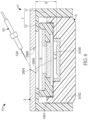
- FIG. 1 is a partial schematic cross-sectional view of a first optical detection assembly using an optical path correction subassembly provided by a first embodiment of the present disclosure
- FIG. 2 is a schematic bottom view of a first optical path correction structure of the optical path correction subassembly provided by the first embodiment of the present disclosure
- FIG. 3 is a schematic partial cross-sectional view of a second optical detection assembly using the optical path correction subassembly provided by the first embodiment of the present disclosure (when a predetermined light beam provided by an optical probe assembly cannot be guided to a light receiving surface of a light detector);
- FIG. 4 is a partial schematic cross-sectional view of the second optical detection assembly using the optical path correction subassembly provided by the first embodiment of the present disclosure (when the predetermined light beam provided by the optical probe assembly can be guided to the light receiving surface of the light detector);
- FIG. 5 is a partial schematic cross-sectional view of a third optical detection assembly using the optical path correction subassembly provided by the first embodiment of the present disclosure (when the predetermined light beam provided by the optical probe assembly cannot be guided to the light receiving surface of the light detector);
- FIG. 6 is a partial schematic cross-sectional view of the third optical detection assembly using the optical path correction subassembly provided by the first embodiment of the present disclosure (when the predetermined light beam provided by the optical probe assembly can be guided to the light receiving surface of the light detector);
- FIG. 7 is a partial schematic cross-sectional view of a fourth optical detection assembly using the optical path correction subassembly provided by the first embodiment of the present disclosure (when the predetermined light beam provided by the optical probe assembly cannot be guided to the light receiving surface of the light detector);
- FIG. 8 is a partial schematic cross-sectional view of the fourth optical detection assembly using the optical path correction subassembly provided by the first embodiment of the present disclosure (when the predetermined light beam provided by the optical probe assembly can be guided to the light receiving surface of the light detector);
- FIG. 9 is a schematic bottom view of a second optical path correction structure of the optical path correction subassembly provided by the first embodiment of the present disclosure.
- FIG. 10 is a schematic bottom view of a third optical path correction structure of the optical path correction subassembly provided by the first embodiment of the present disclosure.
- FIG. 11 is a schematic bottom view of a fourth optical path correction structure of the optical path correction subassembly provided by the first embodiment of the present disclosure.
- FIG. 12 is a schematic bottom view of a fifth optical path correction structure of the optical path correction subassembly provided by the first embodiment of the present disclosure
- FIG. 13 is a schematic bottom view of a sixth optical path correction structure of the optical path correction subassembly provided by the first embodiment of the present disclosure
- FIG. 14 is a schematic bottom view of a seventh optical path correction structure of the optical path correction subassembly provided by the first embodiment of the present disclosure
- FIG. 15 is a schematic bottom view of an eighth optical path correction structure of the optical path correction subassembly provided by the first embodiment of the present disclosure.
- FIG. 16 is a partial schematic cross-sectional view of a fifth optical detection assembly using the optical path correction subassembly provided by the first embodiment of the present disclosure
- FIG. 17 is a partial schematic cross-sectional view of an optical detection system using the optical detection assembly provided by a second embodiment of the present disclosure (when the optical probe assembly is configured to be disposed above a chuck for optically detecting a predetermined object);
- FIG. 18 is a partial schematic cross-sectional view of the optical detection system using the optical detection assembly provided by the second embodiment of the present disclosure (when an optical probe assembly needs to be moved to a position above the optical detection assembly to perform optical detection through the optical detection assembly);
- FIG. 19 is a partial schematic cross-sectional view of the optical detection system using the optical detection assembly provided by the second embodiment of the present disclosure (when another optical probe assembly needs to be moved to another position above the optical detection assembly to perform optical detection through the optical detection assembly).
- Numbering terms such as “first,” “second” or “third” can be used to describe various components, signals or the like, which are for distinguishing one component/signal from another one only, and are not intended to, nor should be construed to impose any substantive limitations on the components, signals or the like.
- a first embodiment of the present disclosure provides an optical detection assembly S 1 including a light detector D and an optical path correction subassembly C (or an optical path adjustment subassembly), in which as shown in FIG. 1 , the light detector D has a light receiving surface D 100 (such as a light receiving surface provided by a photodiode), and the optical path correction subassembly C includes a holder structure 1 detachably disposed on the light detector D and an optical path correction structure 2 (or an optical path adjustment structure 2 ) carried by the holder structure 1 .
- the optical path correction subassembly C can be optionally configured to be applied to the light detector D according to different requirements.
- the holder structure 1 includes a matching portion 11 and a carrying portion 12 disposed on the matching portion 11 , in which the matching portion 11 of the holder structure 1 can be configured to cooperate with the light detector D, and the carrying portion 12 of the holder structure 1 can be configured to carry the optical path correction structure 2 .
- the matching portion 11 and the light detector D can be moved or rotated with each other, and the optical path correction structure 2 can be detachably or fixedly disposed outside the holder structure 1 and located on a top side of the holder structure 1 (as shown in FIG. 1 ), or the optical path correction structure 2 can be detachably or fixedly disposed inside the holder structure 1 and surrounded by the holder structure 1 .
- the aforementioned details are disclosed for exemplary purposes only, and are not meant to limit the scope of the present disclosure.
- the optical path correction structure 2 has a light beam guiding surface 2000 arranged as a reverse inclination facing the light receiving surface D 100 of the light detector D in a vertical direction, and the optical path correction structure 2 has a through opening 2001 for accommodating the light beam guiding surface 2000 . That is to say, as shown in FIG. 1 , the optical path correction structure 2 has a light beam guiding surface 2000 arranged as a reverse inclination inclined relative to a vertical line V, the light beam guiding surface 2000 can be inclined counterclockwise with respect to the vertical line V, and the perpendicular projection of the light beam guiding surface 2000 can be projected onto the light receiving surface D 100 of the light detector D.
- the optical path correction structure 2 has an upper surface 2002 , a lower surface 2003 opposite to the upper surface 2002 , a top connecting interface 2004 (i.e., a topmost side of the light beam guiding surface 2000 ) connected between the upper surface 2002 and the light beam guiding surface 2000 , and a bottom connecting interface 2005 (i.e., a bottommost side of the light beam guiding surface 2000 ) connected between the lower surface 2003 and the light beam guiding surface 2000 , and the top connecting interface 2004 and the bottom connecting interface 2005 can directly face the light detector D in a perpendicular direction (that is to say, both the perpendicular projection of the top connecting interface 2004 and the perpendicular projection of the bottom connecting interface 2005 can be projected onto the light receiving surface D 100 of the light detector D).
- a perpendicular direction that is to say, both the perpendicular projection of the top connecting interface 2004 and the perpendicular projection of the bottom connecting interface 2005 can be projected onto the light receiving surface D 100 of the light detector D.
- the top connecting interface 2004 is closer to a center line of the through opening 2001 than the bottom connecting interface 2005 , and the top connecting interface 2004 is closer to a center line of the light detector D than the bottom connecting interface 2005 .
- the light beam guiding surface 2000 can be provided by an optical coating layer that is additionally formed (for example, by coating, electroplating, vapor deposition or any forming method) on the optical path correction structure 2 (that is to say, the optical path correction structure 2 includes an optical coating layer having a light beam guiding surface 2000 ), or the light beam guiding surface 2000 can be provided by a material surface layer that is possessed by the optical path correction structure 2 itself (that is to say, the material surface layer of the optical path correction structure 2 has a light beam guiding surface 2000 ).
- the aforementioned details are disclosed for exemplary purposes only, and are not meant to limit the scope of the present disclosure.
- the light beam guiding surface 2000 of the optical path correction structure 2 is arranged at an acute angle ⁇ relative to the light receiving surface D 100 of the light detector D. Therefore, as shown in FIG. 1 , when the holder structure 1 is optionally configured to be detachably disposed on the light detector D, the light beam guiding surface 2000 of the optical path correction structure 2 can be configured to effectively or accurately reflect (or guide, direct, transmit) a predetermined light beam B provided by the optical probe assembly S 3 to the light receiving surface D 100 of the light detector D so as to collect the predetermined light beam B by the light receiving surface D 100 of the light detector D.
- the light beam guiding surface 2000 of the optical path correction structure 2 can be configured to be located on an optical path between an optical probe assembly S 3 for providing the predetermined light beam B and the light receiving surface D 100 of the light detector D, so that the light beam guiding surface 2000 of the optical path correction structure 2 can be configured to effectively or accurately reflect (or guide, direct, transmit) the predetermined light beam B provided by the optical probe assembly S 3 to the light receiving surface D 100 of the light detector D so as to collect the predetermined light beam B by the light receiving surface D 100 of the light detector D.
- a relative perpendicular height H of the light beam guiding surface 2000 of the optical path correction structure 2 relative to the light receiving surface D 100 of the light detector D is adjustable.
- the relative perpendicular height H can be defined as a distance between the bottom connecting interface 2005 of the light beam guiding surface 2000 and the light receiving surface D 100 of the light detector D (as shown in FIG. 3 to FIG. 6 ), or the relative perpendicular height H can also be defined as a distance between the top connecting interface 2004 of the light beam guiding surface 2000 and the light receiving surface D 100 of the light detector D.
- the relative perpendicular height H can also be defined as a distance between any reference point provided by the light beam guiding surface 2000 and the light receiving surface D 100 of the light detector D.
- the aforementioned details are disclosed for exemplary purposes only, and are not meant to limit the scope of the present disclosure.
- the holder structure 1 when the holder structure 1 is optionally configured to be adjustably disposed on different predetermined positions of the light detector D through at least one fixing element F (such as a bolt, a screw nail or any kind of fixing element), the relative perpendicular height H of the light beam guiding surface 2000 of the optical path correction structure 2 relative to the light receiving surface D 100 of the light detector D can be adjustable according to the holder structure 1 that can be adjustably disposed on the different predetermined positions of the light detector D. More particularly, when the at least one fixing element F passes through at least one side through hole 1000 of the holder structure 1 to cooperate with one of a plurality of matching holes D 101 of the light detector D (for example, FIG.
- the holder structure 1 can be adjustably disposed on the different predetermined positions of the light detector D by cooperation of the at least one fixing element F and the matching holes D 101 , so that the holder structure 1 can be configured to adjust the relative perpendicular height H of the light beam guiding surface 2000 of the optical path correction structure 2 relative to the light receiving surface D 100 of the light detector D by cooperation of the at least one fixing element F and the matching holes D 101 .
- the relative perpendicular height H of the light beam guiding surface 2000 of the optical path correction structure 2 relative to the light receiving surface D 100 of the light detector D can be adjustable (for example, the relative perpendicular height H shown in FIG. 3 can be adjusted to the relative perpendicular height H shown in FIG.
- the light beam guiding surface 2000 of the optical path correction structure 2 can be configured to effectively or accurately reflect (or guide, direct, transmit) the predetermined light beam B provided by the optical probe assembly S 3 to the light receiving surface D 100 of the light detector D so as to collect the predetermined light beam B by the light receiving surface D 100 of the light detector D.
- the matching holes D 101 may not be required, that is to say, the fixing element F may be directly screwed to the wall of the light detector D, thereby realizing stepless adjustment.
- the aforementioned details are disclosed for exemplary purposes only, and are not meant to limit the scope of the present disclosure.
- the relative perpendicular height H of the light beam guiding surface 2000 of the optical path correction structure 2 relative to the light receiving surface D 100 of the light detector D can be adjustable according to the holder structure 1 that can be adjustably disposed on the different predetermined positions of the light detector D. More particularly, when an inner thread 1001 of the holder structure 1 and an outer thread D 102 of the light detector D cooperate with each other (For example, FIG.
- the holder structure 1 can be adjustably disposed on the different predetermined positions of the light detector D by cooperation of the inner thread 1001 of the holder structure 1 and the outer thread D 102 of the light detector D, so that the holder structure 1 can be configured to adjust the relative perpendicular height H of the light beam guiding surface 2000 of the optical path correction structure 2 relative to the light receiving surface D 100 of the light detector D by cooperation of the inner thread 1001 of the holder structure 1 and the outer thread D 102 of the light detector D.
- the relative perpendicular height H of the light beam guiding surface 2000 of the optical path correction structure 2 relative to the light receiving surface D 100 of the light detector D can be adjustable (for example, the relative perpendicular height H shown in FIG. 5 can be adjusted to the relative perpendicular height H shown in FIG.
- the light beam guiding surface 2000 of the optical path correction structure 2 can be configured to effectively or accurately reflect (or guide, direct, transmit) the predetermined light beam B provided by the optical probe assembly S 3 to the light receiving surface D 100 of the light detector D so as to collect the predetermined light beam B by the light receiving surface D 100 of the light detector D.
- the aforementioned details are disclosed for exemplary purposes only, and are not meant to limit the scope of the present disclosure.
- the relative perpendicular height H of the light beam guiding surface 2000 of the optical path correction structure 2 relative to the light receiving surface D 100 of the light detector D can be adjustable, so that in the case where the orientation of the light detector D (such as using a photodiode) provided by the present disclosure does not need to be adjusted by an external adjustment mechanism, the light detector D can still be used to optically detect the quality of an optical probe S 30 (i.e., an optical fiber) of the optical probe assembly S 3 arranged in different orientations (such as different angles and/or heights) by use of the optical path correction subassembly C having a light beam guiding surface 2000 for effectively or accurately reflecting (or guiding, directing, transmitting) a predetermined light beam B provided by the optical probe S 30 of the optical probe assembly S 3 to a light receiving surface D 100 of the light detector D.
- an optical probe S 30 i.e., an optical fiber
- the optical path correction subassembly C having a light beam guiding surface 2000 for effectively or accurately reflecting (
- the present disclosure can automatically detect the quality of the optical probe S 30 of the optical probe assembly S 3 by use of the optical path correction subassembly C having the light beam guiding surface 2000 without the assistance of the external adjustment mechanism, so as to simplify the mechanical structure and achieve the advantage of reducing cost.
- the holder structure 1 can be adjustably disposed on the different predetermined positions of the light detector D by cooperation of the at least one fixing element F and the matching holes D 101 , so that the holder structure 1 can be configured to adjust the relative perpendicular height H of the light beam guiding surface 2000 of the optical path correction structure 2 relative to the light receiving surface D 100 of the light detector D by cooperation of the at least one fixing element F and the matching holes D 101 (It should be noted that the at least one fixing element F can be operated through the user's hand or a screwdriver, but both the user's hand or the screwdriver are used to provide a power source to drive the at least one fixing element F rather than the external adjustment mechanism).
- the holder structure 1 can be adjustably disposed on the different predetermined positions of the light detector D by cooperation of the inner thread 1001 of the holder structure 1 and the outer thread D 102 of the light detector D, so that the holder structure 1 can be configured to adjust the relative perpendicular height H of the light beam guiding surface 2000 of the optical path correction structure 2 relative to the light receiving surface D 100 of the light detector D by cooperation of the inner thread 1001 of the holder structure 1 and the outer thread D 102 of the light detector D.
- a relative inclination angle of the light beam guiding surface 2000 of the optical path correction structure 2 relative to the light receiving surface D 100 of the light detector D can be adjustable.
- FIG. 7 shows that the beam guiding surface 2000 of the optical path correction structure 2 is inclined with respect to the light receiving surface D 100 of the light detector D to present a relative inclination angle ⁇ 1
- FIG. 8 shows that the beam guiding surface 2000 of the optical path correction structure 2 is inclined with respect to the light receiving surface D 100 of the light detector D to present a relative inclination angle ⁇ 1 , and FIG.
- the beam guiding surface 2000 of the optical path correction structure 2 is inclined with respect to the light receiving surface D 100 of the light detector D to present a relative inclination angle ⁇ 2 .
- the relative inclination angle ⁇ 1 and the relative inclination angle ⁇ 2 could be inclined with respect to the upper surface 2002 or the lower surface 2003 of the optical path correction structure 2 .
- the aforementioned details are disclosed for exemplary purposes only, and are not meant to limit the scope of the present disclosure.
- the optical path correction structure 2 includes a one-piece optical element (as shown in FIG. 2 ) or a combined-type optical element composed of a plurality of optical matching parts 20 S (as shown in FIG. 9 , the combined-type optical element can be composed of three optical matching parts 20 S).
- the optical path correction subassembly C when the optical path correction subassembly C is optionally configured to be replaceably disposed on the light detector D (or when the optical path correction structure 2 can be configured to be replaceably disposed on the holder structure 1 ), the optical path correction subassembly C (i.e., the optical path correction structure 2 ) can be replaced by a plurality of different one-piece optical elements or a plurality of different combined-type optical elements (for example, the light beam guiding surfaces 2000 of the different one-piece optical elements have different inclination angles, respectively, or the light beam guiding surfaces 2000 of the different combined-type optical elements have different inclination angles, respectively), so that the relative inclination angle of the light beam guiding surface 2000 of the optical path correction structure 2 relative to the light receiving surface D 100 of the light detector D can be adjustable or choiceful.
- the relative inclination angle of the light beam guiding surface 2000 of the optical path correction structure 2 relative to the light receiving surface D 100 of the light detector D can be adjustable (for example, the relative inclination angle ⁇ 1 of the beam guiding surface 2000 relative to the light receiving surface D 100 as shown in FIG. 7 is greater than the relative inclination angle ⁇ 2 of the beam guiding surface 2000 relative to the light receiving surface D 100 as shown in FIG.
- the light beam guiding surface 2000 of the optical path correction structure 2 can be configured to effectively or accurately reflect (or guide, direct, transmit) the predetermined light beam B provided by the optical probe assembly S 3 to the light receiving surface D 100 of the light detector D so as to collect the predetermined light beam B by the light receiving surface D 100 of the light detector D.
- the aforementioned details are disclosed for exemplary purposes only, and are not meant to limit the scope of the present disclosure.
- the optical path correction structure 2 has a through opening 2001 for accommodating the light beam guiding surface 2000
- the through opening 2001 can be shaped as a closed shape (such as a circle shown in FIG. 2 , a square or any closed shape) or an open shape (such as a 1 ⁇ 2 circle shown in FIG. 10 , a 3 ⁇ 4 circle shown in FIG. 11 , or any open shape)
- the through opening 2001 can be provided by the one-piece optical element (as shown in FIG. 1 ) or can be formed by combining the optical matching parts 20 S of the combined-type optical element (as shown in FIG. 9 ).
- the number of the through opening 2001 provided by the present disclosure may not only be one as shown in FIG. 2 and FIG. 10 , for example, the number of the through opening 2001 disclosed in FIG. 12 and FIG. 13 may also be multiple, and the plurality of light beam guiding surface 2000 may have the same or different inclination angles.
- the optical path correction structure 2 has a strip-shaped beam guiding surface 2000 and an open-type through opening 2001 adjacent to the strip-shaped beam guiding surface 2000 (as shown in FIG. 14 ), or the optical path correction structure 2 has at least two strip-shaped beam guiding surfaces 2000 and a through opening 2001 located between the two strip-shaped beam guiding surfaces 2000 (as shown in FIG. 15 ).
- the aforementioned details are disclosed for exemplary purposes only, and are not meant to limit the scope of the present disclosure.
- the through opening 2001 has a topmost opening 2001 P and a bottommost opening 2011 B, and a size of the topmost opening 2001 P is smaller than a size of the bottommost opening 2011 B.
- the size of the topmost opening 2001 P and the size of the bottommost opening 2011 B have a proportional relationship within a predetermined range, so that the relative inclination angle of the light beam guiding surface 2000 of the optical path correction structure 2 relative to the light receiving surface D 100 of the light detector D can be adjustable.
- the relative inclination angle of the light beam guiding surface 2000 of the optical path correction structure 2 with respect to the light receiving surface D 100 of the light detector D is larger.
- the light beam guiding surface 2000 of the optical path correction structure 2 has a plurality of light beam guiding regions 2000 R, and the light beam guiding regions 2000 R can be configured to be disposed on the one-piece optical element (as shown in FIG. 2 , three light beam guiding regions 2000 R are distributed on the light beam guiding surface 2000 ) or configured to be respectively disposed on the optical matching parts 20 S of the combined-type optical element (as shown in FIG. 9 , three light beam guiding regions 2000 R are respectively formed on the three optical matching parts 20 S), and the light beam guiding regions 2000 R have a same inclination angle or different inclination angles relative to the vertical line V.
- the relative inclination angle of the light beam guiding surface 2000 of the optical path correction structure 2 relative to the light receiving surface D 100 of the light detector D can be adjustable by virtue of “the same or different inclination angles provided by the light beam guiding regions 2000 R of the one-piece optical element” or “the same or different inclination angles provided by the light beam guiding regions 2000 R of the combined-type optical element.”
- the aforementioned details are disclosed for exemplary purposes only, and are not meant to limit the scope of the present disclosure.
- the optical probe assembly S 3 can be set very close to a horizontal plane (that is to say, the inclination angle of the optical probe assembly S 3 relative to the light receiving surface D 100 of the light detector D can be very small), so that the optical probe assembly S 3 can be used more flexibly in cooperation with the optical path correction structure 2 .
- the relative inclination angle of the light beam guiding surface 2000 of the optical path correction structure 2 relative to the light receiving surface D 100 of the light detector D is adjustable, so that in the case where the orientation of the light detector D (such as using a photodiode) provided by the present disclosure does not need to be adjusted by an external adjustment mechanism, the light detector D can still be used to optically detect the quality of an optical probe S 30 (i.e., an optical fiber) of the optical probe assembly S 3 arranged in different orientations (such as different angles and/or heights) by use of the optical path correction subassembly C having a light beam guiding surface 2000 for effectively or accurately reflecting (or guiding, directing, transmitting) a predetermined light beam B provided by the optical probe S 30 of the optical probe assembly S 3 to a light receiving surface D 100 of the light detector D.
- an optical probe S 30 i.e., an optical fiber
- the optical path correction subassembly C having a light beam guiding surface 2000 for effectively or accurately reflecting (or guiding
- the present disclosure can automatically detect the quality of the optical probe S 30 of the optical probe assembly S 3 by use of the optical path correction subassembly C having the light beam guiding surface 2000 without the assistance of the external adjustment mechanism, so as to simplify the mechanical structure and achieve the advantage of reducing cost.
- the present disclosure can adjust the relative inclination angle of the light beam guiding surface 2000 of the optical path correction structure 2 relative to the light receiving surface D 100 of the light detector D through the following different method so as to meet the different customized requirements.
- the different methods for adjusting the relative inclination angle can be at least one or more of the following possible solutions: (1) the optical path correction structure 2 can be a one-piece optical element or a combined-type optical element composed of a plurality of optical matching parts 20 S; (2) the through opening 2001 can be provided by the one-piece optical element or can be formed by combining the optical matching parts 20 S of the combined-type optical element; (3) for the through opening 2001 , the size of the topmost opening 2001 P can be smaller than the size of the bottommost opening 2011 B, and the size of the topmost opening 2001 P and the size of the bottommost opening 2011 B have a proportional relationship within a predetermined range; and (4) the light beam guiding regions 2000 R can be configured to be disposed on the one-piece optical element or configured to be respectively disposed on the optical matching parts 20 S of the combined-type optical element, and the light beam guiding regions 2000 R have a same inclination angle or different inclination angles relative to a vertical line V.
- the optical path correction structure 2 has a light beam guiding surface 2000 arranged as a reverse inclination facing the light receiving surface D 100 of the light detector D in a vertical direction (that is to say, the optical path correction structure 2 has a light beam guiding surface 2000 arranged as a reverse inclination inclined relative to a vertical line V), and the light beam guiding surface 2000 of the optical path correction structure 2 is arranged at an acute angle ⁇ relative to the light receiving surface D 100 of the light detector D, so that when the holder structure 1 is optionally configured to be detachably disposed on the light detector D, the light beam guiding surface 2000 of the optical path correction structure 2 can be configured to guide a predetermined light beam B to the light receiving surface D 100 of the light detector D so as to effectively or accurately collect the predetermined light beam B by the light receiving surface D 100 of the light detector D.
- the light detector D can still be used to optically detect the quality of the optical probe S 30 (i.e., an optical fiber) of an optical probe assembly S 3 arranged in different orientations (such as different angles and/or heights) by use of the optical path correction subassembly C having a light beam guiding surface 2000 (for example, at least one of the relative perpendicular height H and the relative inclination angle of the light beam guiding surface 2000 of the optical path correction structure 2 relative to the light receiving surface D 100 of the light detector D is adjustable) for guiding a predetermined light beam B to a light receiving surface D 100 of the light detector D.
- the optical path correction subassembly C having a light beam guiding surface 2000 (for example, at least one of the relative perpendicular height H and the relative inclination angle of the light beam guiding surface 2000 of the optical path correction structure 2 relative to the light receiving surface D 100 of the light detector D is adjustable) for guiding a predetermined light beam B to a light receiving surface D 100 of the light detector D
- the present disclosure can automatically detect the quality of the optical probe S 30 of the optical probe assembly S 3 by use of the optical path correction subassembly C having the light beam guiding surface 2000 without the assistance of the external adjustment mechanism, so as to simplify the mechanical structure and achieve the advantage of reducing cost.
- a second embodiment of the present disclosure provides an optical detection system S including an optical detection assembly S 1 (can be provided by the first embodiment), a chuck stage S 2 and two optical probe assemblies S 3 (or using only one optical probe assembly S 3 ).
- the chuck stage S 2 includes a chuck S 20 for carrying a plurality of predetermined objects W (such as wafer having a plurality of chips).
- the optical probe assembly S 3 can be configured to be disposed above the chuck S 20 for optically detecting the predetermined object W (as shown in FIG. 17 ).
- the optical detection assembly S 1 can be configured adjacent to the chuck S 20 of the chuck stage S 2 for optically detecting a predetermined light beam B provided by the optical probe assembly S 3 .
- the optical detection assembly S 1 includes a light detector D and an optical path correction subassembly C
- the light detector D has a light receiving surface D 100
- the optical path correction subassembly C includes a holder structure 1 detachably disposed on the light detector D and an optical path correction structure 2 carried by the holder structure 1 .
- the optical path correction structure 2 has a light beam guiding surface 2000 arranged as a reverse inclination facing the light receiving surface D 100 of the light detector D in a vertical direction, the light beam guiding surface 2000 of the optical path correction structure 2 is arranged at an acute angle ⁇ relative to the light receiving surface D 100 of the light detector D, and the light beam guiding surface 2000 of the optical path correction structure 2 can be configured to guide the predetermined light beam B to a light receiving surface D 100 of the light detector D so as to facilitate collection of the predetermined light beam B.
- an upper surface 2002 of the optical path correction structure 2 of the optical path correction subassembly C can be equal to or lower than the wafer carrying surface S 2000 of the chuck S 20 of the chuck stage S 2 so as to prevent the optical probe assembly S 3 from being touched or collided by the optical path correction subassembly C.
- FIG. 18 when one of the two optical probe assemblies S 3 (such as the optical probe assembly S 3 located on the right side of FIG.
- the optical probe assembly S 3 located on the right side of FIG. 18 will not collide with the optical detection assembly S 1 during the movement.
- FIG. 19 when another one of the two optical probe assemblies S 3 (such as the optical probe assembly S 3 located on the left side of FIG.
- the optical probe assembly S 3 located on the left side of FIG. 19 will not collide with the optical detection assembly S 1 during the movement.
- the optical probe assembly S 3 can be returned to a position above the chuck S 20 for optically detecting the predetermined object W.
- the entire optical detection assembly S 1 can be located at a lower position than the entire chuck stage S 2 or at the same height as the entire wafer table (that is to say, the upper surface 2002 of the optical path correction structure 2 can be equal to or lower than the wafer carrying surface S 2000 of the chuck stage S 2 ), so that the optical probe S 30 of the optical probe assembly S 3 adjacent to the optical detection assembly S 1 will not collide with the relatively low optical detection assembly S 1 during the movement, and another optical probe S 30 of the optical probe assembly S 3 far from the optical detection assembly S 1 will not be blocked by the relatively low optical detection assembly S 1 and can be optically detected by the same light detector D. That is to say, there is only a relative horizontal movement between the optical probe assembly S 3 and the chuck S 20 , so that even if detecting the quality of the optical probe S 30 of the optical probe assembly S 3 is frequent, the efficiency of detection is improved.
Landscapes
- Physics & Mathematics (AREA)
- Chemical & Material Sciences (AREA)
- Analytical Chemistry (AREA)
- General Physics & Mathematics (AREA)
- Optics & Photonics (AREA)
- Biochemistry (AREA)
- Life Sciences & Earth Sciences (AREA)
- General Health & Medical Sciences (AREA)
- Health & Medical Sciences (AREA)
- Immunology (AREA)
- Pathology (AREA)
- Dispersion Chemistry (AREA)
- Optical Couplings Of Light Guides (AREA)
- Photometry And Measurement Of Optical Pulse Characteristics (AREA)
- Geophysics And Detection Of Objects (AREA)
Abstract
Description
Claims (15)
Priority Applications (1)
| Application Number | Priority Date | Filing Date | Title |
|---|---|---|---|
| US17/979,748 US12007319B2 (en) | 2021-11-08 | 2022-11-02 | Optical path correction subassembly, optical detection assembly, and optical detection system |
Applications Claiming Priority (2)
| Application Number | Priority Date | Filing Date | Title |
|---|---|---|---|
| US202163276671P | 2021-11-08 | 2021-11-08 | |
| US17/979,748 US12007319B2 (en) | 2021-11-08 | 2022-11-02 | Optical path correction subassembly, optical detection assembly, and optical detection system |
Publications (2)
| Publication Number | Publication Date |
|---|---|
| US20230147804A1 US20230147804A1 (en) | 2023-05-11 |
| US12007319B2 true US12007319B2 (en) | 2024-06-11 |
Family
ID=86053078
Family Applications (1)
| Application Number | Title | Priority Date | Filing Date |
|---|---|---|---|
| US17/979,748 Active US12007319B2 (en) | 2021-11-08 | 2022-11-02 | Optical path correction subassembly, optical detection assembly, and optical detection system |
Country Status (3)
| Country | Link |
|---|---|
| US (1) | US12007319B2 (en) |
| DE (1) | DE102022129095A1 (en) |
| TW (1) | TWI836694B (en) |
Citations (4)
| Publication number | Priority date | Publication date | Assignee | Title |
|---|---|---|---|---|
| US5642056A (en) * | 1993-12-22 | 1997-06-24 | Tokyo Electron Limited | Probe apparatus for correcting the probe card posture before testing |
| US7871810B2 (en) * | 2004-11-03 | 2011-01-18 | Life Technologies Corporation | Multiaxis focusing mechanism for microarray analysis |
| US20170322133A1 (en) * | 2004-03-06 | 2017-11-09 | Michael Trainer | Methods and apparatus for determining particle characteristics by utilizing force on particles |
| CN112444923A (en) | 2019-08-30 | 2021-03-05 | 青岛海信宽带多媒体技术有限公司 | Optical module |
Family Cites Families (2)
| Publication number | Priority date | Publication date | Assignee | Title |
|---|---|---|---|---|
| US7130039B2 (en) * | 2002-04-18 | 2006-10-31 | Kla-Tencor Technologies Corporation | Simultaneous multi-spot inspection and imaging |
| US11300525B2 (en) * | 2019-07-31 | 2022-04-12 | Taiwan Semiconductor Manufacturing Company, Ltd. | Wafer inspection apparatus and method |
-
2022
- 2022-11-02 TW TW111141710A patent/TWI836694B/en active
- 2022-11-02 US US17/979,748 patent/US12007319B2/en active Active
- 2022-11-03 DE DE102022129095.6A patent/DE102022129095A1/en active Pending
Patent Citations (4)
| Publication number | Priority date | Publication date | Assignee | Title |
|---|---|---|---|---|
| US5642056A (en) * | 1993-12-22 | 1997-06-24 | Tokyo Electron Limited | Probe apparatus for correcting the probe card posture before testing |
| US20170322133A1 (en) * | 2004-03-06 | 2017-11-09 | Michael Trainer | Methods and apparatus for determining particle characteristics by utilizing force on particles |
| US7871810B2 (en) * | 2004-11-03 | 2011-01-18 | Life Technologies Corporation | Multiaxis focusing mechanism for microarray analysis |
| CN112444923A (en) | 2019-08-30 | 2021-03-05 | 青岛海信宽带多媒体技术有限公司 | Optical module |
Also Published As
| Publication number | Publication date |
|---|---|
| US20230147804A1 (en) | 2023-05-11 |
| TW202319729A (en) | 2023-05-16 |
| TWI836694B (en) | 2024-03-21 |
| DE102022129095A1 (en) | 2023-05-11 |
Similar Documents
| Publication | Publication Date | Title |
|---|---|---|
| US5068912A (en) | Track gauges for aligning and focussing the imaging system in a high speed document handling system | |
| US6900451B2 (en) | Mapping sensor system for detecting positions of flat objects | |
| US4786816A (en) | Wafer detecting device wherein light receiver has an effective surface larger than the dimensional range covering all the wafers being detected | |
| US12007319B2 (en) | Optical path correction subassembly, optical detection assembly, and optical detection system | |
| US7889326B2 (en) | Distance measuring apparatus | |
| CA3218672A1 (en) | Method for testing at least one battery cell stack with regard to the position of battery cell layers | |
| CN104501946B (en) | System and method for measuring high-strength beam | |
| US20040136100A1 (en) | Optical sensor | |
| US20040043514A1 (en) | Pre-aligner | |
| US20030141465A1 (en) | Semiconductor wafer carrier mapping sensor | |
| US6194713B1 (en) | Scanning optical device having a rotatable adjustable holder | |
| CN120453851B (en) | Coupling equipment and coupling method for reflecting mirror in pump body | |
| US20100165346A1 (en) | Apparatus for detecting a sample | |
| CN207408735U (en) | A kind of detection device and camera module detection device | |
| EP0481515A2 (en) | Illumination system for scanner | |
| CN219455307U (en) | A kind of optical path calibration module | |
| CN113702007B (en) | A calibration device for off-axis beam axis difference and its calibration method | |
| JP5196400B2 (en) | Specific gravity measuring device for liquid sample | |
| CN214953086U (en) | Detection device | |
| CN108120683A (en) | Adjustable light source device for biochemical analyzer | |
| US5448415A (en) | Device for emitting light diverging along imaginary plane | |
| CN218743325U (en) | High efficiency silicon chip warpage detection device | |
| CN217370918U (en) | Vibrating mirror type optical path system with calibration function | |
| TWI824565B (en) | Optical detection system and integrated optical detection device | |
| US10969577B2 (en) | Optical scanning equipment |
Legal Events
| Date | Code | Title | Description |
|---|---|---|---|
| AS | Assignment |
Owner name: MPI CORPORATION, TAIWAN Free format text: ASSIGNMENT OF ASSIGNORS INTEREST;ASSIGNORS:TING, PO-YI;YEN, TING-AN;HSU, YU-HSUN;AND OTHERS;SIGNING DATES FROM 20220926 TO 20221031;REEL/FRAME:061638/0291 |
|
| FEPP | Fee payment procedure |
Free format text: ENTITY STATUS SET TO UNDISCOUNTED (ORIGINAL EVENT CODE: BIG.); ENTITY STATUS OF PATENT OWNER: LARGE ENTITY |
|
| STPP | Information on status: patent application and granting procedure in general |
Free format text: DOCKETED NEW CASE - READY FOR EXAMINATION |
|
| STPP | Information on status: patent application and granting procedure in general |
Free format text: NON FINAL ACTION MAILED |
|
| STPP | Information on status: patent application and granting procedure in general |
Free format text: RESPONSE TO NON-FINAL OFFICE ACTION ENTERED AND FORWARDED TO EXAMINER |
|
| STPP | Information on status: patent application and granting procedure in general |
Free format text: FINAL REJECTION MAILED |
|
| STPP | Information on status: patent application and granting procedure in general |
Free format text: RESPONSE AFTER FINAL ACTION FORWARDED TO EXAMINER |
|
| STPP | Information on status: patent application and granting procedure in general |
Free format text: NOTICE OF ALLOWANCE MAILED -- APPLICATION RECEIVED IN OFFICE OF PUBLICATIONS |
|
| STPP | Information on status: patent application and granting procedure in general |
Free format text: PUBLICATIONS -- ISSUE FEE PAYMENT VERIFIED |
|
| STCF | Information on status: patent grant |
Free format text: PATENTED CASE |