US11894242B2 - Semiconductor package and method of manufacturing semiconductor package - Google Patents
Semiconductor package and method of manufacturing semiconductor package Download PDFInfo
- Publication number
- US11894242B2 US11894242B2 US18/174,576 US202318174576A US11894242B2 US 11894242 B2 US11894242 B2 US 11894242B2 US 202318174576 A US202318174576 A US 202318174576A US 11894242 B2 US11894242 B2 US 11894242B2
- Authority
- US
- United States
- Prior art keywords
- substrate
- semiconductor chip
- reinforcing pattern
- molding material
- mechanical reinforcing
- Prior art date
- Legal status (The legal status is an assumption and is not a legal conclusion. Google has not performed a legal analysis and makes no representation as to the accuracy of the status listed.)
- Active
Links
Images


Classifications
-
- H10W74/016—
-
- H10W42/121—
-
- H—ELECTRICITY
- H01—ELECTRIC ELEMENTS
- H01L—SEMICONDUCTOR DEVICES NOT COVERED BY CLASS H10
- H01L21/00—Processes or apparatus adapted for the manufacture or treatment of semiconductor or solid state devices or of parts thereof
- H01L21/02—Manufacture or treatment of semiconductor devices or of parts thereof
- H01L21/04—Manufacture or treatment of semiconductor devices or of parts thereof the devices having potential barriers, e.g. a PN junction, depletion layer or carrier concentration layer
- H01L21/50—Assembly of semiconductor devices using processes or apparatus not provided for in a single one of the groups H01L21/18 - H01L21/326 or H10D48/04 - H10D48/07 e.g. sealing of a cap to a base of a container
- H01L21/56—Encapsulations, e.g. encapsulation layers, coatings
- H01L21/565—Moulds
-
- H—ELECTRICITY
- H01—ELECTRIC ELEMENTS
- H01L—SEMICONDUCTOR DEVICES NOT COVERED BY CLASS H10
- H01L23/00—Details of semiconductor or other solid state devices
- H01L23/16—Fillings or auxiliary members in containers or encapsulations, e.g. centering rings
- H01L23/18—Fillings characterised by the material, its physical or chemical properties, or its arrangement within the complete device
- H01L23/24—Fillings characterised by the material, its physical or chemical properties, or its arrangement within the complete device solid or gel at the normal operating temperature of the device
-
- H10W74/00—
-
- H10W76/40—
-
- H10W76/47—
-
- H—ELECTRICITY
- H01—ELECTRIC ELEMENTS
- H01L—SEMICONDUCTOR DEVICES NOT COVERED BY CLASS H10
- H01L21/00—Processes or apparatus adapted for the manufacture or treatment of semiconductor or solid state devices or of parts thereof
- H01L21/02—Manufacture or treatment of semiconductor devices or of parts thereof
- H01L21/04—Manufacture or treatment of semiconductor devices or of parts thereof the devices having potential barriers, e.g. a PN junction, depletion layer or carrier concentration layer
- H01L21/50—Assembly of semiconductor devices using processes or apparatus not provided for in a single one of the groups H01L21/18 - H01L21/326 or H10D48/04 - H10D48/07 e.g. sealing of a cap to a base of a container
- H01L21/56—Encapsulations, e.g. encapsulation layers, coatings
- H01L21/561—Batch processing
-
- H—ELECTRICITY
- H01—ELECTRIC ELEMENTS
- H01L—SEMICONDUCTOR DEVICES NOT COVERED BY CLASS H10
- H01L2224/00—Indexing scheme for arrangements for connecting or disconnecting semiconductor or solid-state bodies and methods related thereto as covered by H01L24/00
- H01L2224/01—Means for bonding being attached to, or being formed on, the surface to be connected, e.g. chip-to-package, die-attach, "first-level" interconnects; Manufacturing methods related thereto
- H01L2224/10—Bump connectors; Manufacturing methods related thereto
- H01L2224/15—Structure, shape, material or disposition of the bump connectors after the connecting process
- H01L2224/16—Structure, shape, material or disposition of the bump connectors after the connecting process of an individual bump connector
- H01L2224/161—Disposition
- H01L2224/16151—Disposition the bump connector connecting between a semiconductor or solid-state body and an item not being a semiconductor or solid-state body, e.g. chip-to-substrate, chip-to-passive
- H01L2224/16221—Disposition the bump connector connecting between a semiconductor or solid-state body and an item not being a semiconductor or solid-state body, e.g. chip-to-substrate, chip-to-passive the body and the item being stacked
- H01L2224/16225—Disposition the bump connector connecting between a semiconductor or solid-state body and an item not being a semiconductor or solid-state body, e.g. chip-to-substrate, chip-to-passive the body and the item being stacked the item being non-metallic, e.g. insulating substrate with or without metallisation
- H01L2224/16227—Disposition the bump connector connecting between a semiconductor or solid-state body and an item not being a semiconductor or solid-state body, e.g. chip-to-substrate, chip-to-passive the body and the item being stacked the item being non-metallic, e.g. insulating substrate with or without metallisation the bump connector connecting to a bond pad of the item
-
- H—ELECTRICITY
- H01—ELECTRIC ELEMENTS
- H01L—SEMICONDUCTOR DEVICES NOT COVERED BY CLASS H10
- H01L2224/00—Indexing scheme for arrangements for connecting or disconnecting semiconductor or solid-state bodies and methods related thereto as covered by H01L24/00
- H01L2224/01—Means for bonding being attached to, or being formed on, the surface to be connected, e.g. chip-to-package, die-attach, "first-level" interconnects; Manufacturing methods related thereto
- H01L2224/42—Wire connectors; Manufacturing methods related thereto
- H01L2224/47—Structure, shape, material or disposition of the wire connectors after the connecting process
- H01L2224/48—Structure, shape, material or disposition of the wire connectors after the connecting process of an individual wire connector
- H01L2224/481—Disposition
- H01L2224/48151—Connecting between a semiconductor or solid-state body and an item not being a semiconductor or solid-state body, e.g. chip-to-substrate, chip-to-passive
- H01L2224/48221—Connecting between a semiconductor or solid-state body and an item not being a semiconductor or solid-state body, e.g. chip-to-substrate, chip-to-passive the body and the item being stacked
- H01L2224/48225—Connecting between a semiconductor or solid-state body and an item not being a semiconductor or solid-state body, e.g. chip-to-substrate, chip-to-passive the body and the item being stacked the item being non-metallic, e.g. insulating substrate with or without metallisation
- H01L2224/48227—Connecting between a semiconductor or solid-state body and an item not being a semiconductor or solid-state body, e.g. chip-to-substrate, chip-to-passive the body and the item being stacked the item being non-metallic, e.g. insulating substrate with or without metallisation connecting the wire to a bond pad of the item
-
- H—ELECTRICITY
- H01—ELECTRIC ELEMENTS
- H01L—SEMICONDUCTOR DEVICES NOT COVERED BY CLASS H10
- H01L2224/00—Indexing scheme for arrangements for connecting or disconnecting semiconductor or solid-state bodies and methods related thereto as covered by H01L24/00
- H01L2224/73—Means for bonding being of different types provided for in two or more of groups H01L2224/10, H01L2224/18, H01L2224/26, H01L2224/34, H01L2224/42, H01L2224/50, H01L2224/63, H01L2224/71
- H01L2224/732—Location after the connecting process
- H01L2224/73201—Location after the connecting process on the same surface
- H01L2224/73203—Bump and layer connectors
- H01L2224/73204—Bump and layer connectors the bump connector being embedded into the layer connector
-
- H—ELECTRICITY
- H01—ELECTRIC ELEMENTS
- H01L—SEMICONDUCTOR DEVICES NOT COVERED BY CLASS H10
- H01L2224/00—Indexing scheme for arrangements for connecting or disconnecting semiconductor or solid-state bodies and methods related thereto as covered by H01L24/00
- H01L2224/73—Means for bonding being of different types provided for in two or more of groups H01L2224/10, H01L2224/18, H01L2224/26, H01L2224/34, H01L2224/42, H01L2224/50, H01L2224/63, H01L2224/71
- H01L2224/732—Location after the connecting process
- H01L2224/73251—Location after the connecting process on different surfaces
- H01L2224/73265—Layer and wire connectors
-
- H—ELECTRICITY
- H01—ELECTRIC ELEMENTS
- H01L—SEMICONDUCTOR DEVICES NOT COVERED BY CLASS H10
- H01L24/00—Arrangements for connecting or disconnecting semiconductor or solid-state bodies; Methods or apparatus related thereto
- H01L24/01—Means for bonding being attached to, or being formed on, the surface to be connected, e.g. chip-to-package, die-attach, "first-level" interconnects; Manufacturing methods related thereto
- H01L24/10—Bump connectors ; Manufacturing methods related thereto
- H01L24/15—Structure, shape, material or disposition of the bump connectors after the connecting process
- H01L24/16—Structure, shape, material or disposition of the bump connectors after the connecting process of an individual bump connector
-
- H—ELECTRICITY
- H01—ELECTRIC ELEMENTS
- H01L—SEMICONDUCTOR DEVICES NOT COVERED BY CLASS H10
- H01L24/00—Arrangements for connecting or disconnecting semiconductor or solid-state bodies; Methods or apparatus related thereto
- H01L24/01—Means for bonding being attached to, or being formed on, the surface to be connected, e.g. chip-to-package, die-attach, "first-level" interconnects; Manufacturing methods related thereto
- H01L24/42—Wire connectors; Manufacturing methods related thereto
- H01L24/47—Structure, shape, material or disposition of the wire connectors after the connecting process
- H01L24/48—Structure, shape, material or disposition of the wire connectors after the connecting process of an individual wire connector
-
- H—ELECTRICITY
- H01—ELECTRIC ELEMENTS
- H01L—SEMICONDUCTOR DEVICES NOT COVERED BY CLASS H10
- H01L24/00—Arrangements for connecting or disconnecting semiconductor or solid-state bodies; Methods or apparatus related thereto
- H01L24/73—Means for bonding being of different types provided for in two or more of groups H01L24/10, H01L24/18, H01L24/26, H01L24/34, H01L24/42, H01L24/50, H01L24/63, H01L24/71
-
- H10W72/0198—
-
- H10W72/07236—
-
- H10W72/07337—
-
- H10W72/075—
-
- H10W72/222—
-
- H10W72/354—
-
- H10W72/5522—
-
- H10W72/5524—
-
- H10W72/884—
-
- H10W74/014—
-
- H10W74/117—
-
- H10W74/15—
-
- H10W90/724—
-
- H10W90/734—
-
- H10W90/754—
Definitions
- Example embodiments relate to a semiconductors, and more particularly, to a semiconductor package and method of manufacturing a semiconductor package.
- a semiconductor package includes, a package substrate, at least one semiconductor chip mounted on the package substrate, a molding member on the package substrate to cover at least a portion of the semiconductor chip, and a mechanical reinforcing member provided around the semiconductor chip within the molding member and extending in at least one direction.
- a semiconductor package includes, a package substrate having an upper surface and a lower surface opposite to each other, at least one semiconductor chip mounted on the upper surface of the package substrate, a molding member on the upper surface of the package substrate to cover at least a portion of the semiconductor chip, and a reinforcing member provided in at least a portion of the molding member and extending around the semiconductor chip.
- a semiconductor chip is arranged on a substrate.
- the substrate is disposed in a cavity between a lower mold and an upper mold of a molding apparatus.
- a mechanical reinforcing pattern is positioned around the semiconductor chip within the cavity.
- a molding material is injected into the cavity and cured.
- a semiconductor package may include a mechanical reinforcing pattern within a molding member which covers a semiconductor chip provided on a package substrate.
- the mechanical reinforcing pattern may extend in at least one direction around the semiconductor chip within the molding member.
- the mechanical reinforcing pattern may include a material different from the molding member to serve as a mechanical reinforcing member to improve mechanical properties of the semiconductor package.
- a material, physical properties, and a size of the reinforcing pattern may be selected to prevent cracks and improve mechanical properties of the semiconductor package.
- FIGS. 1 to 14 represent non-limiting, example embodiments as described herein.
- FIG. 1 is a plan view illustrating a semiconductor package in accordance with example embodiments.
- FIG. 2 is a cross-sectional view taken along the line A-A′ in FIG. 1 .
- FIG. 3 is a cross-sectional view taken along the line B-B′ in FIG. 1 .
- FIGS. 4 to 7 are cross-sectional views illustrating a method of manufacturing a semiconductor package in accordance with example embodiments.
- FIGS. 8 to 10 are plan views illustrating a reinforcing member in accordance with example embodiments.
- FIG. 11 is a plan view illustrating a semiconductor package in accordance with example embodiments.
- FIG. 12 is a cross-sectional view taken along the line C-C′ in FIG. 11 .
- FIGS. 13 and 14 are cross-sectional views illustrating a method of manufacturing a semiconductor package in accordance with example embodiments.
- FIG. 1 is a plan view illustrating a semiconductor package in accordance with example embodiments.
- FIG. 2 is a cross-sectional view taken along the line A-A′ in FIG. 1 .
- FIG. 3 is a cross-sectional view taken along the line B-B′ in FIG. 1 .
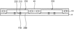
- a semiconductor package 10 may include a package substrate 100 , at least one semiconductor chip 200 arranged on an upper surface 102 of the package substrate 100 , a molding member 300 on the upper surface 102 of the package substrate 100 to cover at least a portion of the semiconductor chip 200 , and a reinforcing member extending in at least one direction within the molding member 300 .
- the semiconductor package 10 may further include outer connection members 500 disposed on a lower surface 104 of the package substrate 100 .
- the package substrate 100 may be a substrate having the upper surface 102 and the lower surface 104 opposite to each other.
- the package substrate 100 may be a printed circuit board (PCB).
- the PCB may be a multilayered circuit board, and may include vias and various circuits therein.
- the package substrate 100 may have a rectangular shape.
- the package substrate 100 may have a chip mounting region and a peripheral region surrounding the chip mounting region.
- the semiconductor chip 200 may be disposed on the upper surface 102 of the package substrate 100 .
- the semiconductor chip 200 may be mounted on the chip mounting region and have a footprint (e.g., an area from a top down view) matching or similar to the area of the chip mounting region.
- a plurality of substrate pads 110 may be provided on the upper surface 102 of the package substrate 100 .
- the substrate pads 110 may be arranged within the chip mounting region. At least a portion of the substrate pad 110 may be used as a connection pad for electrical connection with the semiconductor chip 200 .
- a first insulation layer may be provided on the upper surface 102 of the package substrate 100 .
- the first insulation layer may cover the entire upper surface 102 of the package substrate except for at least a portion of the substrate pad 110 .
- the first insulation layer may expose a portion of the substrate pad 110 .
- the first insulation layer may expose one or more substrate pads 110 to a portion of the substrate 100 .
- the first insulation layer may include solder resist, silicon oxide, silicon nitride, silicon oxynitride, etc.
- the semiconductor chip 200 may have a plurality of chip pads 210 on a first surface, that is, active surface thereof.
- the semiconductor chip 200 may be mounted on the package substrate 100 such that the first surface on which the chip pads 210 are formed faces the package substrate 100 .
- semiconductor chip 200 may be mounted on the package substrate 100 in a flip chip bonding manner.
- the semiconductor chip 200 may be mounted on the package substrate 100 via conductive bumps 220 .
- the conductive bump 220 may be interposed between the substrate pad 110 of the package substrate 100 and the chip pad 210 of the semiconductor chip 200 to electrically connect the semiconductor chip 200 and the package substrate 100 .
- a plurality of the conductive bumps 220 may be disposed on the substrate pads 110 respectively.
- the conductive bumps 220 may be attached on the chip pads 210 of the semiconductor chip 200 respectively.
- the semiconductor chip 200 may be stacked on the package substrate 100 by disposing the conductive bumps 220 to substrate pads 110 , thereby forming an electrical connection to the package substrate 100 .
- the conductive bump 220 may include a micro bump, a solder bump, a solder ball, etc.
- the conductive bump 20 may include a metal such as copper (Cu), nickel (Ni), tin (Sn), tin/silver (Sn/Ag), tin/copper (Sn/Cu), tin/indium (Sn/In) or etc.
- An underfill member 230 may be provided between the semiconductor chip 200 and the package substrate 100 .
- the underfill member 230 may fill a space between the upper surface 102 of the package substrate 100 and the semiconductor chip 200 .
- the underfill member 230 may include epoxy molding compound (EMC).
- EMC epoxy molding compound
- the underfill member may be formed together with the molding member 300 by a molded underfill (MUF) process. Alternatively, the underfill member may be formed by a process separate from a process of forming the molding member 300 .
- substrate pads and chip pads are illustrated in the figures, the number and arrangements of the substrate pads and the chip pads and molding member represent example embodiments of the present disclosure, and the present disclosure is not necessarily limited thereto. Further, although one semiconductor chip is illustrated in the figures, the present disclosure is not necessarily limited thereto, and a plurality of semiconductor chips may be stacked on the package substrate.
- the molding member 300 may be provided on the package substrate 100 to cover at least a portion of the semiconductor chip 200 thereby protecting the semiconductor chip 200 from external impacts.
- the molding member may include epoxy mold compound (EMC).
- EMC epoxy mold compound
- the molding member 300 may be formed by a molding process, a screen printing process, a lamination process, etc.
- the molding member 300 may have a rectangular shape corresponding to the shape of the package substrate 100 .
- the molding member 300 may have a first side surface S 1 and a second side surface S 2 opposite to each other and extending in a direction parallel with a first direction (Y direction) which is perpendicular to the upper surface 102 of the package substrate 100 .
- the molding member may have a third side surface S 3 and a fourth side surface S 4 opposite to each other and extending in a direction parallel with a second direction (X direction) which is perpendicular to the first direction.
- a length in the first direction (Y direction) of the molding member 300 may be substantially the same as a length in the first direction (Y direction) of the package substrate 100 and may define a longitudinal direction length (L), and a length in the second direction (X direction) of the molding member 300 may be substantially the same as a length in the second direction (X direction) of the package substrate 100 and may define a traverse direction length (W).
- the reinforcing pattern 400 may be provided in at least a portion of the molding member 300 to extend around the semiconductor chip 200 .
- the molding member 300 may cover at least a portion of the reinforcing member 400 . Accordingly, an outer surface of the reinforcing member 400 might not be exposed to the outside.
- the reinforcing pattern 400 may have a ring shape extending around the semiconductor chip 200 .
- the reinforcing pattern 400 may be spaced apart from the upper surface 102 of the package substrate 100 .
- the reinforcing pattern 400 may be arranged over a peripheral region of the package substrate 100 .
- the reinforcing pattern 400 may be spaced apart from an outer surface of the semiconductor chip 200 .
- the reinforcing pattern 400 may include a material different from the molding member 300 to serve as a mechanical reinforcing member to strengthen the semiconductor package 10 .
- the reinforcing pattern 400 may include a metal such as iron (Fe), aluminum (Al), copper (Cu), etc., or a plastic material.
- the molding member 300 may have a first tensile strength
- the reinforcing pattern 400 may have a second tensile strength greater than the first tensile strength. Since the reinforcing pattern 400 has a relatively high rigidity, it may be possible to prevent cracks from occurring in the semiconductor package 10 .
- the molding member 300 may have a first coefficient of thermal expansion
- the reinforcing pattern 400 may have a second coefficient of thermal expansion different from the first coefficient of thermal expansion
- the package substrate 100 may have a third coefficient of thermal expansion different from the second coefficient of thermal expansion.
- the second coefficient of thermal expansion of the reinforcing pattern 400 may be determined to prevent warpage of the semiconductor package. For example, the second coefficient of thermal expansion may be greater than the first coefficient of thermal expansion. Since the reinforcing pattern 400 has a thermal expansion coefficient different from those of the molding member 300 and the package substrate 100 , they semiconductor package 10 may be less likely to warp.
- the material and physical properties (e.g., strength, coefficient of thermal expansion, elastic modulus, glass transition temperature, etc.) and size (e.g., length, thickness, width, etc.) of the reinforcing pattern 400 may be selected in order to prevent cracks in the semiconductor package 10 and strengthen the mechanical integrity of the package.
- external connection pads 120 may be provided on the lower surface 104 of the package substrate 100 , and an electrical signal may be supplied to and from the semiconductor chip 200 through the external connection pads 120 .
- a second insulation layer may be provided on the lower surface 104 of the package substrate 100 .
- the external connection pads 120 may be exposed by the second insulation layer.
- the second insulation layer may expose external connection pads 120 to external connection members 500 .
- the second insulation layer may include a silicon oxide layer, a silicon nitride layer, a silicon oxynitride layer, etc.
- External connection members 500 may respectively be disposed on the external connection pads 120 of the package substrate 100 to be electrically connected to an external device.
- the external connection members 500 may be, for example, solder balls.
- the semiconductor package 10 may be mounted on a module substrate using the solder balls as a connecting medium to form part of a memory module.
- the semiconductor package 10 may include the mechanical reinforcing pattern 400 within the molding member 300 that covers the semiconductor chip 200 provided on the package substrate 100 .
- the mechanical reinforcing pattern 400 may extend in at least one direction around the semiconductor chip 200 within the molding member 300 .
- the reinforcing pattern 400 may include a material different from the molding member 300 to serve as a mechanical reinforcing member to strengthen the semiconductor package 10 .
- the material, physical properties, and size of the reinforcing pattern may be selected to prevent cracks and increase of the structural integrity of the semiconductor package.
- the reinforcing pattern 400 since the reinforcing pattern 400 has a relatively high rigidity, it may be possible to prevent cracks from occurring in the semiconductor package 10 . Further, since the reinforcing pattern 400 has a thermal expansion coefficient different from those of the molding member 300 and the package substrate 100 , the semiconductor package 10 may be less likely to warp when exposed to a temperature change.
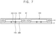
- FIGS. 4 to 7 are cross-sectional views illustrating a method of manufacturing a semiconductor package in accordance with example embodiments.
- FIGS. 5 and 6 are cross-sectional views illustrating a process of encapsulating a semiconductor chip using a molding apparatus.
- a plurality of semiconductor chips 200 may be arranged on a substrate 20 .
- the semiconductor chips 200 may be mounted on the substrate 20 by a flip chip bonding process.
- the semiconductor chips 200 may be mounted on the substrate 20 using the conductive bumps 220 as a connecting medium and may be arranged in a matrix form.
- the conductive bumps 220 may be disposed on connection pads, e.g., substrate pads 110 of the substrate 20 , and the conductive bumps 220 may be respectively attached on the substrate pads 110 by, e.g., a reflowing process, such that the semiconductor chips 200 may each be mounted on the substrate 20 .
- the conductive bump 220 may include the lower and upper bumps stacked on each other.
- the lower bump may include a first conductive material with a first ductility
- the upper bump may include a second conductive material with a second ductility different (for example, greater) than the first ductility.
- the first conductive material may include copper (Cu), nickel (Ni) or etc.
- the second conductive material may include tin (Sn), tin/silver (Sn/Ag), tin/copper (Sn/Cu), tin/indium (Sn/In) or etc., though the present disclosure is not necessarily limited thereto.
- the substrate 20 may be a printed circuit board (PCB) substrate.
- the substrate 20 may include a chip mounting region for mounting the plurality of semiconductor chips 200 .
- the plurality of semiconductor chips 200 may be disposed on the chip mounting region.
- a molding material 40 may be formed on an upper surface of the substrate 20 to cover at least a portion of the semiconductor chips 200 and a mechanical reinforcing pattern 400 may be formed in the molding material 40 .
- a molding process may be performed using a molding apparatus 30 .
- the reinforcing pattern 400 may be positioned around the semiconductor chip 200 in the cavity 35 during a state in which the lower and upper molds 32 and 34 are clamped together.
- a molding material 40 may be injected into the cavity 35 and may be cured.
- the molding material 40 may include an epoxy mold compound (EMC).
- ejector pins 36 may be installed in at least one of the upper mold 34 and the lower mold 32 to dispose the mechanical reinforcing pattern 400 at a desired position within the cavity 35 .
- the ejector pins 36 may be moved to protrude from a lower surface of the upper mold 34 to support or separate the mechanical reinforcing pattern 400 in the cavity 35 .
- the substrate 20 may be loaded on the lower mold 32 of the molding apparatus 30 , and the mechanical reinforcing pattern 400 may be attached to and supported by the protruding ejector pins 36 and by an adhesive tape.
- the mechanical reinforcing pattern 400 may be positioned around the semiconductor chip 200 in the cavity 35 .
- the adhesive tape may include a polymer tape serving as a temporary adhesive. When the molding material 40 is injected and cured, the adhesive tape may lose adhesion, and at this time, the ejector pins 36 may be returned to the inside of the upper mold 34 .
- the ejector pins 36 may support the mechanical reinforcing pattern 400 by vacuum adsorption.
- the vacuum may be removed from the ejector pins 36 , and at this time, the ejector pins 36 may be returned to the inside of the upper mold 34 .
- the substrate 20 may be individually sawed, thereby manufacturing a plurality of flip chip packages.
- FIGS. 8 to 10 are plan views illustrating a reinforcing member in accordance with example embodiments.
- a reinforcing pattern may include a pair of support patterns 402 and 404 that are formed in both sides of a semiconductor chip 200 respectively.
- a first support pattern 402 may extend in a first direction (Y direction) along a first side surface S 1 of a molding member 300 .
- a second support pattern 404 may extend in the first direction (Y direction) along a second side surface S 2 of the molding member 300 opposite to the first side surface S 1 .
- the first support pattern 402 may be spaced apart from the first side S 1 of the first semiconductor chip 200 .
- the second support pattern 404 may be spaced apart from the second side S 2 of the semiconductor chip 200 .
- a reinforcing pattern may include a plurality of support patterns 403 a , 403 b , 403 c , 403 d that may be formed around edges of a semiconductor chip 200 .
- a first support pattern 403 a may be formed around a first edge of the semiconductor chip 200
- a second support pattern 403 b may be formed around a second edge of the semiconductor chip 200
- a third support pattern 403 c may be formed around a third edge of the semiconductor chip 200
- a fourth support pattern 403 c may be formed around a fourth edge of the semiconductor chip 200 .
- a reinforcing pattern may include a plurality of support patterns 402 , 404 , 406 , 408 that are provided around a semiconductor chip 200 and that may be spaced apart from each other.
- a first support pattern 402 may extend along a first side surface S 1 of a molding member 300 .
- a second support pattern 404 may extend along a second side surface S 2 of the molding member 300 opposite to the first side surface S 2 .
- a third support pattern 406 may extend along a third side surface S 3 of the molding member 300 adjacent to the first side surface.
- a fourth support pattern 408 may extend along a fourth side surface S 4 of the molding member 300 opposite to the third side surface.
- FIG. 11 is a plan view illustrating a semiconductor package in accordance with example embodiments.
- FIG. 12 is a cross-sectional view taken along the line C-C′ in FIG. 11 .
- the semiconductor package may be substantially the same as or similar to the semiconductor package described with reference to FIGS. 1 to 3 except for a mounting manner of a semiconductor chip.
- same reference numerals will be used to refer to the same or like elements and any further repetitive explanation concerning the above elements will be omitted.
- a semiconductor chip 200 of a semiconductor package 11 may be mounted on a package substrate 100 in a wire bonding manner.
- the semiconductor chip 200 may be adhered on the package substrate 100 by an adhesive member 232 .
- Chip pads 210 may be formed or disposed on a first surface of the semiconductor chip 200 .
- the semiconductor chip 200 may be adhered on the package substrate 100 such that a second surface opposite to the first surface faces the package substrate 100 .
- the adhesive member 232 may include epoxy, polyimide, etc.
- the adhesive member 232 may include an adhesive film such as DAF (direct adhesive film).
- the chip pads 210 of the semiconductor chip 200 may be electrically connected to substrate pads 110 of the package substrate 100 .
- a bonding wire 222 may include a conductive material, such as gold or aluminum.
- a molding member 300 may be provided on the package substrate 100 to cover at least a portion of the semiconductor chip 200 and the bonding wires 222 .
- a reinforcing pattern 400 may be provided within the molding member 300 to extend around the semiconductor chip 200 .
- a portion of the reinforcing pattern 400 may extend in one direction (Y direction) along the bonding wires 222 .
- the reinforcing pattern 400 may be arranged outside the bonding wires 222 .
- FIGS. 13 and 14 are cross-sectional views illustrating a method of manufacturing a semiconductor package in accordance with example embodiments.
- a plurality of semiconductor chips 200 may be arranged on a substrate 20 .
- the semiconductor chips 200 may be mounted on the substrate 20 by a wire bonding process.
- the semiconductor chips 200 may be adhered on an upper surface of the substrate 20 using adhesive members 232 .
- the adhesive member may include an adhesive film such as DAF (direct adhesive film).
- a wire bonding process may be performed to electrically connect the semiconductor chip 200 to the substrate 20 .
- Chip pads 210 of the semiconductor chip 200 may be electrically connected to substrate pads 110 on the upper surface of the substrate 20 by the wire bonding process.
- the chip pads 210 of the semiconductor chip 200 may be electrically connected to substrate pads 110 by bonding wires 222 .
- a molding material 40 may be formed on the upper surface of the substrate 20 to cover at least a portion of the semiconductor chips 200 and a mechanical reinforcing pattern 400 may be formed within the molding material 40 .
- Processes the same as or similar to the processes described with reference to FIGS. 5 and 6 may be performed to form the molding material 40 on the substrate 20 to cover at least a portion of the semiconductor chips 200 and the mechanical reinforcing pattern 400 within the molding material 40 to extend around the semiconductor chip 200 .
- the substrate 20 may be individually sawed, thereby manufacturing a plurality of semiconductor chip packages.
- the semiconductor package may include semiconductor devices such as logic devices or memory devices.
- the semiconductor package may include logic devices such as central processing units (CPUs), main processing units (MPUs), or application processors (APs), or the like, and volatile memory devices such as DRAM devices, HBM devices, or non-volatile memory devices such as flash memory devices, PRAM devices, MRAM devices, ReRAM devices, or the like.
- logic devices such as central processing units (CPUs), main processing units (MPUs), or application processors (APs), or the like
- volatile memory devices such as DRAM devices, HBM devices, or non-volatile memory devices such as flash memory devices, PRAM devices, MRAM devices, ReRAM devices, or the like.
Landscapes
- Engineering & Computer Science (AREA)
- Physics & Mathematics (AREA)
- Condensed Matter Physics & Semiconductors (AREA)
- General Physics & Mathematics (AREA)
- Computer Hardware Design (AREA)
- Microelectronics & Electronic Packaging (AREA)
- Power Engineering (AREA)
- Manufacturing & Machinery (AREA)
- Chemical & Material Sciences (AREA)
- Dispersion Chemistry (AREA)
- Structures Or Materials For Encapsulating Or Coating Semiconductor Devices Or Solid State Devices (AREA)
- Encapsulation Of And Coatings For Semiconductor Or Solid State Devices (AREA)
Abstract
A semiconductor package includes a package substrate, at least one semiconductor chip mounted on the package substrate, a molding member on the package substrate to cover at least a portion of the semiconductor chip, and a mechanical reinforcing member provided around the semiconductor chip within the molding member and extending in at least one direction.
Description
This application is a continuation application of U.S. application Ser. No. 17/212,364, filed on Mar. 25, 2021, which claims priority under 35 U.S.C. § 119 to Korean Patent Application No. 10-2020-0077095, filed on Jun. 24, 2020 in the Korean Intellectual Property Office (KIPO), the contents of which are herein incorporated by reference in their entirety.
Example embodiments relate to a semiconductors, and more particularly, to a semiconductor package and method of manufacturing a semiconductor package.
According to the trend of miniaturization of various electronic products using semiconductor devices, semiconductor packages are becoming smaller, thinner, and lighter. Thus, cracks may easily occur in the semiconductor package due to external impact. In particular, in the automotive field, package cracks due to mechanical damage may cause personal injury. Additionally, thermal expansion and contraction and may case cracks in some semiconductor packages.
According to example embodiments, a semiconductor package includes, a package substrate, at least one semiconductor chip mounted on the package substrate, a molding member on the package substrate to cover at least a portion of the semiconductor chip, and a mechanical reinforcing member provided around the semiconductor chip within the molding member and extending in at least one direction.
According to example embodiments, a semiconductor package includes, a package substrate having an upper surface and a lower surface opposite to each other, at least one semiconductor chip mounted on the upper surface of the package substrate, a molding member on the upper surface of the package substrate to cover at least a portion of the semiconductor chip, and a reinforcing member provided in at least a portion of the molding member and extending around the semiconductor chip.
According to example embodiments, in a method of manufacturing a semiconductor package, a semiconductor chip is arranged on a substrate. The substrate is disposed in a cavity between a lower mold and an upper mold of a molding apparatus. A mechanical reinforcing pattern is positioned around the semiconductor chip within the cavity. A molding material is injected into the cavity and cured.
According to example embodiments, a semiconductor package may include a mechanical reinforcing pattern within a molding member which covers a semiconductor chip provided on a package substrate. The mechanical reinforcing pattern may extend in at least one direction around the semiconductor chip within the molding member. The mechanical reinforcing pattern may include a material different from the molding member to serve as a mechanical reinforcing member to improve mechanical properties of the semiconductor package. A material, physical properties, and a size of the reinforcing pattern may be selected to prevent cracks and improve mechanical properties of the semiconductor package.
Example embodiments will be more clearly understood from the following detailed description when considered in connection with the accompanying drawings.
Hereinafter, example embodiments will be described in detail with reference to the accompanying drawings.
Referring to FIGS. 1 to 3 , a semiconductor package 10 may include a package substrate 100, at least one semiconductor chip 200 arranged on an upper surface 102 of the package substrate 100, a molding member 300 on the upper surface 102 of the package substrate 100 to cover at least a portion of the semiconductor chip 200, and a reinforcing member extending in at least one direction within the molding member 300. The semiconductor package 10 may further include outer connection members 500 disposed on a lower surface 104 of the package substrate 100.
In example embodiments, the package substrate 100 may be a substrate having the upper surface 102 and the lower surface 104 opposite to each other. For example, the package substrate 100 may be a printed circuit board (PCB). The PCB may be a multilayered circuit board, and may include vias and various circuits therein.
The package substrate 100 may have a rectangular shape. The package substrate 100 may have a chip mounting region and a peripheral region surrounding the chip mounting region. The semiconductor chip 200 may be disposed on the upper surface 102 of the package substrate 100. The semiconductor chip 200 may be mounted on the chip mounting region and have a footprint (e.g., an area from a top down view) matching or similar to the area of the chip mounting region.
A plurality of substrate pads 110 may be provided on the upper surface 102 of the package substrate 100. The substrate pads 110 may be arranged within the chip mounting region. At least a portion of the substrate pad 110 may be used as a connection pad for electrical connection with the semiconductor chip 200.
A first insulation layer may be provided on the upper surface 102 of the package substrate 100. The first insulation layer may cover the entire upper surface 102 of the package substrate except for at least a portion of the substrate pad 110. The first insulation layer may expose a portion of the substrate pad 110. In some examples, the first insulation layer may expose one or more substrate pads 110 to a portion of the substrate 100. In some examples, the first insulation layer may include solder resist, silicon oxide, silicon nitride, silicon oxynitride, etc.
In example embodiments, the semiconductor chip 200 may have a plurality of chip pads 210 on a first surface, that is, active surface thereof. The semiconductor chip 200 may be mounted on the package substrate 100 such that the first surface on which the chip pads 210 are formed faces the package substrate 100.
In some embodiments, semiconductor chip 200 may be mounted on the package substrate 100 in a flip chip bonding manner. The semiconductor chip 200 may be mounted on the package substrate 100 via conductive bumps 220. The conductive bump 220 may be interposed between the substrate pad 110 of the package substrate 100 and the chip pad 210 of the semiconductor chip 200 to electrically connect the semiconductor chip 200 and the package substrate 100.
A plurality of the conductive bumps 220 may be disposed on the substrate pads 110 respectively. The conductive bumps 220 may be attached on the chip pads 210 of the semiconductor chip 200 respectively. The semiconductor chip 200 may be stacked on the package substrate 100 by disposing the conductive bumps 220 to substrate pads 110, thereby forming an electrical connection to the package substrate 100.
For example, the conductive bump 220 may include a micro bump, a solder bump, a solder ball, etc. The conductive bump 20 may include a metal such as copper (Cu), nickel (Ni), tin (Sn), tin/silver (Sn/Ag), tin/copper (Sn/Cu), tin/indium (Sn/In) or etc.
An underfill member 230 may be provided between the semiconductor chip 200 and the package substrate 100. The underfill member 230 may fill a space between the upper surface 102 of the package substrate 100 and the semiconductor chip 200. The underfill member 230 may include epoxy molding compound (EMC). The underfill member may be formed together with the molding member 300 by a molded underfill (MUF) process. Alternatively, the underfill member may be formed by a process separate from a process of forming the molding member 300.
Although only some substrate pads and chip pads are illustrated in the figures, the number and arrangements of the substrate pads and the chip pads and molding member represent example embodiments of the present disclosure, and the present disclosure is not necessarily limited thereto. Further, although one semiconductor chip is illustrated in the figures, the present disclosure is not necessarily limited thereto, and a plurality of semiconductor chips may be stacked on the package substrate.
In example embodiments, the molding member 300 may be provided on the package substrate 100 to cover at least a portion of the semiconductor chip 200 thereby protecting the semiconductor chip 200 from external impacts. For example, the molding member may include epoxy mold compound (EMC). The molding member 300 may be formed by a molding process, a screen printing process, a lamination process, etc.
The molding member 300 may have a rectangular shape corresponding to the shape of the package substrate 100. The molding member 300 may have a first side surface S1 and a second side surface S2 opposite to each other and extending in a direction parallel with a first direction (Y direction) which is perpendicular to the upper surface 102 of the package substrate 100. The molding member may have a third side surface S3 and a fourth side surface S4 opposite to each other and extending in a direction parallel with a second direction (X direction) which is perpendicular to the first direction.
A length in the first direction (Y direction) of the molding member 300 may be substantially the same as a length in the first direction (Y direction) of the package substrate 100 and may define a longitudinal direction length (L), and a length in the second direction (X direction) of the molding member 300 may be substantially the same as a length in the second direction (X direction) of the package substrate 100 and may define a traverse direction length (W).
In example embodiments, the reinforcing pattern 400 may be provided in at least a portion of the molding member 300 to extend around the semiconductor chip 200. The molding member 300 may cover at least a portion of the reinforcing member 400. Accordingly, an outer surface of the reinforcing member 400 might not be exposed to the outside.
As illustrated in FIG. 1 , the reinforcing pattern 400 may have a ring shape extending around the semiconductor chip 200. The reinforcing pattern 400 may be spaced apart from the upper surface 102 of the package substrate 100. The reinforcing pattern 400 may be arranged over a peripheral region of the package substrate 100. The reinforcing pattern 400 may be spaced apart from an outer surface of the semiconductor chip 200.
The reinforcing pattern 400 may include a material different from the molding member 300 to serve as a mechanical reinforcing member to strengthen the semiconductor package 10. For example, the reinforcing pattern 400 may include a metal such as iron (Fe), aluminum (Al), copper (Cu), etc., or a plastic material.
In example embodiments, the molding member 300 may have a first tensile strength, and the reinforcing pattern 400 may have a second tensile strength greater than the first tensile strength. Since the reinforcing pattern 400 has a relatively high rigidity, it may be possible to prevent cracks from occurring in the semiconductor package 10.
The molding member 300 may have a first coefficient of thermal expansion, the reinforcing pattern 400 may have a second coefficient of thermal expansion different from the first coefficient of thermal expansion, and the package substrate 100 may have a third coefficient of thermal expansion different from the second coefficient of thermal expansion. The second coefficient of thermal expansion of the reinforcing pattern 400 may be determined to prevent warpage of the semiconductor package. For example, the second coefficient of thermal expansion may be greater than the first coefficient of thermal expansion. Since the reinforcing pattern 400 has a thermal expansion coefficient different from those of the molding member 300 and the package substrate 100, they semiconductor package 10 may be less likely to warp.
The material and physical properties (e.g., strength, coefficient of thermal expansion, elastic modulus, glass transition temperature, etc.) and size (e.g., length, thickness, width, etc.) of the reinforcing pattern 400 may be selected in order to prevent cracks in the semiconductor package 10 and strengthen the mechanical integrity of the package.
In example embodiments, external connection pads 120 may be provided on the lower surface 104 of the package substrate 100, and an electrical signal may be supplied to and from the semiconductor chip 200 through the external connection pads 120. A second insulation layer may be provided on the lower surface 104 of the package substrate 100. The external connection pads 120 may be exposed by the second insulation layer. For example, the second insulation layer may expose external connection pads 120 to external connection members 500. The second insulation layer may include a silicon oxide layer, a silicon nitride layer, a silicon oxynitride layer, etc. External connection members 500 may respectively be disposed on the external connection pads 120 of the package substrate 100 to be electrically connected to an external device. The external connection members 500 may be, for example, solder balls. The semiconductor package 10 may be mounted on a module substrate using the solder balls as a connecting medium to form part of a memory module.
As mentioned above, the semiconductor package 10 may include the mechanical reinforcing pattern 400 within the molding member 300 that covers the semiconductor chip 200 provided on the package substrate 100. The mechanical reinforcing pattern 400 may extend in at least one direction around the semiconductor chip 200 within the molding member 300. The reinforcing pattern 400 may include a material different from the molding member 300 to serve as a mechanical reinforcing member to strengthen the semiconductor package 10. The material, physical properties, and size of the reinforcing pattern may be selected to prevent cracks and increase of the structural integrity of the semiconductor package.
Thus, since the reinforcing pattern 400 has a relatively high rigidity, it may be possible to prevent cracks from occurring in the semiconductor package 10. Further, since the reinforcing pattern 400 has a thermal expansion coefficient different from those of the molding member 300 and the package substrate 100, the semiconductor package 10 may be less likely to warp when exposed to a temperature change.
Hereinafter, a method of manufacturing the semiconductor package in FIG. 1 will be described.
Referring to FIG. 4 , a plurality of semiconductor chips 200 may be arranged on a substrate 20.
In example embodiments, the semiconductor chips 200 may be mounted on the substrate 20 by a flip chip bonding process.
In particular, after forming conductive bumps 220 on chip pads 210 on a first surface of each semiconductor chip 200, the semiconductor chips 200 may be mounted on the substrate 20 using the conductive bumps 220 as a connecting medium and may be arranged in a matrix form. The conductive bumps 220 may be disposed on connection pads, e.g., substrate pads 110 of the substrate 20, and the conductive bumps 220 may be respectively attached on the substrate pads 110 by, e.g., a reflowing process, such that the semiconductor chips 200 may each be mounted on the substrate 20.
For example, after forming a seed layer on each chip pad 210 of each of the semiconductor chips 200, a plating process may be performed on the seed layer to sequentially form a lower bump portion and an upper bump portion on the seed layer. Accordingly, the conductive bump 220 may include the lower and upper bumps stacked on each other. The lower bump may include a first conductive material with a first ductility, and the upper bump may include a second conductive material with a second ductility different (for example, greater) than the first ductility. The first conductive material may include copper (Cu), nickel (Ni) or etc., and the second conductive material may include tin (Sn), tin/silver (Sn/Ag), tin/copper (Sn/Cu), tin/indium (Sn/In) or etc., though the present disclosure is not necessarily limited thereto.
The substrate 20 may be a printed circuit board (PCB) substrate. The substrate 20 may include a chip mounting region for mounting the plurality of semiconductor chips 200. The plurality of semiconductor chips 200 may be disposed on the chip mounting region.
Referring to FIGS. 5 to 7 , a molding material 40 may be formed on an upper surface of the substrate 20 to cover at least a portion of the semiconductor chips 200 and a mechanical reinforcing pattern 400 may be formed in the molding material 40.
As illustrated in FIGS. 5 and 6 , a molding process may be performed using a molding apparatus 30. After disposing the substrate 20 in a cavity 35 between a lower mold 32 and an upper mold 34 of the molding apparatus 30, the reinforcing pattern 400 may be positioned around the semiconductor chip 200 in the cavity 35 during a state in which the lower and upper molds 32 and 34 are clamped together. Then, a molding material 40 may be injected into the cavity 35 and may be cured. For example, the molding material 40 may include an epoxy mold compound (EMC).
In particular, ejector pins 36 may be installed in at least one of the upper mold 34 and the lower mold 32 to dispose the mechanical reinforcing pattern 400 at a desired position within the cavity 35. The ejector pins 36 may be moved to protrude from a lower surface of the upper mold 34 to support or separate the mechanical reinforcing pattern 400 in the cavity 35.
The substrate 20 may be loaded on the lower mold 32 of the molding apparatus 30, and the mechanical reinforcing pattern 400 may be attached to and supported by the protruding ejector pins 36 and by an adhesive tape. When the lower mold 32 and the upper mold 34 are clamped with each other, the mechanical reinforcing pattern 400 may be positioned around the semiconductor chip 200 in the cavity 35. The adhesive tape may include a polymer tape serving as a temporary adhesive. When the molding material 40 is injected and cured, the adhesive tape may lose adhesion, and at this time, the ejector pins 36 may be returned to the inside of the upper mold 34.
Alternatively, the ejector pins 36 may support the mechanical reinforcing pattern 400 by vacuum adsorption. When the molding material 40 is injected and cured, the vacuum may be removed from the ejector pins 36, and at this time, the ejector pins 36 may be returned to the inside of the upper mold 34.
Then, after curing the molding material, the substrate 20 may be individually sawed, thereby manufacturing a plurality of flip chip packages.
Referring to FIG. 8 , a reinforcing pattern may include a pair of support patterns 402 and 404 that are formed in both sides of a semiconductor chip 200 respectively. A first support pattern 402 may extend in a first direction (Y direction) along a first side surface S1 of a molding member 300. A second support pattern 404 may extend in the first direction (Y direction) along a second side surface S2 of the molding member 300 opposite to the first side surface S1. The first support pattern 402 may be spaced apart from the first side S1 of the first semiconductor chip 200. The second support pattern 404 may be spaced apart from the second side S2 of the semiconductor chip 200.
Referring to FIG. 9 , a reinforcing pattern may include a plurality of support patterns 403 a, 403 b, 403 c, 403 d that may be formed around edges of a semiconductor chip 200. A first support pattern 403 a may be formed around a first edge of the semiconductor chip 200, a second support pattern 403 b may be formed around a second edge of the semiconductor chip 200, a third support pattern 403 c may be formed around a third edge of the semiconductor chip 200 and a fourth support pattern 403 c may be formed around a fourth edge of the semiconductor chip 200.
Referring to FIG. 10 , a reinforcing pattern may include a plurality of support patterns 402, 404, 406, 408 that are provided around a semiconductor chip 200 and that may be spaced apart from each other. A first support pattern 402 may extend along a first side surface S1 of a molding member 300. A second support pattern 404 may extend along a second side surface S2 of the molding member 300 opposite to the first side surface S2. A third support pattern 406 may extend along a third side surface S3 of the molding member 300 adjacent to the first side surface. A fourth support pattern 408 may extend along a fourth side surface S4 of the molding member 300 opposite to the third side surface.
Referring to FIGS. 11 and 12 , a semiconductor chip 200 of a semiconductor package 11 may be mounted on a package substrate 100 in a wire bonding manner.
In example embodiments, the semiconductor chip 200 may be adhered on the package substrate 100 by an adhesive member 232. Chip pads 210 may be formed or disposed on a first surface of the semiconductor chip 200. The semiconductor chip 200 may be adhered on the package substrate 100 such that a second surface opposite to the first surface faces the package substrate 100. The adhesive member 232 may include epoxy, polyimide, etc. The adhesive member 232 may include an adhesive film such as DAF (direct adhesive film).
The chip pads 210 of the semiconductor chip 200 may be electrically connected to substrate pads 110 of the package substrate 100. A bonding wire 222 may include a conductive material, such as gold or aluminum.
In example embodiments, a molding member 300 may be provided on the package substrate 100 to cover at least a portion of the semiconductor chip 200 and the bonding wires 222. A reinforcing pattern 400 may be provided within the molding member 300 to extend around the semiconductor chip 200. A portion of the reinforcing pattern 400 may extend in one direction (Y direction) along the bonding wires 222. The reinforcing pattern 400 may be arranged outside the bonding wires 222.
Hereinafter, a method of manufacturing the semiconductor package in FIG. 11 will be described.
Referring to FIG. 13 , a plurality of semiconductor chips 200 may be arranged on a substrate 20.
In example embodiments, the semiconductor chips 200 may be mounted on the substrate 20 by a wire bonding process.
For example, the semiconductor chips 200 may be adhered on an upper surface of the substrate 20 using adhesive members 232. For example, the adhesive member may include an adhesive film such as DAF (direct adhesive film).
A wire bonding process may be performed to electrically connect the semiconductor chip 200 to the substrate 20. Chip pads 210 of the semiconductor chip 200 may be electrically connected to substrate pads 110 on the upper surface of the substrate 20 by the wire bonding process. For example, the chip pads 210 of the semiconductor chip 200 may be electrically connected to substrate pads 110 by bonding wires 222.
Referring to FIG. 14 , a molding material 40 may be formed on the upper surface of the substrate 20 to cover at least a portion of the semiconductor chips 200 and a mechanical reinforcing pattern 400 may be formed within the molding material 40.
Processes the same as or similar to the processes described with reference to FIGS. 5 and 6 may be performed to form the molding material 40 on the substrate 20 to cover at least a portion of the semiconductor chips 200 and the mechanical reinforcing pattern 400 within the molding material 40 to extend around the semiconductor chip 200.
Then, the substrate 20 may be individually sawed, thereby manufacturing a plurality of semiconductor chip packages.
The semiconductor package may include semiconductor devices such as logic devices or memory devices. The semiconductor package may include logic devices such as central processing units (CPUs), main processing units (MPUs), or application processors (APs), or the like, and volatile memory devices such as DRAM devices, HBM devices, or non-volatile memory devices such as flash memory devices, PRAM devices, MRAM devices, ReRAM devices, or the like.
The foregoing is illustrative of example embodiments and is not to be construed as limiting thereof. Although a few example embodiments have been described, those skilled in the art will readily appreciate that many modifications are possible in example embodiments without materially departing from the novel teachings and advantages of the present invention. Accordingly, all such modifications are intended to be included within the scope of example embodiments as disclosed.
Claims (20)
1. A method of manufacturing a semiconductor package, the method comprising:
disposing a semiconductor chip on a substrate;
disposing the substrate in a cavity between a lower mold and an upper mold of a molding apparatus;
after disposing the substrate in the cavity, a mechanical reinforcing pattern around the semiconductor chip within the cavity such that the mechanical reinforcing pattern is suspended at a predetermined height from the substrate;
injecting a molding material into the cavity; and
curing the molding material within the cavity.
2. The method of claim 1 , wherein positioning the mechanical reinforcing pattern within the cavity comprises:
supporting the mechanical reinforcing pattern in the cavity using ejector pins that are installed in at least one of the upper mold and the lower mold.
3. The method of claim 2 , wherein the mechanical reinforcing pattern is supported on the ejector pins by an adhesive tape.
4. The method of claim 2 , further comprising:
moving the ejector pins to protruding from a surface of the at least one of the upper mold and the lower mold; and
returning the ejector pins to an inside of the at least one of the upper mold and the lower mold when the molding material is cured.
5. The method of claim 1 , wherein the cured the molding material covers upper and lower sides of the mechanical reinforcing pattern.
6. The method of claim 1 , further comprising:
after curing the molding material, sawing the substrate into an individual semiconductor package.
7. The method of claim 1 , wherein arranging the semiconductor chip on the substrate is performed by a flip chip bonding process.
8. The method of claim 7 , wherein performing the flip chip bonding process includes mounting the semiconductor chip on the substrate using conductive bumps that are respectively attached on substrate pads of the substrate.
9. The method of claim 1 , wherein arranging the semiconductor chip on the substrate is performed by a wire bonding process.
10. The method of claim 1 , wherein performing the wire bonding process includes:
adhering the semiconductor chip on the substrate by an adhesive member; and
electrically connecting chip pads of the semiconductor chip to substrate pads of the substrate by bonding wires, respectively.
11. A method of manufacturing a semiconductor package, the method comprising:
disposing a semiconductor chip on a substrate;
after disposing the semiconductor chip on the substrate, positioning a mechanical reinforcing pattern around the semiconductor chip, the mechanical reinforcing pattern to be suspended at a predetermined height from the substrate; and
forming a molding material on the substrate to cover at least a portion of the semiconductor chip and upper and lower sides of the mechanical reinforcing pattern.
12. The method of claim 11 , wherein positioning the mechanical reinforcing pattern around the semiconductor chip comprises
disposing the substrate in a cavity between a lower mold and an upper mold of a molding apparatus; and
supporting the mechanical reinforcing pattern in the cavity using ejector pins that are installed in at least one of the upper mold and the lower mold.
13. The method of claim 12 , wherein the mechanical reinforcing pattern is supported on the ejector pins by an adhesive tape.
14. The method of claim 12 , further comprising:
moving the ejector pins to protruding from a surface of the at least one of the upper mold and the lower mold; and
returning the ejector pins to an inside of the at least one of the upper mold and the lower mold when the molding material is formed.
15. The method of claim 12 , wherein forming a molding material on the substrate comprises:
injecting the molding material into the cavity; and
curing the molding material within the cavity.
16. The method of claim 11 , further comprising:
after forming the molding material, sawing the substrate and the molding material into an individual semiconductor package.
17. The method of claim 11 , wherein the molding material has a first tensile strength, and wherein the mechanical reinforcing pattern has a second tensile strength greater than the first tensile strength.
18. The method of claim 11 , wherein the molding material has a first coefficient of thermal expansion, and wherein the mechanical reinforcing pattern has a second coefficient of thermal expansion different from the first coefficient of thermal expansion.
19. The method of claim 11 , wherein the mechanical reinforcing pattern has a ring shape extending around the semiconductor chip.
20. The method of claim 11 , wherein the mechanical reinforcing pattern includes a plurality of support patterns disposed around the semiconductor chip, and wherein the plurality of support patterns are spaced apart from each other.
Priority Applications (1)
| Application Number | Priority Date | Filing Date | Title |
|---|---|---|---|
| US18/174,576 US11894242B2 (en) | 2020-06-24 | 2023-02-24 | Semiconductor package and method of manufacturing semiconductor package |
Applications Claiming Priority (4)
| Application Number | Priority Date | Filing Date | Title |
|---|---|---|---|
| KR1020200077095A KR102796813B1 (en) | 2020-06-24 | 2020-06-24 | Semiconductor packages and method of manufacturing semiconductor packages |
| KR10-2020-0077095 | 2020-06-24 | ||
| US17/212,364 US11610786B2 (en) | 2020-06-24 | 2021-03-25 | Semiconductor package and method of manufacturing semiconductor package |
| US18/174,576 US11894242B2 (en) | 2020-06-24 | 2023-02-24 | Semiconductor package and method of manufacturing semiconductor package |
Related Parent Applications (1)
| Application Number | Title | Priority Date | Filing Date |
|---|---|---|---|
| US17/212,364 Continuation US11610786B2 (en) | 2020-06-24 | 2021-03-25 | Semiconductor package and method of manufacturing semiconductor package |
Publications (2)
| Publication Number | Publication Date |
|---|---|
| US20230223279A1 US20230223279A1 (en) | 2023-07-13 |
| US11894242B2 true US11894242B2 (en) | 2024-02-06 |
Family
ID=79031426
Family Applications (2)
| Application Number | Title | Priority Date | Filing Date |
|---|---|---|---|
| US17/212,364 Active 2041-06-08 US11610786B2 (en) | 2020-06-24 | 2021-03-25 | Semiconductor package and method of manufacturing semiconductor package |
| US18/174,576 Active US11894242B2 (en) | 2020-06-24 | 2023-02-24 | Semiconductor package and method of manufacturing semiconductor package |
Family Applications Before (1)
| Application Number | Title | Priority Date | Filing Date |
|---|---|---|---|
| US17/212,364 Active 2041-06-08 US11610786B2 (en) | 2020-06-24 | 2021-03-25 | Semiconductor package and method of manufacturing semiconductor package |
Country Status (2)
| Country | Link |
|---|---|
| US (2) | US11610786B2 (en) |
| KR (1) | KR102796813B1 (en) |
Families Citing this family (1)
| Publication number | Priority date | Publication date | Assignee | Title |
|---|---|---|---|---|
| US11532593B2 (en) * | 2020-09-30 | 2022-12-20 | Taiwan Semiconductor Manufacturing Co., Ltd. | Embedded stress absorber in package |
Citations (24)
| Publication number | Priority date | Publication date | Assignee | Title |
|---|---|---|---|---|
| US5793118A (en) | 1994-05-26 | 1998-08-11 | Nec Corporation | Semiconductor device capable of accomplishing a high moisture proof |
| US5953589A (en) | 1996-12-30 | 1999-09-14 | Anam Semiconductor Inc. | Ball grid array semiconductor package with solder balls fused on printed circuit board and method for fabricating the same |
| US5977626A (en) | 1998-08-12 | 1999-11-02 | Industrial Technology Research Institute | Thermally and electrically enhanced PBGA package |
| US6111306A (en) * | 1993-12-06 | 2000-08-29 | Fujitsu Limited | Semiconductor device and method of producing the same and semiconductor device unit and method of producing the same |
| US20020015607A1 (en) * | 2000-07-28 | 2002-02-07 | Hunt Imaging Llc | Ink cartridge |
| US20050257707A1 (en) * | 2004-05-18 | 2005-11-24 | Meca & Technology Machine, Inc. | Internally piped print cylinder and method for making same |
| US6982042B2 (en) | 2003-02-28 | 2006-01-03 | Hitachi Global Storage Technologies Netherlands, B.V. | Ion bombardment of electrical lapping guides to decrease noise during lapping process |
| US20060255471A1 (en) | 2003-01-29 | 2006-11-16 | Yong-Kwan Lee | Flip chip package having protective cap and method of fabricating the same |
| US7223673B2 (en) | 2004-07-15 | 2007-05-29 | Taiwan Semiconductor Manufacturing Company, Ltd. | Method of manufacturing semiconductor device with crack prevention ring |
| US7554182B2 (en) * | 2001-04-13 | 2009-06-30 | Yamaha Corporation | Semiconductor device and package, and method of manufacturer therefor |
| US20090289339A1 (en) | 2008-05-23 | 2009-11-26 | Advanced Semiconductor Engineering, Inc. | Semiconductor package and method for manufacturing the same |
| US7811063B2 (en) * | 2006-11-03 | 2010-10-12 | General Electric Company | Damping element for a wind turbine rotor blade |
| US7898093B1 (en) | 2006-11-02 | 2011-03-01 | Amkor Technology, Inc. | Exposed die overmolded flip chip package and fabrication method |
| US20120235308A1 (en) * | 2011-03-16 | 2012-09-20 | Renesas Electronics Corporation | Manufacturing method of semiconductor device, and semiconductor device |
| US20130119549A1 (en) * | 2011-11-16 | 2013-05-16 | Taiwan Semiconductor Manufacturing Company, Ltd. | Mold Chase Design for Package-on-Package Applications |
| US8742594B2 (en) | 2012-09-14 | 2014-06-03 | International Business Machines Corporation | Structure and method of making an offset-trench crackstop that forms an air gap adjacent to a passivated metal crackstop |
| US8779599B2 (en) | 2011-11-16 | 2014-07-15 | Taiwan Semiconductor Manufacturing Company, Ltd. | Packages including active dies and dummy dies and methods for forming the same |
| US8791562B2 (en) | 2010-07-21 | 2014-07-29 | Samsung Electronics Co., Ltd. | Stack package and semiconductor package including the same |
| US20140288220A1 (en) | 2013-03-25 | 2014-09-25 | E I Du Pont De Nemours And Company | Heat resistant polyamide compositions |
| US9536842B2 (en) | 2014-12-18 | 2017-01-03 | GlobalFoundries, Inc. | Structure with air gap crack stop |
| US20170194268A1 (en) | 2015-12-31 | 2017-07-06 | Taiwan Semiconductor Manufacturing Co., Ltd. | Lid Structure for a Semiconductor Device Package and Method for Forming the Same |
| US9768129B2 (en) | 2015-11-02 | 2017-09-19 | Samsung Electronics Co., Ltd. | Semiconductor device including three-dimensional crack detection structure |
| US20200020606A1 (en) | 2018-07-11 | 2020-01-16 | Samsung Electronics Co., Ltd. | Semiconductor package |
| US20200058551A1 (en) | 2018-08-20 | 2020-02-20 | Samsung Electronics Co., Ltd. | Methods of manufacturing semiconductor chip |
Family Cites Families (5)
| Publication number | Priority date | Publication date | Assignee | Title |
|---|---|---|---|---|
| TW200536827A (en) | 2004-05-04 | 2005-11-16 | Bristol Myers Squibb Co | Enzymatic ammonolysis process for the preparation of intermediates for DPP IV inhibitors |
| JP4171499B2 (en) * | 2006-04-10 | 2008-10-22 | 日立電線株式会社 | Electronic device substrate and manufacturing method thereof, and electronic device and manufacturing method thereof |
| KR20140057979A (en) * | 2012-11-05 | 2014-05-14 | 삼성전자주식회사 | Semiconductor package and method of manufacturing the semiconductor package |
| KR20180117238A (en) * | 2017-04-18 | 2018-10-29 | 삼성전자주식회사 | Semiconductor package and method for manufacturing the same |
| DE102018215796A1 (en) | 2018-09-18 | 2020-03-19 | Robert Bosch Gmbh | Position detection system and method for detecting a movement of a machine |
-
2020
- 2020-06-24 KR KR1020200077095A patent/KR102796813B1/en active Active
-
2021
- 2021-03-25 US US17/212,364 patent/US11610786B2/en active Active
-
2023
- 2023-02-24 US US18/174,576 patent/US11894242B2/en active Active
Patent Citations (24)
| Publication number | Priority date | Publication date | Assignee | Title |
|---|---|---|---|---|
| US6111306A (en) * | 1993-12-06 | 2000-08-29 | Fujitsu Limited | Semiconductor device and method of producing the same and semiconductor device unit and method of producing the same |
| US5793118A (en) | 1994-05-26 | 1998-08-11 | Nec Corporation | Semiconductor device capable of accomplishing a high moisture proof |
| US5953589A (en) | 1996-12-30 | 1999-09-14 | Anam Semiconductor Inc. | Ball grid array semiconductor package with solder balls fused on printed circuit board and method for fabricating the same |
| US5977626A (en) | 1998-08-12 | 1999-11-02 | Industrial Technology Research Institute | Thermally and electrically enhanced PBGA package |
| US20020015607A1 (en) * | 2000-07-28 | 2002-02-07 | Hunt Imaging Llc | Ink cartridge |
| US7554182B2 (en) * | 2001-04-13 | 2009-06-30 | Yamaha Corporation | Semiconductor device and package, and method of manufacturer therefor |
| US20060255471A1 (en) | 2003-01-29 | 2006-11-16 | Yong-Kwan Lee | Flip chip package having protective cap and method of fabricating the same |
| US6982042B2 (en) | 2003-02-28 | 2006-01-03 | Hitachi Global Storage Technologies Netherlands, B.V. | Ion bombardment of electrical lapping guides to decrease noise during lapping process |
| US20050257707A1 (en) * | 2004-05-18 | 2005-11-24 | Meca & Technology Machine, Inc. | Internally piped print cylinder and method for making same |
| US7223673B2 (en) | 2004-07-15 | 2007-05-29 | Taiwan Semiconductor Manufacturing Company, Ltd. | Method of manufacturing semiconductor device with crack prevention ring |
| US7898093B1 (en) | 2006-11-02 | 2011-03-01 | Amkor Technology, Inc. | Exposed die overmolded flip chip package and fabrication method |
| US7811063B2 (en) * | 2006-11-03 | 2010-10-12 | General Electric Company | Damping element for a wind turbine rotor blade |
| US20090289339A1 (en) | 2008-05-23 | 2009-11-26 | Advanced Semiconductor Engineering, Inc. | Semiconductor package and method for manufacturing the same |
| US8791562B2 (en) | 2010-07-21 | 2014-07-29 | Samsung Electronics Co., Ltd. | Stack package and semiconductor package including the same |
| US20120235308A1 (en) * | 2011-03-16 | 2012-09-20 | Renesas Electronics Corporation | Manufacturing method of semiconductor device, and semiconductor device |
| US20130119549A1 (en) * | 2011-11-16 | 2013-05-16 | Taiwan Semiconductor Manufacturing Company, Ltd. | Mold Chase Design for Package-on-Package Applications |
| US8779599B2 (en) | 2011-11-16 | 2014-07-15 | Taiwan Semiconductor Manufacturing Company, Ltd. | Packages including active dies and dummy dies and methods for forming the same |
| US8742594B2 (en) | 2012-09-14 | 2014-06-03 | International Business Machines Corporation | Structure and method of making an offset-trench crackstop that forms an air gap adjacent to a passivated metal crackstop |
| US20140288220A1 (en) | 2013-03-25 | 2014-09-25 | E I Du Pont De Nemours And Company | Heat resistant polyamide compositions |
| US9536842B2 (en) | 2014-12-18 | 2017-01-03 | GlobalFoundries, Inc. | Structure with air gap crack stop |
| US9768129B2 (en) | 2015-11-02 | 2017-09-19 | Samsung Electronics Co., Ltd. | Semiconductor device including three-dimensional crack detection structure |
| US20170194268A1 (en) | 2015-12-31 | 2017-07-06 | Taiwan Semiconductor Manufacturing Co., Ltd. | Lid Structure for a Semiconductor Device Package and Method for Forming the Same |
| US20200020606A1 (en) | 2018-07-11 | 2020-01-16 | Samsung Electronics Co., Ltd. | Semiconductor package |
| US20200058551A1 (en) | 2018-08-20 | 2020-02-20 | Samsung Electronics Co., Ltd. | Methods of manufacturing semiconductor chip |
Also Published As
| Publication number | Publication date |
|---|---|
| KR20210158587A (en) | 2021-12-31 |
| KR102796813B1 (en) | 2025-04-16 |
| US20210407821A1 (en) | 2021-12-30 |
| US20230223279A1 (en) | 2023-07-13 |
| US11610786B2 (en) | 2023-03-21 |
Similar Documents
| Publication | Publication Date | Title |
|---|---|---|
| US12406934B2 (en) | Semiconductor package | |
| KR100997793B1 (en) | Semiconductor package and manufacturing method thereof | |
| US8008771B2 (en) | Semiconductor chip package, electronic device including the semiconductor chip package and methods of fabricating the electronic device | |
| US7618849B2 (en) | Integrated circuit package with etched leadframe for package-on-package interconnects | |
| US8704349B2 (en) | Integrated circuit package system with exposed interconnects | |
| US20090014876A1 (en) | Wafer level stacked package having via contact in encapsulation portion and manufacturing method thereof | |
| US11705405B2 (en) | Packaged semiconductor devices having spacer chips with protective groove patterns therein | |
| US7049173B2 (en) | Method for fabricating semiconductor component with chip on board leadframe | |
| US20040171193A1 (en) | Semiconductor device and its manufacturing method | |
| US11894242B2 (en) | Semiconductor package and method of manufacturing semiconductor package | |
| US20250364467A1 (en) | Semiconductor package and method of manufacturing | |
| US20090129036A1 (en) | Semiconductor device and electronic device | |
| US20230395526A1 (en) | Semiconductor package and methods of manufacturing | |
| US20080073774A1 (en) | Chip package and chip package array | |
| KR20220078131A (en) | Hybrid semiconductor device and electronic device including the same | |
| US12308253B2 (en) | Molded product for semiconductor strip and method of manufacturing semiconductor package | |
| US20250079334A1 (en) | Reinforcement structures for multi-die semiconductor packages and methods of forming the same | |
| KR101266519B1 (en) | semiconductor package and its manufacturing method | |
| US12438134B2 (en) | Package substrate and semiconductor package including the same | |
| US20240429110A1 (en) | Semiconductor package and method of manufacturing the semiconductor package | |
| US20250364516A1 (en) | Semiconductor package | |
| US20250105152A1 (en) | Semiconductor package and method of manufacturing semiconductor package | |
| KR20260021128A (en) | Semiconductor package | |
| KR102002786B1 (en) | Semiconductor package and method for manufacturing the same | |
| KR20250033808A (en) | Semiconductor package |
Legal Events
| Date | Code | Title | Description |
|---|---|---|---|
| FEPP | Fee payment procedure |
Free format text: ENTITY STATUS SET TO UNDISCOUNTED (ORIGINAL EVENT CODE: BIG.); ENTITY STATUS OF PATENT OWNER: LARGE ENTITY |
|
| STPP | Information on status: patent application and granting procedure in general |
Free format text: NOTICE OF ALLOWANCE MAILED -- APPLICATION RECEIVED IN OFFICE OF PUBLICATIONS |
|
| STPP | Information on status: patent application and granting procedure in general |
Free format text: PUBLICATIONS -- ISSUE FEE PAYMENT VERIFIED |
|
| STCF | Information on status: patent grant |
Free format text: PATENTED CASE |