US11551866B2 - Multilayer ceramic capacitor and method of manufacturing the same - Google Patents
Multilayer ceramic capacitor and method of manufacturing the same Download PDFInfo
- Publication number
- US11551866B2 US11551866B2 US16/799,109 US202016799109A US11551866B2 US 11551866 B2 US11551866 B2 US 11551866B2 US 202016799109 A US202016799109 A US 202016799109A US 11551866 B2 US11551866 B2 US 11551866B2
- Authority
- US
- United States
- Prior art keywords
- side margin
- ceramic body
- thickness
- regions
- internal electrodes
- Prior art date
- Legal status (The legal status is an assumption and is not a legal conclusion. Google has not performed a legal analysis and makes no representation as to the accuracy of the status listed.)
- Active
Links
- 239000003985 ceramic capacitor Substances 0.000 title claims abstract description 63
- 238000004519 manufacturing process Methods 0.000 title claims description 14
- 239000000919 ceramic Substances 0.000 claims abstract description 200
- 239000011777 magnesium Substances 0.000 claims abstract description 139
- FYYHWMGAXLPEAU-UHFFFAOYSA-N Magnesium Chemical compound [Mg] FYYHWMGAXLPEAU-UHFFFAOYSA-N 0.000 claims abstract description 70
- 229910052749 magnesium Inorganic materials 0.000 claims abstract description 70
- 239000010936 titanium Substances 0.000 claims description 24
- 238000000034 method Methods 0.000 claims description 19
- 238000005245 sintering Methods 0.000 claims description 16
- RTAQQCXQSZGOHL-UHFFFAOYSA-N Titanium Chemical compound [Ti] RTAQQCXQSZGOHL-UHFFFAOYSA-N 0.000 claims description 12
- 229910052719 titanium Inorganic materials 0.000 claims description 12
- 238000005520 cutting process Methods 0.000 claims description 9
- 230000015556 catabolic process Effects 0.000 description 17
- 239000000203 mixture Substances 0.000 description 11
- 230000000052 comparative effect Effects 0.000 description 8
- 229910002113 barium titanate Inorganic materials 0.000 description 6
- 239000003990 capacitor Substances 0.000 description 5
- 239000000463 material Substances 0.000 description 5
- 229910010293 ceramic material Inorganic materials 0.000 description 4
- 230000007547 defect Effects 0.000 description 4
- 238000009826 distribution Methods 0.000 description 4
- 230000005684 electric field Effects 0.000 description 4
- 239000000843 powder Substances 0.000 description 4
- PXHVJJICTQNCMI-UHFFFAOYSA-N Nickel Chemical compound [Ni] PXHVJJICTQNCMI-UHFFFAOYSA-N 0.000 description 3
- KDLHZDBZIXYQEI-UHFFFAOYSA-N Palladium Chemical compound [Pd] KDLHZDBZIXYQEI-UHFFFAOYSA-N 0.000 description 3
- 239000000853 adhesive Substances 0.000 description 3
- 230000001070 adhesive effect Effects 0.000 description 3
- JRPBQTZRNDNNOP-UHFFFAOYSA-N barium titanate Chemical compound [Ba+2].[Ba+2].[O-][Ti]([O-])([O-])[O-] JRPBQTZRNDNNOP-UHFFFAOYSA-N 0.000 description 3
- 230000006866 deterioration Effects 0.000 description 3
- 238000009413 insulation Methods 0.000 description 3
- 230000008901 benefit Effects 0.000 description 2
- 238000001354 calcination Methods 0.000 description 2
- 239000010949 copper Substances 0.000 description 2
- 230000003247 decreasing effect Effects 0.000 description 2
- 238000009792 diffusion process Methods 0.000 description 2
- 239000013013 elastic material Substances 0.000 description 2
- 229910052751 metal Inorganic materials 0.000 description 2
- 239000002184 metal Substances 0.000 description 2
- 238000007639 printing Methods 0.000 description 2
- 238000004080 punching Methods 0.000 description 2
- 239000011800 void material Substances 0.000 description 2
- RYGMFSIKBFXOCR-UHFFFAOYSA-N Copper Chemical compound [Cu] RYGMFSIKBFXOCR-UHFFFAOYSA-N 0.000 description 1
- 239000000654 additive Substances 0.000 description 1
- 230000000996 additive effect Effects 0.000 description 1
- 239000000956 alloy Substances 0.000 description 1
- 229910045601 alloy Inorganic materials 0.000 description 1
- 239000011230 binding agent Substances 0.000 description 1
- 229910052802 copper Inorganic materials 0.000 description 1
- 239000002003 electrode paste Substances 0.000 description 1
- 238000005516 engineering process Methods 0.000 description 1
- 238000007646 gravure printing Methods 0.000 description 1
- 239000001257 hydrogen Substances 0.000 description 1
- 229910052739 hydrogen Inorganic materials 0.000 description 1
- 125000004435 hydrogen atom Chemical class [H]* 0.000 description 1
- 238000012986 modification Methods 0.000 description 1
- 230000004048 modification Effects 0.000 description 1
- 229910052759 nickel Inorganic materials 0.000 description 1
- 239000012299 nitrogen atmosphere Substances 0.000 description 1
- 239000003960 organic solvent Substances 0.000 description 1
- 229910052763 palladium Inorganic materials 0.000 description 1
- 230000003014 reinforcing effect Effects 0.000 description 1
- 238000007650 screen-printing Methods 0.000 description 1
- 239000002002 slurry Substances 0.000 description 1
- VEALVRVVWBQVSL-UHFFFAOYSA-N strontium titanate Chemical compound [Sr+2].[O-][Ti]([O-])=O VEALVRVVWBQVSL-UHFFFAOYSA-N 0.000 description 1
- 239000000126 substance Substances 0.000 description 1
Images


Classifications
-
- H—ELECTRICITY
- H01—ELECTRIC ELEMENTS
- H01G—CAPACITORS; CAPACITORS, RECTIFIERS, DETECTORS, SWITCHING DEVICES, LIGHT-SENSITIVE OR TEMPERATURE-SENSITIVE DEVICES OF THE ELECTROLYTIC TYPE
- H01G4/00—Fixed capacitors; Processes of their manufacture
- H01G4/002—Details
- H01G4/005—Electrodes
- H01G4/015—Special provisions for self-healing
-
- H—ELECTRICITY
- H01—ELECTRIC ELEMENTS
- H01G—CAPACITORS; CAPACITORS, RECTIFIERS, DETECTORS, SWITCHING DEVICES, LIGHT-SENSITIVE OR TEMPERATURE-SENSITIVE DEVICES OF THE ELECTROLYTIC TYPE
- H01G4/00—Fixed capacitors; Processes of their manufacture
- H01G4/002—Details
- H01G4/018—Dielectrics
- H01G4/06—Solid dielectrics
- H01G4/08—Inorganic dielectrics
- H01G4/12—Ceramic dielectrics
-
- H—ELECTRICITY
- H01—ELECTRIC ELEMENTS
- H01G—CAPACITORS; CAPACITORS, RECTIFIERS, DETECTORS, SWITCHING DEVICES, LIGHT-SENSITIVE OR TEMPERATURE-SENSITIVE DEVICES OF THE ELECTROLYTIC TYPE
- H01G4/00—Fixed capacitors; Processes of their manufacture
- H01G4/002—Details
- H01G4/005—Electrodes
- H01G4/008—Selection of materials
-
- H—ELECTRICITY
- H01—ELECTRIC ELEMENTS
- H01G—CAPACITORS; CAPACITORS, RECTIFIERS, DETECTORS, SWITCHING DEVICES, LIGHT-SENSITIVE OR TEMPERATURE-SENSITIVE DEVICES OF THE ELECTROLYTIC TYPE
- H01G4/00—Fixed capacitors; Processes of their manufacture
- H01G4/002—Details
- H01G4/018—Dielectrics
- H01G4/06—Solid dielectrics
- H01G4/08—Inorganic dielectrics
- H01G4/12—Ceramic dielectrics
- H01G4/1209—Ceramic dielectrics characterised by the ceramic dielectric material
- H01G4/1218—Ceramic dielectrics characterised by the ceramic dielectric material based on titanium oxides or titanates
- H01G4/1227—Ceramic dielectrics characterised by the ceramic dielectric material based on titanium oxides or titanates based on alkaline earth titanates
-
- H—ELECTRICITY
- H01—ELECTRIC ELEMENTS
- H01G—CAPACITORS; CAPACITORS, RECTIFIERS, DETECTORS, SWITCHING DEVICES, LIGHT-SENSITIVE OR TEMPERATURE-SENSITIVE DEVICES OF THE ELECTROLYTIC TYPE
- H01G4/00—Fixed capacitors; Processes of their manufacture
- H01G4/002—Details
- H01G4/224—Housing; Encapsulation
-
- H—ELECTRICITY
- H01—ELECTRIC ELEMENTS
- H01G—CAPACITORS; CAPACITORS, RECTIFIERS, DETECTORS, SWITCHING DEVICES, LIGHT-SENSITIVE OR TEMPERATURE-SENSITIVE DEVICES OF THE ELECTROLYTIC TYPE
- H01G4/00—Fixed capacitors; Processes of their manufacture
- H01G4/30—Stacked capacitors
-
- H—ELECTRICITY
- H01—ELECTRIC ELEMENTS
- H01G—CAPACITORS; CAPACITORS, RECTIFIERS, DETECTORS, SWITCHING DEVICES, LIGHT-SENSITIVE OR TEMPERATURE-SENSITIVE DEVICES OF THE ELECTROLYTIC TYPE
- H01G4/00—Fixed capacitors; Processes of their manufacture
- H01G4/002—Details
- H01G4/005—Electrodes
- H01G4/008—Selection of materials
- H01G4/0085—Fried electrodes
-
- H—ELECTRICITY
- H01—ELECTRIC ELEMENTS
- H01G—CAPACITORS; CAPACITORS, RECTIFIERS, DETECTORS, SWITCHING DEVICES, LIGHT-SENSITIVE OR TEMPERATURE-SENSITIVE DEVICES OF THE ELECTROLYTIC TYPE
- H01G4/00—Fixed capacitors; Processes of their manufacture
- H01G4/002—Details
- H01G4/228—Terminals
- H01G4/232—Terminals electrically connecting two or more layers of a stacked or rolled capacitor
-
- H—ELECTRICITY
- H01—ELECTRIC ELEMENTS
- H01G—CAPACITORS; CAPACITORS, RECTIFIERS, DETECTORS, SWITCHING DEVICES, LIGHT-SENSITIVE OR TEMPERATURE-SENSITIVE DEVICES OF THE ELECTROLYTIC TYPE
- H01G4/00—Fixed capacitors; Processes of their manufacture
- H01G4/002—Details
- H01G4/228—Terminals
- H01G4/248—Terminals the terminals embracing or surrounding the capacitive element, e.g. caps
Definitions
- the present disclosure relates to a multilayer ceramic capacitor having improved reliability by adjusting contents of magnesium (Mg) contained in a side margin portion and a cover portion, and a method of manufacturing the same.
- Mg magnesium
- electronic components using a ceramic material such as capacitors, inductors, piezoelectric elements, varistors, thermistors, or the like, include a ceramic body formed of a ceramic material, internal electrodes formed in the ceramic body, and external electrodes installed on a surface of the ceramic body to be connected to the internal electrodes.
- BDV breakdown voltage
- a sintering density of an external portion may be deteriorated due to the voids, such that moisture resistance reliability may be deteriorated.
- An aspect of the present disclosure may provide a multilayer ceramic capacitor having improved reliability by adjusting contents of magnesium (Mg) contained in a side margin portion and a cover portion, and a method of manufacturing the same.
- Mg magnesium
- a multilayer ceramic capacitor may include: a ceramic body including dielectric layers and having first and second surfaces opposing each other, third and fourth surfaces connecting the first and second surfaces, and fifth and sixth surfaces connected to the first to fourth surfaces and opposing each other; a plurality of internal electrodes disposed in the ceramic body, exposed to the first and second surfaces, and each having one end exposed to the third or fourth surface; and a first side margin portion and a second side margin portion disposed on end portions of the internal electrodes exposed to the first and second surfaces, respectively, wherein the ceramic body includes an active portion including the plurality of internal electrodes disposed to face each other with each of the dielectric layers interposed therebetween and forming capacitance, and cover portions disposed on upper and lower surfaces of the active portion, each of the first and second side margin portions is divided into a first region adjacent to an outer surface of the first and second side margin portions and a second region adjacent to the plurality of internal electrodes exposed to the first and second surfaces, each of the cover portions is divided into a first region
- a method of manufacturing a multilayer ceramic capacitor may include: preparing a first ceramic green sheet on which a plurality of first internal electrode patterns are disposed to have a predetermined interval therebetween and a second ceramic green sheet on which a plurality of second internal electrode patterns are disposed to have a predetermined interval therebetween, forming a ceramic green sheet laminate by stacking the first and second ceramic green sheets so that the plurality of first and second internal electrode patterns are alternated with each other, cutting the ceramic green sheet laminate to have side surfaces to which distal ends of the plurality of first and second internal electrode patterns are exposed in a width direction, forming a first side margin portion and a second side margin portion on the side surfaces of the ceramic green sheet laminate to which the distal ends of the plurality of first and second internal electrode patterns are exposed, and preparing a ceramic body including dielectric layers and first and second internal electrodes by sintering the cut ceramic green sheet laminate, wherein the ceramic body includes an active portion including the first and second internal electrodes disposed to face each
- a multilayer ceramic capacitor may include: a ceramic body including dielectric layers and having first and second surfaces opposing each other, third and fourth surfaces connecting the first and second surfaces, and fifth and sixth surfaces connected to the first to fourth surfaces and opposing each other; a plurality of internal electrodes disposed in the ceramic body, exposed to the first and second surfaces, and each having one end exposed to the third or fourth surface; and a first side margin portion and a second side margin portion disposed on end portions of the internal electrodes exposed to the first and second surfaces, respectively, wherein the ceramic body includes an active portion including the plurality of internal electrodes disposed to face each other with each of the dielectric layers interposed therebetween and forming capacitance, each of the first and second side margin portions is divided into a first region adjacent to an outer surface of the first and second side margin portions and a second region adjacent to the plurality of internal electrodes exposed to the first and second surfaces, and contents of magnesium (Mg) contained in the second regions of the first and second side margin portions are larger than
- FIG. 1 is a schematic perspective view illustrating a multilayer ceramic capacitor according to an exemplary embodiment in the present disclosure
- FIG. 2 is a perspective view illustrating an exterior of a ceramic body of FIG. 1 ;
- FIG. 3 is a perspective view of a ceramic green sheet laminate before sintering the ceramic body of FIG. 2 ;
- FIG. 4 is a side view illustrating of the ceramic body in a B direction of FIG. 2 ;
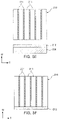
- FIGS. 5 A through 5 F are cross-sectional views and a perspective view schematically illustrating a method of manufacturing a multilayer ceramic capacitor according to another exemplary embodiment in the present disclosure.
- FIG. 6 is a graph illustrating results obtained by comparing breakdown voltages in Inventive Examples and Comparative Examples.
- FIG. 1 is a schematic perspective view illustrating a multilayer ceramic capacitor according to an exemplary embodiment in the present disclosure.
- FIG. 2 is a perspective view illustrating an exterior of a ceramic body of FIG. 1 .
- FIG. 3 is a perspective view of a ceramic green sheet laminate before sintering the ceramic body of FIG. 2 .
- FIG. 4 is a side view illustrating of the ceramic body in a B direction of FIG. 2 .
- a multilayer ceramic capacitor 100 may include a ceramic body 110 ; a plurality of internal electrodes 121 and 122 disposed in the ceramic body 110 ; and external electrodes 131 and 132 disposed on an outer surface of the ceramic body 110 .
- the ceramic body 110 may have first and second surfaces 1 and 2 opposing each other, third and fourth surfaces 3 and 4 connecting the first and second surfaces to each other, and fifth and sixth surfaces 5 and 6 corresponding to upper and lower surfaces, respectively.
- the first and second surfaces 1 and 2 may be defined as surfaces of the ceramic body 110 opposing each other in a width direction
- the third and fourth surfaces 3 and 4 may be defined as surfaces of the ceramic body 110 opposing each other in a length direction
- the fifth and sixth surfaces 5 and 6 may be defined as surfaces of the ceramic body 110 opposing each other in a thickness direction.
- a shape of the ceramic body 110 is not particularly limited, but may be a rectangular parallelepiped shape as illustrated.
- One end of each of the plurality of internal electrodes 121 and 122 disposed in the ceramic body 110 may be exposed to the third or fourth surface 3 or 4 of the ceramic body 110 .
- the internal electrodes 121 and 122 may be formed as a pair of first and second internal electrodes 121 and 122 having different polarities from each other.
- One end of the first internal electrode 121 may be exposed to the third surface 3 and one end of the second internal electrode 122 may be exposed to the fourth surface 4 .
- each of the first and second internal electrodes 121 and 122 may be spaced apart from the third or fourth surface 3 or 4 by a predetermined interval.
- the first and second external electrodes 131 and 132 may be formed on the third and fourth surfaces 3 and 4 of the ceramic body 110 to be electrically connected to the internal electrodes.
- the multilayer ceramic capacitor 100 may include the plurality of internal electrodes 121 and 122 disposed in the ceramic body 110 , exposed to the first and second surfaces 1 and 2 , and each having one end exposed to the third or fourth surface 3 or 4 .
- First and second side margin portions 112 and 113 may be disposed on end portions of the first and second internal electrodes 121 and 122 exposed to the first and second surfaces 1 and 2 , respectively.
- the plurality of internal electrodes 121 and 122 may be formed in the ceramic body 110 , a distal end of each of the plurality of internal electrodes 121 and 122 may be exposed to the first and second surfaces 1 and 2 , the surfaces of the ceramic body 110 in the width direction, and the first and second side margin portions 112 and 113 may be disposed on the exposed end portions, respectively.
- An average thickness d1 of the first and second side margin portions 112 and 113 may be 2 ⁇ m or more to 10 ⁇ m or less.
- the ceramic body 110 may include a laminate in which a plurality of dielectric layers 111 are stacked and the first and second side margin portions 112 and 113 disposed on both side surfaces of the laminate.
- the plurality of dielectric layers 111 may be in a sintered state and adjacent dielectric layers may be integrated with each other so that boundaries therebetween are not readily apparent.
- a length of the ceramic body 110 may correspond to a distance from the third surface 3 of the ceramic body 110 to the fourth surface 4 thereof.
- a length of the dielectric layer 111 may correspond to a distance from the third surface 3 of the ceramic body 110 to the fourth surface 4 thereof.
- the length of the ceramic body 110 may be 400 to 1400 ⁇ m, but is not limited thereto. In more detail, the length of the ceramic body 110 may be 400 to 800 ⁇ m or 600 to 1400 ⁇ m.
- the internal electrodes 121 and 122 may be formed on the dielectric layers 111 and be disposed in the ceramic body 110 with each of the dielectric layers 111 interposed therebetween by sintering.
- the first internal electrode 121 may be formed on the dielectric layer 111 .
- the first internal electrode 121 may not be entirely formed in a length direction of the dielectric layer 111 . That is, one end of the first internal electrode 121 may be formed to have a predetermined interval from the fourth surface 4 of the ceramic body 110 , and the other end of the first internal electrode 121 may be formed up to the third surface 3 of the ceramic body 110 to be exposed to the third surface 3 of the ceramic body 110 .
- the other end of the first internal electrode exposed to the third surface 3 of the ceramic body 110 may be connected to the first external electrode 131 .
- one end of the second internal electrode 122 may be formed to have a predetermined interval from the third surface 3 , and the other end of the second internal electrode 122 may be exposed to the fourth surface 4 to thereby be connected to the second external electrode 132 .
- the number of stacked internal electrode layers may be 400 or more, but is not necessarily limited thereto.
- the dielectric layer 111 may have the same width as that of the first internal electrode 121 . That is, the first internal electrode 121 may be entirely formed on the dielectric layer 111 in a width direction of the dielectric layer 111 .
- the width of the dielectric layer 111 and the width of the internal electrode may be 100 to 900 ⁇ m, but are not limited thereto. In more detail, the width of the dielectric layer 111 and the width of the internal electrode may be 100 to 500 ⁇ m or 100 to 900 ⁇ m.
- a thickness of the side margin portion may have an influence on electrical characteristics of the multilayer ceramic capacitor.
- the side margin portion may be formed to have a thickness of 10 ⁇ m or less, thereby improving characteristics of a miniaturized multilayer ceramic capacitor.
- the side margin portion may be formed to have a thickness of 10 ⁇ m or less, an area of an overlapping region between the internal electrodes forming capacitance may be secured as much as possible, such that a multilayer ceramic capacitor having high capacitance and a small size may be implemented.
- the ceramic body 110 as described above may include an active portion A as a portion contributing to forming capacitance of the capacitor and upper and lower cover portions 114 and 115 formed on upper and lower surfaces of the active portion A, respectively, as upper and lower margin portions.
- the active portion A may be formed by repeatedly stacking the plurality of first and second internal electrodes 121 and 122 with each of the dielectric layers 111 interposed therebetween.
- the upper and lower cover portions 114 and 115 may have the same material and configuration as those of the dielectric layer 111 except that internal electrodes are not included therein.
- the upper and lower cover portions 114 and 115 may contain a ceramic material, for example, a barium titanate (BaTiO 3 ) based ceramic material.
- Each of the upper and lower cover portions 114 and 115 may have a thickness of 20 ⁇ m, but is not necessarily limited thereto.
- the upper and lower cover portions 114 and 115 may be formed by stacking one or at least two dielectric layers on upper and lower surfaces, respectively, of the active portion A in the thickness direction, and generally serve to prevent the internal electrode from being damaged by physical or chemical stress.
- the internal electrode and the dielectric layer may be formed by being simultaneously cut, such that the width of the internal electrode may be equal to that of the dielectric layer. A more detailed description thereof will be described below.
- the dielectric layer may be formed to have the same width as that of the internal electrode, such that the distal ends of the internal electrodes 121 and 122 may be exposed to the first and second surfaces 1 and 2 of the ceramic body 110 in the width direction.
- the first and second side margin portions 112 and 113 may be formed on both side surfaces of the ceramic body 110 in the width direction, to which the distal ends of the internal electrodes 121 and 122 are exposed.
- the thickness of the first and second side margin portions 112 and 113 may be 10 ⁇ m or less. The thinner the thickness of the first and second side margin portions 112 and 113 , the wider the area of the overlapping region between the internal electrodes formed in the ceramic body 110 .
- the thickness of the first and second side margin portions 112 and 113 is not limited as long as short-circuit of the internal electrodes exposed to the side surface of the ceramic body 110 may be prevented.
- the thickness of the first and second side margin portions 112 and 113 may be 2 ⁇ m or more.
- the thickness of the first and second side margin portions is less than 2 ⁇ m, mechanical strength against external impact may be deteriorated, and when the thickness of the first and second side margin portions is more than 10 ⁇ m, the area of the overlapping region between the internal electrodes may relatively decrease, such that it may be difficult to secure high capacitance of the multilayer ceramic capacitor.
- the region of the margin portion needs to be significantly decreased in order to increase the overlapping region between the internal electrodes.
- the internal electrode may be formed on the entire dielectric layer in the width direction and the thickness of the side margin portion may be set to be 10 ⁇ m or less, such that the area of the overlapping region between the internal electrodes may become wide.
- the dielectric layer is highly stacked, thicknesses of the dielectric layer and the internal electrode may decrease. Therefore, the phenomenon that the internal electrodes are short-circuited may frequently occur.
- the internal electrode is formed only on a portion of the dielectric layer, an accelerated lifespan of insulating resistance or reliability may be deteriorated due to a step by the internal electrode.
- the present exemplary embodiment even though thin internal electrodes and thin dielectric layers are formed, since the internal electrode is entirely formed on the dielectric layer in the width direction, the area of the overlapping region between the internal electrodes may be increased, thereby increasing the capacitance of the multilayer ceramic capacitor.
- an accelerated lifespan of insulating resistance may be improved by decreasing the step by the internal electrode, such that a multilayer ceramic capacitor having excellent capacitance characteristics and reliability may be provided.
- the first and second side margin portions 112 and 113 may be divided into first regions 112 a and 113 a adjacent to outer surfaces of the side margin portions 112 and 113 and second regions 112 b and 113 b adjacent to the first and second internal electrodes 121 and 122 exposed to the first and second surfaces 1 and 2 of the ceramic body 110 , respectively.
- the content of magnesium (Mg) contained in the second regions 112 b and 113 b may be larger than the content of magnesium (Mg) contained in the first regions 112 a and 113 a.
- a breakdown voltage (BDV) may be increased and reliability may be improved by dividing the first and second side margin portions 112 and 113 disposed on the side surfaces of the ceramic body 110 into two regions having different compositions, respectively and adjusting the content of magnesium (Mg) contained in the second regions 112 b and 113 b to be larger than that in the first regions 112 a and 113 a.
- Mg magnesium
- a length of oxide layers of the distal ends of the internal electrodes exposed to the side surfaces of the ceramic body 110 in the width direction may be controlled by adjusting the content of magnesium (Mg) contained in the second regions 112 b and 113 b of the side margin portions adjacent to the internal electrodes 121 and 122 exposed to the first and second surfaces 1 and 2 of the ceramic body 110 , and thus, the breakdown voltage (BDV) may be increased and moisture resistance reliability may be improved.
- Mg magnesium
- a large number of voids may be formed in an interface between a ceramic body 110 and a side margin portion 112 and 113 at the time of forming the side margin portion, which may deteriorate reliability.
- BDV breakdown voltage
- a sintering density of an external portion may be deteriorated due to the voids, such that moisture resistance reliability may be deteriorated.
- an oxide layer may be formed in a void formed in an interface between the ceramic body 110 and the side margin portion 112 and 113 by adjusting the content of magnesium (Mg) contained in the second regions 112 b and 113 b at inner sides of the side margin portions 112 and 113 adjacent to the internal electrodes 121 and 122 exposed to the first and second surfaces 1 and 2 of the ceramic body 110 .
- Mg magnesium
- concentration of the electric field may be alleviated by securing insulation properties, such that the breakdown voltage (BDV) may increase and a short-circuit defect rate may decrease.
- BDV breakdown voltage
- a density of the first and second side margin portions 112 and 113 may be improved by dividing the first and second side margin portions 112 and 113 disposed on the side surfaces of the ceramic body 110 into two regions having different compositions, respectively and allowing the contents of magnesium (Mg) contained in the respective regions to be different from each other, such that moisture resistance may be improved.
- Mg magnesium
- a density of the first regions 112 a and 113 a of the first and second side margin portions 112 and 113 may be improved by adjusting the content of magnesium (Mg) contained in the second regions 112 b and 113 b of the side margin portions 112 and 113 to be larger than that in the first regions 112 a and 113 a , such that moisture resistance may be improved.
- Mg magnesium
- adhesive force with the first and second external electrodes 131 and 132 may be improved by allowing the first regions 112 a and 113 a of the first and second margin portions 112 and 113 adjacent to the outer surfaces of the side margin portions 112 and 113 to contain a small content of magnesium (Mg).
- Mg magnesium
- the content of magnesium (Mg) contained in the second regions 112 b and 113 b of the first and second side margin portions 112 and 113 may be adjusted to be larger than that in the first regions 112 a and 113 a by allowing a dielectric composition for forming the ceramic body 110 and a dielectric composition for forming the first and second side margin portions 112 and 113 to be different from each other in a process of manufacturing the multilayer ceramic capacitor 100 .
- the content of magnesium (Mg) contained in the second regions 112 b and 113 b may be adjusted to be larger than that in the first regions 112 a and 113 a.
- the electric field concentrated on distal end portions of the internal electrodes 121 and 122 may be alleviated, and reliability of the multilayer ceramic capacitor 100 may be improved by preventing insulation breakdown, which is one of main defects of a multilayer ceramic capacitor.
- the content of magnesium (Mg) in the second regions 112 b and 113 b of the first and second side margin portions 112 and 113 may be 10 moles or more to 30 moles or less based on titanium (Ti) contained in the first and second side margin portions.
- the breakdown voltage (BDV) may be increased, and moisture resistance reliability may be improved.
- the oxide layer is not sufficiently formed in the voids formed in the interface between the ceramic body 110 and the side margin portion 112 and 113 , such that the breakdown voltage (BDV) may decrease, and a short-circuit defect may be increased.
- the upper and lower cover portions 114 and 115 may be divided into first regions 114 a and 115 a adjacent to the outer surface of the ceramic body 110 and second regions 114 b and 115 b adjacent to internal electrodes disposed in outermost portions of the ceramic body 110 among the plurality of internal electrodes 121 and 122 , respectively, and the content of magnesium (Mg) contained in the second regions 114 b and 115 b may be larger than the content of magnesium (Mg) contained in the first regions 114 a and 115 a.
- a density of the upper and lower cover portions 114 and 115 may be improved, such that moisture resistance may be improved.
- the content of magnesium (Mg) contained in the second regions 114 b and 115 b of the upper and lower cover portions 114 and 115 may be larger than the content of magnesium (Mg) contained in the first regions 114 a and 115 a.
- the density of the upper and lower cover portions 114 and 115 may be improved by adjusting the content of magnesium (Mg) contained in the second regions 114 b and 115 b of the upper and lower cover portions 114 and 115 to be larger than the content of magnesium (Mg) contained in the first regions 114 a and 115 a , such that moisture resistance may be improved.
- adhesive force with the first and second external electrodes 131 and 132 may be improved by allowing the content of magnesium (Mg) contained in the first regions 114 a and 115 a of the upper and lower cover portions 114 and 115 adjacent to the outer surface of the ceramic body 110 to be relatively small.
- Mg magnesium
- the content of magnesium (Mg) contained in the second regions 114 b and 115 b of the upper and lower cover portions 114 and 115 may be 10 moles or more to 30 moles or less based on titanium (Ti) contained in the upper and lower cover portions 114 and 115 .
- Moisture resistance reliability may be improved by adjusting the content of magnesium (Mg) contained in the second regions 114 b and 115 b of the upper and lower cover portions 114 and 115 to be 10 moles or more to 30 moles or less based on titanium (Ti) contained in the upper and lower cover portions 114 and 115 .
- Mg magnesium
- Ti titanium
- the second regions 114 b and 115 b of the upper and lower cover portions 114 and 115 may further contain an additive for reinforcing adhesive force with the ceramic body 110 .
- the content of magnesium (Mg) contained in the second regions 114 b and 115 b of the upper and lower cover portions 114 and 115 may be adjusted to be larger than the content of magnesium (Mg) contained in the first regions 114 a and 115 a by allowing a dielectric composition for forming the ceramic body 110 and a dielectric composition for the cover portions to be different from each other in a manufacturing process of the multilayer ceramic capacitor.
- the content of magnesium (Mg) contained in the second regions 114 b and 115 b of the upper and lower cover portions 114 and 115 may be adjusted to be larger than the content of magnesium (Mg) contained in the first regions 114 a and 115 a.
- the multilayer ceramic capacitor according to the exemplary embodiment in the present disclosure may be a micro-sized multilayer ceramic capacitor in which a thickness of the dielectric layer 111 may be 0.4 ⁇ m or less, and a thickness of the first and second internal electrodes 121 and 122 is 0.4 ⁇ m or less.
- a reliability problem caused by voids generated in an interface between a ceramic body and a side margin portion is significantly important.
- the content of magnesium (Mg) in each region of the side margin portions needs to be adjusted.
- the breakdown voltage (BDV) may be increased, and moisture resistance reliability may be improved, even in a case of thin layers in which the dielectric layers 111 and the first and second internal electrodes 121 and 122 have a thickness of 4 ⁇ m or less.
- the term “thin layer” does not mean that the thicknesses of the dielectric layer 11 and the first and second internal electrodes 121 and 122 are 0.4 ⁇ m or less, but may be understood as a concept including dielectric layers and internal electrodes having a thin thickness as compared to a product according to the related art.
- a width of the first regions 112 a and 113 a of the first and second side margin portions 112 and 113 may be 12 ⁇ m or less and a width of the second regions 112 b and 113 b may be 3 ⁇ m or less, but are not necessarily limited thereto.
- a ratio of a thickness tc 2 of a region of the first or second side margin portion 112 and 113 coming into contact with a distal end of an internal electrode disposed in an outermost portion of the ceramic body 110 in the thickness direction to a thickness tc 1 of a region of the first or second side margin portion 112 and 113 coming into contact with a distal end of an internal electrode disposed in a central portion of the ceramic body 110 in the thickness direction among the plurality of internal electrodes 121 and 122 may be 1.0 or less.
- a lower limit value of the ratio of the thickness tc 2 of the region of the first or second side margin portion 112 and 113 coming into contact with the distal end of the internal electrode disposed in the outermost portion of the ceramic body 110 to the thickness tc 1 of the region of the first or second side margin portion 112 and 113 coming into contact with the distal end of the internal electrode disposed in the central portion of the ceramic body 110 is not particularly limited, but may be preferably 0.9 or more.
- the first 112 or second margin portion 113 is formed by attaching a ceramic green sheet to the side surface of the ceramic body 110 unlike the relate art, the thickness of the first 112 or second side margin portion 113 depending on a position is uniform.
- a thickness of a region of first or second side margin portion coming into contact with a distal end of an internal electrode disposed in a central portion of a ceramic body is formed to be thicker than that of other regions.
- a ratio of a thickness of a region of the first or second side margin portion coming into contact with a distal end of an internal electrode disposed in an outermost portion of the ceramic body to the thickness of the region of the first or second side margin portion coming into contact with the distal end of the internal electrode disposed in the central portion of the ceramic body 110 is less than 0.9, such that the deviation in thickness is large.
- the thickness of the side margin portions may be thin and the deviation in thickness may be small, such that a large size of the capacitance forming portion may be secured.
- a high-capacitance multilayer ceramic capacitor may be implemented.
- a ratio of a thickness tc 3 of a region of the first or second side margin portion 112 and 113 coming into contact with a corner of the ceramic body 110 to a thickness tc 1 of the region of the first or second side margin portion 112 and 113 coming into contact with the distal end of the internal electrode disposed in the central portion of the ceramic body 110 among the plurality of internal electrodes 121 and 122 may be 1.0 or less.
- a lower limit value of the ratio of the thickness tc 3 of the region of the first or second side margin portion 112 and 113 coming into contact with the corner of the ceramic body 110 to the thickness tc 1 of the region of the first or second side margin portion 112 and 113 coming into contact with the distal end of the internal electrode disposed in the central portion of the ceramic body 110 may be preferably 0.9 or more.
- the deviation in thickness of the side margin portion depending on the region may be small, such that a large size of the capacitance forming portion may be secured, thereby making it possible to implement a high capacitance multilayer ceramic capacitor.
- FIGS. 5 A through 5 F are cross-sectional views and a perspective view schematically illustrating a method of manufacturing a multilayer ceramic capacitor according to another exemplary embodiment in the present disclosure.
- a method of manufacturing a multilayer ceramic capacitor including: preparing a first ceramic green sheet on which a plurality of first internal electrode patterns are formed to have a predetermined interval therebetween and a second ceramic green sheet on which a plurality of second internal electrode patterns are formed to have a predetermined interval therebetween, forming a ceramic green sheet laminate by stacking the first and second green sheets so that the first and second internal electrode patterns are alternated with each other, cutting the ceramic green sheet laminate to have side surfaces to which distal ends of the first and second internal electrode patterns are exposed in a width direction, forming first and second side margin portions on the side surfaces of the ceramic green sheet laminate to which the distal ends of the first and second internal electrode patterns are exposed, and preparing a ceramic body including dielectric layers and first and second internal electrodes by sintering the cut laminate, wherein the ceramic body includes an active portion including the first and second internal electrodes disposed to face each other with each of the dielectric layers interposed therebetween and forming capacitance, and
- a plurality of stripe-type first internal electrode patterns 221 may be formed to have a predetermined interval therebetween on a ceramic green sheet 211 .
- the plurality of stripe-type first internal electrode patterns 221 may be formed in parallel with each other.
- the ceramic green sheet 211 may be formed of a ceramic paste containing a ceramic powder, an organic solvent, and an organic binder.
- the ceramic powder may be a material having high permittivity, and a barium titanate (BaTiO 3 )-based material, a lead complex perovskite-based material, strontium titanate (SrTiO 3 )-based material, or the like, may be used, but the ceramic powder is not limited thereto. Among them, barium titanate (BaTiO 3 ) powder may be preferable.
- the sintered ceramic green sheet 211 may become a dielectric layer 111 configuring a ceramic body 110 .
- the stripe-type first internal electrode pattern 221 may be formed of an internal electrode paste containing a conductive metal.
- the conductive metal may be nickel (Ni), copper (Cu), palladium (Pd), or an alloy thereof, but is not limited thereto.
- a method of forming the stripe-type first internal electrode pattern 221 on the ceramic green sheet 211 is not particularly limited.
- a printing method such as a screen printing method or a gravure printing method may be used.
- a plurality of stripe-type second internal electrode patterns 222 may be formed to have a predetermined interval therebetween on another ceramic green sheet 211 .
- the ceramic green sheet on which the first internal electrode pattern 221 is formed may be referred to as a first ceramic green sheet
- the ceramic green sheet on which the second internal electrode pattern 222 is formed may be referred to as a second ceramic green sheet.
- the first and second ceramic green sheets may be alternately stacked so that the stripe-type first internal electrode pattern 221 and the stripe-type second internal electrode pattern 222 are alternately stacked.
- the stripe-type first internal electrode pattern 221 may form a first internal electrode 121 and the stripe-type second internal electrode pattern 222 may form a second internal electrode 122 .
- a thickness td of the first and second ceramic green sheets may be 0.6 ⁇ m or less, and a thickness te of the first and second internal electrode patterns may be 0.5 ⁇ m or less.
- the multilayer ceramic capacitor according to the present disclosure may be a micro-sized high capacitance multilayer ceramic capacitor having thin layers in which a thickness of a dielectric layer is 0.4 ⁇ m or less, and a thickness of internal electrodes is 0.4 ⁇ m or less, the thickness td of the first and second ceramic green sheets may be 0.6 ⁇ m or less, and the thickness te of the first and second internal electrode patterns may be 0.5 ⁇ m or less.
- FIG. 5 C is a cross-sectional view illustrating a ceramic green sheet laminate 220 in which the first and second ceramic green sheets are stacked according to the exemplary embodiment in the present disclosure
- FIG. 5 D is a perspective view illustrating the ceramic green sheet laminate 220 in which the first and second ceramic green sheets are stacked.
- the first ceramic green sheet on which the plurality of stripe-type first internal electrode patterns 221 are printed in parallel and the second ceramic green sheet on which the plurality of stripe-type second internal electrode patterns 222 are printed in parallel may be alternately stacked.
- first and second ceramic green sheets may be stacked so that central portions of the stripe-type first internal electrode patterns 221 printed on the first ceramic green sheet and the intervals between the stripe-type second internal electrode patterns 222 printed on the second ceramic green sheet overlap each other.
- the ceramic green sheet laminate 220 may be cut so as to traverse the plurality of stripe-type first internal electrode patterns 221 and the plurality of stripe-type second internal electrode patterns 222 . That is, the ceramic green sheet laminate 220 may be cut into laminates 210 along cutting lines C 1 -C 1 and C 2 -C 2 orthogonal to each other.
- the stripe-type first internal electrode pattern 221 and the stripe-type second internal electrode pattern 222 may be cut in a length direction to be divided into a plurality of internal electrodes having a predetermined width.
- the stacked ceramic green sheets may be also cut together with the internal electrode patterns.
- the dielectric layer may be formed to have the same width as that of the internal electrode.
- the ceramic green sheet laminate may be cut along the cutting line C 2 -C 2 so as to meet a size of an individual ceramic body. That is, a plurality of laminates 210 may be formed by cutting a bar-type laminate along the cutting line C 2 -C 2 so as to be meet the size of individual ceramic body before forming first and second side margin portions.
- the bar-type laminate may be cut so that a central portion of overlapped first internal electrode and a predetermined interval formed between the second internal electrodes are cut along the same cutting line. Therefore, one end of each of the first and second internal electrodes 221 and 222 may be alternately exposed to a cutting surface.
- first and second side margin portions may be formed on first and second side surfaces of the laminate 210 , respectively.
- a first side margin portion 212 and a second side margin portion may be formed on the first and second side surfaces of the laminate 210 , respectively.
- a side surface ceramic green sheet 212 may be disposed on an upper portion of a punching elastic material 300 formed of rubber.
- the laminate 210 may be pressurized and closely attached to the side surface ceramic green sheet 212 .
- the side surface ceramic green sheet 212 may be formed up to a corner portion of the side surface of the laminate 210 due to the punching elastic material 300 formed of rubber, and the other portions of the side surface ceramic green sheet 212 may be cut.
- FIG. 5 F illustrates the side ceramic green sheet 212 formed up to the corner portion of the side surface of the laminate 210 .
- the second side margin portion may be formed on the second surface of the laminate 210 by rotating the laminate 210 .
- a ceramic body including dielectric layers and first and second internal electrodes may be formed by calcining and sintering the laminate 210 having both side surfaces on which the first and second side margin portions are formed.
- external electrodes may be formed on a third side surface of the ceramic body to which the first internal electrode is exposed and a fourth side surface of the ceramic body to which the second internal electrode is exposed, respectively.
- the side surface ceramic green sheet is thin and a deviation in thickness is small, a large size of a capacitance forming portion may be secured.
- an average thickness of the first and second side margin portions 112 and 113 after the sintering is 2 ⁇ m or more to 10 ⁇ m or less and the deviation in thickness depending on a position is small, a large size of the capacitance forming portion may be secured.
- a high-capacitance multilayer ceramic capacitor may be implemented.
- side margin portions according to the related art were formed in Comparative Examples and side margin portions including first and second regions in which contents of magnesium (Mg) were different from each other were prepared in Inventive Examples.
- ceramic green sheet laminates were formed by attaching side surface ceramic green sheets to electrode exposed portions of green chips to which internal electrodes were exposed without a margin in a width direction as in Comparative Examples and Inventive Examples, respectively.
- the side surface ceramic green sheet was attached to both surfaces of each of the ceramic green sheet laminates by applying a predetermined temperature and pressure under the conditions at which deformation of the chip may be minimized, thereby manufacturing a multilayer ceramic capacitor green chip having a 0603 size (length ⁇ width ⁇ height: 0.6 mm ⁇ 0.3 mm ⁇ 0.3 mm).
- a multilayer ceramic capacitor sample manufactured as described above was subjected to calcination at 400° C. or less under a nitrogen atmosphere and then sintered under the conditions of a sintering temperature of 1200° C. or less and a hydrogen (H 2 ) concentration of 0.5% or less. Then, an exterior defect and electrical properties such as insulation resistance and moisture resistance were comprehensively confirmed.
- FIG. 6 is a graph illustrating results obtained by comparing breakdown voltages in Inventive Examples and Comparative Examples.
- Comparative Example 1 corresponds to a case in which there was no difference in content of magnesium (Mg) contained in the side margin portion in a structure of a multilayer ceramic capacitor according to the related art
- Inventive Examples 1 and 2 correspond to cases in which contents of magnesium (Mg) contained in second regions 112 b and 113 b of first and second side margin portions adjacent to first and second internal electrodes 121 and 122 were 10 moles and 30 moles, respectively
- Comparative Example 2 corresponds to a case in which the content of magnesium (Mg) contained in second regions 112 b and 113 b of first and second side margin portions 112 and 113 adjacent to first and second internal electrodes 121 and 122 was 50 moles.
- BDV breakdown voltage
- the content of magnesium (Mg) contained in the second regions 112 b and 113 b of the first and second side margin portions 112 and 113 may be preferably 30 moles or less.
- the breakdown voltage (BDV) may be increased and reliability may be improved by dividing each of the first and second side margin portions into the first region adjacent to the outer surface of the side margin portion and the second region adjacent to the internal electrodes exposed to the first and second surfaces of the ceramic body and adjusting the content of magnesium (Mg) contained in the second region to be larger than the content of magnesium (Mg) contained in the first region.
- the length of the oxide layer on the distal end of the internal electrode exposed to the side surface of the ceramic body in the width direction may be controlled by adjusting the content of magnesium (Mg) contained in the region of the side margin portion adjacent to the side surface of the ceramic body in the width direction, and thus, the breakdown voltage (BDV) may be increased and moisture resistance reliability may be improved.
- Mg magnesium
- BDV breakdown voltage
- the density of the first region adjacent to the outer surface of the ceramic body may be increased by dividing each of the cover portions into the first region adjacent to the outer surface of the ceramic body and the second region adjacent to the internal electrode disposed in the outermost portion of the ceramic body among the plurality of internal electrodes and adjusting the content of magnesium (Mg) in the second region to be larger than that of magnesium (Mg) contained in the first region, such that moisture resistance reliability may be improved.
Landscapes
- Engineering & Computer Science (AREA)
- Power Engineering (AREA)
- Manufacturing & Machinery (AREA)
- Microelectronics & Electronic Packaging (AREA)
- Chemical & Material Sciences (AREA)
- Ceramic Engineering (AREA)
- Inorganic Chemistry (AREA)
- Materials Engineering (AREA)
- Fixed Capacitors And Capacitor Manufacturing Machines (AREA)
- Ceramic Capacitors (AREA)
Abstract
Description
Claims (23)
Priority Applications (1)
| Application Number | Priority Date | Filing Date | Title |
|---|---|---|---|
| US16/799,109 US11551866B2 (en) | 2018-08-09 | 2020-02-24 | Multilayer ceramic capacitor and method of manufacturing the same |
Applications Claiming Priority (4)
| Application Number | Priority Date | Filing Date | Title |
|---|---|---|---|
| KR1020180092772A KR102497972B1 (en) | 2018-08-09 | 2018-08-09 | Multi-layered ceramic capacitor and method of manufacturing the same |
| KR10-2018-0092772 | 2018-08-09 | ||
| US16/165,363 US10614955B2 (en) | 2018-08-09 | 2018-10-19 | Multilayer ceramic capacitor and method of manufacturing the same |
| US16/799,109 US11551866B2 (en) | 2018-08-09 | 2020-02-24 | Multilayer ceramic capacitor and method of manufacturing the same |
Related Parent Applications (1)
| Application Number | Title | Priority Date | Filing Date |
|---|---|---|---|
| US16/165,363 Continuation US10614955B2 (en) | 2018-08-09 | 2018-10-19 | Multilayer ceramic capacitor and method of manufacturing the same |
Publications (2)
| Publication Number | Publication Date |
|---|---|
| US20200194176A1 US20200194176A1 (en) | 2020-06-18 |
| US11551866B2 true US11551866B2 (en) | 2023-01-10 |
Family
ID=68420433
Family Applications (2)
| Application Number | Title | Priority Date | Filing Date |
|---|---|---|---|
| US16/165,363 Active US10614955B2 (en) | 2018-08-09 | 2018-10-19 | Multilayer ceramic capacitor and method of manufacturing the same |
| US16/799,109 Active US11551866B2 (en) | 2018-08-09 | 2020-02-24 | Multilayer ceramic capacitor and method of manufacturing the same |
Family Applications Before (1)
| Application Number | Title | Priority Date | Filing Date |
|---|---|---|---|
| US16/165,363 Active US10614955B2 (en) | 2018-08-09 | 2018-10-19 | Multilayer ceramic capacitor and method of manufacturing the same |
Country Status (4)
| Country | Link |
|---|---|
| US (2) | US10614955B2 (en) |
| JP (2) | JP2020027928A (en) |
| KR (1) | KR102497972B1 (en) |
| CN (1) | CN110828169B (en) |
Families Citing this family (9)
| Publication number | Priority date | Publication date | Assignee | Title |
|---|---|---|---|---|
| KR102543977B1 (en) * | 2018-08-09 | 2023-06-15 | 삼성전기주식회사 | Multi-layered ceramic capacitor and method of manufacturing the same |
| KR102724887B1 (en) * | 2018-12-18 | 2024-11-01 | 삼성전기주식회사 | Capacitor component |
| KR102737554B1 (en) | 2019-06-21 | 2024-12-03 | 삼성전기주식회사 | Multi-layered ceramic capacitor and method of manufacturing the same |
| US11682524B2 (en) * | 2019-12-24 | 2023-06-20 | Samsung Electro-Mechanics Co., Ltd. | Multilayer ceramic capacitor including side margin portion having dielectric composition different than cover portion |
| JP2021174829A (en) * | 2020-04-22 | 2021-11-01 | 株式会社村田製作所 | Multilayer ceramic capacitor |
| JP2021174822A (en) * | 2020-04-22 | 2021-11-01 | 株式会社村田製作所 | Multilayer ceramic capacitor |
| KR20220058118A (en) | 2020-10-30 | 2022-05-09 | 삼성전기주식회사 | Mutilayered electronic component |
| KR20230068724A (en) | 2021-11-11 | 2023-05-18 | 삼성전기주식회사 | Capacitor component |
| KR20230090738A (en) * | 2021-12-15 | 2023-06-22 | 삼성전기주식회사 | Method of manufacturing multilayer ceramic capacitor and multilayer ceramic capacitor |
Citations (24)
| Publication number | Priority date | Publication date | Assignee | Title |
|---|---|---|---|---|
| US20060114641A1 (en) | 2004-11-25 | 2006-06-01 | Kyocera Corporation | Multilayer ceramic capacitor and method for manufacturing the same |
| US20080304204A1 (en) | 2007-06-08 | 2008-12-11 | Murata Manufacturing Co., Ltd. | Multi-layered ceramic electronic component |
| US20100188797A1 (en) | 2007-07-27 | 2010-07-29 | Kyocera Corporation | Laminated ceramic capacitor |
| KR20100136917A (en) | 2009-06-19 | 2010-12-29 | 가부시키가이샤 무라타 세이사쿠쇼 | Ceramic electronic components |
| KR20120080657A (en) | 2009-12-11 | 2012-07-17 | 가부시키가이샤 무라타 세이사쿠쇼 | Lamination type ceramic electronic part |
| US20140083755A1 (en) | 2012-09-27 | 2014-03-27 | Samsung Electro-Mechanics Co., Ltd. | Laminated chip electronic component, board for mounting the same, and packing unit thereof |
| CN103871741A (en) | 2012-12-18 | 2014-06-18 | 三星电机株式会社 | Multilayer ceramic capacitor and circuit board for mounting the same |
| JP2014150240A (en) | 2013-11-19 | 2014-08-21 | Taiyo Yuden Co Ltd | Multilayer ceramic capacitor |
| WO2014148373A1 (en) | 2013-03-19 | 2014-09-25 | 株式会社村田製作所 | Multilayer ceramic capacitor |
| US20140301014A1 (en) | 2013-04-08 | 2014-10-09 | Samsung Electro-Mechanics Co., Ltd. | Multilayer ceramic capacitor and method of manufacturing the same |
| US8971017B1 (en) | 2014-10-30 | 2015-03-03 | Murata Manufacturing Co., Ltd. | Multilayer ceramic capacitor |
| CN105097282A (en) | 2014-05-21 | 2015-11-25 | 株式会社村田制作所 | Multilayer ceramic capacitor |
| US20150340156A1 (en) | 2014-05-22 | 2015-11-26 | Murata Manufacturing Co., Ltd. | Multilayer ceramic capacitor |
| JP2017011172A (en) | 2015-06-24 | 2017-01-12 | 太陽誘電株式会社 | Multilayer ceramic capacitor and manufacturing method therefor |
| US20170018363A1 (en) | 2015-07-17 | 2017-01-19 | Murata Manufacturing Co., Ltd. | Multilayer ceramic capacitor |
| US9607763B2 (en) | 2013-01-29 | 2017-03-28 | Murata Manufacturing Co., Ltd. | Monolithic ceramic electronic component |
| US20170169952A1 (en) * | 2015-12-15 | 2017-06-15 | Taiyo Yuden Co., Ltd. | Multi-Layer Ceramic Capacitor and Method of Producing the Same |
| CN106944028A (en) | 2017-03-21 | 2017-07-14 | 北京化工大学 | A kind of preparation method of the graphene-based complex solid base catalyst of 3D structures |
| US20170213649A1 (en) * | 2016-01-26 | 2017-07-27 | Taiyo Yuden Co., Ltd. | Multi-Layer Ceramic Electronic Component, Method of Producing the Same, and Ceramic Body |
| US9831036B2 (en) * | 2014-12-04 | 2017-11-28 | Murata Manufacturing Co., Ltd. | Multilayer ceramic capacitor |
| US20180108482A1 (en) * | 2016-10-17 | 2018-04-19 | Taiyo Yuden Co., Ltd. | Multi-layer ceramic capacitor and method of producing the same |
| US20180261390A1 (en) * | 2017-03-08 | 2018-09-13 | Taiyo Yuden Co., Ltd. | Multi-Layer Ceramic Capacitor and Method of Producing the Same |
| US20200051741A1 (en) | 2018-08-10 | 2020-02-13 | Samsung Electro-Mechanics Co., Ltd. | Multilayer ceramic capacitor and method of manufacturing the same |
| US20200051740A1 (en) | 2018-08-09 | 2020-02-13 | Samsung Electro-Mechanics Co., Ltd. | Multilayer ceramic capacitor and method of manufacturing the same |
Family Cites Families (4)
| Publication number | Priority date | Publication date | Assignee | Title |
|---|---|---|---|---|
| JP2998639B2 (en) * | 1996-06-20 | 2000-01-11 | 株式会社村田製作所 | Multilayer ceramic capacitors |
| FR2915796B1 (en) | 2007-05-03 | 2009-06-12 | Siemens Vdo Automotive Sas | DEVICE FOR REMOVING THE INTERFERENCE PHENOMENON BETWEEN CAPACITIVE DETECTION AREAS OF A SENSOR |
| KR102183425B1 (en) * | 2015-07-22 | 2020-11-27 | 삼성전기주식회사 | multilayer ceramic electronic component |
| JP2018063969A (en) * | 2016-10-11 | 2018-04-19 | 株式会社村田製作所 | Multilayer ceramic capacitor |
-
2018
- 2018-08-09 KR KR1020180092772A patent/KR102497972B1/en active IP Right Grant
- 2018-10-19 US US16/165,363 patent/US10614955B2/en active Active
- 2018-10-19 JP JP2018197941A patent/JP2020027928A/en active Pending
- 2018-12-13 CN CN201811524922.7A patent/CN110828169B/en active Active
-
2020
- 2020-02-24 US US16/799,109 patent/US11551866B2/en active Active
-
2023
- 2023-06-20 JP JP2023100564A patent/JP7597337B2/en active Active
Patent Citations (36)
| Publication number | Priority date | Publication date | Assignee | Title |
|---|---|---|---|---|
| US20060114641A1 (en) | 2004-11-25 | 2006-06-01 | Kyocera Corporation | Multilayer ceramic capacitor and method for manufacturing the same |
| US20080304204A1 (en) | 2007-06-08 | 2008-12-11 | Murata Manufacturing Co., Ltd. | Multi-layered ceramic electronic component |
| US20100188797A1 (en) | 2007-07-27 | 2010-07-29 | Kyocera Corporation | Laminated ceramic capacitor |
| KR20100136917A (en) | 2009-06-19 | 2010-12-29 | 가부시키가이샤 무라타 세이사쿠쇼 | Ceramic electronic components |
| KR20120080657A (en) | 2009-12-11 | 2012-07-17 | 가부시키가이샤 무라타 세이사쿠쇼 | Lamination type ceramic electronic part |
| US20120250221A1 (en) | 2009-12-11 | 2012-10-04 | Murata Manufacturing Co., Ltd. | Monolithic ceramic electronic component |
| US20140083755A1 (en) | 2012-09-27 | 2014-03-27 | Samsung Electro-Mechanics Co., Ltd. | Laminated chip electronic component, board for mounting the same, and packing unit thereof |
| CN103700499A (en) | 2012-09-27 | 2014-04-02 | 三星电机株式会社 | Laminated chip electronic component, board for mounting the same, and packing unit thereof |
| CN103871741A (en) | 2012-12-18 | 2014-06-18 | 三星电机株式会社 | Multilayer ceramic capacitor and circuit board for mounting the same |
| US20140166351A1 (en) | 2012-12-18 | 2014-06-19 | Samsung Electro-Mechanics Co., Ltd. | Multilayer ceramic capacitor and circuit board for mounting the same |
| US9607763B2 (en) | 2013-01-29 | 2017-03-28 | Murata Manufacturing Co., Ltd. | Monolithic ceramic electronic component |
| US9042082B2 (en) | 2013-03-19 | 2015-05-26 | Murata Manufacturing Co., Ltd. | Multilayer ceramic capacitor |
| US20150049413A1 (en) | 2013-03-19 | 2015-02-19 | Murata Manufacturing Co., Ltd. | Multilayer ceramic capacitor |
| WO2014148373A1 (en) | 2013-03-19 | 2014-09-25 | 株式会社村田製作所 | Multilayer ceramic capacitor |
| US20140301014A1 (en) | 2013-04-08 | 2014-10-09 | Samsung Electro-Mechanics Co., Ltd. | Multilayer ceramic capacitor and method of manufacturing the same |
| JP2014150240A (en) | 2013-11-19 | 2014-08-21 | Taiyo Yuden Co Ltd | Multilayer ceramic capacitor |
| US9633788B2 (en) | 2014-05-21 | 2017-04-25 | Murata Manufacturing Co., Ltd. | Multilayer ceramic capacitor |
| CN105097282A (en) | 2014-05-21 | 2015-11-25 | 株式会社村田制作所 | Multilayer ceramic capacitor |
| US20150340155A1 (en) | 2014-05-21 | 2015-11-26 | Murata Manufacturing Co., Ltd. | Multilayer ceramic capacitor |
| JP2016001721A (en) | 2014-05-21 | 2016-01-07 | 株式会社村田製作所 | Multilayer ceramic capacitor |
| US20150340156A1 (en) | 2014-05-22 | 2015-11-26 | Murata Manufacturing Co., Ltd. | Multilayer ceramic capacitor |
| US8971017B1 (en) | 2014-10-30 | 2015-03-03 | Murata Manufacturing Co., Ltd. | Multilayer ceramic capacitor |
| US9831036B2 (en) * | 2014-12-04 | 2017-11-28 | Murata Manufacturing Co., Ltd. | Multilayer ceramic capacitor |
| JP2017011172A (en) | 2015-06-24 | 2017-01-12 | 太陽誘電株式会社 | Multilayer ceramic capacitor and manufacturing method therefor |
| US20170018363A1 (en) | 2015-07-17 | 2017-01-19 | Murata Manufacturing Co., Ltd. | Multilayer ceramic capacitor |
| US20170169952A1 (en) * | 2015-12-15 | 2017-06-15 | Taiyo Yuden Co., Ltd. | Multi-Layer Ceramic Capacitor and Method of Producing the Same |
| US20170213649A1 (en) * | 2016-01-26 | 2017-07-27 | Taiyo Yuden Co., Ltd. | Multi-Layer Ceramic Electronic Component, Method of Producing the Same, and Ceramic Body |
| US20180108482A1 (en) * | 2016-10-17 | 2018-04-19 | Taiyo Yuden Co., Ltd. | Multi-layer ceramic capacitor and method of producing the same |
| US20180261390A1 (en) * | 2017-03-08 | 2018-09-13 | Taiyo Yuden Co., Ltd. | Multi-Layer Ceramic Capacitor and Method of Producing the Same |
| JP2018148118A (en) | 2017-03-08 | 2018-09-20 | 太陽誘電株式会社 | Multilayer ceramic capacitor and manufacturing method thereof |
| US10522293B2 (en) | 2017-03-08 | 2019-12-31 | Taiyo Yuden Co., Ltd. | Multi-layer ceramic capacitor and method of producing the same |
| CN106944028A (en) | 2017-03-21 | 2017-07-14 | 北京化工大学 | A kind of preparation method of the graphene-based complex solid base catalyst of 3D structures |
| US20200051740A1 (en) | 2018-08-09 | 2020-02-13 | Samsung Electro-Mechanics Co., Ltd. | Multilayer ceramic capacitor and method of manufacturing the same |
| CN110828171A (en) | 2018-08-09 | 2020-02-21 | 三星电机株式会社 | Multilayer ceramic capacitor and method of manufacturing the same |
| US20200051741A1 (en) | 2018-08-10 | 2020-02-13 | Samsung Electro-Mechanics Co., Ltd. | Multilayer ceramic capacitor and method of manufacturing the same |
| CN110828166A (en) | 2018-08-10 | 2020-02-21 | 三星电机株式会社 | Multilayer ceramic capacitor and method of manufacturing the same |
Non-Patent Citations (4)
| Title |
|---|
| Chinese Office Action dated Feb. 25, 2022, issued in corresponding Chinese Patent Application No. 201811524922.7 (with English translation). |
| Chinese Office Action dated Oct. 10, 2022, issued in corresponding Chinese Patent Application No. 201811524922.7. |
| Japanese Office Action dated Oct. 4, 2022, issued in corresponding Japanese Patent Application No. 2018-197941. |
| U.S. Notice of Allowance dated Nov. 26, 2019 issued in U.S. Appl. No. 16/165,363. |
Also Published As
| Publication number | Publication date |
|---|---|
| JP2020027928A (en) | 2020-02-20 |
| US20200051739A1 (en) | 2020-02-13 |
| US20200194176A1 (en) | 2020-06-18 |
| CN110828169B (en) | 2023-04-28 |
| KR102497972B1 (en) | 2023-02-09 |
| JP2023112038A (en) | 2023-08-10 |
| JP7597337B2 (en) | 2024-12-10 |
| CN110828169A (en) | 2020-02-21 |
| KR20190121139A (en) | 2019-10-25 |
| US10614955B2 (en) | 2020-04-07 |
Similar Documents
| Publication | Publication Date | Title |
|---|---|---|
| US11551866B2 (en) | Multilayer ceramic capacitor and method of manufacturing the same | |
| US11923149B2 (en) | Multilayer ceramic capacitor and method of manufacturing the same | |
| US11587732B2 (en) | Multilayer ceramic capacitor and method of manufacturing the same | |
| US11342117B2 (en) | Multilayer ceramic capacitor and method of manufacturing the same | |
| US11923146B2 (en) | Multilayer ceramic capacitor and method of manufacturing the same | |
| US11387042B2 (en) | Multilayer ceramic capacitor and method of manufacturing the same | |
| US20200051745A1 (en) | Multilayer ceramic capacitor and method of manufacturing the same | |
| US12165811B2 (en) | Multilayer ceramic capacitor including side margin portion having magnesium content different than cover portion |
Legal Events
| Date | Code | Title | Description |
|---|---|---|---|
| FEPP | Fee payment procedure |
Free format text: ENTITY STATUS SET TO UNDISCOUNTED (ORIGINAL EVENT CODE: BIG.); ENTITY STATUS OF PATENT OWNER: LARGE ENTITY |
|
| AS | Assignment |
Owner name: SAMSUNG ELECTRO-MECHANICS CO., LTD., KOREA, REPUBLIC OF Free format text: ASSIGNMENT OF ASSIGNORS INTEREST;ASSIGNORS:PARK, YONG;JO, JI HONG;REEL/FRAME:051994/0905 Effective date: 20180912 |
|
| STPP | Information on status: patent application and granting procedure in general |
Free format text: DOCKETED NEW CASE - READY FOR EXAMINATION |
|
| STPP | Information on status: patent application and granting procedure in general |
Free format text: NON FINAL ACTION MAILED |
|
| STPP | Information on status: patent application and granting procedure in general |
Free format text: RESPONSE TO NON-FINAL OFFICE ACTION ENTERED AND FORWARDED TO EXAMINER |
|
| STPP | Information on status: patent application and granting procedure in general |
Free format text: FINAL REJECTION MAILED |
|
| STPP | Information on status: patent application and granting procedure in general |
Free format text: RESPONSE AFTER FINAL ACTION FORWARDED TO EXAMINER |
|
| STPP | Information on status: patent application and granting procedure in general |
Free format text: NOTICE OF ALLOWANCE MAILED -- APPLICATION RECEIVED IN OFFICE OF PUBLICATIONS |
|
| STPP | Information on status: patent application and granting procedure in general |
Free format text: PUBLICATIONS -- ISSUE FEE PAYMENT VERIFIED |
|
| STPP | Information on status: patent application and granting procedure in general |
Free format text: AWAITING TC RESP., ISSUE FEE NOT PAID |
|
| STPP | Information on status: patent application and granting procedure in general |
Free format text: PUBLICATIONS -- ISSUE FEE PAYMENT VERIFIED |
|
| STPP | Information on status: patent application and granting procedure in general |
Free format text: PUBLICATIONS -- ISSUE FEE PAYMENT VERIFIED |
|
| STCF | Information on status: patent grant |
Free format text: PATENTED CASE |