US11316375B2 - Control of active rectification in wireless power systems - Google Patents
Control of active rectification in wireless power systems Download PDFInfo
- Publication number
- US11316375B2 US11316375B2 US17/003,800 US202017003800A US11316375B2 US 11316375 B2 US11316375 B2 US 11316375B2 US 202017003800 A US202017003800 A US 202017003800A US 11316375 B2 US11316375 B2 US 11316375B2
- Authority
- US
- United States
- Prior art keywords
- rectifier
- switches
- wireless power
- zero
- pwm
- Prior art date
- Legal status (The legal status is an assumption and is not a legal conclusion. Google has not performed a legal analysis and makes no representation as to the accuracy of the status listed.)
- Active
Links
- 238000000034 method Methods 0.000 claims abstract description 83
- 230000000630 rising effect Effects 0.000 claims description 25
- 230000002457 bidirectional effect Effects 0.000 description 48
- 230000008569 process Effects 0.000 description 18
- 238000012545 processing Methods 0.000 description 18
- 238000004891 communication Methods 0.000 description 15
- 238000010586 diagram Methods 0.000 description 15
- 239000003990 capacitor Substances 0.000 description 12
- 230000006870 function Effects 0.000 description 11
- 238000012546 transfer Methods 0.000 description 11
- 230000005540 biological transmission Effects 0.000 description 10
- 238000004590 computer program Methods 0.000 description 10
- 230000007704 transition Effects 0.000 description 9
- 230000001939 inductive effect Effects 0.000 description 6
- 238000012423 maintenance Methods 0.000 description 6
- 238000004422 calculation algorithm Methods 0.000 description 5
- 230000008859 change Effects 0.000 description 5
- 238000003780 insertion Methods 0.000 description 5
- 230000037431 insertion Effects 0.000 description 5
- 230000003287 optical effect Effects 0.000 description 5
- 230000001360 synchronised effect Effects 0.000 description 5
- 230000001934 delay Effects 0.000 description 4
- 230000003111 delayed effect Effects 0.000 description 4
- 238000001514 detection method Methods 0.000 description 4
- 238000005457 optimization Methods 0.000 description 4
- 101100170173 Caenorhabditis elegans del-1 gene Proteins 0.000 description 3
- 230000008901 benefit Effects 0.000 description 3
- 230000010363 phase shift Effects 0.000 description 3
- 230000004044 response Effects 0.000 description 3
- 230000002441 reversible effect Effects 0.000 description 3
- 238000013515 script Methods 0.000 description 3
- 238000001914 filtration Methods 0.000 description 2
- 230000000977 initiatory effect Effects 0.000 description 2
- 238000000926 separation method Methods 0.000 description 2
- 230000007727 signaling mechanism Effects 0.000 description 2
- 238000006842 Henry reaction Methods 0.000 description 1
- 238000013459 approach Methods 0.000 description 1
- 230000009286 beneficial effect Effects 0.000 description 1
- 238000012790 confirmation Methods 0.000 description 1
- 238000012937 correction Methods 0.000 description 1
- 238000013500 data storage Methods 0.000 description 1
- 230000001066 destructive effect Effects 0.000 description 1
- 230000005611 electricity Effects 0.000 description 1
- 238000005516 engineering process Methods 0.000 description 1
- 230000007774 longterm Effects 0.000 description 1
- 238000007726 management method Methods 0.000 description 1
- 238000005259 measurement Methods 0.000 description 1
- 238000010295 mobile communication Methods 0.000 description 1
- 230000000644 propagated effect Effects 0.000 description 1
- 238000011084 recovery Methods 0.000 description 1
- 239000004065 semiconductor Substances 0.000 description 1
- 239000002356 single layer Substances 0.000 description 1
- 239000000758 substrate Substances 0.000 description 1
- 230000000153 supplemental effect Effects 0.000 description 1
- 230000002123 temporal effect Effects 0.000 description 1
- 229910000859 α-Fe Inorganic materials 0.000 description 1
Images


Classifications
-
- H—ELECTRICITY
- H02—GENERATION; CONVERSION OR DISTRIBUTION OF ELECTRIC POWER
- H02J—CIRCUIT ARRANGEMENTS OR SYSTEMS FOR SUPPLYING OR DISTRIBUTING ELECTRIC POWER; SYSTEMS FOR STORING ELECTRIC ENERGY
- H02J50/00—Circuit arrangements or systems for wireless supply or distribution of electric power
- H02J50/10—Circuit arrangements or systems for wireless supply or distribution of electric power using inductive coupling
- H02J50/12—Circuit arrangements or systems for wireless supply or distribution of electric power using inductive coupling of the resonant type
-
- H—ELECTRICITY
- H02—GENERATION; CONVERSION OR DISTRIBUTION OF ELECTRIC POWER
- H02M—APPARATUS FOR CONVERSION BETWEEN AC AND AC, BETWEEN AC AND DC, OR BETWEEN DC AND DC, AND FOR USE WITH MAINS OR SIMILAR POWER SUPPLY SYSTEMS; CONVERSION OF DC OR AC INPUT POWER INTO SURGE OUTPUT POWER; CONTROL OR REGULATION THEREOF
- H02M7/00—Conversion of AC power input into DC power output; Conversion of DC power input into AC power output
- H02M7/42—Conversion of DC power input into AC power output without possibility of reversal
- H02M7/44—Conversion of DC power input into AC power output without possibility of reversal by static converters
- H02M7/48—Conversion of DC power input into AC power output without possibility of reversal by static converters using discharge tubes with control electrode or semiconductor devices with control electrode
- H02M7/53—Conversion of DC power input into AC power output without possibility of reversal by static converters using discharge tubes with control electrode or semiconductor devices with control electrode using devices of a triode or transistor type requiring continuous application of a control signal
- H02M7/537—Conversion of DC power input into AC power output without possibility of reversal by static converters using discharge tubes with control electrode or semiconductor devices with control electrode using devices of a triode or transistor type requiring continuous application of a control signal using semiconductor devices only, e.g. single switched pulse inverters
- H02M7/5387—Conversion of DC power input into AC power output without possibility of reversal by static converters using discharge tubes with control electrode or semiconductor devices with control electrode using devices of a triode or transistor type requiring continuous application of a control signal using semiconductor devices only, e.g. single switched pulse inverters in a bridge configuration
-
- B—PERFORMING OPERATIONS; TRANSPORTING
- B60—VEHICLES IN GENERAL
- B60L—PROPULSION OF ELECTRICALLY-PROPELLED VEHICLES; SUPPLYING ELECTRIC POWER FOR AUXILIARY EQUIPMENT OF ELECTRICALLY-PROPELLED VEHICLES; ELECTRODYNAMIC BRAKE SYSTEMS FOR VEHICLES IN GENERAL; MAGNETIC SUSPENSION OR LEVITATION FOR VEHICLES; MONITORING OPERATING VARIABLES OF ELECTRICALLY-PROPELLED VEHICLES; ELECTRIC SAFETY DEVICES FOR ELECTRICALLY-PROPELLED VEHICLES
- B60L53/00—Methods of charging batteries, specially adapted for electric vehicles; Charging stations or on-board charging equipment therefor; Exchange of energy storage elements in electric vehicles
- B60L53/10—Methods of charging batteries, specially adapted for electric vehicles; Charging stations or on-board charging equipment therefor; Exchange of energy storage elements in electric vehicles characterised by the energy transfer between the charging station and the vehicle
- B60L53/12—Inductive energy transfer
- B60L53/122—Circuits or methods for driving the primary coil, e.g. supplying electric power to the coil
-
- H—ELECTRICITY
- H02—GENERATION; CONVERSION OR DISTRIBUTION OF ELECTRIC POWER
- H02M—APPARATUS FOR CONVERSION BETWEEN AC AND AC, BETWEEN AC AND DC, OR BETWEEN DC AND DC, AND FOR USE WITH MAINS OR SIMILAR POWER SUPPLY SYSTEMS; CONVERSION OF DC OR AC INPUT POWER INTO SURGE OUTPUT POWER; CONTROL OR REGULATION THEREOF
- H02M1/00—Details of apparatus for conversion
- H02M1/08—Circuits specially adapted for the generation of control voltages for semiconductor devices incorporated in static converters
- H02M1/081—Circuits specially adapted for the generation of control voltages for semiconductor devices incorporated in static converters wherein the phase of the control voltage is adjustable with reference to the AC source
-
- H—ELECTRICITY
- H02—GENERATION; CONVERSION OR DISTRIBUTION OF ELECTRIC POWER
- H02M—APPARATUS FOR CONVERSION BETWEEN AC AND AC, BETWEEN AC AND DC, OR BETWEEN DC AND DC, AND FOR USE WITH MAINS OR SIMILAR POWER SUPPLY SYSTEMS; CONVERSION OF DC OR AC INPUT POWER INTO SURGE OUTPUT POWER; CONTROL OR REGULATION THEREOF
- H02M3/00—Conversion of DC power input into DC power output
- H02M3/22—Conversion of DC power input into DC power output with intermediate conversion into AC
- H02M3/24—Conversion of DC power input into DC power output with intermediate conversion into AC by static converters
- H02M3/28—Conversion of DC power input into DC power output with intermediate conversion into AC by static converters using discharge tubes with control electrode or semiconductor devices with control electrode to produce the intermediate AC
- H02M3/325—Conversion of DC power input into DC power output with intermediate conversion into AC by static converters using discharge tubes with control electrode or semiconductor devices with control electrode to produce the intermediate AC using devices of a triode or a transistor type requiring continuous application of a control signal
- H02M3/335—Conversion of DC power input into DC power output with intermediate conversion into AC by static converters using discharge tubes with control electrode or semiconductor devices with control electrode to produce the intermediate AC using devices of a triode or a transistor type requiring continuous application of a control signal using semiconductor devices only
- H02M3/33569—Conversion of DC power input into DC power output with intermediate conversion into AC by static converters using discharge tubes with control electrode or semiconductor devices with control electrode to produce the intermediate AC using devices of a triode or a transistor type requiring continuous application of a control signal using semiconductor devices only having several active switching elements
- H02M3/33576—Conversion of DC power input into DC power output with intermediate conversion into AC by static converters using discharge tubes with control electrode or semiconductor devices with control electrode to produce the intermediate AC using devices of a triode or a transistor type requiring continuous application of a control signal using semiconductor devices only having several active switching elements having at least one active switching element at the secondary side of an isolation transformer
- H02M3/33584—Bidirectional converters
-
- H—ELECTRICITY
- H02—GENERATION; CONVERSION OR DISTRIBUTION OF ELECTRIC POWER
- H02M—APPARATUS FOR CONVERSION BETWEEN AC AND AC, BETWEEN AC AND DC, OR BETWEEN DC AND DC, AND FOR USE WITH MAINS OR SIMILAR POWER SUPPLY SYSTEMS; CONVERSION OF DC OR AC INPUT POWER INTO SURGE OUTPUT POWER; CONTROL OR REGULATION THEREOF
- H02M3/00—Conversion of DC power input into DC power output
- H02M3/22—Conversion of DC power input into DC power output with intermediate conversion into AC
- H02M3/24—Conversion of DC power input into DC power output with intermediate conversion into AC by static converters
- H02M3/28—Conversion of DC power input into DC power output with intermediate conversion into AC by static converters using discharge tubes with control electrode or semiconductor devices with control electrode to produce the intermediate AC
- H02M3/325—Conversion of DC power input into DC power output with intermediate conversion into AC by static converters using discharge tubes with control electrode or semiconductor devices with control electrode to produce the intermediate AC using devices of a triode or a transistor type requiring continuous application of a control signal
- H02M3/335—Conversion of DC power input into DC power output with intermediate conversion into AC by static converters using discharge tubes with control electrode or semiconductor devices with control electrode to produce the intermediate AC using devices of a triode or a transistor type requiring continuous application of a control signal using semiconductor devices only
- H02M3/33569—Conversion of DC power input into DC power output with intermediate conversion into AC by static converters using discharge tubes with control electrode or semiconductor devices with control electrode to produce the intermediate AC using devices of a triode or a transistor type requiring continuous application of a control signal using semiconductor devices only having several active switching elements
- H02M3/33576—Conversion of DC power input into DC power output with intermediate conversion into AC by static converters using discharge tubes with control electrode or semiconductor devices with control electrode to produce the intermediate AC using devices of a triode or a transistor type requiring continuous application of a control signal using semiconductor devices only having several active switching elements having at least one active switching element at the secondary side of an isolation transformer
- H02M3/33592—Conversion of DC power input into DC power output with intermediate conversion into AC by static converters using discharge tubes with control electrode or semiconductor devices with control electrode to produce the intermediate AC using devices of a triode or a transistor type requiring continuous application of a control signal using semiconductor devices only having several active switching elements having at least one active switching element at the secondary side of an isolation transformer having a synchronous rectifier circuit or a synchronous freewheeling circuit at the secondary side of an isolation transformer
-
- H—ELECTRICITY
- H02—GENERATION; CONVERSION OR DISTRIBUTION OF ELECTRIC POWER
- H02M—APPARATUS FOR CONVERSION BETWEEN AC AND AC, BETWEEN AC AND DC, OR BETWEEN DC AND DC, AND FOR USE WITH MAINS OR SIMILAR POWER SUPPLY SYSTEMS; CONVERSION OF DC OR AC INPUT POWER INTO SURGE OUTPUT POWER; CONTROL OR REGULATION THEREOF
- H02M7/00—Conversion of AC power input into DC power output; Conversion of DC power input into AC power output
- H02M7/02—Conversion of AC power input into DC power output without possibility of reversal
- H02M7/04—Conversion of AC power input into DC power output without possibility of reversal by static converters
- H02M7/12—Conversion of AC power input into DC power output without possibility of reversal by static converters using discharge tubes with control electrode or semiconductor devices with control electrode
- H02M7/21—Conversion of AC power input into DC power output without possibility of reversal by static converters using discharge tubes with control electrode or semiconductor devices with control electrode using devices of a triode or transistor type requiring continuous application of a control signal
- H02M7/217—Conversion of AC power input into DC power output without possibility of reversal by static converters using discharge tubes with control electrode or semiconductor devices with control electrode using devices of a triode or transistor type requiring continuous application of a control signal using semiconductor devices only
- H02M7/219—Conversion of AC power input into DC power output without possibility of reversal by static converters using discharge tubes with control electrode or semiconductor devices with control electrode using devices of a triode or transistor type requiring continuous application of a control signal using semiconductor devices only in a bridge configuration
- H02M7/2195—Conversion of AC power input into DC power output without possibility of reversal by static converters using discharge tubes with control electrode or semiconductor devices with control electrode using devices of a triode or transistor type requiring continuous application of a control signal using semiconductor devices only in a bridge configuration the switches being synchronously commutated at the same frequency of the AC input voltage
-
- H—ELECTRICITY
- H02—GENERATION; CONVERSION OR DISTRIBUTION OF ELECTRIC POWER
- H02M—APPARATUS FOR CONVERSION BETWEEN AC AND AC, BETWEEN AC AND DC, OR BETWEEN DC AND DC, AND FOR USE WITH MAINS OR SIMILAR POWER SUPPLY SYSTEMS; CONVERSION OF DC OR AC INPUT POWER INTO SURGE OUTPUT POWER; CONTROL OR REGULATION THEREOF
- H02M7/00—Conversion of AC power input into DC power output; Conversion of DC power input into AC power output
- H02M7/42—Conversion of DC power input into AC power output without possibility of reversal
- H02M7/44—Conversion of DC power input into AC power output without possibility of reversal by static converters
- H02M7/48—Conversion of DC power input into AC power output without possibility of reversal by static converters using discharge tubes with control electrode or semiconductor devices with control electrode
- H02M7/53—Conversion of DC power input into AC power output without possibility of reversal by static converters using discharge tubes with control electrode or semiconductor devices with control electrode using devices of a triode or transistor type requiring continuous application of a control signal
- H02M7/537—Conversion of DC power input into AC power output without possibility of reversal by static converters using discharge tubes with control electrode or semiconductor devices with control electrode using devices of a triode or transistor type requiring continuous application of a control signal using semiconductor devices only, e.g. single switched pulse inverters
- H02M7/5387—Conversion of DC power input into AC power output without possibility of reversal by static converters using discharge tubes with control electrode or semiconductor devices with control electrode using devices of a triode or transistor type requiring continuous application of a control signal using semiconductor devices only, e.g. single switched pulse inverters in a bridge configuration
- H02M7/53871—Conversion of DC power input into AC power output without possibility of reversal by static converters using discharge tubes with control electrode or semiconductor devices with control electrode using devices of a triode or transistor type requiring continuous application of a control signal using semiconductor devices only, e.g. single switched pulse inverters in a bridge configuration with automatic control of output voltage or current
- H02M7/53873—Conversion of DC power input into AC power output without possibility of reversal by static converters using discharge tubes with control electrode or semiconductor devices with control electrode using devices of a triode or transistor type requiring continuous application of a control signal using semiconductor devices only, e.g. single switched pulse inverters in a bridge configuration with automatic control of output voltage or current with digital control
-
- B—PERFORMING OPERATIONS; TRANSPORTING
- B60—VEHICLES IN GENERAL
- B60L—PROPULSION OF ELECTRICALLY-PROPELLED VEHICLES; SUPPLYING ELECTRIC POWER FOR AUXILIARY EQUIPMENT OF ELECTRICALLY-PROPELLED VEHICLES; ELECTRODYNAMIC BRAKE SYSTEMS FOR VEHICLES IN GENERAL; MAGNETIC SUSPENSION OR LEVITATION FOR VEHICLES; MONITORING OPERATING VARIABLES OF ELECTRICALLY-PROPELLED VEHICLES; ELECTRIC SAFETY DEVICES FOR ELECTRICALLY-PROPELLED VEHICLES
- B60L2210/00—Converter types
- B60L2210/30—AC to DC converters
-
- B—PERFORMING OPERATIONS; TRANSPORTING
- B60—VEHICLES IN GENERAL
- B60L—PROPULSION OF ELECTRICALLY-PROPELLED VEHICLES; SUPPLYING ELECTRIC POWER FOR AUXILIARY EQUIPMENT OF ELECTRICALLY-PROPELLED VEHICLES; ELECTRODYNAMIC BRAKE SYSTEMS FOR VEHICLES IN GENERAL; MAGNETIC SUSPENSION OR LEVITATION FOR VEHICLES; MONITORING OPERATING VARIABLES OF ELECTRICALLY-PROPELLED VEHICLES; ELECTRIC SAFETY DEVICES FOR ELECTRICALLY-PROPELLED VEHICLES
- B60L2210/00—Converter types
- B60L2210/40—DC to AC converters
-
- Y—GENERAL TAGGING OF NEW TECHNOLOGICAL DEVELOPMENTS; GENERAL TAGGING OF CROSS-SECTIONAL TECHNOLOGIES SPANNING OVER SEVERAL SECTIONS OF THE IPC; TECHNICAL SUBJECTS COVERED BY FORMER USPC CROSS-REFERENCE ART COLLECTIONS [XRACs] AND DIGESTS
- Y02—TECHNOLOGIES OR APPLICATIONS FOR MITIGATION OR ADAPTATION AGAINST CLIMATE CHANGE
- Y02T—CLIMATE CHANGE MITIGATION TECHNOLOGIES RELATED TO TRANSPORTATION
- Y02T10/00—Road transport of goods or passengers
- Y02T10/60—Other road transportation technologies with climate change mitigation effect
- Y02T10/70—Energy storage systems for electromobility, e.g. batteries
-
- Y—GENERAL TAGGING OF NEW TECHNOLOGICAL DEVELOPMENTS; GENERAL TAGGING OF CROSS-SECTIONAL TECHNOLOGIES SPANNING OVER SEVERAL SECTIONS OF THE IPC; TECHNICAL SUBJECTS COVERED BY FORMER USPC CROSS-REFERENCE ART COLLECTIONS [XRACs] AND DIGESTS
- Y02—TECHNOLOGIES OR APPLICATIONS FOR MITIGATION OR ADAPTATION AGAINST CLIMATE CHANGE
- Y02T—CLIMATE CHANGE MITIGATION TECHNOLOGIES RELATED TO TRANSPORTATION
- Y02T10/00—Road transport of goods or passengers
- Y02T10/60—Other road transportation technologies with climate change mitigation effect
- Y02T10/7072—Electromobility specific charging systems or methods for batteries, ultracapacitors, supercapacitors or double-layer capacitors
-
- Y—GENERAL TAGGING OF NEW TECHNOLOGICAL DEVELOPMENTS; GENERAL TAGGING OF CROSS-SECTIONAL TECHNOLOGIES SPANNING OVER SEVERAL SECTIONS OF THE IPC; TECHNICAL SUBJECTS COVERED BY FORMER USPC CROSS-REFERENCE ART COLLECTIONS [XRACs] AND DIGESTS
- Y02—TECHNOLOGIES OR APPLICATIONS FOR MITIGATION OR ADAPTATION AGAINST CLIMATE CHANGE
- Y02T—CLIMATE CHANGE MITIGATION TECHNOLOGIES RELATED TO TRANSPORTATION
- Y02T10/00—Road transport of goods or passengers
- Y02T10/60—Other road transportation technologies with climate change mitigation effect
- Y02T10/72—Electric energy management in electromobility
-
- Y—GENERAL TAGGING OF NEW TECHNOLOGICAL DEVELOPMENTS; GENERAL TAGGING OF CROSS-SECTIONAL TECHNOLOGIES SPANNING OVER SEVERAL SECTIONS OF THE IPC; TECHNICAL SUBJECTS COVERED BY FORMER USPC CROSS-REFERENCE ART COLLECTIONS [XRACs] AND DIGESTS
- Y02—TECHNOLOGIES OR APPLICATIONS FOR MITIGATION OR ADAPTATION AGAINST CLIMATE CHANGE
- Y02T—CLIMATE CHANGE MITIGATION TECHNOLOGIES RELATED TO TRANSPORTATION
- Y02T90/00—Enabling technologies or technologies with a potential or indirect contribution to GHG emissions mitigation
- Y02T90/10—Technologies relating to charging of electric vehicles
- Y02T90/14—Plug-in electric vehicles
Definitions
- the following disclosure is directed to active rectification methods and systems in wireless power systems and, more specifically, control of active rectification methods and systems in wireless power receivers.
- Wireless power systems are configured to transmit power to a load (e.g., a battery of an electrical device) without mechanical contact between the transmitter and receiver.
- Wireless power receivers of such systems generally include a rectifier to convert oscillating energy to DC for delivery to a load (e.g., a battery) coupled to the receiver. It can be beneficial for the rectifier to operate with high efficiency.
- Disclosed herein are active rectification control methods for wireless power systems.
- the disclosure features an active rectification method for a rectifier of a wireless power system.
- the method can include detecting, by a zero-crossing detector, one or more zero-crossings of a current at an input of the rectifier; and determining a first delay time based on at least one wireless power system parameter and the zero-crossings.
- the method can further include generating first and second control signals for first and second switches of the rectifier, respectively, based on the first delay time; inserting a first dead time between the first control signal and the second control signal; and providing the first and second control signals to the first and second switches, respectively.
- the active rectification method can include one or more of the following features.
- the method can include determining a second delay time based on the wireless power system parameter and the zero-crossings; generating third and fourth control signals for third and fourth switches of the rectifier, respectively, based on the second delay time; inserting a second dead time between the third control signal and the fourth control signal; and providing the third and fourth control signals to the third and fourth rectifier switches, respectively.
- the third and fourth switches can be coupled to the first and second switches in a full-bridge configuration.
- the rectifier can be part of a wireless power receiver.
- the rectifier can be part of a wireless power transmitter.
- the rectifier can include two diodes coupled in a full-bridge rectifier configuration with the first and second switches.
- the first and second switches can be low-side switches of the rectifier.
- the first and second switches can be coupled to a first rectifier input and the two diodes are coupled to a second rectifier input.
- the first delay time can be determined by a delay block operably coupled to the zero-crossing detector.
- the zero-crossings can include a first zero-crossing corresponding to a rise in the current and a second zero-crossing corresponding to a fall in the current.
- a value of the at least one wireless power system parameter can be based on at least one of: (i) an impedance of the rectifier; (ii) a power level transmitted to a load coupled to the wireless power system; or (iii) a coil current of a wireless power receiver comprising the rectifier.
- the disclosure features an active rectification system for a wireless power system.
- the system can include a first switch and a second switch coupled between a source of oscillating current and a battery of the wireless power system; and a control system coupled to each of the first switch and the second switch.
- the control system can be configured to: detect one or more zero-crossings of the oscillating current at an input of the rectifier; and determine a first delay time based on at least one wireless power system parameter and the zero-crossings.
- the control system can be further configured to: generate first and second control signals for the first and second switches of the rectifier, respectively, based on the first delay time; insert a first dead time between the first control signal and the second control signal; and provide the first and second control signals to the first and second switches, respectively.
- the active rectification system can include one or more of the following features.
- the system can include a third switch and a fourth switch coupled between the source of oscillating current and the battery of the wireless power system.
- the control system can be further configured to: determine a second delay time based on the wireless power system parameter and the zero-crossings and generate third and fourth control signals for third and fourth switches of the rectifier, respectively, based on the second delay time.
- the control system can be further configured to insert a second dead time between the third control signal and the fourth control signal; and provide the third and fourth control signals to the third and fourth rectifier switches, respectively.
- the third and fourth switches can be coupled to the first and second switches is a full-bridge configuration.
- the rectifier can be part of a wireless power receiver.
- the rectifier can be part of a wireless power transmitter.
- the rectifier can include two diodes coupled in a full-bridge rectifier configuration with the first and second switches.
- the first and second switches can be low-side switches of the rectifier.
- a value of the at least one wireless power system parameter can be based on at least one of: (i) an impedance of the rectifier; (ii) a power level transmitted to the battery coupled to the wireless power system; or (iii) a coil current of a wireless power receiver comprising the rectifier.
- the disclosure features an active rectification method for a wireless power system.
- the method can include detecting, by a zero-crossing detector, one or more zero-crossings of a current at an input of the rectifier; generating a phase lock loop (PLL) signal based on the rising zero-crossing and falling zero-crossing; determining a first delay time based on at least one wireless power system parameter and the zero-crossings; generating first and second control signals for first and second switches of the rectifier, respectively, based on the first delay time and PLL signal; inserting a first dead time between the first control signal and the second control signal; and providing the first and second control signals to the first and second switches, respectively.
- PLL phase lock loop
- the disclosure features an active rectification method for a wireless power system.
- the method can include receiving and/or filtering a current at an input of the rectifier; detecting, by a zero-crossing detector, one or more zero-crossings of a current at an input of the rectifier; determining a first delay time based on at least one wireless power system parameter and the zero-crossings; generating first and second control signals for first and second switches of the rectifier, respectively, based on the first delay time; inserting a first dead time between the first control signal and the second control signal; and providing the first and second control signals to the first and second switches, respectively.
- the disclosure features an active rectification method for a wireless power system.
- the method can include detecting, by a zero-crossing detector, one or more zero-crossings of a current at an input of the rectifier; generating a phase lock loop (PLL) signal based on the rising zero-crossing and falling zero-crossing; determining a first voltage signal based on one or more wireless power system parameters; generating first and second control signals for first and second switches of the rectifier, respectively, based on the PLL signal and the first voltage signal; inserting a first dead time between the first control signal and the second control signal; and providing the first and second control signals to the first and second switches, respectively.
- PLL phase lock loop
- FIG. 1 is a block diagram of an exemplary wireless power system.
- FIG. 2A is a schematic of an exemplary wireless power system employing active rectification.
- FIGS. 2B-2C are schematics of exemplary wireless power receivers employing active rectification.
- FIG. 3A is a schematic of an exemplary wireless power system employing active rectification.
- FIG. 3B is a diagram of an exemplary workflow for determining control signals for rectifier switches based on the input current.
- FIG. 3C is a set of plots illustrating various signals in the generation of the control signals as a function of time.
- FIG. 3D is a flowchart of an exemplary method for rectifier switch control in a wireless power system.
- FIG. 4A is a diagram of an exemplary workflow ⁇ for determining control signals for rectifier switches based on input current.
- FIG. 4B is a set of plots illustrating various signals in the generation of the control signals as a function of time.
- FIG. 4C is a flowchart of an exemplary method for rectifier switch control in a wireless power system.
- FIG. 5A is a diagram of an exemplary workflow for generating control signals for rectifier switches based on input current.
- FIG. 5B is a set of plots illustrating various signals in the generation of the control signals as a function of time.
- FIG. 5C is a flowchart of an exemplary method for rectifier switch control in a wireless power system.
- FIG. 6A is a diagram of an exemplary workflow for determining control signals for rectifier switches based on input current and input voltage.
- FIG. 6B is a set of plots illustrating various signals in the generation of the control signals as a function of time.
- FIG. 6C is a flowchart of an exemplary method for rectifier switch control in a wireless power system.
- FIG. 6D is a flowchart of a method for generating control signals according to the workflow of FIG. 6A .
- FIG. 7 is a schematic of an exemplary bidirectional wireless power transfer system.
- FIG. 8 is a flowchart of an exemplary bidirectional control process.
- FIG. 9 is a schematic of an exemplary inverter-rectifier and a timing diagram illustrating operation of the inverter-rectifier in an inverter operating mode.
- FIG. 10 is a schematic of an exemplary inverter-rectifier and a timing diagram illustrating operation of the inverter-rectifier in a rectifier operating mode.
- FIG. 11 is a block diagram of an example computer system that may be used in implementing the active rectification systems and methods described herein.
- active rectification can be used in wireless power receivers.
- Active rectification employs actively controlled switches coupled so as to form a rectifier.
- Switches can include transistors (e.g., FETs, MOSFETs, BJTs, IGBTs, etc.).
- an active rectifier can be used to convert oscillating current (AC) received at the wireless power receiver to direct current (DC), which can be used to ultimately transfer energy to a load, as described further below. Details of illustrative embodiments are discussed below.
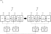
- FIG. 1 is a block diagram of an exemplary wireless power system 100 .
- the system 100 includes a wireless power transmitter 102 and a wireless power receiver 104 .
- a power source e.g., AC mains, battery, etc.
- Additional components can include power factor correction (PFC) circuit 106 before the inverter stage 108 .
- the inverter 108 drives the transmitter resonator coil and capacitive components 112 (“resonator”), via an impedance matching network 110 (including fixed and/or tunable network components).
- the transmitter resonator 112 produces an oscillating magnetic field which induces a voltage and/or current in receiver resonator 114 .
- the received energy is provided to a rectifier 118 via impedance matching network 116 (including fixed and/or tunable network components).
- the rectified power is provided to a load 120 (e.g., one or more batteries of an electric or hybrid vehicle).
- a load 120 e.g., one or more batteries of an electric or hybrid vehicle.
- the battery voltage level can impact various parameters (e.g., impedance) of the wireless power system 100 . Therefore, the battery voltage level may be received, determined, or measured to be provided as input to other portions of the wireless power system 100 .
- typical battery voltage ranges for electric vehicles include 200-280 V, 200-350 V, 200-420 V, etc.
- one or more components of the transmitter 102 can be coupled to a controller 122 , which may include a communication module (e.g., Wi-Fi, radio, Bluetooth, in-band signaling mechanism, etc.) configured to communicate with a communication module of receiver 104 .
- a communication module e.g., Wi-Fi, radio, Bluetooth, in-band signaling mechanism, etc.
- one or more components of the transmitter 102 can be coupled to one or more sensors 124 (e.g., a current sensor, a voltage sensor, a power sensor, a temperature sensor, a fault sensor, etc.).
- the controller 122 and sensor(s) 124 can be operably coupled to control portions of the transmitter 102 based on feedback signals from the sensor(s) 124 and/or sensor(s) 128 .
- one or more components of the receiver 104 can be coupled to a controller 126 , which may include a communication module (e.g., Wi-Fi, radio, Bluetooth, in-band signaling mechanism, etc.) configured to communicate with a communication module of transmitter 102 .
- a communication module e.g., Wi-Fi, radio, Bluetooth, in-band signaling mechanism, etc.
- one or more components of the transmitter 104 can be coupled to one or more sensors 128 (e.g., a current sensor, a voltage sensor, a power sensor, a temperature sensor, a fault sensor, etc.).
- the controller 126 and sensor(s) 128 can be operably coupled to control portions of the transmitter 102 based on feedback signals from the sensor(s) 128 and/or sensor(s) 124 .
- wireless power systems can be found in U.S. Patent Application Publication No. 2010/0141042, published Jun. 10, 2010 and titled “Wireless energy transfer systems,” and U.S. Patent Application Publication No. 2012/0112535, published May 10, 2012 and titled “Wireless energy transfer for vehicles,” both of which are hereby incorporated by reference in their entireties.
- High-power wireless power transmitters can be configured to transmit wireless power in applications such as powering of and/or charging a battery of vehicles, industrial machines, robots, or electronic devices relying on high power.
- the following disclosure focuses on wireless power transmission for vehicles. However, it is understood that any one or more of the embodiments described herein can be applied to other applications in which wireless power can be utilized.
- capacitor can refer to one or more electrical components having a capacitance (e.g., in Farads) and/or capacitive reactance (e.g., in Ohms).
- a capacitor may refer to one or more capacitors (e.g., in a “bank” of capacitors) that may be on the order of tens, hundreds, etc. of discrete capacitors. Two or more capacitors may be coupled in series or parallel to attain the desired capacitance and/or desired capacitive reactance.
- capacitive reactance may be expressed as a negative value herein. However, one skilled in the art would recognize that, in some conventions, capacitive reactance may also be expressed as a positive value.
- the term “inductor”, or the symbol therefor, can refer to one or more electrical components having a inductance (e.g., in Henries) and/or inductive reactance (e.g., in Ohms).
- an inductor may refer to one or more discrete inductors or coils. Two or more inductors may be coupled in series or parallel to attain a desired inductance and/or desired inductive reactance. Note that inductive reactance may be expressed as a positive value herein.
- the value of the components can be customized for the particular application.
- the value of various electronic components can depend whether the wireless power transmitter is used to transmit power for charging a vehicle battery (on the order of thousands of Watts) or a cell phone battery (typically less than 5 Watts).
- active rectification can enable a greater degree of control over power transmission to the output of the receiver 104 and/or load 120 . In some embodiments, active rectification can enable more efficient power transmission to the output of the receiver 104 and/or load 120 . In some embodiments, by employing active rectification in a wireless power receiver, the tunable impedance matching components in the receiver 104 and/or transmitter 102 can be eliminated. This can have the benefit of reducing the size, weight, and/or cost associated with the wireless power system.
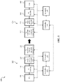
- FIG. 2A is a schematic of an exemplary wireless power system 200 leveraging active rectification.
- the exemplary system 200 includes a wireless power transmitter 202 .
- the exemplary transmitter 202 includes an inverter 206 (e.g., a half-bridge inverter, a full-bridge inverter, etc.) coupled to a filter circuit 207 (which can include, e.g., one or more inductive components L 3 s A, L 3 s B, one or more capacitive components, etc.).
- the inverter 206 can include two or more switches (e.g., transistors Q 1 , Q 2 , Q 3 , and Q 4 ).
- the switches Q 1 , Q 2 , Q 3 , Q 4 can be controlled via respective control signals PWM 1 , PWM 2 , PWM 3 , PWM 4 .
- the filter 207 can be further coupled to a transmitting resonator and/or matching circuit 208 (including capacitors C 2 s , C 1 s A, C 1 s B, and inductor L 1 s ), as described above.
- the inductor L 1 s of circuit 208 can be inductively coupled to the inductor L 1 d of receiving resonator and/or matching circuit 210 (including capacitors C 1 d A, C 1 d B, C 2 d , and inductor L 1 d ) so as to wirelessly transmit power from the transmitter 202 to the receiver 204 a .
- the transmitter coil L 1 s generates an oscillating magnetic field, which can induce an oscillating current at the receiver coil L 1 d .
- This current can have a frequency of, for example, 85 kHz.
- the current I 3 d can include harmonics due to the inverter 206 .
- characteristics (e.g., phase, amplitude, shape, harmonic content, etc.) of the current I 3 d can be further influenced (e.g., shaped, distorted, etc.) by one or more components of the receiver 204 a .
- circuits 210 and 212 can include inductive and/or capacitive components that can alter the phase or shape of the current I 3 d .
- the distortions of the current I 3 d can create challenges in operating the rectifier switches, as described further below.
- the exemplary receiver 204 a can include filter circuit 212 (including, e.g., one or more inductive components L 3 d A, L 3 d B, one or more capacitive components, etc.) coupled to the receiving resonator and/or matching circuit 210 .
- the filter circuit 212 can be configured to change characteristics (e.g., reduce distortions) of the current I 3 d.
- the filter circuit 212 can be coupled to the rectifier 214 a (e.g., a half-bridge inverter, a full-bridge inverter, etc.), which can include two or more switches (e.g., transistors Q 5 , Q 6 , Q 7 , and Q 8 ).
- the exemplary rectifier 214 a can be coupled directly or indirectly to a load 216 (e.g., a battery).
- a current sensor 218 can determine (e.g., measure, sense, etc.) the characteristics of the current I 3 d .
- the current sensor 218 can be coupled at the output of the filter 212 and/or input of the rectifier 214 .
- the current sensor 218 may determine the phase of the current I 3 d at the input of the rectifier 214 .
- the sensor signal may be provided to a processor and/or controller (e.g., controller 126 ) for processing.
- the processor and/or controller may generate control signals (e.g., PWM signals) for controlling one or more switches of the rectifier 214 based on the current sensor 218 signal(s).
- the processor and/or controller can provide the control signals (e.g., PWM 5 , PWM 6 , PWM 7 , PWM 8 ) to one or more switches (e.g., Q 5 , Q 6 , Q 7 , Q 8 , respectively) of the rectifier 214 .
- the current sensor 218 can include a zero-crossing detector configured to detect zero-crossings by the current I 3 d , as described in further detail below. The detector signal may be provided to the controller to determining the control signals for the switches.
- control signals may cause the rectifier switches to operate in various modes.
- the modes can include hard switching and/or soft switching (e.g., zero voltage switching).
- the rectifier switches can operate in one mode during a first time period and operate in another mode during a second time period. In some cases, the switches may alternate or transition between two modes during a given time period.
- FIG. 2B illustrates an alternative embodiment of a wireless power receiver 204 b including an active rectifier 214 b .
- Receiver 204 b includes the same or similar components described herein for receiver 204 a .
- the rectifier 214 b is a full-bridge active rectifier having diodes D 5 , D 6 in the high-side positions and switches Q 7 , Q 8 in the low-side positions.
- FIG. 2C illustrates another alternative embodiment of a wireless power receiver 204 c including an active rectifier 214 c .
- Receiver 204 c includes the same or similar components described herein for receiver 204 a .
- the rectifier 214 c is a full-bridge active rectifier having (i) diodes D 6 , D 8 coupled between input node 220 and the output of the rectifier 214 c and (ii) switches Q 5 , Q 7 coupled between input node 222 and the output of the rectifier 214 c .
- an active rectifier can be a full-bridge active rectifier having (i) switches Q 6 , Q 8 (replacing diodes D 6 , D 8 in FIG.
- FIG. 3A is a schematic of an exemplary wireless power system 300 utilizing active rectification.
- the system 300 can include components of system 200 (e.g., rectifier 214 a , 214 b , or 214 c ) as discussed above.
- system 300 can include a receiver 303 having one or more capacitors C 3 d A coupled between inductor L 3 d A and a first input 301 a of the rectifier 214 a and one or more capacitors C 3 d B coupled between L 3 d B and a second input 301 b of the rectifier 214 a.
- FIG. 3B illustrates an exemplary workflow 302 corresponding to exemplary method for determining the control signals (e.g., PWM 5 , PWM 6 , PWM 7 , PWM 8 ) for the rectifier switches (e.g., Q 5 , Q 6 , Q 7 , Q 8 , respectively) based on the input current I 3 d .
- FIG. 3C is a set of plots illustrating various signals in the generation of the control signals as a function of time.
- FIG. 3D illustrates an exemplary method 304 for determining control signals for active rectification in a rectifier presenting a resistive impedance to one or more portions of the wireless power system (e.g., the transmitter 202 , components between Vbus and arrow 305 , etc.).
- FIGS. 3A-3D are discussed together herein.
- the current I 3 d can be inputted to zero-crossing detector 306 (e.g., of control system 322 ).
- An exemplary current I 3 d is provided in FIG. 3C (i).
- the detector 306 is configured to detect the zero-crossing(s) of the input current I 3 d .
- the detector 306 can output a zero-crossing detection signal Vzcd indicating the zero-crossings of current signal I 3 d .
- the current I 3 d has a rising zero-crossing at time t 0 and a falling zero-crossing at time t 5 .
- Zero-crossing information can be used to synchronize switching patterns of Q 5 , Q 6 , Q 7 , and/or Q 8 switches to the I 3 d current zero-crossings, as illustrated in FIG. 3C (iii) and FIG. 3C (v).
- the rising edge 310 a (at time t 0 ) and falling edge 310 b (at time t 5 ) of signal Vzcd can be used to time the switching signals PWM pdt5 and PWM pdt7 (as illustrated in FIG. 3C (iii)) and the switching signals PWM pdt6 and PWM pdt8 (as illustrated in FIG. 3C (v)).
- the signal having the zero-crossing information can be provided to a delay block 312 (e.g., of control system 322 ).
- the delay block 312 can determine a first delay time T del1 and a second delay time T del2 based on system parameter(s) (e.g., ⁇ , as described further below).
- switch Q 5 should not be on at the same time as its pair, switch Q 7 .
- these time delays can be used to generate delayed control signals (e.g., PWM pdt5 , PWM pdt6 , PWM pdt7 , PWM pdt8 ).
- the delayed control signals can be provided to a dead-time compensation block 306 .
- Parameter ⁇ can be determined by a controller depending on a preferred system optimization.
- the controller may be configured to create an equivalent impedance of the rectifier 214 and therefore select ⁇ to achieve that impedance.
- the controller may be configured to maintain the impedance of the rectifier despite the changes in battery voltage (at load 216 ) and therefore select ⁇ to achieve maintenance.
- the controller may be configured to maintain the power provided to the load 216 within a particular range and therefore select ⁇ to achieve maintenance of power.
- ⁇ may be selected to maintain desirable coil current (e.g., in L 1 d ) on the receiver side.
- T del1 can be from 0.5 of a period (T period ) to 0.75 of a period (T period ). In some embodiments, T del2 can be from 0.25 of a period (T period ) to 0.5 of a period (T period ).
- Delay time T del1 can be used for the control signals for switches Q 5 and Q 7 .
- Delay time T del2 can be used for the control switches for switches Q 6 and Q 8 . Note that switches Q 5 and Q 7 form soft-switching phase-leg, while switches Q 6 and Q 8 form hard-switching phase-leg.
- delay time T del1 is equivalent to the difference between time t 0 and t 6 and delay time T del2 is equivalent to the difference between t 0 and t 3 .
- control system 322 e.g., controller 318 and/or processor 320 coupled to the switches
- the rising and falling edges 310 a , 310 b of signal Vzcd are used to produce the respective edges 324 a , 324 b of signals PWM pdt5 and PWM pdt7 .
- control system 322 can generate the third and fourth “pre-dead time” control signals PWM pdt6 , PWM pdt8 for the third and fourth rectifier switches Q 6 , Q 8 , respectively, based on the second delay time T del2 .
- the rising and falling edges 310 a , 310 b of signal Vzcd are used to produce the respective edges 328 a , 328 b of signals PWM pdt6 and PWM pdt8 .
- the dead-time insertion block 330 can insert a dead time T dead between the first pre-dead time control signal and the second pre-dead time control signal, PWM pdt5 and PWM pdt7 , respectively.
- the control system 322 produces control signals PWM 5 , PWM 7 for respective rectifier switches Q 5 , Q 7 .
- the dead-time insertion block 330 can insert a dead time T dead between the third pre-dead time control signal and the fourth pre-dead time control signal, PWM pdt6 and PWM pdt8 , respectively.
- the control system 322 produces control signals PWM 6 , PWM 8 for respective rectifier switches Q 6 , Q 8 .
- control system 322 can provide control signals to the respective rectifier switches.
- control signal PWM 5 is generated for switch Q 5 ;
- control signal PWM 6 is generated for switch Q 6 ;
- control signal PWM 7 is generated for switch Q 7 ;
- control signal PWM 8 is generated for switch Q 8 .
- control signals PWM 7 and PWM 8 are provided to respective switch Q 7 and Q 8 only.
- control signals PWM 5 and PWM 7 are provided to respective switch Q 5 and Q 8 .
- the value of filter inductor L 3 d A in system 300 can be approximately 35 ⁇ H.
- Series compensating capacitor can be used to maintain the same impedance at 85 kHz as the 7 uH inductor.
- FIG. 4A illustrates a workflow 400 of an exemplary method for generating control signals for the rectifier switches based on input current I 3 d .
- FIG. 4B is a set of plots illustrating various signals in the generation of the control signals as a function of time.
- FIG. 4C illustrates an exemplary method 402 for generating the control signals for a rectifier presenting a resistive impedance to one or more portions of the wireless power system (e.g., the transmitter 202 , components between Vbus and arrow 305 , etc.).
- FIGS. 4A-4C are discussed together herein.
- the current I 3 d can be provided to zero-crossing detector 406 (e.g., of processor 320 ).
- An exemplary current I 3 d is provided in FIG. 4B (i).
- the zero-crossing detector 406 can detect the rising zero-crossing at time to of the rising input current signal I 3 d and the falling zero-crossing at time t 5 of the falling input current signal I 3 d .
- the zero-crossing detector 406 can output a voltage signal Vzcd having zero-crossing information of the current signal I 3 d.
- a phase delay lock (PLL) block 410 can generate a PLL signal based on the rising zero-crossing and the falling zero-crossing of current I 3 d .
- Block 410 outputs PLL signal “SYNC”, as illustrated in FIG. 4B (iii), which is a signal “synchronized” to the zero-crossing signal Vzcd such that signal SYNC is in phase with signal Vzcd.
- the SYNC signal may be a copy of the voltage signal Vzcd.
- the SYNC signal may have the same phase and/or frequency of the signal Vzcd with a magnitude different from voltage signal Vzcd.
- the rising edge of Vzcd corresponds to the rising edge of SYNC at time t 0 (indicated by arrow 412 a ) and the falling edge of Vzcd corresponds to the falling edge of SYNC at time t 5 (indicated by arrow 412 b ).
- the delay block 414 can determine a first delay time T del1 and a second delay time T del2 based on system parameter(s) (e.g., ⁇ as described further below).
- T dead can be sufficiently large so that no shoot-through condition occurs during phase lags and so that one transistor of a pair of transistors is conducting at a given time.
- switch Q 5 is not on at the same time as its pair, switch Q 7 .
- the delayed signal can be provided to a dead-time compensation block 428 .
- Parameter ⁇ can be determined by a controller depending on a preferred system optimization.
- the controller may be configured to create an equivalent impedance of the rectifier 214 and therefore select ⁇ to achieve that impedance.
- the controller may be configured to maintain the impedance of the rectifier despite the changes in battery voltage (at load 216 ) and therefore select ⁇ to achieve maintenance.
- the controller may be configured to maintain the power provided to the load 216 within a particular range and therefore select ⁇ to achieve maintenance of power. For the example provided in FIG. 4B , parameter ⁇ is selected to be 47 degrees.
- T del1 can be from 0.5 of a period (T period ) to 0.75 of a period (T period ). In some embodiments, T del2 can be from 0.25 of a period (T period ) to 0.5 of a period (T period ).
- Delay time T del1 can be used for the control signals for switches Q 5 and Q 7 .
- Delay time T del2 can be used for the control switches for switches Q 6 and Q 8 . Note that switches Q 5 and Q 7 form the soft-switching phase leg, while switches Q 6 and Q 8 form the hard-switching phase leg.
- delay time T del1 is equivalent to the difference between time t 0 and t 6 and delay time T del2 is equivalent to the difference between t 0 and t 3 .
- delay block 414 can generate the “pre-dead time” first and second control signals PWM pdt5 and PWM pdt7 , respectively for the first and second rectifier switches, Q 5 and Q 7 , respectively, based on the PLL signal SYNC and the first delay time T del1 .
- the rising and falling edges 420 a , 420 b of signal SYNC are used to produce the edges 420 a , 420 b of signals PWM pdt5 and PWM pdt8 .
- delay block 414 can generate the “pre-dead time” third and fourth control signals PWM pdt6 and PWM pdt8 , respectively for the third and fourth rectifier switches Q 6 and Q 8 , respectively, based on the PLL signal SYNC and the second delay time T del2 .
- the rising and falling edges 412 a , 412 b of signal SYNC are used to produce the edges 424 a , 424 b of signals PWM pdt6 and PWM pdt8 .
- dead-time compensation block 428 can insert a dead time T dead between the “pre-dead time” first control signal and the “pre-dead time” second control signal PWM pdt5 and PWM pdt7 , respectively.
- Dead-time insertion is illustrated in FIG. 4B (v).
- block 428 can insert a dead time T dead between the “pre-dead time” third control signal and the “pre-dead time” fourth control signal PWM pdt6 and PWM pdt8 , respectively.
- Dead-time insertion is illustrated in FIG. 4B (vii).
- the control system produces control signals PWM 6 , PWM 8 for respective rectifier switches Q 6 , Q 8 .
- control system 322 can provide control signals (e.g., PWM 5 , PWM 6 , PWM 7 , and PWM 8 ) to the respective rectifier switches (e.g., Q 5 , Q 6 , Q 7 , and Q 8 , respectively).
- control signal PWM 5 is generated for switch Q 5 ;
- control signal PWM 6 is generated for switch Q 6 ;
- control signal PWM 7 is generated for switch Q 7 ; and control signal PWM 8 is generated for switch Q 8 .
- control signals PWM 7 and PWM 8 are provided to respective switch Q 7 and Q 8 only.
- control signals PWM 5 and PWM 7 are provided to respective switch Q 5 and Q 8 .
- the value of filter inductors L 3 s A, L 3 s B in method 402 can be approximately 14 ⁇ H. Note that the filter inductors L 3 s A, L 3 s B of method 402 is approximately five times less in value as the filter inductors L 3 s A, L 3 s B of method 304 . This can result in a reduced footprint (e.g., size, volume, etc.) and/or cost for a system employing method 402 .
- FIG. 5A illustrates a workflow 500 corresponding to an exemplary method for generating the control signals for the rectifier switches based on input current I 3 d .
- FIG. 5B is a set of plots illustrating various signals in the generation of the control signals as a function of time.
- FIG. 5C illustrates an exemplary active rectification method 502 in a rectifier presenting a capacitive impedance to one or more portions of the wireless power system (e.g., the transmitter 202 , components between Vbus and arrow 305 , etc.).
- FIGS. 5A-5C are discussed together herein.
- a sensor 506 can receive the input current I 3 d .
- sensor 506 can include a filter (e.g., a bandpass filter, a low-pass filter, a high-pass filter, etc.).
- the exemplary sensor 506 includes a bandpass filter characterized by the following transfer function:
- H ⁇ ( s ) ⁇ 0 Q f ⁇ s s 2 + ⁇ 0 Q f ⁇ s + ⁇ 0 2
- ⁇ 0 2* ⁇ /T period
- Qf is the quality factor of the filter.
- the filtering of the current I 3 d may stabilize the modulator and thereby enable stable output control (PWM) signals.
- the filtered current signal I 3 dmf is then provided to a zero-crossing detector 508 .
- the zero-crossing detector 508 can detect the rising zero-crossing of the filtered current signal I 3 dmf and the falling zero-crossing of the filtered current signal I 3 dmf .
- the detector 508 can produce an output signal ZCD (e.g., a voltage Vzcd and/or current Izcd) having zero-crossing information.
- ZCD e.g., a voltage Vzcd and/or current Izcd
- edge 512 a of signal ZCD corresponds to the rising zero-crossing of signal I 3 dmf (at time t 0 )
- edge 512 b of signal ZCD corresponds to falling zero-crossing of signal I 3 dmf (at time t 4 ).
- delay block 516 can determine a delay time T del1 based on system parameter(s) (e.g., ⁇ as described further below).
- the delayed signals PWM pdt5 , PWM pdt7 can be provided to a dead-time compensation block 518 .
- Parameter ⁇ can be determined by a controller depending on a preferred system optimization.
- the controller may be configured to create an equivalent impedance of the rectifier 214 and therefore select ⁇ to achieve that impedance.
- the controller may be configured to maintain the impedance of the rectifier constant despite the changes in battery voltage (at load 216 ) and therefore select ⁇ to achieve maintenance.
- the controller may be configured to maintain the power provided to the load 216 within a particular range and therefore select ⁇ to achieve maintenance of power. In the example provided in FIG. 5B , parameter ⁇ was selected to be 75 degrees.
- the delay block 516 can generate the “pre-dead time” first and second control signals PWM pdt5 and PWM pdt7 , respectively, for the first and second rectifier switches Q 5 and Q 7 , respectively, based on the delay time T del1 .
- delay time T de1l is equivalent to the difference between time t 0 and t 5 .
- the rising and falling edges 512 a , 512 b of signal ZCD are used to produce the edges 522 a , 522 b of signals PWM pdt5 and PWM pdt7 .
- dead-time insertion block 526 can include inserting a dead time T dead between the “pre-dead time” first control signal and the “pre-dead time” second control signal.
- the control system 322 produces control signals PWM pdt5 and PWM pdt7 for respective rectifier switches Q 5 , Q 7 .
- control system 322 can provide control signals PWM 5 , PWM 7 to the respective rectifier switches Q 5 , Q 7 (e.g., of rectifier 214 c ).
- the exemplary method 502 can enable the use of a smaller inductor at filter inductors L 3 s A, L 3 s B, thereby reducing the physical volume of the receiver 204 .
- the exemplary method 502 may also achieve greater efficiency as compared to methods which include the active control of four switches (e.g., Q 5 , Q 6 , Q 7 , and Q 8 ) of the rectifier 214 .
- FIG. 6A illustrates a workflow 600 for an exemplary method for generating control signals for rectifier switches by controlling the relative phase shift between input current I 3 d and input voltage V AC (also referred to as Vacd).
- FIGS. 6B-6C are a set of plots illustrating the generation of control signals as a function of time according to workflow 600 .
- FIG. 6D illustrates a method 602 for generating control signals according to the workflow 600 . Note that the control scheme of method 602 may be implemented in the mixed signal or digital domain. For the sake of clarity and conciseness, FIGS. 6A-6D are discussed together herein.
- current I 3 d can be inputted to a zero-crossing detector 604 (e.g., of control system 322 ).
- An exemplary current I 3 d is provided in FIG. 6B (v).
- detector 604 is configured to detect the zero-crossing(s) of input current I 3 d .
- the detector 604 can output a zero-crossing detection signal Vzcd indicating the zero-crossings of the current signal I 3 d .
- zero-crossing information can be used to synchronize the switching patterns of switches Q 5 , Q 6 , Q 7 , and/or Q 8 to the current zero-crossings.
- a phase delay lock (PLL) block 610 can generate a PLL signal based on the rising zero-crossing and the falling zero-crossing of current I 3 d .
- Block 610 outputs PLL signal “SYNC”, as illustrated in FIG. 6B (ii), which is a signal “synchronized” to the zero-crossing signal Vzcd such that signal SYNC is in phase with signal Vzcd.
- the SYNC signal may have a frequency at least two times the frequency of the voltage signal Vzcd.
- the SYNC signal may have a magnitude different from voltage signal Vzcd.
- the rising edge of Vzcd corresponds to a falling edge of SYNC (indicated by arrow 612 a ) and the falling edge of Vzcd corresponds to the rising edge of SYNC (indicated by arrow 612 b ) such that one period of signal Vzcd corresponds to two periods of signal SYNC.
- the ramp generation block 616 (e.g., of control system 322 ) can generate at least one ramp signal Vramp based on the output PLL signal.
- Ramp signal Vramp is used to produce PWM signals with the help of Vdc 1 and Vdc 2 defined with the following relationships:
- parameter ⁇ is selected to control the resistive impedance of the rectifier and is selected according to desired system optimization (as described above) and parameter ⁇ is selected to control the capacitive impedance of the rectifier.
- the PWM generator 620 (e.g., of control 622 ) can generate pre-dead time PWM signals PWM pdt5 , PWM pdt6 , PWM pdt6 , PWM pdt8 for switches Q 5 , Q 6 , Q 7 , Q 8 based on the signals Vdc 1 and Vdc 2 .
- the control system e.g., the modulator of system 322
- the frequency of the pre-dead time PWM signals is divided. In some embodiments, the frequency is divided by a factor of 2. In some embodiments, the frequency is divided by a factor greater than 2 (e.g., 2.5, 3, 4, etc.).
- dead-time compensation block 626 can insert a dead time T dead between the pre-dead time first control signal PWM pdt5 and the pre-dead time second control signal PWM pdt7 .
- the control system 322 produces control signals PWM 5 , PWM 7 for respective rectifier switches Q 5 , Q 7 .
- step 628 block 626 can insert a dead time T dead between the pre-dead time third control signal PWM pdt6 and the “pre-dead time” fourth control signal PWM pdt8 .
- the control system produces control signals PWM 6 , PWM 8 for respective rectifier switches Q 6 , Q 8 .
- control system 322 can provide control signals (e.g., PWM 5 , PWM 6 , PWM 7 , and PWM 8 ) to the respective rectifier switches (e.g., Q 5 , Q 6 , Q 7 , and Q 8 , respectively).
- control signal PWM 5 is generated for switch Q 5 ;
- control signal PWM 6 is generated for switch Q 6 ;
- control signal PWM 7 is generated for switch Q 7 ; and control signal PWM 8 is generated for switch Q 8 .
- control signals PWM 7 and PWM 8 are provided to respective switch Q 7 and Q 8 only.
- control signals PWM 5 and PWM 7 are provided to respective switch Q 5 and Q 8 .
- a wireless power system may be configured such that wireless power is transmitted from a transmitter to a receiver (also referred to as “unidirectional”).
- a wireless power system may be configured such that wireless power is transmitted from a first device to a second device (e.g., from a transmitter to a receiver) and/or from a second device to the first device (e.g., from a receiver to transmitter).
- Examples of bidirectional wireless power systems and methods can be found in U.S. Publication No. 2019/0006836 titled “Protection and control of wireless power systems” and published Jan. 3, 2019, and U.S. Publication No. 2020/0094696 titled “Wireless power transmission in electric vehicles” and published Mar. 26, 2020.
- FIG. 7 shows a schematic of an exemplary bidirectional wireless power system 700 .
- the schematic depicts both a transmitter (Tx) side wireless power device 700 a and a receiver (Rx) side wireless power device 700 b .
- the Tx-side wireless power device 700 a generally operates as a wireless power transmitter for the case of a similar unidirectional wireless power system (e.g., system 200 or 300 ).
- the Tx-side device 700 a may also be referred to as a ground assembly (GA) or GA-side device when used in the context of a wireless power device coupled to an electric vehicle or other mobile vehicle.
- G ground assembly
- the Tx-side refers generally to a wireless power device that is coupled to or configured to be coupled to a stationary power supply or load such as a power grid, AC generator, etc.
- the Tx-side system is generally capable of handling higher power, voltage, or current transients than the Rx-side wireless power device 700 b .
- the Rx-side wireless power device 700 b generally operates as a wireless power receiver for the case of a similar unidirectional wireless power transfer system (e.g., system 200 or 300 ).
- the Rx-side refers generally to a wireless power device that is coupled to or configured to be coupled to a mobile (or generally more limited) power supply or load such as a battery or a battery powered device (e.g., a computing device or an electric vehicle).
- a mobile or generally more limited
- the Rx-side wireless power device 700 b can also be referred to as a vehicle assembly (VA) or VA-side device when used in the context of a wireless power device coupled to an electric vehicle or other mobile vehicle.
- VA vehicle assembly
- both the Tx-side device 700 a and the Rx-side device 700 b include an inverter-rectifier 702 .
- the inverter-rectifier 702 can include a bridge configuration of switching elements and/or diodes.
- the inverter-rectifier 702 can include active switching elements, such as MOSFETs, which permit the inverter-rectifier 702 to operate as either an inverter or a rectifier in a bidirectional system.
- the operating mode (also referred to herein as an “operating personality”) of the inverter-rectifier 702 can be controlled based on the pattern of PWM control signals supplied to the switching elements.
- the inverter-rectifier 702 may be operated according to one or more active rectification methods (e.g., method 304 , 402 , 502 , and/or 602 ) described herein.
- the system 700 is able to power a load with power transmission in a first direction (e.g., a normal power flow direction from transmitter 700 a to receiver 700 b ), such as a battery of a vehicle, off of power input to the transmitter 700 a .
- a first direction e.g., a normal power flow direction from transmitter 700 a to receiver 700 b
- the system 700 can supply power in a second direction (e.g., a reverse power flow direction), such as suppling power to a power grid coupled to the Tx-side device 700 a from a battery of an electric vehicle coupled to the Rx-side device 700 b .
- the bidirectional system 700 can be used to power a home during a power outage from a battery of an electric vehicle battery parked in a garage.
- controller 122 a and 122 b can be combined in a single controller 720 .
- controller 126 a and 126 b can be combined in a single controller 740 .
- the controllers 720 and 740 include a bidirectional manager.
- the bidirectional manager coordinates the configuration of different hardware and software components wireless power device (e.g., either 700 a or 700 b ) according to the direction of power flow as indicated by an operating personality assigned to the device.
- an operating personality of INV indicates that the inverter-rectifier is operating as an inverter and therefore the wireless power device 700 a / 700 b is operating as a transmitter.
- an operating personality of REC indicates that the inverter-rectifier is operating as a rectifier and therefore the wireless power device 700 a / 700 b is operating as a receiver.
- the bidirectional manager also coordinates transitions from one direction of power flow to the opposite direction of power flow.
- the bidirectional manager of the Rx-side device 700 b can communicate with the bidirectional manager of the Rx-side device 700 a through a wireless communication link 750 (e.g., a Wi-Fi link) to coordinate a power reversal.
- the bidirectional manger can be implemented as separate controller within each device 700 a / 700 b or in software.
- various hardware and software components of the system can have different operating setpoints, modes and/or ranges of operations depending on the direction of flow of power, and by extension, the operating personality of the wireless power device 700 a / 700 b .
- the various operating set points, modes and/or ranges of operation can be stored in memory or in hardware.
- Each component of the system e.g. the inverter-rectifier 702 , tunable matching network (TMN) 703 , and other components
- TNN tunable matching network
- controllers, filters, communication systems, and/or protection systems can assume a different “operating personality” depending on the direction of power flow.
- the wireless power device's bidirectional manager can assign an appropriate personality at system startup and/or during a power flow transition based on the expected direction of power flow through the wireless power system 700 as a whole. For example, upon receipt of a command to switch from one mode of operation for the system to another (for example, by an operator interface, and/or user interface connected to either or all of the controllers, on either or both sides of the system or off system, such as on a network, the grid, or a mobile device), the bidirectional manager can assign the various component controllers (e.g., 122 a , 122 b , 126 a , and 126 b ) a respective operating personality.
- the various component controllers e.g., 122 a , 122 b , 126 a , and 126 b
- Each controller can use the assigned operating personality to identify and load appropriate operating processes or software code to control associated components of the wireless power transfer device 700 a / 700 b .
- an inverter-rectifier controller is assigned an operating personality of an inverter (e.g., INV)
- the controller will load software code to generate PWM control signal patterns to operate the inverter-rectifier switching elements to generate AC output signals from a DC input signal.
- an inverter-rectifier controller is assigned an operating personality of a rectifier (e.g., REC)
- the controller will load software code to generate PWM control signal patterns to operate the inverter-rectifier switching elements to rectify an AC input signal into a DC output signal.
- the bidirectional manager can provide the power demand, the power flow direction, choose the appropriate software code blocks, and assign personalities to sub-controllers or other controller(s).
- the bidirectional manager can determine the errors that are recoverable or not recoverable, depending on the side the system the controller is located on, and the operating personality it assumes for components of the system.
- the operational personalities can be assigned based on the expected power flow direction, e.g. vehicle-to-grid (V2G) power flow, or grid-to-vehicle (G2V) power flow.
- the bidirectional manager can determine the time and/or mode for recovery for those errors and/or clear errors when they are recovered so no user intervention is needed.
- the bidirectional manager can communicate with the user, the controller(s) of the other side of the system (e.g., the bidirectional manager on the other side of the system).
- the bidirectional manager can receive notification of an error from a component of the wireless power system and the error messages can be allocated to other components of the wireless power system, either directly by the bidirectional manager or after a callback request from the components.
- the bidirectional manager can receive communication from components of the wireless power system (e.g., via Wi-Fi from components from the other side of the system).
- the bidirectional manager can fulfill callback requests from components for messages related to the component, or can allocate the message to the relevant components.
- the bidirectional manager can control, including dynamically, the privileges of the components of the wireless power system to receive and send error and communication messages.
- the bidirectional manager can be responsible for controlling the components of the wireless power system during the transition phases, including handling any error conduction arising from the change of power transfer direction (both V2G and G2V transitions). For example, the bidirectional manager can oversee turning down of power, confirm power has fully or partially turned off, and sequence the components of the system to turn on (while assigning personalities to the components).
- the bidirectional manager on the transmitter controller receives a command to turn on power from idle, the bidirectional manager may assign G2V personality to the various controllers and hardware in the system.
- the bidirectional manager Upon receipt of a communication to change the power transmission direction, the bidirectional manager communicates between the transmitter and receiver to change power transmission direction.
- the bidirectional manager can be responsible for handling any error arising from the change of power transmission direction, including during the power down of the first direction and the power up of the second direction.
- the bidirectional manager can assign personality to the controller(s), for example, by selecting a subset of instructions from a non-transitory computer readable medium, or causing the controller(s) to select the subset of instructions.
- each controller of the system can contain a bidirectional manager.
- the bidirectional manager can operate as a top-level manager.
- assigning a personality to components/controllers can allow for modularity, non-redundant parts, code, and memory, allows for faster and on-the-fly switchover from G2V (grid-to-vehicle power flow) to V2G (vehicle-to-grid power flow) and back.
- FIG. 8 depicts flowchart of an exemplary bidirectional control process 800 that can be executed in accordance with implementations of the present disclosure.
- the example process 800 can be implemented, for example, by the example wireless power systems disclosed herein.
- the process 800 can be executed between a bidirectional manager of a transmitter wireless power device 700 a and a bidirectional manager of a receiver wireless power device 700 b .
- Process 800 shows divided primary side operations 802 and secondary side 804 operations.
- the primary side operations 802 are performed by a receiver wireless power device 700 b while the secondary side operations 704 are performed by a Tx-side wireless power device 700 a .
- the receiver (or device-side) wireless power device 700 b may generally be coupled to a smaller capacity or more limited power source or load.
- Implementing the receiver wireless power device 700 b as a primary device may provide more precise control of the bidirectional control process 800 to prevent exceeding possible lower operating limits of the Rx-side system or its load/source.
- the example process 800 can be provided by one or more computer-executable programs executed using one or more computing devices, processors, or microcontrollers.
- the example process 800 , or portions thereof, can be provided by one or more programs executed by control circuitry of wireless power devices 700 a , 700 b.
- the primary device initiates a power flow transition within the wireless power system.
- the initiation may be prompted by a user input, or in some implementations by an automatic power transition determination performed by the primary device ( 806 ).
- the primary device can determine to shift power flow based on various criteria including, but not limited to, state of charge of a battery, time of day, and availability and/or demand of grid-power.
- a Rx-side wireless power device 700 b can be configured to initiate a power flow reversal process when a connected battery is above a threshold charge level and a loss of grid power occurs.
- a Rx-side wireless power device 700 b can be configured to initiate a power flow reversal process when a connected battery is above a threshold charge level and during a preset time of day.
- the Rx-side wireless power device 700 b can be configured reverse power flow in order to provide supplemental power to a home during peak load periods of a power grid (e.g., periods of high demand and/or high energy prices such as evenings).
- the secondary device can determine when to initiate a power flow transition, but would perform an additional step of requesting initiation of the power flow transition from the primary device.
- the primary device sends instructions to the secondary device to reverse the direction of power flow ( 808 ).
- the secondary device reconfigures for operating in the opposite power flow direction from its current operations ( 810 ). For example, if the secondary device was operating as a transmitter it will reconfigure for operation as a receiver. If the secondary device was operating as a receiver it will reconfigure for operation as a transmitter.
- the secondary device's bidirectional manager can coordinate controller operations within the secondary device to shut down power flow in the present direction by, for example, securing operation of the inverter-rectifier, shifting switches to disconnect a load/power supply (as appropriate), toggling bypass switches to dissipate residual currents within the secondary device, or a combination thereof.
- the secondary device assigns a new operating personality in accordance with the new power flow direction ( 812 ).
- the secondary device's bidirectional manager assigns a new operating personality to respective controllers within the secondary device as appropriate to the new direction of power flow.
- the bidirectional power manager can assign the new operating personality by toggling a flag bit (e.g., TMN_SIDE discussed in more detail below) to indicate operation as a transmitter/inverter or operation as a receiver/rectifier.
- the various secondary device controllers can reconfigure their respective operations.
- the controllers can load control algorithms (e.g., software code blocks) to perform operations according to the new power flow direction.
- a TMN controller can reset a TMN and load control code for generating appropriate TMN control signals for operation in according to the new power flow direction.
- the TMN may need to adjust set points (e.g., impedance values, impedance adjustment step sizes, and/or protection schemes) to accommodate power transfer in the new direction or to prepare for power ramp up in the new direction or both.
- power flow in a V2G mode may generally be lower than in a G2V mode, e.g., due to asymmetries between GA and VA side resonator coils and/or discharge constraints on a battery. Consequently, TMN and/or inverter-rectifier set points may be different for operating in a V2G mode vice a G2V mode.
- the secondary device e.g., the secondary device's inverter controller
- the secondary device can control the inverter-rectifier operation according to the new operating personality ( 814 ).
- an inverter-rectifier controller can load appropriate algorithms for generating PWM control signals for operating as an inverter when the secondary device is a transmitter and operating as a rectifier when the secondary device is a receiver.
- the specific inverter and rectifier operations are described in more detail below in reference to FIGS. 9 and 10 .
- the secondary device sends a reply to the primary device indicating its reconfiguration status ( 816 ).
- the primary device waits and/or resends an instruction 808 .
- the process 800 may provide for safer and more robust operations. For example, it may prevent the power flow from commencing or reversing with mismatched personalities assigned to either the secondary or primary device.
- the primary device reconfigures for operating in the opposite power flow direction from its current operations ( 818 ). For example, if the primary device was operating as a transmitter it will reconfigure for operation as a receiver.
- the primary device If the primary device was operating as a receiver it will reconfigure for operation as a transmitter.
- the primary device's bidirectional manager can coordinate controller operations within the secondary device to shut down power flow in the present direction by, for example, securing operation of the inverter-rectifier, shifting switches to disconnect a load/power supply (as appropriate), toggling bypass switches to dissipate residual currents within the secondary device, or a combination thereof.
- the primary device assigns a new operating personality in accordance with the new power flow direction ( 820 ).
- the primary device's bidirectional manager assigns a new operating personality to respective controllers within the primary device as appropriate to the new direction of power flow.
- the bidirectional (power) manager can assign the new operating personality by toggling a flag bit (e.g., TMN_SIDE discussed in more detail below) to indicate operation as a transmitter/inverter or operation as a receiver/rectifier.
- the various primary device controllers can reconfigure their respective operations.
- the controllers can load control algorithms (e.g., software code blocks) to perform operations according to the new power flow direction.
- a TMN controller can reset a TMN and load control code for generating appropriate TMN control signals for operation in according to the new power flow direction.
- the TMN may need to adjust set points (e.g., impedance values and/or protection schemes) to accommodate power transfer in the new direction or to prepare for power ramp up in the new direction or both.
- the primary device can control the inverter-rectifier operation according to the new operating personality ( 822 ).
- an inverter-rectifier controller can load appropriate algorithms for generating PWM control signals for operating as an inverter when the secondary device is a transmitter and operating as a rectifier when the secondary device is a receiver.
- a TMN controller in the primary device can control the TMN according to the new operating personality.
- a TMN controller on the primary device can load appropriate control algorithms for generating TMN adjustment signals for operating as a load coupled TMN in a first direction, or a power supply coupled TMN in a second direction.
- FIG. 9 depicts a schematic 900 of an exemplary inverter-rectifier 902 and a timing diagram 902 illustrating operation of the inverter-rectifier in an inverter operating mode.
- the schematic 1800 shows a phase shifted full-bridge inverter.
- the inverter bridge circuit uses active switching elements Q 1 , Q 2 , Q 3 , and Q 4 , which can be, for example, MOSFETs, transistors, FETs, IGBTs, etc.
- the timing diagram 902 illustrates the driving signal pattern for the switches Q 1 , Q 2 , Q 3 , and Q 4 .
- the switches are grouped into two legs; Leg A (Q 1 , Q 3 ) and Leg B (Q 2 , Q 4 ).
- the corresponding switches in each leg are alternately switched on and off by respective PWM control signals.
- On time and off time, for each gate drive signal G 1 , G 2 , G 3 , and G 4 are shown.
- the dead time td shown is when both gate drivers of the same leg are off.
- the off time may be larger than the on time for each driving signal in a period Ts.
- the delay time tps between Leg A (Q 1 and Q 3 ) and Leg B (Q 2 and Q 4 ), when expressed in degrees, is known as the phase-shift angle and is a means for adjusting the overall power sourced by the inverter-rectifier when operating as an inverter.
- Total power output is controlled by adjusting the delay time tPS between the Leg A and Leg B PWM signals.
- the inverter-rectifier 900 may be operated according to one or more active rectification methods (e.g., method 304 , 402 , 502 , and/or 602 ) described herein.
- active rectification methods e.g., method 304 , 402 , 502 , and/or 602
- the inverter-rectifier switches can be arranged in a half-bridge configuration.
- the inverter-rectifier can implement zero-voltage switching operations to ensure the switches are operated when the voltage across them is zero or near-zero.
- FIG. 10 depicts a schematic 1000 of an exemplary inverter-rectifier and a timing diagram 1902 illustrating operation of the inverter-rectifier 702 in a rectifier operating mode.
- FIG. 10 illustrates a synchronous rectifier operation utilizing the same switches as shown in FIG. 9 .
- the gate drive signals (G 1 , G 2 , G 3 , G 4 ) corresponding to respective switches (Q 1 , Q 2 , Q 3 , Q 4 ) are shown in the timing diagram 1902 .
- zero current switching operation is shown, zero-voltage switching (ZVS) naturally follows the operation and can be used in some implementations. However, ZVS switching in active rectification mode is not shown in figures.
- the synchronous rectifier can receive the zero-crossing of the I 3 s current (shown as I 3 d or I 3 s in FIG. 7 ) and creates the timing of the synchronous rectification (zero current switching) as shown in timing diagram 1002 .
- the inverter-rectifier 702 rectifies an AC input signal into a DC output signal by alternately switching on corresponding pairs of switches (Q 1 /Q 4 and Q 2 /Q 3 ).
- the inverter-rectifier controller e.g., inverter/protection and control circuitry
- the switches Q 1 , Q 2 , Q 3 , and Q 4 can be turned off at the zero current (or near zero current) of the input to the inverter-rectifier 702 , and an appropriate time delay td may be permitted to lapse before operating the next pair of switches (e.g., Q 1 and Q 4 or Q 2 and Q 3 ). This can prevent power losses within the switch. In some implementations, the time delay may be adjusted by the system as needed.
- the inverter-rectifier does not begin does not begin switching until the measured input power is above a threshold value that ensures continuous conduction of the I 3 d current.
- the threshold value can be, e.g., between 2 kW and 4 kW, and/or between 20-40% of a target power.
- the input AC signal may be noisy, potentially resulting in inaccurate zero-crossing detections and possibly large transients for imprecise switching.
- the I 3 d current that is used to generate the PWM synchronization may be discontinuous and noisy resulting in inaccurate zero-crossing detections and possibly large transients or even in a destructive shorting of the power stage.
- rectification can be performed passively when power is below the threshold value by conduction through the body-diodes of the switches.
- the switching operations performed above the threshold input power value can be considered an active rectification mode and the body-diode conduction below the threshold input power value can be considered a passive rectification mode.
- the inverter-rectifier 1000 may be operated according to one or more active rectification methods (e.g., method 304 , 402 , 502 , and/or 602 ) described herein.
- active rectification methods e.g., method 304 , 402 , 502 , and/or 602
- some or all of the processing described above can be carried out on one or more centralized computing devices. In some examples, some types of processing occur on one device and other types of processing occur on another device. In some examples, some or all of the data described above can be stored in data storage hosted on one or more centralized computing devices, or via cloud-based storage. In some examples, some data are stored in one location and other data are stored in another location. In some examples, quantum computing can be used. In some examples, functional programming languages can be used. In some examples, electrical memory, such as flash-based memory, can be used.
- FIG. 11 is a block diagram of an example computer system 1100 that may be used in implementing the technology described in this document.
- General-purpose computers, network appliances, mobile devices, or other electronic systems may also include at least portions of the system 1100 .
- the system 1100 includes a processor 1110 , a memory 1120 , a storage device 1130 , and an input/output device 1140 .
- Each of the components 1110 , 1120 , 1130 , and 1140 may be interconnected, for example, using a system bus 1150 .
- the processor 1110 is capable of processing instructions for execution within the system 1100 .
- the processor 1110 is a single-threaded processor.
- the processor 1110 is a multi-threaded processor.
- the processor 1110 is capable of processing instructions stored in the memory 1120 or on the storage device 1130 .
- the memory 1120 stores information within the system 1100 .
- the memory 1120 is a non-transitory computer-readable medium.
- the memory 1120 is a volatile memory unit.
- the memory 1120 is a non-volatile memory unit.
- the storage device 1130 is capable of providing mass storage for the system 1100 .
- the storage device 1130 is a non-transitory computer-readable medium.
- the storage device 1130 may include, for example, a hard disk device, an optical disk device, a solid-date drive, a flash drive, or some other large capacity storage device.
- the storage device may store long-term data (e.g., database data, file system data, etc.).
- the input/output device 1140 provides input/output operations for the system 1100 .
- the input/output device 1140 may include one or more of a network interface devices, e.g., an Ethernet card, a serial communication device, e.g., an RS-232 port, and/or a wireless interface device, e.g., an 802.11 card, a 3G wireless modem, or a 4G wireless modem.
- the input/output device may include driver devices configured to receive input data and send output data to other input/output devices, e.g., keyboard, printer and display devices 1160 .
- mobile computing devices, mobile communication devices, and other devices may be used.
- At least a portion of the approaches described above may be realized by instructions that upon execution cause one or more processing devices to carry out the processes and functions described above.
- Such instructions may include, for example, interpreted instructions such as script instructions, or executable code, or other instructions stored in a non-transitory computer readable medium.
- the storage device 1130 may be implemented in a distributed way over a network, such as a server farm or a set of widely distributed servers, or may be implemented in a single computing device.
- Embodiments of the subject matter described in this specification can be implemented as one or more computer programs, i.e., one or more modules of computer program instructions encoded on a tangible nonvolatile program carrier for execution by, or to control the operation of, data processing apparatus.
- the program instructions can be encoded on an artificially generated propagated signal, e.g., a machine-generated electrical, optical, or electromagnetic signal that is generated to encode information for transmission to suitable receiver apparatus for execution by a data processing apparatus.
- the computer storage medium can be a machine-readable storage device, a machine-readable storage substrate, a random or serial access memory device, or a combination of one or more of them.
- system may encompass all kinds of apparatus, devices, and machines for processing data, including by way of example a programmable processor, a computer, or multiple processors or computers.
- a processing system may include special purpose logic circuitry, e.g., an FPGA (field programmable gate array) or an ASIC (application specific integrated circuit).
- a processing system may include, in addition to hardware, code that creates an execution environment for the computer program in question, e.g., code that constitutes processor firmware, a protocol stack, a database management system, an operating system, or a combination of one or more of them.
- a computer program (which may also be referred to or described as a program, software, a software application, a module, a software module, a script, or code) can be written in any form of programming language, including compiled or interpreted languages, or declarative or procedural languages, and it can be deployed in any form, including as a standalone program or as a module, component, subroutine, or other unit suitable for use in a computing environment.
- a computer program may, but need not, correspond to a file in a file system.
- a program can be stored in a portion of a file that holds other programs or data (e.g., one or more scripts stored in a markup language document), in a single file dedicated to the program in question, or in multiple coordinated files (e.g., files that store one or more modules, sub programs, or portions of code).
- a computer program can be deployed to be executed on one computer or on multiple computers that are located at one site or distributed across multiple sites and interconnected by a communication network.
- the processes and logic flows described in this specification can be performed by one or more programmable computers executing one or more computer programs to perform functions by operating on input data and generating output.
- the processes and logic flows can also be performed by, and apparatus can also be implemented as, special purpose logic circuitry, e.g., an FPGA (field programmable gate array) or an ASIC (application specific integrated circuit).
- special purpose logic circuitry e.g., an FPGA (field programmable gate array) or an ASIC (application specific integrated circuit).
- Computers suitable for the execution of a computer program can include, by way of example, general or special purpose microprocessors or both, or any other kind of central processing unit.
- a central processing unit will receive instructions and data from a read-only memory or a random access memory or both.
- a computer generally includes a central processing unit for performing or executing instructions and one or more memory devices for storing instructions and data.
- a computer will also include, or be operatively coupled to receive data from or transfer data to, or both, one or more mass storage devices for storing data, e.g., magnetic, magneto optical disks, or optical disks.
- mass storage devices for storing data, e.g., magnetic, magneto optical disks, or optical disks.
- a computer need not have such devices.
- Computer readable media suitable for storing computer program instructions and data include all forms of nonvolatile memory, media and memory devices, including by way of example semiconductor memory devices, e.g., EPROM, EEPROM, and flash memory devices; magnetic disks, e.g., internal hard disks or removable disks; magneto optical disks; and CD-ROM and DVD-ROM disks.
- semiconductor memory devices e.g., EPROM, EEPROM, and flash memory devices
- magnetic disks e.g., internal hard disks or removable disks
- magneto optical disks e.g., CD-ROM and DVD-ROM disks.
- the processor and the memory can be supplemented by, or incorporated in, special purpose logic circuitry.
- Embodiments of the subject matter described in this specification can be implemented in a computing system that includes a back end component, e.g., as a data server, or that includes a middleware component, e.g., an application server, or that includes a front end component, e.g., a client computer having a graphical user interface or a Web browser through which a user can interact with an implementation of the subject matter described in this specification, or any combination of one or more such back end, middleware, or front end components.
- the components of the system can be interconnected by any form or medium of digital data communication, e.g., a communication network. Examples of communication networks include a local area network (“LAN”) and a wide area network (“WAN”), e.g., the Internet.
- LAN local area network
- WAN wide area network
- the computing system can include clients and servers.
- a client and server are generally remote from each other and typically interact through a communication network.
- the relationship of client and server arises by virtue of computer programs running on the respective computers and having a client-server relationship to each other.
- X has a value of approximately Y” or “X is approximately equal to Y”
- X should be understood to mean that one value (X) is within a predetermined range of another value (Y).
- the predetermined range may be plus or minus 20%, 10%, 5%, 3%, 1%, 0.1%, or less than 0.1%, unless otherwise indicated.
- a reference to “A and/or B”, when used in conjunction with open-ended language such as “comprising” can refer, in one embodiment, to A only (optionally including elements other than B); in another embodiment, to B only (optionally including elements other than A); in yet another embodiment, to both A and B (optionally including other elements); etc.
- At least one of A and B can refer, in one embodiment, to at least one, optionally including more than one, A, with no B present (and optionally including elements other than B); in another embodiment, to at least one, optionally including more than one, B, with no A present (and optionally including elements other than A); in yet another embodiment, to at least one, optionally including more than one, A, and at least one, optionally including more than one, B (and optionally including other elements); etc.
- ordinal terms such as “first,” “second,” “third,” etc., in the claims to modify a claim element does not by itself connote any priority, precedence, or order of one claim element over another or the temporal order in which acts of a method are performed. Ordinal terms are used merely as labels to distinguish one claim element having a certain name from another element having a same name (but for use of the ordinal term), to distinguish the claim elements.
Landscapes
- Engineering & Computer Science (AREA)
- Power Engineering (AREA)
- Computer Networks & Wireless Communication (AREA)
- Transportation (AREA)
- Mechanical Engineering (AREA)
- Rectifiers (AREA)
- Charge And Discharge Circuits For Batteries Or The Like (AREA)
- Dc-Dc Converters (AREA)
- Selective Calling Equipment (AREA)
Abstract
Description
-
- The transmitter coil L1 s can be disposed on a single or multiple layers of ferrite.
- The system 200 is configured to deliver approximately 11.3 kW of power to the
load 216. - The receiver coil L1 d can have 15 or less turns, 20 or less turns, 25 or less turns, etc. (e.g., approximately 16 turns).
- The matching can be configured for a voltage range Vbus=300-900 V (e.g., 640-840 V).
Time delay 1: T del1=(270−β)/360*T period
Time delay 2: T del2=(90+β)/360*T period −T dead
where 0≤β≤90°, Tperiod is a single period in time of the input signal I3 d, and time Tdead is a fixed quantity (e.g., on the order of hundreds of nanoseconds) based on the specifications of the transistors and/or gate drivers used. Time Tdead can be sufficiently large so that no shoot-through condition occurs during phase lags and so that one transistor of a pair of transistors is conducting at a given time. For example, switch Q5 should not be on at the same time as its pair, switch Q7. As described below, these time delays can be used to generate delayed control signals (e.g., PWMpdt5, PWMpdt6, PWMpdt7, PWMpdt8). The delayed control signals can be provided to a dead-
Time delay 1: T del1=(270−β)/360*T period
Time delay 2: Tdel2=(90+β)/360*T period −T dead
where 0≤β≤90°, Tperiod is a single period in time of the input signal I3 d, and time Tdead is a fixed quantity based on the specifications of the transistors and/or gate drivers. Tdead can be sufficiently large so that no shoot-through condition occurs during phase lags and so that one transistor of a pair of transistors is conducting at a given time. For example, switch Q5 is not on at the same time as its pair, switch Q7. The delayed signal can be provided to a dead-
where ω0=2*π/Tperiod and Qf is the quality factor of the filter. The filtering of the current I3 d may stabilize the modulator and thereby enable stable output control (PWM) signals. The filtered current signal I3 dmf is then provided to a zero-crossing
Time delay: T del1=(270−β)/360*T period
where 0≤β≤90°, Tperiod is a single period in time of the input signal ZCD, and time Tdead is a fixed quantity based on the specifications of the transistors and/or gate drivers. Tdead can be sufficiently large so that no shoot-through condition occurs during phase lags and so that one transistor of a pair of transistors is conducting at a given time. For example, switch Q5 is not on at the same time as its pair, switch Q7. The delayed signals PWMpdt5, PWMpdt7 can be provided to a dead-time compensation block 518.
where parameter β is selected to control the resistive impedance of the rectifier and is selected according to desired system optimization (as described above) and parameter φ is selected to control the capacitive impedance of the rectifier. In the example provided in
Claims (18)
Priority Applications (2)
| Application Number | Priority Date | Filing Date | Title |
|---|---|---|---|
| US17/003,800 US11316375B2 (en) | 2019-08-26 | 2020-08-26 | Control of active rectification in wireless power systems |
| US17/700,243 US11843258B2 (en) | 2019-08-26 | 2022-03-21 | Bidirectional operation of wireless power systems |
Applications Claiming Priority (2)
| Application Number | Priority Date | Filing Date | Title |
|---|---|---|---|
| US201962891959P | 2019-08-26 | 2019-08-26 | |
| US17/003,800 US11316375B2 (en) | 2019-08-26 | 2020-08-26 | Control of active rectification in wireless power systems |
Related Child Applications (1)
| Application Number | Title | Priority Date | Filing Date |
|---|---|---|---|
| US17/700,243 Continuation US11843258B2 (en) | 2019-08-26 | 2022-03-21 | Bidirectional operation of wireless power systems |
Publications (2)
| Publication Number | Publication Date |
|---|---|
| US20210066968A1 US20210066968A1 (en) | 2021-03-04 |
| US11316375B2 true US11316375B2 (en) | 2022-04-26 |
Family
ID=72433025
Family Applications (2)
| Application Number | Title | Priority Date | Filing Date |
|---|---|---|---|
| US17/003,800 Active US11316375B2 (en) | 2019-08-26 | 2020-08-26 | Control of active rectification in wireless power systems |
| US17/700,243 Active US11843258B2 (en) | 2019-08-26 | 2022-03-21 | Bidirectional operation of wireless power systems |
Family Applications After (1)
| Application Number | Title | Priority Date | Filing Date |
|---|---|---|---|
| US17/700,243 Active US11843258B2 (en) | 2019-08-26 | 2022-03-21 | Bidirectional operation of wireless power systems |
Country Status (7)
| Country | Link |
|---|---|
| US (2) | US11316375B2 (en) |
| EP (1) | EP4022739A1 (en) |
| JP (2) | JP7383131B2 (en) |
| KR (1) | KR102460384B1 (en) |
| CN (2) | CN116961250B (en) |
| IL (1) | IL290797B2 (en) |
| WO (1) | WO2021041574A1 (en) |
Families Citing this family (3)
| Publication number | Priority date | Publication date | Assignee | Title |
|---|---|---|---|---|
| US11196301B1 (en) * | 2020-12-16 | 2021-12-07 | Stmicroelectronics Asia Pacific Pte Ltd | Synchronous auto-zero comparator for wireless power rectifier |
| CN114070023A (en) * | 2021-11-01 | 2022-02-18 | 许继电源有限公司 | Method and system for synchronizing transmitting side and receiving side of wireless charging and discharging system |
| KR102669364B1 (en) | 2022-11-10 | 2024-05-27 | 경희대학교 산학협력단 | Simultaneous wireless information and power transfer system and operating method thereof |
Citations (3)
| Publication number | Priority date | Publication date | Assignee | Title |
|---|---|---|---|---|
| US20140292092A1 (en) * | 2013-03-29 | 2014-10-02 | Fuji Electric Co., Ltd. | Power supply device |
| US20150303703A1 (en) * | 2014-04-22 | 2015-10-22 | Toyota Jidosha Kabushiki Kaisha | Non-contact power transmitting and receiving system |
| US20200303926A1 (en) * | 2016-03-30 | 2020-09-24 | Byd Company Limited | Car charger and vehicle |
Family Cites Families (132)
| Publication number | Priority date | Publication date | Assignee | Title |
|---|---|---|---|---|
| GB1506633A (en) | 1974-05-21 | 1978-04-05 | Senger N | Electrical isolating circuits |
| ZA892468B (en) | 1988-04-11 | 1989-12-27 | Uniscan Ltd | Improvements in or relating to cutting elements foactuator and communication system r rotary drill bits |
| GB2309343B (en) | 1996-01-16 | 2000-05-03 | Cegelec Controls Ltd | Protection arrangement for a switching device |
| US5640082A (en) | 1996-01-31 | 1997-06-17 | Hughes Electronics | Duty cycle controlled switch variable capacitor circuit |
| US5784269A (en) | 1997-02-21 | 1998-07-21 | Lucent Technologies, Inc. | Three phase high power factor converter using phase selection circuit |
| JPH1127870A (en) | 1997-07-03 | 1999-01-29 | Toyota Autom Loom Works Ltd | Charge method, charging equipment, charger, and vehicle |
| JPH11127580A (en) | 1997-10-22 | 1999-05-11 | Yaskawa Electric Corp | Rectifying circuit |
| US6483730B2 (en) | 1999-08-13 | 2002-11-19 | Powerware Corporation | Power converters with AC and DC operating modes and methods of operation thereof |
| NZ337716A (en) | 1999-09-09 | 2002-10-25 | Auckland Uniservices Ltd | Series resonant inductive pickup where power can be regulated by time-regulated opening and closing a switch |
| WO2001080411A1 (en) | 2000-04-12 | 2001-10-25 | Wolfgang Croce | Switched-mode power supply |
| CA2502798C (en) | 2004-03-31 | 2011-06-14 | University Of New Brunswick | Single-stage buck-boost inverter |
| WO2006119362A2 (en) | 2005-05-03 | 2006-11-09 | Massachusetts Institute Of Technology | Methods and apparatus for resistance compression networks |
| KR101156616B1 (en) | 2005-07-12 | 2012-06-15 | 메사추세츠 인스티튜트 오브 테크놀로지 | Wireless non-radioactive energy transfer |
| US7825543B2 (en) | 2005-07-12 | 2010-11-02 | Massachusetts Institute Of Technology | Wireless energy transfer |
| TW200709544A (en) | 2005-08-29 | 2007-03-01 | Ind Tech Res Inst | Transformer-free power conversion circuit for parallel connection with commercial electricity system |
| US7276886B2 (en) | 2005-10-03 | 2007-10-02 | Texas Instruments Incorporated | Dual buck-boost converter with single inductor |
| JP2008277882A (en) | 2007-04-25 | 2008-11-13 | Matsushita Electric Ind Co Ltd | Amplifying circuit and radio communication device |
| NZ563188A (en) | 2007-11-05 | 2010-03-26 | Auckland Uniservices Ltd | Power control |
| US8855554B2 (en) | 2008-03-05 | 2014-10-07 | Qualcomm Incorporated | Packaging and details of a wireless power device |
| JP5152338B2 (en) | 2008-09-19 | 2013-02-27 | トヨタ自動車株式会社 | Non-contact charging device and non-contact power receiving device |
| CN102239633B (en) | 2008-09-27 | 2017-01-18 | 韦特里西提公司 | Wireless energy transfer systems |
| US8643326B2 (en) | 2008-09-27 | 2014-02-04 | Witricity Corporation | Tunable wireless energy transfer systems |
| US9515494B2 (en) | 2008-09-27 | 2016-12-06 | Witricity Corporation | Wireless power system including impedance matching network |
| US20120112535A1 (en) | 2008-09-27 | 2012-05-10 | Aristeidis Karalis | Wireless energy transfer for vehicles |
| US8598743B2 (en) | 2008-09-27 | 2013-12-03 | Witricity Corporation | Resonator arrays for wireless energy transfer |
| US20110074346A1 (en) | 2009-09-25 | 2011-03-31 | Hall Katherine L | Vehicle charger safety system and method |
| US9601266B2 (en) | 2008-09-27 | 2017-03-21 | Witricity Corporation | Multiple connected resonators with a single electronic circuit |
| US8742628B2 (en) | 2009-04-30 | 2014-06-03 | The United States Of America As Represented By The Secretary Of The Army | Solid state circuit breaker |
| CN105048643B (en) | 2010-02-08 | 2018-08-03 | 飞利浦知识产权企业有限公司 | input parasitic metal detection |
| US9561730B2 (en) * | 2010-04-08 | 2017-02-07 | Qualcomm Incorporated | Wireless power transmission in electric vehicles |
| US10343535B2 (en) | 2010-04-08 | 2019-07-09 | Witricity Corporation | Wireless power antenna alignment adjustment system for vehicles |
| JP4957827B2 (en) | 2010-04-14 | 2012-06-20 | トヨタ自動車株式会社 | Power supply system and vehicle equipped with the same |
| US20110260865A1 (en) | 2010-04-26 | 2011-10-27 | Sensormatic Electronics, LLC | Method for reducing metal detection system false alarms |
| US10079090B2 (en) | 2010-12-01 | 2018-09-18 | Triune Systems, LLC | Multiple coil data transmission system |
| US10090885B2 (en) | 2011-04-13 | 2018-10-02 | Qualcomm Incorporated | Antenna alignment and vehicle guidance for wireless charging of electric vehicles |
| US8749939B2 (en) | 2011-05-13 | 2014-06-10 | Mks Instruments, Inc. | Method and system for shoot-through protection |
| US9263968B2 (en) * | 2011-06-22 | 2016-02-16 | Eetrex, Inc. | Bidirectional inverter-charger |
| CA2848040C (en) | 2011-09-09 | 2019-08-13 | Witricity Corporation | Foreign object detection in wireless energy transfer systems |
| US20130062966A1 (en) | 2011-09-12 | 2013-03-14 | Witricity Corporation | Reconfigurable control architectures and algorithms for electric vehicle wireless energy transfer systems |
| JP5753906B2 (en) | 2011-09-29 | 2015-07-22 | 株式会社日立パワーソリューションズ | Charge control device and charge control method |
| US9145110B2 (en) | 2011-10-27 | 2015-09-29 | Ford Global Technologies, Llc | Vehicle wireless charger safety system |
| JP5838768B2 (en) | 2011-11-30 | 2016-01-06 | ソニー株式会社 | Sensing device, power receiving device, non-contact power transmission system, and sensing method |
| CN104054229B (en) | 2012-01-06 | 2018-01-23 | 捷通国际有限公司 | Wireless power receiver system |
| US9417199B2 (en) | 2012-01-17 | 2016-08-16 | Triune Systems, LLC | Method and system of wireless power transfer foreign object detection |
| JP5764082B2 (en) | 2012-03-06 | 2015-08-12 | 株式会社アドバンテスト | Wireless power receiving device, wireless power feeding device, and wireless power transmission system |
| US8830710B2 (en) | 2012-06-25 | 2014-09-09 | Eta Devices, Inc. | RF energy recovery system |
| US9287607B2 (en) | 2012-07-31 | 2016-03-15 | Witricity Corporation | Resonator fine tuning |
| US9190876B2 (en) | 2012-09-28 | 2015-11-17 | Qualcomm Incorporated | Systems and methods for detecting wireless charging transmit characteristics |
| KR101436063B1 (en) | 2012-10-18 | 2014-08-29 | (주)기술과가치 | Wiress Power Transmission Apparatus |
| US9404954B2 (en) | 2012-10-19 | 2016-08-02 | Witricity Corporation | Foreign object detection in wireless energy transfer systems |
| US9608454B2 (en) | 2012-12-03 | 2017-03-28 | WIPQTUS Inc. | Wireless power system with a self-regulating wireless power receiver |
| US9998180B2 (en) | 2013-03-13 | 2018-06-12 | Integrated Device Technology, Inc. | Apparatuses and related methods for modulating power of a wireless power receiver |
| DE102014208991A1 (en) | 2013-05-15 | 2014-11-20 | Ford Global Technologies, Llc | Security system for wireless vehicle charging device |
| CN103414255B (en) | 2013-06-05 | 2015-06-24 | 中国人民解放军国防科学技术大学 | Self-tuning magnetic-coupling resonance wireless energy transmission system and self-tuning method thereof |
| US10320234B2 (en) | 2013-08-02 | 2019-06-11 | Integrated Device Technology, Inc. | Multimode wireless power receivers and related methods |
| EP3039770B1 (en) | 2013-08-14 | 2020-01-22 | WiTricity Corporation | Impedance tuning |
| CN104426344B (en) | 2013-08-22 | 2017-11-14 | 全汉企业股份有限公司 | Buffer circuit and buffering method for buffer circuit |
| US9438064B2 (en) | 2013-08-30 | 2016-09-06 | Qualcomm Incorporated | System and method for alignment and compatibility detection for a wireless power transfer system |
| WO2015069122A1 (en) | 2013-11-11 | 2015-05-14 | Powerbyproxi Limited | Contactless power receiver and method for operating same |
| US9912196B2 (en) | 2013-12-10 | 2018-03-06 | The Chugoku Electric Power Co., Inc. | Power receiving device and power feeding system |
| US9815379B2 (en) | 2014-01-21 | 2017-11-14 | Qualcomm Incorporated | Systems and methods for electric vehicle induction coil alignment |
| EP3103126A4 (en) | 2014-02-07 | 2017-11-01 | PowerbyProxi Limited | Inductive power receiver with resonant coupling regulator |
| KR20160119842A (en) | 2014-02-23 | 2016-10-14 | 애플 인크. | Adjusting filter in a coupled coil system |
| JP2015159667A (en) | 2014-02-24 | 2015-09-03 | キヤノン株式会社 | power supply device |
| US9772401B2 (en) | 2014-03-17 | 2017-09-26 | Qualcomm Incorporated | Systems, methods, and apparatus for radar-based detection of objects in a predetermined space |
| DK3123592T3 (en) | 2014-03-27 | 2019-10-14 | Schneider Electric It Corp | Bi-directional DC-DC converter |
| JP6464520B2 (en) | 2014-04-23 | 2019-02-06 | パナソニックIpマネジメント株式会社 | Non-contact power transmission device, non-contact power reception device, and non-contact power transmission system |
| US9591739B2 (en) | 2014-05-02 | 2017-03-07 | Reno Technologies, Inc. | Multi-stage heterodyne control circuit |
| US9735585B2 (en) | 2014-05-05 | 2017-08-15 | Google Inc. | Foreign object detection method for wireless charging systems |
| EP3140680B1 (en) | 2014-05-07 | 2021-04-21 | WiTricity Corporation | Foreign object detection in wireless energy transfer systems |
| WO2015173847A1 (en) | 2014-05-14 | 2015-11-19 | ネオテス株式会社 | Contactless power transfer device |
| KR101519510B1 (en) | 2014-06-03 | 2015-05-12 | 주식회사 아이티엠반도체 | Identification module card having battery protection circuit module and portable wireless terminal including the same |
| JP2015231306A (en) | 2014-06-06 | 2015-12-21 | トヨタ自動車株式会社 | Non-contact power reception device |
| US9692251B2 (en) | 2014-07-03 | 2017-06-27 | Intel Corporation | Apparatus, system and method of wireless power transfer |
| KR101983173B1 (en) | 2014-09-11 | 2019-09-10 | 주식회사 위츠 | Non-contact type power receiving apparatus and non-contact type battery apparatus |
| US9784777B2 (en) | 2014-09-24 | 2017-10-10 | Qualcomm Incorporated | Methods and systems for measuring power in wireless power systems |
| US9782092B2 (en) | 2014-11-14 | 2017-10-10 | Siemens Medical Solutions Usa, Inc. | Patient signal analysis based on vector analysis |
| US10012725B2 (en) | 2014-12-19 | 2018-07-03 | Qualcomm Incorporated | Systems, methods, and apparatus for living object protection having extended functionality in wireless power transfer applications |
| US10324215B2 (en) | 2014-12-30 | 2019-06-18 | Witricity Corporation | Systems, methods, and apparatus for detecting ferromagnetic foreign objects in a predetermined space |
| JP6475021B2 (en) | 2015-01-14 | 2019-02-27 | 国立大学法人豊橋技術科学大学 | High frequency rectifier circuit |
| NO341430B1 (en) | 2015-01-19 | 2017-11-13 | Waertsilae Norway As | An apparatus and a method for wireless transmission of power between DC voltage sources |
| JP6498473B2 (en) | 2015-02-24 | 2019-04-10 | ローム株式会社 | Switch drive circuit |
| TWI626827B (en) | 2015-02-26 | 2018-06-11 | 立錡科技股份有限公司 | Resonant wireless power receiver circuit and control method thereof |
| WO2016159093A1 (en) | 2015-03-31 | 2016-10-06 | Tdk株式会社 | Wireless electrical power reception device and wireless electrical power transmission device |
| US10923952B2 (en) | 2015-04-05 | 2021-02-16 | Chargedge, Inc. | Secondary-side output boost technique in power converters and wireless power transfer systems |
| CN104868608B (en) * | 2015-04-23 | 2017-04-05 | 同济大学 | A kind of onboard wireless electric energy Transmission system of two-way multiple degrees of freedom power adjustments |
| KR101751114B1 (en) | 2015-06-24 | 2017-06-27 | 삼성전기주식회사 | Synchronous rectifier and circuit for controlling the same |
| US20170093168A1 (en) | 2015-09-24 | 2017-03-30 | Qualcomm Incorporated | Wireless power transfer receiver having closed loop voltage control |
| US10063110B2 (en) | 2015-10-19 | 2018-08-28 | Witricity Corporation | Foreign object detection in wireless energy transfer systems |
| CN108781002B (en) | 2015-10-22 | 2021-07-06 | 韦特里西提公司 | Dynamic tuning in wireless energy transfer systems |
| KR102055315B1 (en) | 2015-10-29 | 2019-12-13 | 위트리시티 코포레이션 | Controllers for Wireless Power Systems |
| WO2017136491A1 (en) | 2016-02-02 | 2017-08-10 | Witricity Corporation | Controlling wireless power transfer systems |
| JP6888017B2 (en) | 2016-02-08 | 2021-06-16 | ワイトリシティ コーポレーションWitricity Corporation | PWM capacitor control |
| US20170256991A1 (en) | 2016-03-07 | 2017-09-07 | Witricity Corporation | Cross-Connection Detection in Wireless Power Transmission Systems |
| US10141845B2 (en) | 2016-04-13 | 2018-11-27 | Texas Instruments Incorporated | DC-DC converter and control circuit with low-power clocked comparator referenced to switching node for zero voltage switching |
| KR101842712B1 (en) | 2016-04-14 | 2018-03-29 | 주식회사 맵스 | Monitoring apparatus and method for wireless power transmitter |
| US9979316B2 (en) | 2016-05-05 | 2018-05-22 | Witricity Corporation | Impedance compensation based on ratio of bus voltage and amplifier fundamental AC output voltage |
| US10804742B2 (en) | 2016-05-27 | 2020-10-13 | Witricity Corporation | Voltage regulation in wireless power receivers |
| KR20170135443A (en) | 2016-05-31 | 2017-12-08 | 엘지이노텍 주식회사 | Wireless power transmission mode switching method and apparatus |
| CN105914899B (en) * | 2016-05-31 | 2018-03-27 | 河海大学常州校区 | It is a kind of can two-way operation radio energy transmission system and method |
| US10291073B2 (en) | 2016-06-13 | 2019-05-14 | Qualcomm Incorporated | Devices and methods for controlling transmitter power supply based on wireless receiver request |
| WO2018005727A1 (en) | 2016-06-30 | 2018-01-04 | Witricity Corporation | Diode conduction sensor |
| WO2018023063A1 (en) | 2016-07-28 | 2018-02-01 | Witricity Corporation | Relative position determination and vehicle guidance in wireless power transfer systems |
| US9959972B2 (en) | 2016-08-08 | 2018-05-01 | Witricity Corporation | Inductor system having shared material for flux cancellation |
| JP6821013B2 (en) | 2016-08-24 | 2021-01-27 | ワイトリシティ コーポレーションWitricity Corporation | Wireless power transfer system with alternating rectifiers |
| US10461587B2 (en) | 2016-09-19 | 2019-10-29 | Witricity Corporation | Methods and apparatus for positioning a vehicle using foreign object detection |
| US10439502B2 (en) | 2016-09-28 | 2019-10-08 | Texas Instruments Incorporated | Resonant rectifier circuit with capacitor sensing |
| JP2018102054A (en) | 2016-12-20 | 2018-06-28 | 株式会社Soken | Contactless power reception device and contactless power transmission system |
| US10686382B2 (en) | 2017-01-05 | 2020-06-16 | Stmicroelectronics S.R.L. | Symmetric time shift control for resonant converters |
| EP3570934A4 (en) | 2017-01-20 | 2020-10-28 | The Regents of the University of California | LOAD ADAPTIVE, RECONFIGURABLE ACTIVE RECTIFIER FOR MIMO IMPLANT PERFORMANCE MANAGEMENT |
| US10369891B2 (en) | 2017-02-20 | 2019-08-06 | Ford Global Technologies, Llc | Wireless power transfer system parameter estimation |
| US10320224B2 (en) | 2017-05-25 | 2019-06-11 | Nxp B.V. | Wireless charging transmitter and method for operating the wireless charging transmitter |
| US10720797B2 (en) | 2017-05-26 | 2020-07-21 | California Institute Of Technology | Method and apparatus for dynamic RF lens focusing and tracking of wireless power recovery unit |
| CN107147199A (en) | 2017-06-09 | 2017-09-08 | 宁波微鹅电子科技有限公司 | Radio energy receiving terminal and wireless charging system |
| US11031818B2 (en) * | 2017-06-29 | 2021-06-08 | Witricity Corporation | Protection and control of wireless power systems |
| CN110914100A (en) | 2017-07-28 | 2020-03-24 | Abb瑞士股份有限公司 | Wireless charging system |
| JP7044505B2 (en) | 2017-09-14 | 2022-03-30 | マクセル株式会社 | Contactless power transmission device, power transmission device, and power receiving device |
| US10348139B2 (en) | 2017-09-29 | 2019-07-09 | Witricity Corporation | Configurable wireless charging transmit and receive monitoring device |
| EP3692620A4 (en) | 2017-10-02 | 2021-06-09 | Wireless Advanced Vehicle Electrification, Inc. | Current sharing apparatus for wireless power transfer |
| DE102017124301A1 (en) | 2017-10-18 | 2019-04-18 | Infineon Technologies Austria Ag | Voltage regulator, voltage regulator and related procedures |
| US10903691B2 (en) | 2017-11-29 | 2021-01-26 | Tdk Corporation | Wireless power receiver and wireless power transmission system using the same |
| US11063418B2 (en) | 2018-04-19 | 2021-07-13 | Verily Life Sciences Llc | Systems and methods for overcurrent protection for wireless power receivers |
| US11183864B2 (en) | 2018-05-07 | 2021-11-23 | Apple Inc. | Multimode battery charging |
| US11017942B2 (en) | 2018-11-01 | 2021-05-25 | Witricity Corporation | Systems and methods for determining coil current in wireless power systems |
| CN111327214B (en) | 2018-12-13 | 2024-04-19 | 恩智浦有限公司 | Synchronous rectifier for wireless charging system |
| CN112956109A (en) | 2018-12-21 | 2021-06-11 | Oppo广东移动通信有限公司 | Receiving apparatus and wireless charging method |
| JP7146688B2 (en) | 2019-04-23 | 2022-10-04 | ルネサスエレクトロニクス株式会社 | Drive device and power supply system |
| US11395378B2 (en) | 2019-05-07 | 2022-07-19 | Lg Electronics Inc. | Induction heating device having improved interference noise removal function and power control function |
| CN110103742B (en) | 2019-05-29 | 2020-10-27 | 西安交通大学 | A current phase locking and pulse generation method for wireless charging of electric vehicles |
| US11408923B2 (en) | 2019-09-23 | 2022-08-09 | Stmicroelectronics Asia Pacific Pte Ltd | Circuit and method for measuring power dissipation in a rectifier |
| CN110912275B (en) | 2019-10-30 | 2023-10-20 | 华为技术有限公司 | Wireless charging receiving end, system and control method |
| EP4115490A1 (en) | 2020-03-06 | 2023-01-11 | Witricity Corporation | Active rectification in wireless power systems |
-
2020
- 2020-08-26 US US17/003,800 patent/US11316375B2/en active Active
- 2020-08-26 WO PCT/US2020/048046 patent/WO2021041574A1/en unknown
- 2020-08-26 KR KR1020227010102A patent/KR102460384B1/en active IP Right Grant
- 2020-08-26 CN CN202310760411.XA patent/CN116961250B/en active Active
- 2020-08-26 CN CN202080073256.9A patent/CN114651381B/en active Active
- 2020-08-26 JP JP2022513149A patent/JP7383131B2/en active Active
- 2020-08-26 EP EP20768770.8A patent/EP4022739A1/en active Pending
-
2022
- 2022-02-22 IL IL290797A patent/IL290797B2/en unknown
- 2022-03-21 US US17/700,243 patent/US11843258B2/en active Active
-
2023
- 2023-02-16 JP JP2023022362A patent/JP7605873B2/en active Active
Patent Citations (3)
| Publication number | Priority date | Publication date | Assignee | Title |
|---|---|---|---|---|
| US20140292092A1 (en) * | 2013-03-29 | 2014-10-02 | Fuji Electric Co., Ltd. | Power supply device |
| US20150303703A1 (en) * | 2014-04-22 | 2015-10-22 | Toyota Jidosha Kabushiki Kaisha | Non-contact power transmitting and receiving system |
| US20200303926A1 (en) * | 2016-03-30 | 2020-09-24 | Byd Company Limited | Car charger and vehicle |
Non-Patent Citations (1)
| Title |
|---|
| International Search Report and Written Opinion for PCT/US2020/048046 dated Oct. 8, 2020, 14 pages. |
Also Published As
| Publication number | Publication date |
|---|---|
| WO2021041574A1 (en) | 2021-03-04 |
| CN116961250B (en) | 2024-12-17 |
| CN116961250A (en) | 2023-10-27 |
| JP2023053372A (en) | 2023-04-12 |
| JP2022536210A (en) | 2022-08-12 |
| JP7605873B2 (en) | 2024-12-24 |
| JP7383131B2 (en) | 2023-11-17 |
| US20220285994A1 (en) | 2022-09-08 |
| IL290797A (en) | 2022-04-01 |
| US20210066968A1 (en) | 2021-03-04 |
| US11843258B2 (en) | 2023-12-12 |
| IL290797B2 (en) | 2023-02-01 |
| KR102460384B1 (en) | 2022-10-28 |
| IL290797B (en) | 2022-10-01 |
| CN114651381B (en) | 2023-06-23 |
| KR20220081330A (en) | 2022-06-15 |
| EP4022739A1 (en) | 2022-07-06 |
| CN114651381A (en) | 2022-06-21 |
Similar Documents
| Publication | Publication Date | Title |
|---|---|---|
| US11843258B2 (en) | Bidirectional operation of wireless power systems | |
| CN105006872B (en) | Noncontact is sent by electric system | |
| CN107276418B (en) | Wide-range soft switching direct current conversion circuit and control method thereof | |
| US11888328B2 (en) | Active rectification in wireless power systems | |
| CN205105103U (en) | Single -phase resonant transformation ware and heterogeneous resonant transformation ware | |
| CN104704705B (en) | Method and apparatus for wirelessly supplying power to load | |
| US11539231B1 (en) | Method and system for single stage battery charging | |
| CN107472056B (en) | Load control for a bidirectional inductive power transfer system | |
| JP2017533692A (en) | Inductive power receiver | |
| WO2012005607A2 (en) | Inductive power transfer system | |
| CN108736727A (en) | Power converter and control method thereof | |
| JP2017537588A (en) | converter | |
| EP3669438B1 (en) | Contactless electrical energy transfer system and operating method thereof | |
| CN110771006A (en) | Device and method for actively generating and applying reactive power into an inductive transmission system | |
| JP6981212B2 (en) | Contactless power transmission equipment and power transmission system | |
| JP2020120494A (en) | Non-contact power supply device and power feeding device | |
| Kowstubha et al. | Performance analysis of pulse analog control schemes for LLC resonant DC/DC converters suitable in portable applications | |
| CN2884682Y (en) | Full resonant power supply circuit device with variable input voltage | |
| Wang et al. | Optimizing Startup Frequency Setting of the Inductive Power Transfer System |
Legal Events
| Date | Code | Title | Description |
|---|---|---|---|
| FEPP | Fee payment procedure |
Free format text: ENTITY STATUS SET TO UNDISCOUNTED (ORIGINAL EVENT CODE: BIG.); ENTITY STATUS OF PATENT OWNER: LARGE ENTITY |
|
| AS | Assignment |
Owner name: WITRICITY CORPORATION, MASSACHUSETTS Free format text: ASSIGNMENT OF ASSIGNORS INTEREST;ASSIGNOR:DANILOVIC, MILISAV;REEL/FRAME:054042/0508 Effective date: 20201012 |
|
| STPP | Information on status: patent application and granting procedure in general |
Free format text: APPLICATION DISPATCHED FROM PREEXAM, NOT YET DOCKETED |
|
| STPP | Information on status: patent application and granting procedure in general |
Free format text: DOCKETED NEW CASE - READY FOR EXAMINATION |
|
| STPP | Information on status: patent application and granting procedure in general |
Free format text: NON FINAL ACTION MAILED |
|
| STPP | Information on status: patent application and granting procedure in general |
Free format text: RESPONSE TO NON-FINAL OFFICE ACTION ENTERED AND FORWARDED TO EXAMINER |
|
| STPP | Information on status: patent application and granting procedure in general |
Free format text: NOTICE OF ALLOWANCE MAILED -- APPLICATION RECEIVED IN OFFICE OF PUBLICATIONS |
|
| STPP | Information on status: patent application and granting procedure in general |
Free format text: AWAITING TC RESP, ISSUE FEE PAYMENT VERIFIED |
|
| STPP | Information on status: patent application and granting procedure in general |
Free format text: PUBLICATIONS -- ISSUE FEE PAYMENT VERIFIED |
|
| STCF | Information on status: patent grant |
Free format text: PATENTED CASE |