US11245073B2 - Switching element, variable resistance memory device, and method of manufacturing the switching element - Google Patents
Switching element, variable resistance memory device, and method of manufacturing the switching element Download PDFInfo
- Publication number
- US11245073B2 US11245073B2 US16/944,350 US202016944350A US11245073B2 US 11245073 B2 US11245073 B2 US 11245073B2 US 202016944350 A US202016944350 A US 202016944350A US 11245073 B2 US11245073 B2 US 11245073B2
- Authority
- US
- United States
- Prior art keywords
- barrier electrode
- electrode
- upper barrier
- variable resistance
- lower barrier
- Prior art date
- Legal status (The legal status is an assumption and is not a legal conclusion. Google has not performed a legal analysis and makes no representation as to the accuracy of the status listed.)
- Active, expires
Links
Images


Classifications
-
- H—ELECTRICITY
- H10—SEMICONDUCTOR DEVICES; ELECTRIC SOLID-STATE DEVICES NOT OTHERWISE PROVIDED FOR
- H10B—ELECTRONIC MEMORY DEVICES
- H10B63/00—Resistance change memory devices, e.g. resistive RAM [ReRAM] devices
- H10B63/20—Resistance change memory devices, e.g. resistive RAM [ReRAM] devices comprising selection components having two electrodes, e.g. diodes
- H10B63/24—Resistance change memory devices, e.g. resistive RAM [ReRAM] devices comprising selection components having two electrodes, e.g. diodes of the Ovonic threshold switching type
-
- H—ELECTRICITY
- H10—SEMICONDUCTOR DEVICES; ELECTRIC SOLID-STATE DEVICES NOT OTHERWISE PROVIDED FOR
- H10N—ELECTRIC SOLID-STATE DEVICES NOT OTHERWISE PROVIDED FOR
- H10N70/00—Solid-state devices having no potential barriers, and specially adapted for rectifying, amplifying, oscillating or switching
- H10N70/801—Constructional details of multistable switching devices
- H10N70/821—Device geometry
- H10N70/826—Device geometry adapted for essentially vertical current flow, e.g. sandwich or pillar type devices
-
- H01L45/1233—
-
- H01L27/2409—
-
- H01L27/2481—
-
- H01L45/1253—
-
- H01L45/126—
-
- H01L45/1293—
-
- H—ELECTRICITY
- H10—SEMICONDUCTOR DEVICES; ELECTRIC SOLID-STATE DEVICES NOT OTHERWISE PROVIDED FOR
- H10B—ELECTRONIC MEMORY DEVICES
- H10B63/00—Resistance change memory devices, e.g. resistive RAM [ReRAM] devices
- H10B63/20—Resistance change memory devices, e.g. resistive RAM [ReRAM] devices comprising selection components having two electrodes, e.g. diodes
-
- H—ELECTRICITY
- H10—SEMICONDUCTOR DEVICES; ELECTRIC SOLID-STATE DEVICES NOT OTHERWISE PROVIDED FOR
- H10B—ELECTRONIC MEMORY DEVICES
- H10B63/00—Resistance change memory devices, e.g. resistive RAM [ReRAM] devices
- H10B63/80—Arrangements comprising multiple bistable or multi-stable switching components of the same type on a plane parallel to the substrate, e.g. cross-point arrays
- H10B63/84—Arrangements comprising multiple bistable or multi-stable switching components of the same type on a plane parallel to the substrate, e.g. cross-point arrays arranged in a direction perpendicular to the substrate, e.g. 3D cell arrays
-
- H—ELECTRICITY
- H10—SEMICONDUCTOR DEVICES; ELECTRIC SOLID-STATE DEVICES NOT OTHERWISE PROVIDED FOR
- H10N—ELECTRIC SOLID-STATE DEVICES NOT OTHERWISE PROVIDED FOR
- H10N70/00—Solid-state devices having no potential barriers, and specially adapted for rectifying, amplifying, oscillating or switching
- H10N70/011—Manufacture or treatment of multistable switching devices
- H10N70/021—Formation of switching materials, e.g. deposition of layers
- H10N70/026—Formation of switching materials, e.g. deposition of layers by physical vapor deposition, e.g. sputtering
-
- H—ELECTRICITY
- H10—SEMICONDUCTOR DEVICES; ELECTRIC SOLID-STATE DEVICES NOT OTHERWISE PROVIDED FOR
- H10N—ELECTRIC SOLID-STATE DEVICES NOT OTHERWISE PROVIDED FOR
- H10N70/00—Solid-state devices having no potential barriers, and specially adapted for rectifying, amplifying, oscillating or switching
- H10N70/20—Multistable switching devices, e.g. memristors
-
- H—ELECTRICITY
- H10—SEMICONDUCTOR DEVICES; ELECTRIC SOLID-STATE DEVICES NOT OTHERWISE PROVIDED FOR
- H10N—ELECTRIC SOLID-STATE DEVICES NOT OTHERWISE PROVIDED FOR
- H10N70/00—Solid-state devices having no potential barriers, and specially adapted for rectifying, amplifying, oscillating or switching
- H10N70/801—Constructional details of multistable switching devices
- H10N70/841—Electrodes
- H10N70/8413—Electrodes adapted for resistive heating
-
- H—ELECTRICITY
- H10—SEMICONDUCTOR DEVICES; ELECTRIC SOLID-STATE DEVICES NOT OTHERWISE PROVIDED FOR
- H10N—ELECTRIC SOLID-STATE DEVICES NOT OTHERWISE PROVIDED FOR
- H10N70/00—Solid-state devices having no potential barriers, and specially adapted for rectifying, amplifying, oscillating or switching
- H10N70/801—Constructional details of multistable switching devices
- H10N70/861—Thermal details
- H10N70/8616—Thermal insulation means
-
- H—ELECTRICITY
- H10—SEMICONDUCTOR DEVICES; ELECTRIC SOLID-STATE DEVICES NOT OTHERWISE PROVIDED FOR
- H10N—ELECTRIC SOLID-STATE DEVICES NOT OTHERWISE PROVIDED FOR
- H10N70/00—Solid-state devices having no potential barriers, and specially adapted for rectifying, amplifying, oscillating or switching
- H10N70/801—Constructional details of multistable switching devices
- H10N70/881—Switching materials
- H10N70/882—Compounds of sulfur, selenium or tellurium, e.g. chalcogenides
- H10N70/8825—Selenides, e.g. GeSe
-
- H—ELECTRICITY
- H10—SEMICONDUCTOR DEVICES; ELECTRIC SOLID-STATE DEVICES NOT OTHERWISE PROVIDED FOR
- H10N—ELECTRIC SOLID-STATE DEVICES NOT OTHERWISE PROVIDED FOR
- H10N70/00—Solid-state devices having no potential barriers, and specially adapted for rectifying, amplifying, oscillating or switching
- H10N70/801—Constructional details of multistable switching devices
- H10N70/881—Switching materials
- H10N70/882—Compounds of sulfur, selenium or tellurium, e.g. chalcogenides
- H10N70/8828—Tellurides, e.g. GeSbTe
-
- H—ELECTRICITY
- H10—SEMICONDUCTOR DEVICES; ELECTRIC SOLID-STATE DEVICES NOT OTHERWISE PROVIDED FOR
- H10N—ELECTRIC SOLID-STATE DEVICES NOT OTHERWISE PROVIDED FOR
- H10N70/00—Solid-state devices having no potential barriers, and specially adapted for rectifying, amplifying, oscillating or switching
- H10N70/011—Manufacture or treatment of multistable switching devices
- H10N70/061—Shaping switching materials
- H10N70/066—Shaping switching materials by filling of openings, e.g. damascene method
-
- H—ELECTRICITY
- H10—SEMICONDUCTOR DEVICES; ELECTRIC SOLID-STATE DEVICES NOT OTHERWISE PROVIDED FOR
- H10N—ELECTRIC SOLID-STATE DEVICES NOT OTHERWISE PROVIDED FOR
- H10N70/00—Solid-state devices having no potential barriers, and specially adapted for rectifying, amplifying, oscillating or switching
- H10N70/20—Multistable switching devices, e.g. memristors
- H10N70/231—Multistable switching devices, e.g. memristors based on solid-state phase change, e.g. between amorphous and crystalline phases, Ovshinsky effect
-
- H—ELECTRICITY
- H10—SEMICONDUCTOR DEVICES; ELECTRIC SOLID-STATE DEVICES NOT OTHERWISE PROVIDED FOR
- H10N—ELECTRIC SOLID-STATE DEVICES NOT OTHERWISE PROVIDED FOR
- H10N70/00—Solid-state devices having no potential barriers, and specially adapted for rectifying, amplifying, oscillating or switching
- H10N70/801—Constructional details of multistable switching devices
- H10N70/881—Switching materials
- H10N70/883—Oxides or nitrides
- H10N70/8833—Binary metal oxides, e.g. TaOx
-
- H—ELECTRICITY
- H10—SEMICONDUCTOR DEVICES; ELECTRIC SOLID-STATE DEVICES NOT OTHERWISE PROVIDED FOR
- H10N—ELECTRIC SOLID-STATE DEVICES NOT OTHERWISE PROVIDED FOR
- H10N70/00—Solid-state devices having no potential barriers, and specially adapted for rectifying, amplifying, oscillating or switching
- H10N70/801—Constructional details of multistable switching devices
- H10N70/881—Switching materials
- H10N70/883—Oxides or nitrides
- H10N70/8836—Complex metal oxides, e.g. perovskites, spinels
Definitions
- the inventive concepts relate to a semiconductor device. More particularly, a variable resistance memory device, to a switching element of a variable resistance memory device, and to a method of manufacturing the switching element.
- Non-volatile memory devices may be classified as volatile memory devices and non-volatile memory devices. Volatile memory devices lose their stored data when their power supplies are interrupted. Volatile memory devices include dynamic random access memory (DRAM) devices and static random access memory (SRAM) devices. On the contrary, non-volatile memory devices retain their stored data even when their power supplies are interrupted. Non-volatile memory devices include programmable ROMs (PROMs), erasable PROMs (EPROMs), electrically EPROMs (EEPROMs), and flash memory devices.
- PROMs programmable ROMs
- EPROMs erasable PROMs
- EEPROMs electrically EPROMs
- next-generation semiconductor memory devices e.g., ferroelectric random access memory (FRAM) devices, magnetic random access memory (MRAM) devices, and phase-change random access memory (PRAM) devices
- FRAM ferroelectric random access memory
- MRAM magnetic random access memory
- PRAM phase-change random access memory
- Materials of these next-generation semiconductor memory devices have resistance values that vary according to currents or voltages applied thereto and retain their resistance values even when currents or voltages are interrupted.
- a switching element including a lower barrier electrode, a switching pattern on the lower barrier electrode, and an upper barrier electrode on the switching pattern.
- Each of the lower barrier electrode and the upper barrier electrode includes carbon, and the lower barrier electrode further includes a larger amount of an inert gas element than the upper barrier electrode.
- a switching element including a lower barrier electrode on a substrate, a switching pattern on the lower barrier electrode, and an upper barrier electrode on the switching pattern.
- the upper barrier electrode comprises a first upper barrier electrode, and a second upper barrier electrode disposed on the first upper barrier electrode.
- the second upper barrier electrode includes a larger amount of an inert gas element than the first upper barrier electrode.
- a variable resistance memory device including a first conductive line extending in a first direction, a second conductive line extending in a second direction intersecting the first direction, a variable resistance structure disposed between the first and second conductive lines, and a switching element disposed between the variable resistance structure and the second conductive line or between the variable resistance structure and the first conductive line.
- the switching element comprises a lower barrier electrode, a switching pattern on the lower barrier electrode, and an upper barrier electrode on the switching pattern.
- Each of the lower barrier electrode and the upper barrier electrode includes carbon, and the lower barrier electrode further includes a larger amount of an inert gas element than the upper barrier electrode.
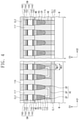
- FIG. 1 is a perspective view of an example of a variable resistance memory device according the inventive concepts.
- FIG. 2 is a circuit diagram of a memory cell stack of the variable resistance memory device of FIG. 1 .
- FIG. 3 is a plan view of examples of a variable resistance memory device according to the inventive concepts.
- FIG. 4 is a cross-sectional view of one example of a variable resistance memory device according to the inventive concepts taken along lines I-I′ and II-II′ of FIG. 3 .
- FIG. 5 is a cross-sectional view of another example of a variable resistance memory device according to the inventive concepts taken along the lines I-I′ and II-II′ of FIG. 3 .
- FIG. 6 is a flowchart of an example of a method of manufacturing a variable resistance memory device of FIG. 3 , according to the inventive concepts.
- FIGS. 7, 8, 9, 10, 11, 12, 13, 14 and 15 are cross-sectional views of a variable resistance memory device during the course of its manufacture, taken in directions corresponding to the directions of lines I-I′ and II-II′ of FIG. 3 .
- FIG. 16 is a flowchart of an example of an operation of forming a switching element in the method illustrated by the flowchart of FIG. 6 .
- FIG. 17 is a schematic diagram of a thin layer deposition apparatus for forming a lower barrier layer and an upper barrier layer in the stage of the method shown in FIG. 13 .
- FIG. 18 is a cross-sectional view of a conventional switching element.
- FIG. 19 is a cross-sectional view taken along the lines I-I′ and II-II′ of FIG. 3 .
- FIG. 20 is a cross-sectional view taken along the lines I-I′ and II-II′ of FIG. 3 .
- FIG. 21 is a perspective view of an example of a variable resistance memory device according to the inventive concepts.
- FIG. 22 is a perspective view of an example of a variable resistance memory device according to the inventive concepts.
- FIG. 23 is a plan view of examples of a variable resistance memory device according to the inventive concepts.
- FIG. 24 is a cross-sectional view taken along lines and IV-IV′ of FIG. 23 .
- FIG. 25 is a cross-sectional view taken along the lines and IV-IV′ of FIG. 23 .
- FIG. 26 is a perspective view of an example of a variable resistance memory device according to the inventive concepts.
- a variable resistance memory device 100 may include a plurality of memory cell arrays MCA sequentially stacked on a substrate W. Each of the memory cell arrays MCA may include a two-dimensional array of variable resistance memory cells.
- the variable resistance memory device 100 may further include conductive lines (not shown) which are disposed between the memory cell arrays and are used to write data to, read data from and/or erase the variable resistance memory cells.
- FIG. 1 illustrates a stack of five memory cell arrays MCA.
- the inventive concepts are not limited thereto.
- FIG. 2 is a circuit diagram of one of the memory cell arrays of FIG. 1 .
- a first memory cell array MCA 1 is illustrated as an example in FIG. 2 .
- the first memory cell array MCA 1 may include memory cells MC disposed at intersecting points, as viewed in plan, of first conductive lines CL 1 and second conductive lines CL 2 .
- a second memory cell array may be provided on the first memory cell array MCA 1 .
- the second memory cell array may include memory cells provided at intersecting points of third conductive lines and fourth conductive lines.
- the third conductive lines are separate conductive lines vertically spaced apart from the second conductive lines CL 2 .
- the second memory cell array may share the second conductive lines CL 2 with the first memory cell array MCA 1 .
- the third conductive lines correspond to the second conductive lines CL 2 .
- the memory cells MC of the first memory cell array MCA 1 may be two-dimensionally arrayed on the substrate W to constitute rows and columns.
- FIG. 3 is a plan view of the first and second conductive lines CL 1 and CL 2 and the memory cells MC represented in the circuit diagram of FIG. 2 .
- FIG. 4 is a cross-sectional view taken along lines I-I′ and II-II′ of FIG. 3 .
- FIGS. 2, 3 and 4 may together illustrate an example of a variable resistance memory device according to the inventive concepts.
- the first conductive lines CL 1 may extend in a first direction D 1 on the substrate W
- the second conductive lines CL 2 may extend in a second direction D 2 on the substrate W.
- the substrate W may include a single-crystalline semiconductor material.
- the substrate W may be a silicon substrate, a silicon-on-insulator (SOI) substrate, a germanium substrate, a germanium-on-insulator (GOI) substrate or a silicon-germanium (SiGe) substrate.
- the first conductive lines CL 1 may be word lines
- the second conductive lines CL 2 may be bit lines.
- the first conductive lines CL 1 may be bit lines
- the second conductive lines CL 2 may be word lines.
- the first and second conductive lines CL 1 and CL 2 include a conductive material such as copper or aluminum.
- the first and second conductive lines CL 1 and CL 2 may further include a conductive metal nitride such as TiN or WN.
- the first conductive lines CL 1 may be provided in a lower insulating layer 105 .
- the second conductive lines CL 2 may be provided in an upper insulating layer 119 .
- the lower insulating layer 105 and the upper insulating layer 119 may each be a silicon oxide or silicon oxynitride layer.
- each of the memory cells MC includes a variable resistor and a switch, respectively referred to hereinafter as variable resistance structure CR and a switching element SW.
- the variable resistance structure CR may be connected to the first conductive line CL 1 .
- the variable resistance structure CR has a resistance value which is variable to store logic data.
- the switching element SW may be connected to the second conductive line CL 2 .
- the switching element SW may connect the second conductive line CL 2 to the variable resistance structure CR when a voltage higher than a threshold voltage (V th ) of the switching element SW is impressed across the switching element, i.e., the switching element SW selectively electrically conductively connects the variable resistance structure CR to the second conductive line CL 2 .
- the memory cell MC may further include an intermediate electrode ME between the variable resistance structure CR and the switching element SW.
- the variable resistance structure CR may be provided between the switching element SW and the substrate W. Alternatively, the switching element SW is provided between the variable resistance structure CR and the substrate W.
- V th threshold voltage
- the variable resistance structure CR may be provided in a recess RS formed in first to third interlayer insulating layers 111 , 113 and 115 on the first conductive line CL 1 .
- the first to third interlayer insulating layers 111 , 113 and 115 may each be a silicon nitride or silicon oxynitride layer.
- a plurality of the recesses RS may be respectively disposed at intersecting points of the first conductive lines CL 1 and the second conductive lines CL 2 and may be two-dimensionally arranged, when viewed in a plan view.
- the variable resistance structure CR may have a line shape extending in the first direction D 1 or the second direction D 2 .
- the variable resistance structure CR may be formed of at least one material capable of storing logical data.
- the variable resistance structure CR includes a material having a phase transition temperature across which its phase changes between a crystalline phase and an amorphous phase.
- a phase transition temperature between the crystalline and amorphous phases of the variable resistance structure CR may range from about 250 degrees Celsius to about 350 degrees Celsius.
- the variable resistance structure CR may be formed of a compound that includes at least one of Te and Se (i.e., chalcogenide elements) and at least one material selected from the group consisting of Ge, Sb, Bi, Pb, Sn, Ag, As, S, Si, In, Ti, Ga, P, O, and C.
- variable resistance structure CR may include a layer (pattern) of GeSbTe, GeTeAs, SbTeSe, GeTe, SbTe, SeTeSn, GeTeSe, SbSeBi, GeBiTe, GeTeTi, InSe, GaTeSe or InSbTe.
- variable resistance structure CR may include at least one of a binary compound (e.g., GeTe, GeSe, GeS, SbSe, SbTe, SbS, SbSe, SnSb, InSe, InSb, AsTe, AlTe, GaSb, AlSb, BiSb, ScSb, Ysb, CeSb, DySb, or NdSb), a ternary compound (e.g., GeSbSe, AlSbTe, AlSbSe, SiSbSe, SiSbTe, GeSeTe, InGeTe, GeSbTe, GeAsTe, SnSeTe, GeGaSe, BiSbSe, GaSeTe, InGeSb, GaSbSe, GaSbTe, InSbSe, InSbTe, SnSbSe, SnSbTe, ScSbTe, ScSbTe,
- variable resistance structure CR may have a superlattice structure in which layers including Ge and layers not including Ge are repeatedly and alternately stacked.
- the variable resistance structure CR may have a structure in which GeTe layers and SbTe layers are repeatedly and alternately stacked.
- the variable resistance structure CR may include at least one of B, C, N, O, P, Ca, W, Ti, Hf, or Zr.
- variable resistance structure CR includes at least one material selected from the group of perovskite compounds and the group of conductive metal oxides.
- the variable resistance structure CR may include a layer (pattern) of niobium oxide, titanium oxide, nickel oxide, zirconium oxide, vanadium oxide, (Pr,Ca)MnO 3 (PCMO), strontium-titanium oxide, barium-strontium-titanium oxide, strontium-zirconium oxide, barium-zirconium oxide, or barium-strontium-zirconium oxide.
- PCMO niobium oxide
- PCMO PCMO
- strontium-titanium oxide barium-strontium-titanium oxide
- strontium-zirconium oxide strontium-zirconium oxide
- barium-zirconium oxide barium-zirconium oxide
- barium-strontium-zirconium oxide barium-strontium-zirconium oxide.
- variable resistance structure CR has a double-layer structure of a conductive metal oxide layer and a tunnel insulating layer. In certain other examples, the variable resistance structure CR has a triple-layer structure of a first conductive metal oxide layer, a tunnel insulating layer and a second conductive metal oxide layer.
- the tunnel insulating layer may include aluminum oxide, hafnium oxide, or silicon oxide.
- a heater electrode HE may be provided between the first conductive line CL 1 and the variable resistance structure CR.
- the heater electrode HE may connect respective ones of the variable resistance structures CR, adjacent to each other in the first direction D 1 , to the first conductive line CL 1 .
- the heater electrode HE may include a horizontal portion BP connected to the first conductive line CL 1 , and a pair of vertical portions SP extending from ends of the horizontal portion BP to the variable resistance structures CR, respectively.
- a plurality of the heater electrodes HE may be respectively disposed at the intersecting points of the first conductive lines CL 1 and the second conductive lines CL 2 and may be two-dimensionally arranged.
- the heater electrode HE serves to heat the variable resistance structure CR to change the phase of the variable resistance structure CR.
- the heater electrode HE may be formed of a material whose resistivity is greater than that of the first conductive line CL 1 .
- the heater electrode HE may include at least one layer (pattern) of material selected from the group consisting of W, Ti, Al, Cu, C, CN, TiN, TiAlN, TiSiN, TiCN, WN, CoSiN, WSiN, TaN, TaCN, TaSiN, or TiO.
- a spacer pattern 120 may be provided between the heater electrode HE and the second interlayer insulating layer 113 .
- the spacer pattern 120 may extend along the horizontal portion BP and the vertical portions SP of the heater electrode HE.
- the spacer pattern 120 may be formed of silicon oxide and/or silicon oxynitride.
- a lower portion of the recess RS may be occupied by the variable resistance structure CR, and an upper portion of the recess RS may be occupied by the intermediate electrode ME.
- the intermediate electrode ME electrically connects the variable resistance structure CR and the switching element SW and prevents the variable resistance structure CR from being in direct contact with the switching element SW.
- the intermediate electrode ME may include at least one layer (pattern) of material selected from the group consisting of W, Ti, Al, Cu, C, CN, TiN, TiAlN, TiSiN, TiCN, WN, CoSiN, WSiN, TaN, TaCN, and TaSiN.
- Top surfaces of the first to third interlayer insulating layers 111 , 113 and 115 may be substantially coplanar with a top surface of the intermediate electrode ME.
- the intermediate electrode ME may be provided on the first to third interlayer insulating layers 111 , 113 and 115 .
- the switching element SW may be disposed on the intermediate electrode ME.
- the switching element SW includes an ovonic threshold switch (OTS) element having a bi-directional characteristic.
- OTS ovonic threshold switch
- the switching element SW may include an element based on a threshold switching phenomenon having a nonlinear I-V curve (e.g., a S-shaped I-V curve).
- the switching element SW includes a switching pattern 130 , a lower barrier electrode 140 , an upper barrier electrode 150 , and an upper electrode 160 .
- the switching pattern 130 may be disposed on the lower barrier electrode 140 .
- the switching pattern 130 may have a phase transition temperature between crystalline and amorphous phases, which is higher than that of the variable resistance structure CR.
- the phase transition temperature of the switching pattern 130 may range from about 350 degrees Celsius to about 450 degrees Celsius.
- an operating voltage e.g., a program voltage
- a substantially amorphous state of the switching pattern 130 may be maintained without phase change even though the operating voltage is applied thereto.
- the switching pattern 130 may be formed of a compound that includes at least one of Te and Se (i.e., at least one chalcogenide element) and at least one material selected from the group consisting of Ge, Sb, Bi, Al, Pb, Sn, Ag, As, S, Si, In, Ti, Ga, and P.
- the switching pattern 130 may further include a thermal stabilization element in addition to the compound.
- the thermal stabilization element may include at least one of C, N, and O.
- the switching pattern 130 may include at least one of a binary compound (e.g., GeSe, GeS, AsSe, AsTe, AsS SiTe, SiSe, SiS, GeAs, SiAs, SnSe, or SnTe), a ternary compound (e.g., GeAsTe, GeAsSe, AlAsTe, AlAsSe, SiAsSe, SiAsTe, GeSeTe, GeSeSb, GaAsSe, GaAsTe, InAsSe, InAsTe, SnAsSe, or SnAsTe), a quaternary compound (e.g., GeSiAsTe, GeSiAsSe, GeSiSeTe, GeSeTeSb, GeSiSeSb, GeSiTeSb, GeSeTeBi, GeSiSeBi, GeSiTeBi, GeSi
- the switching pattern 130 may include a single layer including one of the materials described above.
- the switching pattern 130 may include a plurality of layers, and the plurality of layers may include different materials of the materials described above.
- the switching pattern 130 may further include at least one of B, C, N, or O.
- the lower barrier electrode 140 may be disposed between the intermediate electrode ME and the switching pattern 130 .
- the lower barrier electrode 140 may prevent or minimize heat transfer between the intermediate electrode ME and the switching pattern 130 .
- the lower barrier electrode 140 is a multi-layered structure of electrode layers distinguished from each by a difference in their respective densities, and may also have different resistivities and/or surface roughnesses.
- the lower barrier electrode 140 includes a first layer of barrier material and a second layer of barrier material respectively referred to hereinafter as a first lower barrier electrode 142 (or first lower barrier electrode layer) and a second lower barrier electrode 144 (or second lower barrier electrode layer).
- the term “layer” especially when specifically used will be generally understood as referring to a monolayer, i.e., a generally homogeneous layer of material.
- the first lower barrier electrode 142 may be disposed between the intermediate electrode ME and the switching pattern 130 .
- the first lower barrier electrode 142 may reduce stress between the intermediate electrode ME and the switching pattern 130 and may increase adhesive strength therebetween.
- the first lower barrier electrode 142 is wider than the intermediate electrode ME in the first direction D 1 or the second direction D 2 .
- the intermediate electrode ME may have a first width WD 1
- the first lower barrier electrode 142 may have a second width WD 2 greater than the first width WD 1 .
- the first lower barrier electrode 142 may also be disposed between the switching pattern 130 and a portion of the first to third interlayer insulating layers 111 , 113 and 115 .
- the first lower barrier electrode 142 may reduce stress between the switching pattern 130 and the portion of the first to third interlayer insulating layers 111 , 113 and 115 and may increase adhesive strength therebetween.
- the first lower barrier electrode 142 is or includes low-density carbon film having a density less than about 2.0 g/cm 3 , e.g., a density of about 1.73 g/cm 3 .
- the first lower barrier electrode 142 may have a resistivity of about 46.5 m ⁇ cm and a surface roughness of about 1.0 nm.
- the first lower barrier electrode 142 may further include an inert gas element (e.g., Ar) of about 1 at % or less.
- the first lower barrier electrode 142 may further include carbon nitride.
- the second lower barrier electrode 144 may be disposed between the first lower barrier electrode 142 and the switching pattern 130 .
- the density of the second lower barrier electrode 144 may be higher than the density of the first lower barrier electrode 142 .
- the second lower barrier electrode 144 may include high-density carbon film having a density greater than about 2.0 g/cm 3 , e.g. a density of about 2.34 g/cm 3 .
- the term “about” encompasses not only the specification for the density of the material but slight variations therefrom arising from inherent aspects of the process used to form the material to its specifications.
- the second lower barrier electrode 144 may minimize or prevent diffusion of elements included in the switching pattern 130 . In addition, the second lower barrier electrode 144 may minimize or prevent intermixing of the first lower barrier electrode 142 and the switching pattern 130 .
- a resistivity of the second lower barrier electrode 144 may be less than the resistivity of the first lower barrier electrode 142 .
- a surface roughness of the second lower barrier electrode 144 may be less than the surface roughness of the first lower barrier electrode 142 .
- the second lower barrier electrode 144 may have a resistivity of about 24.8 m ⁇ cm and a surface roughness of about 0.4 nm.
- the second lower barrier electrode 144 may include a larger amount of an inert gas element than the first lower barrier electrode 142 .
- the second lower barrier electrode 144 may further include the inert gas element (e.g., Ar) of about 4 at % or more. The inert gas element may be provided into the second lower barrier electrode 144 through a densification process.
- the upper barrier electrode 150 may be disposed on the switching pattern 130 .
- the upper barrier electrode 150 may minimize or prevent heat transfer between the switching pattern 130 and the second conductive line CL 2 .
- the upper barrier electrode 150 may be a multi-layered structure including electrode layers distinguished from each other by differences in their respective densities, and may also be distinguished from each other by differences in their resistivities and/or surface roughnesses.
- the upper barrier electrode 150 may include a smaller amount of an inert gas element (e.g., Ar) than the lower barrier electrode 140 .
- the upper barrier electrode 150 may include a larger amount of the inert gas element than the lower barrier electrode 140 .
- the upper barrier electrode 150 includes a first upper barrier electrode 152 and a second upper barrier electrode 154 .
- the first upper barrier electrode 152 may be disposed between the switching pattern 130 and the second upper barrier electrode 154 .
- the first upper barrier electrode 152 may have a density of about 2.34 g/cm 3 .
- the first upper barrier electrode 152 may be a high-density carbon film.
- the first upper barrier electrode 152 may minimize or prevent diffusion of the elements included in the switching pattern 130 .
- the first upper barrier electrode 152 may minimize or prevent intermixing of the switching pattern 130 and the second upper barrier electrode 154 .
- the first upper barrier electrode 152 may have a resistivity of about 24.8 m ⁇ cm and a surface roughness of about 0.4 nm.
- the first upper barrier electrode 152 may further include the inert gas element (e.g., Ar) of about 1 at % or less. The inert gas element may be provided into the first upper barrier electrode 152 through a densification process.
- the inert gas element e.g., Ar
- the second upper barrier electrode 154 may be disposed between the first upper barrier electrode 152 and the upper electrode 160 .
- the density of the second upper barrier electrode 154 may be less than the density of the first upper barrier electrode 152 .
- the second upper barrier electrode 154 may have a density of about 1.73 g/cm 3 .
- the second upper barrier electrode 154 may be a low-density carbon film.
- the second upper barrier electrode 154 may reduce stress between the first upper barrier electrode 152 and the upper electrode 160 and may increase adhesive strength therebetween.
- the second upper barrier electrode 154 may have a resistivity of about 46.5 m ⁇ cm and a surface roughness of about 1.0 nm.
- the second upper barrier electrode 154 may further include a larger amount of the inert gas element than the first upper barrier electrode 152 .
- the second upper barrier electrode 154 may include the inert gas element (e.g., Ar) of about 4 at % or more.
- the upper electrode 160 may be disposed on the second upper barrier electrode 154 .
- the upper electrode 160 may electrically connect the second conductive line CL 2 to the switching pattern 130 .
- the upper electrode 160 may include at least one of W, Ti, Al, Cu, C, CN, TiN, TiAlN, TiSiN, TiCN, WN, CoSiN, WSiN, TaN, TaCN, TaSiN, and TiO.
- a fourth interlayer insulating layer 117 may fill the space between the upper electrodes 160 .
- the fourth interlayer insulating layer 117 may be disposed between the upper insulating layer 119 and the first to third interlayer insulating layers 111 , 113 and 115 .
- a top surface of the fourth interlayer insulating layer 117 may be substantially coplanar with a top surface of the upper electrode 160 .
- the fourth interlayer insulating layer 117 may include at least one of silicon oxide, silicon nitride, silicon oxynitride, silicon oxycarbide, silicon oxycarbonitride, and silicon carbonitride.
- the upper insulating layer 119 and the second conductive line CL 2 may be provided on the fourth interlayer insulating layer 117 .
- FIG. 5 is a cross-sectional view taken along lines I-I′ and II-II′ of FIG. 3 and together with FIG. 2 illustrate another example of a variable resistance memory device according to the inventive concepts.
- FIG. 5 is a cross-sectional view taken along lines I-I′ and II-II′ of FIG. 3 and together with FIG. 2 illustrate another example of a variable resistance memory device according to the inventive concepts.
- the density of the second upper barrier electrode layer 154 may be higher than the density of the first upper barrier electrode layer 152 .
- a surface roughness of the second upper barrier electrode layer 154 may be less than a surface roughness of the first upper barrier electrode layer 152 .
- the first upper barrier electrode layer 152 may be a layer of low-density carbon, and the second upper barrier electrode 154 may be a layer of high-density carbon.
- FIG. 6 is a flowchart illustrating a method of manufacturing the variable resistance memory device 100 of FIG. 3 .
- a method of manufacturing the variable resistance memory device 100 may include forming a first conductive line CL 1 (S 100 ), forming a heater electrode HE (S 200 ), forming a variable resistance structure CR and an intermediate electrode ME (S 300 ), forming a switching element SW (S 400 ), and forming a second conductive line CL 2 (S 500 ).
- FIGS. 7 to 15 are cross-sectional views taken in the direction of lines I-I′ and II-II′ of FIG. 3 to illustrate an example of the method of manufacturing the variable resistance memory device of FIG. 3 .
- the first conductive line CL 1 are formed on a substrate W (S 100 ).
- the first conductive lines CL 1 are formed by a deposition process of forming a metal layer, a photolithography process, and an etching process. Thereafter, a lower insulating layer 105 is formed between the first conductive lines CL 1 .
- the first conductive lines CL 1 are formed by a damascene method.
- the lower insulating layer 105 having lower trenches may be formed on the substrate W, and then, the first conductive lines CL 1 may be formed in the lower trenches by a deposition process of forming a blanket metal layer filling the lower trench and a chemical mechanical polishing (CMP) process of planarizing the metal layer.
- CMP chemical mechanical polishing
- the heater electrodes HE are formed on the first conductive lines CL 1 (S 200 ).
- the forming of the heater electrodes HE includes forming the first to third interlayer insulating layers 111 , 113 and 115 .
- FIG. 8 an example of forming a heater electrode HE on one of the first conductive lines CL 1 will be described. Note, too, in the description that follows, the forming of only one element or feature may be described at times for simplicity although the method may entail the forming of multiple ones of the elements or features at once as will be clear from the figures.
- the first interlayer insulating layer 111 may be formed on the first conductive line CL 1 and the lower insulating layer 105 .
- the first interlayer insulating layer 111 may be formed of silicon nitride or silicon oxynitride.
- An upper trench TC may be formed in the first interlayer insulating layer 111 .
- the forming of the upper trench TC may include an anisotropic etching process.
- the upper trench TC may intersect the first conductive line CL 1 .
- an electrode layer 121 and a spacer layer 126 may be sequentially formed on the first interlayer insulating layer 111 having the upper trench TC.
- the electrode layer 121 and the spacer layer 126 may be conformally formed along surfaces defining the upper trench TC.
- the electrode layer 121 may include a layer of W, Ti, Al, Cu, C, CN, TiN, TiAlN, TiSiN, TiCN, WN, CoSiN, WSiN, TaN, TaCN, TaSiN, or TiO.
- the spacer layer 126 may include at least one of silicon oxide and silicon oxynitride.
- the second interlayer insulating layer 113 may be formed on the spacer layer 126 to fill the remainder of the upper trench TC.
- the second interlayer insulating layer 113 may be formed of the same material as the first interlayer insulating layer 111 .
- the second interlayer insulating layer 113 , the spacer layer 126 , and the electrode layer 121 may be planarized until the first interlayer insulating layer 111 is exposed. Subsequently, portions of the first and second interlayer insulating layers 111 and 113 , the spacer layer 126 and the electrode layer 121 , which do not overlap the first conductive line CL 1 , may be etched to form an opening OP. As a result, the heater electrode HE may be formed from the electrode layer 121 and a spacer pattern 120 may be formed from the spacer layer 126 .
- a plurality of the heater electrodes HE may be formed and may be spaced apart from each other in the first direction D 1 and the second direction D 2 . Thereafter, the third interlayer insulating layer 115 may be formed to fill the opening OP.
- the third interlayer insulating layer 115 may be formed of the same material as the first interlayer insulating layer 111 .
- the forming of the third interlayer insulating layer 115 may include a deposition process of forming a dielectric and a CMP process.
- variable resistance structure CR and the intermediate electrode ME may be formed on the heater electrode HE (S 300 ).
- the variable resistance structure CR and the intermediate electrode ME may be formed by a damascene method.
- a recess RS may be formed to expose the heater electrode HE.
- the forming of the recess RS may include a process of etching an upper portion of the spacer pattern 120 and a process of etching an upper portion of the heater electrode HE.
- Each of the processes of etching the spacer pattern 120 and the heater electrode HE may be a wet etching process.
- an isotropic wet etching process may be performed to expand the space formed by etching the upper portion of the heater electrode HE and the upper portion of the spacer pattern 120 .
- the isotropic wet etching process may be performed using an etchant including phosphoric acid.
- variable resistance structure CR is formed in the recess RS.
- a variable resistance layer is formed to fill the recess RS, and then, an upper portion of the variable resistance layer is etched to form the variable resistance structure CR.
- variable resistance layer may include at least one of a binary compound (e.g., GeTe, GeSe, GeS, SbSe, SbTe, SbS, SbSe, SnSb, InSe, InSb, AsTe, AlTe, GaSb, AlSb, BiSb, ScSb, Ysb, CeSb, DySb, or NdSb), a ternary compound (e.g., GeSbSe, AlSbTe, AlSbSe, SiSbSe, SiSbTe, GeSeTe, InGeTe, GeSbTe, GeAsTe, SnSeTe, GeGaSe, BiSbSe, GaSeTe, InGeSb, GaSbSe, GaSbTe, InSbSe, InSbTe, SnSbSe, SnSbTe, ScSbTe, ScSbSe, ScS
- variable resistance layer may be formed by a physical vapor deposition (PVD) method or a chemical vapor deposition (CVD) method.
- the variable resistance layer may further include impurities including at least one of B, C, N, O, P, Ca, W, Ti, Hf, or Zr.
- an intermediate electrode ME is formed in an upper portion of the recess RS.
- the intermediate electrode ME may be formed of at least one layer of material selected from the group consisting of W, Ti, Al, Cu, C, CN, TiN, TiAlN, TiSiN, TiCN, WN, CoSiN, WSiN, TaN, TaCN, and TaSiN.
- an electrode layer(s) is formed on the resultant structure having the variable resistance structure CR, and then, the electrode layer(s) is planarized to form the intermediate electrode ME.
- the process of forming the intermediate electrode ME may be omitted.
- the switching element SW is formed on the resultant structure, e.g., the structure having the intermediate electrode ME (S 400 ).
- the switching element SW may be formed by a thin layer deposition process, a photolithography process, and an etching process.
- FIG. 16 is a flowchart illustrating an example of the operation S 400 of forming the switching element SW in the method of FIG. 6 .
- an example of the operation S 400 of forming the switching element SW includes forming a lower barrier layer 141 (S 410 ), depositing a switching layer 132 (S 420 ), forming an upper barrier layer 151 (S 430 ), depositing an upper electrode layer 162 (S 440 ), and etching portions of the lower barrier layer 141 , the switching layer 132 , the upper barrier layer 151 and the upper electrode layer 162 .
- FIG. 17 illustrates a thin layer deposition apparatus 1000 for forming the lower barrier layer 141 and the upper barrier layer 151 of FIG. 13 .
- the thin layer deposition apparatus 1000 is a sputtering apparatus.
- the thin layer deposition apparatus 1000 may include a chamber 1 , a heater chuck 2 , a target 3 , a magnetron 4 , first and second power supply units 6 and 7 , and a gas supply unit 8 .
- the gas supply unit 8 provides a process gas into the chamber 1 .
- the process gas may include argon (Ar), nitrogen (N 2 ), or krypton (Kr).
- the heater chuck 2 may be disposed in a lower portion of the chamber 1
- the magnetron 4 may be disposed in an upper portion of the chamber 1 .
- the substrate W may be provided on the heater chuck 2 .
- the target 3 may be fixed on a bottom surface of the magnetron 4 .
- the target 3 may include a carbon target, a compound target, or a metal target.
- the compound target may include a compound that includes at least one of Te and Se (i.e., one or more chalcogenide elements) and at least one material selected from the group consisting of Ge, Sb, Bi, Al, Pb, Sn, Ag, As, S, Si, In, Ti, Ga, and P.
- the metal target may include titanium or titanium nitride.
- the first power supply unit 6 may provide first radio-frequency power 5 (e.g., source power) to the magnetron 4 .
- the first radio-frequency power 5 excites the process gas to induce plasma in the chamber 1 .
- the first radio-frequency power 5 may accelerate the plasma toward the target 3 to generate target particles.
- the target particles may be deposited as a thin layer on the substrate W.
- the second power supply unit 7 may provide second radio-frequency power 9 (e.g., bias power) to the heater chuck 2 .
- the second radio-frequency power 9 may accelerate the target particles and the plasma toward the substrate W to increase the density of the thin layer.
- the thin layer deposition apparatus 1000 may form the lower barrier layer 141 by using the target 3 which is the carbon target (S 410 ).
- the lower barrier layer 141 may be formed by a sputtering method.
- the lower barrier layer 141 is formed by forming a first lower barrier layer 143 (S 412 ) and forming a second lower barrier layer 145 (S 414 ).
- the first power supply unit 6 may supply the first radio-frequency power 5 to the magnetron 4 to form the first lower barrier layer 143 on the substrate W (S 412 ).
- the heater chuck 2 may heat the substrate W to a high temperature of about 350 degrees Celsius.
- the gas supply unit 8 may provide the argon gas as the process gas over the substrate W.
- the first lower barrier layer 143 may include low-density carbon.
- the first lower barrier layer 143 may further include an inert gas element (e.g., Ar) of about 1 at % or less.
- the first lower barrier layer 143 may further include carbon nitride.
- the first and second power supply units 6 and 7 may supply the first and second radio-frequency powers 5 and 9 to the magnetron 4 and the heater chuck 2 , respectively, to form the second lower barrier layer 145 on the substrate W (S 414 ).
- the heater chuck 2 may heat the substrate W to a low temperature of about 150 degrees Celsius.
- the gas supply unit 8 may provide the nitrogen gas or the krypton gas as the process gas over the substrate W.
- the second lower barrier layer 145 is formed on the first lower barrier layer 143 .
- the second lower barrier layer 145 may be formed to be denser than the first lower barrier layer 143 , through a densification process.
- the second lower barrier layer 145 may include high-density carbon.
- the second lower barrier layer 145 includes high-density carbon doped with nitrogen (N).
- the second lower barrier layer 145 may include an inert gas element (e.g., Ar) of about 4 at % or more.
- the switching layer 132 may be formed by a sputtering method (S 420 ).
- the switching layer 132 may be formed of a compound that includes at least one of Te or Se (i.e., one or more chalcogenide elements) and at least one material selected from the group consisting of Ge, Sb, Bi, Al, Pb, Sn, Ag, As, S, Si, In, Ti, Ga, and P.
- the switching layer 132 may further include a thermal stabilization element in addition to the compound.
- the thermal stabilization element may include at least one of B, C, N, or O.
- the switching layer 132 may include at least one of a binary compound (e.g., GeSe, GeS, AsSe, AsTe, AsS, SiTe, SiSe, SiS, GeAs, SiAs, SnSe, or SnTe), a ternary compound (e.g., GeAsTe, GeAsSe, AlAsTe, AlAsSe, SiAsSe, SiAsTe, GeSeTe, GeSeSb, GaAsSe, GaAsTe, InAsSe, InAsTe, SnAsSe, or SnAsTe), a quaternary compound (e.g., GeSiAsTe, GeSiAsSe, GeSiSeTe, GeSeTeSb, GeSiSeSb, GeSiTeSb, GeSeTeBi, GeSiSeBi, GeSiTeBi, Ge
- the thin layer deposition apparatus 1000 may form the upper barrier layer 151 by using the target 3 which is the carbon target (S 430 ).
- the upper barrier layer 151 may be formed by a sputtering method.
- the upper barrier layer 151 is formed by forming a first upper barrier layer 153 (S 432 ) and forming a second upper barrier layer 155 (S 434 ).
- the first and second power supply units 6 and 7 may supply the first and second radio-frequency powers 5 and 9 to the magnetron 4 and the heater chuck 2 , respectively, to form the first upper barrier layer 153 on the substrate W (S 432 ).
- the heater chuck 2 may heat the substrate W to a low temperature of about 150 degrees Celsius.
- the gas supply unit 8 may provide the nitrogen gas or the krypton gas as the process gas over the substrate W.
- the first upper barrier layer 153 may include high-density carbon.
- the first upper barrier layer 153 includes high-density carbon doped with nitrogen (N).
- the first power supply unit 6 may supply the first radio-frequency power 5 to the magnetron 4 to form the second upper barrier layer 155 on the substrate W (S 434 ).
- the heater chuck 2 may heat the substrate W to a high temperature of about 350 degrees Celsius.
- the gas supply unit 8 may provide the argon gas as the process gas over the substrate W.
- the second upper barrier layer 155 may include low-density carbon.
- the upper electrode layer 162 may be formed by a sputtering method (S 440 ).
- the upper electrode layer 162 may include at least one material slected from the group consisting of W, Ti, Al, Cu, C, CN, TiN, TiAlN, TiSiN, TiCN, WN, CoSiN, WSiN, TaN, TaCN, TaSiN, and TiO.
- an etching apparatus may etch the portions of the lower barrier layer 141 , the switching layer 132 , the upper barrier layer 151 and the upper electrode layer 162 to form the switching element SW (S 450 ).
- the portions of the lower barrier layer 141 , the switching layer 132 , the upper barrier layer 151 and the upper electrode layer 162 may be etched by a reactive ion etching (RIE) method.
- the switching element SW may include a lower barrier electrode 140 , a switching pattern 130 , an upper barrier electrode 150 , and an upper electrode 160 .
- the upper barrier electrode 150 may include first and second upper barrier electrodes 152 and 154 , and the first and second upper barrier electrodes 152 and 154 may be formed from the first and second upper barrier layers 153 and 155 , respectively.
- the lower barrier electrode 140 may include first and second lower barrier electrodes 142 and 144 , and the first and second lower barrier electrodes 142 and 144 may be formed from the first and second lower barrier layers 143 and 145 , respectively.
- the first lower barrier layer 143 may increase adhesive strength of the switching element SW with respect to the intermediate electrode ME and/or the first to third interlayer insulating layers 111 , 113 and 115 .
- the first lower barrier layer 143 may minimize or prevent a leaning phenomenon and/or a detachment phenomenon of the switching element SW during the etching process for forming the switching element SW.
- FIG. 18 illustrates examples of a conventional switching element 190 formed using an etching process.
- a typical switching element 190 includes a first barrier electrode 192 and a second barrier electrode 194 .
- the first barrier electrode 192 is interposed between a substrate W and a switching pattern 130 .
- the first barrier electrode 192 includes high-density carbon.
- the first barrier electrode 192 reduces or weakens adhesive strength between the substrate W and the switching pattern 130 in an etching process, and thus the conventional switching element 190 may lean and/or be detached.
- the conventional switching element 190 may even separate from the substrate W.
- the second barrier electrode 194 is interposed between the switching pattern 130 and an upper electrode 160 .
- the second barrier electrode 194 includes high-density carbon.
- the second barrier electrode 194 reduces adhesive strength between the switching pattern 130 and the upper electrode 160 in an etching process to cause detachment of the upper electrode 160 .
- the upper electrode 160 may separate from the second barrier electrode 194 .
- the upper barrier electrode 150 of a switching element includes the first and second upper barrier electrodes 152 and 154 formed from the first and second upper barrier layers 153 and 155 , respectively.
- the second upper barrier electrode 154 provides a high degree of adhesive strength between the first upper barrier electrode 152 and the upper electrode 160 during the etching process of forming the first and second upper barrier layers 153 and 155 .
- detachment of the upper electrode 160 may be minimized or prevented.
- the upper electrode 160 may be formed from the upper electrode layer 162 through the etching process.
- a fourth interlayer insulating layer 117 may be formed between the switching elements SW.
- the fourth interlayer insulating layer 117 may be formed by a deposition process of a dielectric and a CMP process performed on the deposited dielectric.
- the second conductive line CL 2 may be formed on a portion of the fourth interlayer insulating layer 117 and the switching element SW (S 500 ).
- the second conductive line CL 2 may be formed by a deposition process of forming a metal layer, a photolithography process, and an etching process.
- an upper insulating layer 119 may be formed between the second conductive lines CL 2 .
- the upper insulating layer 119 may be formed by a process of deposition a dielectric and a CMP process performed on the deposited dielectric.
- FIG. 19 is a cross-sectional view taken along the lines I-I′ and II-II′ of FIG. 3 .
- a variable resistance memory device 100 may include a cross-point PRAM array or a three-dimensional (3D) memory array.
- a switching element SW may be disposed under a variable resistance structure CR.
- the switching element SW may be disposed on the variable resistance structure CR.
- embodiments of the inventive concepts are not limited thereto.
- An interlayer insulating layer 110 may be provided between a substrate W and first conductive lines CL 1 .
- the interlayer insulating layer 110 may include at least one of a silicon oxide layer, a silicon nitride layer, or a silicon oxynitride layer.
- Lower filling structures GS 0 may fill spaces between the first conductive lines CL 1 and may extend in the first direction D 1 along the first conductive lines CL 1 .
- Each of the lower filling structures GS 0 may have a bar or line shape extending in the first direction D 1 when viewed in a plan view.
- the lower filling structures GS 0 may include at least one of silicon oxide, silicon nitride, or silicon oxynitride.
- the lower filling structures GS 0 may extend into an upper portion of the interlayer insulating layer 110 . In other words, lower portions of the lower filling structures GS 0 may be inserted in the upper portion of the interlayer insulating layer 110 .
- a lower barrier electrode 140 may be disposed between the first conductive line CL 1 and a switching pattern 130 .
- the lower barrier electrode 140 may include a first lower barrier electrode 142 and a second lower barrier electrode 144 .
- the first lower barrier electrode 142 may include carbon nitride.
- the second lower barrier electrode 144 may be disposed on the first lower barrier electrode 142 .
- the second lower barrier electrode 144 may include carbon.
- a density of the second lower barrier electrode 144 may be greater than a density of the first lower barrier electrode 142 .
- the second lower barrier electrode 144 may contain a larger amount of an inert gas element (e.g., Ar) than the first lower barrier electrode 142 .
- the first lower barrier electrode 142 may include the inert gas element of about 1 at % or less.
- the second lower barrier electrode 144 may include the inert gas element of about 4 at % or more.
- the switching pattern 130 may be disposed between the second lower barrier electrode 144 and the variable resistance structure CR.
- a first metal pattern MB 1 may be provided between the switching element SW and the variable resistance structure CR.
- An upper barrier electrode 150 may be disposed between the switching pattern 130 and the first metal pattern MB 1 .
- the upper barrier electrode 150 may include a first upper barrier electrode 152 and a second upper barrier electrode 154 .
- the first upper barrier electrode 152 may include carbon.
- the second upper barrier electrode 154 may be disposed on the first upper barrier electrode 152 .
- a density of the second upper barrier electrode 154 may be greater than a density of the first upper barrier electrode 152 .
- the second upper barrier electrode 154 may include high-density carbon
- the first upper barrier electrode 152 may include low-density carbon.
- the density of the first upper barrier electrode 152 may be about 1.73 g/cm 3
- the density of the second upper barrier electrode 154 may be about 2.34 g/cm 3 .
- the first upper barrier electrode 152 may include carbon
- the second upper barrier electrode 154 may include carbon nitride.
- the second upper barrier electrode 154 may be formed through a densification process.
- the second upper barrier electrode 154 may contain a larger amount of an inert gas element (e.g., Ar) than the first upper barrier electrode 152 .
- the first upper barrier electrode 152 may include the inert gas element of about 1 at % or less.
- the second upper barrier electrode 154 may include the inert gas element of about 4 at % or more.
- Heater electrodes HE may be provided between the variable resistance structures CR and second conductive lines CL 2 .
- a second metal pattern MB 2 may be provided between the heater electrode HE and the variable resistance structure CR.
- the variable resistance structure CR may be disposed between the first metal pattern MB 1 and the second metal pattern MB 2 .
- the variable resistance structure CR may have recess portions on its sidewalls.
- the recess portion may be a region in which the sidewall of the variable resistance structure CR is recessed from a sidewall of the first metal pattern MB 1 and a sidewall of the second metal pattern MB 2 .
- the first metal pattern MB 1 and the second metal pattern MB 2 may cover a bottom surface and a top surface of the variable resistance structure CR to prevent diffusion of the material of the variable resistance structure CR.
- the first metal pattern MB 1 may be provided between the variable resistance structure CR and the switching element SW to reduce a contact resistance therebetween.
- the first and second metal patterns MB 1 and MB 2 may include at least one of W, Ti, Al, Cu, C, CN, TiN, TiAlN, TiSiN, TiCN, WN, CoSiN, WSiN, TaN, TaCN, or TaSiN.
- a first memory cell MC 1 may further include a spacer structure SS.
- the spacer structure SS may cover the sidewalls of the first metal pattern MB 1 , the second metal pattern MB 2 , the variable resistance structure CR and the heater electrode HE.
- a bottom surface of the spacer structure SS may be in contact with a top surface of the upper barrier electrode 150 .
- the spacer structure SS may include at least one of a silicon oxide layer, a silicon nitride layer, or a silicon oxynitride layer.
- the spacer structure SS may include a first spacer ST 1 and a second spacer ST 2 which include different materials.
- the first spacer ST 1 may fill the recess portions of the variable resistance structure CR.
- the second spacer ST 2 may cover a sidewall of the first spacer ST 1 .
- the first memory cells MC 1 may be two-dimensionally arranged in the first direction D 1 and the second direction D 2 and may be spaced apart from each other.
- the first memory cells MC 1 may be spaced apart from each other by a first trench TR 1 , and the first trench TR 1 may have a lattice or mesh shape extending in the first direction D 1 and the second direction D 2 .
- a first filling structure GS 1 may be provided to fill the first trench TR 1 .
- the first filling structure GS 1 may have a lattice or mesh shape which includes portions extending in the first direction D 1 and portions extending in the second direction D 2 , when viewed in a plan view.
- the first filling structure GS 1 may include a first capping pattern CP 1 and a first filling pattern GP 1 .
- the first capping pattern CP 1 may conformally cover sidewalls of the first memory cells MC 1 .
- a bottom surface of the first capping pattern CP 1 may be in contact with top surfaces of the lower filling structures GS 0 and top surfaces of the first conductive lines CL 1 .
- Portions of the first capping pattern CP 1 which are connected to the top surfaces of the lower filling structures GS 0 , may extend to a level lower than the top surfaces of the first conductive lines CL 1 . In other words, lower portions of the first capping pattern CP 1 may be inserted in upper portions of the lower filling structures GS 0 .
- the first filling pattern GP 1 may be provided on the first capping pattern CP 1 .
- the first filling pattern GP 1 may be spaced apart from the first memory cells MC 1 with the first capping pattern CP 1 interposed therebetween.
- the first capping pattern CP 1 may include at least one of SiN, SiO 2 , SiON, SiBN, SiCN, SiOCN, Al 2 O 3 , AlN, or AlON.
- the first filling pattern GP 1 may include at least one of SiN, SiON, SiC, SiCN, SiOC, SiOCN, SiO 2 , or Al 2 O 3 .
- a pair of the second conductive lines CL 2 may be separated from each other by a second trench TR 2 .
- the second conductive line CL 2 may include a first barrier pattern 118 and a first line metal pattern 122 .
- the first barrier pattern 118 may include a metal nitride such as TiN, WN, or TaN.
- the first line metal pattern 122 may include a metal material such as tungsten, titanium, or tantalum.
- a thickness of the first barrier pattern 118 may range from about 1/20 to about 1/7 of a thickness of the first line metal pattern 122 .
- FIG. 20 is a cross-sectional view taken along the lines I-I′ and II-II′ of FIG. 3 .
- a lower barrier electrode 140 of the switching element SW may further include a third lower barrier electrode 146
- an upper barrier electrode 150 of the switching element SW may further include a third upper barrier electrode 156 .
- the third lower barrier electrode 146 may be disposed between the first lower barrier electrode 142 and the second lower barrier electrode 144 .
- the third lower barrier electrode 146 may include carbon.
- the third lower barrier electrode 146 may include carbon nitride.
- a density of the third lower barrier electrode 146 may be greater than the density of the first lower barrier electrode 142 and may be less than the density of the second lower barrier electrode 144 .
- the third lower barrier electrode 146 may include the inert gas element (e.g., Ar) of about 2 at % to about 3 at %.
- the third upper barrier electrode 156 may be disposed between the first upper barrier electrode 152 and the second upper barrier electrode 154 .
- the third upper barrier electrode 156 may include carbon.
- the third upper barrier electrode 156 may include carbon nitride.
- a density of the third upper barrier electrode 156 may be greater than the density of the first upper barrier electrode 152 and may be less than the density of the second upper barrier electrode 154 .
- the third upper barrier electrode 156 may include the inert gas element (e.g., Ar) of about 2 at % to about 3 at %.
- the substrate W, the interlayer insulating layer 110 , the first conductive line CL 1 , the switching pattern 130 , the variable resistance structure CR, the first and second metal patterns MB 1 and MB 2 , the heater electrode HE, the spacer structure SS, the first filling structure GS 1 and the second conductive line CL 2 may be substantially the same as described with reference to FIG. 19 .
- variable resistance structure CR and the switching element SW in a third direction D 3 will be described.
- FIG. 21 is a perspective view of an example of a variable resistance memory device 100 according to the inventive concepts.
- a first memory cell stack MCA 1 of the variable resistance memory device 100 may be connected between first conductive lines CL 1 and second conductive lines CL 2
- a second memory cell stack MCA 2 of the variable resistance memory device 100 may be connected between the second conductive lines CL 2 and third conductive lines CL 3 .
- the first conductive lines CL 1 may extend in a first direction D 1 .
- the second conductive lines CL 2 may be disposed above the first conductive lines CL 1 .
- the second conductive lines CL 2 may extend in a second direction D 2 .
- the second direction D 2 may intersect the first direction D 1 .
- the third conductive lines CL 3 may be disposed above the second conductive lines CL 2 .
- the third conductive lines CL 3 may extend in the first direction D 1 .
- the first memory cell stack MCA 1 may include first memory cells MC 1 which are provided at intersection points of the first conductive lines CL 1 and the second conductive lines CL 2 , respectively.
- the first memory cells MC 1 may be two-dimensionally arranged to constitute rows and columns.
- the second memory cell stack MCA 2 may include second memory cells MC 2 which are provided at intersection points of the second conductive lines CL 2 and the third conductive lines CL 3 , respectively.
- the second memory cells MC 2 may be two-dimensionally arranged to constitute rows and columns.
- Each of the first and second memory cells MC 1 and MC 2 may include the variable resistance structure CR and the switching element SW.
- the variable resistance structure CR of the first memory cell MC 1 may be disposed on the switching element SW of the first memory cell MC 1
- the variable resistance structure CR of the second memory cell MC 2 may be disposed under the switching element SW of the second memory cell MC 2 .
- the second conductive line CL 2 may function as a common bit line.
- FIG. 22 is a perspective view of an example of a variable resistance memory device 100 according to the inventive concepts.
- variable resistance structure CR of the first memory cell MC 1 may be disposed under the switching element SW of the first memory cell MC 1
- variable resistance structure CR of the second memory cell MC 2 may be disposed on the switching element SW of the second memory cell MC 2 .
- FIG. 23 is a plan view of examples of a variable resistance memory device 100 according to the inventive concepts.
- FIG. 24 is a cross-sectional view taken along lines and IV-IV′ of FIG. 23 .
- the second conductive lines CL 2 may be provided between the first memory cells MC 1 and second memory cells MC 2 , and a second filling structure GS 2 may be provided in the second trench TR 2 between the second conductive lines CL 2 .
- the second filling structure GS 2 may fill the second trench TR 2 between the second conductive lines CL 2 .
- a plurality of the second trenches TR 2 may extend in the second direction D 2 and may be spaced apart from each other in the first direction D 1 .
- the second filling structure GS 2 may have a bar or line shape extending in the second direction D 2 . In other words, a plurality of the second filling structures GS 2 may be separated from each other with the second conductive lines CL 2 interposed therebetween.
- the second filling structure GS 2 may include a second capping pattern CP 2 , a second filling pattern GP 2 , and a first support pattern SP 1 .
- the second capping pattern CP 2 may cover sidewalls of a pair of the second conductive lines CL 2 adjacent to each other and may cover a top surface of the first filling structure GS 1 exposed between the pair of second conductive lines CL 2 .
- a lower portion of the second filling pattern GP 2 may fill a lower portion of the second trench TR 2 , and an upper portion of the second filling pattern GP 2 may be in contact with a bottom surface of the first support pattern SP 1 .
- the second filling pattern GP 2 may be surrounded by the second capping pattern CP 2 and the first support pattern SP 1 when viewed in a cross-sectional view.
- the second filling pattern GP 2 may extend in the second direction D 2 .
- Each of the first support patterns SP 1 may extend in the second direction D 2 between the second conductive lines CL 2 , and the first support patterns SP 1 may be spaced apart from each other in the first direction D 1 .
- the first support pattern SP 1 may have a shape which is convex toward the first memory cells MC 1 (i.e., the substrate W).
- a third filling structure GS 3 may be provided to fill a space between the second memory cells MC 2 .
- Components of the second memory cell MC 2 may be substantially the same as the components of the first memory cell MC 1 .
- the third filling structure GS 3 may have a lattice or mesh shape which includes portions extending in the first direction D 1 and portions extending in the second direction D 2 .
- the third filling structure GS 3 may include a third capping pattern CP 3 and a third filling pattern GP 3 .
- the third capping pattern CP 3 may conformally cover sidewalls of the second memory cells MC 2 .
- the third filling pattern GP 3 may fill a space surrounded by the third capping pattern CP 3 .
- Third conductive lines CL 3 may be provided on the heater electrodes HE of the second memory cells MC 2 .
- the third conductive lines CL 3 may extend in the same direction as the first conductive lines CL 1 .
- the third conductive lines CL 3 may extend in the first direction D 1 .
- the third conductive line CL 3 may include a second barrier pattern 123 and a second line metal pattern 124 .
- the second barrier pattern 123 may include a metal nitride such as TiN, WN, or TaN.
- the second line metal pattern 124 may include a metal material such as tungsten, titanium, or tantalum.
- a thickness of the second barrier pattern 123 may range from about 1/20 to about 1/7 of a thickness of the second line metal pattern 124 .
- An upper mask pattern 134 may remain on the third conductive line CL 3 . Alternatively, the upper mask pattern 134 may not remain.
- Fourth filling structures GS 4 may be provided to fill spaces between the third conductive lines CL 3 .
- Each of the fourth filling structures GS 4 may have a bar or line shape extending in the first direction D 1 .
- the fourth filling structures GS 4 may be separated from each other with the third conductive lines CL 3 interposed therebetween.
- Each of the fourth filling structures GS 4 may include a fourth capping pattern CP 4 and a fourth filling pattern GP 4 .
- Features of the fourth capping pattern CP 4 and the fourth filling pattern GP 4 may be substantially the same as the features of the second capping pattern CP 2 and the second filling pattern GP 2 .
- the fourth filling structures GS 4 may not include a support pattern.
- the substrate W, the interlayer insulating layer 110 , the first conductive line CL 1 , the switching element SW, the variable resistance structure CR, the first and second metal patterns MB 1 and MB 2 , the heater electrode HE, the spacer structure SS and the first filling structure GS 1 may be substantially the same as described with reference to FIG. 19 .
- the vertical arrangement of the switching element SW and the variable resistance structure CR may be changed.
- FIG. 25 is a cross-sectional view taken along the lines and IV-IV′ of FIG. 23 .
- a variable resistance memory device 100 may include first to fourth memory cell stacks MCA 1 to MCA 4 .
- the first and second memory cell stacks MCA 1 and MCA 2 and first to third conductive lines CL 1 , CL 2 and CL 3 may be the same as described above.
- Fourth conductive lines CL 4 may be provided above the third conductive lines CL 3
- fifth conductive lines CL 5 may be provided above the fourth conductive lines CL 4
- the third memory cell stack MCA 3 may be provided between the third conductive lines CL 3 and the fourth conductive lines CL 4
- the fourth memory cell stack MCA 4 may be provided between the fourth conductive lines CL 4 and the fifth conductive lines CL 5
- Components of each of the third and fourth memory cell stacks MCA 3 and MCA 4 may be substantially the same as the components of the second memory cell stack MCA 2 .
- a fifth filling structure GS 5 may fill a space between memory cells of the third memory cell stack MCA 3
- a seventh filling structure GS 7 may fill a space between memory cells of the fourth memory cell stack MCA 4 .
- Each of the fifth and seventh filling structures GS 5 and GS 7 may be substantially the same as the third filling structure GS 3 described above.
- the fifth filling structure GS 5 may include a fifth capping pattern CP 5 and a fifth filling pattern GP 5
- the seventh filling structure GS 7 may include a seventh capping pattern CP 7 and a seventh filling pattern GP 7 .
- Sixth filling structures GS 6 may fill spaces between the fourth conductive lines CL 4
- eighth filling structures GS 8 may fill spaces between the fifth conductive lines CL 5 .
- Each of the sixth filling structures GS 6 may be substantially the same as the second filling structure GS 2 .
- the fourth filling structure GS 4 may further include a second support pattern SP 2 .
- Each of the sixth filling structures GS 6 may include a sixth capping pattern CP 6 , a sixth filling pattern GP 6 , and a third support pattern SP 3 .
- Each of the eighth filling structures GS 8 may include an eighth capping pattern CP 8 and an eighth filling pattern GP 8 .
- the substrate W, the interlayer insulating layer 110 , the first conductive line CL 1 , the switching element SW, the variable resistance structure CR, the first and second metal patterns MB 1 and MB 2 , the heater electrode HE, the spacer structure SS and the first filling structure GS 1 may be substantially the same as described with reference to FIG. 19 .
- the vertical arrangement of the switching element SW and the variable resistance structure CR may be changed.
- FIG. 26 is a perspective view of an example of a variable resistance memory device 100 according to the inventive concepts.
- a variable resistance memory device 100 may be a self-selection memory device or a self-selection variable resistance memory device.
- each of memory cells of first and second memory cell stacks MCA 1 and MCA 2 may include a self-selector 170 between the lower barrier electrode 140 and the upper barrier electrode 150 .
- the self-selector 170 may perform both a variable resistance memory operation and a switching operation on the basis of a current and/or a voltage provided to the first and second conductive lines CL 1 and CL 2 (or the second and third conductive lines CL 2 and CL 3 ).
- the lower barrier electrodes 140 may be provided between the self-selectors 170 and the first and second conductive lines CL 1 and CL 2 .
- the upper barrier electrodes 150 may be provided between the self-selectors 170 and the second and third conductive lines CL 2 and CL 3 .
- the switching element according to the inventive concepts may minimize or prevent diffusion of constituent elements by the barrier electrode.
- the method of manufacturing the switching element according to the inventive concepts may increase the adhesive strength of the barrier electrode to minimize or prevent the leaning phenomenon and/or detachment of the switching element.
Landscapes
- Engineering & Computer Science (AREA)
- Manufacturing & Machinery (AREA)
- Semiconductor Memories (AREA)
Abstract
Description
Claims (20)
Priority Applications (1)
| Application Number | Priority Date | Filing Date | Title |
|---|---|---|---|
| US16/944,350 US11245073B2 (en) | 2018-09-04 | 2020-07-31 | Switching element, variable resistance memory device, and method of manufacturing the switching element |
Applications Claiming Priority (4)
| Application Number | Priority Date | Filing Date | Title |
|---|---|---|---|
| KR10-2018-0105378 | 2018-09-04 | ||
| KR1020180105378A KR102577244B1 (en) | 2018-09-04 | 2018-09-04 | Switching element, variable resistance memory device and manufacturing method of the same |
| US16/364,232 US10777745B2 (en) | 2018-09-04 | 2019-03-26 | Switching element, variable resistance memory device, and method of manufacturing the switching element |
| US16/944,350 US11245073B2 (en) | 2018-09-04 | 2020-07-31 | Switching element, variable resistance memory device, and method of manufacturing the switching element |
Related Parent Applications (1)
| Application Number | Title | Priority Date | Filing Date |
|---|---|---|---|
| US16/364,232 Continuation-In-Part US10777745B2 (en) | 2018-09-04 | 2019-03-26 | Switching element, variable resistance memory device, and method of manufacturing the switching element |
Publications (2)
| Publication Number | Publication Date |
|---|---|
| US20200365801A1 US20200365801A1 (en) | 2020-11-19 |
| US11245073B2 true US11245073B2 (en) | 2022-02-08 |
Family
ID=73230887
Family Applications (1)
| Application Number | Title | Priority Date | Filing Date |
|---|---|---|---|
| US16/944,350 Active 2039-03-27 US11245073B2 (en) | 2018-09-04 | 2020-07-31 | Switching element, variable resistance memory device, and method of manufacturing the switching element |
Country Status (1)
| Country | Link |
|---|---|
| US (1) | US11245073B2 (en) |
Families Citing this family (7)
| Publication number | Priority date | Publication date | Assignee | Title |
|---|---|---|---|---|
| US20220069211A1 (en) * | 2020-09-03 | 2022-03-03 | Macronix International Co., Ltd. | Small line or pillar structure and process |
| KR102866070B1 (en) * | 2020-11-10 | 2025-09-26 | 삼성전자주식회사 | Chalcogen compound and semiconductor device inclduing the same |
| KR20220132991A (en) * | 2021-03-24 | 2022-10-04 | 에스케이하이닉스 주식회사 | Electronic device |
| KR102856348B1 (en) * | 2021-06-16 | 2025-09-04 | 삼성전자주식회사 | Resistive memory device |
| US20230091136A1 (en) * | 2021-09-14 | 2023-03-23 | Samsung Electronics Co., Ltd. | Chalcogenide-based material, and switching device and memory device that include the same |
| CN114944452B (en) * | 2022-02-21 | 2025-05-13 | 中国科学院上海微系统与信息技术研究所 | A threshold gating material, a threshold gating device unit and a preparation method thereof |
| KR102871446B1 (en) * | 2022-03-21 | 2025-10-14 | 삼성전자주식회사 | Variable resistance memory device |
Citations (27)
| Publication number | Priority date | Publication date | Assignee | Title |
|---|---|---|---|---|
| US5177567A (en) | 1991-07-19 | 1993-01-05 | Energy Conversion Devices, Inc. | Thin-film structure for chalcogenide electrical switching devices and process therefor |
| US5825046A (en) | 1996-10-28 | 1998-10-20 | Energy Conversion Devices, Inc. | Composite memory material comprising a mixture of phase-change memory material and dielectric material |
| US20070108430A1 (en) | 2005-11-15 | 2007-05-17 | Macronix International Co., Ltd. | Thermally contained/insulated phase change memory device and method (combined) |
| US20080247226A1 (en) | 2007-04-05 | 2008-10-09 | Micron Technology, Inc. | Memory devices having electrodes comprising nanowires, systems including same and methods of forming same |
| US20090219755A1 (en) * | 2008-02-28 | 2009-09-03 | Shoaib Zaidi | Integrated circuit including an electrode having an outer portion with greater resistivity |
| US20090303780A1 (en) | 2008-06-09 | 2009-12-10 | Qimonda Ag | Integrated circuit including an array of diodes coupled to a layer of resistance changing material |
| US20100084625A1 (en) | 2008-10-02 | 2010-04-08 | Guy Wicker | Memory Device |
| KR101064219B1 (en) | 2010-05-18 | 2011-09-14 | 서강대학교산학협력단 | PCR device having a vertical channel structure, a PCB array using the same and a method of manufacturing the same |
| US20120241705A1 (en) * | 2011-03-23 | 2012-09-27 | Micron Technology, Inc. | Methods of Forming Memory Cells. |
| US8598010B2 (en) | 2010-04-23 | 2013-12-03 | Samsung Electronics Co., Ltd. | Methods of forming variable-resistance memory devices and devices formed thereby |
| US20140117302A1 (en) | 2012-11-01 | 2014-05-01 | Micron Technology, Inc. | Phase Change Memory Cells, Methods Of Forming Phase Change Memory Cells, And Methods Of Forming Heater Material For Phase Change Memory Cells |
| US8841634B2 (en) | 2010-01-14 | 2014-09-23 | Infection Prevention Technologies | Systems and methods for emitting radiant energy |
| US8916973B1 (en) | 2013-08-20 | 2014-12-23 | SK Hynix Inc. | Semiconductor device with electrode structure including graphene pattern formed over metal pattern |
| US20150357566A1 (en) * | 2013-05-29 | 2015-12-10 | Shih-Yuan Wang | Resistive random-access memory with implanted and radiated channels |
| KR20160061746A (en) | 2014-11-24 | 2016-06-01 | 에스케이하이닉스 주식회사 | Electronic device and method for fabricating the same |
| US20160359110A1 (en) | 2014-03-07 | 2016-12-08 | Nec Corporation | Switching element, and method for producing switching element |
| US9543515B2 (en) | 2013-11-07 | 2017-01-10 | Intel Corporation | Electrode materials and interface layers to minimize chalcogenide interface resistance |
| US20170244028A1 (en) * | 2013-05-29 | 2017-08-24 | Shih-Yuan Wang | Resistive random-access memory with implanted and radiated channels |
| US20170271581A1 (en) | 2016-03-18 | 2017-09-21 | Dong-Jun Seong | Semiconductor memory devices |
| KR20170112608A (en) | 2016-03-31 | 2017-10-12 | 연세대학교 산학협력단 | Non-volatile memory device and method of manufacturing the same |
| KR101835709B1 (en) | 2010-11-16 | 2018-03-08 | 삼성전자주식회사 | Semiconductor device Including buffer electrode and method of fabricating the same, and an electronic system including the same |
| KR101854023B1 (en) | 2016-02-23 | 2018-05-02 | 연세대학교 산학협력단 | Non-linear switching device, method of fabricating the same, and non-volatile memory device having the same |
| US20190044060A1 (en) | 2018-06-04 | 2019-02-07 | Intel Corporation | Phase change memory structures and devices |
| US20190172502A1 (en) | 2017-12-01 | 2019-06-06 | Samsung Electronics Co., Ltd. | Memory devices |
| US20190189691A1 (en) * | 2017-12-14 | 2019-06-20 | SK Hynix Inc. | Electronic device and method for fabricating the same |
| US20190259946A1 (en) | 2018-02-21 | 2019-08-22 | Sandisk Technologies Llc | Damascene process for forming three-dimensional cross rail phase change memory devices |
| US20200006650A1 (en) * | 2015-12-14 | 2020-01-02 | W&Wram Devices, Inc. | Resistive random-access memory with protected switching layer |
-
2020
- 2020-07-31 US US16/944,350 patent/US11245073B2/en active Active
Patent Citations (30)
| Publication number | Priority date | Publication date | Assignee | Title |
|---|---|---|---|---|
| US5177567A (en) | 1991-07-19 | 1993-01-05 | Energy Conversion Devices, Inc. | Thin-film structure for chalcogenide electrical switching devices and process therefor |
| US5825046A (en) | 1996-10-28 | 1998-10-20 | Energy Conversion Devices, Inc. | Composite memory material comprising a mixture of phase-change memory material and dielectric material |
| US20070108430A1 (en) | 2005-11-15 | 2007-05-17 | Macronix International Co., Ltd. | Thermally contained/insulated phase change memory device and method (combined) |
| US20080247226A1 (en) | 2007-04-05 | 2008-10-09 | Micron Technology, Inc. | Memory devices having electrodes comprising nanowires, systems including same and methods of forming same |
| US20090219755A1 (en) * | 2008-02-28 | 2009-09-03 | Shoaib Zaidi | Integrated circuit including an electrode having an outer portion with greater resistivity |
| US20090303780A1 (en) | 2008-06-09 | 2009-12-10 | Qimonda Ag | Integrated circuit including an array of diodes coupled to a layer of resistance changing material |
| US20100084625A1 (en) | 2008-10-02 | 2010-04-08 | Guy Wicker | Memory Device |
| US8841634B2 (en) | 2010-01-14 | 2014-09-23 | Infection Prevention Technologies | Systems and methods for emitting radiant energy |
| US8598010B2 (en) | 2010-04-23 | 2013-12-03 | Samsung Electronics Co., Ltd. | Methods of forming variable-resistance memory devices and devices formed thereby |
| KR101709323B1 (en) | 2010-04-23 | 2017-02-22 | 삼성전자주식회사 | Resistance variable memory device and method for forming the same |
| KR101064219B1 (en) | 2010-05-18 | 2011-09-14 | 서강대학교산학협력단 | PCR device having a vertical channel structure, a PCB array using the same and a method of manufacturing the same |
| KR101835709B1 (en) | 2010-11-16 | 2018-03-08 | 삼성전자주식회사 | Semiconductor device Including buffer electrode and method of fabricating the same, and an electronic system including the same |
| US20120241705A1 (en) * | 2011-03-23 | 2012-09-27 | Micron Technology, Inc. | Methods of Forming Memory Cells. |
| US20140117302A1 (en) | 2012-11-01 | 2014-05-01 | Micron Technology, Inc. | Phase Change Memory Cells, Methods Of Forming Phase Change Memory Cells, And Methods Of Forming Heater Material For Phase Change Memory Cells |
| US20150357566A1 (en) * | 2013-05-29 | 2015-12-10 | Shih-Yuan Wang | Resistive random-access memory with implanted and radiated channels |
| US20170244028A1 (en) * | 2013-05-29 | 2017-08-24 | Shih-Yuan Wang | Resistive random-access memory with implanted and radiated channels |
| US8916973B1 (en) | 2013-08-20 | 2014-12-23 | SK Hynix Inc. | Semiconductor device with electrode structure including graphene pattern formed over metal pattern |
| US9543515B2 (en) | 2013-11-07 | 2017-01-10 | Intel Corporation | Electrode materials and interface layers to minimize chalcogenide interface resistance |
| US20160359110A1 (en) | 2014-03-07 | 2016-12-08 | Nec Corporation | Switching element, and method for producing switching element |
| KR20160061746A (en) | 2014-11-24 | 2016-06-01 | 에스케이하이닉스 주식회사 | Electronic device and method for fabricating the same |
| US9722172B2 (en) | 2014-11-24 | 2017-08-01 | SK Hynix Inc. | Electronic device and method for fabricating the same |
| US20200006650A1 (en) * | 2015-12-14 | 2020-01-02 | W&Wram Devices, Inc. | Resistive random-access memory with protected switching layer |
| KR101854023B1 (en) | 2016-02-23 | 2018-05-02 | 연세대학교 산학협력단 | Non-linear switching device, method of fabricating the same, and non-volatile memory device having the same |
| US20170271581A1 (en) | 2016-03-18 | 2017-09-21 | Dong-Jun Seong | Semiconductor memory devices |
| KR20170108599A (en) | 2016-03-18 | 2017-09-27 | 삼성전자주식회사 | Non-volatile semiconductor memory device and method of manufacturing the same |
| KR20170112608A (en) | 2016-03-31 | 2017-10-12 | 연세대학교 산학협력단 | Non-volatile memory device and method of manufacturing the same |
| US20190172502A1 (en) | 2017-12-01 | 2019-06-06 | Samsung Electronics Co., Ltd. | Memory devices |
| US20190189691A1 (en) * | 2017-12-14 | 2019-06-20 | SK Hynix Inc. | Electronic device and method for fabricating the same |
| US20190259946A1 (en) | 2018-02-21 | 2019-08-22 | Sandisk Technologies Llc | Damascene process for forming three-dimensional cross rail phase change memory devices |
| US20190044060A1 (en) | 2018-06-04 | 2019-02-07 | Intel Corporation | Phase change memory structures and devices |
Also Published As
| Publication number | Publication date |
|---|---|
| US20200365801A1 (en) | 2020-11-19 |
Similar Documents
| Publication | Publication Date | Title |
|---|---|---|
| US10777745B2 (en) | Switching element, variable resistance memory device, and method of manufacturing the switching element | |
| KR102720133B1 (en) | Variable resistance memory device and method of forming the same | |
| US11245073B2 (en) | Switching element, variable resistance memory device, and method of manufacturing the switching element | |
| US20180019281A1 (en) | Variable resistance memory devices and methods of fabricating the same | |
| JP2020515046A (en) | Integration of confined phase change memory with threshold switching material | |
| US11211427B2 (en) | Switching element, variable resistance memory device, and method of manufacturing the switching element | |
| US11665914B2 (en) | Three dimensional semiconductor memory devices | |
| US10566386B2 (en) | Variable resistance memory device and method of manufacturing the same | |
| US10971548B2 (en) | Variable resistance memory device including symmetrical memory cell arrangements and method of forming the same | |
| US11950517B2 (en) | Three-dimensional semiconductor memory devices | |
| US10476000B2 (en) | Method of forming a layer and a method of fabricating a variable resistance memory device using the same | |
| US11094745B2 (en) | Variable resistance memory device and method of fabricating the same | |
| US11502130B2 (en) | Variable resistance memory device and method of fabricating the same | |
| US20200083444A1 (en) | Variable resistance memory device and method of manufacturing the same | |
| US11723221B2 (en) | Three-dimensional semiconductor memory devices | |
| US10825862B2 (en) | Variable resistance memory device | |
| US11177320B2 (en) | Variable resistance memory device and method of fabricating the same | |
| KR102792396B1 (en) | Resistance variable memory device and method for fabricating the same |
Legal Events
| Date | Code | Title | Description |
|---|---|---|---|
| FEPP | Fee payment procedure |
Free format text: ENTITY STATUS SET TO UNDISCOUNTED (ORIGINAL EVENT CODE: BIG.); ENTITY STATUS OF PATENT OWNER: LARGE ENTITY |
|
| STPP | Information on status: patent application and granting procedure in general |
Free format text: DOCKETED NEW CASE - READY FOR EXAMINATION |
|
| AS | Assignment |
Owner name: SAMSUNG ELECTRONICS CO., LTD., KOREA, REPUBLIC OF Free format text: ASSIGNMENT OF ASSIGNORS INTEREST;ASSIGNORS:YU, SEUNG-GEUN;WU, ZHU;LEE, JA BIN;AND OTHERS;SIGNING DATES FROM 20200806 TO 20201019;REEL/FRAME:054116/0622 |
|
| STPP | Information on status: patent application and granting procedure in general |
Free format text: NON FINAL ACTION MAILED |
|
| STPP | Information on status: patent application and granting procedure in general |
Free format text: RESPONSE TO NON-FINAL OFFICE ACTION ENTERED AND FORWARDED TO EXAMINER |
|
| STPP | Information on status: patent application and granting procedure in general |
Free format text: NOTICE OF ALLOWANCE MAILED -- APPLICATION RECEIVED IN OFFICE OF PUBLICATIONS |
|
| STPP | Information on status: patent application and granting procedure in general |
Free format text: PUBLICATIONS -- ISSUE FEE PAYMENT RECEIVED |
|
| STPP | Information on status: patent application and granting procedure in general |
Free format text: PUBLICATIONS -- ISSUE FEE PAYMENT VERIFIED |
|
| STCF | Information on status: patent grant |
Free format text: PATENTED CASE |
|
| MAFP | Maintenance fee payment |
Free format text: PAYMENT OF MAINTENANCE FEE, 4TH YEAR, LARGE ENTITY (ORIGINAL EVENT CODE: M1551); ENTITY STATUS OF PATENT OWNER: LARGE ENTITY Year of fee payment: 4 |