US11200952B2 - Non-volatile memory device - Google Patents
Non-volatile memory device Download PDFInfo
- Publication number
- US11200952B2 US11200952B2 US16/991,821 US202016991821A US11200952B2 US 11200952 B2 US11200952 B2 US 11200952B2 US 202016991821 A US202016991821 A US 202016991821A US 11200952 B2 US11200952 B2 US 11200952B2
- Authority
- US
- United States
- Prior art keywords
- program
- voltage level
- bit line
- voltage
- memory cells
- Prior art date
- Legal status (The legal status is an assumption and is not a legal conclusion. Google has not performed a legal analysis and makes no representation as to the accuracy of the status listed.)
- Active
Links
Images


Classifications
-
- G—PHYSICS
- G11—INFORMATION STORAGE
- G11C—STATIC STORES
- G11C16/00—Erasable programmable read-only memories
- G11C16/02—Erasable programmable read-only memories electrically programmable
- G11C16/04—Erasable programmable read-only memories electrically programmable using variable threshold transistors, e.g. FAMOS
- G11C16/0483—Erasable programmable read-only memories electrically programmable using variable threshold transistors, e.g. FAMOS comprising cells having several storage transistors connected in series
-
- G—PHYSICS
- G11—INFORMATION STORAGE
- G11C—STATIC STORES
- G11C11/00—Digital stores characterised by the use of particular electric or magnetic storage elements; Storage elements therefor
- G11C11/56—Digital stores characterised by the use of particular electric or magnetic storage elements; Storage elements therefor using storage elements with more than two stable states represented by steps, e.g. of voltage, current, phase, frequency
- G11C11/5621—Digital stores characterised by the use of particular electric or magnetic storage elements; Storage elements therefor using storage elements with more than two stable states represented by steps, e.g. of voltage, current, phase, frequency using charge storage in a floating gate
- G11C11/5628—Programming or writing circuits; Data input circuits
-
- G—PHYSICS
- G11—INFORMATION STORAGE
- G11C—STATIC STORES
- G11C16/00—Erasable programmable read-only memories
- G11C16/02—Erasable programmable read-only memories electrically programmable
- G11C16/06—Auxiliary circuits, e.g. for writing into memory
- G11C16/08—Address circuits; Decoders; Word-line control circuits
-
- G—PHYSICS
- G11—INFORMATION STORAGE
- G11C—STATIC STORES
- G11C16/00—Erasable programmable read-only memories
- G11C16/02—Erasable programmable read-only memories electrically programmable
- G11C16/06—Auxiliary circuits, e.g. for writing into memory
- G11C16/10—Programming or data input circuits
-
- G—PHYSICS
- G11—INFORMATION STORAGE
- G11C—STATIC STORES
- G11C16/00—Erasable programmable read-only memories
- G11C16/02—Erasable programmable read-only memories electrically programmable
- G11C16/06—Auxiliary circuits, e.g. for writing into memory
- G11C16/24—Bit-line control circuits
-
- G—PHYSICS
- G11—INFORMATION STORAGE
- G11C—STATIC STORES
- G11C16/00—Erasable programmable read-only memories
- G11C16/02—Erasable programmable read-only memories electrically programmable
- G11C16/06—Auxiliary circuits, e.g. for writing into memory
- G11C16/32—Timing circuits
-
- H—ELECTRICITY
- H01—ELECTRIC ELEMENTS
- H01L—SEMICONDUCTOR DEVICES NOT COVERED BY CLASS H10
- H01L24/00—Arrangements for connecting or disconnecting semiconductor or solid-state bodies; Methods or apparatus related thereto
- H01L24/01—Means for bonding being attached to, or being formed on, the surface to be connected, e.g. chip-to-package, die-attach, "first-level" interconnects; Manufacturing methods related thereto
- H01L24/02—Bonding areas ; Manufacturing methods related thereto
- H01L24/07—Structure, shape, material or disposition of the bonding areas after the connecting process
- H01L24/08—Structure, shape, material or disposition of the bonding areas after the connecting process of an individual bonding area
-
- H—ELECTRICITY
- H01—ELECTRIC ELEMENTS
- H01L—SEMICONDUCTOR DEVICES NOT COVERED BY CLASS H10
- H01L25/00—Assemblies consisting of a plurality of semiconductor or other solid state devices
- H01L25/03—Assemblies consisting of a plurality of semiconductor or other solid state devices all the devices being of a type provided for in a single subclass of subclasses H10B, H10D, H10F, H10H, H10K or H10N, e.g. assemblies of rectifier diodes
- H01L25/04—Assemblies consisting of a plurality of semiconductor or other solid state devices all the devices being of a type provided for in a single subclass of subclasses H10B, H10D, H10F, H10H, H10K or H10N, e.g. assemblies of rectifier diodes the devices not having separate containers
- H01L25/065—Assemblies consisting of a plurality of semiconductor or other solid state devices all the devices being of a type provided for in a single subclass of subclasses H10B, H10D, H10F, H10H, H10K or H10N, e.g. assemblies of rectifier diodes the devices not having separate containers the devices being of a type provided for in group H10D89/00
- H01L25/0657—Stacked arrangements of devices
-
- H—ELECTRICITY
- H01—ELECTRIC ELEMENTS
- H01L—SEMICONDUCTOR DEVICES NOT COVERED BY CLASS H10
- H01L25/00—Assemblies consisting of a plurality of semiconductor or other solid state devices
- H01L25/18—Assemblies consisting of a plurality of semiconductor or other solid state devices the devices being of the types provided for in two or more different main groups of the same subclass of H10B, H10D, H10F, H10H, H10K or H10N
-
- H10W90/00—
-
- H—ELECTRICITY
- H01—ELECTRIC ELEMENTS
- H01L—SEMICONDUCTOR DEVICES NOT COVERED BY CLASS H10
- H01L2224/00—Indexing scheme for arrangements for connecting or disconnecting semiconductor or solid-state bodies and methods related thereto as covered by H01L24/00
- H01L2224/01—Means for bonding being attached to, or being formed on, the surface to be connected, e.g. chip-to-package, die-attach, "first-level" interconnects; Manufacturing methods related thereto
- H01L2224/02—Bonding areas; Manufacturing methods related thereto
- H01L2224/07—Structure, shape, material or disposition of the bonding areas after the connecting process
- H01L2224/08—Structure, shape, material or disposition of the bonding areas after the connecting process of an individual bonding area
- H01L2224/081—Disposition
- H01L2224/0812—Disposition the bonding area connecting directly to another bonding area, i.e. connectorless bonding, e.g. bumpless bonding
- H01L2224/08135—Disposition the bonding area connecting directly to another bonding area, i.e. connectorless bonding, e.g. bumpless bonding the bonding area connecting between different semiconductor or solid-state bodies, i.e. chip-to-chip
- H01L2224/08145—Disposition the bonding area connecting directly to another bonding area, i.e. connectorless bonding, e.g. bumpless bonding the bonding area connecting between different semiconductor or solid-state bodies, i.e. chip-to-chip the bodies being stacked
-
- H—ELECTRICITY
- H01—ELECTRIC ELEMENTS
- H01L—SEMICONDUCTOR DEVICES NOT COVERED BY CLASS H10
- H01L2924/00—Indexing scheme for arrangements or methods for connecting or disconnecting semiconductor or solid-state bodies as covered by H01L24/00
- H01L2924/10—Details of semiconductor or other solid state devices to be connected
- H01L2924/11—Device type
- H01L2924/14—Integrated circuits
- H01L2924/143—Digital devices
- H01L2924/1431—Logic devices
-
- H—ELECTRICITY
- H01—ELECTRIC ELEMENTS
- H01L—SEMICONDUCTOR DEVICES NOT COVERED BY CLASS H10
- H01L2924/00—Indexing scheme for arrangements or methods for connecting or disconnecting semiconductor or solid-state bodies as covered by H01L24/00
- H01L2924/10—Details of semiconductor or other solid state devices to be connected
- H01L2924/11—Device type
- H01L2924/14—Integrated circuits
- H01L2924/143—Digital devices
- H01L2924/1434—Memory
- H01L2924/145—Read-only memory [ROM]
- H01L2924/1451—EPROM
- H01L2924/14511—EEPROM
-
- H10W72/01—
-
- H10W72/90—
-
- H10W72/926—
-
- H10W72/952—
-
- H10W90/24—
-
- H10W90/297—
-
- H10W90/792—
Definitions
- the present invention relates to a non-volatile memory device.
- a memory device is a storage device that may store data and read the data when needed.
- the memory device may be largely divided into a non-volatile memory (NVM) in which stored data is not lost even if power is not supplied, and a volatile memory (VM) in which stored data is lost if power is not supplied.
- NVM non-volatile memory
- VM volatile memory
- various wirings may be disposed and used inside the memory device.
- the wirings may include a word line, a bit line and the like connected to the memory cells.
- the memory cell may be programmed by applying various types of program voltages to the word line and the bit line connected to the memory cell to be programmed.
- various types of program voltages to the word line and the bit line connected to the memory cell to be programmed.
- aspects of the present invention provide a non-volatile memory device in which the time period required for programming a memory cell is shortened and the operation performance is improved.
- aspects of the present invention also provide a method for programming a non-volatile memory device in which the time period used for programming a memory cell is shortened and the operation performance is improved.
- a non-volatile memory device comprises a memory cell region including a first metal pad, a peripheral circuit region including a second metal pad and vertically connected to the memory cell region by the first metal pad and the second metal pad, a memory cell array in the memory cell region including a plurality of memory cells, each of the memory cells being connected to a plurality of word lines in the memory cell region and a plurality of bit lines in the memory cell region, and a control logic circuit in the peripheral circuit region configured to control voltages to be applied to the plurality of word lines and the plurality of bit lines.
- the control logic circuit is configured to apply a program word line voltage with a voltage level changed stepwise to a selected word line connected to the plurality of memory cells, the program word line voltage including a first voltage level during a first time interval and a second voltage level different from the first voltage level during a subsequent second time interval, to apply a program bit line voltage to a first bit line of the plurality of bit lines connected to a plurality of first memory cells, while the program word line voltage is applied to the selected word line, when the program bit line voltage has a program inhibit voltage level, to inhibit the plurality of first memory cells from programming, and when the program bit line voltage has a program voltage level, and to program the plurality of first memory cells.
- the program bit line voltage has a third voltage level between the program inhibit voltage level and the program voltage level during the first time interval, and one of the program inhibit voltage level, the program voltage level, and a fourth voltage level between the program inhibit voltage level and the program voltage level during the subsequent second time interval.
- a non-volatile memory device comprises a memory cell region including a first metal pad, a peripheral circuit region including a second metal pad and vertically connected to the memory cell region by the first metal pad and the second metal pad, a memory cell array in the memory cell region including a plurality of memory cells, each of the memory cells being connected to a plurality of word lines in the memory cell region and a plurality of bit lines in the memory cell region, and a control logic circuit in the peripheral circuit region configured to control voltages to be applied to the plurality of word lines and the plurality of bit lines.
- the control logic circuit is configured to apply a program word line voltage with a voltage level changed stepwise to a selected word line connected to the plurality of memory cells, the program word line voltage including a first voltage level during a first time interval and a second voltage level different from the first voltage level during a subsequent second time interval, to apply a first program bit line voltage to a first bit line of the plurality of bit lines connected to a plurality of first memory cells, while the program word line voltage is applied to the selected word line, when the first program bit line voltage has a program inhibit voltage level, to inhibit the plurality of first memory cells from programming, and when the first program bit line voltage has a program voltage level, and to program the plurality of first memory cells.
- the first program bit line voltage has the program inhibit voltage level during the first time interval, and one of a third voltage level and a fourth voltage level between the program inhibit voltage level and the program voltage level during the subsequent second time interval.
- a non-volatile memory device comprises a memory cell region including a first metal pad, a peripheral circuit region including a second metal pad and vertically connected to the memory cell region by the first metal pad and the second metal pad, a memory cell array in the memory cell region including a plurality of memory cells, each of the memory cells being connected to a plurality of word lines in the memory cell region and a plurality of bit lines in the memory cell region, and a control logic circuit in the peripheral circuit region configured to control voltage to be applied to the plurality of word lines and the plurality of bit lines.
- the control logic circuit is configured to apply a program word line voltage with a voltage level changed stepwise to a selected word line connected to the plurality of memory cells, the program word line voltage including a first voltage level during a first time interval and a second voltage level different from the first voltage level during a subsequent second time interval, to apply a first program bit line voltage to a first bit line of the plurality of bit lines connected to a plurality of first memory cells, while the program word line voltage is applied to the selected word line, when the first program bit line voltage has a program inhibit voltage level, to inhibit the plurality of first memory cells from programming, when the first program bit line voltage has a program voltage level, to program the plurality of first memory cells, and to turn off a string selection transistor connected to the plurality of first memory cells before the first program bit line voltage transitions to the program voltage level.
- FIG. 1 is a block diagram for explaining a non-volatile memory system according to some embodiments
- FIG. 2 is a block diagram for explaining the non-volatile memory device of FIG. 1 ;
- FIGS. 3 and 4 are diagrams for explaining a memory cell array of FIG. 2 ;
- FIG. 5 is a timing diagram for explaining a program operation of the non-volatile memory device according to some embodiments.
- FIGS. 6 to 9 are diagrams for explaining the program operation of the non-volatile memory device shown in FIG. 5 according to some embodiments.
- FIG. 10 is a timing diagram for explaining a program operation of the non-volatile memory device according to some embodiments.
- FIGS. 11 to 16 are flowcharts for explaining a program operation of the non-volatile memory device according to some embodiments.
- FIG. 17 is a cross-sectional view illustrating a non-volatile memory device according to some embodiments.
- FIG. 1 is a block diagram for explaining a non-volatile memory system according to some embodiments.
- the non-volatile memory system 10 includes a memory controller 200 and a non-volatile memory device 100 .
- examples of the non-volatile memory system 10 shown in FIG. 1 may include data storage media based on a flash memory, such as a memory card, a USB memory, and an SSD (Solid State Drive), embodiments are not limited thereto.
- the memory controller 200 may be connected to a host and the non-volatile memory device 100 . As shown, the memory controller 200 may be configured to access the non-volatile memory device 100 in response to a request from the host HOST. The memory controller 200 may be configured to provide an interface between the non-volatile memory device 100 and the host HOST. Also, the memory controller 200 may also be configured to drive firmware for controlling the non-volatile memory device 100 .
- the memory controller 200 may control the operation of the non-volatile memory device 100 . Specifically, the memory controller 200 may provide a command CMD, an address ADDR, a control signal CTRL, and data DATA along an input/output line connected to the non-volatile memory device 100 .
- the address ADDR may include a row address and a column address.
- control signal CTRL provided by the memory controller 200 to the non-volatile memory device 100 may include, for example, a chip enable CE, a write enable WE, a read enable RE, and the like, the embodiments are not limited thereto.
- the memory controller 200 may also include an ECC circuit that corrects error bits.
- the ECC circuit may correct error bits included in the data.
- the embodiments are not limited thereto, the ECC circuit may be provided as a constituent element of the non-volatile memory device 100 as necessary.
- each of the memory controller 200 and the non-volatile memory device 100 may be provided as one chip, one package, one module, or the like.
- the memory controller 200 and the non-volatile memory device 100 may be mounted using a package such as a PoP (Package on Package), Ball grid arrays (BGAs), Chip scale packages (CSPs), Plastic Leaded Chip Carrier (PLCC), Plastic Dual In-Line Package (PDIP), Die in Waffle Pack, Die in Wafer Form, Chip On Board (COB), Ceramic Dual In-Line Package (CERDIP), Plastic Metric Quad Flat Pack (MQFP), Thin Quad Flatpack (TQFP), Small Outline (SOIC), Shrink Small Outline Package (SSOP), Thin Small Outline (TSOP), Thin Quad Flatpack (TQFP), System In Package (SIP), Multi Chip Package (MCP), Wafer-level Fabricated Package (WFP) and Wafer-Level Processed Stack Package (WSP).
- a package such as a PoP (Package on Package), Ball grid arrays (
- FIG. 2 is a block diagram for explaining the non-volatile memory device of FIG. 1 .
- the non-volatile memory device 100 may include a voltage generator 110 , an address decoder 130 , an input/output (I/O) circuit 140 , a control logic circuit 150 , and a memory cell array 160 .
- the non-volatile memory device 100 may include, for example, a NAND flash memory, a vertical NAND (VNAND) flash memory, a NOR flash memory, a Resistive Random Access Memory (RRAM), a Phase-Change Memory (PRAM), a Magneto resistive Random Access Memory (MRAM), a Ferroelectric Random Access Memory (FRAM), a Spin Transfer Torque Random Access Memory (STT-RAM) and the like, the embodiments are not limited thereto.
- the technical idea of the present invention will be described by taking an example in which the non-volatile memory device 100 is a VNAND flash memory, the technical idea of the present invention is not limited thereto.
- the embodiments according to the technical idea of the present invention may be freely applied to the non-volatile memories described above.
- the voltage generator 110 may generate an operating voltage Vg necessary for the operation of the non-volatile memory device 100 , using a power supply voltage Vcc.
- the operating voltages Vg may include a program voltage, a pass voltage, a read voltage, a read pass voltage, a verification voltage, an erase voltage, a common source line voltage, a well voltage, and the like, the embodiments are not limited thereto.
- the voltage generator 110 may program new data in a memory cell arranged in the memory cell array 160 , may read data stored in the memory cell, or may generate word line voltage necessary for erasing data stored in the memory cell.
- a voltage level thereof may be changed stepwise to improve the program operation speed.
- the program word line voltage may be generated such that its voltage level decreases stepwise.
- the embodiments are not limited thereto, and the form thereof may be modified freely.
- the program word line voltage may be generated such that its voltage level increases stepwise. This will be described in more detail later.
- the address decoder 130 may select one of a plurality of memory blocks BLK 1 to BLKz in response to the address ADDR. Also, the address decoder 130 may be connected to the memory cell array 160 through the plurality of word lines WL, at least one string selection line SSL and at least one ground selection line GSL.
- the address decoder 130 may select one of the plurality of word lines WL, the string selection line SSL, and the ground selection line GSL, using a decoded row address. Also, the address decoder 130 may decode a column address among the address ADDR. Here, the decoded column address may be transmitted to the I/O circuit 140 . In some embodiments, the address decoder 130 may include a row decoder, a column decoder, an address buffer, and the like.
- the I/O circuit 140 may be connected to the memory cell array 160 through a plurality of bit lines BL.
- the I/O circuit 140 may be implemented to receive the decoded column address from the address decoder 130 .
- the I/O circuit 140 may select one or more bit lines of the plurality of bit lines BL, using the decoded column address.
- the I/O circuit 140 may include a plurality of page buffers 141 that stores data to be programmed when executing a program operation by the non-volatile memory device 100 or stores read data when executing a read operation.
- each of the plurality of page buffers 141 may include one or more latches.
- data stored in the plurality of page buffers 141 may be programmed to a page (for example, a set of memory cells) corresponding to the selected memory block through the bit line BL.
- Data read from the page corresponding to the selected memory block during a time period of the read operation may be stored in the page buffer 141 through the bit line BL.
- information about cells in which a forcing voltage is applied to the bit line in a previous program loop among the memory cells included in the memory cell array 160 may be temporarily stored in the plurality of page buffers 141 .
- the I/O circuit 140 operates as a write driver, and may apply a program bit line voltage, such as a program inhibit voltage, a program forcing voltage, and a program voltage, to the bit lines BL connected to the memory cell.
- a program bit line voltage such as a program inhibit voltage, a program forcing voltage, and a program voltage
- the I/O circuit 140 may also read data from a first region of the memory cell array 160 and store the read data in a second region of the memory cell array 160 .
- the I/O circuit 140 may be implemented to perform copy-back.
- the control logic circuit 150 may control the overall operations (program, read, erase, etc.) of the non-volatile memory device 100 . Specifically, the control logic circuit 150 may control the operation of the voltage generator 110 , the address decoder 130 , and the I/O circuit 140 while the non-volatile memory device 100 operates. The control logic circuit 150 may operate in response to control signals CTRL or commands that are input from outside the non-volatile memory device 100 . Although only a configuration in which the control logic circuit 150 controls the operation of the voltage generator 110 , the address decoder 130 , and the I/O circuit 140 is shown in the drawings, the embodiments are not limited thereto. If required, the non-volatile memory device 100 may include more constituent elements in addition to the shown constituent elements, and the control logic circuit 150 may control the overall operations of the constituent elements.
- the memory cell array 160 may be implemented, for example, as a three-dimensional memory array structure.
- the three-dimensional memory array has directionality in a vertical direction, and may include a plurality of vertical NAND strings in which at least one memory cell is located on the other memory cell.
- the at least one memory cell may include, for example, a charge trap layer.
- Each vertical NAND string may include at least one selection transistor located above the memory cells.
- the at least one selection transistor has the same structure as the memory cells and may be formed monolithically together with the memory cells.
- the term “monolithically” means a configuration in which layers of each level of the three-dimensional array are deposited directly over the layers of the lower level of the three-dimensional array.
- the three-dimensional memory array may be made up of a plurality of levels, and shared word lines or bit lines may be disposed between the levels.
- the non-volatile memory device 100 may be a flash memory device in which the charge storage layer is made up of a conductive floating gate, or may be a charge trap flash (CTF) memory device in which the charge storage layer is made up of an insulating film.
- CTF charge trap flash
- the memory cell array 160 may include a plurality of memory blocks BLK 1 to BLKz. Each of the memory blocks BLK 1 to BLKz may be connected to the address decoder 130 through a plurality of word lines WL, at least one string selection line SSL and at least one ground selection line GSL, and may be connected to the I/O circuit 140 through a plurality of bit lines BL.
- the plurality of word lines WL may have a stacked plate-like structure.
- Each of the plurality of memory blocks BLK 1 to BLKz may include a plurality of strings having a three-dimensional structure arranged on the substrate along the first direction and a second direction different from the first direction, and arranged in a third direction perpendicular to a plane formed by the first and second directions.
- each of the plurality of strings may be made up of at least one string selection transistor serially connected between a bit line and a common source line (CSL), a plurality of memory cells, and at least one ground selection transistor.
- each of the plurality of memory cells may store at least one bit.
- at least one dummy cell may be included between the at least one string selection transistor and the plurality of memory cells.
- At least one dummy cell may be included between the plurality of memory cells and the at least one ground selection transistor.
- the memory blocks BLK 1 to BLKz of the memory cell array 160 will be described more specifically with reference to FIGS. 3 and 4 .
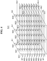
- FIGS. 3 and 4 are diagrams for explaining the memory cell array of FIG. 2 .
- a memory block BLK 1 may be formed in a direction perpendicular to a substrate SUB.
- an n+ doping region 166 including impurities may be formed in the substrate SUB.
- the doping region 166 may be used, for example, as a common source line (CSL of FIG. 4 ).
- Gate electrodes 165 and insulating films 164 may be alternately stacked on the substrate SUB.
- a data storage film 161 may be formed between the gate electrode 165 and the insulating film 164 .
- a pillar may penetrate the gate electrode 165 and the insulating film 164 in the vertical direction.
- the pillar may be formed in a V shape as shown.
- the pillar may pass through the gate electrode 165 and the insulating film 164 and may be connected to the substrate SUB.
- the inside of the pillar may be made up of an insulating material such as silicon oxide with a charging dielectric pattern 163 .
- the outside of the pillar may be made up of a channel semiconductor with a vertical active pattern 162 .
- the gate electrode 165 of the memory block BLK 1 may be connected to the ground selection line GSL, the plurality of word lines WL 1 to WL 8 , and the string selection line SSL.
- the vertical active pattern 162 formed outside the pillar of the memory block BLK 1 and used as the channel may be connected to a plurality of bit lines BL 1 to BL 3 .
- one memory block BLK 1 is shown to have eight word lines WL 1 to WL 8 and three bit lines BL 1 to BL 3 in FIG. 3 , the embodiments are not limited thereto. If necessary, the number of wirings may be implemented with various modifications.
- FIG. 4 is an exemplary equivalent circuit diagram of the memory block BLK 1 .
- cell strings NS 11 to NS 33 may be disposed between the bit lines BL 1 to BL 3 and the common source line CSL.
- Each cell string (e.g., NS 11 ) may include a ground selection transistor GST, a plurality of memory cells MC 1 to MC 8 and a string selection transistor SST.
- the string selection transistor SST may be connected to a string selection line SSL.
- the string selection line SSL may be separated into first to third string selection lines SSL 1 to SSL 3 .
- the ground selection transistor GST may be connected to the ground selection lines GSL 1 to GSL 3 .
- the ground selection lines GSL 1 to GSL 3 may be connected to each other.
- the string selection transistor SST may be connected to the bit line BL, and the ground selection transistor GST may be connected to the common source line CSL.
- each of the string selection transistor SST and the ground selection transistor GST is formed as the same type of transistor as each of the plurality of memory cells MC 1 to MC 8 embodiments are not limited thereto. In some examples, each of the string selection transistor SST and the ground selection transistor GST is formed as a different type of transistor from each of the plurality of memory cells MC 1 to MC 8 .
- the plurality of memory cells MC 1 to MC 8 may be connected to the corresponding word lines WL 1 to WL 8 , respectively.
- a set of memory cells connected to one word line and programmed during the same time period may be called a page.
- the memory block BLK 1 may include a plurality of pages.
- a plurality of pages may be connected to one word line. Referring to FIG. 4 , a word line (e.g., WL 4 ) having the same height from the common source line CSL may be commonly connected to three pages.
- the pages may be units of data programming and reading, and the memory block BLK 1 may be a unit of data erasing.
- the non-volatile memory device performs a program or read operation
- data of page units may be programmed or read.
- data may be erased in memory block units. For example, data stored in all the memory cells MC 1 to MC 8 included in one memory block may be erased at the same time.
- each of the memory cells MC 1 to MC 8 may store one bit of data or data of two bits or more.
- a memory cell that may store data of one bit in one memory cells MC 1 to MC 8 may be called a single level cell (SLC) or a single bit cell.
- a memory cell that may store data of two bits or more in one memory cell may be called a multi-level cell (MLC) or a multi-bit cell.
- MLC multi-level cell
- two page data may be stored in one physical page.
- two page data may be stored in the memory cell MC 4 connected to the word line WL 4 .
- each of the memory cells MC 1 to MC 8 may store data of three bits or more. In this case, three or more page data may be stored in one physical page.
- FIG. 5 is a timing diagram for explaining a program operation of the non-volatile memory device according to some embodiments.
- FIGS. 6 to 9 are diagrams for explaining the program operation of the non-volatile memory device shown in FIG. 5 according to some embodiments.
- FIG. 10 is a timing diagram for explaining a program operation of the non-volatile memory device according to some embodiments.
- control logic circuit 150 may perform a control to apply a program word line voltage with a voltage level changed stepwise to a word line (WLm, hereinafter m is a natural number) connected to a memory cell (MCn, hereinafter n is a natural number) to be programmed, that is, the selected word line WLm.
- WLm word line
- MCn memory cell
- control logic circuit 150 may perform a control to apply a program word line voltage with a voltage level decreased stepwise to the selected word line WLm.
- various program operations may be executed on the selected memory cell MCn, using each time interval (T 1 to T 3 of FIG. 5 and T 11 to T 14 of FIG. 10 ) of the program word line voltage.
- T 1 to T 3 of FIG. 5 and T 11 to T 14 of FIG. 10 time intervals
- program word line voltages having voltage levels different from each other to the selected word line WLm for each time interval (T 1 to T 3 of FIG. 5 and T 11 to T 14 of FIG. 10 ) after one setting-up as shown, the program execution time can be shortened effectively, while executing various program operations.
- the program bit line voltage applied to the bit line (BLq, where q is a natural number) is controlled. This will be described more specifically below.
- the program execution time may be a time period corresponding to the first to third time intervals T 1 to T 3 .
- the program execution time may be a time period corresponding to the fourth to seventh time intervals T 11 to T 14 .
- the program execution time may be a time period corresponding to the first to third time intervals T 1 to T 3 , and the fourth to seventh time intervals T 11 to T 14 .
- a program bit line voltage having a program inhibit voltage level PIVL is applied to the bit lines BLa, BLb, BLc and BLd in the first time interval T 1 .
- no program operation is executed on the memory cells MCn connected to the bit lines BLa, BLb, BLc and BLd.
- the program inhibit voltage level PIVL may be the same as, for example, a power supply voltage VDD level. However, the embodiments are not limited thereto, and the program inhibit voltage level PIVL may be modified variously to be different from this case.
- a program bit line voltage having the program inhibit voltage level PIVL is applied to the bit lines BLb, BLc and BLd.
- the program bit line voltage applied to the bit line BLa transitions from the program inhibit voltage level PIVL to a program voltage level PVL.
- the program operation is executed on the memory cell MCn connected to the bit line BLa.
- the program voltage level PVL may be the same as, for example, a ground voltage GND level.
- the embodiments are not limited thereto, and the program voltage level GND may be modified freely to be different from this case.
- memory cells MCn included in the memory cell group Ga connected to the bit line BLa may be programmed to a first program state P 1 by the program word line voltage and the program bit line voltage shown in FIG. 5 .
- the program bit line voltage applied to the bit line BLb transitions from the program inhibit voltage level PIVL to the program voltage level PVL.
- the program bit line voltage applied to the bit line BLc transitions from the program inhibit voltage level PIVL to a voltage level between the program inhibit voltage level PIVL and the program voltage level PVL.
- the bit lines BLb and BLc may be disposed adjacent to each other.
- the program bit line voltage to be applied to the bit line BLc may be a forcing voltage level FVL which is applied to the bit line BLc to improve the threshold voltage dispersion of the memory cell MCn connected to the bit line BLc.
- FVL forcing voltage level
- the program operation is executed on the memory cells MCn connected to the bit lines BLb and BLc.
- memory cells MCn included in the memory cell group Gb connected to the bit line BLb having a threshold voltage lower than a predetermined threshold voltage Vr 1 may be programmed to a second program state P 2 by the program word line voltage and the program bit line voltage in FIG. 5 .
- memory cells MCn included in the memory cell group Gc connected to the bit line BLc having a threshold voltage higher than a predetermined threshold voltage Vr 1 may also be programmed to the second program state P 2 by the program word line voltage and the program bit line voltage in FIG. 5 .
- the forcing voltage level FVL of the program bit line voltage applied to the memory cells MCn included in the memory cell group Gc may be implemented with various modifications in accordance with the dispersion of the memory cells MCn included in the memory cell group Gb and the memory cells MCn included in the memory cell group Gc. In some examples, the forcing voltage level FVL may be implemented with various modifications even in program examples different from the shown example.
- the program bit line voltage applied to the bit line BLd transitions from the program inhibit voltage level PIVL to a voltage level higher than the program inhibit voltage level PIVL.
- the program bit line voltage applied to the bit line BLd may transition to a voltage level that is higher than the program inhibit voltage level PIVL by a second voltage level difference dV 2 .
- the program bit line voltage to be applied to the bit line BLd may transition to the program inhibit voltage level PIVL as shown.
- the memory cells MCn connected to the bit line BLd may be influenced by the coupling effect. Accordingly, in the present embodiment, in order to minimize such a coupling effect, when the level of the program bit line voltage applied to the bit line BLb decreases, the coupling effect can be prevented by increasing the voltage level of the program bit line voltage to be applied to the bit line BLd adjacent thereto by a second voltage level difference dV 2 .
- the coupling effect occurring between the bit line BLb and the bit line BLd arranged adjacent to each other in this way may also be prevented by controlling the control signal to be applied to the string selection line SSL 1 .
- the coupling effect may be minimized, by turning off selection transistors SSTb and SSTd connected to the bit line BLb and the adjacent bit line BLd, respectively, before the level of the program bit line voltage to be applied to the bit line BLb decreases (that is, before a third time interval T 3 ) to prevent the channels connected to the bit line BLb and the adjacent bit line BLd from coupling.
- selection transistors SSTb and SSTd by turning off selection transistors SSTb and SSTd before the level of the program bit line voltage to be applied to the bit line BLb decreases to the program voltage level (e.g., GND), prevent the bit line voltage connected to the adjacent bit line BLd (i.e., no program memory cells) from some leakage. Thereafter, the selection transistors SSTb and SSTd may be turned on again subsequent to a certain period of time after the voltage level of the program bit line voltage to be applied to the bit line BLd decreases by the second voltage level difference dV 2 (i.e., decreases to the program inhibit voltage level).
- FIG. 9 shows an embodiment in which the voltage level of the string selection signal to be applied to the string selection line SSL 1 transitions as a method of turning off the selection transistors SSTb and SSTd connected to the bit line BLb and the bit line BLd, respectively, the embodiments are not limited thereto.
- the program bit line voltage to be applied to a bit line BLe transitions from a second voltage level 2 VL to a program inhibit voltage level PIVL.
- boosting on the memory cell MCn may be maintained so that the memory cells MCn connected to the bit line BLe and programmed to a specific program state are not influenced by other program operations.
- the configurations shown in FIGS. 5 and 10 are not implemented dividedly in separate embodiments. That is to say, while the program word line voltage with the voltage level decreased stepwise is continuously applied to the selected word line WLm as shown, the program bit line voltage may variously transition in the bit lines BLa to BLh as shown in the first to third time intervals T 1 to T 3 of FIG. 5 and the fourth to seventh time intervals T 11 to T 14 of FIG. 10 .
- all the first to third voltage levels 1 VL to 3 VL shown in FIG. 10 may have voltage levels between the program inhibit voltage level PIVL and the program voltage level PVL.
- the second voltage level 2 VL may be the aforementioned forcing voltage level (FVL of FIG. 5 ), embodiments are not limited thereto.
- each of the first and third voltage levels 1 VL and 3 VL may also be the forcing voltage level.
- the third voltage level 3 VL may be a voltage level having a voltage higher than the second voltage level 2 VL
- the first voltage level 1 VL may be a voltage level having a voltage lower than the second voltage level 2 VL.
- the program bit line voltage to be applied to the bit line BLf maintains the second voltage level 2 VL. Accordingly, for example, a fine program may be continuously executed on the memory cells MCn connected to the bit line BLf.
- the program bit line voltage to be applied to the bit line BLg transitions from the second voltage level 2 VL to the third voltage level 3 VL or transitions from the second voltage level 2 VL to the first voltage level 1 VL. Therefore, for example, a fine program operation required for the memory cells MCn connected to the bit line BLg and released from the program inhibit state may be executed.
- the program bit line voltage to be applied to the bit line BLh transitions from the second voltage level 2 VL to the program voltage level PVL. Therefore, for example, additional program operations may be executed on the memory cells MCn connected to the bit line BLh.
- FIGS. 11 to 16 are flowcharts for explaining the program operation of the non-volatile memory device according to some embodiments.
- a program word line voltage is provided to a selected word line WL of a plurality of word lines (S 100 ).
- a program word line voltage with a voltage level changed stepwise may be provided to the selected word line, for example, WLm.
- the voltage level of the program word line voltage may decrease by a first voltage level difference dV 1 as shown in FIG. 5 , the embodiments are not limited thereto.
- a program bit line voltage is provided to the plurality of bit lines (S 200 ).
- applying the program bit line voltage to the plurality of bit lines may be performed while the program word line voltage is provided to the selected word line WLm. Such an operation is the same in all the embodiments to be described below.
- the program bit line voltage to be provided to the plurality of bit lines BLq may include transitions between various voltage levels.
- FIGS. 12 to 19 a more specific description will be given with reference to FIGS. 12 to 19 .
- a program bit line voltage having a first voltage level is provided to a plurality of bit lines (S 201 ).
- the first voltage level may be a voltage level between a program inhibit voltage level for preventing the memory cells connected to the bit line to which the program bit line voltage is provided from being programmed, and a program voltage level for causing memory cells connected to the bit line to which the program bit line voltage is provided to be programmed.
- such a first voltage level may include a forcing voltage level to be provided to the bit line to improve threshold voltage dispersion of memory cells connected to the bit line to which the program bit line voltage is provided.
- a forcing voltage level to be provided to the bit line to improve threshold voltage dispersion of memory cells connected to the bit line to which the program bit line voltage is provided.
- the embodiments are not limited thereto.
- a program bit line voltage having a program inhibit voltage level is provided to a plurality of bit lines (S 202 ).
- a program bit line voltage having a program inhibit voltage level may be provided to a plurality of bit lines, by transitioning a voltage level of a program bit line voltage to be provided to the bit line from a first level to a program inhibit voltage level.
- a program bit line voltage having a first voltage level is provided to a plurality of bit lines (S 211 ).
- a program bit line having a second voltage level may be provided to a plurality of bit lines, by transitioning a voltage level of a program bit line voltage to be provided to the bit line from a first level to a second voltage level.
- the second voltage level may be a voltage level between the program inhibit voltage level and the program voltage level.
- the second voltage level may be a voltage level having a voltage higher than the first voltage level.
- the second voltage level may be a voltage level having a voltage lower than the first voltage level.
- a program bit line voltage having a first voltage level is provided to a plurality of bit lines (S 221 ).
- a program bit line voltage having a program voltage level is provided to a plurality of bit lines (S 222 ).
- a program bit line voltage having a program voltage level may be provided to a plurality of bit lines, by transitioning a voltage level of a program bit line voltage to be provided to the bit line from the first voltage level to the program voltage level.
- a program bit line voltage having a program inhibit voltage level is provided to a plurality of bit lines (S 231 ).
- a program bit line voltage having a first voltage level is provided to the plurality of bit lines (S 232 ).
- a program bit line voltage having a first voltage level may be provided to a plurality of bit lines, by transitioning a voltage level of a program bit line voltage to be provided to the bit line from the program inhibit voltage level to the first voltage level.
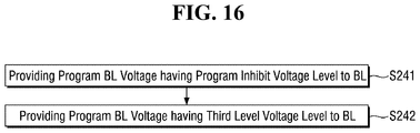
- a program bit line voltage having a program inhibit voltage level is provided to a plurality of bit lines (S 241 ).
- a program bit line voltage having a third voltage level may be provided to a plurality of bit lines, by transitioning a voltage level of a program bit line voltage to be provided to a bit line from the program inhibit voltage level to the third voltage level.
- the third voltage level may be a voltage level having voltage higher than the program inhibit voltage level.
- FIG. 17 is a cross-sectional view illustrating a non-volatile memory device according to some embodiments.
- a non-volatile memory device 4000 may have a chip-to-chip (C2C) structure.
- the C2C structure may refer to a structure formed by manufacturing an upper chip including a cell region CELL on a first wafer, manufacturing a lower chip including a peripheral circuit region PERI on a second wafer, different from the first wafer, and then connecting the upper chip and the lower chip in a bonding manner.
- the bonding manner may include a method of electrically connecting a bonding metal formed on an uppermost metal layer of the upper chip and a bonding metal formed on an uppermost metal layer of the lower chip.
- the bonding metals may be formed of copper (Cu)
- the bonding manner may be a Cu—Cu bonding
- the bonding metals may also be formed of aluminum or tungsten.
- Each of the peripheral circuit region PERI and the cell region CELL of the non-volatile memory device 4000 may include an external pad bonding area PA, a word line bonding area WLBA, and a bit line bonding area BLBA.
- the peripheral circuit region PERI may include a first substrate 4210 , an interlayer insulating layer 4215 , a plurality of circuit elements 4220 a , 4220 b , and 4220 c formed on the first substrate 4210 , first metal layers 4230 a , 4230 b , and 4230 c respectively connected to the plurality of circuit elements 4220 a , 4220 b , and 4220 c , and second metal layers 4240 a , 4240 b , and 4240 c formed on the first metal layers 4230 a , 4230 b , and 4230 c .
- Each of the circuit elements 4220 a , 4220 b , and 4220 c may include one or more transistors.
- the first metal layers 4230 a , 4230 b , and 4230 c may be formed of tungsten having relatively high resistance
- the second metal layers 4240 a , 4240 b , and 4240 c may be formed of copper having relatively low resistance.
- first metal layers 4230 a , 4230 b , and 4230 c and the second metal layers 4240 a , 4240 b , and 4240 c are shown and described, they are not limited thereto, and one or more metal layers may be further formed on the second metal layers 4240 a , 4240 b , and 4240 c . At least a portion of the one or more metal layers formed on the second metal layers 4240 a , 4240 b , and 4240 c may be formed of aluminum or the like having a lower resistance than those of copper forming the second metal layers 4240 a , 4240 b , and 4240 c.
- the interlayer insulating layer 4215 may be disposed on the first substrate 4210 and cover the plurality of circuit elements 4220 a , 4220 b , and 4220 c , the first metal layers 4230 a , 4230 b , and 4230 c , and the second metal layers 4240 a , 4240 b , and 4240 c .
- the interlayer insulating layer 4215 may include an insulating material such as silicon oxide, silicon nitride, or the like.
- Lower bonding metals 4271 b and 4272 b may be formed on the second metal layer 4240 b in the word line bonding area WLBA.
- the lower bonding metals 4271 b and 4272 b in the peripheral circuit region PERI may be electrically connected to upper bonding metals 4371 b and 4372 b in the cell region CELL in a bonding manner, and the lower bonding metals 4271 b and 4272 b and the upper bonding metals 4371 b and 4372 b may be formed of aluminum, copper, tungsten, or the like.
- the upper bonding metals 4371 b and 4372 b in the cell region CELL may be referred as first metal pads and the lower bonding metals 4271 b and 4272 b in the peripheral circuit region PERI may be referred as second metal pads.
- the first metal pads and the second metal pads may be connected with each other in the bonding manner.
- the cell region CELL may include at least one memory block.
- the cell region CELL may include a second substrate 4310 and a common source line 4320 .
- a plurality of word lines 4331 to 4338 i.e., 4330
- At least one string select line and at least one ground select line may be arranged on and below the plurality of word lines 4330 , respectively, and the plurality of word lines 4330 may be disposed between the at least one string select line and the at least one ground select line.
- a channel structure CH may extend in a direction, perpendicular to the upper surface of the second substrate 4310 , and pass through the plurality of word lines 4330 , the at least one string select line, and the at least one ground select line.
- the channel structure CH may include a data storage layer, a channel layer, a buried insulating layer, and the like, and the channel layer may be electrically connected to a third metal layer 4350 c and a fourth metal layer 4360 c .
- the third metal layer 4350 c may be a bit line contact
- the fourth metal layer 4360 c may be a bit line.
- the bit line 4360 c may extend in a first direction (a Y-axis direction), parallel to the upper surface of the second substrate 4310 .
- an area in which the channel structure CH, the bit line 4360 c , and the like are disposed may be defined as the bit line bonding area BLBA.
- the bit line 4360 c may be electrically connected to the circuit elements 4220 c providing a page buffer 4393 in the peripheral circuit region PERI.
- the bit line 4360 c may be connected to upper bonding metals 4371 c and 4372 c in the cell region CELL, and the upper bonding metals 4371 c and 4372 c may be connected to lower bonding metals 4271 c and 4272 c connected to the circuit elements 4220 c of the page buffer 4393 .
- the plurality of word lines 4330 may extend in a second direction (an X-axis direction), parallel to the upper surface of the second substrate 4310 , and may be connected to a plurality of cell contact plugs 4341 to 4347 (i.e., 4340 ).
- the plurality of word lines 4330 and the plurality of cell contact plugs 4340 may be connected to each other in pads provided by at least a portion of the plurality of word lines 4330 extending in different lengths in the second direction.
- a third metal layer 4350 b and a fourth metal layer 4360 b may be connected to an upper portion of the plurality of cell contact plugs 4340 connected to the plurality of word lines 4330 , sequentially.
- the plurality of cell contact plugs 4340 may be connected to the circuit region PERI by the upper bonding metals 4371 b and 4372 b of the cell region CELL and the lower bonding metals 4271 b and 4272 b of the peripheral circuit region PERI in the word line bonding area WLBA.
- the plurality of cell contact plugs 4340 may be electrically connected to the circuit elements 4220 b providing a row decoder 4394 in the peripheral circuit region PERI.
- operating voltages of the circuit elements 4220 b providing the row decoder 4394 may be different than operating voltages of the circuit elements 4220 c providing the page buffer 4393 .
- operating voltages of the circuit elements 4220 c providing the page buffer 4393 may be greater than operating voltages of the circuit elements 4220 b providing the row decoder 4394 .
- a common source line contact plug 4380 may be disposed in the external pad bonding area PA.
- the common source line contact plug 4380 may be formed of a conductive material such as a metal, a metal compound, polysilicon, or the like, and may be electrically connected to the common source line 4320 .
- a third metal layer 4350 a and a fourth metal layer 4360 a may be stacked on an upper portion of the common source line contact plug 4380 , sequentially. For example, an area in which the common source line contact plug 4380 , the third metal layer 4350 a , and the fourth metal layer 4360 a are disposed may be defined as the external pad bonding area PA.
- Input-output pads 4205 and 4305 may be disposed in the external pad bonding area PA.
- a lower insulating film 4201 covering a lower surface of the first substrate 4210 may be formed below the first substrate 4210 , and a first input-output pad 4205 may be formed on the lower insulating film 4201 .
- the first input-output pad 4205 may be connected to at least one of the plurality of circuit elements 4220 a , 4220 b , and 4220 c disposed in the peripheral circuit region PERI through a first input-output contact plug 4203 , and the first input-output pad 4205 may be separated from the first substrate 4210 by the lower insulating film 4201 .
- a side insulating film may be disposed between the first input-output contact plug 4203 and the first substrate 4210 to electrically separate the first input-output contact plug 4203 and the first substrate 4210 .
- an upper insulating film 4301 covering the upper surface of the second substrate 4310 may be formed on the second substrate 4310 , and a second input-output pad 4305 may be disposed on the upper insulating layer 4301 .
- the second input-output pad 4305 may be connected to at least one of the plurality of circuit elements 4220 a , 4220 b , and 4220 c disposed in the peripheral circuit region PERI through a second input-output contact plug 4303 .
- the second substrate 4310 and the common source line 4320 may not be disposed in an area in which the second input-output contact plug 4303 is disposed.
- the second input-output pad 4305 may not overlap the word lines 4330 in the third direction (the Z-axis direction).
- the second input-output contact plug 4303 may be separated from the second substrate 4310 in a direction, parallel to the upper surface of the second substrate 4310 , and may pass through an interlayer insulating layer 4315 of the cell region CELL to be connected to the second input-output pad 4305 and an upper metal pattern 4372 a of the cell region CELL.
- the first input-output pad 4205 and the second input-output pad 4305 may be selectively formed.
- the non-volatile memory device 4000 may include only the first input-output pad 4205 disposed on the first substrate 4210 or the second input-output pad 4305 disposed on the second substrate 4310 .
- the non-volatile memory device 4000 may include both the first input-output pad 4205 and the second input-output pad 4305 .
- a metal pattern in an uppermost metal layer may be provided as a dummy pattern or the uppermost metal layer may be absent, in each of the external pad bonding area PA and the bit line bonding area BLBA, respectively included in the cell region CELL and the peripheral circuit region PERI.
- the non-volatile memory device 4000 may include a lower metal pattern 4273 a , corresponding to the upper metal pattern 4372 a formed in an uppermost metal layer of the cell region CELL, and having the same shape as the upper metal pattern 4372 a of the cell region CELL, in an uppermost metal layer of the peripheral circuit region PERI.
- the lower metal pattern 4273 a formed in the uppermost metal layer of the peripheral circuit region PERI may not be connected to a contact.
- an upper metal pattern corresponding to the lower metal pattern formed in an uppermost metal layer of the peripheral circuit region PERI, and having the same shape as a lower metal pattern of the peripheral circuit region PERI, may be formed in an uppermost metal layer of the cell region CELL.
- the lower bonding metals 4271 b and 4272 b may be formed on the second metal layer 4240 b in the word line bonding area WLBA.
- the lower bonding metals 4271 b and 4272 b of the peripheral circuit region PERI may be electrically connected to the upper bonding metals 4371 b and 4372 b of the cell region CELL by a Cu—Cu bonding.
- bit line bonding area BLBA an upper metal pattern 4392 , corresponding to a lower metal pattern 4252 formed in the uppermost metal layer of the peripheral circuit region PERI, and having the same shape as the lower metal pattern 4252 of the peripheral circuit region PERI, may be formed in an uppermost metal layer of the cell region CELL.
- a contact may not be formed on the upper metal pattern 4392 formed in the uppermost metal layer of the cell region CELL.
- a reinforcement metal pattern having the same shape as the metal pattern may be formed in an uppermost metal layer in another one of the cell region CELL and the peripheral circuit region PERI, and a contact may not be formed on the reinforcement metal pattern.
- the non-volatile memory device 4000 can operate and can include device components according to one or more of the example embodiments described in FIGS. 1 to 16 previously.
Landscapes
- Engineering & Computer Science (AREA)
- Microelectronics & Electronic Packaging (AREA)
- Computer Hardware Design (AREA)
- Power Engineering (AREA)
- Physics & Mathematics (AREA)
- Condensed Matter Physics & Semiconductors (AREA)
- General Physics & Mathematics (AREA)
- Read Only Memory (AREA)
Abstract
Description
Claims (20)
Priority Applications (1)
| Application Number | Priority Date | Filing Date | Title |
|---|---|---|---|
| US16/991,821 US11200952B2 (en) | 2019-07-22 | 2020-08-12 | Non-volatile memory device |
Applications Claiming Priority (4)
| Application Number | Priority Date | Filing Date | Title |
|---|---|---|---|
| KR1020190088372A KR102771883B1 (en) | 2019-07-22 | 2019-07-22 | Non-volatile memory device and method for programming the device |
| KR10-2019-0088372 | 2019-07-22 | ||
| US16/823,275 US11322205B2 (en) | 2019-07-22 | 2020-03-18 | Non-volatile memory device and method for programming the same |
| US16/991,821 US11200952B2 (en) | 2019-07-22 | 2020-08-12 | Non-volatile memory device |
Related Parent Applications (1)
| Application Number | Title | Priority Date | Filing Date |
|---|---|---|---|
| US16/823,275 Continuation-In-Part US11322205B2 (en) | 2019-07-22 | 2020-03-18 | Non-volatile memory device and method for programming the same |
Publications (2)
| Publication Number | Publication Date |
|---|---|
| US20210027841A1 US20210027841A1 (en) | 2021-01-28 |
| US11200952B2 true US11200952B2 (en) | 2021-12-14 |
Family
ID=74189153
Family Applications (1)
| Application Number | Title | Priority Date | Filing Date |
|---|---|---|---|
| US16/991,821 Active US11200952B2 (en) | 2019-07-22 | 2020-08-12 | Non-volatile memory device |
Country Status (1)
| Country | Link |
|---|---|
| US (1) | US11200952B2 (en) |
Families Citing this family (2)
| Publication number | Priority date | Publication date | Assignee | Title |
|---|---|---|---|---|
| CN116784011A (en) * | 2021-02-03 | 2023-09-19 | 铠侠股份有限公司 | Semiconductor memory device |
| US12340845B2 (en) * | 2021-06-09 | 2025-06-24 | Sk Hynix Nand Product Solutions Corp. | Split block array for 3D NAND memory |
Citations (39)
| Publication number | Priority date | Publication date | Assignee | Title |
|---|---|---|---|---|
| US20040240269A1 (en) | 2001-09-17 | 2004-12-02 | Raul-Adrian Cernea | Latched programming of memory and method |
| US7085157B2 (en) | 2003-04-04 | 2006-08-01 | Renesas Technology Corp. | Nonvolatile memory device and semiconductor device |
| US20080279012A1 (en) | 2007-05-10 | 2008-11-13 | Samsung Electronics Co., Ltd. | Methods of Operating Memory Devices Including Negative Incremental Step Pulse Programming and Related Devices |
| US7715235B2 (en) | 2008-08-25 | 2010-05-11 | Sandisk Corporation | Non-volatile memory and method for ramp-down programming |
| US7764542B2 (en) | 2007-04-03 | 2010-07-27 | Kabushiki Kaisha Toshiba | Method for programming a semiconductor memory device |
| US20110069546A1 (en) | 2009-09-24 | 2011-03-24 | Kabushiki Kaisha Toshiba | Nonvolatile semiconductor memory device |
| US8023312B2 (en) * | 2006-12-08 | 2011-09-20 | Sharp Kabushiki Kaisha | Nonvolatile semiconductor memory device |
| US20110267895A1 (en) | 2010-04-29 | 2011-11-03 | Min Kyu Lee | Method of operating semiconductor memory device |
| US8218381B2 (en) * | 2009-11-24 | 2012-07-10 | Sandisk Technologies Inc. | Programming memory with sensing-based bit line compensation to reduce channel-to-floating gate coupling |
| US20120287720A1 (en) | 2011-05-11 | 2012-11-15 | SK Hynix Inc. | Semiconductor memory device and method of programming the same |
| US20130135937A1 (en) * | 2011-11-29 | 2013-05-30 | Micron Technoloy, Inc. | Programming memory cells using smaller step voltages for higher program levels |
| US9159424B2 (en) * | 2013-06-28 | 2015-10-13 | SK Hynix Inc. | Three dimensional semiconductor memory device with line sharing scheme |
| US9230677B2 (en) * | 2013-07-25 | 2016-01-05 | Aplus Flash Technology, Inc | NAND array hiarchical BL structures for multiple-WL and all-BL simultaneous erase, erase-verify, program, program-verify, and read operations |
| US9263137B2 (en) * | 2013-06-27 | 2016-02-16 | Aplus Flash Technology, Inc. | NAND array architecture for multiple simutaneous program and read |
| US9396791B2 (en) | 2014-07-18 | 2016-07-19 | Micron Technology, Inc. | Programming memories with multi-level pass signal |
| US9406393B2 (en) * | 2014-08-25 | 2016-08-02 | Samsung Electronics Co., Ltd. | Nonvolatile memory devices and program verification methods using one verification voltage to verify memory cells having different target states |
| US9466389B2 (en) * | 2014-07-07 | 2016-10-11 | SK Hynix Inc. | Multiple programming pulse per loop programming and verification method for non-volatile memory devices |
| US9633732B2 (en) * | 2015-09-24 | 2017-04-25 | SK Hynix Inc. | Semiconductor memory device and operating method thereof |
| US9767909B1 (en) | 2016-03-17 | 2017-09-19 | Micron Technology, Inc. | Memory cell programming utilizing conditional enabling of memory cells |
| US9842657B1 (en) | 2017-05-18 | 2017-12-12 | Sandisk Technologies Llc | Multi-state program using controlled weak boosting for non-volatile memory |
| US9947418B2 (en) | 2016-04-12 | 2018-04-17 | Micron Technology, Inc. | Boosted channel programming of memory |
| US10037797B2 (en) | 2014-06-09 | 2018-07-31 | Micron Technology, Inc. | Programming memories with stepped programming pulses including inhibiting a memory cell for a portion of a programming pulse and enabling that memory cell for another portion of that programming pulse |
| US10170188B1 (en) * | 2017-08-31 | 2019-01-01 | Micron Technology, Inc. | 3D memory device including shared select gate connections between memory blocks |
| US20190057742A1 (en) * | 2017-08-17 | 2019-02-21 | Samsung Electronics Co, Ltd | Nonvolatile memory device and method of operating the same |
| US20190066818A1 (en) * | 2017-08-22 | 2019-02-28 | Sandisk Technologies Llc | Determination of fast to program word lines in non-volatile memory |
| US20190080727A1 (en) * | 2017-09-08 | 2019-03-14 | Toshiba Memory Corporation | Control method for memory device |
| US20190088342A1 (en) * | 2017-09-20 | 2019-03-21 | Toshiba Memory Corporation | Semiconductor memory device |
| US20190088312A1 (en) * | 2017-09-20 | 2019-03-21 | Toshiba Memory Corporation | Semiconductor memory device |
| US20190139609A1 (en) * | 2017-11-03 | 2019-05-09 | SK Hynix Inc. | Semiconductor memory device and operating method thereof |
| US20190189218A1 (en) * | 2017-12-19 | 2019-06-20 | Toshiba Memory Corporation | Semiconductor memory device |
| US20190296040A1 (en) * | 2018-03-22 | 2019-09-26 | Toshiba Memory Corporation | Semiconductor memory |
| US20190348131A1 (en) * | 2018-05-14 | 2019-11-14 | Toshiba Memory Corporation | Semiconductor memory device |
| US20190371406A1 (en) * | 2018-06-05 | 2019-12-05 | Sandisk Technologies Llc | Memory device with connected word lines for fast programming |
| US20190378580A1 (en) * | 2018-06-07 | 2019-12-12 | Sandisk Technologies Llc | Non-volatile memory with countermeasure for program disturb including purge during precharge |
| US20190378581A1 (en) * | 2018-06-07 | 2019-12-12 | Sandisk Technologies Llc | Non-volatile memory with countermeasure for program disturb including spike during boosting |
| US20190392909A1 (en) * | 2018-06-21 | 2019-12-26 | Sandisk Technologies Llc | Interleaved program and verify in non-volatile memory |
| US20190392908A1 (en) * | 2017-11-14 | 2019-12-26 | Samsung Electronics Co., Ltd. | Nonvolatile memory device and operating method thereof |
| US10795762B2 (en) * | 2018-01-31 | 2020-10-06 | SK Hynix Inc. | Memory controller and method of operating the same |
| US10937503B2 (en) * | 2019-06-17 | 2021-03-02 | SK Hynix Inc. | Memory device and method of operating the same |
-
2020
- 2020-08-12 US US16/991,821 patent/US11200952B2/en active Active
Patent Citations (39)
| Publication number | Priority date | Publication date | Assignee | Title |
|---|---|---|---|---|
| US20040240269A1 (en) | 2001-09-17 | 2004-12-02 | Raul-Adrian Cernea | Latched programming of memory and method |
| US7085157B2 (en) | 2003-04-04 | 2006-08-01 | Renesas Technology Corp. | Nonvolatile memory device and semiconductor device |
| US8023312B2 (en) * | 2006-12-08 | 2011-09-20 | Sharp Kabushiki Kaisha | Nonvolatile semiconductor memory device |
| US7764542B2 (en) | 2007-04-03 | 2010-07-27 | Kabushiki Kaisha Toshiba | Method for programming a semiconductor memory device |
| US20080279012A1 (en) | 2007-05-10 | 2008-11-13 | Samsung Electronics Co., Ltd. | Methods of Operating Memory Devices Including Negative Incremental Step Pulse Programming and Related Devices |
| US7715235B2 (en) | 2008-08-25 | 2010-05-11 | Sandisk Corporation | Non-volatile memory and method for ramp-down programming |
| US20110069546A1 (en) | 2009-09-24 | 2011-03-24 | Kabushiki Kaisha Toshiba | Nonvolatile semiconductor memory device |
| US8218381B2 (en) * | 2009-11-24 | 2012-07-10 | Sandisk Technologies Inc. | Programming memory with sensing-based bit line compensation to reduce channel-to-floating gate coupling |
| US20110267895A1 (en) | 2010-04-29 | 2011-11-03 | Min Kyu Lee | Method of operating semiconductor memory device |
| US20120287720A1 (en) | 2011-05-11 | 2012-11-15 | SK Hynix Inc. | Semiconductor memory device and method of programming the same |
| US20130135937A1 (en) * | 2011-11-29 | 2013-05-30 | Micron Technoloy, Inc. | Programming memory cells using smaller step voltages for higher program levels |
| US9263137B2 (en) * | 2013-06-27 | 2016-02-16 | Aplus Flash Technology, Inc. | NAND array architecture for multiple simutaneous program and read |
| US9159424B2 (en) * | 2013-06-28 | 2015-10-13 | SK Hynix Inc. | Three dimensional semiconductor memory device with line sharing scheme |
| US9230677B2 (en) * | 2013-07-25 | 2016-01-05 | Aplus Flash Technology, Inc | NAND array hiarchical BL structures for multiple-WL and all-BL simultaneous erase, erase-verify, program, program-verify, and read operations |
| US10037797B2 (en) | 2014-06-09 | 2018-07-31 | Micron Technology, Inc. | Programming memories with stepped programming pulses including inhibiting a memory cell for a portion of a programming pulse and enabling that memory cell for another portion of that programming pulse |
| US9466389B2 (en) * | 2014-07-07 | 2016-10-11 | SK Hynix Inc. | Multiple programming pulse per loop programming and verification method for non-volatile memory devices |
| US9396791B2 (en) | 2014-07-18 | 2016-07-19 | Micron Technology, Inc. | Programming memories with multi-level pass signal |
| US9406393B2 (en) * | 2014-08-25 | 2016-08-02 | Samsung Electronics Co., Ltd. | Nonvolatile memory devices and program verification methods using one verification voltage to verify memory cells having different target states |
| US9633732B2 (en) * | 2015-09-24 | 2017-04-25 | SK Hynix Inc. | Semiconductor memory device and operating method thereof |
| US9767909B1 (en) | 2016-03-17 | 2017-09-19 | Micron Technology, Inc. | Memory cell programming utilizing conditional enabling of memory cells |
| US9947418B2 (en) | 2016-04-12 | 2018-04-17 | Micron Technology, Inc. | Boosted channel programming of memory |
| US9842657B1 (en) | 2017-05-18 | 2017-12-12 | Sandisk Technologies Llc | Multi-state program using controlled weak boosting for non-volatile memory |
| US20190057742A1 (en) * | 2017-08-17 | 2019-02-21 | Samsung Electronics Co, Ltd | Nonvolatile memory device and method of operating the same |
| US20190066818A1 (en) * | 2017-08-22 | 2019-02-28 | Sandisk Technologies Llc | Determination of fast to program word lines in non-volatile memory |
| US10170188B1 (en) * | 2017-08-31 | 2019-01-01 | Micron Technology, Inc. | 3D memory device including shared select gate connections between memory blocks |
| US20190080727A1 (en) * | 2017-09-08 | 2019-03-14 | Toshiba Memory Corporation | Control method for memory device |
| US20190088342A1 (en) * | 2017-09-20 | 2019-03-21 | Toshiba Memory Corporation | Semiconductor memory device |
| US20190088312A1 (en) * | 2017-09-20 | 2019-03-21 | Toshiba Memory Corporation | Semiconductor memory device |
| US20190139609A1 (en) * | 2017-11-03 | 2019-05-09 | SK Hynix Inc. | Semiconductor memory device and operating method thereof |
| US20190392908A1 (en) * | 2017-11-14 | 2019-12-26 | Samsung Electronics Co., Ltd. | Nonvolatile memory device and operating method thereof |
| US20190189218A1 (en) * | 2017-12-19 | 2019-06-20 | Toshiba Memory Corporation | Semiconductor memory device |
| US10795762B2 (en) * | 2018-01-31 | 2020-10-06 | SK Hynix Inc. | Memory controller and method of operating the same |
| US20190296040A1 (en) * | 2018-03-22 | 2019-09-26 | Toshiba Memory Corporation | Semiconductor memory |
| US20190348131A1 (en) * | 2018-05-14 | 2019-11-14 | Toshiba Memory Corporation | Semiconductor memory device |
| US20190371406A1 (en) * | 2018-06-05 | 2019-12-05 | Sandisk Technologies Llc | Memory device with connected word lines for fast programming |
| US20190378580A1 (en) * | 2018-06-07 | 2019-12-12 | Sandisk Technologies Llc | Non-volatile memory with countermeasure for program disturb including purge during precharge |
| US20190378581A1 (en) * | 2018-06-07 | 2019-12-12 | Sandisk Technologies Llc | Non-volatile memory with countermeasure for program disturb including spike during boosting |
| US20190392909A1 (en) * | 2018-06-21 | 2019-12-26 | Sandisk Technologies Llc | Interleaved program and verify in non-volatile memory |
| US10937503B2 (en) * | 2019-06-17 | 2021-03-02 | SK Hynix Inc. | Memory device and method of operating the same |
Also Published As
| Publication number | Publication date |
|---|---|
| US20210027841A1 (en) | 2021-01-28 |
Similar Documents
| Publication | Publication Date | Title |
|---|---|---|
| US12159675B2 (en) | Nonvolatile memory device including a logic circuit to control word line voltages | |
| US10964398B2 (en) | Memory device and a storage system using the same | |
| US10796766B2 (en) | Nonvolatile memory device and a method of programming the nonvolatile memory device | |
| US10529431B2 (en) | Nonvolatile memory device for performing a partial read operation and a method of reading the same | |
| US11170856B2 (en) | Memory device and a storage system using the same | |
| US12087367B2 (en) | Non-volatile memory device and method of operating the same | |
| US20230154542A1 (en) | Non-volatile memory device and erase method thereof | |
| US11315646B2 (en) | Memory device having improved data reliability by varying program sequences | |
| US11200952B2 (en) | Non-volatile memory device | |
| US11929118B2 (en) | Non-volatile memory device | |
| US12176036B2 (en) | Memory device for controlling word line voltage and operating method thereof | |
| US11322205B2 (en) | Non-volatile memory device and method for programming the same | |
| US11594286B2 (en) | Non-volatile memory device and method of operating the same | |
| US11205485B2 (en) | Three-dimensional NAND flash memory device having improved data reliability by varying program intervals, and method of operating the same | |
| US20240233831A1 (en) | Non-volatile memory device and operating method thereof | |
| US20260045309A1 (en) | Memory device and programming method of memory device | |
| US20250218516A1 (en) | Memory device, memory system including the same, and operating method of the memory device | |
| US20250157542A1 (en) | Non-volatile memory device and programming method | |
| KR20230071034A (en) | Nonvolatile memory device and erasing method of nonvolatile memory device |
Legal Events
| Date | Code | Title | Description |
|---|---|---|---|
| FEPP | Fee payment procedure |
Free format text: ENTITY STATUS SET TO UNDISCOUNTED (ORIGINAL EVENT CODE: BIG.); ENTITY STATUS OF PATENT OWNER: LARGE ENTITY |
|
| AS | Assignment |
Owner name: SAMSUNG ELECTRONICS CO., LTD., KOREA, REPUBLIC OF Free format text: ASSIGNMENT OF ASSIGNORS INTEREST;ASSIGNORS:PARK, SANG-WON;NAM, SANG-WAN;SHIN, JI YEON;AND OTHERS;SIGNING DATES FROM 20200803 TO 20200805;REEL/FRAME:053694/0783 |
|
| STPP | Information on status: patent application and granting procedure in general |
Free format text: DOCKETED NEW CASE - READY FOR EXAMINATION |
|
| STPP | Information on status: patent application and granting procedure in general |
Free format text: NON FINAL ACTION MAILED |
|
| STPP | Information on status: patent application and granting procedure in general |
Free format text: RESPONSE TO NON-FINAL OFFICE ACTION ENTERED AND FORWARDED TO EXAMINER |
|
| STPP | Information on status: patent application and granting procedure in general |
Free format text: NOTICE OF ALLOWANCE MAILED -- APPLICATION RECEIVED IN OFFICE OF PUBLICATIONS |
|
| STPP | Information on status: patent application and granting procedure in general |
Free format text: NOTICE OF ALLOWANCE MAILED -- APPLICATION RECEIVED IN OFFICE OF PUBLICATIONS |
|
| STPP | Information on status: patent application and granting procedure in general |
Free format text: PUBLICATIONS -- ISSUE FEE PAYMENT VERIFIED |
|
| STCF | Information on status: patent grant |
Free format text: PATENTED CASE |
|
| MAFP | Maintenance fee payment |
Free format text: PAYMENT OF MAINTENANCE FEE, 4TH YEAR, LARGE ENTITY (ORIGINAL EVENT CODE: M1551); ENTITY STATUS OF PATENT OWNER: LARGE ENTITY Year of fee payment: 4 |