US11174259B2 - Organic electroluminescent materials and devices - Google Patents
Organic electroluminescent materials and devices Download PDFInfo
- Publication number
- US11174259B2 US11174259B2 US15/983,344 US201815983344A US11174259B2 US 11174259 B2 US11174259 B2 US 11174259B2 US 201815983344 A US201815983344 A US 201815983344A US 11174259 B2 US11174259 B2 US 11174259B2
- Authority
- US
- United States
- Prior art keywords
- group
- aryl
- heteroaryl
- combinations
- alkyl
- Prior art date
- Legal status (The legal status is an assumption and is not a legal conclusion. Google has not performed a legal analysis and makes no representation as to the accuracy of the status listed.)
- Active, expires
Links
- 0 [1*]C1=CC=CC2=C1N=C1[Y]C3=C(C=CC=C3)N12 Chemical compound [1*]C1=CC=CC2=C1N=C1[Y]C3=C(C=CC=C3)N12 0.000 description 13
- HQVUVEHTHLVZEZ-UHFFFAOYSA-N C1=CC=CC=C1.C1=CCC=C1.C1=CN2C=CCC2=C1 Chemical compound C1=CC=CC=C1.C1=CCC=C1.C1=CN2C=CCC2=C1 HQVUVEHTHLVZEZ-UHFFFAOYSA-N 0.000 description 10
- ASVPVWWTSQQNNA-ZRSAMKAJSA-N C1=CC2=C(C=C1)C1(C3=C(C=CC=C3)C2)C2=C(C=CC=C2)[W]C2=C1C=CC=C2.C1=CC2=C(C=C1)C1=C(C2)[W]C2=C1C=CC=C2.C1=CC2=C(C=C1)C1=C(C=CC=C1)C1=C(/C=C/C=C/1)C1=C2C=CC=C1.C1=CC2=C(C=C1)C1=C(C=CC=C1)C2.C1=CC2=C(C=C1)C1=C([W]2)C2=C(/C=C\C=C/2)C1.C1=CC2=C(C=C1)N1C(=NC3=C1C=CC=C3)C2.C1=CC2=C(C=C1)[W]C1=C(C=CC=C1)C2.C1=CC=C(C2=C(C3=CC=CC=C3)C(C3=CC=CC=C3)=C(C3=CC=CC=C3)C(C3=CC=CC=C3)=C2C2=CC=CC=C2)C=C1 Chemical compound C1=CC2=C(C=C1)C1(C3=C(C=CC=C3)C2)C2=C(C=CC=C2)[W]C2=C1C=CC=C2.C1=CC2=C(C=C1)C1=C(C2)[W]C2=C1C=CC=C2.C1=CC2=C(C=C1)C1=C(C=CC=C1)C1=C(/C=C/C=C/1)C1=C2C=CC=C1.C1=CC2=C(C=C1)C1=C(C=CC=C1)C2.C1=CC2=C(C=C1)C1=C([W]2)C2=C(/C=C\C=C/2)C1.C1=CC2=C(C=C1)N1C(=NC3=C1C=CC=C3)C2.C1=CC2=C(C=C1)[W]C1=C(C=CC=C1)C2.C1=CC=C(C2=C(C3=CC=CC=C3)C(C3=CC=CC=C3)=C(C3=CC=CC=C3)C(C3=CC=CC=C3)=C2C2=CC=CC=C2)C=C1 ASVPVWWTSQQNNA-ZRSAMKAJSA-N 0.000 description 6
- LUGCCZZORMAXQA-YQKBRPEESA-N C1=CC2=C(C=C1)C1(C3=C(C=CC=C3)C2)C2=C(C=CC=C2)[W]C2=C1C=CC=C2.C1=CC2=C(C=C1)C1=C(C2)[W]C2=C1C=CC=C2.C1=CC2=C(C=C1)C1=C(C=CC=C1)C1=C(C=CC=C1)C1=C2C=CC=C1.C1=CC2=C(C=C1)C1=C(C=CC=C1)C2.C1=CC2=C(C=C1)C1=C([W]2)C2=C(/C=C\C=C/2)C1.C1=CC2=C(C=C1)N1C(=NC3=C1C=CC=C3)C2.C1=CC2=C(C=C1)[W]C1=C(C=CC=C1)C2.C1=CC=C(C2=C(C3=CC=CC=C3)C(C3=CC=CC=C3)=C(C3=CC=CC=C3)C(C3=CC=CC=C3)=C2C2=CC=CC=C2)C=C1.C1=CC=C(C2=CC(C3=CC=CC=C3)=C(C3=CC=CC=C3)C(C3=CC=CC=C3)=C2C2=CC=CC=C2)C=C1 Chemical compound C1=CC2=C(C=C1)C1(C3=C(C=CC=C3)C2)C2=C(C=CC=C2)[W]C2=C1C=CC=C2.C1=CC2=C(C=C1)C1=C(C2)[W]C2=C1C=CC=C2.C1=CC2=C(C=C1)C1=C(C=CC=C1)C1=C(C=CC=C1)C1=C2C=CC=C1.C1=CC2=C(C=C1)C1=C(C=CC=C1)C2.C1=CC2=C(C=C1)C1=C([W]2)C2=C(/C=C\C=C/2)C1.C1=CC2=C(C=C1)N1C(=NC3=C1C=CC=C3)C2.C1=CC2=C(C=C1)[W]C1=C(C=CC=C1)C2.C1=CC=C(C2=C(C3=CC=CC=C3)C(C3=CC=CC=C3)=C(C3=CC=CC=C3)C(C3=CC=CC=C3)=C2C2=CC=CC=C2)C=C1.C1=CC=C(C2=CC(C3=CC=CC=C3)=C(C3=CC=CC=C3)C(C3=CC=CC=C3)=C2C2=CC=CC=C2)C=C1 LUGCCZZORMAXQA-YQKBRPEESA-N 0.000 description 4
- PECFZCLCYUTIGR-UHFFFAOYSA-N C1=CC=C(C2=CC(C3=CC=CC=C3)=C(C3=CC=CC=C3)C(C3=CC=CC=C3)=C2C2=CC=CC=C2)C=C1.C1=CC=C(C2=CC(C3=CC=CC=C3)=C(C3=CC=CC=C3)C=C2C2=CC=CC=C2)C=C1 Chemical compound C1=CC=C(C2=CC(C3=CC=CC=C3)=C(C3=CC=CC=C3)C(C3=CC=CC=C3)=C2C2=CC=CC=C2)C=C1.C1=CC=C(C2=CC(C3=CC=CC=C3)=C(C3=CC=CC=C3)C=C2C2=CC=CC=C2)C=C1 PECFZCLCYUTIGR-UHFFFAOYSA-N 0.000 description 4
- JTXZAAHCKALMFR-UHFFFAOYSA-N C1=CC=C(C2=CC(C3=CC=CC=C3)=C(C3=CC=CC=C3)C=C2C2=CC=CC=C2)C=C1 Chemical compound C1=CC=C(C2=CC(C3=CC=CC=C3)=C(C3=CC=CC=C3)C=C2C2=CC=CC=C2)C=C1 JTXZAAHCKALMFR-UHFFFAOYSA-N 0.000 description 4
- UNRDJKCHMPBMJW-UHFFFAOYSA-N C.C1=CC=C(C2=CC(C3=CC=CC=C3)=C(C3=CC=CC=C3)C(C3=CC=CC=C3)=C2C2=CC=CC=C2)C=C1.C1=CC=C(C2=CC(C3=CC=CC=C3)=C(C3=CC=CC=C3)C=C2C2=CC=CC=C2)C=C1 Chemical compound C.C1=CC=C(C2=CC(C3=CC=CC=C3)=C(C3=CC=CC=C3)C(C3=CC=CC=C3)=C2C2=CC=CC=C2)C=C1.C1=CC=C(C2=CC(C3=CC=CC=C3)=C(C3=CC=CC=C3)C=C2C2=CC=CC=C2)C=C1 UNRDJKCHMPBMJW-UHFFFAOYSA-N 0.000 description 2
- UREDVTUFFYZMJV-UHFFFAOYSA-N C.CC.CC.CC.CC.CC.CC.CC.CC.CC.CC.CC.CC.CC.CC.CC.CC.CC.CC1=C(C2=N(C)C3=C(C=CC=C3)N2C2=CC=CC=C2)C=CC=C1.CC1=C(C2=N(C)C=CC=C2)C2=C(C=C1)C1=C(C=CC=C1)C2.CC1=C(C2=N(C)C=CC=C2)C=CC=C1.CC1=C(C2=N(C)C=CN2C2=CC=CC=C2)C=CC=C1.CC1=C2C(=CC=C1)C1=CC=CC=C1N1C3=C(C=CC=C3)N(C)=C21.CC1=C2C(=CC=C1)C1=CC=CC=C1N1C=CN(C)=C21 Chemical compound C.CC.CC.CC.CC.CC.CC.CC.CC.CC.CC.CC.CC.CC.CC.CC.CC.CC.CC1=C(C2=N(C)C3=C(C=CC=C3)N2C2=CC=CC=C2)C=CC=C1.CC1=C(C2=N(C)C=CC=C2)C2=C(C=C1)C1=C(C=CC=C1)C2.CC1=C(C2=N(C)C=CC=C2)C=CC=C1.CC1=C(C2=N(C)C=CN2C2=CC=CC=C2)C=CC=C1.CC1=C2C(=CC=C1)C1=CC=CC=C1N1C3=C(C=CC=C3)N(C)=C21.CC1=C2C(=CC=C1)C1=CC=CC=C1N1C=CN(C)=C21 UREDVTUFFYZMJV-UHFFFAOYSA-N 0.000 description 2
- NIJBSMVYHGNZDQ-UHFFFAOYSA-N C1=CC=C(CC2=CC=CC3=C2N=C2N(C4=CC(N5C6=NC7=C(C=CC=C7CC7=NC=CC=C7)N6C6=C5C=CC=C6)=CC=C4)C4=C(C=CC=C4)N23)N=C1.C1=CC=C(CC2=CC=CC3=C2N=C2N(C4=CC=CC(N5C6=NC7=C(C=CC=C7CC7=CC=CC=C7)N6C6=C5C=CC=C6)=C4)C4=C(C=CC=C4)N23)C=C1.C1=CN=C(CC2=CC=CC3=C2N=C2N(C4=CC=CC(N5C6=NC7=C(C=CC=C7CC7=NC=CC=N7)N6C6=C5C=CC=C6)=C4)C4=C(C=CC=C4)N23)N=C1 Chemical compound C1=CC=C(CC2=CC=CC3=C2N=C2N(C4=CC(N5C6=NC7=C(C=CC=C7CC7=NC=CC=C7)N6C6=C5C=CC=C6)=CC=C4)C4=C(C=CC=C4)N23)N=C1.C1=CC=C(CC2=CC=CC3=C2N=C2N(C4=CC=CC(N5C6=NC7=C(C=CC=C7CC7=CC=CC=C7)N6C6=C5C=CC=C6)=C4)C4=C(C=CC=C4)N23)C=C1.C1=CN=C(CC2=CC=CC3=C2N=C2N(C4=CC=CC(N5C6=NC7=C(C=CC=C7CC7=NC=CC=N7)N6C6=C5C=CC=C6)=C4)C4=C(C=CC=C4)N23)N=C1 NIJBSMVYHGNZDQ-UHFFFAOYSA-N 0.000 description 2
- JDFHOLPCMZRJBW-GADBPENTSA-N C1=CC=C2C(=C1)C1=C(C=CC=C1)C1=C(C=CC=C1)C1=C2C=C(N2C3=NC4=C(C=CC=C4CC4=COC=C4)N3C3=C2C=CC=C3)C=C1.C1=CC=C2C(=C1)C1=C(C=CC=C1)C1=C(C=CC=C1)C1=C2C=C(N2C3=NC4=C(C=CC=C4CC4=CSC=C4)N3C3=C2C=CC=C3)C=C1.C1=CC=C2C(=C1)C1=C(C=CC=C1)C1=C(C=CC=C1)C1=C2C=C(N2C3=NC4=C(C=CC=C4CC4=NC=CO4)N3C3=C2C=CC=C3)C=C1.C1=CC=C2C(=C1)C1=C(C=CC=C1)C1=C(C=CC=C1)C1=C2C=C(N2C3=NC4=C(C=CC=C4CC4=NC=NO4)N3C3=C2C=CC=C3)C=C1.C1=CC=C2C(=C1)C1=C(C=CC=C1)C1=C(C=CC=C1)C1=C2C=C(N2C3=NC4=C(C=CC=C4CC4=NCC=N4)N3C3=C2C=CC=C3)C=C1 Chemical compound C1=CC=C2C(=C1)C1=C(C=CC=C1)C1=C(C=CC=C1)C1=C2C=C(N2C3=NC4=C(C=CC=C4CC4=COC=C4)N3C3=C2C=CC=C3)C=C1.C1=CC=C2C(=C1)C1=C(C=CC=C1)C1=C(C=CC=C1)C1=C2C=C(N2C3=NC4=C(C=CC=C4CC4=CSC=C4)N3C3=C2C=CC=C3)C=C1.C1=CC=C2C(=C1)C1=C(C=CC=C1)C1=C(C=CC=C1)C1=C2C=C(N2C3=NC4=C(C=CC=C4CC4=NC=CO4)N3C3=C2C=CC=C3)C=C1.C1=CC=C2C(=C1)C1=C(C=CC=C1)C1=C(C=CC=C1)C1=C2C=C(N2C3=NC4=C(C=CC=C4CC4=NC=NO4)N3C3=C2C=CC=C3)C=C1.C1=CC=C2C(=C1)C1=C(C=CC=C1)C1=C(C=CC=C1)C1=C2C=C(N2C3=NC4=C(C=CC=C4CC4=NCC=N4)N3C3=C2C=CC=C3)C=C1 JDFHOLPCMZRJBW-GADBPENTSA-N 0.000 description 2
- OBYBXDZBRPYNTL-VSMHMLCNSA-N CC.CC.CC.CC.CC.CC.CC.CC.CC.CC.CC.CC.CC.CC.CC.CC.CC.CC.CC.CC.CC1=C(C2=N(C)C3=C(C=CC=C3)C=C2)C=CC=C1.CC1=C(C2=N(C)C=C3C=CC=CC3=C2)C=CC=C1.CC1=C(C2=N(C)C=CC3=C2C=CC=C3)C=CC=C1.CC1=C(C2=N(C)C=CC3=C2CC=C3)C=CC=C1.CC1=C(N2C3=C(C=CC=C3)N(C)[C@@H]2C)C=CC=C1.CC1=C(N2C=CC=N2C)C=CC=C1.CC1=C(N2C=CN(C)[C@@H]2C)C=CC=C1.CC1=C2C(=CC=C1)C1=C(C=CC=C1)C1=CC=N(C)N12.CC1=C2C(=CC=C1)C1=C(C=CC=C1)C1=CN(C)[C@H](C)N12 Chemical compound CC.CC.CC.CC.CC.CC.CC.CC.CC.CC.CC.CC.CC.CC.CC.CC.CC.CC.CC.CC.CC1=C(C2=N(C)C3=C(C=CC=C3)C=C2)C=CC=C1.CC1=C(C2=N(C)C=C3C=CC=CC3=C2)C=CC=C1.CC1=C(C2=N(C)C=CC3=C2C=CC=C3)C=CC=C1.CC1=C(C2=N(C)C=CC3=C2CC=C3)C=CC=C1.CC1=C(N2C3=C(C=CC=C3)N(C)[C@@H]2C)C=CC=C1.CC1=C(N2C=CC=N2C)C=CC=C1.CC1=C(N2C=CN(C)[C@@H]2C)C=CC=C1.CC1=C2C(=CC=C1)C1=C(C=CC=C1)C1=CC=N(C)N12.CC1=C2C(=CC=C1)C1=C(C=CC=C1)C1=CN(C)[C@H](C)N12 OBYBXDZBRPYNTL-VSMHMLCNSA-N 0.000 description 2
- LGNDIALZDXPRIP-UHFFFAOYSA-N CC.CC.CC.CC.CC.CC.CC.CC.CC.CC1=CC=CC2=C1N(C1=N(C)C=CC=C1)C1=CC=CC=C12.CC1=CC=CC2=C1N(C1=N(C)C=CN1C)C1=CC=CC=C12.CC1=CC=CC=C1N1C2=CC=CC=C2C2=C1N(C)=CC=C2 Chemical compound CC.CC.CC.CC.CC.CC.CC.CC.CC.CC1=CC=CC2=C1N(C1=N(C)C=CC=C1)C1=CC=CC=C12.CC1=CC=CC2=C1N(C1=N(C)C=CN1C)C1=CC=CC=C12.CC1=CC=CC=C1N1C2=CC=CC=C2C2=C1N(C)=CC=C2 LGNDIALZDXPRIP-UHFFFAOYSA-N 0.000 description 2
- ATUOYWHBWRKTHZ-UHFFFAOYSA-N CCC Chemical compound CCC ATUOYWHBWRKTHZ-UHFFFAOYSA-N 0.000 description 2
- YXFVVABEGXRONW-UHFFFAOYSA-N Cc1ccccc1 Chemical compound Cc1ccccc1 YXFVVABEGXRONW-UHFFFAOYSA-N 0.000 description 2
- XNPRDOKOGYRMDG-BWYPPSQMSA-N [2H]C([2H])([2H])C1=CC=CC2=C1N=C1N(C3=C(C)C(C4=C(C)C=CC(N5C6=C(C=CC=C6)N6C7=C(/N=C/56)C(C)=CC=C7)=C4C)=C(C)C=C3)C3=C(C=CC=C3)N12.[2H]C([2H])([2H])C1=CC=CC2=C1N=C1N(C3=CC(C)=C(C4=C(C)C=C(N5C6=C(C=CC=C6)N6C7=C(/N=C/56)C(C)=CC=C7)C=C4C)C(C)=C3)C3=C(C=CC=C3)N12.[2H]C([2H])([2H])C1=CC=CC2=C1N=C1N(C3=CC(C4=CC=CC(N5C6=C(C=CC=C6)N6C7=C(/N=C/56)C(C)=CC=C7)=C4)=C(C(C)(C)C)C=C3)C3=C(C=CC=C3)N12 Chemical compound [2H]C([2H])([2H])C1=CC=CC2=C1N=C1N(C3=C(C)C(C4=C(C)C=CC(N5C6=C(C=CC=C6)N6C7=C(/N=C/56)C(C)=CC=C7)=C4C)=C(C)C=C3)C3=C(C=CC=C3)N12.[2H]C([2H])([2H])C1=CC=CC2=C1N=C1N(C3=CC(C)=C(C4=C(C)C=C(N5C6=C(C=CC=C6)N6C7=C(/N=C/56)C(C)=CC=C7)C=C4C)C(C)=C3)C3=C(C=CC=C3)N12.[2H]C([2H])([2H])C1=CC=CC2=C1N=C1N(C3=CC(C4=CC=CC(N5C6=C(C=CC=C6)N6C7=C(/N=C/56)C(C)=CC=C7)=C4)=C(C(C)(C)C)C=C3)C3=C(C=CC=C3)N12 XNPRDOKOGYRMDG-BWYPPSQMSA-N 0.000 description 2
- NWUYSSXWNWBQPZ-LXHUWTABSA-N [2H]C([2H])([2H])C1=CC=CC2=C1N=C1N(C3=CC(N4C5=NC6=C(C=CC=C6CC6=NC(C7=CC=CC=C7)=CC(C7=CC=CC=C7)=N6)N5C5=C4C=CC=C5)=CC=C3)C3=C(C=CC=C3)N12.[2H]C([2H])([2H])C1=CC=CC2=C1N=C1N(C3=CC(N4C5=NC6=C(C=CC=C6CC6=NC=CC=N6)N5C5=C4C=CC=C5)=CC=C3)C3=C(C=CC=C3)N12.[2H]C([2H])([2H])C1=CC=CC2=C1N=C1N(C3=CC(N4C5=NC6=C(C=CC=C6CC6=NC=CN=C6)N5C5=C4C=CC=C5)=CC=C3)C3=C(C=CC=C3)N12 Chemical compound [2H]C([2H])([2H])C1=CC=CC2=C1N=C1N(C3=CC(N4C5=NC6=C(C=CC=C6CC6=NC(C7=CC=CC=C7)=CC(C7=CC=CC=C7)=N6)N5C5=C4C=CC=C5)=CC=C3)C3=C(C=CC=C3)N12.[2H]C([2H])([2H])C1=CC=CC2=C1N=C1N(C3=CC(N4C5=NC6=C(C=CC=C6CC6=NC=CC=N6)N5C5=C4C=CC=C5)=CC=C3)C3=C(C=CC=C3)N12.[2H]C([2H])([2H])C1=CC=CC2=C1N=C1N(C3=CC(N4C5=NC6=C(C=CC=C6CC6=NC=CN=C6)N5C5=C4C=CC=C5)=CC=C3)C3=C(C=CC=C3)N12 NWUYSSXWNWBQPZ-LXHUWTABSA-N 0.000 description 2
- LCWBPLWNPLYBBC-TWFDGBKYSA-M B1/C=C\C=C/N[Ir]C2=C1C=CC=N2.C1=CC2=C3C(=C1)CN1=C3N(/C=C\2)C2=C1C=CC=C2.C1=CC=C(N2C3=C(C=CC=C3)N3=C2C2=CC=CC=C2C3)C=C1.C1=CC=C2C(=C1)C1=C3C(=CC=C1)CN1=C3N2C2=C1C=CC=C2.C1=CC=C2C(=C1)C1=N(C=CC=C1)[Ir]21C2=CC=C3C4=C(C=CC=C4)SC3=C2C2=N1C=CC=C2.CC1=CC(C)=O[Ir]2(O1)C1=CC=CC=C1C1=N2C2=C(C=CC=C2)N1C1=CC=CC=C1 Chemical compound B1/C=C\C=C/N[Ir]C2=C1C=CC=N2.C1=CC2=C3C(=C1)CN1=C3N(/C=C\2)C2=C1C=CC=C2.C1=CC=C(N2C3=C(C=CC=C3)N3=C2C2=CC=CC=C2C3)C=C1.C1=CC=C2C(=C1)C1=C3C(=CC=C1)CN1=C3N2C2=C1C=CC=C2.C1=CC=C2C(=C1)C1=N(C=CC=C1)[Ir]21C2=CC=C3C4=C(C=CC=C4)SC3=C2C2=N1C=CC=C2.CC1=CC(C)=O[Ir]2(O1)C1=CC=CC=C1C1=N2C2=C(C=CC=C2)N1C1=CC=CC=C1 LCWBPLWNPLYBBC-TWFDGBKYSA-M 0.000 description 1
- NLMSTMVRGQTPDM-HXWQISOSSA-N BrC1=CC2=C(C=C1)C1=C(C=CC=C1)C1=C(C=CC=C1)C1=C2C=CC=C1.CC1(C)OB(C2=CC3=C(C=C2)C2=C(C=CC=C2)C2=C(C=CC=C2)C2=C3C=CC=C2)OC1(C)C.[2H]C([2H])([2H])C1=CC=CC2=C1N=C1N(C3=CC4=C(C=C3)C3=C(C=CC=C3)C3=C(C=CC=C3)C3=C4C=CC=C3)C3=C(C=CC=C3)N12.[2H]C([2H])([2H])C1=CC=CC2=C1N=C1NC3=C(C=CC=C3)N12 Chemical compound BrC1=CC2=C(C=C1)C1=C(C=CC=C1)C1=C(C=CC=C1)C1=C2C=CC=C1.CC1(C)OB(C2=CC3=C(C=C2)C2=C(C=CC=C2)C2=C(C=CC=C2)C2=C3C=CC=C2)OC1(C)C.[2H]C([2H])([2H])C1=CC=CC2=C1N=C1N(C3=CC4=C(C=C3)C3=C(C=CC=C3)C3=C(C=CC=C3)C3=C4C=CC=C3)C3=C(C=CC=C3)N12.[2H]C([2H])([2H])C1=CC=CC2=C1N=C1NC3=C(C=CC=C3)N12 NLMSTMVRGQTPDM-HXWQISOSSA-N 0.000 description 1
- HYWWXOQLXAUHFG-GBKNIRSUSA-M BrC1=CC=C(N(C2=CC=C([N+](C3=C4C=CC=CC4=C4C=CC=CC4=C3)C3=C4C=CC=CC4=C4C=CC=CC4=C3)C=C2)C2=CC3=C(C=CC=C3)C3=C2C=CC=C3)C=C1.C1=CC=C(N(C2=CC=CC=C2)C2=CC=C(C3=CC=C(N(C4=CC=CC=C4)C4=CC=C(C5=CC=C(N(C6=CC=CC=C6)C6=CC=C(C7=CC=C(N(C8=CC=CC=C8)C8=CC=CC=C8)C=C7)C=C6)C=C5)C=C4)C=C3)C=C2)C=C1.CC1=CC(C)=O[Ir]2(O1)C1CC=CC=C1C1=N2C=CC=C1C.CCCCOCCOCCOC1=C(C)SC(C)=C1OCCOCCOCCCC.FC1=C(F)C(F)=C([B-](C2=C(F)C(F)=C(F)C(F)=C2F)(C2=C(F)C(F)=C(F)C(F)=C2F)C2=C(F)C(F)=C(F)C(F)=C2F)C(F)=C1F Chemical compound BrC1=CC=C(N(C2=CC=C([N+](C3=C4C=CC=CC4=C4C=CC=CC4=C3)C3=C4C=CC=CC4=C4C=CC=CC4=C3)C=C2)C2=CC3=C(C=CC=C3)C3=C2C=CC=C3)C=C1.C1=CC=C(N(C2=CC=CC=C2)C2=CC=C(C3=CC=C(N(C4=CC=CC=C4)C4=CC=C(C5=CC=C(N(C6=CC=CC=C6)C6=CC=C(C7=CC=C(N(C8=CC=CC=C8)C8=CC=CC=C8)C=C7)C=C6)C=C5)C=C4)C=C3)C=C2)C=C1.CC1=CC(C)=O[Ir]2(O1)C1CC=CC=C1C1=N2C=CC=C1C.CCCCOCCOCCOC1=C(C)SC(C)=C1OCCOCCOCCCC.FC1=C(F)C(F)=C([B-](C2=C(F)C(F)=C(F)C(F)=C2F)(C2=C(F)C(F)=C(F)C(F)=C2F)C2=C(F)C(F)=C(F)C(F)=C2F)C(F)=C1F HYWWXOQLXAUHFG-GBKNIRSUSA-M 0.000 description 1
- KWHWOVURKSWARO-STZVCTQYSA-N C#C/C(C#N)=C1\C(F)=C(F)C2=C(F)C(C(C#N)C#N)C(F)=C(F)C2=C1F.C#CC1=C(C#N)C=C2C3=NC(C#N)=C(C#N)C=C3C3=CC(C#N)=C(C#N)N=C3C2=N1.C/C(C#N)=C1\C(F)=C(C#N)C(C(C#N)/N=C/C#CC#CC#C(F)(F)(F)F)C(F)=C1C#N.N#CC(C#N)=C1C(F)=C(F)C(=C(C#N)C#N)C(F)=C1F Chemical compound C#C/C(C#N)=C1\C(F)=C(F)C2=C(F)C(C(C#N)C#N)C(F)=C(F)C2=C1F.C#CC1=C(C#N)C=C2C3=NC(C#N)=C(C#N)C=C3C3=CC(C#N)=C(C#N)N=C3C2=N1.C/C(C#N)=C1\C(F)=C(C#N)C(C(C#N)/N=C/C#CC#CC#C(F)(F)(F)F)C(F)=C1C#N.N#CC(C#N)=C1C(F)=C(F)C(=C(C#N)C#N)C(F)=C1F KWHWOVURKSWARO-STZVCTQYSA-N 0.000 description 1
- SKGWOQLGSIPWNT-ZRXBYWSDSA-N C#CC1=C(F)C(F)=C(/C(C#N)=C2C(=C(/C#N)C3=C(F)C(F)=C(C#N)C(F)=C3F)C/2=C(/C#N)C2=C(F)C(F)=C(C#N)C(F)=C2F)C(F)=C1F.C#CC1=CC=C(N2C(=O)C3=CC=C4C(=O)N(C5=CC=C(C#N)C(C#N)=C5)C(=O)/C5=C/C=C(/C2=O)C3=C45)C=C1C#N.C#CC1=NC2=NC3=C(C=C(C4=CC5=C(C=C4)N=C4N=C(C#N)C(C#N)=NC4=N5)C=C3)N=C2N=C1C#N.CC(F)(F)C1=CC=C(N2C(=O)C3=C(C(F)(F)F)C4=C(C(=O)N(C5=CC=C(C(F)(F)F)C=C5)C4=O)C(C(F)(F)F)=C3C2=O)C=C1.CC1=CC=C(C2=NC3=C(N=C2C2=CC=C(F)C=C2)C(=C(C#N)C#N)C2=NC(C4=CC=C(F)C=C4)=C(C4=CC=C(F)C=C4)N=C2C3=C(C#N)C#N)C=C1 Chemical compound C#CC1=C(F)C(F)=C(/C(C#N)=C2C(=C(/C#N)C3=C(F)C(F)=C(C#N)C(F)=C3F)C/2=C(/C#N)C2=C(F)C(F)=C(C#N)C(F)=C2F)C(F)=C1F.C#CC1=CC=C(N2C(=O)C3=CC=C4C(=O)N(C5=CC=C(C#N)C(C#N)=C5)C(=O)/C5=C/C=C(/C2=O)C3=C45)C=C1C#N.C#CC1=NC2=NC3=C(C=C(C4=CC5=C(C=C4)N=C4N=C(C#N)C(C#N)=NC4=N5)C=C3)N=C2N=C1C#N.CC(F)(F)C1=CC=C(N2C(=O)C3=C(C(F)(F)F)C4=C(C(=O)N(C5=CC=C(C(F)(F)F)C=C5)C4=O)C(C(F)(F)F)=C3C2=O)C=C1.CC1=CC=C(C2=NC3=C(N=C2C2=CC=C(F)C=C2)C(=C(C#N)C#N)C2=NC(C4=CC=C(F)C=C4)=C(C4=CC=C(F)C=C4)N=C2C3=C(C#N)C#N)C=C1 SKGWOQLGSIPWNT-ZRXBYWSDSA-N 0.000 description 1
- IGKNMNCIBMYRCL-UHFFFAOYSA-N C#CC1=CC2=C(C=C1)N(C1=CC=CC=C1)C(C1=CC(C3=C4C=CC=CC4=C(C4=C/C5=C(C=CC=C5)/C=C\4)C4=C3C=CC=C4)=CC=C1)=N2.C1=CC=C(C2=NC(C3=CC=CC=C3)=C(C3=CC=CC=C3)N2C2=CC=C(C3=C4/C=C\C=C/C4=C(C4=CC5=C(C=CC=C5)C=C4)C4=C3C=CC=C4)C=C2)C=C1.CC1=NC2=C(C=CC=C2)N1C1=CC=C(C2=C3C=CC=CC3=C(C3=CC4=C(C=CC=C4)C=C3)C3=C2C=CC=C3)C=C1 Chemical compound C#CC1=CC2=C(C=C1)N(C1=CC=CC=C1)C(C1=CC(C3=C4C=CC=CC4=C(C4=C/C5=C(C=CC=C5)/C=C\4)C4=C3C=CC=C4)=CC=C1)=N2.C1=CC=C(C2=NC(C3=CC=CC=C3)=C(C3=CC=CC=C3)N2C2=CC=C(C3=C4/C=C\C=C/C4=C(C4=CC5=C(C=CC=C5)C=C4)C4=C3C=CC=C4)C=C2)C=C1.CC1=NC2=C(C=CC=C2)N1C1=CC=C(C2=C3C=CC=CC3=C(C3=CC4=C(C=CC=C4)C=C3)C3=C2C=CC=C3)C=C1 IGKNMNCIBMYRCL-UHFFFAOYSA-N 0.000 description 1
- KDBWKBKDKJFROP-UHFFFAOYSA-N C#CC1=NC2=C(N=C1C#N)C1=C(N=C(C#N)C(C#N)=N1)C1=C2N=C(C#N)C(C#N)=N1.C1=CC=C(C2=CC=C(N(C3=CC=C(C4=CC=CC=C4)C=C3)C3=CC4=C(C=C3)OC3=C4/C=C(N(C4=CC=C(C5=CC=CC=C5)C=C4)C4=CC=C(C5=CC=CC=C5)C=C4)\C=C/3)C=C2)C=C1.C1=CC=C(C2=CC=C(N(C3=CC=CC=C3)C3=CC=C(C4=CC=C5OC6=C(/C=C(C7=CC=C(N(C8=CC=CC=C8)C8=CC=C(C9=CC=CC=C9)C=C8)C=C7)\C=C/6)C5=C4)C=C3)C=C2)C=C1.Cl[Si](Cl)(Cl)C1=CC=C(N(C2=CC=C([Si](Cl)(Cl)Cl)C=C2)C2=CC=C([Si](Cl)(Cl)Cl)C=C2)C=C1 Chemical compound C#CC1=NC2=C(N=C1C#N)C1=C(N=C(C#N)C(C#N)=N1)C1=C2N=C(C#N)C(C#N)=N1.C1=CC=C(C2=CC=C(N(C3=CC=C(C4=CC=CC=C4)C=C3)C3=CC4=C(C=C3)OC3=C4/C=C(N(C4=CC=C(C5=CC=CC=C5)C=C4)C4=CC=C(C5=CC=CC=C5)C=C4)\C=C/3)C=C2)C=C1.C1=CC=C(C2=CC=C(N(C3=CC=CC=C3)C3=CC=C(C4=CC=C5OC6=C(/C=C(C7=CC=C(N(C8=CC=CC=C8)C8=CC=C(C9=CC=CC=C9)C=C8)C=C7)\C=C/6)C5=C4)C=C3)C=C2)C=C1.Cl[Si](Cl)(Cl)C1=CC=C(N(C2=CC=C([Si](Cl)(Cl)Cl)C=C2)C2=CC=C([Si](Cl)(Cl)Cl)C=C2)C=C1 KDBWKBKDKJFROP-UHFFFAOYSA-N 0.000 description 1
- CFBIFQGKBPEVPZ-FEBPWAPKSA-N C.C1=CC2=C(C=C1)/N1=C/C3=C4C(=NC=C3)C3=N(C=CC=C3)[Pt]41C1=C2C=CC=C1.C1=CC=C2C(=C1)C1=N(C=CC=C1)[Ir]21C2=CC=CC=C2C2=N1C=C1/C=C\C=C/C1=C2.CN1C=CN2C3=C4OC5=C(C=CC=C5)C4=CC=C3[Ir]345(C6=CC=CC=C6N6C=CN(CCCN7C=CN(C8=C3C=CC=C8)C74)C65)C12.[CH2-][N+]1=CC(CC[C@H]2C[C@@H](CCC3=C[N+]([CH2-])=C(C4=C(C)C=CC=C4)C=C3)C[C@@H](CCC3=C[N+]([CH2-])=C(C4=C(C)C=CC=C4)C=C3)C2)=CC=C1C1=CC=CC=C1C.[CH2-][N+]1=CC(CC[C@H]2C[C@@H](CCC3=C[N+]([CH2-])=C(C4=C(C)C=CC=C4)C=C3)C[C@@H](CCC3=C[N+]([CH2-])=C(C4=C(C)C=CC=C4)C=C3)C2)=CC=C1C1=CC=CC=C1C.[CH2-][N+]1=CC(CC[C@H]2C[C@@H](CCC3=C[N+]([CH2-])=C(C4=C(C)C=CC=C4)C=C3)C[C@@H](CCC3=C[N+]([CH2-])=C(C4=C(C)C=CC=C4)C=C3)C2)=CC=C1C1=CC=CC=C1C Chemical compound C.C1=CC2=C(C=C1)/N1=C/C3=C4C(=NC=C3)C3=N(C=CC=C3)[Pt]41C1=C2C=CC=C1.C1=CC=C2C(=C1)C1=N(C=CC=C1)[Ir]21C2=CC=CC=C2C2=N1C=C1/C=C\C=C/C1=C2.CN1C=CN2C3=C4OC5=C(C=CC=C5)C4=CC=C3[Ir]345(C6=CC=CC=C6N6C=CN(CCCN7C=CN(C8=C3C=CC=C8)C74)C65)C12.[CH2-][N+]1=CC(CC[C@H]2C[C@@H](CCC3=C[N+]([CH2-])=C(C4=C(C)C=CC=C4)C=C3)C[C@@H](CCC3=C[N+]([CH2-])=C(C4=C(C)C=CC=C4)C=C3)C2)=CC=C1C1=CC=CC=C1C.[CH2-][N+]1=CC(CC[C@H]2C[C@@H](CCC3=C[N+]([CH2-])=C(C4=C(C)C=CC=C4)C=C3)C[C@@H](CCC3=C[N+]([CH2-])=C(C4=C(C)C=CC=C4)C=C3)C2)=CC=C1C1=CC=CC=C1C.[CH2-][N+]1=CC(CC[C@H]2C[C@@H](CCC3=C[N+]([CH2-])=C(C4=C(C)C=CC=C4)C=C3)C[C@@H](CCC3=C[N+]([CH2-])=C(C4=C(C)C=CC=C4)C=C3)C2)=CC=C1C1=CC=CC=C1C CFBIFQGKBPEVPZ-FEBPWAPKSA-N 0.000 description 1
- LBJPDAJQENBFNK-UHFFFAOYSA-L C.C1=CC=C(N(C2=CC=CC=C2)C2=CC3=N(C=C2)CC2=CC=CC=C23)C=C1.CC(C)(C)C1=CC2=N3C(=C1)C1=CC=CC=C1O[Pt]31OC3=C(C=CC=C3)C3=CC(C(C)(C)C)=CC2=N31 Chemical compound C.C1=CC=C(N(C2=CC=CC=C2)C2=CC3=N(C=C2)CC2=CC=CC=C23)C=C1.CC(C)(C)C1=CC2=N3C(=C1)C1=CC=CC=C1O[Pt]31OC3=C(C=CC=C3)C3=CC(C(C)(C)C)=CC2=N31 LBJPDAJQENBFNK-UHFFFAOYSA-L 0.000 description 1
- UNPUFHRZSNECHQ-MBHOHMFOSA-N C.CC.CC.CC.CC.CC.CC.CC.CC.CC.CC.CC.CC.CC.CC.CC.CC.CC.CC.CC.CC.CC.CC.CC.CC.CC.CC.CC.CC.CC.CC1=C(C2=N(C)C3=C(C=CC=C3)C=C2)C=CC=C1.CC1=C(C2=N(C)C3=C(C=CC=C3)N2C2=CC=CC=C2)C=CC=C1.CC1=C(C2=N(C)C=C3C=CC=CC3=C2)C=CC=C1.CC1=C(C2=N(C)C=CC3=C2C=CC=C3)C=CC=C1.CC1=C(C2=N(C)C=CC3=C2CC=C3)C=CC=C1.CC1=C(C2=N(C)C=CC=C2)C2=C(C=C1)C1=C(C=[Y]([Y][Y][Y][Y][Y])C=C1)C2.CC1=C(C2=N(C)C=CC=C2)C=CC=C1.CC1=C(C2=N(C)C=CN2C2=CC=CC=C2)C=CC=C1.CC1=C(N2C3=C(C=CC=C3)N(C)[C@@H]2C)C=CC=C1.CC1=C(N2C=CN(C)[C@@H]2C)C=CC=C1.CC1=C2C(=CC=C1)C1=CC=CC=C1N1C3=C(C=CC=C3)N(C)=C21.CC1=C2C(=CC=C1)C1=CC=CC=C1N1C=CN(C)=C21 Chemical compound C.CC.CC.CC.CC.CC.CC.CC.CC.CC.CC.CC.CC.CC.CC.CC.CC.CC.CC.CC.CC.CC.CC.CC.CC.CC.CC.CC.CC.CC.CC1=C(C2=N(C)C3=C(C=CC=C3)C=C2)C=CC=C1.CC1=C(C2=N(C)C3=C(C=CC=C3)N2C2=CC=CC=C2)C=CC=C1.CC1=C(C2=N(C)C=C3C=CC=CC3=C2)C=CC=C1.CC1=C(C2=N(C)C=CC3=C2C=CC=C3)C=CC=C1.CC1=C(C2=N(C)C=CC3=C2CC=C3)C=CC=C1.CC1=C(C2=N(C)C=CC=C2)C2=C(C=C1)C1=C(C=[Y]([Y][Y][Y][Y][Y])C=C1)C2.CC1=C(C2=N(C)C=CC=C2)C=CC=C1.CC1=C(C2=N(C)C=CN2C2=CC=CC=C2)C=CC=C1.CC1=C(N2C3=C(C=CC=C3)N(C)[C@@H]2C)C=CC=C1.CC1=C(N2C=CN(C)[C@@H]2C)C=CC=C1.CC1=C2C(=CC=C1)C1=CC=CC=C1N1C3=C(C=CC=C3)N(C)=C21.CC1=C2C(=CC=C1)C1=CC=CC=C1N1C=CN(C)=C21 UNPUFHRZSNECHQ-MBHOHMFOSA-N 0.000 description 1
- FLGCQUWZGCUTHX-WGXOGFLISA-N C.CC1=CC=CC2=C1N=C1N(C3=CC4=C(C=C3)C3=C(C=CC=C3)C3=C(C=CC(C5=CC=CC(C6=CC7=C(C=C6)C6=C(C=CC=C6)C6=C(C=CC=C6)C6=C7C=CC=C6)=C5C(C)(C)C)=C3)C3=CC=CC=C34)C3=C(C=CC=C3)N12.CC1=CC=CC2=C1N=C1N(C3=CC4=C(C=C3)C3=C(C=CC=C3)C3=C(C=CC([Si](C5=CC=CC=C5)(C5=CC=CC=C5)C5=CC6=C(C=C5)C5=C(C=CC=C5)C5=C(C=CC=C5)C5=C6C=CC=C5)=C3)C3=CC=CC=C34)C3=C(C=CC=C3)N12 Chemical compound C.CC1=CC=CC2=C1N=C1N(C3=CC4=C(C=C3)C3=C(C=CC=C3)C3=C(C=CC(C5=CC=CC(C6=CC7=C(C=C6)C6=C(C=CC=C6)C6=C(C=CC=C6)C6=C7C=CC=C6)=C5C(C)(C)C)=C3)C3=CC=CC=C34)C3=C(C=CC=C3)N12.CC1=CC=CC2=C1N=C1N(C3=CC4=C(C=C3)C3=C(C=CC=C3)C3=C(C=CC([Si](C5=CC=CC=C5)(C5=CC=CC=C5)C5=CC6=C(C=C5)C5=C(C=CC=C5)C5=C(C=CC=C5)C5=C6C=CC=C5)=C3)C3=CC=CC=C34)C3=C(C=CC=C3)N12 FLGCQUWZGCUTHX-WGXOGFLISA-N 0.000 description 1
- CXWSWDWSPSFXFK-PTOVRQPXSA-L C1=C2CCCCC2=CC2=C1CN1=C2C=C2C(=C1)C1CCC2C1.C1=CC=C(N2C3=CC=CC4=N3[Pt]3(C5=CC=CC=C54)C4=CC=CC=C4C4=N3C2=CC=C4)C=C1.C1=CC=C2C(=C1)[Ir]N1=C2C=CC=C1.CC(=O)/C=C(/C)O.CC1(C)C2CC3=CC4=N(C=C3C1C2)CC1=C4C=C2CCCCC2=C1.CC1=CC(C)=O[Ir](/N=C2\C=CC=CC2=N)(C2=CC=C3C=CC=CC3=C2N)O1.CC1=CN2=C3C(=N1)C1=CC=C(C4=CC=CC=C4)C=C1C1=C3C(=CC(C3=CC=CC=C3)=C1)[Ir]21OC(C)=CC(C)=O1.[Pt]C1=CC=CC=C1C1=NC=CC2=C1C=CC=C2 Chemical compound C1=C2CCCCC2=CC2=C1CN1=C2C=C2C(=C1)C1CCC2C1.C1=CC=C(N2C3=CC=CC4=N3[Pt]3(C5=CC=CC=C54)C4=CC=CC=C4C4=N3C2=CC=C4)C=C1.C1=CC=C2C(=C1)[Ir]N1=C2C=CC=C1.CC(=O)/C=C(/C)O.CC1(C)C2CC3=CC4=N(C=C3C1C2)CC1=C4C=C2CCCCC2=C1.CC1=CC(C)=O[Ir](/N=C2\C=CC=CC2=N)(C2=CC=C3C=CC=CC3=C2N)O1.CC1=CN2=C3C(=N1)C1=CC=C(C4=CC=CC=C4)C=C1C1=C3C(=CC(C3=CC=CC=C3)=C1)[Ir]21OC(C)=CC(C)=O1.[Pt]C1=CC=CC=C1C1=NC=CC2=C1C=CC=C2 CXWSWDWSPSFXFK-PTOVRQPXSA-L 0.000 description 1
- AZRTWMQNBSBFMO-UHFFFAOYSA-N C1=CC(C2=C/C3=C(\C=C/2)C2=C(C=CC=C2)C2=C3C=CC=C2)=CC(C2=CC3=C(C=C2)C2C=CC=CC2C2=C3C=CC=C2)=C1.C1=CC(C2=CC=CC(C3=CC4=C(C=C3)C3=C(C=CC=C3)C3=C4C=CC=C3)=C2)=CC(C2=CC3=C(C=C2)C2=C(C=CC=C2)C2=C3C=CC=C2)=C1.C1=CC(C2=CC=CC(N3C4=C(C=CC=C4)C4=C3C=CC=C4)=C2)=CC(N2C3=C(C=CC=C3)C3=C2C=CC=C3)=C1.C1=CC2C3=C(C=CCC3)N(C3=CC=C(C4=CC=C(N5C6=C(CCC=C6)C6C=CC=CC65)C=C4)C=C3)C2C=C1.C1=CC=C(C2=CC(C3=CC=CC=C3)=CC(C3=CC(C4=CC5=C(C=C4)C4=C(C=CC=C4)C4=C5C=CC=C4)=CC=C3)=C2)C=C1.C1=CC=C(N2C3=C4C=C(C=C3)C3=CC5=C(C=C3)N(C3=CC=CC=C3)C3=C5C=C(C=C3)C3=CC5=C(C=C3)N(C3=CC=CC=C3)C3=C5/C=C(\C=C/3)C3=CC5=C(C=C3)N(C3=CC=CC=C3)C3=C5C=C(C=C3)C3=CC4=C2C=C3)C=C1 Chemical compound C1=CC(C2=C/C3=C(\C=C/2)C2=C(C=CC=C2)C2=C3C=CC=C2)=CC(C2=CC3=C(C=C2)C2C=CC=CC2C2=C3C=CC=C2)=C1.C1=CC(C2=CC=CC(C3=CC4=C(C=C3)C3=C(C=CC=C3)C3=C4C=CC=C3)=C2)=CC(C2=CC3=C(C=C2)C2=C(C=CC=C2)C2=C3C=CC=C2)=C1.C1=CC(C2=CC=CC(N3C4=C(C=CC=C4)C4=C3C=CC=C4)=C2)=CC(N2C3=C(C=CC=C3)C3=C2C=CC=C3)=C1.C1=CC2C3=C(C=CCC3)N(C3=CC=C(C4=CC=C(N5C6=C(CCC=C6)C6C=CC=CC65)C=C4)C=C3)C2C=C1.C1=CC=C(C2=CC(C3=CC=CC=C3)=CC(C3=CC(C4=CC5=C(C=C4)C4=C(C=CC=C4)C4=C5C=CC=C4)=CC=C3)=C2)C=C1.C1=CC=C(N2C3=C4C=C(C=C3)C3=CC5=C(C=C3)N(C3=CC=CC=C3)C3=C5C=C(C=C3)C3=CC5=C(C=C3)N(C3=CC=CC=C3)C3=C5/C=C(\C=C/3)C3=CC5=C(C=C3)N(C3=CC=CC=C3)C3=C5C=C(C=C3)C3=CC4=C2C=C3)C=C1 AZRTWMQNBSBFMO-UHFFFAOYSA-N 0.000 description 1
- RQZVFLNJQNXYMG-UHFFFAOYSA-N C1=CC(C2=CC3=C(C=C2)C2=C(C=CC=C2)C2=C3N=CC=N2)=CC(C2=CC3=C(C=C2)C2=C(C=CC=C2)C2=C3C=CC=C2)=C1.C1=CC(C2=CC3=C(C=C2)SC2=C3C=CC=C2)=CC(C2=CC(N3C4=C(C=CC=C4)C4=C3C=CC=C4)=CC=C2)=C1.C1=CC(C2=CC=CC(C3=C4SC5=C(C=CC=C5)C4=CC=C3)=C2)=CC(C2=CC3=C(C=N2)C2=C(C=CC=C2)C2=C3C=CC=C2)=C1.C1=CC(C2=CC=CC(C3=CC=CC4=C3SC3=C4C=CC=C3)=C2)=CC(N2C3=C(C=CC=C3)C3=C2C=CC=C3)=C1.C1=CC2=C(C=C1)N(C1=CC3=C(C=C1)N(C1=CC4=C(C=C1)SC1=C4/C=C\C=C/1)C1=C3C=CC=C1)C1=C2C=CC=C1.C1=CC2=C(C=C1)N(C1=CC=C3SC4=C(/C=C(N5C6=C(C=CC=C6)C6=C5C=CC=C6)\C=C/4)C3=C1)C1=C2C=CC=C1.C1=CC=C(C2=CC=CC3=C2SC2=C3C=CC=C2C2=CC(C3=CC4=C(C=N3)C3=C(C=CC=C3)C3=C4C=CC=C3)=CC=C2)C=C1.C1=CC=C2C(=C1)S/C1=C(N3C4=C(C=CC=C4)C4=C3C=CC(N3C5=C(C=CC=C5)C5=C3C=CC=C5)=C4)/C=C/C=C\21 Chemical compound C1=CC(C2=CC3=C(C=C2)C2=C(C=CC=C2)C2=C3N=CC=N2)=CC(C2=CC3=C(C=C2)C2=C(C=CC=C2)C2=C3C=CC=C2)=C1.C1=CC(C2=CC3=C(C=C2)SC2=C3C=CC=C2)=CC(C2=CC(N3C4=C(C=CC=C4)C4=C3C=CC=C4)=CC=C2)=C1.C1=CC(C2=CC=CC(C3=C4SC5=C(C=CC=C5)C4=CC=C3)=C2)=CC(C2=CC3=C(C=N2)C2=C(C=CC=C2)C2=C3C=CC=C2)=C1.C1=CC(C2=CC=CC(C3=CC=CC4=C3SC3=C4C=CC=C3)=C2)=CC(N2C3=C(C=CC=C3)C3=C2C=CC=C3)=C1.C1=CC2=C(C=C1)N(C1=CC3=C(C=C1)N(C1=CC4=C(C=C1)SC1=C4/C=C\C=C/1)C1=C3C=CC=C1)C1=C2C=CC=C1.C1=CC2=C(C=C1)N(C1=CC=C3SC4=C(/C=C(N5C6=C(C=CC=C6)C6=C5C=CC=C6)\C=C/4)C3=C1)C1=C2C=CC=C1.C1=CC=C(C2=CC=CC3=C2SC2=C3C=CC=C2C2=CC(C3=CC4=C(C=N3)C3=C(C=CC=C3)C3=C4C=CC=C3)=CC=C2)C=C1.C1=CC=C2C(=C1)S/C1=C(N3C4=C(C=CC=C4)C4=C3C=CC(N3C5=C(C=CC=C5)C5=C3C=CC=C5)=C4)/C=C/C=C\21 RQZVFLNJQNXYMG-UHFFFAOYSA-N 0.000 description 1
- GUHDSZLOXPGWRT-UHFFFAOYSA-N C1=CC(C2=CC3=C(C=C2)OC2=C3C=C(N3C4=C(C=CC=C4)C4=C3C=CC=C4)C=C2)=CC(C2=CC=C3OC4=C(C=C(N5C6=C(C=CC=C6)C6=C5C=CC=C6)C=C4)C3=C2)=C1.C1=CC(C2=CC=CC(C3=CC=CC4=C3OC3=C4C=CC=C3)=C2)=CC(N2C3=C(C=CC=C3)C3=C2C=CC(N2C4=C(C=CC=C4)C4=C2C=CC=C4)=C3)=C1.C1=CC(C2=CC=CC(C3=CC=CC4=C3SC3=C4C=CC=C3)=C2)=CC(N2C3=C(C=CC=C3)C3=C2C=CC(N2C4=C(C=CC=C4)C4=C2C=CC=C4)=C3)=C1.C1=CC(N2C3=C(C=CC=C3)C3=C2C=CC=C3)=NC(C2=CC=C3OC4=C(/C=C(N5C6=C(C=CC=C6)C6=C5C=CC=C6)\C=C/4)C3=C2)=C1.C1=CC(N2C3=C(C=CC=C3)C3=C2C=CC=C3)=NC(C2=CC=C3SC4=C(/C=C(N5C6=C(C=CC=C6)C6=C5C=CC=C6)\C=C/4)C3=C2)=C1 Chemical compound C1=CC(C2=CC3=C(C=C2)OC2=C3C=C(N3C4=C(C=CC=C4)C4=C3C=CC=C4)C=C2)=CC(C2=CC=C3OC4=C(C=C(N5C6=C(C=CC=C6)C6=C5C=CC=C6)C=C4)C3=C2)=C1.C1=CC(C2=CC=CC(C3=CC=CC4=C3OC3=C4C=CC=C3)=C2)=CC(N2C3=C(C=CC=C3)C3=C2C=CC(N2C4=C(C=CC=C4)C4=C2C=CC=C4)=C3)=C1.C1=CC(C2=CC=CC(C3=CC=CC4=C3SC3=C4C=CC=C3)=C2)=CC(N2C3=C(C=CC=C3)C3=C2C=CC(N2C4=C(C=CC=C4)C4=C2C=CC=C4)=C3)=C1.C1=CC(N2C3=C(C=CC=C3)C3=C2C=CC=C3)=NC(C2=CC=C3OC4=C(/C=C(N5C6=C(C=CC=C6)C6=C5C=CC=C6)\C=C/4)C3=C2)=C1.C1=CC(N2C3=C(C=CC=C3)C3=C2C=CC=C3)=NC(C2=CC=C3SC4=C(/C=C(N5C6=C(C=CC=C6)C6=C5C=CC=C6)\C=C/4)C3=C2)=C1 GUHDSZLOXPGWRT-UHFFFAOYSA-N 0.000 description 1
- CCCAMYVSUTZJMB-UHFFFAOYSA-N C1=CC(C2=CC3=C(C=C2)OC2=C3C=C(N3C4=C(C=CC=C4)C4=C3C=CC=C4)C=C2)=CC(C2=CC=C3OC4=C(C=C(N5C6=C(C=CC=C6)C6=C5C=CC=C6)C=C4)C3=C2)=C1.C1=CC=C(N2C3=C(C=CC=C3)C3=C2C=CC(C2=CC4=C(C=C2)N(C2=C5SC6=CC=CC=C6C5=CC=C2)C2=C4C=CC=C2)=C3)C=C1.C1=CC=C([Si](C2=CC=CC=C2)(C2=C3SC4=C(C=CC=C4)C3=CC=C2)C2=C3SC4=C(C=CC=C4)C3=CC=C2)C=C1.C1=CC=C([Si](C2=CC=CC=C2)(C2=CC(N3C4=C(C=CC=C4)C4=C3C=CC=C4)=CC=C2)C2=C3SC4=C(C=CC=C4)C3=CC=C2)C=C1.C1=CC=C([Si](C2=CC=CC=C2)(C2=CC=CC(C3=C4SC5=C(C=CC=C5)C4=CC=C3)=C2)C2=CC=CC(C3=C4SC5=C(C=CC=C5)C4=CC=C3)=C2)C=C1.C1=CC=C([Si](C2=CC=CC=C2)(C2=CC=CC(C3=C4SC5=C(C=CC=C5)C4=CC=C3)=C2)C2=CC=CC(N3C4=C(C=CC=C4)C4=C3C=CC=C4)=C2)C=C1 Chemical compound C1=CC(C2=CC3=C(C=C2)OC2=C3C=C(N3C4=C(C=CC=C4)C4=C3C=CC=C4)C=C2)=CC(C2=CC=C3OC4=C(C=C(N5C6=C(C=CC=C6)C6=C5C=CC=C6)C=C4)C3=C2)=C1.C1=CC=C(N2C3=C(C=CC=C3)C3=C2C=CC(C2=CC4=C(C=C2)N(C2=C5SC6=CC=CC=C6C5=CC=C2)C2=C4C=CC=C2)=C3)C=C1.C1=CC=C([Si](C2=CC=CC=C2)(C2=C3SC4=C(C=CC=C4)C3=CC=C2)C2=C3SC4=C(C=CC=C4)C3=CC=C2)C=C1.C1=CC=C([Si](C2=CC=CC=C2)(C2=CC(N3C4=C(C=CC=C4)C4=C3C=CC=C4)=CC=C2)C2=C3SC4=C(C=CC=C4)C3=CC=C2)C=C1.C1=CC=C([Si](C2=CC=CC=C2)(C2=CC=CC(C3=C4SC5=C(C=CC=C5)C4=CC=C3)=C2)C2=CC=CC(C3=C4SC5=C(C=CC=C5)C4=CC=C3)=C2)C=C1.C1=CC=C([Si](C2=CC=CC=C2)(C2=CC=CC(C3=C4SC5=C(C=CC=C5)C4=CC=C3)=C2)C2=CC=CC(N3C4=C(C=CC=C4)C4=C3C=CC=C4)=C2)C=C1 CCCAMYVSUTZJMB-UHFFFAOYSA-N 0.000 description 1
- YLUDEYRZLNDRDR-UHFFFAOYSA-N C1=CC(C2=CC=C3C(=C2)C2=C(C=CC=C2)C2=C3C=CC=C2)=CC(C2=CC=CC3=C2SC2=C3C=CC=C2)=C1.C1=CC2=C(C=C1)C1=C(S2)C(C2=CC3=C(C=C2)C2=C(C=CC=C2)C2=C3C=CC=C2)=CC=C1.C1=CC=C(C2=CC=C(C3=CC=CC4=C3SC3=C4C=CC=C3C3=CC4=C(C=C3)C3=C(C=CC=C3)C3=C4C=CC=C3)C=C2)C=C1.C1=CC=C(C2=CC=CC3=C2SC2=C3C=CC=C2C2=CC(C3=CC4=C(C=C3)C3=C(C=CC=C3)C3=C4C=CC=C3)=CC=C2)C=C1.C1=CC=C(C2=CC=CC3=C2SC2=C3C=CC=C2C2=CC=CC(C3=CC=CC4=C3SC3=C4/C=C\C=C/3C3=CC4=C(C=C3)C3=C(C=CC=C3)C3=C4C=CC=C3)=C2)C=C1.C1=CC=C(N2C3=CC=CC=C3C3=C2C=CC(C2=CC(C4=CC5=C(C=C4)C4=C(C=CC=C4)C4=C5C=CC=C4)=CC=C2)=C3)C=C1.C1=CC=C2C(=C1)C1=C(C=CC=C1)N2C1=CC(C2=CC3=C(C=C2)C2=C(C=CC=C2)C2=C3C=CC=C2)=CC=C1.CC1(C)C2=C(C=CC=C2)C2=C1C=C1C(=C2)C2=C(C=CC(C3=CC(C4=CC5=C(C=C4)C4=C(C=CC=C4)C4=C5C=CC=C4)=CC=C3)=C2)N1C1=CC=CC=C1 Chemical compound C1=CC(C2=CC=C3C(=C2)C2=C(C=CC=C2)C2=C3C=CC=C2)=CC(C2=CC=CC3=C2SC2=C3C=CC=C2)=C1.C1=CC2=C(C=C1)C1=C(S2)C(C2=CC3=C(C=C2)C2=C(C=CC=C2)C2=C3C=CC=C2)=CC=C1.C1=CC=C(C2=CC=C(C3=CC=CC4=C3SC3=C4C=CC=C3C3=CC4=C(C=C3)C3=C(C=CC=C3)C3=C4C=CC=C3)C=C2)C=C1.C1=CC=C(C2=CC=CC3=C2SC2=C3C=CC=C2C2=CC(C3=CC4=C(C=C3)C3=C(C=CC=C3)C3=C4C=CC=C3)=CC=C2)C=C1.C1=CC=C(C2=CC=CC3=C2SC2=C3C=CC=C2C2=CC=CC(C3=CC=CC4=C3SC3=C4/C=C\C=C/3C3=CC4=C(C=C3)C3=C(C=CC=C3)C3=C4C=CC=C3)=C2)C=C1.C1=CC=C(N2C3=CC=CC=C3C3=C2C=CC(C2=CC(C4=CC5=C(C=C4)C4=C(C=CC=C4)C4=C5C=CC=C4)=CC=C2)=C3)C=C1.C1=CC=C2C(=C1)C1=C(C=CC=C1)N2C1=CC(C2=CC3=C(C=C2)C2=C(C=CC=C2)C2=C3C=CC=C2)=CC=C1.CC1(C)C2=C(C=CC=C2)C2=C1C=C1C(=C2)C2=C(C=CC(C3=CC(C4=CC5=C(C=C4)C4=C(C=CC=C4)C4=C5C=CC=C4)=CC=C3)=C2)N1C1=CC=CC=C1 YLUDEYRZLNDRDR-UHFFFAOYSA-N 0.000 description 1
- WYDQCXNPVKELTC-UHFFFAOYSA-N C1=CC(N2C3=NC4=C(C=CC=C4CC4=CN=CC=N4)N3C3=C2C=CC=C3)=CC(N2C3=NC4=C(C=CC=C4CC4=NC=CN=C4)N3C3=C2C=CC=C3)=C1.C1=CC=C(C2=CC(C3=CC=CC=C3)=NC(CC3=CC=CC4=C3N=C3N(C5=CC=CC(N6C7=NC8=C(C=CC=C8CC8=NC(C9=CC=CC=C9)=CC(C9=CC=CC=C9)=N8)N7C7=C6C=CC=C7)=C5)C5=C(C=CC=C5)N34)=N2)C=C1 Chemical compound C1=CC(N2C3=NC4=C(C=CC=C4CC4=CN=CC=N4)N3C3=C2C=CC=C3)=CC(N2C3=NC4=C(C=CC=C4CC4=NC=CN=C4)N3C3=C2C=CC=C3)=C1.C1=CC=C(C2=CC(C3=CC=CC=C3)=NC(CC3=CC=CC4=C3N=C3N(C5=CC=CC(N6C7=NC8=C(C=CC=C8CC8=NC(C9=CC=CC=C9)=CC(C9=CC=CC=C9)=N8)N7C7=C6C=CC=C7)=C5)C5=C(C=CC=C5)N34)=N2)C=C1 WYDQCXNPVKELTC-UHFFFAOYSA-N 0.000 description 1
- XWPAWMVBTJDZDV-PIQDSCLQSA-N C1=CC(N2C3=NC4=C(C=CC=C4CC4=CN=CC=N4)N3C3=C2C=CC=C3)=CC(N2C3=NC4=C(C=CC=C4CC4=NC=CN=C4)N3C3=C2C=CC=C3)=C1.C1=CC=C(C2=CC(C3=CC=CC=C3)=NC(CC3=CC=CC4=C3N=C3N(C5=CC=CC(N6C7=NC8=C(C=CC=C8CC8=NC(C9=CC=CC=C9)=CC(C9=CC=CC=C9)=N8)N7C7=C6C=CC=C7)=C5)C5=C(C=CC=C5)N34)=N2)C=C1.[2H]C([2H])(C1=CC=CC2=C1N=C1N(C3=CC=CC(N4C5=NC6=C(C=CC=C6CC6=C(C7=CC=CC=C7)C=C(C7=CC=CC=C7)C(C7=CC=CC=C7)=C6)N5C5=C4C=CC=C5)=C3)C3=C(C=CC=C3)N12)C1=NC(C2=CC=CC=C2)=C(C2=CC=CC=C2)N=C1C1=CC=CC=C1 Chemical compound C1=CC(N2C3=NC4=C(C=CC=C4CC4=CN=CC=N4)N3C3=C2C=CC=C3)=CC(N2C3=NC4=C(C=CC=C4CC4=NC=CN=C4)N3C3=C2C=CC=C3)=C1.C1=CC=C(C2=CC(C3=CC=CC=C3)=NC(CC3=CC=CC4=C3N=C3N(C5=CC=CC(N6C7=NC8=C(C=CC=C8CC8=NC(C9=CC=CC=C9)=CC(C9=CC=CC=C9)=N8)N7C7=C6C=CC=C7)=C5)C5=C(C=CC=C5)N34)=N2)C=C1.[2H]C([2H])(C1=CC=CC2=C1N=C1N(C3=CC=CC(N4C5=NC6=C(C=CC=C6CC6=C(C7=CC=CC=C7)C=C(C7=CC=CC=C7)C(C7=CC=CC=C7)=C6)N5C5=C4C=CC=C5)=C3)C3=C(C=CC=C3)N12)C1=NC(C2=CC=CC=C2)=C(C2=CC=CC=C2)N=C1C1=CC=CC=C1 XWPAWMVBTJDZDV-PIQDSCLQSA-N 0.000 description 1
- LITVAPJLVFMSQL-UHFFFAOYSA-N C1=CC(N2C3=NC4=C(C=CC=C4CC4=NC=NC=N4)N3C3=C2C=CC=C3)=CC(N2C3=NC4=C(C=CC=C4CC4=NC=NC=N4)N3C3=C2C=CC=C3)=C1.C1=CC=C(C2=NC(CC3=CC=CC4=C3N=C3N(C5=CC=CC(N6C7=NC8=C(C=CC=C8CC8=NC(C9=CC=CC=C9)=NC(C9=CC=CC=C9)=N8)N7C7=C6C=CC=C7)=C5)C5=C(C=CC=C5)N34)=NC(C3=CC=CC=C3)=N2)C=C1.CCC1=CC=CC2=C1N=C1N(C3=CC(N4C5=NC6=C(C=CC=C6C)N5C5=C4C=CC=C5)=CC=C3)C3=C(C=CC=C3)N12 Chemical compound C1=CC(N2C3=NC4=C(C=CC=C4CC4=NC=NC=N4)N3C3=C2C=CC=C3)=CC(N2C3=NC4=C(C=CC=C4CC4=NC=NC=N4)N3C3=C2C=CC=C3)=C1.C1=CC=C(C2=NC(CC3=CC=CC4=C3N=C3N(C5=CC=CC(N6C7=NC8=C(C=CC=C8CC8=NC(C9=CC=CC=C9)=NC(C9=CC=CC=C9)=N8)N7C7=C6C=CC=C7)=C5)C5=C(C=CC=C5)N34)=NC(C3=CC=CC=C3)=N2)C=C1.CCC1=CC=CC2=C1N=C1N(C3=CC(N4C5=NC6=C(C=CC=C6C)N5C5=C4C=CC=C5)=CC=C3)C3=C(C=CC=C3)N12 LITVAPJLVFMSQL-UHFFFAOYSA-N 0.000 description 1
- VVGUKWWUAIJCMF-SQOBVBANSA-N C1=CC(N2C3=NC4=C(C=CC=C4CC4=NC=NC=N4)N3C3=C2C=CC=C3)=CC(N2C3=NC4=C(C=CC=C4CC4=NC=NC=N4)N3C3=C2C=CC=C3)=C1.[2H]C([2H])(C1=CC=CC2=C1N=C1N(C3=CC=CC(N4C5=NC6=C(C=CC=C6CC6=C(C7=CC=CC=C7)N=C(C7=CC=CC=C7)C(C7=CC=CC=C7)=N6)N5C5=C4C=CC=C5)=C3)C3=C(C=CC=C3)N12)C1=NC(C2=CC=CC=C2)=C(C2=CC=CC=C2)N=C1C1=CC=CC=C1 Chemical compound C1=CC(N2C3=NC4=C(C=CC=C4CC4=NC=NC=N4)N3C3=C2C=CC=C3)=CC(N2C3=NC4=C(C=CC=C4CC4=NC=NC=N4)N3C3=C2C=CC=C3)=C1.[2H]C([2H])(C1=CC=CC2=C1N=C1N(C3=CC=CC(N4C5=NC6=C(C=CC=C6CC6=C(C7=CC=CC=C7)N=C(C7=CC=CC=C7)C(C7=CC=CC=C7)=N6)N5C5=C4C=CC=C5)=C3)C3=C(C=CC=C3)N12)C1=NC(C2=CC=CC=C2)=C(C2=CC=CC=C2)N=C1C1=CC=CC=C1 VVGUKWWUAIJCMF-SQOBVBANSA-N 0.000 description 1
- CNWNMJSBBKUTCY-DPYGHQFVSA-N C1=CC(N2C3=NC4=C(C=CC=C4CC4CCCC4)N3C3=C2C=CC=C3)=CC(N2C3=NC4=C(C=CC=C4CC4CCCC4)N3C3=C2C=CC=C3)=C1.C1=CNC=C1.CC1=CC=CC2=C1N=C1N(C3=CC=CC(N4C5=NC6=C(C=CC=C6CN6C=CC=C6)N5C5=C4C=CC=C5)=C3)C3=C(C=CC=C3)N12.[2H]C([2H])([2H])C(C)(CCC1=CC=CC2=C1N=C1N(C3=CC=CC(N4C5=NC6=C(C=CC=C6CC([2H])([2H])C(C)(C)C(F)(F)F)N5C5=C4C=CC=C5)=C3)C3=C(C=CC=C3)N12)C(F)(F)F.[2H]C1(C2=CC=CC3=C2N=C2N(C4=CC(N5C6=C(C=CC=C6)N6C7=C(/N=C/56)C(C5([2H])CCCC5)=CC=C7)=CC=C4)C4=C(C=CC=C4)N23)CCCC1 Chemical compound C1=CC(N2C3=NC4=C(C=CC=C4CC4CCCC4)N3C3=C2C=CC=C3)=CC(N2C3=NC4=C(C=CC=C4CC4CCCC4)N3C3=C2C=CC=C3)=C1.C1=CNC=C1.CC1=CC=CC2=C1N=C1N(C3=CC=CC(N4C5=NC6=C(C=CC=C6CN6C=CC=C6)N5C5=C4C=CC=C5)=C3)C3=C(C=CC=C3)N12.[2H]C([2H])([2H])C(C)(CCC1=CC=CC2=C1N=C1N(C3=CC=CC(N4C5=NC6=C(C=CC=C6CC([2H])([2H])C(C)(C)C(F)(F)F)N5C5=C4C=CC=C5)=C3)C3=C(C=CC=C3)N12)C(F)(F)F.[2H]C1(C2=CC=CC3=C2N=C2N(C4=CC(N5C6=C(C=CC=C6)N6C7=C(/N=C/56)C(C5([2H])CCCC5)=CC=C7)=CC=C4)C4=C(C=CC=C4)N23)CCCC1 CNWNMJSBBKUTCY-DPYGHQFVSA-N 0.000 description 1
- IJMUWQINTACAHL-RFURZURRSA-N C1=CC(N2C3=NC4=C(C=CC=C4CC4CCCC4)N3C3=C2C=CC=C3)=CC(N2C3=NC4=C(C=CC=C4CC4CCCC4)N3C3=C2C=CC=C3)=C1.C1=CNC=C1.CC1=CC=CC2=C1N=C1N(C3=CC=CC(N4C5=NC6=C(C=CC=C6CN6C=CC=C6)N5C5=C4C=CC=C5)=C3)C3=C(C=CC=C3)N12.[2H]C1(C2=CC=CC3=C2N=C2N(C4=CC(N5C6=C(C=CC=C6)N6C7=C(/N=C/56)C(C5([2H])CCCC5)=CC=C7)=CC=C4)C4=C(C=CC=C4)N23)CCCC1 Chemical compound C1=CC(N2C3=NC4=C(C=CC=C4CC4CCCC4)N3C3=C2C=CC=C3)=CC(N2C3=NC4=C(C=CC=C4CC4CCCC4)N3C3=C2C=CC=C3)=C1.C1=CNC=C1.CC1=CC=CC2=C1N=C1N(C3=CC=CC(N4C5=NC6=C(C=CC=C6CN6C=CC=C6)N5C5=C4C=CC=C5)=C3)C3=C(C=CC=C3)N12.[2H]C1(C2=CC=CC3=C2N=C2N(C4=CC(N5C6=C(C=CC=C6)N6C7=C(/N=C/56)C(C5([2H])CCCC5)=CC=C7)=CC=C4)C4=C(C=CC=C4)N23)CCCC1 IJMUWQINTACAHL-RFURZURRSA-N 0.000 description 1
- ZPOBDCAUULWBLL-UHFFFAOYSA-N C1=CC2=C(C=C1)C(C1=CC=C(C3=NC(C4=CC5=C(C=CC=C5)C5=C4C=CC=C5)=NC(C4=CC5=C(C=CC=C5)C5=C4C=CC=C5)=N3)C=C1)=NC=C2.C1=CC2=CC=C(C3=C4C=CC=CC4=C(C4=CC=C(C5=NC6=C(C=C5)C=CC5=C6N=CC=C5)C=C4)C4=C3C=CC=C4)C=C2C=C1.C1=CC=C2C(=C1)C(C1=CC=C3C=CC=CC3=C1)=C1C=CC(C3=C4SC5=C(C=CC=C5)C4=CC=N3)=CC1=C2C1=CC=C2C=CC=CC2=C1.C1=CC=C2C(=C1)C=CC1=C2N=C(C2=CC=C(C3=CC=CN=C3)C=C2)N=C1C1=C2C=CC=CC2=CC=C1 Chemical compound C1=CC2=C(C=C1)C(C1=CC=C(C3=NC(C4=CC5=C(C=CC=C5)C5=C4C=CC=C5)=NC(C4=CC5=C(C=CC=C5)C5=C4C=CC=C5)=N3)C=C1)=NC=C2.C1=CC2=CC=C(C3=C4C=CC=CC4=C(C4=CC=C(C5=NC6=C(C=C5)C=CC5=C6N=CC=C5)C=C4)C4=C3C=CC=C4)C=C2C=C1.C1=CC=C2C(=C1)C(C1=CC=C3C=CC=CC3=C1)=C1C=CC(C3=C4SC5=C(C=CC=C5)C4=CC=N3)=CC1=C2C1=CC=C2C=CC=CC2=C1.C1=CC=C2C(=C1)C=CC1=C2N=C(C2=CC=C(C3=CC=CN=C3)C=C2)N=C1C1=C2C=CC=CC2=CC=C1 ZPOBDCAUULWBLL-UHFFFAOYSA-N 0.000 description 1
- VLLWEJLXGZPRBP-UHFFFAOYSA-N C1=CC2=C(C=C1)C1=C(/C=C\C=C/1)C2.C1=CC2=C(C=C1)C1=C(/C=C\C=C/1)C2.C1=CC2=C3C=CC=CC3=C3/C=C\C=C/C3=C2C=C1.C1=CC2=CC=C3/C=C\C=C/C3=C2C=C1.C1=CC=C(C2=CC=CC(C3=CC=CC=C3)=C2)C=C1.C1=CC=C2C=C3C=CC=CC3=CC2=C1.C1=CC=C2C=CC=CC2=C1.CC1=CC=C(C)C=C1 Chemical compound C1=CC2=C(C=C1)C1=C(/C=C\C=C/1)C2.C1=CC2=C(C=C1)C1=C(/C=C\C=C/1)C2.C1=CC2=C3C=CC=CC3=C3/C=C\C=C/C3=C2C=C1.C1=CC2=CC=C3/C=C\C=C/C3=C2C=C1.C1=CC=C(C2=CC=CC(C3=CC=CC=C3)=C2)C=C1.C1=CC=C2C=C3C=CC=CC3=CC2=C1.C1=CC=C2C=CC=CC2=C1.CC1=CC=C(C)C=C1 VLLWEJLXGZPRBP-UHFFFAOYSA-N 0.000 description 1
- FZMIOIJFBTXDCK-UHFFFAOYSA-N C1=CC2=C(C=C1)C1=C(C2)C2=C(C=C1)CC1=C2C=CC=C1.C1=CC2=C(C=C1)C1=C(C=C3C(=C1)CC1=C3/C=C\C=C/1)C2.C1=CC2=C(C=C1)C1=CC3=C(C=C1C2)CC1=C3C=CC=C1 Chemical compound C1=CC2=C(C=C1)C1=C(C2)C2=C(C=C1)CC1=C2C=CC=C1.C1=CC2=C(C=C1)C1=C(C=C3C(=C1)CC1=C3/C=C\C=C/1)C2.C1=CC2=C(C=C1)C1=CC3=C(C=C1C2)CC1=C3C=CC=C1 FZMIOIJFBTXDCK-UHFFFAOYSA-N 0.000 description 1
- FPTLFPIRFCQBNA-UHFFFAOYSA-N C1=CC2=C(C=C1)C1=C(C=CC=C1N1C3=C(C=CC=C3)C3=C1C=CC(C1=CC4=C(C=C1)N(C1=C5C(=CC=C1)SC1=C5C=CC=C1)C1=C4C=CC=C1)=C3)S2.C1=CC2=C(C=C1)C1=C(C=CC=C1N1C3=C(C=CC=C3)C3=C1C=CC(C1=CC4=C(C=C1)N(C1=C5C(=CC=C1)SC1=C5C=CC=C1)C1=C4C=CC=C1)=C3)S2.C1=CC=C(N2C3=C(C=CC=C3)C3=C2C=CC(C2=CC4=C(C=C2)N(C2=CC5=C(C=CC=C5)C=C2)C2=C4C=CC=C2)=C3)C=C1.CC1(C)C2=C(C=CC=C2)C2=C1C=C(N1C3=C(C=CC=C3)C3=C1C=CC(C1=CC4=C(C=C1)N(C1=CC=CC=C1)C1=C4C=CC=C1)=C3)C=C2.N#CC1=CC=C(N2C3=C(C=C(C4=CC5=C(C=C4)N(C4=C6SC7=CC=CC=C7C6=CC=C4)C4=C5C=CC=C4)C=C3)C3=C2/C=C\C=C/3)C=C1 Chemical compound C1=CC2=C(C=C1)C1=C(C=CC=C1N1C3=C(C=CC=C3)C3=C1C=CC(C1=CC4=C(C=C1)N(C1=C5C(=CC=C1)SC1=C5C=CC=C1)C1=C4C=CC=C1)=C3)S2.C1=CC2=C(C=C1)C1=C(C=CC=C1N1C3=C(C=CC=C3)C3=C1C=CC(C1=CC4=C(C=C1)N(C1=C5C(=CC=C1)SC1=C5C=CC=C1)C1=C4C=CC=C1)=C3)S2.C1=CC=C(N2C3=C(C=CC=C3)C3=C2C=CC(C2=CC4=C(C=C2)N(C2=CC5=C(C=CC=C5)C=C2)C2=C4C=CC=C2)=C3)C=C1.CC1(C)C2=C(C=CC=C2)C2=C1C=C(N1C3=C(C=CC=C3)C3=C1C=CC(C1=CC4=C(C=C1)N(C1=CC=CC=C1)C1=C4C=CC=C1)=C3)C=C2.N#CC1=CC=C(N2C3=C(C=C(C4=CC5=C(C=C4)N(C4=C6SC7=CC=CC=C7C6=CC=C4)C4=C5C=CC=C4)C=C3)C3=C2/C=C\C=C/3)C=C1 FPTLFPIRFCQBNA-UHFFFAOYSA-N 0.000 description 1
- CWBQQTASEKCTNJ-ALCCORIBSA-N C1=CC2=C(C=C1)C1=CC=C3CN4=C(C=CC=C4)C3=C1S2.C1=CC=C(C2=CC=C3CN4=C(C=CC=C4)C3=C2)C=C1.C1=CC=C(N2C=CN3C4=CC=CC=C4[Ir]4(C5=CC=CC=C5C5=N4C=CC=C5)C23)C=C1.CC1=CC2=N(C=C1C1=CC=CC=C1)[Ir]1(C3=CC=CC=C3C3=N1C=CC=C3)C1=CC=CC=C12.CC1=NC2=N(C=C1)CC1=CC=CC=C12.[2H]C1=CN2=C(C([2H])=C1[2H])C1=C([2H])C([2H])=C([2H])C([2H])=C1[Ir]2 Chemical compound C1=CC2=C(C=C1)C1=CC=C3CN4=C(C=CC=C4)C3=C1S2.C1=CC=C(C2=CC=C3CN4=C(C=CC=C4)C3=C2)C=C1.C1=CC=C(N2C=CN3C4=CC=CC=C4[Ir]4(C5=CC=CC=C5C5=N4C=CC=C5)C23)C=C1.CC1=CC2=N(C=C1C1=CC=CC=C1)[Ir]1(C3=CC=CC=C3C3=N1C=CC=C3)C1=CC=CC=C12.CC1=NC2=N(C=C1)CC1=CC=CC=C12.[2H]C1=CN2=C(C([2H])=C1[2H])C1=C([2H])C([2H])=C([2H])C([2H])=C1[Ir]2 CWBQQTASEKCTNJ-ALCCORIBSA-N 0.000 description 1
- OKRSJGAQKJLYPQ-UHFFFAOYSA-H C1=CC2=C(C=C1)C1=N(CO2)C2=C(C=CC=C2)S1.C1=CC2=CC=C(C3=CC4=C(C=C3)C=C(C3=CC=CC(C5=C6/C=C\C=C/C6=C6C=CC=CC6=C5)=C3)C=C4)C=C2C=C1.C1=CC2=CC=C(C3=CC=C(C4=CC5=C6/C=C\C=C/C6=C(C6=CC=C(C7=CC=C8C=CC=CC8=C7)C=C6)C=C5C5=C4C=CC=C5)C=C3)C=C2C=C1.C1=CC=C(O[Al]2OC3=CC=CC=C3C3=N2C2=C(C=CC=C2)O3)C=C1.CC1=N2C3=C(C=C1)/C=C\C=C/3O[Al]2OC1=CC=C(C2=CC=CC=C2)C=C1.CC1=N2C3=C(C=C1)/C=C\C=C/3O[Al]2OC1=CC=C2C=C(C3=CC=CC=C3)C=CC2=C1.CN1C2=C(/C=C\C=C/2)N2C3=C(C=CC=C3)[Ir]C12.O=C(C1=CCC2C(=C1)C1(C3=C(C=CC=C3)C3=C1C=CC=C3)C1=C2C=CC=C1)C1=CC2=C(C=C1)C1=C(C=CC=C1)C21C2=C(C=CC=C2)C2=C1C=CC=C2 Chemical compound C1=CC2=C(C=C1)C1=N(CO2)C2=C(C=CC=C2)S1.C1=CC2=CC=C(C3=CC4=C(C=C3)C=C(C3=CC=CC(C5=C6/C=C\C=C/C6=C6C=CC=CC6=C5)=C3)C=C4)C=C2C=C1.C1=CC2=CC=C(C3=CC=C(C4=CC5=C6/C=C\C=C/C6=C(C6=CC=C(C7=CC=C8C=CC=CC8=C7)C=C6)C=C5C5=C4C=CC=C5)C=C3)C=C2C=C1.C1=CC=C(O[Al]2OC3=CC=CC=C3C3=N2C2=C(C=CC=C2)O3)C=C1.CC1=N2C3=C(C=C1)/C=C\C=C/3O[Al]2OC1=CC=C(C2=CC=CC=C2)C=C1.CC1=N2C3=C(C=C1)/C=C\C=C/3O[Al]2OC1=CC=C2C=C(C3=CC=CC=C3)C=CC2=C1.CN1C2=C(/C=C\C=C/2)N2C3=C(C=CC=C3)[Ir]C12.O=C(C1=CCC2C(=C1)C1(C3=C(C=CC=C3)C3=C1C=CC=C3)C1=C2C=CC=C1)C1=CC2=C(C=C1)C1=C(C=CC=C1)C21C2=C(C=CC=C2)C2=C1C=CC=C2 OKRSJGAQKJLYPQ-UHFFFAOYSA-H 0.000 description 1
- HYSQVDFTPHBBBQ-UHFFFAOYSA-N C1=CC2=C(C=C1)C=C(C1=C3C=CC=CC3=C(C3=CC=C(C4=NC5=C(C=C4)C=CC4=C5N=CC=C4)C=C3)C3=C1C=CC=C3)C=C2.C1=CC=C(C2=C3C4=CC=C(C5=CC(C6=NC7=C(C=CC=C7)N6C6=CC=CC=C6)=CC=C5)C5=CC=CC(=C54)C3=C(C3=CC=CC=C3)C3=CC=CC=C32)C=C1.C1=CC=C(C2=CC=C(C3=NC(C4=CC=C(C5=CC=CC=C5)C=C4)=NC(C4=CC5=C(C=C4)C4=C(C=CC=C4)C54C5=C(C=CC=C5)C5=C4/C=C\C=C/5)=N3)C=C2)C=C1.C1=CC=C(C2=NC3=C(C=C2)C2=C(N=CC=C2)C2=C3C=CC=N2)C=C1 Chemical compound C1=CC2=C(C=C1)C=C(C1=C3C=CC=CC3=C(C3=CC=C(C4=NC5=C(C=C4)C=CC4=C5N=CC=C4)C=C3)C3=C1C=CC=C3)C=C2.C1=CC=C(C2=C3C4=CC=C(C5=CC(C6=NC7=C(C=CC=C7)N6C6=CC=CC=C6)=CC=C5)C5=CC=CC(=C54)C3=C(C3=CC=CC=C3)C3=CC=CC=C32)C=C1.C1=CC=C(C2=CC=C(C3=NC(C4=CC=C(C5=CC=CC=C5)C=C4)=NC(C4=CC5=C(C=C4)C4=C(C=CC=C4)C54C5=C(C=CC=C5)C5=C4/C=C\C=C/5)=N3)C=C2)C=C1.C1=CC=C(C2=NC3=C(C=C2)C2=C(N=CC=C2)C2=C3C=CC=N2)C=C1 HYSQVDFTPHBBBQ-UHFFFAOYSA-N 0.000 description 1
- WXRHMYPIZDZQIC-VRVAXLBWSA-N C1=CC2=C(C=C1)N(C1=CC3=C(C=C1)SC1=C3/C=C(N3C4=C(C=CC=C4)C4=C3C=CC=C4)\C=C/1)C1=C2C=CC=C1.C1=CC2=C(C=C1)N1C(=N2)N(C2=CC3=C(C=C2)C2=C(C=CC=C2)C2=C(C=CC=C2)C2=C3C=CC=C2)C2=C1C=CC=C2.CC(C)C1=CC(C2=CC=CC=C2)=CC(C(C)C)=C1N1C=CN2=C1C1=CC=CC=C1[Ir]2.CC1=CC=CC2=C1N=C1N(C3=CC4=C(C=C3)C3=C(C=CC=C3)C3=C(C=CC=C3)C3=C4C=CC=C3)C3=C(C=CC=C3)N12 Chemical compound C1=CC2=C(C=C1)N(C1=CC3=C(C=C1)SC1=C3/C=C(N3C4=C(C=CC=C4)C4=C3C=CC=C4)\C=C/1)C1=C2C=CC=C1.C1=CC2=C(C=C1)N1C(=N2)N(C2=CC3=C(C=C2)C2=C(C=CC=C2)C2=C(C=CC=C2)C2=C3C=CC=C2)C2=C1C=CC=C2.CC(C)C1=CC(C2=CC=CC=C2)=CC(C(C)C)=C1N1C=CN2=C1C1=CC=CC=C1[Ir]2.CC1=CC=CC2=C1N=C1N(C3=CC4=C(C=C3)C3=C(C=CC=C3)C3=C(C=CC=C3)C3=C4C=CC=C3)C3=C(C=CC=C3)N12 WXRHMYPIZDZQIC-VRVAXLBWSA-N 0.000 description 1
- BMQZRHLASUXGGJ-UHFFFAOYSA-N C1=CC2=C(C=C1)N(C1=CC3=C(C=C1)SC1=C3C=CN=C1N1C3=C(C=CC=C3)C3=C1C=CC=C3)C1=C2C=CC=C1.C1=CC=C(C2=C3C=CC4=C(C=CC=C4)C3=NC(N3C4=C(/C=C\C=C/4)C4=C5C=CC=CC5=C5C6=C(C=CC=C6)SC5=C43)=N2)C=C1.C1=CC=C(C2=C3C=CC=CC3=NC(N3C4=C(/C=C\C=C/4)C4=C5C6=C(C=CC=C6)N(C6=CC=CC=C6)C5=C5C=CC=CC5=C43)=N2)C=C1.C1=CC=C(C2=C3C=CC=CC3=NC(N3C4=C(/C=C\C=C/4)C4=C5C6=C(C=CC=C6)OC5=C5C=CC=CC5=C43)=N2)C=C1.C1=CC=C(C2=C3C=CC=CC3=NC(N3C4=C(/C=C\C=C/4)C4=C5C6=C(C=CC=C6)SC5=C5C=CC=CC5=C43)=N2)C=C1.C1=CC=C(C2=C3C=CC=CC3=NC(N3C4=CC=C(C5=CC=C6C(=C5)C5=C(C=CC=C5)N6C5=CC=CC=C5)C=C4C4=C3/C=C\C=C/4)=N2)C=C1.C1=CC=C(C2=CC=C(C3=NC(N4C5=C(C=CC=C5)C5=CC=C6C7=C(C=CC=C7)N(C7=CC=CC=C7)C6=C54)=NC(C4=CC=CC=C4)=N3)C=C2)C=C1.C1=CC=C(C2=NC(C3=CC=CC=C3)=NC(N3C4=C(C=CC=C4)C4=CC=C5C6=C(C=CC=C6)N(C6=CC=CC=C6)C5=C43)=N2)C=C1 Chemical compound C1=CC2=C(C=C1)N(C1=CC3=C(C=C1)SC1=C3C=CN=C1N1C3=C(C=CC=C3)C3=C1C=CC=C3)C1=C2C=CC=C1.C1=CC=C(C2=C3C=CC4=C(C=CC=C4)C3=NC(N3C4=C(/C=C\C=C/4)C4=C5C=CC=CC5=C5C6=C(C=CC=C6)SC5=C43)=N2)C=C1.C1=CC=C(C2=C3C=CC=CC3=NC(N3C4=C(/C=C\C=C/4)C4=C5C6=C(C=CC=C6)N(C6=CC=CC=C6)C5=C5C=CC=CC5=C43)=N2)C=C1.C1=CC=C(C2=C3C=CC=CC3=NC(N3C4=C(/C=C\C=C/4)C4=C5C6=C(C=CC=C6)OC5=C5C=CC=CC5=C43)=N2)C=C1.C1=CC=C(C2=C3C=CC=CC3=NC(N3C4=C(/C=C\C=C/4)C4=C5C6=C(C=CC=C6)SC5=C5C=CC=CC5=C43)=N2)C=C1.C1=CC=C(C2=C3C=CC=CC3=NC(N3C4=CC=C(C5=CC=C6C(=C5)C5=C(C=CC=C5)N6C5=CC=CC=C5)C=C4C4=C3/C=C\C=C/4)=N2)C=C1.C1=CC=C(C2=CC=C(C3=NC(N4C5=C(C=CC=C5)C5=CC=C6C7=C(C=CC=C7)N(C7=CC=CC=C7)C6=C54)=NC(C4=CC=CC=C4)=N3)C=C2)C=C1.C1=CC=C(C2=NC(C3=CC=CC=C3)=NC(N3C4=C(C=CC=C4)C4=CC=C5C6=C(C=CC=C6)N(C6=CC=CC=C6)C5=C43)=N2)C=C1 BMQZRHLASUXGGJ-UHFFFAOYSA-N 0.000 description 1
- FSKWVNLOMYSTMA-UHFFFAOYSA-N C1=CC2=C(C=C1)N(C1=CC=C(N(C3=CC=C(N4C5=C(C=CC=C5)C5=C4C=CC=C5)C=C3)C3=CC=C(N4C5=C(C=CC=C5)C5=C4C=CC=C5)C=C3)C=C1)C1=C2C=CC=C1.C1=CC=C(C2=CC=C(N(C3=CC=C(C4=CC=CC=C4)C=C3)C3=CC=C(C4=C5OC6=C(C=CC=C6)C5=CC=C4)C=C3)C=C2)C=C1.C1=CC=C(C2=CC=C(N(C3=CC=C(C4=CC=CC=C4)C=C3)C3=CC=C(C4=CC=C(N(C5=CC=C(C6=CC=CC=C6)C=C5)C5=CC=C(C6=CC=CC=C6)C=C5)C=C4)C=C3)C=C2)C=C1.C1=CC=C(C2=CC=C(N(C3=CC=C(C4=CC=CC=C4)C=C3)C3=CC=C(C4=CC=C(N(C5=CC=CC=C5)C5=CC=CC6=C5C=CC=C6)C=C4)C=C3)C=C2)C=C1.C1=CC=C(N(C2=CC=C(C3=CC=C(N(C4=CC=CC=C4)C4=C5C=CC=CC5=CC=C4)C=C3)C=C2)C2=CC=CC3=C2/C=C\C=C/3)C=C1.CC1(C)C2=C(C=CC(N(C3=CC=C(C4=CC=CC=C4)C=C3)C3=CC=CC4=C3C=CC=C4)=C2)C2=C1/C=C(N(C1=CC=C(C3=CC=CC=C3)C=C1)C1=CC=CC3=C1C=CC=C3)\C=C/2 Chemical compound C1=CC2=C(C=C1)N(C1=CC=C(N(C3=CC=C(N4C5=C(C=CC=C5)C5=C4C=CC=C5)C=C3)C3=CC=C(N4C5=C(C=CC=C5)C5=C4C=CC=C5)C=C3)C=C1)C1=C2C=CC=C1.C1=CC=C(C2=CC=C(N(C3=CC=C(C4=CC=CC=C4)C=C3)C3=CC=C(C4=C5OC6=C(C=CC=C6)C5=CC=C4)C=C3)C=C2)C=C1.C1=CC=C(C2=CC=C(N(C3=CC=C(C4=CC=CC=C4)C=C3)C3=CC=C(C4=CC=C(N(C5=CC=C(C6=CC=CC=C6)C=C5)C5=CC=C(C6=CC=CC=C6)C=C5)C=C4)C=C3)C=C2)C=C1.C1=CC=C(C2=CC=C(N(C3=CC=C(C4=CC=CC=C4)C=C3)C3=CC=C(C4=CC=C(N(C5=CC=CC=C5)C5=CC=CC6=C5C=CC=C6)C=C4)C=C3)C=C2)C=C1.C1=CC=C(N(C2=CC=C(C3=CC=C(N(C4=CC=CC=C4)C4=C5C=CC=CC5=CC=C4)C=C3)C=C2)C2=CC=CC3=C2/C=C\C=C/3)C=C1.CC1(C)C2=C(C=CC(N(C3=CC=C(C4=CC=CC=C4)C=C3)C3=CC=CC4=C3C=CC=C4)=C2)C2=C1/C=C(N(C1=CC=C(C3=CC=CC=C3)C=C1)C1=CC=CC3=C1C=CC=C3)\C=C/2 FSKWVNLOMYSTMA-UHFFFAOYSA-N 0.000 description 1
- PCWKWGNZYZSYBS-UHFFFAOYSA-M C1=CC2=C3C=CC=CC3=C3/C=C\C=C/C3=C2C=C1.C1=CC2=CC=C3/C=C\C=N/C3=C2N=C1.C1=CC=C(N2C=NC3=C2C=CC=C3)C=C1.CC1=C(F)C(F)=C(C)C(F)=C1F.C[Al](N)O.O=S1(=O)C2=C(C=CC=C2)CC2=C1C=CC=C2 Chemical compound C1=CC2=C3C=CC=CC3=C3/C=C\C=C/C3=C2C=C1.C1=CC2=CC=C3/C=C\C=N/C3=C2N=C1.C1=CC=C(N2C=NC3=C2C=CC=C3)C=C1.CC1=C(F)C(F)=C(C)C(F)=C1F.C[Al](N)O.O=S1(=O)C2=C(C=CC=C2)CC2=C1C=CC=C2 PCWKWGNZYZSYBS-UHFFFAOYSA-M 0.000 description 1
- SJJYWAGCNDKHCD-UHFFFAOYSA-N C1=CC2=N(C=C1)CC1=C3C=CC(=C12)CCC1=CC=C(C=C1)CC3.C1=CC=C(N2C3=CC4=C(C=C3C3=C2C=CC=C3)C2=CC3=N(C=C2N4)[Ir]2(C4=CC=CC=C4C4=N2C=CC=C4)C2=CC=CC=C23)C=C1.C1=C\C2=C3C4=C(/C=C\C=N/4[Ir]/C3=C/1)S2.CC1=CC=CC=C1C1=C(C2=C(C)C=CC=C2)N(C2=CC=CC=C2)C2N1C1=CC=CC=C1[Ir]21C2=CC=CC=C2C2=N1C=CN2C1=C(C(C)C)C=CC=C1C(C)C.C[Si](C)(C)C1=CC=C2CN3=C(C=CC([Si](C)(C)C)=C3)C2=C1 Chemical compound C1=CC2=N(C=C1)CC1=C3C=CC(=C12)CCC1=CC=C(C=C1)CC3.C1=CC=C(N2C3=CC4=C(C=C3C3=C2C=CC=C3)C2=CC3=N(C=C2N4)[Ir]2(C4=CC=CC=C4C4=N2C=CC=C4)C2=CC=CC=C23)C=C1.C1=C\C2=C3C4=C(/C=C\C=N/4[Ir]/C3=C/1)S2.CC1=CC=CC=C1C1=C(C2=C(C)C=CC=C2)N(C2=CC=CC=C2)C2N1C1=CC=CC=C1[Ir]21C2=CC=CC=C2C2=N1C=CN2C1=C(C(C)C)C=CC=C1C(C)C.C[Si](C)(C)C1=CC=C2CN3=C(C=CC([Si](C)(C)C)=C3)C2=C1 SJJYWAGCNDKHCD-UHFFFAOYSA-N 0.000 description 1
- RIVIUYDKGYEKFT-UHFFFAOYSA-N C1=CC=C(C2=C3C4=CC=C(C5=CC=C(C6=NC7=C(C=CC=C7)N6C6=CC=CC=C6)C=C5)/C5=C/C=C\C(=C45)C3=C(C3=CC=CC=C3)C=C2)C=C1.C1=CC=C(C2=CC=C(C3=NC(C4=CC=C(C5=CC=CC=C5)C=C4)=NC(C4=CC=CC5=C4C=CC=C5)=N3)C=C2)C=C1.C1=CN=CC(C2=CN=C(C3=NC(C4=CC5=C(C=CC=C5)C5=C4C=CC=C5)=NC(C4=CC5=C(C=CC=C5)C5=C4C=CC=C5)=N3)C=C2)=C1.CC1(C)C2=CC(C3=CC=CC=C3)=CC3=C2C2=C(C=C3)C=C(C3=NC(C4=CC=CC=C4)=NC(C4=CC=CC=C4)=N3)C=C21 Chemical compound C1=CC=C(C2=C3C4=CC=C(C5=CC=C(C6=NC7=C(C=CC=C7)N6C6=CC=CC=C6)C=C5)/C5=C/C=C\C(=C45)C3=C(C3=CC=CC=C3)C=C2)C=C1.C1=CC=C(C2=CC=C(C3=NC(C4=CC=C(C5=CC=CC=C5)C=C4)=NC(C4=CC=CC5=C4C=CC=C5)=N3)C=C2)C=C1.C1=CN=CC(C2=CN=C(C3=NC(C4=CC5=C(C=CC=C5)C5=C4C=CC=C5)=NC(C4=CC5=C(C=CC=C5)C5=C4C=CC=C5)=N3)C=C2)=C1.CC1(C)C2=CC(C3=CC=CC=C3)=CC3=C2C2=C(C=C3)C=C(C3=NC(C4=CC=CC=C4)=NC(C4=CC=CC=C4)=N3)C=C21 RIVIUYDKGYEKFT-UHFFFAOYSA-N 0.000 description 1
- MUAACVIHAWLFAB-UHFFFAOYSA-N C1=CC=C(C2=C3C=CC4=C(C=CC=C4)C3=NC(N3C4=C(/C=C\C=C/4)C4=C5C=CC=CC5=C5C6=C(C=CC=C6)OC5=C43)=N2)C=C1.C1=CC=C(C2=CC(C3=CC=CC=C3)=NC(C3=CC(N4C5=C(C=CC=C5)C5=C4C=CC=C5)=CC(N4C5=C(C=CC=C5)C5=C4C=CC=C5)=C3)=N2)C=C1.C1=CC=C(C2=NC(C3=CC=CC=C3)=NC(C3=CC=CC(C4=CC(C5=CC6=C(C=C5)C5=C(C=CC=C5)C5=C6C=CC=C5)=CC=C4)=C3)=N2)C=C1.C1=CC=C(C2=NC(C3=CC=CC=C3)=NC(N3C4=C(C=CC=C4)C4=C3C3=C(C=C4)C4=C(C=CC=C4)S3)=N2)C=C1 Chemical compound C1=CC=C(C2=C3C=CC4=C(C=CC=C4)C3=NC(N3C4=C(/C=C\C=C/4)C4=C5C=CC=CC5=C5C6=C(C=CC=C6)OC5=C43)=N2)C=C1.C1=CC=C(C2=CC(C3=CC=CC=C3)=NC(C3=CC(N4C5=C(C=CC=C5)C5=C4C=CC=C5)=CC(N4C5=C(C=CC=C5)C5=C4C=CC=C5)=C3)=N2)C=C1.C1=CC=C(C2=NC(C3=CC=CC=C3)=NC(C3=CC=CC(C4=CC(C5=CC6=C(C=C5)C5=C(C=CC=C5)C5=C6C=CC=C5)=CC=C4)=C3)=N2)C=C1.C1=CC=C(C2=NC(C3=CC=CC=C3)=NC(N3C4=C(C=CC=C4)C4=C3C3=C(C=C4)C4=C(C=CC=C4)S3)=N2)C=C1 MUAACVIHAWLFAB-UHFFFAOYSA-N 0.000 description 1
- RNLLESGLJIONAC-UHFFFAOYSA-N C1=CC=C(C2=C3C=CC=CC3=C(C3=CC=C(C4=C5C=CC=CC5=C5C=NC=NC5=C4C4=CC=CC=C4)C=C3)C3=C2C=CC=C3)C=C1.C1=CC=C(C2=CC(C3=CC(C4=NC(C5=CC=CC=C5)=NC(C5=CC=CC=C5)=C4)=CC(C4=CC(C5=CC=CC=C5)=NC(C5=CC=CC=C5)=N4)=C3)=CC(C3=CC=CC=C3)=N2)C=C1.C1=CC=C(C2=NC3=C(C4=CC5=CC=CC=C5C=C4)C4=CC=CC=C4C(C4=CC=C5C=CC=CC5=C4)=C3N2C2=CC=CC=C2)C=C1 Chemical compound C1=CC=C(C2=C3C=CC=CC3=C(C3=CC=C(C4=C5C=CC=CC5=C5C=NC=NC5=C4C4=CC=CC=C4)C=C3)C3=C2C=CC=C3)C=C1.C1=CC=C(C2=CC(C3=CC(C4=NC(C5=CC=CC=C5)=NC(C5=CC=CC=C5)=C4)=CC(C4=CC(C5=CC=CC=C5)=NC(C5=CC=CC=C5)=N4)=C3)=CC(C3=CC=CC=C3)=N2)C=C1.C1=CC=C(C2=NC3=C(C4=CC5=CC=CC=C5C=C4)C4=CC=CC=C4C(C4=CC=C5C=CC=CC5=C4)=C3N2C2=CC=CC=C2)C=C1 RNLLESGLJIONAC-UHFFFAOYSA-N 0.000 description 1
- NAUHDXJRNCVCEV-UHFFFAOYSA-N C1=CC=C(C2=CC(C3=CC(C4=CC=C(C5=CC(C6=CC=CC7=C6SC6=CC=CC=C67)=CC=C5)C=C4)=CC=C3)=CC(C3=CC=CC=C3)=N2)C=C1.C1=CC=C(C2=NC(C3=CC=CC=C3)=NC(C3=CC(C4=CC=C(C5=CC(C6=CC=CC7=C6SC6=CC=CC=C67)=CC=C5)C=C4)=CC=C3)=C2)C=C1.N#CC1=CC(C2=CC=C(C3=CC(C4=CC=C(C5=CC=CC=C5)C=C4)=CC=C3)C=C2)=CC(C2=CC=CC(C3=CC=C(C4=CC=CC=C4)C=C3)=C2)=C1 Chemical compound C1=CC=C(C2=CC(C3=CC(C4=CC=C(C5=CC(C6=CC=CC7=C6SC6=CC=CC=C67)=CC=C5)C=C4)=CC=C3)=CC(C3=CC=CC=C3)=N2)C=C1.C1=CC=C(C2=NC(C3=CC=CC=C3)=NC(C3=CC(C4=CC=C(C5=CC(C6=CC=CC7=C6SC6=CC=CC=C67)=CC=C5)C=C4)=CC=C3)=C2)C=C1.N#CC1=CC(C2=CC=C(C3=CC(C4=CC=C(C5=CC=CC=C5)C=C4)=CC=C3)C=C2)=CC(C2=CC=CC(C3=CC=C(C4=CC=CC=C4)C=C3)=C2)=C1 NAUHDXJRNCVCEV-UHFFFAOYSA-N 0.000 description 1
- LNUKBJJKEQAUCO-UHFFFAOYSA-N C1=CC=C(C2=CC(C3=CC=CC=C3)=CC(C3=CC=CC(C4=CC=CC(C5=CC6=C7C(=C5)C5=CC=CC=C5N7C5=CC=CC=C56)=C4)=C3)=C2)C=C1.C1=CC=C(C2=CC=C(C3=CC=CC(C4=CC=CC(C5=CC6=C(C=C5)N5C7=CC=CC=C7C7=CC=CC6=C75)=C4)=C3)C=C2)C=C1.C1=CC=C(N2C3=C(C=CC=C3)C3=C2C=CC(C2=CC4=C(C=C2)N(C2=CC5=C(C=C2)N(C2=CC=CC=C2)C2=C5C=CC=C2)C2=C4C=CC=C2)=C3)C=C1.C1=CC=C2C(=C1)C1=CC(C3=CC(C4=CC(C5=CC6=C(C=C5)C5=C(C=CC=C5)C5=C6C=CC=C5)=CC=C4)=CC=C3)=CC3=C1N2C1=CC=CC=C13.CC1(C)C2=CC=CC3=C2C2=C(/C=C\C=C/21)C1=C3C=CC(C2=CC=CC(C3=CC(C4=CC=CC=C4)=CC=C3)=C2)=C1 Chemical compound C1=CC=C(C2=CC(C3=CC=CC=C3)=CC(C3=CC=CC(C4=CC=CC(C5=CC6=C7C(=C5)C5=CC=CC=C5N7C5=CC=CC=C56)=C4)=C3)=C2)C=C1.C1=CC=C(C2=CC=C(C3=CC=CC(C4=CC=CC(C5=CC6=C(C=C5)N5C7=CC=CC=C7C7=CC=CC6=C75)=C4)=C3)C=C2)C=C1.C1=CC=C(N2C3=C(C=CC=C3)C3=C2C=CC(C2=CC4=C(C=C2)N(C2=CC5=C(C=C2)N(C2=CC=CC=C2)C2=C5C=CC=C2)C2=C4C=CC=C2)=C3)C=C1.C1=CC=C2C(=C1)C1=CC(C3=CC(C4=CC(C5=CC6=C(C=C5)C5=C(C=CC=C5)C5=C6C=CC=C5)=CC=C4)=CC=C3)=CC3=C1N2C1=CC=CC=C13.CC1(C)C2=CC=CC3=C2C2=C(/C=C\C=C/21)C1=C3C=CC(C2=CC=CC(C3=CC(C4=CC=CC=C4)=CC=C3)=C2)=C1 LNUKBJJKEQAUCO-UHFFFAOYSA-N 0.000 description 1
- ANCIVSGNTCBJHM-UHFFFAOYSA-N C1=CC=C(C2=CC(C3=CC=CC=C3)=NC(C3=CC(C4=CC(C5=CC=CC=C5)=CC(C5=CC=CC=C5)=N4)=CC(C4=CC(C5=CC=CC=C5)=CC(C5=CC=CC=C5)=N4)=C3)=C2)C=C1.C1=CC=C(N2C(C3=CC(C4=NC5=C(N=CC=N5)N4C4=CC=CC=C4)=CC(C4=NC5=C(N=CC=N5)N4C4=CC=CC=C4)=C3)=NC3=C2N=CC=N3)C=C1.CC1(C)C2=C(C=CC=C2)C2=C1C=C(C1=NC3=C4/N=C(C5=CC6=C(C=C5)C5=C(C=CC=C5)C6(C)C)\C=C(\C5=CC=CC=C5)C4=CC=C3C(C3=CC=CC=C3)=C1)C=C2 Chemical compound C1=CC=C(C2=CC(C3=CC=CC=C3)=NC(C3=CC(C4=CC(C5=CC=CC=C5)=CC(C5=CC=CC=C5)=N4)=CC(C4=CC(C5=CC=CC=C5)=CC(C5=CC=CC=C5)=N4)=C3)=C2)C=C1.C1=CC=C(N2C(C3=CC(C4=NC5=C(N=CC=N5)N4C4=CC=CC=C4)=CC(C4=NC5=C(N=CC=N5)N4C4=CC=CC=C4)=C3)=NC3=C2N=CC=N3)C=C1.CC1(C)C2=C(C=CC=C2)C2=C1C=C(C1=NC3=C4/N=C(C5=CC6=C(C=C5)C5=C(C=CC=C5)C6(C)C)\C=C(\C5=CC=CC=C5)C4=CC=C3C(C3=CC=CC=C3)=C1)C=C2 ANCIVSGNTCBJHM-UHFFFAOYSA-N 0.000 description 1
- KCGNWLIMZXAHLH-UHFFFAOYSA-N C1=CC=C(C2=CC(C3=CC=CC=C3)=NC(C3=NC(C4=CC(C5=CC=CC=C5)=CC(C5=CC=CC=C5)=N4)=NC(C4=CC(C5=CC=CC=C5)=CC(C5=CC=CC=C5)=N4)=N3)=C2)C=C1.C1=CC=C(C2=CC=C(C3=CC(C4=CC(C5=CC(C6=CC=C(C7=CC=CC=C7)C=C6)=NC(C6=CC=CC=C6)=C5)=CC=C4)=CC(C4=CC=CC=C4)=N3)C=C2)C=C1.C1=CC=C(C2=NC3=C(C=CC=C3)N2C2=CC=C(C3=C4C=CC=CC4=C(C4=CC5=C(C=CC=C5)C=C4)C4=C3C=CC=C4)C=C2)C=C1 Chemical compound C1=CC=C(C2=CC(C3=CC=CC=C3)=NC(C3=NC(C4=CC(C5=CC=CC=C5)=CC(C5=CC=CC=C5)=N4)=NC(C4=CC(C5=CC=CC=C5)=CC(C5=CC=CC=C5)=N4)=N3)=C2)C=C1.C1=CC=C(C2=CC=C(C3=CC(C4=CC(C5=CC(C6=CC=C(C7=CC=CC=C7)C=C6)=NC(C6=CC=CC=C6)=C5)=CC=C4)=CC(C4=CC=CC=C4)=N3)C=C2)C=C1.C1=CC=C(C2=NC3=C(C=CC=C3)N2C2=CC=C(C3=C4C=CC=CC4=C(C4=CC5=C(C=CC=C5)C=C4)C4=C3C=CC=C4)C=C2)C=C1 KCGNWLIMZXAHLH-UHFFFAOYSA-N 0.000 description 1
- OZBJRJYTFGOHCA-FLRJCJLLSA-N C1=CC=C(C2=CC(C3=CC=CC=C3)=NC(CC3=CC=CC4=C3N=C3N(C5=CC6=C(C=C5)C5=C(C=CC=C5)C5=C(C=CC=C5)C5=CC=CC=C56)C5=C(C=CC=C5)N34)=N2)C=C1.C1=CC=C(C2=NC(C3=CC=CC=C3)=NC(CC3=CC=CC4=C3N=C3N(C5=CC6=C(C=C5)C5=C(C=CC=C5)C5=C(C=CC=C5)C5=CC=CC=C56)C5=C(C=CC=C5)N34)=C2)C=C1.C1=CC=C(C2=NC(CC3=CC=CC4=C3N=C3N(C5=CC6=C(C=C5)C5=C(C=CC=C5)C5=C(C=CC=C5)C5=CC=CC=C56)C5=C(C=CC=C5)N34)=C(C3=CC=CC=C3)C(C3=CC=CC=C3)=N2)C=C1.C1=CC=C(C2=NC(CC3=CC=CC4=C3N=C3N(C5=CC6=C(C=C5)C5=C(C=CC=C5)C5=C(C=CC=C5)C5=CC=CC=C56)C5=C(C=CC=C5)N34)=NC(C3=CC=CC=C3)=C2C2=CC=CC=C2)C=C1 Chemical compound C1=CC=C(C2=CC(C3=CC=CC=C3)=NC(CC3=CC=CC4=C3N=C3N(C5=CC6=C(C=C5)C5=C(C=CC=C5)C5=C(C=CC=C5)C5=CC=CC=C56)C5=C(C=CC=C5)N34)=N2)C=C1.C1=CC=C(C2=NC(C3=CC=CC=C3)=NC(CC3=CC=CC4=C3N=C3N(C5=CC6=C(C=C5)C5=C(C=CC=C5)C5=C(C=CC=C5)C5=CC=CC=C56)C5=C(C=CC=C5)N34)=C2)C=C1.C1=CC=C(C2=NC(CC3=CC=CC4=C3N=C3N(C5=CC6=C(C=C5)C5=C(C=CC=C5)C5=C(C=CC=C5)C5=CC=CC=C56)C5=C(C=CC=C5)N34)=C(C3=CC=CC=C3)C(C3=CC=CC=C3)=N2)C=C1.C1=CC=C(C2=NC(CC3=CC=CC4=C3N=C3N(C5=CC6=C(C=C5)C5=C(C=CC=C5)C5=C(C=CC=C5)C5=CC=CC=C56)C5=C(C=CC=C5)N34)=NC(C3=CC=CC=C3)=C2C2=CC=CC=C2)C=C1 OZBJRJYTFGOHCA-FLRJCJLLSA-N 0.000 description 1
- JOOHGNFLODBSMZ-QODPRUEWSA-N C1=CC=C(C2=CC(C3=CC=CC=C3)=NC(CC3=CC=CC4=C3N=C3N(C5=CC6=C(C=C5)C5=C(C=CC=C5)C5=C(C=CC=C5)C5=CC=CC=C56)C5=C(C=CC=C5)N34)=N2)C=C1.C1=CC=C(C2=NC(CC3=CC=CC4=C3N=C3N(C5=CC6=C(C=C5)C5=C(C=CC=C5)C5=C(C=CC=C5)C5=CC=CC=C56)C5=C(C=CC=C5)N34)=C(C3=CC=CC=C3)C(C3=CC=CC=C3)=N2)C=C1.C1=CC=C(C2=NC(CC3=CC=CC4=C3N=C3N(C5=CC6=C(C=C5)C5=C(C=CC=C5)C5=C(C=CC=C5)C5=CC=CC=C56)C5=C(C=CC=C5)N34)=C(C3=CC=CC=C3)N=C2C2=CC=CC=C2)C=C1.C1=CC=C(C2=NC(CC3=CC=CC4=C3N=C3N(C5=CC6=C(C=C5)C5=C(C=CC=C5)C5=C(C=CC=C5)C5=CC=CC=C56)C5=C(C=CC=C5)N34)=NC(C3=CC=CC=C3)=C2C2=CC=CC=C2)C=C1 Chemical compound C1=CC=C(C2=CC(C3=CC=CC=C3)=NC(CC3=CC=CC4=C3N=C3N(C5=CC6=C(C=C5)C5=C(C=CC=C5)C5=C(C=CC=C5)C5=CC=CC=C56)C5=C(C=CC=C5)N34)=N2)C=C1.C1=CC=C(C2=NC(CC3=CC=CC4=C3N=C3N(C5=CC6=C(C=C5)C5=C(C=CC=C5)C5=C(C=CC=C5)C5=CC=CC=C56)C5=C(C=CC=C5)N34)=C(C3=CC=CC=C3)C(C3=CC=CC=C3)=N2)C=C1.C1=CC=C(C2=NC(CC3=CC=CC4=C3N=C3N(C5=CC6=C(C=C5)C5=C(C=CC=C5)C5=C(C=CC=C5)C5=CC=CC=C56)C5=C(C=CC=C5)N34)=C(C3=CC=CC=C3)N=C2C2=CC=CC=C2)C=C1.C1=CC=C(C2=NC(CC3=CC=CC4=C3N=C3N(C5=CC6=C(C=C5)C5=C(C=CC=C5)C5=C(C=CC=C5)C5=CC=CC=C56)C5=C(C=CC=C5)N34)=NC(C3=CC=CC=C3)=C2C2=CC=CC=C2)C=C1 JOOHGNFLODBSMZ-QODPRUEWSA-N 0.000 description 1
- UBGZZSYFAYMSQT-XLDLWNLMSA-N C1=CC=C(C2=CC(C3=CC=CC=C3)=NC(CC3=CC=CC4=C3N=C3N(C5=CC6=C(C=C5)C5=C(C=CC=C5)C5=C(C=CC=C5)C5=CC=CC=C56)C5=C(C=CC=C5)N34)=N2)C=C1.C1=CC=C(C2=NC(CC3=CC=CC4=C3N=C3N(C5=CC6=C(C=C5)C5=C(C=CC=C5)C5=C(C=CC=C5)C5=CC=CC=C56)C5=C(C=CC=C5)N34)=C(C3=CC=CC=C3)N=C2C2=CC=CC=C2)C=C1.C1=CC=C(C2=NC(CC3=CC=CC4=C3N=C3N(C5=CC6=C(C=C5)C5=C(C=CC=C5)C5=C(C=CC=C5)C5=CC=CC=C56)C5=C(C=CC=C5)N34)=NC(C3=CC=CC=C3)=C2C2=CC=CC=C2)C=C1.C1=CC=C(C2=NC(CC3=CC=CC4=C3N=C3N(C5=CC6=C(C=C5)C5=C(C=CC=C5)C5=C(C=CC=C5)C5=CC=CC=C56)C5=C(C=CC=C5)N34)=NC(C3=CC=CC=C3)=N2)C=C1.C1=CC=C2C(=C1)C1=C(C=CC=C1)C1=C(C=CC=C1)C1=C2C=C(N2C3=NC4=C(C=CC=C4CC4=NC=CC=N4)N3C3=C2C=CC=C3)C=C1.CC(C)CC1=CC=CC2=C1N=C1N(C3=CC4=C(C=C3)C3=C(C=CC=C3)C3=C(C=CC=C3)C3=CC=CC=C34)C3=C(C=CC=C3)N12.CCC1=CC=CC2=C1N=C1N(C3=CC4=C(C=C3)C3=C(C=CC=C3)C3=C(C=CC=C3)C3=CC=CC=C34)C3=C(C=CC=C3)N12.CCCC1=CC=CC2=C1N=C1N(C3=CC4=C(C=C3)C3=C(C=CC=C3)C3=C(C=CC=C3)C3=CC=CC=C34)C3=C(C=CC=C3)N12.CCCCC1=CC=CC2=C1N=C1N(C3=CC4=C(C=C3)C3=C(C=CC=C3)C3=C(C=CC=C3)C3=CC=CC=C34)C3=C(C=CC=C3)N12.[2H][Si](C)(C)C1=CC=CC2=C1N=C1N(C3=CC4=C(C=C3)C3=C(C=CC=C3)C3=C(C=CC=C3)C3=CC=CC=C34)C3=C(C=CC=C3)N12.[2H][Si]([2H])([2H])C1=CC=CC2=C1N=C1N(C3=CC4=C(C=C3)C3=C(C=CC=C3)C3=C(C=CC=C3)C3=CC=CC=C34)C3=C(C=CC=C3)N12 Chemical compound C1=CC=C(C2=CC(C3=CC=CC=C3)=NC(CC3=CC=CC4=C3N=C3N(C5=CC6=C(C=C5)C5=C(C=CC=C5)C5=C(C=CC=C5)C5=CC=CC=C56)C5=C(C=CC=C5)N34)=N2)C=C1.C1=CC=C(C2=NC(CC3=CC=CC4=C3N=C3N(C5=CC6=C(C=C5)C5=C(C=CC=C5)C5=C(C=CC=C5)C5=CC=CC=C56)C5=C(C=CC=C5)N34)=C(C3=CC=CC=C3)N=C2C2=CC=CC=C2)C=C1.C1=CC=C(C2=NC(CC3=CC=CC4=C3N=C3N(C5=CC6=C(C=C5)C5=C(C=CC=C5)C5=C(C=CC=C5)C5=CC=CC=C56)C5=C(C=CC=C5)N34)=NC(C3=CC=CC=C3)=C2C2=CC=CC=C2)C=C1.C1=CC=C(C2=NC(CC3=CC=CC4=C3N=C3N(C5=CC6=C(C=C5)C5=C(C=CC=C5)C5=C(C=CC=C5)C5=CC=CC=C56)C5=C(C=CC=C5)N34)=NC(C3=CC=CC=C3)=N2)C=C1.C1=CC=C2C(=C1)C1=C(C=CC=C1)C1=C(C=CC=C1)C1=C2C=C(N2C3=NC4=C(C=CC=C4CC4=NC=CC=N4)N3C3=C2C=CC=C3)C=C1.CC(C)CC1=CC=CC2=C1N=C1N(C3=CC4=C(C=C3)C3=C(C=CC=C3)C3=C(C=CC=C3)C3=CC=CC=C34)C3=C(C=CC=C3)N12.CCC1=CC=CC2=C1N=C1N(C3=CC4=C(C=C3)C3=C(C=CC=C3)C3=C(C=CC=C3)C3=CC=CC=C34)C3=C(C=CC=C3)N12.CCCC1=CC=CC2=C1N=C1N(C3=CC4=C(C=C3)C3=C(C=CC=C3)C3=C(C=CC=C3)C3=CC=CC=C34)C3=C(C=CC=C3)N12.CCCCC1=CC=CC2=C1N=C1N(C3=CC4=C(C=C3)C3=C(C=CC=C3)C3=C(C=CC=C3)C3=CC=CC=C34)C3=C(C=CC=C3)N12.[2H][Si](C)(C)C1=CC=CC2=C1N=C1N(C3=CC4=C(C=C3)C3=C(C=CC=C3)C3=C(C=CC=C3)C3=CC=CC=C34)C3=C(C=CC=C3)N12.[2H][Si]([2H])([2H])C1=CC=CC2=C1N=C1N(C3=CC4=C(C=C3)C3=C(C=CC=C3)C3=C(C=CC=C3)C3=CC=CC=C34)C3=C(C=CC=C3)N12 UBGZZSYFAYMSQT-XLDLWNLMSA-N 0.000 description 1
- WUDNNULDLUGBSO-WBXSEFKLSA-N C1=CC=C(C2=CC(C3=CC=CC=C3)=NC(CC3=CC=CC4=C3N=C3N(C5=CC6=C(C=C5)C5=C(C=CC=C5)C5=C(C=CC=C5)C5=CC=CC=C56)C5=C(C=CC=C5)N34)=N2)C=C1.C1=CC=C(C2=NC(CC3=CC=CC4=C3N=C3N(C5=CC6=C(C=C5)C5=C(C=CC=C5)C5=C(C=CC=C5)C5=CC=CC=C56)C5=C(C=CC=C5)N34)=C(C3=CC=CC=C3)N=C2C2=CC=CC=C2)C=C1.C1=CC=C(C2=NC(CC3=CC=CC4=C3N=C3N(C5=CC6=C(C=C5)C5=C(C=CC=C5)C5=C(C=CC=C5)C5=CC=CC=C56)C5=C(C=CC=C5)N34)=NC(C3=CC=CC=C3)=C2C2=CC=CC=C2)C=C1.C1=CC=C(C2=NC(CC3=CC=CC4=C3N=C3N(C5=CC6=C(C=C5)C5=C(C=CC=C5)C5=C(C=CC=C5)C5=CC=CC=C56)C5=C(C=CC=C5)N34)=NC(C3=CC=CC=C3)=N2)C=C1.C1=CC=C2C(=C1)C1=C(C=CC=C1)C1=C(C=CC=C1)C1=C2C=C(N2C3=NC4=C(C=CC=C4CC4=NC=CC=N4)N3C3=C2C=CC=C3)C=C1.CC1=CC=CC2=C1N=C1N(C3=CC4=C(C=C3)C3=C(C=CC=C3)C3=C(C=CC(C5=CC=CC(C6=CC7=C(C=C6)C6=C(C=CC=C6)C6=C(C=CC=C6)C6=C7C=CC=C6)=C5C(C)(C)C)=C3)C3=CC=CC=C34)C3=C(C=CC=C3)N12.CC1=CC=CC2=C1N=C1N(C3=CC4=C(C=C3)C3=C(C=CC=C3)C3=C(C=CC([Si](C5=CC=CC=C5)(C5=CC=CC=C5)C5=CC6=C(C=C5)C5=C(C=CC=C5)C5=C(C=CC=C5)C5=C6C=CC=C5)=C3)C3=CC=CC=C34)C3=C(C=CC=C3)N12 Chemical compound C1=CC=C(C2=CC(C3=CC=CC=C3)=NC(CC3=CC=CC4=C3N=C3N(C5=CC6=C(C=C5)C5=C(C=CC=C5)C5=C(C=CC=C5)C5=CC=CC=C56)C5=C(C=CC=C5)N34)=N2)C=C1.C1=CC=C(C2=NC(CC3=CC=CC4=C3N=C3N(C5=CC6=C(C=C5)C5=C(C=CC=C5)C5=C(C=CC=C5)C5=CC=CC=C56)C5=C(C=CC=C5)N34)=C(C3=CC=CC=C3)N=C2C2=CC=CC=C2)C=C1.C1=CC=C(C2=NC(CC3=CC=CC4=C3N=C3N(C5=CC6=C(C=C5)C5=C(C=CC=C5)C5=C(C=CC=C5)C5=CC=CC=C56)C5=C(C=CC=C5)N34)=NC(C3=CC=CC=C3)=C2C2=CC=CC=C2)C=C1.C1=CC=C(C2=NC(CC3=CC=CC4=C3N=C3N(C5=CC6=C(C=C5)C5=C(C=CC=C5)C5=C(C=CC=C5)C5=CC=CC=C56)C5=C(C=CC=C5)N34)=NC(C3=CC=CC=C3)=N2)C=C1.C1=CC=C2C(=C1)C1=C(C=CC=C1)C1=C(C=CC=C1)C1=C2C=C(N2C3=NC4=C(C=CC=C4CC4=NC=CC=N4)N3C3=C2C=CC=C3)C=C1.CC1=CC=CC2=C1N=C1N(C3=CC4=C(C=C3)C3=C(C=CC=C3)C3=C(C=CC(C5=CC=CC(C6=CC7=C(C=C6)C6=C(C=CC=C6)C6=C(C=CC=C6)C6=C7C=CC=C6)=C5C(C)(C)C)=C3)C3=CC=CC=C34)C3=C(C=CC=C3)N12.CC1=CC=CC2=C1N=C1N(C3=CC4=C(C=C3)C3=C(C=CC=C3)C3=C(C=CC([Si](C5=CC=CC=C5)(C5=CC=CC=C5)C5=CC6=C(C=C5)C5=C(C=CC=C5)C5=C(C=CC=C5)C5=C6C=CC=C5)=C3)C3=CC=CC=C34)C3=C(C=CC=C3)N12 WUDNNULDLUGBSO-WBXSEFKLSA-N 0.000 description 1
- HSLARGABJPNQCP-UHFFFAOYSA-N C1=CC=C(C2=CC=C(C3=CC=C(N(C4=CC=C(/C5=C/C=C\C6=C5OC5=C6C=CC=C5)C=C4)C4=CC=C5C(=C4)C4=C(C=CC=C4)N5C4=CC=CC=C4)C=C3)S2)C=C1.C1=CC=C(C2=CC=C(C3=CC=C(N(C4=CC=C(C5=C6OC7=C(C=CC=C7)C6=CC=C5)C=C4)C4=CC=C5C(=C4)C4=C(C=CC=C4)N5C4=CC=CC=C4)C=C3)C=C2)C=C1.C1=CC=C(C2=CC=C(N(C3=CC=C(C4=CC=CC=C4)C=C3)C3=CC=C(C4=CC=C5C(=C4)C4=C(C=CC=C4)N5C4=CC=CC=C4)C=C3)C=C2)C=C1.CC1(C)C2=C(C=CC=C2)C2=C1C=C(N(C1=CC=C(C3=CC=C4C(=C3)C3=C(C=CC=C3)N4C3=CC=CC=C3)C=C1)C1=CC=C(C3=CC4=C(C=CC=C4)O3)C=C1)C=C2.CC1(C)C2=C(C=CC=C2)C2=C1C=C(N(C1=CC=C(C3=CC=C4C(=C3)C3=C(C=CC=C3)N4C3=CC=CC=C3)C=C1)C1=CC=C(C3=CC4=C(C=CC=C4)S3)C=C1)C=C2.CC1(C)C2=CC=CC=C2C2=CC=C(N(C3=CC=C(C4=CC=CC=C4)C=C3)C3=CC=C(C4=CC=C5C6=CC=CC=C6C6=CC=CC=C6C5=C4)C=C3)C=C21 Chemical compound C1=CC=C(C2=CC=C(C3=CC=C(N(C4=CC=C(/C5=C/C=C\C6=C5OC5=C6C=CC=C5)C=C4)C4=CC=C5C(=C4)C4=C(C=CC=C4)N5C4=CC=CC=C4)C=C3)S2)C=C1.C1=CC=C(C2=CC=C(C3=CC=C(N(C4=CC=C(C5=C6OC7=C(C=CC=C7)C6=CC=C5)C=C4)C4=CC=C5C(=C4)C4=C(C=CC=C4)N5C4=CC=CC=C4)C=C3)C=C2)C=C1.C1=CC=C(C2=CC=C(N(C3=CC=C(C4=CC=CC=C4)C=C3)C3=CC=C(C4=CC=C5C(=C4)C4=C(C=CC=C4)N5C4=CC=CC=C4)C=C3)C=C2)C=C1.CC1(C)C2=C(C=CC=C2)C2=C1C=C(N(C1=CC=C(C3=CC=C4C(=C3)C3=C(C=CC=C3)N4C3=CC=CC=C3)C=C1)C1=CC=C(C3=CC4=C(C=CC=C4)O3)C=C1)C=C2.CC1(C)C2=C(C=CC=C2)C2=C1C=C(N(C1=CC=C(C3=CC=C4C(=C3)C3=C(C=CC=C3)N4C3=CC=CC=C3)C=C1)C1=CC=C(C3=CC4=C(C=CC=C4)S3)C=C1)C=C2.CC1(C)C2=CC=CC=C2C2=CC=C(N(C3=CC=C(C4=CC=CC=C4)C=C3)C3=CC=C(C4=CC=C5C6=CC=CC=C6C6=CC=CC=C6C5=C4)C=C3)C=C21 HSLARGABJPNQCP-UHFFFAOYSA-N 0.000 description 1
- OPRFSLIPVXBVTQ-XDIXJGLISA-N C1=CC=C(C2=CC=C(C3=CC=C(N(C4=CC=C(C5=C6OC7=C(C=CC=C7)C6=CC=C5)C=C4)C4=CC=C(C5=C6OC7=C(/C=C\C=C/7)C6=CC=C5)C=C4)C=C3)C=C2)C=C1.C1=CC=C(C2=CC=C(C3=CC=C(N(C4=CC=CC=C4)C4=CC=C(C5=CC6=C(C=C5)SC5=C6/C=C\C=C/5)C=C4)C=C3)C=C2)C=C1.C1=CC=C(N(C2=CC=CC=C2)C2=CC=C(C3=CC4=C(C=C3)N(C3=CC=CC=C3)C3=CC5=C(C=C34)N(C3=CC=CC=C3)C3=C5C=CC=C3)C=C2)C=C1.C1=CC=C(N2C3=C(C=CC=C3)C3=C2/C=C\C(C2=CC4=C(C=C2)N(C2=CC=CC=C2)/C2=C/C=C(C5=C/C=C6C(=C/5)\C5=C(C=CC=C5)N\6C5=CC=CC=C5)\C=C\42)=C/3)C=C1.CC1(C)C2=C(C=CC=C2)C2=C1C=C(N(C1=CC=C(C3=CC=C4C(=C3)C3=C(C=CC=C3)N4C3=CC=CC=C3)C=C1)C1=CC=C(C3=CC=CC4=C3SC3=C4/C=C\C=C/3)C=C1)C=C2.[2H]C1=C([2H])C([2H])=C(C2=CC=C(N(C3=CC=C(C4=CC=C5C(=C4)C4=C(C=CC=C4)N5C4=CC=CC=C4)C=C3)C3=CC4=C(C=C3)C3=CC=CC=C3C4(C3=CC=CC=C3)C3=CC=CC=C3)C=C2)C([2H])=C1[2H] Chemical compound C1=CC=C(C2=CC=C(C3=CC=C(N(C4=CC=C(C5=C6OC7=C(C=CC=C7)C6=CC=C5)C=C4)C4=CC=C(C5=C6OC7=C(/C=C\C=C/7)C6=CC=C5)C=C4)C=C3)C=C2)C=C1.C1=CC=C(C2=CC=C(C3=CC=C(N(C4=CC=CC=C4)C4=CC=C(C5=CC6=C(C=C5)SC5=C6/C=C\C=C/5)C=C4)C=C3)C=C2)C=C1.C1=CC=C(N(C2=CC=CC=C2)C2=CC=C(C3=CC4=C(C=C3)N(C3=CC=CC=C3)C3=CC5=C(C=C34)N(C3=CC=CC=C3)C3=C5C=CC=C3)C=C2)C=C1.C1=CC=C(N2C3=C(C=CC=C3)C3=C2/C=C\C(C2=CC4=C(C=C2)N(C2=CC=CC=C2)/C2=C/C=C(C5=C/C=C6C(=C/5)\C5=C(C=CC=C5)N\6C5=CC=CC=C5)\C=C\42)=C/3)C=C1.CC1(C)C2=C(C=CC=C2)C2=C1C=C(N(C1=CC=C(C3=CC=C4C(=C3)C3=C(C=CC=C3)N4C3=CC=CC=C3)C=C1)C1=CC=C(C3=CC=CC4=C3SC3=C4/C=C\C=C/3)C=C1)C=C2.[2H]C1=C([2H])C([2H])=C(C2=CC=C(N(C3=CC=C(C4=CC=C5C(=C4)C4=C(C=CC=C4)N5C4=CC=CC=C4)C=C3)C3=CC4=C(C=C3)C3=CC=CC=C3C4(C3=CC=CC=C3)C3=CC=CC=C3)C=C2)C([2H])=C1[2H] OPRFSLIPVXBVTQ-XDIXJGLISA-N 0.000 description 1
- PLUNIFANYRCXHX-UHFFFAOYSA-N C1=CC=C(C2=CC=C(C3=CC=C(N(C4=CC=C(C5=CC=C(C6=CC=CC=C6)C=C5)C=C4)C4=CC=CC(/C5=C/C=C\C6=C5OC5=C6C=CC=C5)=C4)C=C3)C=C2)C=C1.C1=CC=C(C2=CC=C(N(C3=CC4=C(C=C3)C3=C(C=CC=C3)C3=C4C=CC=C3)C3=C/C=C4\C5=C(C=CC=C5)C(C5=CC=CC=C5)(C5=CC=CC=C5)\C4=C\3)C=C2)C=C1.C1=CC=C(C2=CC=C(N(C3=CC=C(C4=CC=CC=C4)C=C3)C3=CC=C(C4=CC5=C(C=C4)N(C4=CC6=C(C=C4)SC4=C6/C=C\C=C/4)C4=C5C=CC=C4)C=C3)C=C2)C=C1.C1=CC=C(C2=CC=C(N(C3=CC=CC=C3)C3=CC=C(C4=CC=C(N(C5=CC=CC=C5)C5=C6C=CC=CC6=C(C6=CC=CC=C6)C=C5)C=C4)C=C3)C3=C2C=CC=C3)C=C1 Chemical compound C1=CC=C(C2=CC=C(C3=CC=C(N(C4=CC=C(C5=CC=C(C6=CC=CC=C6)C=C5)C=C4)C4=CC=CC(/C5=C/C=C\C6=C5OC5=C6C=CC=C5)=C4)C=C3)C=C2)C=C1.C1=CC=C(C2=CC=C(N(C3=CC4=C(C=C3)C3=C(C=CC=C3)C3=C4C=CC=C3)C3=C/C=C4\C5=C(C=CC=C5)C(C5=CC=CC=C5)(C5=CC=CC=C5)\C4=C\3)C=C2)C=C1.C1=CC=C(C2=CC=C(N(C3=CC=C(C4=CC=CC=C4)C=C3)C3=CC=C(C4=CC5=C(C=C4)N(C4=CC6=C(C=C4)SC4=C6/C=C\C=C/4)C4=C5C=CC=C4)C=C3)C=C2)C=C1.C1=CC=C(C2=CC=C(N(C3=CC=CC=C3)C3=CC=C(C4=CC=C(N(C5=CC=CC=C5)C5=C6C=CC=CC6=C(C6=CC=CC=C6)C=C5)C=C4)C=C3)C3=C2C=CC=C3)C=C1 PLUNIFANYRCXHX-UHFFFAOYSA-N 0.000 description 1
- QDUSWXMTFXCLSJ-UHFFFAOYSA-N C1=CC=C(C2=CC=C(C3=CC=C(N(C4=CC=C(C5=CC=CC6=C5OC5=C6C=CC=C5)C=C4)C4=CC(C5=CC=CC6=C5OC5=C6/C=C\C=C/5)=CC=C4)C=C3)C=C2)C=C1.C1=CC=C(C2=CC=C(N(C3=CC=C(N(C4=CC=CC=C4)C4=CC=CC=C4)C=C3)C3C=CC(N(C4=CC=CC=C4)C4=CC=C(N(C5=CC=CC=C5)C5=CC=CC=C5)C=C4)=CC3)C=C2)C=C1.C1=CC=C(N(C2=CC=C(C3=CC=C(N(C4=CC=CC=C4)C4=CC=C(C5=C6C=CC=CC6=CC=C5)C=C4)C=C3)C=C2)C2=CC=C(C3=C4C=CC=CC4=CC=C3)C=C2)C=C1.C=CC1=CC=C(N(C2=CC=C(C=C)C=C2)C2=CC=C(C3=CC=C4C(=C3)C3=N(C=CC=C3)[Ir]43N4=CC=CC=C4C4=N3C=CC=C4)C=C2)C=C1 Chemical compound C1=CC=C(C2=CC=C(C3=CC=C(N(C4=CC=C(C5=CC=CC6=C5OC5=C6C=CC=C5)C=C4)C4=CC(C5=CC=CC6=C5OC5=C6/C=C\C=C/5)=CC=C4)C=C3)C=C2)C=C1.C1=CC=C(C2=CC=C(N(C3=CC=C(N(C4=CC=CC=C4)C4=CC=CC=C4)C=C3)C3C=CC(N(C4=CC=CC=C4)C4=CC=C(N(C5=CC=CC=C5)C5=CC=CC=C5)C=C4)=CC3)C=C2)C=C1.C1=CC=C(N(C2=CC=C(C3=CC=C(N(C4=CC=CC=C4)C4=CC=C(C5=C6C=CC=CC6=CC=C5)C=C4)C=C3)C=C2)C2=CC=C(C3=C4C=CC=CC4=CC=C3)C=C2)C=C1.C=CC1=CC=C(N(C2=CC=C(C=C)C=C2)C2=CC=C(C3=CC=C4C(=C3)C3=N(C=CC=C3)[Ir]43N4=CC=CC=C4C4=N3C=CC=C4)C=C2)C=C1 QDUSWXMTFXCLSJ-UHFFFAOYSA-N 0.000 description 1
- XZTRTLBILDCANT-UHFFFAOYSA-N C1=CC=C(C2=CC=C(C3=CC=C(N(C4=CC=CC=C4)C4=C/C=C5\C6=CC=C(N(C7=CC=C(C8=CC=CC=C8)C=C7)C7=CC=C(C8=CC=CC=C8)C=C7)C=C6C6(C7=C(C=CC=C7)C7=C6C=CC=C7)\C5=C\4)C=C3)C=C2)C=C1.C1=CC=C(C2=CC=C(N(C3=CC=C(C4=CC=CC=C4)C=C3)C3=CC=C(C4=CC=C(N5C6=C(C=CC=C6)C6=C5C=CC=C6)C=C4)C=C3)C=C2)C=C1.CC1(C)C2=CC=CC=C2C2=CC=C(N(C3=CC=C(C4=CC=CC=C4)C=C3)C3=CC=C(C4=CC=C(N(C5=CC=C(C6=CC=CC=C6)C=C5)C5=CC6=C(C=C5)C5=C(C=CC=C5)C6(C)C)C=C4)C=C3)C=C21.CC1(C)C2=CC=CC=C2C2=CC=C(N(C3=CC=C(C4=CC=CC=C4)C=C3)C3=CC=C(C4=CC=C5C(=C4)C4=C(C=CC=C4)N5C4=CC=CC=C4)C=C3)C=C21 Chemical compound C1=CC=C(C2=CC=C(C3=CC=C(N(C4=CC=CC=C4)C4=C/C=C5\C6=CC=C(N(C7=CC=C(C8=CC=CC=C8)C=C7)C7=CC=C(C8=CC=CC=C8)C=C7)C=C6C6(C7=C(C=CC=C7)C7=C6C=CC=C7)\C5=C\4)C=C3)C=C2)C=C1.C1=CC=C(C2=CC=C(N(C3=CC=C(C4=CC=CC=C4)C=C3)C3=CC=C(C4=CC=C(N5C6=C(C=CC=C6)C6=C5C=CC=C6)C=C4)C=C3)C=C2)C=C1.CC1(C)C2=CC=CC=C2C2=CC=C(N(C3=CC=C(C4=CC=CC=C4)C=C3)C3=CC=C(C4=CC=C(N(C5=CC=C(C6=CC=CC=C6)C=C5)C5=CC6=C(C=C5)C5=C(C=CC=C5)C6(C)C)C=C4)C=C3)C=C21.CC1(C)C2=CC=CC=C2C2=CC=C(N(C3=CC=C(C4=CC=CC=C4)C=C3)C3=CC=C(C4=CC=C5C(=C4)C4=C(C=CC=C4)N5C4=CC=CC=C4)C=C3)C=C21 XZTRTLBILDCANT-UHFFFAOYSA-N 0.000 description 1
- NVRWHLMFZMQCEU-UHFFFAOYSA-N C1=CC=C(C2=CC=C(C3=CC=C(N(C4=CC=CC=C4)C4=CC=C(C5=CC=C(N(C6=CC=CC=C6)C6=CC=C(C7=CC=C(C8=CC=CC=C8)C=C7)C=C6)C=C5)C=C4)C=C3)C=C2)C=C1.C1=CC=C(C2=CC=C(N(C3=CC=C(C4=CC=CC=C4)C=C3)C3=CC=C(C4=CC5=C(C=C4)N(C4=CC=CC6=C4SC4=C6/C=C\C=C/4)C4=C5C=CC=C4)C=C3)C=C2)C=C1.C1=CC=C(N(C2=CC=C(C3=CC=C(N(C4=CC=CC=C4)C4=CC=C(/C5=C/C=C\C6=C5OC5=C6C=CC=C5)C=C4)C=C3)C=C2)C2=CC=C(C3=CC=CC4=C3OC3=C4C=CC=C3)C=C2)C=C1 Chemical compound C1=CC=C(C2=CC=C(C3=CC=C(N(C4=CC=CC=C4)C4=CC=C(C5=CC=C(N(C6=CC=CC=C6)C6=CC=C(C7=CC=C(C8=CC=CC=C8)C=C7)C=C6)C=C5)C=C4)C=C3)C=C2)C=C1.C1=CC=C(C2=CC=C(N(C3=CC=C(C4=CC=CC=C4)C=C3)C3=CC=C(C4=CC5=C(C=C4)N(C4=CC=CC6=C4SC4=C6/C=C\C=C/4)C4=C5C=CC=C4)C=C3)C=C2)C=C1.C1=CC=C(N(C2=CC=C(C3=CC=C(N(C4=CC=CC=C4)C4=CC=C(/C5=C/C=C\C6=C5OC5=C6C=CC=C5)C=C4)C=C3)C=C2)C2=CC=C(C3=CC=CC4=C3OC3=C4C=CC=C3)C=C2)C=C1 NVRWHLMFZMQCEU-UHFFFAOYSA-N 0.000 description 1
- OSAZKXQQIYNNNF-UHFFFAOYSA-N C1=CC=C(C2=CC=C(C3=CC=C(N(C4=CC=CC=C4)C4=CC=C(C5=CC=C(N(C6=CC=CC=C6)C6=CC=C(C7=CC=C(C8=CC=CC=C8)O7)C=C6)C=C5)C=C4)C=C3)O2)C=C1.C1=CC=C(C2=CC=C(N(C3=CC4=C(C=C3)C3=CC=CC=C3N4C3=CC=CC=C3)C3=C/C=C4/C5=C(C=CC=C5)C5(C6=CC=CC=C6C6=C5C=CC=C6)/C4=C\3)C=C2)C=C1.C1=CC=C(N(C2=CC=C(C3=CC=C(N(C4=CC=CC=C4)C4=CC5=C(C=C4)N(C4=CC=CC=C4)C4=C5C=CC=C4)C=C3)C=C2)C2=CC3=C(C=C2)N(C2=CC=CC=C2)C2=C3C=CC=C2)C=C1 Chemical compound C1=CC=C(C2=CC=C(C3=CC=C(N(C4=CC=CC=C4)C4=CC=C(C5=CC=C(N(C6=CC=CC=C6)C6=CC=C(C7=CC=C(C8=CC=CC=C8)O7)C=C6)C=C5)C=C4)C=C3)O2)C=C1.C1=CC=C(C2=CC=C(N(C3=CC4=C(C=C3)C3=CC=CC=C3N4C3=CC=CC=C3)C3=C/C=C4/C5=C(C=CC=C5)C5(C6=CC=CC=C6C6=C5C=CC=C6)/C4=C\3)C=C2)C=C1.C1=CC=C(N(C2=CC=C(C3=CC=C(N(C4=CC=CC=C4)C4=CC5=C(C=C4)N(C4=CC=CC=C4)C4=C5C=CC=C4)C=C3)C=C2)C2=CC3=C(C=C2)N(C2=CC=CC=C2)C2=C3C=CC=C2)C=C1 OSAZKXQQIYNNNF-UHFFFAOYSA-N 0.000 description 1
- UESYAHXEQWDKQY-UHFFFAOYSA-N C1=CC=C(C2=CC=C(N(C3=CC=C(C4=CC=CC=C4)C=C3)C3=CC=C(C4=CC5=C6C(=C4)C4=C(C=CC=C4)N6C4=C5C=CC=C4)C=C3)C=C2)C=C1.CC1(C)C2=C(C=CC=C2)C2=C1C=C(N(C1=CC=C(C3=CC=C(C4=CC=CC=C4)C=C3)C=C1)C1=CC=C3C(=C1)C(C1=CC=CC=C1)(C1=CC=CC=C1)C1=C3C=CC=C1)C=C2.CC1(C)C2=C(C=CC=C2)C2=C1C=C(N(C1=CC=C(C3=CC=CC=C3)C=C1)C1=CC=C(C3=CC=CC4=C3OC3=C4C=CC4=C3C3=C(C=CC=C3)C4(C)C)C=C1)C=C2.CC1(C)C2=C(C=CC=C2)C2=C1C=CC1=C2OC2=C1C=CC=C2C1=CC=C(N(C2=CC=C(C3=CC=CC=C3)C=C2)C2=CC=C(C3=CC=CC=C3)C=C2)C=C1.CC1(C)C2=C(C=CC=C2)C2=C\C=C(N(C3=CC=C(C4=CC=CC=C4)C=C3)C3=C4C(=CC=C3)C3=C(C=CC=C3)C43C4=C(C=CC=C4)C4=C3C=CC=C4)/C=C\21.CC1(C)C2=CC(C3=CC=C(N(C4=CC=C(C5=CC6=C(C=C5)C5=C(C=CC=C5)C6(C)C)C=C4)C4=C(C5=CC=CC=C5)C=CC=C4)C=C3)=CC=C2C2=C1C=CC=C2 Chemical compound C1=CC=C(C2=CC=C(N(C3=CC=C(C4=CC=CC=C4)C=C3)C3=CC=C(C4=CC5=C6C(=C4)C4=C(C=CC=C4)N6C4=C5C=CC=C4)C=C3)C=C2)C=C1.CC1(C)C2=C(C=CC=C2)C2=C1C=C(N(C1=CC=C(C3=CC=C(C4=CC=CC=C4)C=C3)C=C1)C1=CC=C3C(=C1)C(C1=CC=CC=C1)(C1=CC=CC=C1)C1=C3C=CC=C1)C=C2.CC1(C)C2=C(C=CC=C2)C2=C1C=C(N(C1=CC=C(C3=CC=CC=C3)C=C1)C1=CC=C(C3=CC=CC4=C3OC3=C4C=CC4=C3C3=C(C=CC=C3)C4(C)C)C=C1)C=C2.CC1(C)C2=C(C=CC=C2)C2=C1C=CC1=C2OC2=C1C=CC=C2C1=CC=C(N(C2=CC=C(C3=CC=CC=C3)C=C2)C2=CC=C(C3=CC=CC=C3)C=C2)C=C1.CC1(C)C2=C(C=CC=C2)C2=C\C=C(N(C3=CC=C(C4=CC=CC=C4)C=C3)C3=C4C(=CC=C3)C3=C(C=CC=C3)C43C4=C(C=CC=C4)C4=C3C=CC=C4)/C=C\21.CC1(C)C2=CC(C3=CC=C(N(C4=CC=C(C5=CC6=C(C=C5)C5=C(C=CC=C5)C6(C)C)C=C4)C4=C(C5=CC=CC=C5)C=CC=C4)C=C3)=CC=C2C2=C1C=CC=C2 UESYAHXEQWDKQY-UHFFFAOYSA-N 0.000 description 1
- SSOVEDBTAQKJFU-UHFFFAOYSA-N C1=CC=C(C2=CC=C(N(C3=CC=C(C4=CC=CC=C4)C=C3)C3=CC=C(C4=CC=C(N(C5=CC=CC=C5)C5=CC=C(C6=CC=C(C7=CC=CC=C7)S6)C=C5)C=C4)C=C3)C=C2)C=C1.C1=CC=C(N(C2=CC=C(C3=CC=C(N4C5=C(C=CC=C5)C5=C4C=CC=C5)C=C3)C=C2)C2=CC=C(C3=C4SC5=C(/C=C\C=C/5)C4=CC=C3)C=C2)C=C1.CC1=CC(N(C2=CC=CC=C2)C2=CC=C(N(C3=CC=CC=C3)C3=CC=CC=C3)C=C2)=C2C=CC=CC2=C1C1=C(C)C=C(N(C2=CC=C(C(C3=CC=CC=C3)C3=CC=CC=C3)C=C2)C2C=CC=CC2)C2=C1C=CC=C2 Chemical compound C1=CC=C(C2=CC=C(N(C3=CC=C(C4=CC=CC=C4)C=C3)C3=CC=C(C4=CC=C(N(C5=CC=CC=C5)C5=CC=C(C6=CC=C(C7=CC=CC=C7)S6)C=C5)C=C4)C=C3)C=C2)C=C1.C1=CC=C(N(C2=CC=C(C3=CC=C(N4C5=C(C=CC=C5)C5=C4C=CC=C5)C=C3)C=C2)C2=CC=C(C3=C4SC5=C(/C=C\C=C/5)C4=CC=C3)C=C2)C=C1.CC1=CC(N(C2=CC=CC=C2)C2=CC=C(N(C3=CC=CC=C3)C3=CC=CC=C3)C=C2)=C2C=CC=CC2=C1C1=C(C)C=C(N(C2=CC=C(C(C3=CC=CC=C3)C3=CC=CC=C3)C=C2)C2C=CC=CC2)C2=C1C=CC=C2 SSOVEDBTAQKJFU-UHFFFAOYSA-N 0.000 description 1
- XAMCORGGDYVDBU-UHFFFAOYSA-N C1=CC=C(C2=CC=C(N(C3=CC=C(N(C4=CC=CC=C4)C4=CC=CC=C4)C=C3)C3=CC=C(N(C4=CC=CC=C4)C4=CC=C(N(C5=CC=CC=C5)C5=CC=CC=C5)C=C4)C=C3)C=C2)C=C1.CC1=CC=C(N(C2=CC=C(C)C=C2)C2=CC=C3C(=C2)C2(C4=CC(N(C5=CC=C(C)C=C5)C5=CC=C(C)C=C5)=CC=C4C4=C2C=C(N(C2=CC=C(C)C=C2)C2=CC=C(C)C=C2)C=C4)C2=C3C=CC(N(C3=CC=C(C)C=C3)C3=CC=C(C)C=C3)=C2)C=C1.CC1=CC=C(N(C2=CC=C(C3=CC=CC=C3)C=C2)C2=CC=C(C3=CC=C(C4=CC=C(N(C5=CC=C(C)C=C5)C5=CC=C(C6=CC=CC=C6)C=C5)C=C4)C=C3)C=C2)C=C1 Chemical compound C1=CC=C(C2=CC=C(N(C3=CC=C(N(C4=CC=CC=C4)C4=CC=CC=C4)C=C3)C3=CC=C(N(C4=CC=CC=C4)C4=CC=C(N(C5=CC=CC=C5)C5=CC=CC=C5)C=C4)C=C3)C=C2)C=C1.CC1=CC=C(N(C2=CC=C(C)C=C2)C2=CC=C3C(=C2)C2(C4=CC(N(C5=CC=C(C)C=C5)C5=CC=C(C)C=C5)=CC=C4C4=C2C=C(N(C2=CC=C(C)C=C2)C2=CC=C(C)C=C2)C=C4)C2=C3C=CC(N(C3=CC=C(C)C=C3)C3=CC=C(C)C=C3)=C2)C=C1.CC1=CC=C(N(C2=CC=C(C3=CC=CC=C3)C=C2)C2=CC=C(C3=CC=C(C4=CC=C(N(C5=CC=C(C)C=C5)C5=CC=C(C6=CC=CC=C6)C=C5)C=C4)C=C3)C=C2)C=C1 XAMCORGGDYVDBU-UHFFFAOYSA-N 0.000 description 1
- ZNUOUUIOAROCNO-UHFFFAOYSA-N C1=CC=C(C2=CC=C(N3C4=C(C=CC=C4)C4=C3C=CC(C3=CC5=C(C=C3)N(C3=CC=C(C6=CC7=C(C=C6)OC6=C7C=CC=C6)C=C3)C3=C5C=CC=C3)=C4)C=C2)C=C1.C1=CC=C(C2=CC=C(N3C4=C(C=CC=C4)C4=C3C=CC(C3=CC5=C(C=C3)N(C3=CC=C(C6=CC=CC=C6)C=C3)C3=C5C=CC=C3)=C4)C=C2)C=C1.C1=CC=C(N2C3=C(C=CC=C3)C3=C2C=CC(C2=CC4=C(C=C2)N(C2=CC=CC=C2)C2=C4/C=C(C4=CC5=C(C=C4)N(C4=CC=CC=C4)C4=C5C=CC=C4)\C=C/2)=C3)C=C1 Chemical compound C1=CC=C(C2=CC=C(N3C4=C(C=CC=C4)C4=C3C=CC(C3=CC5=C(C=C3)N(C3=CC=C(C6=CC7=C(C=C6)OC6=C7C=CC=C6)C=C3)C3=C5C=CC=C3)=C4)C=C2)C=C1.C1=CC=C(C2=CC=C(N3C4=C(C=CC=C4)C4=C3C=CC(C3=CC5=C(C=C3)N(C3=CC=C(C6=CC=CC=C6)C=C3)C3=C5C=CC=C3)=C4)C=C2)C=C1.C1=CC=C(N2C3=C(C=CC=C3)C3=C2C=CC(C2=CC4=C(C=C2)N(C2=CC=CC=C2)C2=C4/C=C(C4=CC5=C(C=C4)N(C4=CC=CC=C4)C4=C5C=CC=C4)\C=C/2)=C3)C=C1 ZNUOUUIOAROCNO-UHFFFAOYSA-N 0.000 description 1
- MJOIBSPUXNMHKC-UHFFFAOYSA-N C1=CC=C(C2=CC=CC(C3=CC4=C(C=C3)OC3=CC5=C(C=C34)C3=C(C=CC(C4=CC=CC(C6=CC=CC=C6)=C4)=C3)O5)=C2)C=C1 Chemical compound C1=CC=C(C2=CC=CC(C3=CC4=C(C=C3)OC3=CC5=C(C=C34)C3=C(C=CC(C4=CC=CC(C6=CC=CC=C6)=C4)=C3)O5)=C2)C=C1 MJOIBSPUXNMHKC-UHFFFAOYSA-N 0.000 description 1
- NCVLUDMUBNVHDW-UHFFFAOYSA-N C1=CC=C(C2=CC=CC(C3=CC=C(C4=CC(C5=CC=C(C6=NC=CC=C6)N=C5)=CC(C5=CC=CN=C5)=C4)C=N3)=N2)N=C1.C1=CC=C(C2=NC(C3=CC=CC=C3)=NC(C3=CC=C4C5=C(C(C6=CC=CC=C6)=C6C=CC=CC6=C5C5=CC=CC=C5)/C5=C/C=C\C3=C45)=N2)C=C1.C1=CC=C(N2C(C3=CC=C(C4=CC5=C(C6=CC=C7C=CC=CC7=C6)C6=CC=CC=C6C(C6=CC=C7C=CC=CC7=C6)=C5C=C4)C=C3)=NC3=C2C=CC=C3)C=C1 Chemical compound C1=CC=C(C2=CC=CC(C3=CC=C(C4=CC(C5=CC=C(C6=NC=CC=C6)N=C5)=CC(C5=CC=CN=C5)=C4)C=N3)=N2)N=C1.C1=CC=C(C2=NC(C3=CC=CC=C3)=NC(C3=CC=C4C5=C(C(C6=CC=CC=C6)=C6C=CC=CC6=C5C5=CC=CC=C5)/C5=C/C=C\C3=C45)=N2)C=C1.C1=CC=C(N2C(C3=CC=C(C4=CC5=C(C6=CC=C7C=CC=CC7=C6)C6=CC=CC=C6C(C6=CC=C7C=CC=CC7=C6)=C5C=C4)C=C3)=NC3=C2C=CC=C3)C=C1 NCVLUDMUBNVHDW-UHFFFAOYSA-N 0.000 description 1
- AQMURSXVCSGZRS-UHFFFAOYSA-N C1=CC=C(C2=NC(C3=CC=CC=C3)=NC(C3=CC(C4=CC=CN=C4)=CC(C4=C5C=CC=CC5=C5C=CC=CC5=C4)=C3)=N2)C=C1.C1=CC=C(C2=NC3=C(C=CC4=CC=CC=C43)C(C3=CC=C(C4=CC=C(C5=NC6=C(C=CC=C6)N5C5=CC=CC=C5)C=C4)C=C3)=N2)C=C1.CC1(C)C2=CC=C(C3=CC=C(C4=CC=CC=C4)C=N3)C3=C2C2=C(\C=C/3)/C=C/C3=C\2C\1=C\C=C3\C1=NC=C(C2=CC=CC=C2)C=C1.CN1C(C2=CC=CC=C2)=NC2=C1C=CC(C1=CC3=C(C4=CC=CC=C4)C4=C(C=CC=C4)C(C4=CC=CC=C4)=C3C=C1)=C2 Chemical compound C1=CC=C(C2=NC(C3=CC=CC=C3)=NC(C3=CC(C4=CC=CN=C4)=CC(C4=C5C=CC=CC5=C5C=CC=CC5=C4)=C3)=N2)C=C1.C1=CC=C(C2=NC3=C(C=CC4=CC=CC=C43)C(C3=CC=C(C4=CC=C(C5=NC6=C(C=CC=C6)N5C5=CC=CC=C5)C=C4)C=C3)=N2)C=C1.CC1(C)C2=CC=C(C3=CC=C(C4=CC=CC=C4)C=N3)C3=C2C2=C(\C=C/3)/C=C/C3=C\2C\1=C\C=C3\C1=NC=C(C2=CC=CC=C2)C=C1.CN1C(C2=CC=CC=C2)=NC2=C1C=CC(C1=CC3=C(C4=CC=CC=C4)C4=C(C=CC=C4)C(C4=CC=CC=C4)=C3C=C1)=C2 AQMURSXVCSGZRS-UHFFFAOYSA-N 0.000 description 1
- ZNLJIUQCCKPCHT-SUXRNTEGSA-N C1=CC=C(C2=NC(C3=CC=CC=C3)=NC(CC3=CC=CC4=C3N=C3N(C5=CC6=C(C=C5)C5=C(C=CC=C5)C5=C(C=CC=C5)C5=CC=CC=C56)C5=C(C=CC=C5)N34)=C2)C=C1.C1=CC=C(C2=NC(CC3=CC=CC4=C3N=C3N(C5=CC6=C(C=C5)C5=C(C=CC=C5)C5=C(C=CC=C5)C5=CC=CC=C56)C5=C(C=CC=C5)N34)=C(C3=CC=CC=C3)C(C3=CC=CC=C3)=N2)C=C1.C1=CC=C(CC2=CC=CC3=C2N=C2N(C4=CC5=C(C=C4)C4=C(C=CC=C4)C4=C(C=CC=C4)C4=CC=CC=C45)C4=C(C=CC=C4)N23)C=C1.C1=CC=C(CC2=CC=CC3=C2N=C2N(C4=CC5=C(C=C4)C4=C(C=CC=C4)C4=C(C=CC=C4)C4=CC=CC=C45)C4=C(C=CC=C4)N23)C=C1.C1=CC=C(CC2=CC=CC3=C2N=C2N(C4=CC5=C(C=C4)C4=C(C=CC=C4)C4=C(C=CC=C4)C4=CC=CC=C45)C4=C(C=CC=C4)N23)C=C1.C1=CC=C(CC2=CC=CC3=C2N=C2N(C4=CC5=C(C=C4)C4=C(C=CC=C4)C4=C(C=CC=C4)C4=CC=CC=C45)C4=C(C=CC=C4)N23)N=C1.C1=CC=C(CC2=CC=CC3=C2N=C2N(C4=CC5=C(C=C4)C4=C(C=CC=C4)C4=C(C=CC=C4)C4=CC=CC=C45)C4=C(C=CC=C4)N23)N=C1.C1=CC=C2C(=C1)C1=C(C=CC=C1)C1=C(C=CC=C1)C1=C2C=C(N2C3=NC4=C(C=CC=C4CC4=CN=CC=N4)N3C3=C2C=CC=C3)C=C1.C1=CC=C2C(=C1)C1=C(C=CC=C1)C1=C(C=CC=C1)C1=C2C=C(N2C3=NC4=C(C=CC=C4CC4=NC=CC=N4)N3C3=C2C=CC=C3)C=C1.C1=CC=C2C(=C1)C1=C(C=CC=C1)C1=C(C=CC=C1)C1=C2C=C(N2C3=NC4=C(C=CC=C4CC4=NCC=N4)N3C3=C2C=CC=C3)C=C1 Chemical compound C1=CC=C(C2=NC(C3=CC=CC=C3)=NC(CC3=CC=CC4=C3N=C3N(C5=CC6=C(C=C5)C5=C(C=CC=C5)C5=C(C=CC=C5)C5=CC=CC=C56)C5=C(C=CC=C5)N34)=C2)C=C1.C1=CC=C(C2=NC(CC3=CC=CC4=C3N=C3N(C5=CC6=C(C=C5)C5=C(C=CC=C5)C5=C(C=CC=C5)C5=CC=CC=C56)C5=C(C=CC=C5)N34)=C(C3=CC=CC=C3)C(C3=CC=CC=C3)=N2)C=C1.C1=CC=C(CC2=CC=CC3=C2N=C2N(C4=CC5=C(C=C4)C4=C(C=CC=C4)C4=C(C=CC=C4)C4=CC=CC=C45)C4=C(C=CC=C4)N23)C=C1.C1=CC=C(CC2=CC=CC3=C2N=C2N(C4=CC5=C(C=C4)C4=C(C=CC=C4)C4=C(C=CC=C4)C4=CC=CC=C45)C4=C(C=CC=C4)N23)C=C1.C1=CC=C(CC2=CC=CC3=C2N=C2N(C4=CC5=C(C=C4)C4=C(C=CC=C4)C4=C(C=CC=C4)C4=CC=CC=C45)C4=C(C=CC=C4)N23)C=C1.C1=CC=C(CC2=CC=CC3=C2N=C2N(C4=CC5=C(C=C4)C4=C(C=CC=C4)C4=C(C=CC=C4)C4=CC=CC=C45)C4=C(C=CC=C4)N23)N=C1.C1=CC=C(CC2=CC=CC3=C2N=C2N(C4=CC5=C(C=C4)C4=C(C=CC=C4)C4=C(C=CC=C4)C4=CC=CC=C45)C4=C(C=CC=C4)N23)N=C1.C1=CC=C2C(=C1)C1=C(C=CC=C1)C1=C(C=CC=C1)C1=C2C=C(N2C3=NC4=C(C=CC=C4CC4=CN=CC=N4)N3C3=C2C=CC=C3)C=C1.C1=CC=C2C(=C1)C1=C(C=CC=C1)C1=C(C=CC=C1)C1=C2C=C(N2C3=NC4=C(C=CC=C4CC4=NC=CC=N4)N3C3=C2C=CC=C3)C=C1.C1=CC=C2C(=C1)C1=C(C=CC=C1)C1=C(C=CC=C1)C1=C2C=C(N2C3=NC4=C(C=CC=C4CC4=NCC=N4)N3C3=C2C=CC=C3)C=C1 ZNLJIUQCCKPCHT-SUXRNTEGSA-N 0.000 description 1
- GBNQUTFMIUFETC-PWLIOJAGSA-N C1=CC=C(C2=NC(C3=CC=CC=C3)=NC(CC3=CC=CC4=C3N=C3N(C5=CC6=C(C=C5)C5=C(C=CC=C5)C5=C(C=CC=C5)C5=CC=CC=C56)C5=C(C=CC=C5)N34)=C2)C=C1.C1=CC=C(C2=NC(CC3=CC=CC4=C3N=C3N(C5=CC6=C(C=C5)C5=C(C=CC=C5)C5=C(C=CC=C5)C5=CC=CC=C56)C5=C(C=CC=C5)N34)=C(C3=CC=CC=C3)C(C3=CC=CC=C3)=N2)C=C1.C1=CC=C(CC2=CC=CC3=C2N=C2N(C4=CC5=C(C=C4)C4=C(C=CC=C4)C4=C(C=CC=C4)C4=CC=CC=C45)C4=C(C=CC=C4)N23)C=C1.C1=CC=C(CC2=CC=CC3=C2N=C2N(C4=CC5=C(C=C4)C4=C(C=CC=C4)C4=C(C=CC=C4)C4=CC=CC=C45)C4=C(C=CC=C4)N23)C=C1.C1=CC=C(CC2=CC=CC3=C2N=C2N(C4=CC5=C(C=C4)C4=C(C=CC=C4)C4=C(C=CC=C4)C4=CC=CC=C45)C4=C(C=CC=C4)N23)N=C1.C1=CC=C(CC2=CC=CC3=C2N=C2N(C4=CC5=C(C=C4)C4=C(C=CC=C4)C4=C(C=CC=C4)C4=CC=CC=C45)C4=C(C=CC=C4)N23)N=C1.C1=CC=C2C(=C1)C1=C(C=CC=C1)C1=C(C=CC=C1)C1=C2C=C(N2C3=NC4=C(C=CC=C4CC4=CN=CC=N4)N3C3=C2C=CC=C3)C=C1.C1=CC=C2C(=C1)C1=C(C=CC=C1)C1=C(C=CC=C1)C1=C2C=C(N2C3=NC4=C(C=CC=C4CC4=NC=CC=N4)N3C3=C2C=CC=C3)C=C1 Chemical compound C1=CC=C(C2=NC(C3=CC=CC=C3)=NC(CC3=CC=CC4=C3N=C3N(C5=CC6=C(C=C5)C5=C(C=CC=C5)C5=C(C=CC=C5)C5=CC=CC=C56)C5=C(C=CC=C5)N34)=C2)C=C1.C1=CC=C(C2=NC(CC3=CC=CC4=C3N=C3N(C5=CC6=C(C=C5)C5=C(C=CC=C5)C5=C(C=CC=C5)C5=CC=CC=C56)C5=C(C=CC=C5)N34)=C(C3=CC=CC=C3)C(C3=CC=CC=C3)=N2)C=C1.C1=CC=C(CC2=CC=CC3=C2N=C2N(C4=CC5=C(C=C4)C4=C(C=CC=C4)C4=C(C=CC=C4)C4=CC=CC=C45)C4=C(C=CC=C4)N23)C=C1.C1=CC=C(CC2=CC=CC3=C2N=C2N(C4=CC5=C(C=C4)C4=C(C=CC=C4)C4=C(C=CC=C4)C4=CC=CC=C45)C4=C(C=CC=C4)N23)C=C1.C1=CC=C(CC2=CC=CC3=C2N=C2N(C4=CC5=C(C=C4)C4=C(C=CC=C4)C4=C(C=CC=C4)C4=CC=CC=C45)C4=C(C=CC=C4)N23)N=C1.C1=CC=C(CC2=CC=CC3=C2N=C2N(C4=CC5=C(C=C4)C4=C(C=CC=C4)C4=C(C=CC=C4)C4=CC=CC=C45)C4=C(C=CC=C4)N23)N=C1.C1=CC=C2C(=C1)C1=C(C=CC=C1)C1=C(C=CC=C1)C1=C2C=C(N2C3=NC4=C(C=CC=C4CC4=CN=CC=N4)N3C3=C2C=CC=C3)C=C1.C1=CC=C2C(=C1)C1=C(C=CC=C1)C1=C(C=CC=C1)C1=C2C=C(N2C3=NC4=C(C=CC=C4CC4=NC=CC=N4)N3C3=C2C=CC=C3)C=C1 GBNQUTFMIUFETC-PWLIOJAGSA-N 0.000 description 1
- ZUQQXYDVHNZGQG-BOILDBPGSA-N C1=CC=C(C2=NC(C3=CC=CC=C3)=NC(CC3=CC=CC4=C3N=C3N(C5=CC6=C(C=C5)C5=C(C=CC=C5)C5=C(C=CC=C5)C5=CC=CC=C56)C5=C(C=CC=C5)N34)=C2)C=C1.C1=CC=C(CC2=CC=CC3=C2N=C2N(C4=CC5=C(C=C4)C4=C(C=CC=C4)C4=C(C=CC=C4)C4=CC=CC=C45)C4=C(C=CC=C4)N23)N=C1.C1=CC=C2C(=C1)C1=C(C=CC=C1)C1=C(C=CC=C1)C1=C2C=C(N2C3=NC4=C(C=CC=C4CC4=CN=CC=N4)N3C3=C2C=CC=C3)C=C1.C1=CC=C2C(=C1)C1=C(C=CC=C1)C1=C(C=CC=C1)C1=C2C=C(N2C3=NC4=C(C=CC=C4CC4=NC=CC=N4)N3C3=C2C=CC=C3)C=C1 Chemical compound C1=CC=C(C2=NC(C3=CC=CC=C3)=NC(CC3=CC=CC4=C3N=C3N(C5=CC6=C(C=C5)C5=C(C=CC=C5)C5=C(C=CC=C5)C5=CC=CC=C56)C5=C(C=CC=C5)N34)=C2)C=C1.C1=CC=C(CC2=CC=CC3=C2N=C2N(C4=CC5=C(C=C4)C4=C(C=CC=C4)C4=C(C=CC=C4)C4=CC=CC=C45)C4=C(C=CC=C4)N23)N=C1.C1=CC=C2C(=C1)C1=C(C=CC=C1)C1=C(C=CC=C1)C1=C2C=C(N2C3=NC4=C(C=CC=C4CC4=CN=CC=N4)N3C3=C2C=CC=C3)C=C1.C1=CC=C2C(=C1)C1=C(C=CC=C1)C1=C(C=CC=C1)C1=C2C=C(N2C3=NC4=C(C=CC=C4CC4=NC=CC=N4)N3C3=C2C=CC=C3)C=C1 ZUQQXYDVHNZGQG-BOILDBPGSA-N 0.000 description 1
- FRTOMRLCOQAOPA-ZQHNELMPSA-N C1=CC=C(C2=NC(CC3=CC=CC4=C3N=C3N(C5=CC6=C(C=C5)C5=C(C=CC=C5)C5=C(C=CC=C5)C5=CC=CC=C56)C5=C(C=CC=C5)N34)=C(C3=CC=CC=C3)N=C2C2=CC=CC=C2)C=C1.C1=CC=C(C2=NC(CC3=CC=CC4=C3N=C3N(C5=CC6=C(C=C5)C5=C(C=CC=C5)C5=C(C=CC=C5)C5=CC=CC=C56)C5=C(C=CC=C5)N34)=NC(C3=CC=CC=C3)=N2)C=C1.C1=CC=C2C(=C1)C1=C(C=CC=C1)C1=C(C=CC=C1)C1=C2C=C(N2C3=NC4=C(C=CC=C4CC4=NC=CC=N4)N3C3=C2C=CC=C3)C=C1 Chemical compound C1=CC=C(C2=NC(CC3=CC=CC4=C3N=C3N(C5=CC6=C(C=C5)C5=C(C=CC=C5)C5=C(C=CC=C5)C5=CC=CC=C56)C5=C(C=CC=C5)N34)=C(C3=CC=CC=C3)N=C2C2=CC=CC=C2)C=C1.C1=CC=C(C2=NC(CC3=CC=CC4=C3N=C3N(C5=CC6=C(C=C5)C5=C(C=CC=C5)C5=C(C=CC=C5)C5=CC=CC=C56)C5=C(C=CC=C5)N34)=NC(C3=CC=CC=C3)=N2)C=C1.C1=CC=C2C(=C1)C1=C(C=CC=C1)C1=C(C=CC=C1)C1=C2C=C(N2C3=NC4=C(C=CC=C4CC4=NC=CC=N4)N3C3=C2C=CC=C3)C=C1 FRTOMRLCOQAOPA-ZQHNELMPSA-N 0.000 description 1
- XQGGHLPVOZNNFV-MMNZVTGZSA-N C1=CC=C(C2=NC(CC3=CC=CC4=C3N=C3N(C5=CC6=C(C=C5)C5=C(C=CC=C5)C5=C(C=CC=C5)C5=CC=CC=C56)C5=C(C=CC=C5)N34)=NC(C3=CC=CC=C3)=N2)C=C1.C1=CC=C2C(=C1)C1=C(C=CC=C1)C1=C(C=CC=C1)C1=C2C=C(N2C3=NC4=C(C=CC=C4CC4=NC=CC=N4)N3C3=C2C=CC=C3)C=C1.CCC1=CC=CC2=C1N=C1N(C3=CC4=C(C=C3)C3=C(C=CC=C3)C3=C(C=CC=C3)C3=CC=CC=C34)C3=C(C=CC=C3)N12.[2H][Si](C)(C)C1=CC=CC2=C1N=C1N(C3=CC4=C(C=C3)C3=C(C=CC=C3)C3=C(C=CC=C3)C3=CC=CC=C34)C3=C(C=CC=C3)N12.[2H][Si]([2H])([2H])C1=CC=CC2=C1N=C1N(C3=CC4=C(C=C3)C3=C(C=CC=C3)C3=C(C=CC=C3)C3=CC=CC=C34)C3=C(C=CC=C3)N12 Chemical compound C1=CC=C(C2=NC(CC3=CC=CC4=C3N=C3N(C5=CC6=C(C=C5)C5=C(C=CC=C5)C5=C(C=CC=C5)C5=CC=CC=C56)C5=C(C=CC=C5)N34)=NC(C3=CC=CC=C3)=N2)C=C1.C1=CC=C2C(=C1)C1=C(C=CC=C1)C1=C(C=CC=C1)C1=C2C=C(N2C3=NC4=C(C=CC=C4CC4=NC=CC=N4)N3C3=C2C=CC=C3)C=C1.CCC1=CC=CC2=C1N=C1N(C3=CC4=C(C=C3)C3=C(C=CC=C3)C3=C(C=CC=C3)C3=CC=CC=C34)C3=C(C=CC=C3)N12.[2H][Si](C)(C)C1=CC=CC2=C1N=C1N(C3=CC4=C(C=C3)C3=C(C=CC=C3)C3=C(C=CC=C3)C3=CC=CC=C34)C3=C(C=CC=C3)N12.[2H][Si]([2H])([2H])C1=CC=CC2=C1N=C1N(C3=CC4=C(C=C3)C3=C(C=CC=C3)C3=C(C=CC=C3)C3=CC=CC=C34)C3=C(C=CC=C3)N12 XQGGHLPVOZNNFV-MMNZVTGZSA-N 0.000 description 1
- WFNNMAAJQLNXLS-OCAUNLDDSA-N C1=CC=C(C2=NC(CC3=CC=CC4=C3N=C3N(C5=CC=CC(N6C7=NC8=C(C=CC=C8CC8=NC(C9=CC=CC=C9)=NC(C9=CC=CC=C9)=N8)N7C7=C6C=CC=C7)=C5)C5=C(C=CC=C5)N34)=NC(C3=CC=CC=C3)=N2)C=C1.CCC1=CC=CC2=C1N=C1N(C3=CC(N4C5=NC6=C(C=CC=C6C)N5C5=C4C=CC=C5)=CC=C3)C3=C(C=CC=C3)N12.[2H]C(C)(C)C1=CC=CC2=C1N=C1N(C3=CC(N4C5=NC6=C(C=CC=C6C)N5C5=C4C=CC=C5)=CC=C3)C3=C(C=CC=C3)N12 Chemical compound C1=CC=C(C2=NC(CC3=CC=CC4=C3N=C3N(C5=CC=CC(N6C7=NC8=C(C=CC=C8CC8=NC(C9=CC=CC=C9)=NC(C9=CC=CC=C9)=N8)N7C7=C6C=CC=C7)=C5)C5=C(C=CC=C5)N34)=NC(C3=CC=CC=C3)=N2)C=C1.CCC1=CC=CC2=C1N=C1N(C3=CC(N4C5=NC6=C(C=CC=C6C)N5C5=C4C=CC=C5)=CC=C3)C3=C(C=CC=C3)N12.[2H]C(C)(C)C1=CC=CC2=C1N=C1N(C3=CC(N4C5=NC6=C(C=CC=C6C)N5C5=C4C=CC=C5)=CC=C3)C3=C(C=CC=C3)N12 WFNNMAAJQLNXLS-OCAUNLDDSA-N 0.000 description 1
- LBGCCZWRZNQYMQ-UYZYBRIQSA-N C1=CC=C(CC2=CC=CC3=C2N=C2N(C4=CC5=C(C=C4)C4=C(C=CC=C4)C4=C(C=CC=C4)C4=CC=CC=C45)C4=C(C=CC=C4)N23)C=C1.C1=CC=C(CC2=CC=CC3=C2N=C2N(C4=CC5=C(C=C4)C4=C(C=CC=C4)C4=C(C=CC=C4)C4=CC=CC=C45)C4=C(C=CC=C4)N23)C=C1.C1=CC=C(CC2=CC=CC3=C2N=C2N(C4=CC5=C(C=C4)C4=C(C=CC=C4)C4=C(C=CC=C4)C4=CC=CC=C45)C4=C(C=CC=C4)N23)C=C1.C1=CC=C(CC2=CC=CC3=C2N=C2N(C4=CC5=C(C=C4)C4=C(C=CC=C4)C4=C(C=CC=C4)C4=CC=CC=C45)C4=C(C=CC=C4)N23)N=C1.C1=CC=C2C(=C1)C1=C(C=CC=C1)C1=C(C=CC=C1)C1=C2C=C(N2C3=NC4=C(C=CC=C4CC4=NCC=N4)N3C3=C2C=CC=C3)C=C1 Chemical compound C1=CC=C(CC2=CC=CC3=C2N=C2N(C4=CC5=C(C=C4)C4=C(C=CC=C4)C4=C(C=CC=C4)C4=CC=CC=C45)C4=C(C=CC=C4)N23)C=C1.C1=CC=C(CC2=CC=CC3=C2N=C2N(C4=CC5=C(C=C4)C4=C(C=CC=C4)C4=C(C=CC=C4)C4=CC=CC=C45)C4=C(C=CC=C4)N23)C=C1.C1=CC=C(CC2=CC=CC3=C2N=C2N(C4=CC5=C(C=C4)C4=C(C=CC=C4)C4=C(C=CC=C4)C4=CC=CC=C45)C4=C(C=CC=C4)N23)C=C1.C1=CC=C(CC2=CC=CC3=C2N=C2N(C4=CC5=C(C=C4)C4=C(C=CC=C4)C4=C(C=CC=C4)C4=CC=CC=C45)C4=C(C=CC=C4)N23)N=C1.C1=CC=C2C(=C1)C1=C(C=CC=C1)C1=C(C=CC=C1)C1=C2C=C(N2C3=NC4=C(C=CC=C4CC4=NCC=N4)N3C3=C2C=CC=C3)C=C1 LBGCCZWRZNQYMQ-UYZYBRIQSA-N 0.000 description 1
- GMIHXPDMKLRPCK-RVDNIOGVSA-N C1=CC=C(CC2=CC=CC3=C2N=C2N(C4=CC5=C(C=C4)C4=C(C=CC=C4)C4=C(C=CC=C4)C4=CC=CC=C45)C4=C(C=CC=C4)N23)C=C1.C1=CC=C(CC2=CC=CC3=C2N=C2N(C4=CC5=C(C=C4)C4=C(C=CC=C4)C4=C(C=CC=C4)C4=CC=CC=C45)C4=C(C=CC=C4)N23)C=C1.C1=CC=C(CC2=CC=CC3=C2N=C2N(C4=CC5=C(C=C4)C4=C(C=CC=C4)C4=C(C=CC=C4)C4=CC=CC=C45)C4=C(C=CC=C4)N23)N=C1.C1=CC=C2C(=C1)C1=C(C=CC=C1)C1=C(C=CC=C1)C1=C2C=C(N2C3=NC4=C(C=CC=C4CC4=NC=NS4)N3C3=C2C=CC=C3)C=C1.C1=CC=C2C(=C1)C1=C(C=CC=C1)C1=C(C=CC=C1)C1=C2C=C(N2C3=NC4=C(C=CC=C4CC4=NCC=N4)N3C3=C2C=CC=C3)C=C1 Chemical compound C1=CC=C(CC2=CC=CC3=C2N=C2N(C4=CC5=C(C=C4)C4=C(C=CC=C4)C4=C(C=CC=C4)C4=CC=CC=C45)C4=C(C=CC=C4)N23)C=C1.C1=CC=C(CC2=CC=CC3=C2N=C2N(C4=CC5=C(C=C4)C4=C(C=CC=C4)C4=C(C=CC=C4)C4=CC=CC=C45)C4=C(C=CC=C4)N23)C=C1.C1=CC=C(CC2=CC=CC3=C2N=C2N(C4=CC5=C(C=C4)C4=C(C=CC=C4)C4=C(C=CC=C4)C4=CC=CC=C45)C4=C(C=CC=C4)N23)N=C1.C1=CC=C2C(=C1)C1=C(C=CC=C1)C1=C(C=CC=C1)C1=C2C=C(N2C3=NC4=C(C=CC=C4CC4=NC=NS4)N3C3=C2C=CC=C3)C=C1.C1=CC=C2C(=C1)C1=C(C=CC=C1)C1=C(C=CC=C1)C1=C2C=C(N2C3=NC4=C(C=CC=C4CC4=NCC=N4)N3C3=C2C=CC=C3)C=C1 GMIHXPDMKLRPCK-RVDNIOGVSA-N 0.000 description 1
- OHTICVHOEGGODU-JNGUHRJOSA-N C1=CC=C(CC2=CC=CC3=C2N=C2N(C4=CC5=C(C=C4)C4=C(C=CC=C4)C4=C(C=CC=C4)C4=CC=CC=C45)C4=C(C=CC=C4)N23)C=C1.C1=CC=C(CC2=CC=CC3=C2N=C2N(C4=CC5=C(C=C4)C4=C(C=CC=C4)C4=C(C=CC=C4)C4=CC=CC=C45)C4=C(C=CC=C4)N23)N=C1.C1=CC=C2C(=C1)C1=C(C=CC=C1)C1=C(C=CC=C1)C1=C2C=C(N2C3=NC4=C(C=CC=C4CC4=CN=CC=N4)N3C3=C2C=CC=C3)C=C1.C1=CC=C2C(=C1)C1=C(C=CC=C1)C1=C(C=CC=C1)C1=C2C=C(N2C3=NC4=C(C=CC=C4CC4=NC=CC=N4)N3C3=C2C=CC=C3)C=C1 Chemical compound C1=CC=C(CC2=CC=CC3=C2N=C2N(C4=CC5=C(C=C4)C4=C(C=CC=C4)C4=C(C=CC=C4)C4=CC=CC=C45)C4=C(C=CC=C4)N23)C=C1.C1=CC=C(CC2=CC=CC3=C2N=C2N(C4=CC5=C(C=C4)C4=C(C=CC=C4)C4=C(C=CC=C4)C4=CC=CC=C45)C4=C(C=CC=C4)N23)N=C1.C1=CC=C2C(=C1)C1=C(C=CC=C1)C1=C(C=CC=C1)C1=C2C=C(N2C3=NC4=C(C=CC=C4CC4=CN=CC=N4)N3C3=C2C=CC=C3)C=C1.C1=CC=C2C(=C1)C1=C(C=CC=C1)C1=C(C=CC=C1)C1=C2C=C(N2C3=NC4=C(C=CC=C4CC4=NC=CC=N4)N3C3=C2C=CC=C3)C=C1 OHTICVHOEGGODU-JNGUHRJOSA-N 0.000 description 1
- FJRQGCAILCERPK-HEFHBZGUSA-N C1=CC=C(CC2=CC=CC3=C2N=C2N(C4=CC5=C(C=C4)C4=C(C=CC=C4)C4=C(C=CC=C4)C4=CC=CC=C45)C4=C(C=CC=C4)N23)C=C1.C1=CC=C2C(=C1)C1=C(C=CC=C1)C1=C(C=CC=C1)C1=C2C=C(N2C3=NC4=C(C=CC=C4CC4=CCC=N4)N3C3=C2C=CC=C3)C=C1.C1=CC=C2C(=C1)C1=C(C=CC=C1)C1=C(C=CC=C1)C1=C2C=C(N2C3=NC4=C(C=CC=C4CC4=CCC=N4)N3C3=C2C=CC=C3)C=C1.C1=CC=C2C(=C1)C1=C(C=CC=C1)C1=C(C=CC=C1)C1=C2C=C(N2C3=NC4=C(C=CC=C4CC4=COC=C4)N3C3=C2C=CC=C3)C=C1.C1=CC=C2C(=C1)C1=C(C=CC=C1)C1=C(C=CC=C1)C1=C2C=C(N2C3=NC4=C(C=CC=C4CC4=NC=CO4)N3C3=C2C=CC=C3)C=C1.C1=CC=C2C(=C1)C1=C(C=CC=C1)C1=C(C=CC=C1)C1=C2C=C(N2C3=NC4=C(C=CC=C4CC4=NC=CO4)N3C3=C2C=CC=C3)C=C1.C1=CC=C2C(=C1)C1=C(C=CC=C1)C1=C(C=CC=C1)C1=C2C=C(N2C3=NC4=C(C=CC=C4CC4=NC=CS4)N3C3=C2C=CC=C3)C=C1.C1=CC=C2C(=C1)C1=C(C=CC=C1)C1=C(C=CC=C1)C1=C2C=C(N2C3=NC4=C(C=CC=C4CC4=NC=CS4)N3C3=C2C=CC=C3)C=C1.C1=CC=C2C(=C1)C1=C(C=CC=C1)C1=C(C=CC=C1)C1=C2C=C(N2C3=NC4=C(C=CC=C4CC4=NC=NO4)N3C3=C2C=CC=C3)C=C1.C1=CC=C2C(=C1)C1=C(C=CC=C1)C1=C(C=CC=C1)C1=C2C=C(N2C3=NC4=C(C=CC=C4CC4=NC=NS4)N3C3=C2C=CC=C3)C=C1.C1=CC=C2C(=C1)C1=C(C=CC=C1)C1=C(C=CC=C1)C1=C2C=C(N2C3=NC4=C(C=CC=C4CC4=NCC=N4)N3C3=C2C=CC=C3)C=C1.C1=CC=C2C(=C1)C1=C(C=CC=C1)C1=C(C=CC=C1)C1=C2C=C(N2C3=NC4=C(C=CC=C4CC4=NCC=N4)N3C3=C2C=CC=C3)C=C1 Chemical compound C1=CC=C(CC2=CC=CC3=C2N=C2N(C4=CC5=C(C=C4)C4=C(C=CC=C4)C4=C(C=CC=C4)C4=CC=CC=C45)C4=C(C=CC=C4)N23)C=C1.C1=CC=C2C(=C1)C1=C(C=CC=C1)C1=C(C=CC=C1)C1=C2C=C(N2C3=NC4=C(C=CC=C4CC4=CCC=N4)N3C3=C2C=CC=C3)C=C1.C1=CC=C2C(=C1)C1=C(C=CC=C1)C1=C(C=CC=C1)C1=C2C=C(N2C3=NC4=C(C=CC=C4CC4=CCC=N4)N3C3=C2C=CC=C3)C=C1.C1=CC=C2C(=C1)C1=C(C=CC=C1)C1=C(C=CC=C1)C1=C2C=C(N2C3=NC4=C(C=CC=C4CC4=COC=C4)N3C3=C2C=CC=C3)C=C1.C1=CC=C2C(=C1)C1=C(C=CC=C1)C1=C(C=CC=C1)C1=C2C=C(N2C3=NC4=C(C=CC=C4CC4=NC=CO4)N3C3=C2C=CC=C3)C=C1.C1=CC=C2C(=C1)C1=C(C=CC=C1)C1=C(C=CC=C1)C1=C2C=C(N2C3=NC4=C(C=CC=C4CC4=NC=CO4)N3C3=C2C=CC=C3)C=C1.C1=CC=C2C(=C1)C1=C(C=CC=C1)C1=C(C=CC=C1)C1=C2C=C(N2C3=NC4=C(C=CC=C4CC4=NC=CS4)N3C3=C2C=CC=C3)C=C1.C1=CC=C2C(=C1)C1=C(C=CC=C1)C1=C(C=CC=C1)C1=C2C=C(N2C3=NC4=C(C=CC=C4CC4=NC=CS4)N3C3=C2C=CC=C3)C=C1.C1=CC=C2C(=C1)C1=C(C=CC=C1)C1=C(C=CC=C1)C1=C2C=C(N2C3=NC4=C(C=CC=C4CC4=NC=NO4)N3C3=C2C=CC=C3)C=C1.C1=CC=C2C(=C1)C1=C(C=CC=C1)C1=C(C=CC=C1)C1=C2C=C(N2C3=NC4=C(C=CC=C4CC4=NC=NS4)N3C3=C2C=CC=C3)C=C1.C1=CC=C2C(=C1)C1=C(C=CC=C1)C1=C(C=CC=C1)C1=C2C=C(N2C3=NC4=C(C=CC=C4CC4=NCC=N4)N3C3=C2C=CC=C3)C=C1.C1=CC=C2C(=C1)C1=C(C=CC=C1)C1=C(C=CC=C1)C1=C2C=C(N2C3=NC4=C(C=CC=C4CC4=NCC=N4)N3C3=C2C=CC=C3)C=C1 FJRQGCAILCERPK-HEFHBZGUSA-N 0.000 description 1
- KSWJMNNNHSQKEX-UHFFFAOYSA-N C1=CC=C(N(C2=CC3=C(C=C2)OC2=C(C=CC(N(C4=CC=CC=C4)C4=C5C=CC=CC5=C5C=CC=CC5=C4)=C2)O3)C2=C3C=CC=CC3=C3C=CC=CC3=C2)C=C1.C1=CC=C(N(C2=CC=C(C3=CC=C(N(C4=CC=CC=C4)C4=C5C=CC=CC5=CC=C4)C=C3)C=C2)C2=CC=CC3=C2/C=C\C=C/3)C=C1.C1=CC=C(N(C2=CC=CC=C2)C2=CC=C(N(C3=CC=C(C4=CC=C(N(C5=CC=C(N(C6=CC=CC=C6)C6=CC=CC=C6)C=C5)C5=CC6=C(C=C5)C5=C(/C=C\C=C/5)C65CCCC5)C=C4)C=C3)C3=CC=C4C5=CC=CC=C5C5(CCCC5)C4=C3)C=C2)C=C1 Chemical compound C1=CC=C(N(C2=CC3=C(C=C2)OC2=C(C=CC(N(C4=CC=CC=C4)C4=C5C=CC=CC5=C5C=CC=CC5=C4)=C2)O3)C2=C3C=CC=CC3=C3C=CC=CC3=C2)C=C1.C1=CC=C(N(C2=CC=C(C3=CC=C(N(C4=CC=CC=C4)C4=C5C=CC=CC5=CC=C4)C=C3)C=C2)C2=CC=CC3=C2/C=C\C=C/3)C=C1.C1=CC=C(N(C2=CC=CC=C2)C2=CC=C(N(C3=CC=C(C4=CC=C(N(C5=CC=C(N(C6=CC=CC=C6)C6=CC=CC=C6)C=C5)C5=CC6=C(C=C5)C5=C(/C=C\C=C/5)C65CCCC5)C=C4)C=C3)C3=CC=C4C5=CC=CC=C5C5(CCCC5)C4=C3)C=C2)C=C1 KSWJMNNNHSQKEX-UHFFFAOYSA-N 0.000 description 1
- WAXVNILSXBBHRH-UHFFFAOYSA-N C1=CC=C(N(C2=CC=C(C3=CC=C(N(C4=CC=CC=C4)C4=C5\SC6=C(C=CC=C6)\C5=C\C=C\4)C=C3)C=C2)C2=CC=CC3=C2SC2=C3C=CC=C2)C=C1.C1=CC=C(N(C2=CC=C(C3=CC=C(N(C4=CC=CC=C4)C4=CC=C(C5=CC6=C(C=CC=C6)S5)C=C4)C=C3)C=C2)C2=CC=C(C3=CC4=C(C=CC=C4)S3)C=C2)C=C1.CCCCCCCC(=O)C1(C(=O)CCCCCCC)C2=CC(C3=CC=C(N(C4=CC=CC=C4)C4=CC=C(C5=CC=C(N(C6=CC=CC=C6)C6=CC=C(C7=CC8=C(C=C7)C7=CC=C(C9=CC=C(N(C%10=CC=CC=C%10)C%10=CC=C(C%11=CC=C%12C(=C%11)C(CC%11=CC=CC=C%11)(CC%11=CC=CC=C%11)C%11=C%12C=CC(C)=C%11)C=C%10)C=C9)C=C7C8(C(=O)CCCCCCC)C(=O)CCCCCCC)C=C6)C=C5)C=C4)C=C3)=CC=C2C2=C1C=C(C1=CC=C(N(C3=CC=CC=C3)C3=CC=C(C)C=C3)C=C1)C=C2 Chemical compound C1=CC=C(N(C2=CC=C(C3=CC=C(N(C4=CC=CC=C4)C4=C5\SC6=C(C=CC=C6)\C5=C\C=C\4)C=C3)C=C2)C2=CC=CC3=C2SC2=C3C=CC=C2)C=C1.C1=CC=C(N(C2=CC=C(C3=CC=C(N(C4=CC=CC=C4)C4=CC=C(C5=CC6=C(C=CC=C6)S5)C=C4)C=C3)C=C2)C2=CC=C(C3=CC4=C(C=CC=C4)S3)C=C2)C=C1.CCCCCCCC(=O)C1(C(=O)CCCCCCC)C2=CC(C3=CC=C(N(C4=CC=CC=C4)C4=CC=C(C5=CC=C(N(C6=CC=CC=C6)C6=CC=C(C7=CC8=C(C=C7)C7=CC=C(C9=CC=C(N(C%10=CC=CC=C%10)C%10=CC=C(C%11=CC=C%12C(=C%11)C(CC%11=CC=CC=C%11)(CC%11=CC=CC=C%11)C%11=C%12C=CC(C)=C%11)C=C%10)C=C9)C=C7C8(C(=O)CCCCCCC)C(=O)CCCCCCC)C=C6)C=C5)C=C4)C=C3)=CC=C2C2=C1C=C(C1=CC=C(N(C3=CC=CC=C3)C3=CC=C(C)C=C3)C=C1)C=C2 WAXVNILSXBBHRH-UHFFFAOYSA-N 0.000 description 1
- MHOHNQKEUIKGMT-UHFFFAOYSA-N C1=CC=C(N2C3=C(C=C(C4=CC5=C(C=C4)N(C4=CC6=C(C=C4)OC4=C6C=CC=C4)C4=C5C=CC=C4)C=C3)C3=C2/C=C\C=C/3)C=C1.C1=CC=C(N2C3=C(C=C(C4=CC5=C(C=C4)N(C4=CC6=C(C=C4)SC4=C6C=CC=C4)C4=C5C=CC=C4)C=C3)C3=C2/C=C\C=C/3)C=C1.C1=CC=C(N2C3=C(C=CC=C3)C3=C2C=CC(C2=CC4=C(C=C2)N(C2=C5OC6=CC=CC=C6C5=CC=C2)C2=C4C=CC=C2)=C3)C=C1.C1=CC=C(N2C3=C(C=CC=C3)C3=C2C=CC(C2=CC4=C(C=C2)N(C2=CC=CC=C2)C2=C4N=CC=C2)=C3)C=C1.C1=CC=C(N2C3=C(C=CC=C3)C3=C2C=CC(C2=CC4=C(C=C2)N(C2=CC=CC=C2)C2=C4N=CC=C2)=C3)C=C1 Chemical compound C1=CC=C(N2C3=C(C=C(C4=CC5=C(C=C4)N(C4=CC6=C(C=C4)OC4=C6C=CC=C4)C4=C5C=CC=C4)C=C3)C3=C2/C=C\C=C/3)C=C1.C1=CC=C(N2C3=C(C=C(C4=CC5=C(C=C4)N(C4=CC6=C(C=C4)SC4=C6C=CC=C4)C4=C5C=CC=C4)C=C3)C3=C2/C=C\C=C/3)C=C1.C1=CC=C(N2C3=C(C=CC=C3)C3=C2C=CC(C2=CC4=C(C=C2)N(C2=C5OC6=CC=CC=C6C5=CC=C2)C2=C4C=CC=C2)=C3)C=C1.C1=CC=C(N2C3=C(C=CC=C3)C3=C2C=CC(C2=CC4=C(C=C2)N(C2=CC=CC=C2)C2=C4N=CC=C2)=C3)C=C1.C1=CC=C(N2C3=C(C=CC=C3)C3=C2C=CC(C2=CC4=C(C=C2)N(C2=CC=CC=C2)C2=C4N=CC=C2)=C3)C=C1 MHOHNQKEUIKGMT-UHFFFAOYSA-N 0.000 description 1
- CXOMMINTCUJHLR-UHFFFAOYSA-N C1=CC=C(N2C3=CC=CC=C3N=C2C2=CC=C(C3=CC=C(C4=C5C=CC6=C(C=CC=C6)C5=NC5=C4C=CC4=C5C=CC=C4)C=C3)C=C2)C=C1.C1=CC=C2C(=C1)C=CC1=CC=C(C3=CC4=C(C5=CC=C6C=CC=CC6=C5)C5=CC=CC=C5C(C5=CC=C6C=CC=CC6=C5)=C4C=C3)N=C12.CC1(C)C2=CC3=C(C4=C\C5=C(C=CC=C5)/C=C\4)/C4=CC=CC=C4/C(C4=CC=C(C5=NC6=C(C=CC=C6)N5C5=CC=CC=C5)C=C4)=C\3C=C2C2=C1C=CC=C2 Chemical compound C1=CC=C(N2C3=CC=CC=C3N=C2C2=CC=C(C3=CC=C(C4=C5C=CC6=C(C=CC=C6)C5=NC5=C4C=CC4=C5C=CC=C4)C=C3)C=C2)C=C1.C1=CC=C2C(=C1)C=CC1=CC=C(C3=CC4=C(C5=CC=C6C=CC=CC6=C5)C5=CC=CC=C5C(C5=CC=C6C=CC=CC6=C5)=C4C=C3)N=C12.CC1(C)C2=CC3=C(C4=C\C5=C(C=CC=C5)/C=C\4)/C4=CC=CC=C4/C(C4=CC=C(C5=NC6=C(C=CC=C6)N5C5=CC=CC=C5)C=C4)=C\3C=C2C2=C1C=CC=C2 CXOMMINTCUJHLR-UHFFFAOYSA-N 0.000 description 1
- WQNMZJUGWQLMMR-PICXBKJTSA-K C1=CC=C2C(=C1)/C=N1/C3=CC=CC=C3N3=CC4=C(C=CC=C4)[Pt]231.CC(C)C1=CC=CC(C(C)C)=C1N1C=CN2=C1C1=CC=CC=C1[Ir]21/C2=C\C=C3\OC4=C5C(=CC=C4)C(C)(C)/C4=C/C=C\C6=C4N(\C2=C\53)C1C6.CC1=CC(C)=C2C(=C1)C1=N(C3=C(C=C1)C=C(C)C=C3)[Ir]21OC(C)=CC(C)=O1.CC1=CC(C)=C2C(=C1)C1=N(C3=C(C=CC(C)=C3)C=C1)[Ir]21OC(C)=CC(C)=O1.CC1=CC(C)=C2C(=C1)C1=N(C=CC3=C1C=CC(C)=C3)[Ir]21OC(C)=CC(C)=O1.CC1=CC(C)=C2C3=CC=CC=N3[Ir]345(C6=CC=CC=C6C6=C(C)C=C(C)C(=N63)C3=N4C=CC=C3)C2=C1C1=N5C=CC=C1 Chemical compound C1=CC=C2C(=C1)/C=N1/C3=CC=CC=C3N3=CC4=C(C=CC=C4)[Pt]231.CC(C)C1=CC=CC(C(C)C)=C1N1C=CN2=C1C1=CC=CC=C1[Ir]21/C2=C\C=C3\OC4=C5C(=CC=C4)C(C)(C)/C4=C/C=C\C6=C4N(\C2=C\53)C1C6.CC1=CC(C)=C2C(=C1)C1=N(C3=C(C=C1)C=C(C)C=C3)[Ir]21OC(C)=CC(C)=O1.CC1=CC(C)=C2C(=C1)C1=N(C3=C(C=CC(C)=C3)C=C1)[Ir]21OC(C)=CC(C)=O1.CC1=CC(C)=C2C(=C1)C1=N(C=CC3=C1C=CC(C)=C3)[Ir]21OC(C)=CC(C)=O1.CC1=CC(C)=C2C3=CC=CC=N3[Ir]345(C6=CC=CC=C6C6=C(C)C=C(C)C(=N63)C3=N4C=CC=C3)C2=C1C1=N5C=CC=C1 WQNMZJUGWQLMMR-PICXBKJTSA-K 0.000 description 1
- FMDGDYZSEHYAGK-WQBUHSATSA-M C1=CC=C2C(=C1)C1=C(C=C3C(=C1)CC1=C3C=CC=C1)[Ir]21C2=CC=CC=C2C2=N1C=CC=C2.CC1(C)C2=CC=CC3=C2N2C4=C1C=C(N1C5=CC=CC6=C5[Pt]5(C7=C1C=CC=C7C1=N5C=CC=C1)N1=CC=CC=C61)C=C4C(C)(C)C1=C/C=C/C3=C\12.CC1=CC(C)=CC(C2=NC(C3=C(C)C=CC=C3C)=CN3=C2C2=CC(C)=CC(C)=C2[Ir]32OC(C)=CC(C)=O2)=C1 Chemical compound C1=CC=C2C(=C1)C1=C(C=C3C(=C1)CC1=C3C=CC=C1)[Ir]21C2=CC=CC=C2C2=N1C=CC=C2.CC1(C)C2=CC=CC3=C2N2C4=C1C=C(N1C5=CC=CC6=C5[Pt]5(C7=C1C=CC=C7C1=N5C=CC=C1)N1=CC=CC=C61)C=C4C(C)(C)C1=C/C=C/C3=C\12.CC1=CC(C)=CC(C2=NC(C3=C(C)C=CC=C3C)=CN3=C2C2=CC(C)=CC(C)=C2[Ir]32OC(C)=CC(C)=O2)=C1 FMDGDYZSEHYAGK-WQBUHSATSA-M 0.000 description 1
- MXKYDTYFDBGSTM-IHTQAXFDSA-N C1=CC=C2C(=C1)C1=C(C=CC=C1)C1=C(C=CC=C1)C1=C2C=C(N2C3=NC4=C(C=CC=C4CC4=CC=CO4)N3C3=C2C=CC=C3)C=C1.C1=CC=C2C(=C1)C1=C(C=CC=C1)C1=C(C=CC=C1)C1=C2C=C(N2C3=NC4=C(C=CC=C4CC4=CC=CS4)N3C3=C2C=CC=C3)C=C1.C1=CC=C2C(=C1)C1=C(C=CC=C1)C1=C(C=CC=C1)C1=C2C=C(N2C3=NC4=C(C=CC=C4CC4=CSC=C4)N3C3=C2C=CC=C3)C=C1.C1=CC=C2C(=C1)C1=C(C=CC=C1)C1=C(C=CC=C1)C1=C2C=C(N2C3=NC4=C(C=CC=C4CC4CCCC4)N3C3=C2C=CC=C3)C=C1.C1=CC=C2C(=C1)C1=C(C=CC=C1)C1=C(C=CC=C1)C1=C2C=C(N2C3=NC4=C(C=CC=C4CN4C=CC=C4)N3C3=C2C=CC=C3)C=C1.C1=CC=C2C(=C1)C1=C(C=CC=C1)C1=C(C=CC=C1)C1=C2C=C(N2C3=NC4=C(C=CC=C4CN4C=CC=C4)N3C3=C2C=CC=C3)C=C1.C1=CC=C2C(=C1)C1=C(C=CC=C1)C1=C(C=CC=C1)C1=C2C=C(N2C3=NC4=C(C=CC=C4CN4C=CC=N4)N3C3=C2C=CC=C3)C=C1.[2H]C([2H])(CC1=CC=CC2=C1N=C1N(C3=CC4=C(C=C3)C3=C(C=CC=C3)C3=C(C=CC=C3)C3=CC=CC=C34)C3=C(C=CC=C3)N12)C(C)(C)C.[2H]C([2H])(CC1=CC=CC2=C1N=C1N(C3=CC4=C(C=C3)C3=C(C=CC=C3)C3=C(C=CC=C3)C3=CC=CC=C34)C3=C(C=CC=C3)N12)C(C)(C)C(F)(F)F.[2H]C1(CC2=CC=CC3=C2N=C2N(C4=CC5=C(C=C4)C4=C(C=CC=C4)C4=C(C=CC=C4)C4=CC=CC=C45)C4=C(C=CC=C4)N23)CCCC1 Chemical compound C1=CC=C2C(=C1)C1=C(C=CC=C1)C1=C(C=CC=C1)C1=C2C=C(N2C3=NC4=C(C=CC=C4CC4=CC=CO4)N3C3=C2C=CC=C3)C=C1.C1=CC=C2C(=C1)C1=C(C=CC=C1)C1=C(C=CC=C1)C1=C2C=C(N2C3=NC4=C(C=CC=C4CC4=CC=CS4)N3C3=C2C=CC=C3)C=C1.C1=CC=C2C(=C1)C1=C(C=CC=C1)C1=C(C=CC=C1)C1=C2C=C(N2C3=NC4=C(C=CC=C4CC4=CSC=C4)N3C3=C2C=CC=C3)C=C1.C1=CC=C2C(=C1)C1=C(C=CC=C1)C1=C(C=CC=C1)C1=C2C=C(N2C3=NC4=C(C=CC=C4CC4CCCC4)N3C3=C2C=CC=C3)C=C1.C1=CC=C2C(=C1)C1=C(C=CC=C1)C1=C(C=CC=C1)C1=C2C=C(N2C3=NC4=C(C=CC=C4CN4C=CC=C4)N3C3=C2C=CC=C3)C=C1.C1=CC=C2C(=C1)C1=C(C=CC=C1)C1=C(C=CC=C1)C1=C2C=C(N2C3=NC4=C(C=CC=C4CN4C=CC=C4)N3C3=C2C=CC=C3)C=C1.C1=CC=C2C(=C1)C1=C(C=CC=C1)C1=C(C=CC=C1)C1=C2C=C(N2C3=NC4=C(C=CC=C4CN4C=CC=N4)N3C3=C2C=CC=C3)C=C1.[2H]C([2H])(CC1=CC=CC2=C1N=C1N(C3=CC4=C(C=C3)C3=C(C=CC=C3)C3=C(C=CC=C3)C3=CC=CC=C34)C3=C(C=CC=C3)N12)C(C)(C)C.[2H]C([2H])(CC1=CC=CC2=C1N=C1N(C3=CC4=C(C=C3)C3=C(C=CC=C3)C3=C(C=CC=C3)C3=CC=CC=C34)C3=C(C=CC=C3)N12)C(C)(C)C(F)(F)F.[2H]C1(CC2=CC=CC3=C2N=C2N(C4=CC5=C(C=C4)C4=C(C=CC=C4)C4=C(C=CC=C4)C4=CC=CC=C45)C4=C(C=CC=C4)N23)CCCC1 MXKYDTYFDBGSTM-IHTQAXFDSA-N 0.000 description 1
- HXPNNCLROVWCFA-ODSXHWOZSA-N C1=CC=C2C(=C1)C1=C(C=CC=C1)C1=C(C=CC=C1)C1=C2C=C(N2C3=NC4=C(C=CC=C4CC4=CC=CO4)N3C3=C2C=CC=C3)C=C1.C1=CC=C2C(=C1)C1=C(C=CC=C1)C1=C(C=CC=C1)C1=C2C=C(N2C3=NC4=C(C=CC=C4CC4=CC=CS4)N3C3=C2C=CC=C3)C=C1.C1=CC=C2C(=C1)C1=C(C=CC=C1)C1=C(C=CC=C1)C1=C2C=C(N2C3=NC4=C(C=CC=C4CN4C=CC=C4)N3C3=C2C=CC=C3)C=C1.C1=CC=C2C(=C1)C1=C(C=CC=C1)C1=C(C=CC=C1)C1=C2C=C(N2C3=NC4=C(C=CC=C4CN4C=CC=C4)N3C3=C2C=CC=C3)C=C1.C1=CC=C2C(=C1)C1=C(C=CC=C1)C1=C(C=CC=C1)C1=C2C=C(N2C3=NC4=C(C=CC=C4CN4C=CC=N4)N3C3=C2C=CC=C3)C=C1 Chemical compound C1=CC=C2C(=C1)C1=C(C=CC=C1)C1=C(C=CC=C1)C1=C2C=C(N2C3=NC4=C(C=CC=C4CC4=CC=CO4)N3C3=C2C=CC=C3)C=C1.C1=CC=C2C(=C1)C1=C(C=CC=C1)C1=C(C=CC=C1)C1=C2C=C(N2C3=NC4=C(C=CC=C4CC4=CC=CS4)N3C3=C2C=CC=C3)C=C1.C1=CC=C2C(=C1)C1=C(C=CC=C1)C1=C(C=CC=C1)C1=C2C=C(N2C3=NC4=C(C=CC=C4CN4C=CC=C4)N3C3=C2C=CC=C3)C=C1.C1=CC=C2C(=C1)C1=C(C=CC=C1)C1=C(C=CC=C1)C1=C2C=C(N2C3=NC4=C(C=CC=C4CN4C=CC=C4)N3C3=C2C=CC=C3)C=C1.C1=CC=C2C(=C1)C1=C(C=CC=C1)C1=C(C=CC=C1)C1=C2C=C(N2C3=NC4=C(C=CC=C4CN4C=CC=N4)N3C3=C2C=CC=C3)C=C1 HXPNNCLROVWCFA-ODSXHWOZSA-N 0.000 description 1
- ARZVTCYAFMQYPL-HHWJRQTBSA-N C1=CC=C2C(=C1)C1=C(C=CC=C1)C1=C(C=CC=C1)C1=C2C=C(N2C3=NC4=C(C=CC=C4CC4=CC=CO4)N3C3=C2C=CC=C3)C=C1.C1=CC=C2C(=C1)C1=C(C=CC=C1)C1=C(C=CC=C1)C1=C2C=C(N2C3=NC4=C(C=CC=C4CC4=CC=CS4)N3C3=C2C=CC=C3)C=C1.C1=CC=C2C(=C1)C1=C(C=CC=C1)C1=C(C=CC=C1)C1=C2C=C(N2C3=NC4=C(C=CC=C4CN4C=CC=C4)N3C3=C2C=CC=C3)C=C1.C1=CC=C2C(=C1)C1=C(C=CC=C1)C1=C(C=CC=C1)C1=C2C=C(N2C3=NC4=C(C=CC=C4CN4C=CC=N4)N3C3=C2C=CC=C3)C=C1 Chemical compound C1=CC=C2C(=C1)C1=C(C=CC=C1)C1=C(C=CC=C1)C1=C2C=C(N2C3=NC4=C(C=CC=C4CC4=CC=CO4)N3C3=C2C=CC=C3)C=C1.C1=CC=C2C(=C1)C1=C(C=CC=C1)C1=C(C=CC=C1)C1=C2C=C(N2C3=NC4=C(C=CC=C4CC4=CC=CS4)N3C3=C2C=CC=C3)C=C1.C1=CC=C2C(=C1)C1=C(C=CC=C1)C1=C(C=CC=C1)C1=C2C=C(N2C3=NC4=C(C=CC=C4CN4C=CC=C4)N3C3=C2C=CC=C3)C=C1.C1=CC=C2C(=C1)C1=C(C=CC=C1)C1=C(C=CC=C1)C1=C2C=C(N2C3=NC4=C(C=CC=C4CN4C=CC=N4)N3C3=C2C=CC=C3)C=C1 ARZVTCYAFMQYPL-HHWJRQTBSA-N 0.000 description 1
- XLWWYWDRNFKKMH-YRCVKKEGSA-N C1=CC=C2C(=C1)C1=C(C=CC=C1)C1=C(C=CC=C1)C1=C2C=C(N2C3=NC4=C(C=CC=C4CC4=CC=CO4)N3C3=C2C=CC=C3)C=C1.C1=CC=C2C(=C1)C1=C(C=CC=C1)C1=C(C=CC=C1)C1=C2C=C(N2C3=NC4=C(C=CC=C4CC4=CCC=N4)N3C3=C2C=CC=C3)C=C1.C1=CC=C2C(=C1)C1=C(C=CC=C1)C1=C(C=CC=C1)C1=C2C=C(N2C3=NC4=C(C=CC=C4CC4=CCC=N4)N3C3=C2C=CC=C3)C=C1.C1=CC=C2C(=C1)C1=C(C=CC=C1)C1=C(C=CC=C1)C1=C2C=C(N2C3=NC4=C(C=CC=C4CC4=COC=C4)N3C3=C2C=CC=C3)C=C1.C1=CC=C2C(=C1)C1=C(C=CC=C1)C1=C(C=CC=C1)C1=C2C=C(N2C3=NC4=C(C=CC=C4CC4=CSC=C4)N3C3=C2C=CC=C3)C=C1.C1=CC=C2C(=C1)C1=C(C=CC=C1)C1=C(C=CC=C1)C1=C2C=C(N2C3=NC4=C(C=CC=C4CC4=NC=CO4)N3C3=C2C=CC=C3)C=C1.C1=CC=C2C(=C1)C1=C(C=CC=C1)C1=C(C=CC=C1)C1=C2C=C(N2C3=NC4=C(C=CC=C4CC4=NC=CO4)N3C3=C2C=CC=C3)C=C1.C1=CC=C2C(=C1)C1=C(C=CC=C1)C1=C(C=CC=C1)C1=C2C=C(N2C3=NC4=C(C=CC=C4CC4=NC=CS4)N3C3=C2C=CC=C3)C=C1.C1=CC=C2C(=C1)C1=C(C=CC=C1)C1=C(C=CC=C1)C1=C2C=C(N2C3=NC4=C(C=CC=C4CC4=NC=CS4)N3C3=C2C=CC=C3)C=C1.C1=CC=C2C(=C1)C1=C(C=CC=C1)C1=C(C=CC=C1)C1=C2C=C(N2C3=NC4=C(C=CC=C4CC4=NC=NO4)N3C3=C2C=CC=C3)C=C1.C1=CC=C2C(=C1)C1=C(C=CC=C1)C1=C(C=CC=C1)C1=C2C=C(N2C3=NC4=C(C=CC=C4CC4=NC=NS4)N3C3=C2C=CC=C3)C=C1.C1=CC=C2C(=C1)C1=C(C=CC=C1)C1=C(C=CC=C1)C1=C2C=C(N2C3=NC4=C(C=CC=C4CC4=NCC=N4)N3C3=C2C=CC=C3)C=C1 Chemical compound C1=CC=C2C(=C1)C1=C(C=CC=C1)C1=C(C=CC=C1)C1=C2C=C(N2C3=NC4=C(C=CC=C4CC4=CC=CO4)N3C3=C2C=CC=C3)C=C1.C1=CC=C2C(=C1)C1=C(C=CC=C1)C1=C(C=CC=C1)C1=C2C=C(N2C3=NC4=C(C=CC=C4CC4=CCC=N4)N3C3=C2C=CC=C3)C=C1.C1=CC=C2C(=C1)C1=C(C=CC=C1)C1=C(C=CC=C1)C1=C2C=C(N2C3=NC4=C(C=CC=C4CC4=CCC=N4)N3C3=C2C=CC=C3)C=C1.C1=CC=C2C(=C1)C1=C(C=CC=C1)C1=C(C=CC=C1)C1=C2C=C(N2C3=NC4=C(C=CC=C4CC4=COC=C4)N3C3=C2C=CC=C3)C=C1.C1=CC=C2C(=C1)C1=C(C=CC=C1)C1=C(C=CC=C1)C1=C2C=C(N2C3=NC4=C(C=CC=C4CC4=CSC=C4)N3C3=C2C=CC=C3)C=C1.C1=CC=C2C(=C1)C1=C(C=CC=C1)C1=C(C=CC=C1)C1=C2C=C(N2C3=NC4=C(C=CC=C4CC4=NC=CO4)N3C3=C2C=CC=C3)C=C1.C1=CC=C2C(=C1)C1=C(C=CC=C1)C1=C(C=CC=C1)C1=C2C=C(N2C3=NC4=C(C=CC=C4CC4=NC=CO4)N3C3=C2C=CC=C3)C=C1.C1=CC=C2C(=C1)C1=C(C=CC=C1)C1=C(C=CC=C1)C1=C2C=C(N2C3=NC4=C(C=CC=C4CC4=NC=CS4)N3C3=C2C=CC=C3)C=C1.C1=CC=C2C(=C1)C1=C(C=CC=C1)C1=C(C=CC=C1)C1=C2C=C(N2C3=NC4=C(C=CC=C4CC4=NC=CS4)N3C3=C2C=CC=C3)C=C1.C1=CC=C2C(=C1)C1=C(C=CC=C1)C1=C(C=CC=C1)C1=C2C=C(N2C3=NC4=C(C=CC=C4CC4=NC=NO4)N3C3=C2C=CC=C3)C=C1.C1=CC=C2C(=C1)C1=C(C=CC=C1)C1=C(C=CC=C1)C1=C2C=C(N2C3=NC4=C(C=CC=C4CC4=NC=NS4)N3C3=C2C=CC=C3)C=C1.C1=CC=C2C(=C1)C1=C(C=CC=C1)C1=C(C=CC=C1)C1=C2C=C(N2C3=NC4=C(C=CC=C4CC4=NCC=N4)N3C3=C2C=CC=C3)C=C1 XLWWYWDRNFKKMH-YRCVKKEGSA-N 0.000 description 1
- HRJDYBSWCVYYIP-HHWJRQTBSA-N C1=CC=C2C(=C1)C1=C(C=CC=C1)C1=C(C=CC=C1)C1=C2C=C(N2C3=NC4=C(C=CC=C4CC4=CC=CS4)N3C3=C2C=CC=C3)C=C1.C1=CC=C2C(=C1)C1=C(C=CC=C1)C1=C(C=CC=C1)C1=C2C=C(N2C3=NC4=C(C=CC=C4CN4C=CC=C4)N3C3=C2C=CC=C3)C=C1.C1=CC=C2C(=C1)C1=C(C=CC=C1)C1=C(C=CC=C1)C1=C2C=C(N2C3=NC4=C(C=CC=C4CN4C=CC=C4)N3C3=C2C=CC=C3)C=C1.C1=CC=C2C(=C1)C1=C(C=CC=C1)C1=C(C=CC=C1)C1=C2C=C(N2C3=NC4=C(C=CC=C4CN4C=CC=N4)N3C3=C2C=CC=C3)C=C1 Chemical compound C1=CC=C2C(=C1)C1=C(C=CC=C1)C1=C(C=CC=C1)C1=C2C=C(N2C3=NC4=C(C=CC=C4CC4=CC=CS4)N3C3=C2C=CC=C3)C=C1.C1=CC=C2C(=C1)C1=C(C=CC=C1)C1=C(C=CC=C1)C1=C2C=C(N2C3=NC4=C(C=CC=C4CN4C=CC=C4)N3C3=C2C=CC=C3)C=C1.C1=CC=C2C(=C1)C1=C(C=CC=C1)C1=C(C=CC=C1)C1=C2C=C(N2C3=NC4=C(C=CC=C4CN4C=CC=C4)N3C3=C2C=CC=C3)C=C1.C1=CC=C2C(=C1)C1=C(C=CC=C1)C1=C(C=CC=C1)C1=C2C=C(N2C3=NC4=C(C=CC=C4CN4C=CC=N4)N3C3=C2C=CC=C3)C=C1 HRJDYBSWCVYYIP-HHWJRQTBSA-N 0.000 description 1
- DIKMMYNFFWZCNX-GPHIJJRRSA-N C1=CC=C2C(=C1)C1=C(C=CC=C1)C1=C(C=CC=C1)C1=C2C=C(N2C3=NC4=C(C=CC=C4CC4=CCC=N4)N3C3=C2C=CC=C3)C=C1.C1=CC=C2C(=C1)C1=C(C=CC=C1)C1=C(C=CC=C1)C1=C2C=C(N2C3=NC4=C(C=CC=C4CC4=CCC=N4)N3C3=C2C=CC=C3)C=C1.C1=CC=C2C(=C1)C1=C(C=CC=C1)C1=C(C=CC=C1)C1=C2C=C(N2C3=NC4=C(C=CC=C4CC4=NC=CO4)N3C3=C2C=CC=C3)C=C1.C1=CC=C2C(=C1)C1=C(C=CC=C1)C1=C(C=CC=C1)C1=C2C=C(N2C3=NC4=C(C=CC=C4CC4=NC=CS4)N3C3=C2C=CC=C3)C=C1 Chemical compound C1=CC=C2C(=C1)C1=C(C=CC=C1)C1=C(C=CC=C1)C1=C2C=C(N2C3=NC4=C(C=CC=C4CC4=CCC=N4)N3C3=C2C=CC=C3)C=C1.C1=CC=C2C(=C1)C1=C(C=CC=C1)C1=C(C=CC=C1)C1=C2C=C(N2C3=NC4=C(C=CC=C4CC4=CCC=N4)N3C3=C2C=CC=C3)C=C1.C1=CC=C2C(=C1)C1=C(C=CC=C1)C1=C(C=CC=C1)C1=C2C=C(N2C3=NC4=C(C=CC=C4CC4=NC=CO4)N3C3=C2C=CC=C3)C=C1.C1=CC=C2C(=C1)C1=C(C=CC=C1)C1=C(C=CC=C1)C1=C2C=C(N2C3=NC4=C(C=CC=C4CC4=NC=CS4)N3C3=C2C=CC=C3)C=C1 DIKMMYNFFWZCNX-GPHIJJRRSA-N 0.000 description 1
- VHKWSAARIAMBFH-VPHKUVGRSA-N C1=CC=C2C(=C1)C1=C(C=CC=C1)C1=C(C=CC=C1)C1=C2C=C(N2C3=NC4=C(C=CC=C4CC4=CCC=N4)N3C3=C2C=CC=C3)C=C1.C1=CC=C2C(=C1)C1=C(C=CC=C1)C1=C(C=CC=C1)C1=C2C=C(N2C3=NC4=C(C=CC=C4CC4=CCC=N4)N3C3=C2C=CC=C3)C=C1.C1=CC=C2C(=C1)C1=C(C=CC=C1)C1=C(C=CC=C1)C1=C2C=C(N2C3=NC4=C(C=CC=C4CC4=NC=CO4)N3C3=C2C=CC=C3)C=C1.C1=CC=C2C(=C1)C1=C(C=CC=C1)C1=C(C=CC=C1)C1=C2C=C(N2C3=NC4=C(C=CC=C4CC4=NC=CS4)N3C3=C2C=CC=C3)C=C1.C1=CC=C2C(=C1)C1=C(C=CC=C1)C1=C(C=CC=C1)C1=C2C=C(N2C3=NC4=C(C=CC=C4CC4=NC=CS4)N3C3=C2C=CC=C3)C=C1 Chemical compound C1=CC=C2C(=C1)C1=C(C=CC=C1)C1=C(C=CC=C1)C1=C2C=C(N2C3=NC4=C(C=CC=C4CC4=CCC=N4)N3C3=C2C=CC=C3)C=C1.C1=CC=C2C(=C1)C1=C(C=CC=C1)C1=C(C=CC=C1)C1=C2C=C(N2C3=NC4=C(C=CC=C4CC4=CCC=N4)N3C3=C2C=CC=C3)C=C1.C1=CC=C2C(=C1)C1=C(C=CC=C1)C1=C(C=CC=C1)C1=C2C=C(N2C3=NC4=C(C=CC=C4CC4=NC=CO4)N3C3=C2C=CC=C3)C=C1.C1=CC=C2C(=C1)C1=C(C=CC=C1)C1=C(C=CC=C1)C1=C2C=C(N2C3=NC4=C(C=CC=C4CC4=NC=CS4)N3C3=C2C=CC=C3)C=C1.C1=CC=C2C(=C1)C1=C(C=CC=C1)C1=C(C=CC=C1)C1=C2C=C(N2C3=NC4=C(C=CC=C4CC4=NC=CS4)N3C3=C2C=CC=C3)C=C1 VHKWSAARIAMBFH-VPHKUVGRSA-N 0.000 description 1
- SBDWKIBBWKGJKY-YSEZIQBWSA-N C1=CC=C2C(=C1)C1=C(C=CC=C1)C1=C(C=CC=C1)C1=C2C=C(N2C3=NC4=C(C=CC=C4CC4=NC=CS4)N3C3=C2C=CC=C3)C=C1.C1=CC=C2C(=C1)C1=C(C=CC=C1)C1=C(C=CC=C1)C1=C2C=C(N2C3=NC4=C(C=CC=C4CC4=NC=NS4)N3C3=C2C=CC=C3)C=C1 Chemical compound C1=CC=C2C(=C1)C1=C(C=CC=C1)C1=C(C=CC=C1)C1=C2C=C(N2C3=NC4=C(C=CC=C4CC4=NC=CS4)N3C3=C2C=CC=C3)C=C1.C1=CC=C2C(=C1)C1=C(C=CC=C1)C1=C(C=CC=C1)C1=C2C=C(N2C3=NC4=C(C=CC=C4CC4=NC=NS4)N3C3=C2C=CC=C3)C=C1 SBDWKIBBWKGJKY-YSEZIQBWSA-N 0.000 description 1
- MOJAMBBJYDEQSY-KAOUYGFDSA-N C1=CC=C2C(=C1)C1=C(C=CC=C1)C1=C(C=CC=C1)C1=C2C=C(N2C3=NC4=C(C=CC=C4CC4CCCC4)N3C3=C2C=CC=C3)C=C1.C1=CC=C2C(=C1)C1=C(C=CC=C1)C1=C(C=CC=C1)C1=C2C=C(N2C3=NC4=C(C=CC=C4CN4C=CC=C4)N3C3=C2C=CC=C3)C=C1.[2H]C1(C2=CC=CC3=C2N=C2N(C4=CC5=C(C=C4)C4=C(C=CC=C4)C4=C(C=CC=C4)C4=CC=CC=C45)C4=C(C=CC=C4)N23)CCCC1.[2H]C1(CC2=CC=CC3=C2N=C2N(C4=CC5=C(C=C4)C4=C(C=CC=C4)C4=C(C=CC=C4)C4=CC=CC=C45)C4=C(C=CC=C4)N23)CCCC1 Chemical compound C1=CC=C2C(=C1)C1=C(C=CC=C1)C1=C(C=CC=C1)C1=C2C=C(N2C3=NC4=C(C=CC=C4CC4CCCC4)N3C3=C2C=CC=C3)C=C1.C1=CC=C2C(=C1)C1=C(C=CC=C1)C1=C(C=CC=C1)C1=C2C=C(N2C3=NC4=C(C=CC=C4CN4C=CC=C4)N3C3=C2C=CC=C3)C=C1.[2H]C1(C2=CC=CC3=C2N=C2N(C4=CC5=C(C=C4)C4=C(C=CC=C4)C4=C(C=CC=C4)C4=CC=CC=C45)C4=C(C=CC=C4)N23)CCCC1.[2H]C1(CC2=CC=CC3=C2N=C2N(C4=CC5=C(C=C4)C4=C(C=CC=C4)C4=C(C=CC=C4)C4=CC=CC=C45)C4=C(C=CC=C4)N23)CCCC1 MOJAMBBJYDEQSY-KAOUYGFDSA-N 0.000 description 1
- LVQRLJARSUFWCK-QVXCDDNCSA-N C1=CC=C2C(=C1)C1=C(C=CC=C1)C1=C(C=CC=C1)C1=C2C=C(N2C3=NC4=C(C=CC=C4CC4CCCC4)N3C3=C2C=CC=C3)C=C1.CC(C)(CCC1=CC=CC2=C1N=C1N(C3=CC4=C(C=C3)C3=C(C=CC=C3)C3=C(C=CC=C3)C3=CC=CC=C34)C3=C(C=CC=C3)N12)C(F)(F)F.[2H]C([2H])(CC1=CC=CC2=C1N=C1N(C3=CC4=C(C=C3)C3=C(C=CC=C3)C3=C(C=CC=C3)C3=CC=CC=C34)C3=C(C=CC=C3)N12)C(C)(C)C.[2H]C1(CC2=CC=CC3=C2N=C2N(C4=CC5=C(C=C4)C4=C(C=CC=C4)C4=C(C=CC=C4)C4=CC=CC=C45)C4=C(C=CC=C4)N23)CCCC1 Chemical compound C1=CC=C2C(=C1)C1=C(C=CC=C1)C1=C(C=CC=C1)C1=C2C=C(N2C3=NC4=C(C=CC=C4CC4CCCC4)N3C3=C2C=CC=C3)C=C1.CC(C)(CCC1=CC=CC2=C1N=C1N(C3=CC4=C(C=C3)C3=C(C=CC=C3)C3=C(C=CC=C3)C3=CC=CC=C34)C3=C(C=CC=C3)N12)C(F)(F)F.[2H]C([2H])(CC1=CC=CC2=C1N=C1N(C3=CC4=C(C=C3)C3=C(C=CC=C3)C3=C(C=CC=C3)C3=CC=CC=C34)C3=C(C=CC=C3)N12)C(C)(C)C.[2H]C1(CC2=CC=CC3=C2N=C2N(C4=CC5=C(C=C4)C4=C(C=CC=C4)C4=C(C=CC=C4)C4=CC=CC=C45)C4=C(C=CC=C4)N23)CCCC1 LVQRLJARSUFWCK-QVXCDDNCSA-N 0.000 description 1
- QZWOVMXPXARPTO-AQMPASJKSA-N C1=CC=C2C(=C1)C1=C(C=CC=C1)C1=C(C=CC=C1)C1=C2C=C(N2C3=NC4=C(C=CC=C4CC4CCCC4)N3C3=C2C=CC=C3)C=C1.[2H]C([2H])(CC1=CC=CC2=C1N=C1N(C3=CC4=C(C=C3)C3=C(C=CC=C3)C3=C(C=CC=C3)C3=CC=CC=C34)C3=C(C=CC=C3)N12)C(C)(C)C(F)(F)F.[2H]C([2H])([2H])C(C)(C)C([2H])([2H])CC1=CC=CC2=C1N=C1N(C3=CC4=C(C=C3)C3=C(C=CC=C3)C3=C(C=CC=C3)C3=CC=CC=C34)C3=C(C=CC=C3)N12.[2H]C1(C2=CC=CC3=C2N=C2N(C4=CC5=C(C=C4)C4=C(C=CC=C4)C4=C(C=CC=C4)C4=CC=CC=C45)C4=C(C=CC=C4)N23)CCCC1.[2H]C1(CC2=CC=CC3=C2N=C2N(C4=CC5=C(C=C4)C4=C(C=CC=C4)C4=C(C=CC=C4)C4=CC=CC=C45)C4=C(C=CC=C4)N23)CCCC1 Chemical compound C1=CC=C2C(=C1)C1=C(C=CC=C1)C1=C(C=CC=C1)C1=C2C=C(N2C3=NC4=C(C=CC=C4CC4CCCC4)N3C3=C2C=CC=C3)C=C1.[2H]C([2H])(CC1=CC=CC2=C1N=C1N(C3=CC4=C(C=C3)C3=C(C=CC=C3)C3=C(C=CC=C3)C3=CC=CC=C34)C3=C(C=CC=C3)N12)C(C)(C)C(F)(F)F.[2H]C([2H])([2H])C(C)(C)C([2H])([2H])CC1=CC=CC2=C1N=C1N(C3=CC4=C(C=C3)C3=C(C=CC=C3)C3=C(C=CC=C3)C3=CC=CC=C34)C3=C(C=CC=C3)N12.[2H]C1(C2=CC=CC3=C2N=C2N(C4=CC5=C(C=C4)C4=C(C=CC=C4)C4=C(C=CC=C4)C4=CC=CC=C45)C4=C(C=CC=C4)N23)CCCC1.[2H]C1(CC2=CC=CC3=C2N=C2N(C4=CC5=C(C=C4)C4=C(C=CC=C4)C4=C(C=CC=C4)C4=CC=CC=C45)C4=C(C=CC=C4)N23)CCCC1 QZWOVMXPXARPTO-AQMPASJKSA-N 0.000 description 1
- AWNOMZQNQGSZHL-ODUHCDLISA-M C1=CC=C2C(=C1)C1=C3C(=CC=C1)CN1=C3N2C(C2=C(C3CCCCC3)C=CC=C2C2CCCCC2)=C1.C1=CC=C2C(=C1)C1=C3C4=C(C=C1)OC1=CC=C5C6=C(C=CC=C6)N6C7=CC=CC=N7[Pt]4(C1=C56)N1=C3N2C(C2=C(C3CCCCC3)C=CC=C2C2CCCCC2)=C1.CC(C)C1=CC=CC(C(C)C)=C1N1C=CN2=C1C1=CC=CC=C1[Ir]21C2=CC=C3C4=C(C=CC=C4)OC3=C2C2=N1C=CC=C2.CC1=CC(C)=O[Ir]2(O1)C1=CC=CC=C1C1=N2C=NC2=C1C=CS2 Chemical compound C1=CC=C2C(=C1)C1=C3C(=CC=C1)CN1=C3N2C(C2=C(C3CCCCC3)C=CC=C2C2CCCCC2)=C1.C1=CC=C2C(=C1)C1=C3C4=C(C=C1)OC1=CC=C5C6=C(C=CC=C6)N6C7=CC=CC=N7[Pt]4(C1=C56)N1=C3N2C(C2=C(C3CCCCC3)C=CC=C2C2CCCCC2)=C1.CC(C)C1=CC=CC(C(C)C)=C1N1C=CN2=C1C1=CC=CC=C1[Ir]21C2=CC=C3C4=C(C=CC=C4)OC3=C2C2=N1C=CC=C2.CC1=CC(C)=O[Ir]2(O1)C1=CC=CC=C1C1=N2C=NC2=C1C=CS2 AWNOMZQNQGSZHL-ODUHCDLISA-M 0.000 description 1
- QRJPSCHFUVHVGF-PIVCWYRFSA-M C1=CC=C2C(=C1)C1=N(C=CC=C1)[Ir]21C2=CC=CC=C2C2=N1C=CC(C1=NC=CC=C1)=C2.CC1=CC(C)=O[Ir]2(O1)C1=CC(F)=C(C)C=C1C1=N2C=CC2=C1C=CC=C2.CC1=CC2=N(C=C1)[Ir]1(C3=CC=CC=C3C3=N1C=CC=C3)C1=CC=C3C4=C(C=CC=C4)OC3=C12.CC1=CC2=N(C=C1)[Ir]1(C3=CC=CC=C3C3=N1C=CC=C3)C1=CC=C3C4=C(C=CC=C4)OC3=C12 Chemical compound C1=CC=C2C(=C1)C1=N(C=CC=C1)[Ir]21C2=CC=CC=C2C2=N1C=CC(C1=NC=CC=C1)=C2.CC1=CC(C)=O[Ir]2(O1)C1=CC(F)=C(C)C=C1C1=N2C=CC2=C1C=CC=C2.CC1=CC2=N(C=C1)[Ir]1(C3=CC=CC=C3C3=N1C=CC=C3)C1=CC=C3C4=C(C=CC=C4)OC3=C12.CC1=CC2=N(C=C1)[Ir]1(C3=CC=CC=C3C3=N1C=CC=C3)C1=CC=C3C4=C(C=CC=C4)OC3=C12 QRJPSCHFUVHVGF-PIVCWYRFSA-M 0.000 description 1
- TVEJTXZVMKNISF-YOIUIVRPSA-M C1=CC=C2C(=C1)C1=N3C4=C(C=C1)CC1=CC=CC5=C1C4C1=C(/C=C\C4=N1[Pt]23C1=C4C=CC=C1)C5.CC1=CC(C)=C2C(=C1)C1=N(C3=C(C=C1)C=C(F)C(C)=C3)[Ir]21OC(C)=CC(C)=O1.CC1=CC2=N(C=C1C1=CC=CC=C1)[Ir]1(C3=CC=CC=C3C3=N1C=CC=C3)C1=CC=CC=C12.CC1=CC2=N(C=C1C1=CC=CC=C1)[Ir]1(C3=CC=CC=C3C3=N1C=CC=C3)C1=CC=CC=C12 Chemical compound C1=CC=C2C(=C1)C1=N3C4=C(C=C1)CC1=CC=CC5=C1C4C1=C(/C=C\C4=N1[Pt]23C1=C4C=CC=C1)C5.CC1=CC(C)=C2C(=C1)C1=N(C3=C(C=C1)C=C(F)C(C)=C3)[Ir]21OC(C)=CC(C)=O1.CC1=CC2=N(C=C1C1=CC=CC=C1)[Ir]1(C3=CC=CC=C3C3=N1C=CC=C3)C1=CC=CC=C12.CC1=CC2=N(C=C1C1=CC=CC=C1)[Ir]1(C3=CC=CC=C3C3=N1C=CC=C3)C1=CC=CC=C12 TVEJTXZVMKNISF-YOIUIVRPSA-M 0.000 description 1
- PDTHCDOBHPQABT-UHFFFAOYSA-N C1=CC=C2C(=C1)C1=N3C=C(C=C1)CCC1=CC4=CC(=C1)CCC1=CN5=C(C=C1)C1=C(C=CC=C1)[Ir]2351C2=CC=CC=C2C2=N1C=C(C=C2)CC4.CC(C)CC1=CC=CC2=N1[Ir]1(C3=CC=C(C4=CC=CC=C4)C=C3C3=C1C=CC=C3)C1=CC=CC=C12.CC1=CC=CC=C1C1=CC2=C(C=C1)C1=CC=CC=C1[Ir]21C2=CC=CC=C2C2=N1C=CC=C2 Chemical compound C1=CC=C2C(=C1)C1=N3C=C(C=C1)CCC1=CC4=CC(=C1)CCC1=CN5=C(C=C1)C1=C(C=CC=C1)[Ir]2351C2=CC=CC=C2C2=N1C=C(C=C2)CC4.CC(C)CC1=CC=CC2=N1[Ir]1(C3=CC=C(C4=CC=CC=C4)C=C3C3=C1C=CC=C3)C1=CC=CC=C12.CC1=CC=CC=C1C1=CC2=C(C=C1)C1=CC=CC=C1[Ir]21C2=CC=CC=C2C2=N1C=CC=C2 PDTHCDOBHPQABT-UHFFFAOYSA-N 0.000 description 1
- DMENHRUUCMVVEW-VYNFJFGISA-L C1=CC=C2C(=C1)CN1=C2C2=C(C=CC=C2)C=C1.CC1=CC(C)=C2C(=C1)C1=N(C3=C(C=CC(C)=C3)C=C1)[Ir]21OC(C)=CC(C)=O1.CC1=CC(C)=C2C(=C1)C1=N(C3=C(C=CC=C3)C=C1)[Ir]21OC(C(C)C)=CC(C(C)C)=O1.CC1=CC2=C(C=CC=C2)N2=C1C1=CC=CC=C1C2 Chemical compound C1=CC=C2C(=C1)CN1=C2C2=C(C=CC=C2)C=C1.CC1=CC(C)=C2C(=C1)C1=N(C3=C(C=CC(C)=C3)C=C1)[Ir]21OC(C)=CC(C)=O1.CC1=CC(C)=C2C(=C1)C1=N(C3=C(C=CC=C3)C=C1)[Ir]21OC(C(C)C)=CC(C(C)C)=O1.CC1=CC2=C(C=CC=C2)N2=C1C1=CC=CC=C1C2 DMENHRUUCMVVEW-VYNFJFGISA-L 0.000 description 1
- HZMHGCHHTRZDPK-HVVNBXQCSA-N C1=CC=C2C(=C1)CN1=C2N(C2=CC=CC3=C2C=CC=C3)C2=C1C=CC=C2.C1=CC=C2C(=C1)CN1=C2N(C2=CC=CC3=C2C=CC=C3)C=C1.C1=CC=C2C(=C1)[Ir]C1N3C=CC=CC3=CN21.C=C1OC2=C(C=CC=C2)C2=C1C1=C(C=CC=C1)[Ir]21C2=CC=CC=C2C2=N1C=CC=C2.CC(C)C1=CC=CC(C(C)C)=C1N1C=CN2=C1C1=CC=CC=C1C2.[2H]C1=C([2H])C([2H])=C2C(=C1[2H])CN1=C2C([2H])=C([2H])C([2H])=C1[2H] Chemical compound C1=CC=C2C(=C1)CN1=C2N(C2=CC=CC3=C2C=CC=C3)C2=C1C=CC=C2.C1=CC=C2C(=C1)CN1=C2N(C2=CC=CC3=C2C=CC=C3)C=C1.C1=CC=C2C(=C1)[Ir]C1N3C=CC=CC3=CN21.C=C1OC2=C(C=CC=C2)C2=C1C1=C(C=CC=C1)[Ir]21C2=CC=CC=C2C2=N1C=CC=C2.CC(C)C1=CC=CC(C(C)C)=C1N1C=CN2=C1C1=CC=CC=C1C2.[2H]C1=C([2H])C([2H])=C2C(=C1[2H])CN1=C2C([2H])=C([2H])C([2H])=C1[2H] HZMHGCHHTRZDPK-HVVNBXQCSA-N 0.000 description 1
- HFMVQGSUZWDECV-ODUHCDLISA-M C1=CC=C2C(=C1)N1C3=C(C=CC=C3)C3=C1C1=C(C=C3)OC3=C4C5=C(C=C3)C3=C(C=CC=C3)N5C3=C(C=CC=C3)[Pt]214.CC1=C(C)C=C2C(=C1)C1=C3C(=CC=C1)CN1=C3N2C2=C1C=CC(C1=C(C(C)C)C=CC=C1C(C)C)=C2.CC1=CC(C)=O[Pt]2(O1)C1=C(C=CC=C1)N1C3=C(C=CC=C3)N(C3=CC=CC=C3)C12.CC1=CC=CN2=C1C1=CC=CC=C1[Ir]21C2=CC=CC=C2C2=N1C=C(C1=CC=CC=C1)C([Si](C)(C)C)=C2 Chemical compound C1=CC=C2C(=C1)N1C3=C(C=CC=C3)C3=C1C1=C(C=C3)OC3=C4C5=C(C=C3)C3=C(C=CC=C3)N5C3=C(C=CC=C3)[Pt]214.CC1=C(C)C=C2C(=C1)C1=C3C(=CC=C1)CN1=C3N2C2=C1C=CC(C1=C(C(C)C)C=CC=C1C(C)C)=C2.CC1=CC(C)=O[Pt]2(O1)C1=C(C=CC=C1)N1C3=C(C=CC=C3)N(C3=CC=CC=C3)C12.CC1=CC=CN2=C1C1=CC=CC=C1[Ir]21C2=CC=CC=C2C2=N1C=C(C1=CC=CC=C1)C([Si](C)(C)C)=C2 HFMVQGSUZWDECV-ODUHCDLISA-M 0.000 description 1
- ZIBMOMRUIPOUQK-UHFFFAOYSA-N C1=CC=C2C(=C1)[Ir]N1=C2C=CC=C1 Chemical compound C1=CC=C2C(=C1)[Ir]N1=C2C=CC=C1 ZIBMOMRUIPOUQK-UHFFFAOYSA-N 0.000 description 1
- DZRDEUOOOAXZKZ-ZHYYDKCHSA-N C1=CNC=C1.CC1=CC=CC2=C1N=C1N(C3=CC(N4C5=NC6=C(C=CC=C6CC6CCCC6)N5C5=C4C=CC=C5)=CC=C3)C3=C(C=CC=C3)N12.[2H]C([2H])([2H])C1=CC=CC2=C1N=C1N(C3=CC(N4C5=NC6=C(C=CC=C6C)N5C5=C4C=CC=C5)=CC=C3)C3=C(C=CC=C3)N12.[2H]C([2H])([2H])C1=CC=CC2=C1N=C1N(C3=CC(N4C5=NC6=C(C=CC=C6CC6=CC=CC=C6)N5C5=C4C=CC=C5)=CC=C3)C3=C(C=CC=C3)N12.[2H]C([2H])([2H])C1=CC=CC2=C1N=C1N(C3=CC(N4C5=NC6=C(C=CC=C6CC6=NC=CC=C6)N5C5=C4C=CC=C5)=CC=C3)C3=C(C=CC=C3)N12 Chemical compound C1=CNC=C1.CC1=CC=CC2=C1N=C1N(C3=CC(N4C5=NC6=C(C=CC=C6CC6CCCC6)N5C5=C4C=CC=C5)=CC=C3)C3=C(C=CC=C3)N12.[2H]C([2H])([2H])C1=CC=CC2=C1N=C1N(C3=CC(N4C5=NC6=C(C=CC=C6C)N5C5=C4C=CC=C5)=CC=C3)C3=C(C=CC=C3)N12.[2H]C([2H])([2H])C1=CC=CC2=C1N=C1N(C3=CC(N4C5=NC6=C(C=CC=C6CC6=CC=CC=C6)N5C5=C4C=CC=C5)=CC=C3)C3=C(C=CC=C3)N12.[2H]C([2H])([2H])C1=CC=CC2=C1N=C1N(C3=CC(N4C5=NC6=C(C=CC=C6CC6=NC=CC=C6)N5C5=C4C=CC=C5)=CC=C3)C3=C(C=CC=C3)N12 DZRDEUOOOAXZKZ-ZHYYDKCHSA-N 0.000 description 1
- FFTUQQIYVIQTOY-LWFKIUJUSA-N CC(=O)/C=C(/C)O.[Pt]C1=CC=CC=C1C1=NC=CC=C1 Chemical compound CC(=O)/C=C(/C)O.[Pt]C1=CC=CC=C1C1=NC=CC=C1 FFTUQQIYVIQTOY-LWFKIUJUSA-N 0.000 description 1
- MQKQBAPOSZJNEG-LQIQXVFRSA-N CC(C)(C)C1=CC=CC2=C1N=C1N(C3=CC4=C(C=C3)C3=C(C=CC=C3)C3=C(C=CC=C3)C3=CC=CC=C34)C3=C(C=CC=C3)N12.CCCC1=CC=CC2=C1N=C1N(C3=CC4=C(C=C3)C3=C(C=CC=C3)C3=C(C=CC=C3)C3=CC=CC=C34)C3=C(C=CC=C3)N12.[2H]C(C)(C)C1=CC=CC2=C1N=C1N(C3=CC4=C(C=C3)C3=C(C=CC=C3)C3=C(C=CC=C3)C3=CC=CC=C34)C3=C(C=CC=C3)N12.[2H]C([2H])(CC)CC1=CC=CC2=C1N=C1N(C3=CC4=C(C=C3)C3=C(C=CC=C3)C3=C(C=CC=C3)C3=CC=CC=C34)C3=C(C=CC=C3)N12 Chemical compound CC(C)(C)C1=CC=CC2=C1N=C1N(C3=CC4=C(C=C3)C3=C(C=CC=C3)C3=C(C=CC=C3)C3=CC=CC=C34)C3=C(C=CC=C3)N12.CCCC1=CC=CC2=C1N=C1N(C3=CC4=C(C=C3)C3=C(C=CC=C3)C3=C(C=CC=C3)C3=CC=CC=C34)C3=C(C=CC=C3)N12.[2H]C(C)(C)C1=CC=CC2=C1N=C1N(C3=CC4=C(C=C3)C3=C(C=CC=C3)C3=C(C=CC=C3)C3=CC=CC=C34)C3=C(C=CC=C3)N12.[2H]C([2H])(CC)CC1=CC=CC2=C1N=C1N(C3=CC4=C(C=C3)C3=C(C=CC=C3)C3=C(C=CC=C3)C3=CC=CC=C34)C3=C(C=CC=C3)N12 MQKQBAPOSZJNEG-LQIQXVFRSA-N 0.000 description 1
- DAOWQSNAQFZSMW-MBVVARGXSA-N CC(C)(C)CCC1=CC=CC2=C1N=C1N(C3=CC4=C(C=C3)C3=C(C=CC=C3)C3=C(C=CC=C3)C3=CC=CC=C34)C3=C(C=CC=C3)N12.CC(C)(C)CCC1=CC=CC2=C1N=C1N(C3=CC4=C(C=C3)C3=C(C=CC=C3)C3=C(C=CC=C3)C3=CC=CC=C34)C3=C(C=CC=C3)N12.CC(C)CCC1=CC=CC2=C1N=C1N(C3=CC4=C(C=C3)C3=C(C=CC=C3)C3=C(C=CC=C3)C3=CC=CC=C34)C3=C(C=CC=C3)N12.CCC1=CC=CC2=C1N=C1N(C3=CC4=C(C=C3)C3=C(C=CC=C3)C3=C(C=CC=C3)C3=CC=CC=C34)C3=C(C=CC=C3)N12 Chemical compound CC(C)(C)CCC1=CC=CC2=C1N=C1N(C3=CC4=C(C=C3)C3=C(C=CC=C3)C3=C(C=CC=C3)C3=CC=CC=C34)C3=C(C=CC=C3)N12.CC(C)(C)CCC1=CC=CC2=C1N=C1N(C3=CC4=C(C=C3)C3=C(C=CC=C3)C3=C(C=CC=C3)C3=CC=CC=C34)C3=C(C=CC=C3)N12.CC(C)CCC1=CC=CC2=C1N=C1N(C3=CC4=C(C=C3)C3=C(C=CC=C3)C3=C(C=CC=C3)C3=CC=CC=C34)C3=C(C=CC=C3)N12.CCC1=CC=CC2=C1N=C1N(C3=CC4=C(C=C3)C3=C(C=CC=C3)C3=C(C=CC=C3)C3=CC=CC=C34)C3=C(C=CC=C3)N12 DAOWQSNAQFZSMW-MBVVARGXSA-N 0.000 description 1
- DUOKMHDAYXTCKP-QGEIXDSASA-N CC(C)(C)CCC1=CC=CC2=C1N=C1N(C3=CC4=C(C=C3)C3=C(C=CC=C3)C3=C(C=CC=C3)C3=CC=CC=C34)C3=C(C=CC=C3)N12.CC(C)(C)CCC1=CC=CC2=C1N=C1N(C3=CC4=C(C=C3)C3=C(C=CC=C3)C3=C(C=CC=C3)C3=CC=CC=C34)C3=C(C=CC=C3)N12.CC(C)CCC1=CC=CC2=C1N=C1N(C3=CC4=C(C=C3)C3=C(C=CC=C3)C3=C(C=CC=C3)C3=CC=CC=C34)C3=C(C=CC=C3)N12.CCC1=CC=CC2=C1N=C1N(C3=CC4=C(C=C3)C3=C(C=CC=C3)C3=C(C=CC=C3)C3=CC=CC=C34)C3=C(C=CC=C3)N12.CCCC1=CC=CC2=C1N=C1N(C3=CC4=C(C=C3)C3=C(C=CC=C3)C3=C(C=CC=C3)C3=CC=CC=C34)C3=C(C=CC=C3)N12.C[Si](C)(C)C1=CC=CC2=C1N=C1N(C3=CC4=C(C=C3)C3=C(C=CC=C3)C3=C(C=CC=C3)C3=CC=CC=C34)C3=C(C=CC=C3)N12.[2H]C(C)(C)C([2H])([2H])CC1=CC=CC2=C1N=C1N(C3=CC4=C(C=C3)C3=C(C=CC=C3)C3=C(C=CC=C3)C3=CC=CC=C34)C3=C(C=CC=C3)N12.[2H]C(C)(C)CC1=CC=CC2=C1N=C1N(C3=CC4=C(C=C3)C3=C(C=CC=C3)C3=C(C=CC=C3)C3=CC=CC=C34)C3=C(C=CC=C3)N12.[2H]C([2H])(CC)CC1=CC=CC2=C1N=C1N(C3=CC4=C(C=C3)C3=C(C=CC=C3)C3=C(C=CC=C3)C3=CC=CC=C34)C3=C(C=CC=C3)N12.[2H][Si](C)(C)C1=CC=CC2=C1N=C1N(C3=CC4=C(C=C3)C3=C(C=CC=C3)C3=C(C=CC=C3)C3=CC=CC=C34)C3=C(C=CC=C3)N12 Chemical compound CC(C)(C)CCC1=CC=CC2=C1N=C1N(C3=CC4=C(C=C3)C3=C(C=CC=C3)C3=C(C=CC=C3)C3=CC=CC=C34)C3=C(C=CC=C3)N12.CC(C)(C)CCC1=CC=CC2=C1N=C1N(C3=CC4=C(C=C3)C3=C(C=CC=C3)C3=C(C=CC=C3)C3=CC=CC=C34)C3=C(C=CC=C3)N12.CC(C)CCC1=CC=CC2=C1N=C1N(C3=CC4=C(C=C3)C3=C(C=CC=C3)C3=C(C=CC=C3)C3=CC=CC=C34)C3=C(C=CC=C3)N12.CCC1=CC=CC2=C1N=C1N(C3=CC4=C(C=C3)C3=C(C=CC=C3)C3=C(C=CC=C3)C3=CC=CC=C34)C3=C(C=CC=C3)N12.CCCC1=CC=CC2=C1N=C1N(C3=CC4=C(C=C3)C3=C(C=CC=C3)C3=C(C=CC=C3)C3=CC=CC=C34)C3=C(C=CC=C3)N12.C[Si](C)(C)C1=CC=CC2=C1N=C1N(C3=CC4=C(C=C3)C3=C(C=CC=C3)C3=C(C=CC=C3)C3=CC=CC=C34)C3=C(C=CC=C3)N12.[2H]C(C)(C)C([2H])([2H])CC1=CC=CC2=C1N=C1N(C3=CC4=C(C=C3)C3=C(C=CC=C3)C3=C(C=CC=C3)C3=CC=CC=C34)C3=C(C=CC=C3)N12.[2H]C(C)(C)CC1=CC=CC2=C1N=C1N(C3=CC4=C(C=C3)C3=C(C=CC=C3)C3=C(C=CC=C3)C3=CC=CC=C34)C3=C(C=CC=C3)N12.[2H]C([2H])(CC)CC1=CC=CC2=C1N=C1N(C3=CC4=C(C=C3)C3=C(C=CC=C3)C3=C(C=CC=C3)C3=CC=CC=C34)C3=C(C=CC=C3)N12.[2H][Si](C)(C)C1=CC=CC2=C1N=C1N(C3=CC4=C(C=C3)C3=C(C=CC=C3)C3=C(C=CC=C3)C3=CC=CC=C34)C3=C(C=CC=C3)N12 DUOKMHDAYXTCKP-QGEIXDSASA-N 0.000 description 1
- GIZZTHUYGRNTSM-MHMYAMKZSA-N CC(C)(C)CCC1=CC=CC2=C1N=C1N(C3=CC4=C(C=C3)C3=C(C=CC=C3)C3=C(C=CC=C3)C3=CC=CC=C34)C3=C(C=CC=C3)N12.CC(C)(CCC1=CC=CC2=C1N=C1N(C3=CC4=C(C=C3)C3=C(C=CC=C3)C3=C(C=CC=C3)C3=CC=CC=C34)C3=C(C=CC=C3)N12)C(F)(F)F.CC(C)CCC1=CC=CC2=C1N=C1N(C3=CC4=C(C=C3)C3=C(C=CC=C3)C3=C(C=CC=C3)C3=CC=CC=C34)C3=C(C=CC=C3)N12.[2H]C([2H])([2H])C([2H])(C)C1=CC=CC2=C1N=C1N(C3=CC4=C(C=C3)C3=C(C=CC=C3)C3=C(C=CC=C3)C3=CC=CC=C34)C3=C(C=CC=C3)N12.[2H]C([2H])([2H])CC1=CC=CC2=C1N=C1N(C3=CC4=C(C=C3)C3=C(C=CC=C3)C3=C(C=CC=C3)C3=CC=CC=C34)C3=C(C=CC=C3)N12 Chemical compound CC(C)(C)CCC1=CC=CC2=C1N=C1N(C3=CC4=C(C=C3)C3=C(C=CC=C3)C3=C(C=CC=C3)C3=CC=CC=C34)C3=C(C=CC=C3)N12.CC(C)(CCC1=CC=CC2=C1N=C1N(C3=CC4=C(C=C3)C3=C(C=CC=C3)C3=C(C=CC=C3)C3=CC=CC=C34)C3=C(C=CC=C3)N12)C(F)(F)F.CC(C)CCC1=CC=CC2=C1N=C1N(C3=CC4=C(C=C3)C3=C(C=CC=C3)C3=C(C=CC=C3)C3=CC=CC=C34)C3=C(C=CC=C3)N12.[2H]C([2H])([2H])C([2H])(C)C1=CC=CC2=C1N=C1N(C3=CC4=C(C=C3)C3=C(C=CC=C3)C3=C(C=CC=C3)C3=CC=CC=C34)C3=C(C=CC=C3)N12.[2H]C([2H])([2H])CC1=CC=CC2=C1N=C1N(C3=CC4=C(C=C3)C3=C(C=CC=C3)C3=C(C=CC=C3)C3=CC=CC=C34)C3=C(C=CC=C3)N12 GIZZTHUYGRNTSM-MHMYAMKZSA-N 0.000 description 1
- GHHMVIHTNHPQHS-RMYNBPASSA-N CC(C)(C)CCC1=CC=CC2=C1N=C1N(C3=CC4=C(C=C3)C3=C(C=CC=C3)C3=C(C=CC=C3)C3=CC=CC=C34)C3=C(C=CC=C3)N12.CC(C)(CCC1=CC=CC2=C1N=C1N(C3=CC4=C(C=C3)C3=C(C=CC=C3)C3=C(C=CC=C3)C3=CC=CC=C34)C3=C(C=CC=C3)N12)C(F)(F)F.CCC1=CC=CC2=C1N=C1N(C3=CC4=C(C=C3)C3=C(C=CC=C3)C3=C(C=CC=C3)C3=CC=CC=C34)C3=C(C=CC=C3)N12.C[Si](C)(C)C1=CC=CC2=C1N=C1N(C3=CC4=C(C=C3)C3=C(C=CC=C3)C3=C(C=CC=C3)C3=CC=CC=C34)C3=C(C=CC=C3)N12.[2H][Si](C)(C)C1=CC=CC2=C1N=C1N(C3=CC4=C(C=C3)C3=C(C=CC=C3)C3=C(C=CC=C3)C3=CC=CC=C34)C3=C(C=CC=C3)N12 Chemical compound CC(C)(C)CCC1=CC=CC2=C1N=C1N(C3=CC4=C(C=C3)C3=C(C=CC=C3)C3=C(C=CC=C3)C3=CC=CC=C34)C3=C(C=CC=C3)N12.CC(C)(CCC1=CC=CC2=C1N=C1N(C3=CC4=C(C=C3)C3=C(C=CC=C3)C3=C(C=CC=C3)C3=CC=CC=C34)C3=C(C=CC=C3)N12)C(F)(F)F.CCC1=CC=CC2=C1N=C1N(C3=CC4=C(C=C3)C3=C(C=CC=C3)C3=C(C=CC=C3)C3=CC=CC=C34)C3=C(C=CC=C3)N12.C[Si](C)(C)C1=CC=CC2=C1N=C1N(C3=CC4=C(C=C3)C3=C(C=CC=C3)C3=C(C=CC=C3)C3=CC=CC=C34)C3=C(C=CC=C3)N12.[2H][Si](C)(C)C1=CC=CC2=C1N=C1N(C3=CC4=C(C=C3)C3=C(C=CC=C3)C3=C(C=CC=C3)C3=CC=CC=C34)C3=C(C=CC=C3)N12 GHHMVIHTNHPQHS-RMYNBPASSA-N 0.000 description 1
- BBLVJDGGEOQVQK-PWOGIYFISA-N CC(C)(C)CCC1=CC=CC2=C1N=C1N(C3=CC=CC(N4C5=NC6=C(C=CC=C6CCC(C)(C)C(F)(F)F)N5C5=C4C=CC=C5)=C3)C3=C(C=CC=C3)N12.[2H]C([2H])([2H])C([2H])(C)C1=CC=CC2=C1N=C1N(C3=CC=CC(N4C5=NC6=C(C=CC=C6C([2H])(C([2H])([2H])[2H])C([2H])([2H])[2H])N5C5=C4C=CC=C5)=C3)C3=C(C=CC=C3)N12.[2H]C([2H])([2H])CC1=CC=CC2=C1N=C1N(C3=CC=CC(N4C5=NC6=C(C=CC=C6CC([2H])([2H])[2H])N5C5=C4C=CC=C5)=C3)C3=C(C=CC=C3)N12 Chemical compound CC(C)(C)CCC1=CC=CC2=C1N=C1N(C3=CC=CC(N4C5=NC6=C(C=CC=C6CCC(C)(C)C(F)(F)F)N5C5=C4C=CC=C5)=C3)C3=C(C=CC=C3)N12.[2H]C([2H])([2H])C([2H])(C)C1=CC=CC2=C1N=C1N(C3=CC=CC(N4C5=NC6=C(C=CC=C6C([2H])(C([2H])([2H])[2H])C([2H])([2H])[2H])N5C5=C4C=CC=C5)=C3)C3=C(C=CC=C3)N12.[2H]C([2H])([2H])CC1=CC=CC2=C1N=C1N(C3=CC=CC(N4C5=NC6=C(C=CC=C6CC([2H])([2H])[2H])N5C5=C4C=CC=C5)=C3)C3=C(C=CC=C3)N12 BBLVJDGGEOQVQK-PWOGIYFISA-N 0.000 description 1
- SWBMRSYTPOOHMH-UHFFFAOYSA-N CC(C)(C)CCC1=CC=CC2=C1N=C1N(C3=CC=CC(N4C5=NC6=C(C=CC=C6CCC(C)(C)C)N5C5=C4C=CC=C5)=C3)C3=C(C=CC=C3)N12.CC(C)CC1=CC=CC2=C1N=C1N(C3=CC=CC(N4C5=NC6=C(C=CC=C6CC(C)C)N5C5=C4C=CC=C5)=C3)C3=C(C=CC=C3)N12.CC(C)CCC1=CC=CC2=C1N=C1N(C3=CC=CC(N4C5=NC6=C(C=CC=C6CCC(C)C)N5C5=C4C=CC=C5)=C3)C3=C(C=CC=C3)N12 Chemical compound CC(C)(C)CCC1=CC=CC2=C1N=C1N(C3=CC=CC(N4C5=NC6=C(C=CC=C6CCC(C)(C)C)N5C5=C4C=CC=C5)=C3)C3=C(C=CC=C3)N12.CC(C)CC1=CC=CC2=C1N=C1N(C3=CC=CC(N4C5=NC6=C(C=CC=C6CC(C)C)N5C5=C4C=CC=C5)=C3)C3=C(C=CC=C3)N12.CC(C)CCC1=CC=CC2=C1N=C1N(C3=CC=CC(N4C5=NC6=C(C=CC=C6CCC(C)C)N5C5=C4C=CC=C5)=C3)C3=C(C=CC=C3)N12 SWBMRSYTPOOHMH-UHFFFAOYSA-N 0.000 description 1
- HVPXGMZEVIWJDG-UHFFFAOYSA-N CC(C)(C)CCC1=CC=CC2=C1N=C1N(C3=CC=CC(N4C5=NC6=C(C=CC=C6CCC(C)(C)C)N5C5=C4C=CC=C5)=C3)C3=C(C=CC=C3)N12.CC(C)CC1=CC=CC2=C1N=C1N(C3=CC=CC(N4C5=NC6=C(C=CC=C6CC(C)C)N5C5=C4C=CC=C5)=C3)C3=C(C=CC=C3)N12.CC(C)CCC1=CC=CC2=C1N=C1N(C3=CC=CC(N4C5=NC6=C(C=CC=C6CCC(C)C)N5C5=C4C=CC=C5)=C3)C3=C(C=CC=C3)N12.CCCCC1=CC=CC2=C1N=C1N(C3=CC=CC(N4C5=NC6=C(C=CC=C6CCCC)N5C5=C4C=CC=C5)=C3)C3=C(C=CC=C3)N12 Chemical compound CC(C)(C)CCC1=CC=CC2=C1N=C1N(C3=CC=CC(N4C5=NC6=C(C=CC=C6CCC(C)(C)C)N5C5=C4C=CC=C5)=C3)C3=C(C=CC=C3)N12.CC(C)CC1=CC=CC2=C1N=C1N(C3=CC=CC(N4C5=NC6=C(C=CC=C6CC(C)C)N5C5=C4C=CC=C5)=C3)C3=C(C=CC=C3)N12.CC(C)CCC1=CC=CC2=C1N=C1N(C3=CC=CC(N4C5=NC6=C(C=CC=C6CCC(C)C)N5C5=C4C=CC=C5)=C3)C3=C(C=CC=C3)N12.CCCCC1=CC=CC2=C1N=C1N(C3=CC=CC(N4C5=NC6=C(C=CC=C6CCCC)N5C5=C4C=CC=C5)=C3)C3=C(C=CC=C3)N12 HVPXGMZEVIWJDG-UHFFFAOYSA-N 0.000 description 1
- YEPPSTREEBZOTM-KGGGDNRNSA-N CC(C)(CCC1=CC=CC2=C1N=C1N(C3=CC4=C(C=C3)C3=C(C=CC=C3)C3=C(C=CC=C3)C3=CC=CC=C34)C3=C(C=CC=C3)N12)C(F)(F)F.[2H]C(C)(C)C([2H])([2H])CC1=CC=CC2=C1N=C1N(C3=CC4=C(C=C3)C3=C(C=CC=C3)C3=C(C=CC=C3)C3=CC=CC=C34)C3=C(C=CC=C3)N12.[2H]C(C)(C)CC1=CC=CC2=C1N=C1N(C3=CC4=C(C=C3)C3=C(C=CC=C3)C3=C(C=CC=C3)C3=CC=CC=C34)C3=C(C=CC=C3)N12.[2H]C([2H])(CC1=CC=CC2=C1N=C1N(C3=CC4=C(C=C3)C3=C(C=CC=C3)C3=C(C=CC=C3)C3=CC=CC=C34)C3=C(C=CC=C3)N12)C(C)(C)C Chemical compound CC(C)(CCC1=CC=CC2=C1N=C1N(C3=CC4=C(C=C3)C3=C(C=CC=C3)C3=C(C=CC=C3)C3=CC=CC=C34)C3=C(C=CC=C3)N12)C(F)(F)F.[2H]C(C)(C)C([2H])([2H])CC1=CC=CC2=C1N=C1N(C3=CC4=C(C=C3)C3=C(C=CC=C3)C3=C(C=CC=C3)C3=CC=CC=C34)C3=C(C=CC=C3)N12.[2H]C(C)(C)CC1=CC=CC2=C1N=C1N(C3=CC4=C(C=C3)C3=C(C=CC=C3)C3=C(C=CC=C3)C3=CC=CC=C34)C3=C(C=CC=C3)N12.[2H]C([2H])(CC1=CC=CC2=C1N=C1N(C3=CC4=C(C=C3)C3=C(C=CC=C3)C3=C(C=CC=C3)C3=CC=CC=C34)C3=C(C=CC=C3)N12)C(C)(C)C YEPPSTREEBZOTM-KGGGDNRNSA-N 0.000 description 1
- SVTUIJXVFRFSKU-SYZLUZJXSA-N CC(C)(CCC1=CC=CC2=C1N=C1N(C3=CC=CC(N4C5=NC6=C(C=CC=C6CCC(C)(C)C(F)(F)F)N5C5=C4C=CC=C5)=C3)C3=C(C=CC=C3)N12)C(F)(F)F.[2H]C([2H])([2H])C([2H])(C)C1=CC=CC2=C1N=C1N(C3=CC=CC(N4C5=NC6=C(C=CC=C6C([2H])(C([2H])([2H])[2H])C([2H])([2H])[2H])N5C5=C4C=CC=C5)=C3)C3=C(C=CC=C3)N12.[2H]C([2H])([2H])CC1=CC=CC2=C1N=C1N(C3=CC=CC(N4C5=NC6=C(C=CC=C6CC([2H])([2H])[2H])N5C5=C4C=CC=C5)=C3)C3=C(C=CC=C3)N12.[2H]C([2H])([2H])CCC1=CC=CC2=C1N=C1N(C3=CC=CC(N4C5=NC6=C(C=CC=C6CC([2H])([2H])C)N5C5=C4C=CC=C5)=C3)C3=C(C=CC=C3)N12 Chemical compound CC(C)(CCC1=CC=CC2=C1N=C1N(C3=CC=CC(N4C5=NC6=C(C=CC=C6CCC(C)(C)C(F)(F)F)N5C5=C4C=CC=C5)=C3)C3=C(C=CC=C3)N12)C(F)(F)F.[2H]C([2H])([2H])C([2H])(C)C1=CC=CC2=C1N=C1N(C3=CC=CC(N4C5=NC6=C(C=CC=C6C([2H])(C([2H])([2H])[2H])C([2H])([2H])[2H])N5C5=C4C=CC=C5)=C3)C3=C(C=CC=C3)N12.[2H]C([2H])([2H])CC1=CC=CC2=C1N=C1N(C3=CC=CC(N4C5=NC6=C(C=CC=C6CC([2H])([2H])[2H])N5C5=C4C=CC=C5)=C3)C3=C(C=CC=C3)N12.[2H]C([2H])([2H])CCC1=CC=CC2=C1N=C1N(C3=CC=CC(N4C5=NC6=C(C=CC=C6CC([2H])([2H])C)N5C5=C4C=CC=C5)=C3)C3=C(C=CC=C3)N12 SVTUIJXVFRFSKU-SYZLUZJXSA-N 0.000 description 1
- OBVGVRCNYVXZIV-PIVCWYRFSA-M CC(C)C1=CC(C(C)C)=C(N2C=CN3=C2C2=C(C=CC=C2)[Ir]32C3=C(C=CC=C3)C3=N2C=CN3C2=C(C(C)C)C=CC=C2C(C)C)C2=C1OC1=C2C=CC=C1.CC(C)C1=CC=CC(C(C)C)=C1N1C=CN2=C1C1=C(C=CC=C1)[Ir]21C2=C(C=CC=C2)C2=N1C=CN2C1=C(C(C)C)C2=C(C=C1C(C)C)C1=C(C=CC=C1)O2.CC1=CC(C)=C2C(=C1)C1=N(C3=C(C=C1)C(CC(C)C)=CC=C3)[Ir]21OC(C)=CC(C)=O1.CC1=NC2=C(C=C1)C1=CC=C3C(=C1O2)C1=N(C=CC(C2=CC=C(C(C)C)C=C2)=C1)[Ir]31C2=CC=CC=C2C2=N1C=CC=C2 Chemical compound CC(C)C1=CC(C(C)C)=C(N2C=CN3=C2C2=C(C=CC=C2)[Ir]32C3=C(C=CC=C3)C3=N2C=CN3C2=C(C(C)C)C=CC=C2C(C)C)C2=C1OC1=C2C=CC=C1.CC(C)C1=CC=CC(C(C)C)=C1N1C=CN2=C1C1=C(C=CC=C1)[Ir]21C2=C(C=CC=C2)C2=N1C=CN2C1=C(C(C)C)C2=C(C=C1C(C)C)C1=C(C=CC=C1)O2.CC1=CC(C)=C2C(=C1)C1=N(C3=C(C=C1)C(CC(C)C)=CC=C3)[Ir]21OC(C)=CC(C)=O1.CC1=NC2=C(C=C1)C1=CC=C3C(=C1O2)C1=N(C=CC(C2=CC=C(C(C)C)C=C2)=C1)[Ir]31C2=CC=CC=C2C2=N1C=CC=C2 OBVGVRCNYVXZIV-PIVCWYRFSA-M 0.000 description 1
- SOVUICGTVUAUFG-VSMZKUPJSA-L CC(C)C1=CC=CC(C(C)C)=C1N1C(C2=C3OC4=C(C=CC=C4)C3=CC=C2[Ir]2C3=CC=CC=C3C3=N2C=CC=C3)=NC2=C1C=CC=C2.CC1=CC(C)=CC(C2=C3C4=C(C(C)=CC(C)=C4)[Ir]4(OC(CC(C)C)=CC(CC(C)C)=O4)N3=CC(C3=C(C)C=CC=C3C)=N2)=C1.CC1=CC(C2CCCCC2)=C(N2C=CN3=C2C2=CC=CC4=C2[Pt]32C3=C(C=CC=C3C3=N2C=CN3C2=C(C3CCCCC3)C=C(C3=CC=CC=C3)C=C2C2CCCCC2)N4C2=CC=CC=C2)C(C2CCCCC2)=C1.CC1=CC=C2C(=C1)C1=N(C=C3C=CC4=C(C=CC=C4)C3=C1)[Ir]213(OC(C)=CC(C)=O1)C1=CC=C(C2=CC=CC=C2)C=C1C1=N3C=C(C(C)(C)C)C=C1 Chemical compound CC(C)C1=CC=CC(C(C)C)=C1N1C(C2=C3OC4=C(C=CC=C4)C3=CC=C2[Ir]2C3=CC=CC=C3C3=N2C=CC=C3)=NC2=C1C=CC=C2.CC1=CC(C)=CC(C2=C3C4=C(C(C)=CC(C)=C4)[Ir]4(OC(CC(C)C)=CC(CC(C)C)=O4)N3=CC(C3=C(C)C=CC=C3C)=N2)=C1.CC1=CC(C2CCCCC2)=C(N2C=CN3=C2C2=CC=CC4=C2[Pt]32C3=C(C=CC=C3C3=N2C=CN3C2=C(C3CCCCC3)C=C(C3=CC=CC=C3)C=C2C2CCCCC2)N4C2=CC=CC=C2)C(C2CCCCC2)=C1.CC1=CC=C2C(=C1)C1=N(C=C3C=CC4=C(C=CC=C4)C3=C1)[Ir]213(OC(C)=CC(C)=O1)C1=CC=C(C2=CC=CC=C2)C=C1C1=N3C=C(C(C)(C)C)C=C1 SOVUICGTVUAUFG-VSMZKUPJSA-L 0.000 description 1
- RYKVOGCPWQKJBH-XURJPMFVSA-N CC(C)CC1=CC=CC2=C1N=C1N(C3=CC4=C(C=C3)C3=C(C=CC=C3)C3=C(C=CC=C3)C3=CC=CC=C34)C3=C(C=CC=C3)N12.CC(C)CCC1=CC=CC2=C1N=C1N(C3=CC4=C(C=C3)C3=C(C=CC=C3)C3=C(C=CC=C3)C3=CC=CC=C34)C3=C(C=CC=C3)N12.CCCC1=CC=CC2=C1N=C1N(C3=CC4=C(C=C3)C3=C(C=CC=C3)C3=C(C=CC=C3)C3=CC=CC=C34)C3=C(C=CC=C3)N12.CCCCC1=CC=CC2=C1N=C1N(C3=CC4=C(C=C3)C3=C(C=CC=C3)C3=C(C=CC=C3)C3=CC=CC=C34)C3=C(C=CC=C3)N12 Chemical compound CC(C)CC1=CC=CC2=C1N=C1N(C3=CC4=C(C=C3)C3=C(C=CC=C3)C3=C(C=CC=C3)C3=CC=CC=C34)C3=C(C=CC=C3)N12.CC(C)CCC1=CC=CC2=C1N=C1N(C3=CC4=C(C=C3)C3=C(C=CC=C3)C3=C(C=CC=C3)C3=CC=CC=C34)C3=C(C=CC=C3)N12.CCCC1=CC=CC2=C1N=C1N(C3=CC4=C(C=C3)C3=C(C=CC=C3)C3=C(C=CC=C3)C3=CC=CC=C34)C3=C(C=CC=C3)N12.CCCCC1=CC=CC2=C1N=C1N(C3=CC4=C(C=C3)C3=C(C=CC=C3)C3=C(C=CC=C3)C3=CC=CC=C34)C3=C(C=CC=C3)N12 RYKVOGCPWQKJBH-XURJPMFVSA-N 0.000 description 1
- XISIWIWWJRVFOX-IAUQSABOSA-N CC(C)CC1=CC=CC2=C1N=C1N(C3=CC4=C(C=C3)C3=C(C=CC=C3)C3=C(C=CC=C3)C3=CC=CC=C34)C3=C(C=CC=C3)N12.CCC1=CC=CC2=C1N=C1N(C3=CC4=C(C=C3)C3=C(C=CC=C3)C3=C(C=CC=C3)C3=CC=CC=C34)C3=C(C=CC=C3)N12.CCCC1=CC=CC2=C1N=C1N(C3=CC4=C(C=C3)C3=C(C=CC=C3)C3=C(C=CC=C3)C3=CC=CC=C34)C3=C(C=CC=C3)N12.CCCCC1=CC=CC2=C1N=C1N(C3=CC4=C(C=C3)C3=C(C=CC=C3)C3=C(C=CC=C3)C3=CC=CC=C34)C3=C(C=CC=C3)N12.[2H]C(C)(C)C1=CC=CC2=C1N=C1N(C3=CC4=C(C=C3)C3=C(C=CC=C3)C3=C(C=CC=C3)C3=CC=CC=C34)C3=C(C=CC=C3)N12 Chemical compound CC(C)CC1=CC=CC2=C1N=C1N(C3=CC4=C(C=C3)C3=C(C=CC=C3)C3=C(C=CC=C3)C3=CC=CC=C34)C3=C(C=CC=C3)N12.CCC1=CC=CC2=C1N=C1N(C3=CC4=C(C=C3)C3=C(C=CC=C3)C3=C(C=CC=C3)C3=CC=CC=C34)C3=C(C=CC=C3)N12.CCCC1=CC=CC2=C1N=C1N(C3=CC4=C(C=C3)C3=C(C=CC=C3)C3=C(C=CC=C3)C3=CC=CC=C34)C3=C(C=CC=C3)N12.CCCCC1=CC=CC2=C1N=C1N(C3=CC4=C(C=C3)C3=C(C=CC=C3)C3=C(C=CC=C3)C3=CC=CC=C34)C3=C(C=CC=C3)N12.[2H]C(C)(C)C1=CC=CC2=C1N=C1N(C3=CC4=C(C=C3)C3=C(C=CC=C3)C3=C(C=CC=C3)C3=CC=CC=C34)C3=C(C=CC=C3)N12 XISIWIWWJRVFOX-IAUQSABOSA-N 0.000 description 1
- JCUUQYXVDMKZPJ-LGTDPDILSA-N CC(C)CC1=CC=CC2=C1N=C1N(C3=CC4=C(C=C3)C3=C(C=CC=C3)C3=C(C=CC=C3)C3=CC=CC=C34)C3=C(C=CC=C3)N12.CCCC1=CC=CC2=C1N=C1N(C3=CC4=C(C=C3)C3=C(C=CC=C3)C3=C(C=CC=C3)C3=CC=CC=C34)C3=C(C=CC=C3)N12.CCCCC1=CC=CC2=C1N=C1N(C3=CC4=C(C=C3)C3=C(C=CC=C3)C3=C(C=CC=C3)C3=CC=CC=C34)C3=C(C=CC=C3)N12.[2H]C(C)(C)C1=CC=CC2=C1N=C1N(C3=CC4=C(C=C3)C3=C(C=CC=C3)C3=C(C=CC=C3)C3=CC=CC=C34)C3=C(C=CC=C3)N12 Chemical compound CC(C)CC1=CC=CC2=C1N=C1N(C3=CC4=C(C=C3)C3=C(C=CC=C3)C3=C(C=CC=C3)C3=CC=CC=C34)C3=C(C=CC=C3)N12.CCCC1=CC=CC2=C1N=C1N(C3=CC4=C(C=C3)C3=C(C=CC=C3)C3=C(C=CC=C3)C3=CC=CC=C34)C3=C(C=CC=C3)N12.CCCCC1=CC=CC2=C1N=C1N(C3=CC4=C(C=C3)C3=C(C=CC=C3)C3=C(C=CC=C3)C3=CC=CC=C34)C3=C(C=CC=C3)N12.[2H]C(C)(C)C1=CC=CC2=C1N=C1N(C3=CC4=C(C=C3)C3=C(C=CC=C3)C3=C(C=CC=C3)C3=CC=CC=C34)C3=C(C=CC=C3)N12 JCUUQYXVDMKZPJ-LGTDPDILSA-N 0.000 description 1
- IFKJHXXSYQVAPL-UHFFFAOYSA-O CC(C)CP1C2=C(C=CC=C2)N23C4=CC=CC=C4C[Cu]24CC2=CC=CC=C2N42C4=C(C=CC=C4)C[Cu]123.CN1C2=C(C=CC=C2)N2C3=CC=CC4=C3C(C12)C1N(C)C2=C(C=CC=C2)N41.CN1C=CN2C3=C4OC5=C(C=CC=C5)C4=CC=C3CC12.CN1C=CN2C3=CC=CC=C3[Ir]C12.N=C(/N=C1\N[Cu]2(N3=CC=CC=C13)P(C1=CC=CC=C1)C1=CC=CC=C1OC1=CC=CC=C1[PH]2(C1=CC=CC=C1)C1=CC=CC=C1)C1=CC=CC=C1 Chemical compound CC(C)CP1C2=C(C=CC=C2)N23C4=CC=CC=C4C[Cu]24CC2=CC=CC=C2N42C4=C(C=CC=C4)C[Cu]123.CN1C2=C(C=CC=C2)N2C3=CC=CC4=C3C(C12)C1N(C)C2=C(C=CC=C2)N41.CN1C=CN2C3=C4OC5=C(C=CC=C5)C4=CC=C3CC12.CN1C=CN2C3=CC=CC=C3[Ir]C12.N=C(/N=C1\N[Cu]2(N3=CC=CC=C13)P(C1=CC=CC=C1)C1=CC=CC=C1OC1=CC=CC=C1[PH]2(C1=CC=CC=C1)C1=CC=CC=C1)C1=CC=CC=C1 IFKJHXXSYQVAPL-UHFFFAOYSA-O 0.000 description 1
- ANGBLLWVZDQCGB-KVZNNEJUSA-M CC(C)N/N=C1/C2=CC=CC=C2C2=C3C(=CC=C2)C/N=C/31.CC1=CC(C)=N(C2=CC=CC=C2)[Ir]2(N1)C1=CC(F)=CC(F)=C1C1=N2C=CC2=C1C=CC=C2.CC1=CC(C)=O[Ir]2(O1)C1=CC=CC=C1C1=N2C2=C(C=C(C3=CC=CC=C3)C=C2)C(C2=CC=CC=C2)=C1.CN1C=CN2C3=C4OC5=C(C=CC=C5)C4=CC=C3CC12 Chemical compound CC(C)N/N=C1/C2=CC=CC=C2C2=C3C(=CC=C2)C/N=C/31.CC1=CC(C)=N(C2=CC=CC=C2)[Ir]2(N1)C1=CC(F)=CC(F)=C1C1=N2C=CC2=C1C=CC=C2.CC1=CC(C)=O[Ir]2(O1)C1=CC=CC=C1C1=N2C2=C(C=C(C3=CC=CC=C3)C=C2)C(C2=CC=CC=C2)=C1.CN1C=CN2C3=C4OC5=C(C=CC=C5)C4=CC=C3CC12 ANGBLLWVZDQCGB-KVZNNEJUSA-M 0.000 description 1
- QAVHTZUEFHIAIX-UHFFFAOYSA-M CC(F)(F)C1=CC2=C(N=C3/C4=C/C=C5/C(=O)N6C(=NC7=C6C=C(C(F)(F)F)C=C7C(F)(F)F)C6=CC=C(C(=O)N32)C4=C65)C(C(F)(F)F)=C1.CC1=C(F)C(F)=C(C2=CC3=C(C=C2)C2=CC4=C(C=C2C3=C(C#N)C#N)C2=C(C=C(C3=C(F)C(F)=C(F)C(F)=C3F)C=C2)C4=C(C#N)C#N)C(F)=C1F.CN(C)C1=CC2=C3C=C(N(C)C)C=CN3CCCN2C=C1.CN1C2=CC=CC=C2N(C)C12CCCCC21N(C)C2=C(C=CC=C2)N1C.[Li]1OC2=C3C(=CC=C2)C=CC=N13 Chemical compound CC(F)(F)C1=CC2=C(N=C3/C4=C/C=C5/C(=O)N6C(=NC7=C6C=C(C(F)(F)F)C=C7C(F)(F)F)C6=CC=C(C(=O)N32)C4=C65)C(C(F)(F)F)=C1.CC1=C(F)C(F)=C(C2=CC3=C(C=C2)C2=CC4=C(C=C2C3=C(C#N)C#N)C2=C(C=C(C3=C(F)C(F)=C(F)C(F)=C3F)C=C2)C4=C(C#N)C#N)C(F)=C1F.CN(C)C1=CC2=C3C=C(N(C)C)C=CN3CCCN2C=C1.CN1C2=CC=CC=C2N(C)C12CCCCC21N(C)C2=C(C=CC=C2)N1C.[Li]1OC2=C3C(=CC=C2)C=CC=N13 QAVHTZUEFHIAIX-UHFFFAOYSA-M 0.000 description 1
- QQWSHTNKCQJGPB-OHPKRUGDSA-L CC1(C)C2=C3C(=CC=C2)CN2=C3C3=C(C=C2)/C=C\C=C/31.CC1(C2=CC=CC=C2)C2=C3C(=CC=C2)C(C2=CC=CC=C2)(C2=CC=CC=C2)C2=CC=C4C5=C2N3C2=C3C(=C\C=C/21)/C1=N(C=CC=C1)[Pt]5/3N1=C4C=CC=C1.CC1=CC(C)=O[Ir]2(O1)C1=CC(C(C)(C)C)=CC=C1C1=N2C2=C(C=CC=C2)C2=C1C=CS2.CC1=CC(C)=O[Ir]2(O1)C1=CC=CC=C1C1=N2C=CC2=C1C=CS2 Chemical compound CC1(C)C2=C3C(=CC=C2)CN2=C3C3=C(C=C2)/C=C\C=C/31.CC1(C2=CC=CC=C2)C2=C3C(=CC=C2)C(C2=CC=CC=C2)(C2=CC=CC=C2)C2=CC=C4C5=C2N3C2=C3C(=C\C=C/21)/C1=N(C=CC=C1)[Pt]5/3N1=C4C=CC=C1.CC1=CC(C)=O[Ir]2(O1)C1=CC(C(C)(C)C)=CC=C1C1=N2C2=C(C=CC=C2)C2=C1C=CS2.CC1=CC(C)=O[Ir]2(O1)C1=CC=CC=C1C1=N2C=CC2=C1C=CS2 QQWSHTNKCQJGPB-OHPKRUGDSA-L 0.000 description 1
- GDVAQKBMHVJJOG-FGGITIODSA-L CC1=CC(C)=C2C(=C1)C1=C(C=CC3=C1C=C(C(C)C)C=C3C(C)C)[Ir]21OC(C)=CC(C)=O1.CC1=CN2=C3C(=N1)C1=CC=CC=C1C1=C3C(=CC=C1)[Ir]21OC(C)=CC(C)=O1.C[Ge](C)(C)C1=CN2=C(C=C1)C1=CC=CC=C1C2.[2H]C1=C([2H])C2=C3C(=C1[2H])CN1=C3N(C3=C([2H])C([2H])=C(C)C([2H])=C23)C(C2=C(C([2H])([2H])[2H])C([2H])=C([2H])C([2H])=C2C)=C1[2H] Chemical compound CC1=CC(C)=C2C(=C1)C1=C(C=CC3=C1C=C(C(C)C)C=C3C(C)C)[Ir]21OC(C)=CC(C)=O1.CC1=CN2=C3C(=N1)C1=CC=CC=C1C1=C3C(=CC=C1)[Ir]21OC(C)=CC(C)=O1.C[Ge](C)(C)C1=CN2=C(C=C1)C1=CC=CC=C1C2.[2H]C1=C([2H])C2=C3C(=C1[2H])CN1=C3N(C3=C([2H])C([2H])=C(C)C([2H])=C23)C(C2=C(C([2H])([2H])[2H])C([2H])=C([2H])C([2H])=C2C)=C1[2H] GDVAQKBMHVJJOG-FGGITIODSA-L 0.000 description 1
- LWAGOIQZWSVJRQ-IWOQRIGNSA-J CC1=CC(C)=C2C(=C1)C1=N(C3=C(C=C1)C(C)=CC(C)=C3)[Ir]21OC(C)=CC(C)=O1.CC1=CC(C)=C2C(=C1)C1=N(C3=C(C=C1)C=C([Si](C)(C)C)C=C3)[Ir]21OC(C)=CC(C)=O1.CC1=CC(C)=C2C(=C1)C1=N(C3=C(C=CC(C)=C3)C(C)=C1)[Ir]21OC(C)=CC(C)=O1.CC1=CC=C2C(=C1)C1=N(C=C3/C=C\C=C/C3=C1C)[Ir]21OC(C)=CC(C)=O1 Chemical compound CC1=CC(C)=C2C(=C1)C1=N(C3=C(C=C1)C(C)=CC(C)=C3)[Ir]21OC(C)=CC(C)=O1.CC1=CC(C)=C2C(=C1)C1=N(C3=C(C=C1)C=C([Si](C)(C)C)C=C3)[Ir]21OC(C)=CC(C)=O1.CC1=CC(C)=C2C(=C1)C1=N(C3=C(C=CC(C)=C3)C(C)=C1)[Ir]21OC(C)=CC(C)=O1.CC1=CC=C2C(=C1)C1=N(C=C3/C=C\C=C/C3=C1C)[Ir]21OC(C)=CC(C)=O1 LWAGOIQZWSVJRQ-IWOQRIGNSA-J 0.000 description 1
- NWZQUZOGDCDEMS-MUSFRGCZSA-K CC1=CC(C)=O[Ir]2(O1)C1=C(C=CC=C1)C1=C3C=CC=CC3=CC=N12.CC1=CC(C)=O[Ir]2(O1)C1=C(SC3=C1C=CC=C3)C1=CC=CC=N12.CC1=CC(C)=O[Ir]2(O1)C1=C(SC3=C1C=CC=C3)C1=CC=CC=N12.CCC1=C(CC)C2=N3C1=CC1=N4/C(=C\C5=N6/C(=C\C7=N(C(C2)C(C)=C7CC)[Pt]346)C(CC)=C5CC)C(CC)=C1CC.OC1=CC=CC2=CC=CN=C12.[C-]#[O+].[C-]#[O+].[C-]#[O+].[C-]#[O+].[Re] Chemical compound CC1=CC(C)=O[Ir]2(O1)C1=C(C=CC=C1)C1=C3C=CC=CC3=CC=N12.CC1=CC(C)=O[Ir]2(O1)C1=C(SC3=C1C=CC=C3)C1=CC=CC=N12.CC1=CC(C)=O[Ir]2(O1)C1=C(SC3=C1C=CC=C3)C1=CC=CC=N12.CCC1=C(CC)C2=N3C1=CC1=N4/C(=C\C5=N6/C(=C\C7=N(C(C2)C(C)=C7CC)[Pt]346)C(CC)=C5CC)C(CC)=C1CC.OC1=CC=CC2=CC=CN=C12.[C-]#[O+].[C-]#[O+].[C-]#[O+].[C-]#[O+].[Re] NWZQUZOGDCDEMS-MUSFRGCZSA-K 0.000 description 1
- NOSOISSROHVNNM-IROGFXLBSA-K CC1=CC(C)=O[Ir]2(O1)C1=C3C=CC=CC3=C(C)C=C1C1=N2C=CC=C1.CC1=CC(C)=O[Ir]2(O1)C1=C3C=CC=CC3=CC(C)=C1C1=N2C=CC=C1.CC1=CC(C)=O[Ir]2(O1)C1=CC3=C(C=C1C1=N2C2=C(C=CC=C2)C=C1)C(C)(C)C1=C3C=CC=C1.CC1=CC=C(C2=NC(C3=CC=C(C)C=C3)=NC(C3=CC=C4C(=C3)[Ir]N3=C4C=CC=C3)=N2)C=C1 Chemical compound CC1=CC(C)=O[Ir]2(O1)C1=C3C=CC=CC3=C(C)C=C1C1=N2C=CC=C1.CC1=CC(C)=O[Ir]2(O1)C1=C3C=CC=CC3=CC(C)=C1C1=N2C=CC=C1.CC1=CC(C)=O[Ir]2(O1)C1=CC3=C(C=C1C1=N2C2=C(C=CC=C2)C=C1)C(C)(C)C1=C3C=CC=C1.CC1=CC=C(C2=NC(C3=CC=C(C)C=C3)=NC(C3=CC=C4C(=C3)[Ir]N3=C4C=CC=C3)=N2)C=C1 NOSOISSROHVNNM-IROGFXLBSA-K 0.000 description 1
- YFROJKKYVCLADN-KITQFRJZSA-L CC1=CC(C)=O[Ir]2(O1)C1=CC(C(F)(F)F)=CC=C1C1=N2C2=C(C=CC=C2)C=C1.CC1=CC(C)=O[Ir]2(O1)C1=CC=CC3=C1C1=N2C=CC2=C1/C(=C\C=C/2)C3(C)C.CC1=CC=C2C(=C1)C1=C3C(=CC=C1)CN1=C3N2C(C2=C(C)C=CC=C2C)=C1.CC1=CN2=C(C=C1)C1=CC=CC=C1[Ir]21C2=CC=CC=C2C2=N1C=CC1=C2C=CC=C1 Chemical compound CC1=CC(C)=O[Ir]2(O1)C1=CC(C(F)(F)F)=CC=C1C1=N2C2=C(C=CC=C2)C=C1.CC1=CC(C)=O[Ir]2(O1)C1=CC=CC3=C1C1=N2C=CC2=C1/C(=C\C=C/2)C3(C)C.CC1=CC=C2C(=C1)C1=C3C(=CC=C1)CN1=C3N2C(C2=C(C)C=CC=C2C)=C1.CC1=CN2=C(C=C1)C1=CC=CC=C1[Ir]21C2=CC=CC=C2C2=N1C=CC1=C2C=CC=C1 YFROJKKYVCLADN-KITQFRJZSA-L 0.000 description 1
- BZSVCMLWPOLHAA-PXSFCGFJSA-L CC1=CC(C)=O[Ir]2(O1)C1=CC=CC=C1C1=N2C2=C(C=CC=C2)C=C1.CC1=CC2=C(C=C1)C=CC1=N2[Ir]2(OC(C)=CC(C)=O2)C2=CC=CC=C21 Chemical compound CC1=CC(C)=O[Ir]2(O1)C1=CC=CC=C1C1=N2C2=C(C=CC=C2)C=C1.CC1=CC2=C(C=C1)C=CC1=N2[Ir]2(OC(C)=CC(C)=O2)C2=CC=CC=C21 BZSVCMLWPOLHAA-PXSFCGFJSA-L 0.000 description 1
- AIRAXVWLILHMHG-UHFFFAOYSA-N CC1=CC(N2C3=NC4=C(C=CC=C4C)N3C3=C2C=CC=C3)=CC2=C1N=C1OC3=C(C=C(N4C5=NC6=C(C=CC=C6C)N5C5=C4C=CC=C5)C=C3)N12.CC1=CC(N2C3=NC4=C(C=CC=C4C)N3C3=C2C=CC=C3)=CC2=C1N=C1SC3=C(C=C(N4C5=NC6=C(C=CC=C6C)N5C5=C4C=CC=C5)C=C3)N12.CC1=CC=CC2=C1N=C1N(C3=CC4=C(C=C3)OC3=C(C=C(N5C6=NC7=C(C=CC=C7C)N6C6=C5C=CC=C6)C=C3)C4(C)C)C3=C(C=CC=C3)N12.CC1=CC=CC2=C1N=C1N(C3=CC4=C(C=C3)SC3=C(C=C(N5C6=NC7=C(C=CC=C7C)N6C6=C5C=CC=C6)C=C3)C4(C)C)C3=C(C=CC=C3)N12 Chemical compound CC1=CC(N2C3=NC4=C(C=CC=C4C)N3C3=C2C=CC=C3)=CC2=C1N=C1OC3=C(C=C(N4C5=NC6=C(C=CC=C6C)N5C5=C4C=CC=C5)C=C3)N12.CC1=CC(N2C3=NC4=C(C=CC=C4C)N3C3=C2C=CC=C3)=CC2=C1N=C1SC3=C(C=C(N4C5=NC6=C(C=CC=C6C)N5C5=C4C=CC=C5)C=C3)N12.CC1=CC=CC2=C1N=C1N(C3=CC4=C(C=C3)OC3=C(C=C(N5C6=NC7=C(C=CC=C7C)N6C6=C5C=CC=C6)C=C3)C4(C)C)C3=C(C=CC=C3)N12.CC1=CC=CC2=C1N=C1N(C3=CC4=C(C=C3)SC3=C(C=C(N5C6=NC7=C(C=CC=C7C)N6C6=C5C=CC=C6)C=C3)C4(C)C)C3=C(C=CC=C3)N12 AIRAXVWLILHMHG-UHFFFAOYSA-N 0.000 description 1
- YIJXJZVHUJTAAO-UHFFFAOYSA-N CC1=CC(N2C3=NC4=C(C=CC=C4C)N3C3=C2C=CC=C3)=CC2=C1N=C1OC3=C(C=C(N4C5=NC6=C(C=CC=C6C)N5C5=C4C=CC=C5)C=C3)N12.CC1=CC(N2C3=NC4=C(C=CC=C4C)N3C3=C2C=CC=C3)=CC2=C1N=C1SC3=C(C=C(N4C5=NC6=C(C=CC=C6C)N5C5=C4C=CC=C5)C=C3)N12.CC1=CC=CC2=C1N=C1N(C3=CC4=C(N=C5N(C6=CC=CC=C6)C6=C(C=C(N7C8=NC9=C(C=CC=C9C)N8C8=C7C=CC=C8)C=C6)N54)C(C)=C3)C3=C(C=CC=C3)N12 Chemical compound CC1=CC(N2C3=NC4=C(C=CC=C4C)N3C3=C2C=CC=C3)=CC2=C1N=C1OC3=C(C=C(N4C5=NC6=C(C=CC=C6C)N5C5=C4C=CC=C5)C=C3)N12.CC1=CC(N2C3=NC4=C(C=CC=C4C)N3C3=C2C=CC=C3)=CC2=C1N=C1SC3=C(C=C(N4C5=NC6=C(C=CC=C6C)N5C5=C4C=CC=C5)C=C3)N12.CC1=CC=CC2=C1N=C1N(C3=CC4=C(N=C5N(C6=CC=CC=C6)C6=C(C=C(N7C8=NC9=C(C=CC=C9C)N8C8=C7C=CC=C8)C=C6)N54)C(C)=C3)C3=C(C=CC=C3)N12 YIJXJZVHUJTAAO-UHFFFAOYSA-N 0.000 description 1
- FOHRFALQPVYVNX-UHFFFAOYSA-N CC1=CC(N2C3=NC4=C(C=CC=C4C)N3C3=C2C=CC=C3)=CC2=C1N=C1OC3=C(C=C(N4C5=NC6=C(C=CC=C6C)N5C5=C4C=CC=C5)C=C3)N12.CC1=CC=CC2=C1N=C1N(C3=CC4=C(C=C3)[Si]3(C5=C(C=CC=C5)OC5=C3C=CC=C5)C3=C(C=C(N5C6=NC7=C(C=CC=C7C)N6C6=C5C=CC=C6)C=C3)O4)C3=C(C=CC=C3)N12.CC1=CC=CC2=C1N=C1N(C3=CC4=C(C=C3)[Si]3(C5=C(C=CC=C5)SC5=C3C=CC=C5)C3=C(C=C(N5C6=NC7=C(C=CC=C7C)N6C6=C5C=CC=C6)C=C3)S4)C3=C(C=CC=C3)N12.CC1=CC=CC2=C1N=C1N(C3=CC4=C(N=C5N(C6=CC=CC=C6)C6=C(C=C(N7C8=NC9=C(C=CC=C9C)N8C8=C7C=CC=C8)C=C6)N54)C(C)=C3)C3=C(C=CC=C3)N12 Chemical compound CC1=CC(N2C3=NC4=C(C=CC=C4C)N3C3=C2C=CC=C3)=CC2=C1N=C1OC3=C(C=C(N4C5=NC6=C(C=CC=C6C)N5C5=C4C=CC=C5)C=C3)N12.CC1=CC=CC2=C1N=C1N(C3=CC4=C(C=C3)[Si]3(C5=C(C=CC=C5)OC5=C3C=CC=C5)C3=C(C=C(N5C6=NC7=C(C=CC=C7C)N6C6=C5C=CC=C6)C=C3)O4)C3=C(C=CC=C3)N12.CC1=CC=CC2=C1N=C1N(C3=CC4=C(C=C3)[Si]3(C5=C(C=CC=C5)SC5=C3C=CC=C5)C3=C(C=C(N5C6=NC7=C(C=CC=C7C)N6C6=C5C=CC=C6)C=C3)S4)C3=C(C=CC=C3)N12.CC1=CC=CC2=C1N=C1N(C3=CC4=C(N=C5N(C6=CC=CC=C6)C6=C(C=C(N7C8=NC9=C(C=CC=C9C)N8C8=C7C=CC=C8)C=C6)N54)C(C)=C3)C3=C(C=CC=C3)N12 FOHRFALQPVYVNX-UHFFFAOYSA-N 0.000 description 1
- WYSJSFHUJJYKEP-UHFFFAOYSA-N CC1=CC(N2C3=NC4=C(C=CC=C4C)N3C3=C2C=CC=C3)=CC2=C1N=C1OC3=C(C=C(N4C5=NC6=C(C=CC=C6C)N5C5=C4C=CC=C5)C=N3)N12.CC1=CC(N2C3=NC4=C(C=CC=C4C)N3C3=C2C=CC=C3)=CC2=C1N=C1SC3=C(C=C(N4C5=NC6=C(C=CC=C6C)N5C5=C4C=CC=C5)C=N3)N12.CC1=CC=CC2=C1N=C1N(C3=CC4=C(N=C5N4C4=C(N=CC(N6C7=NC8=C(C=CC=C8C)N7C7=C6C=CC=C7)=C4)N5C4=CC=CC=C4)C(C)=C3)C3=C(C=CC=C3)N12 Chemical compound CC1=CC(N2C3=NC4=C(C=CC=C4C)N3C3=C2C=CC=C3)=CC2=C1N=C1OC3=C(C=C(N4C5=NC6=C(C=CC=C6C)N5C5=C4C=CC=C5)C=N3)N12.CC1=CC(N2C3=NC4=C(C=CC=C4C)N3C3=C2C=CC=C3)=CC2=C1N=C1SC3=C(C=C(N4C5=NC6=C(C=CC=C6C)N5C5=C4C=CC=C5)C=N3)N12.CC1=CC=CC2=C1N=C1N(C3=CC4=C(N=C5N4C4=C(N=CC(N6C7=NC8=C(C=CC=C8C)N7C7=C6C=CC=C7)=C4)N5C4=CC=CC=C4)C(C)=C3)C3=C(C=CC=C3)N12 WYSJSFHUJJYKEP-UHFFFAOYSA-N 0.000 description 1
- QBJYGJMPYSSSFQ-VIVYLVLJSA-N CC1=CC(N2C3=NC4=C(C=CC=C4C)N3C3=C2C=CC=C3)=CC2=C1N=C1SC3=C(C=C(N4C5=NC6=C(C=CC=C6C)N5C5=C4C=CC=C5)C=C3)N12.CC1=CC=CC2=C1N=C1SC3=C(C4=NN=C(C5=CC=CC=C5)O4)/C=C\C=C\3N12.[2H]C([2H])([2H])C1=CC=CC2=C1N=C1N(C3=CC4=C(N=C5N(C6=NOC(N7C8=NC9=C(C=CC=C9C([2H])([2H])[2H])N8C8=C7C=CC=C8)=N6)C6=C(C=CC=C6)N54)C(C([2H])([2H])[2H])=C3)C3=C(C=CC=C3)N12 Chemical compound CC1=CC(N2C3=NC4=C(C=CC=C4C)N3C3=C2C=CC=C3)=CC2=C1N=C1SC3=C(C=C(N4C5=NC6=C(C=CC=C6C)N5C5=C4C=CC=C5)C=C3)N12.CC1=CC=CC2=C1N=C1SC3=C(C4=NN=C(C5=CC=CC=C5)O4)/C=C\C=C\3N12.[2H]C([2H])([2H])C1=CC=CC2=C1N=C1N(C3=CC4=C(N=C5N(C6=NOC(N7C8=NC9=C(C=CC=C9C([2H])([2H])[2H])N8C8=C7C=CC=C8)=N6)C6=C(C=CC=C6)N54)C(C([2H])([2H])[2H])=C3)C3=C(C=CC=C3)N12 QBJYGJMPYSSSFQ-VIVYLVLJSA-N 0.000 description 1
- MBNHWFRIUXJOBB-AIWBPXAMSA-M CC1=CC2=C(C=C1)C(C)=CC1=N2[Ir]2(OC(C)=CC(C)=O2)C2=CC=CC=C21.CC1=NC2=C(C=C1)C1=CC=C3C(=C1O2)C1=N(C=CC(C2=CC=C(F)C=C2)=C1)[Ir]31C2=CC=CC=C2C2=N1C=CC=C2.CC1=NC2=C(C=C1)C1=CC=C3C(=C1O2)C1=N(C=CC=C1)[Ir]31C2=CC=CC=C2C2=N1C=CC=C2.[2H]C([2H])([2H])C1=CN2=C(C=C1)C1=CC=CC=C1[Ir]21C2=CC=C3C4=C(N=C(C)C=C4)OC3=C2C2=N1C=CC=C2 Chemical compound CC1=CC2=C(C=C1)C(C)=CC1=N2[Ir]2(OC(C)=CC(C)=O2)C2=CC=CC=C21.CC1=NC2=C(C=C1)C1=CC=C3C(=C1O2)C1=N(C=CC(C2=CC=C(F)C=C2)=C1)[Ir]31C2=CC=CC=C2C2=N1C=CC=C2.CC1=NC2=C(C=C1)C1=CC=C3C(=C1O2)C1=N(C=CC=C1)[Ir]31C2=CC=CC=C2C2=N1C=CC=C2.[2H]C([2H])([2H])C1=CN2=C(C=C1)C1=CC=CC=C1[Ir]21C2=CC=C3C4=C(N=C(C)C=C4)OC3=C2C2=N1C=CC=C2 MBNHWFRIUXJOBB-AIWBPXAMSA-M 0.000 description 1
- LYTFQLHVFPEOOS-JYYSOAKISA-N CC1=CC2=C(C=C1C1=C(C)C=C(C)C(C3=C(C)C4=C(C=C3)C3=C(C=CC=C3)C3=C(C=CC=C3)C3=C4C=CC=C3)=C1)C1=C(C=CC=C1)C1=C(C=C(N3C4=NC5=C(C=CC=C5C)N4C4=C3C=CC=C4)C=C1)C1=CC=CC=C12.CC1=CC=CC2=C1N=C1N(C3=CC4=C(C=C3)C3=C(C=CC=C3)C3=C(C=CC([Si](C5=CC=CC=C5)(C5=CC=CC=C5)C5=CC6=C(C=C5)C5=C(C=CC=C5)C5=C(C=CC=N5)C5=C6C=CC=C5)=C3)C3=CC=CC=C34)C3=C(C=CC=C3)N12 Chemical compound CC1=CC2=C(C=C1C1=C(C)C=C(C)C(C3=C(C)C4=C(C=C3)C3=C(C=CC=C3)C3=C(C=CC=C3)C3=C4C=CC=C3)=C1)C1=C(C=CC=C1)C1=C(C=C(N3C4=NC5=C(C=CC=C5C)N4C4=C3C=CC=C4)C=C1)C1=CC=CC=C12.CC1=CC=CC2=C1N=C1N(C3=CC4=C(C=C3)C3=C(C=CC=C3)C3=C(C=CC([Si](C5=CC=CC=C5)(C5=CC=CC=C5)C5=CC6=C(C=C5)C5=C(C=CC=C5)C5=C(C=CC=N5)C5=C6C=CC=C5)=C3)C3=CC=CC=C34)C3=C(C=CC=C3)N12 LYTFQLHVFPEOOS-JYYSOAKISA-N 0.000 description 1
- PNMUAZLSAAVLEK-JCJOKLFASA-N CC1=CC2=C(C=C1C1=C(C)C=C(C)C(C3=C(C)C4=C(C=C3)C3=C(C=CC=C3)C3=C(C=CC=C3)C3=C4C=CC=C3)=C1)C1=C(C=CC=C1)C1=C(C=C(N3C4=NC5=C(C=CC=C5C)N4C4=C3C=CC=C4)C=C1)C1=CC=CC=C12.CC1=CC=CC2=C1N=C1N(C3=CC4=C(C=C3)C3=C(C=CC=C3)C3=C(C=CC([Si](C5=CC=CC=C5)(C5=CC=CC=C5)C5=CC6=C(C=C5)C5=C(C=CC=C5)C5N=CC=CC5C5=C6C=CC=C5)=C3)C3=CC=CC=C34)C3=C(C=CC=C3)N12.CC1=CC=CC2=C1N=C1N(C3=CC4=C(C=C3)N(C3=CC5=C(C=C3)C3=C(C=CC=C3)C3=C(C=CC=C3)C3=CC=CC=C35)C3=NC5=C(C=CC=C5C)N34)C3=C(C=CC=C3)N12.[2H]C([2H])([2H])C1=CC=CC2=C1N=C1N(C3=CC4=C(C=C3)C3=C(N=C(C#N)C=C3)C3=C(C=CC=C3)C3=CC=CC=C34)C3=C(C=CC=C3)N12.[2H]C([2H])([2H])C1=CC=CC2=C1N=C1N(C3=CC4=C(C=C3)C3=C(N=CC=C3)C3=C(C=CC=C3)C3=CC=CC=C34)C3=C(C=CC=C3)N12.[2H]C([2H])([2H])C1=CC=CC2=C1N=C1N(C3=CC4=C(C=C3)C3=C(N=CC=N3)C3=C(C=CC=C3)C3=CC=CC=C34)C3=C(C=CC=C3)N12.[2H]C([2H])([2H])C1=CC=CC2=C1N=C1N(C3=NC4=C(C=N3)C3=C(C=CC=C3)C3=C(C=CC=C3)C3=CC=CC=C34)C3=C(C=CC=C3)N12.[2H]C([2H])([2H])C1=CC=CC2=C1N=C1N(C3=NC4=C(N=C3)C3=C(N=CC=N3)C3=C(N=CC=N3)C3=NC=CN=C34)C3=C(C=CC=C3)N12 Chemical compound CC1=CC2=C(C=C1C1=C(C)C=C(C)C(C3=C(C)C4=C(C=C3)C3=C(C=CC=C3)C3=C(C=CC=C3)C3=C4C=CC=C3)=C1)C1=C(C=CC=C1)C1=C(C=C(N3C4=NC5=C(C=CC=C5C)N4C4=C3C=CC=C4)C=C1)C1=CC=CC=C12.CC1=CC=CC2=C1N=C1N(C3=CC4=C(C=C3)C3=C(C=CC=C3)C3=C(C=CC([Si](C5=CC=CC=C5)(C5=CC=CC=C5)C5=CC6=C(C=C5)C5=C(C=CC=C5)C5N=CC=CC5C5=C6C=CC=C5)=C3)C3=CC=CC=C34)C3=C(C=CC=C3)N12.CC1=CC=CC2=C1N=C1N(C3=CC4=C(C=C3)N(C3=CC5=C(C=C3)C3=C(C=CC=C3)C3=C(C=CC=C3)C3=CC=CC=C35)C3=NC5=C(C=CC=C5C)N34)C3=C(C=CC=C3)N12.[2H]C([2H])([2H])C1=CC=CC2=C1N=C1N(C3=CC4=C(C=C3)C3=C(N=C(C#N)C=C3)C3=C(C=CC=C3)C3=CC=CC=C34)C3=C(C=CC=C3)N12.[2H]C([2H])([2H])C1=CC=CC2=C1N=C1N(C3=CC4=C(C=C3)C3=C(N=CC=C3)C3=C(C=CC=C3)C3=CC=CC=C34)C3=C(C=CC=C3)N12.[2H]C([2H])([2H])C1=CC=CC2=C1N=C1N(C3=CC4=C(C=C3)C3=C(N=CC=N3)C3=C(C=CC=C3)C3=CC=CC=C34)C3=C(C=CC=C3)N12.[2H]C([2H])([2H])C1=CC=CC2=C1N=C1N(C3=NC4=C(C=N3)C3=C(C=CC=C3)C3=C(C=CC=C3)C3=CC=CC=C34)C3=C(C=CC=C3)N12.[2H]C([2H])([2H])C1=CC=CC2=C1N=C1N(C3=NC4=C(N=C3)C3=C(N=CC=N3)C3=C(N=CC=N3)C3=NC=CN=C34)C3=C(C=CC=C3)N12 PNMUAZLSAAVLEK-JCJOKLFASA-N 0.000 description 1
- WHSHGBRQWSTUCG-LGNBEODKSA-N CC1=CC=CC2=C1N=C1N(C3=CC(C4=CC=CC(/C5=C(C)/C=C\C6=C5OC5=NC7=C(C=CC=C7C)N56)=C4C)=C(C(C)(C)C)C=C3)C3=C(C=CC=C3)N12.CC1=CC=CC2=C1N=C1N(C3=CC(C4=CC=CC(/C5=C(C)/C=C\C6=C5SC5=NC7=C(C=CC=C7C)N56)=C4C)=C(C(C)(C)C)C=C3)C3=C(C=CC=C3)N12.[2H]C([2H])([2H])C1=CC=CC2=C1N=C1N(C3=CC=C(C4=CC=C(/C5=C(C(C)(C)C)/C=C\C6=C5SC5=NC7=C(C=CC=C7C)N56)C=C4)C(C4CCCC4)=C3)C3=C(C=CC=C3)N12.[2H]C([2H])([2H])C1=CC=CC2=C1N=C1N(C3=CC=C(C4=CC=C(N5C6=C(C=CC=C6)N6C7=C(/N=C/56)C(C)=CC=C7)C=C4)C(C4CCCC4)=C3)C3=C(C=CC=C3)N12 Chemical compound CC1=CC=CC2=C1N=C1N(C3=CC(C4=CC=CC(/C5=C(C)/C=C\C6=C5OC5=NC7=C(C=CC=C7C)N56)=C4C)=C(C(C)(C)C)C=C3)C3=C(C=CC=C3)N12.CC1=CC=CC2=C1N=C1N(C3=CC(C4=CC=CC(/C5=C(C)/C=C\C6=C5SC5=NC7=C(C=CC=C7C)N56)=C4C)=C(C(C)(C)C)C=C3)C3=C(C=CC=C3)N12.[2H]C([2H])([2H])C1=CC=CC2=C1N=C1N(C3=CC=C(C4=CC=C(/C5=C(C(C)(C)C)/C=C\C6=C5SC5=NC7=C(C=CC=C7C)N56)C=C4)C(C4CCCC4)=C3)C3=C(C=CC=C3)N12.[2H]C([2H])([2H])C1=CC=CC2=C1N=C1N(C3=CC=C(C4=CC=C(N5C6=C(C=CC=C6)N6C7=C(/N=C/56)C(C)=CC=C7)C=C4)C(C4CCCC4)=C3)C3=C(C=CC=C3)N12 WHSHGBRQWSTUCG-LGNBEODKSA-N 0.000 description 1
- IKLFAACHVPSNBG-GCZZEUGKSA-N CC1=CC=CC2=C1N=C1N(C3=CC(N4C5=NC6=C(C=CC=C6CC6CCCC6)N5C5=C4C=CC=C5)=CC=C3)C3=C(C=CC=C3)N12.[2H]C1(C2=CC=CC3=C2N=C2N(C4=CC=CC(N5C6=NC7=C(C=CC=C7C)N6C6=C5C=CC=C6)=C4)C4=C(C=CC=C4)N23)CCCC1 Chemical compound CC1=CC=CC2=C1N=C1N(C3=CC(N4C5=NC6=C(C=CC=C6CC6CCCC6)N5C5=C4C=CC=C5)=CC=C3)C3=C(C=CC=C3)N12.[2H]C1(C2=CC=CC3=C2N=C2N(C4=CC=CC(N5C6=NC7=C(C=CC=C7C)N6C6=C5C=CC=C6)=C4)C4=C(C=CC=C4)N23)CCCC1 IKLFAACHVPSNBG-GCZZEUGKSA-N 0.000 description 1
- MKZAUHVBEJSPAK-CKFJQVKPSA-N CC1=CC=CC2=C1N=C1N(C3=CC(N4C5=NC6=C(C=CC=C6CN6C=CC=C6)N5C5=C4C=CC=C5)=CC=C3)C3=C(C=CC=C3)N12.[2H]C([2H])([2H])C1=CC=CC2=C1N=C1N(C3=CC(N4C5=NC6=C(C=CC=C6CC6=CC=CC=C6)N5C5=C4C=CC=C5)=CC=C3)C3=C(C=CC=C3)N12.[2H]C([2H])([2H])C1=CC=CC2=C1N=C1N(C3=CC(N4C5=NC6=C(C=CC=C6CC6=NC=CC=C6)N5C5=C4C=CC=C5)=CC=C3)C3=C(C=CC=C3)N12 Chemical compound CC1=CC=CC2=C1N=C1N(C3=CC(N4C5=NC6=C(C=CC=C6CN6C=CC=C6)N5C5=C4C=CC=C5)=CC=C3)C3=C(C=CC=C3)N12.[2H]C([2H])([2H])C1=CC=CC2=C1N=C1N(C3=CC(N4C5=NC6=C(C=CC=C6CC6=CC=CC=C6)N5C5=C4C=CC=C5)=CC=C3)C3=C(C=CC=C3)N12.[2H]C([2H])([2H])C1=CC=CC2=C1N=C1N(C3=CC(N4C5=NC6=C(C=CC=C6CC6=NC=CC=C6)N5C5=C4C=CC=C5)=CC=C3)C3=C(C=CC=C3)N12 MKZAUHVBEJSPAK-CKFJQVKPSA-N 0.000 description 1
- JVWVATVCLFQMGT-UHFFFAOYSA-N CC1=CC=CC2=C1N=C1N(C3=CC4=C(C=C3)C3(C5=C(C=CC=C5)OC5=C3C=CC=C5)C3=C(C=C(N5C6=NC7=C(C=CC=C7C)N6C6=C5C=CC=C6)C=C3)O4)C3=C(C=CC=C3)N12.CC1=CC=CC2=C1N=C1N(C3=CC4=C(C=C3)C3(C5=C(C=CC=C5)SC5=C3C=CC=C5)C3=C(C=C(N5C6=NC7=C(C=CC=C7C)N6C6=C5C=CC=C6)C=C3)S4)C3=C(C=CC=C3)N12.CC1=CC=CC2=C1N=C1N(C3=CC4=C(C=C3)OC3=C(C=C(N5C6=NC7=C(C=CC=C7C)N6C6=C5C=CC=C6)C=C3)C4(C)C)C3=C(C=CC=C3)N12.CC1=CC=CC2=C1N=C1N(C3=CC4=C(C=C3)SC3=C(C=C(N5C6=NC7=C(C=CC=C7C)N6C6=C5C=CC=C6)C=C3)C4(C)C)C3=C(C=CC=C3)N12 Chemical compound CC1=CC=CC2=C1N=C1N(C3=CC4=C(C=C3)C3(C5=C(C=CC=C5)OC5=C3C=CC=C5)C3=C(C=C(N5C6=NC7=C(C=CC=C7C)N6C6=C5C=CC=C6)C=C3)O4)C3=C(C=CC=C3)N12.CC1=CC=CC2=C1N=C1N(C3=CC4=C(C=C3)C3(C5=C(C=CC=C5)SC5=C3C=CC=C5)C3=C(C=C(N5C6=NC7=C(C=CC=C7C)N6C6=C5C=CC=C6)C=C3)S4)C3=C(C=CC=C3)N12.CC1=CC=CC2=C1N=C1N(C3=CC4=C(C=C3)OC3=C(C=C(N5C6=NC7=C(C=CC=C7C)N6C6=C5C=CC=C6)C=C3)C4(C)C)C3=C(C=CC=C3)N12.CC1=CC=CC2=C1N=C1N(C3=CC4=C(C=C3)SC3=C(C=C(N5C6=NC7=C(C=CC=C7C)N6C6=C5C=CC=C6)C=C3)C4(C)C)C3=C(C=CC=C3)N12 JVWVATVCLFQMGT-UHFFFAOYSA-N 0.000 description 1
- VWKBCFMQQRUYIP-UHFFFAOYSA-N CC1=CC=CC2=C1N=C1N(C3=CC4=C(C=C3)C3(C5=C(C=CC=C5)OC5=C3C=CC=C5)C3=C(C=C(N5C6=NC7=C(C=CC=C7C)N6C6=C5C=CC=C6)C=C3)O4)C3=C(C=CC=C3)N12.CC1=CC=CC2=C1N=C1N(C3=CC4=C(C=C3)C3(C5=C(C=CC=C5)SC5=C3C=CC=C5)C3=C(C=C(N5C6=NC7=C(C=CC=C7C)N6C6=C5C=CC=C6)C=C3)S4)C3=C(C=CC=C3)N12.CC1=CC=CC2=C1N=C1N(C3=CC4=C(C=C3)OC3=C(C=C(N5C6=NC7=C(C=CC=C7C)N6C6=C5C=CC=C6)C=C3)[Si]4(C)C)C3=C(C=CC=C3)N12.CC1=CC=CC2=C1N=C1N(C3=CC4=C(C=C3)SC3=C(C=C(N5C6=NC7=C(C=CC=C7C)N6C6=C5C=CC=C6)C=C3)[Si]4(C)C)C3=C(C=CC=C3)N12 Chemical compound CC1=CC=CC2=C1N=C1N(C3=CC4=C(C=C3)C3(C5=C(C=CC=C5)OC5=C3C=CC=C5)C3=C(C=C(N5C6=NC7=C(C=CC=C7C)N6C6=C5C=CC=C6)C=C3)O4)C3=C(C=CC=C3)N12.CC1=CC=CC2=C1N=C1N(C3=CC4=C(C=C3)C3(C5=C(C=CC=C5)SC5=C3C=CC=C5)C3=C(C=C(N5C6=NC7=C(C=CC=C7C)N6C6=C5C=CC=C6)C=C3)S4)C3=C(C=CC=C3)N12.CC1=CC=CC2=C1N=C1N(C3=CC4=C(C=C3)OC3=C(C=C(N5C6=NC7=C(C=CC=C7C)N6C6=C5C=CC=C6)C=C3)[Si]4(C)C)C3=C(C=CC=C3)N12.CC1=CC=CC2=C1N=C1N(C3=CC4=C(C=C3)SC3=C(C=C(N5C6=NC7=C(C=CC=C7C)N6C6=C5C=CC=C6)C=C3)[Si]4(C)C)C3=C(C=CC=C3)N12 VWKBCFMQQRUYIP-UHFFFAOYSA-N 0.000 description 1
- ATRLGLABCAGUSU-AMTDXZIPSA-N CC1=CC=CC2=C1N=C1N(C3=CC4=C(C=C3)N(C3=CC5=C(C=C3)C3=C(C=CC=C3)C3=C(C=CC=C3)C3=CC=CC=C35)C3=NC5=C(C=CC=C5C)N34)C3=C(C=CC=C3)N12.CC1=CC=CC2=C1N=C1SC3=C(C=CC(C(C)(C)C)=C3C3=CC4=C(C=C3)C3=C(C=CC=C3)C3=C(C=CC=C3)C3=CC=CC=C34)N12.CC1=CC=CC2=C1N=C1SC3=C(C=CC=C3C3=CC4=C(C=C3)C3=C(C=CC=C3)C3=C(C=CC=C3)C3=CC=CC=C34)N12.[2H]C([2H])([2H])C1=CC(N2C3=NC4=C(C=CC=C4C)N3C3C=CC=CC32)=CC2=C1N=C1N(C3=CC4=C(C=C3)C3=C(C=CC=C3)C3=C(C=CC=C3)C3=CC=CC=C34)C3=C(C=CC=C3)N12 Chemical compound CC1=CC=CC2=C1N=C1N(C3=CC4=C(C=C3)N(C3=CC5=C(C=C3)C3=C(C=CC=C3)C3=C(C=CC=C3)C3=CC=CC=C35)C3=NC5=C(C=CC=C5C)N34)C3=C(C=CC=C3)N12.CC1=CC=CC2=C1N=C1SC3=C(C=CC(C(C)(C)C)=C3C3=CC4=C(C=C3)C3=C(C=CC=C3)C3=C(C=CC=C3)C3=CC=CC=C34)N12.CC1=CC=CC2=C1N=C1SC3=C(C=CC=C3C3=CC4=C(C=C3)C3=C(C=CC=C3)C3=C(C=CC=C3)C3=CC=CC=C34)N12.[2H]C([2H])([2H])C1=CC(N2C3=NC4=C(C=CC=C4C)N3C3C=CC=CC32)=CC2=C1N=C1N(C3=CC4=C(C=C3)C3=C(C=CC=C3)C3=C(C=CC=C3)C3=CC=CC=C34)C3=C(C=CC=C3)N12 ATRLGLABCAGUSU-AMTDXZIPSA-N 0.000 description 1
- SQLQNEWVSKRLRO-UHFFFAOYSA-N CC1=CC=CC2=C1N=C1N(C3=CC4=C(C=C3)OC3=C(C=C(N5C6=NC7=C(C=CC=C7C)N6C6=C5C=CC=C6)C=C3)[Si]4(C)C)C3=C(C=CC=C3)N12.CC1=CC=CC2=C1N=C1N(C3=CC4=C(C=C3)SC3=C(C=C(N5C6=NC7=C(C=CC=C7C)N6C6=C5C=CC=C6)C=C3)[Si]4(C)C)C3=C(C=CC=C3)N12.CC1=CC=CC2=C1N=C1N(C3=CC4=C(C=C3)[Si]3(C5=C(C=CC=C5)OC5=C3C=CC=C5)C3=C(C=C(N5C6=NC7=C(C=CC=C7C)N6C6=C5C=CC=C6)C=C3)O4)C3=C(C=CC=C3)N12.CC1=CC=CC2=C1N=C1N(C3=CC4=C(C=C3)[Si]3(C5=C(C=CC=C5)SC5=C3C=CC=C5)C3=C(C=C(N5C6=NC7=C(C=CC=C7C)N6C6=C5C=CC=C6)C=C3)S4)C3=C(C=CC=C3)N12 Chemical compound CC1=CC=CC2=C1N=C1N(C3=CC4=C(C=C3)OC3=C(C=C(N5C6=NC7=C(C=CC=C7C)N6C6=C5C=CC=C6)C=C3)[Si]4(C)C)C3=C(C=CC=C3)N12.CC1=CC=CC2=C1N=C1N(C3=CC4=C(C=C3)SC3=C(C=C(N5C6=NC7=C(C=CC=C7C)N6C6=C5C=CC=C6)C=C3)[Si]4(C)C)C3=C(C=CC=C3)N12.CC1=CC=CC2=C1N=C1N(C3=CC4=C(C=C3)[Si]3(C5=C(C=CC=C5)OC5=C3C=CC=C5)C3=C(C=C(N5C6=NC7=C(C=CC=C7C)N6C6=C5C=CC=C6)C=C3)O4)C3=C(C=CC=C3)N12.CC1=CC=CC2=C1N=C1N(C3=CC4=C(C=C3)[Si]3(C5=C(C=CC=C5)SC5=C3C=CC=C5)C3=C(C=C(N5C6=NC7=C(C=CC=C7C)N6C6=C5C=CC=C6)C=C3)S4)C3=C(C=CC=C3)N12 SQLQNEWVSKRLRO-UHFFFAOYSA-N 0.000 description 1
- MAQDNOIZOZYCBG-CKFJQVKPSA-N CC1=CC=CC2=C1N=C1N(C3=CC4=C(N=C5N(C6=CC=CC=C6)C6=C(C=C(N7C8=NC9=C(C=CC=C9C)N8C8=C7C=CC=C8)C=C6)N54)C(C)=C3)C3=C(C=CC=C3)N12.[2H]C([2H])([2H])C1=CC=CC2=C1N=C1N(C3=CC(N4C5=NC6=C(C=C(N7C8=NC9=C(C=CC=C9C)N8C8=C7C=CC=C8)C=C6C)N5C5=C4C=CC=C5)=CC=C3)C3=C(C=CC=C3)N12.[2H]C([2H])([2H])C1=CC=CC2=C1N=C1N(C3=CC(N4C5=NC6=C(C=CC=C6C)N5C5=C4C=CC(N4C6=NC7=C(C=CC=C7C)N6C6=C4C=CC=C6)=C5)=CC=C3)C3=C(C=CC=C3)N12 Chemical compound CC1=CC=CC2=C1N=C1N(C3=CC4=C(N=C5N(C6=CC=CC=C6)C6=C(C=C(N7C8=NC9=C(C=CC=C9C)N8C8=C7C=CC=C8)C=C6)N54)C(C)=C3)C3=C(C=CC=C3)N12.[2H]C([2H])([2H])C1=CC=CC2=C1N=C1N(C3=CC(N4C5=NC6=C(C=C(N7C8=NC9=C(C=CC=C9C)N8C8=C7C=CC=C8)C=C6C)N5C5=C4C=CC=C5)=CC=C3)C3=C(C=CC=C3)N12.[2H]C([2H])([2H])C1=CC=CC2=C1N=C1N(C3=CC(N4C5=NC6=C(C=CC=C6C)N5C5=C4C=CC(N4C6=NC7=C(C=CC=C7C)N6C6=C4C=CC=C6)=C5)=CC=C3)C3=C(C=CC=C3)N12 MAQDNOIZOZYCBG-CKFJQVKPSA-N 0.000 description 1
- CLRNKYJKGLANBU-XXOCULGHSA-N CC1=CC=CC2=C1N=C1N(C3=CC=C([Si](C4=CC=CC=C4)(C4=CC=CC=C4)C4=CC=C(N5C6=C(C=CC=C6)N6C7=C(/N=C/56)C(C)=CC=C7)C=C4)C=C3)C3=C(C=CC=C3)N12.CC1=CC=CC2=C1N=C1SC3=C(C=CC(C(C)(C)C)=C3C3=CC4=C(C=C3)C3=C(C=CC=C3)C3=C(C=CC=C3)C3=CC=CC=C34)N12.CC1=CC=CC2=C1N=C1SC3=C(C=CC=C3C3=CC4=C(C=C3)C3=C(C=CC=C3)C3=C(C=CC=C3)C3=CC=CC=C34)N12.[2H]C([2H])([2H])C1=CC(N2C3=NC4=C(C=CC=C4C)N3C3C=CC=CC32)=CC2=C1N=C1N(C3=CC4=C(C=C3)C3=C(C=CC=C3)C3=C(C=CC=C3)C3=CC=CC=C34)C3=C(C=CC=C3)N12.[2H]C([2H])([2H])C1=CC=CC2=C1N=C1N(C3=CC([Si](C4=CC=CC=C4)(C4=CC=CC=C4)C4=CC5=C(C=C4)N(C4=CC=CC=C4)C4=NC6C(C)=CC=CC6N45)=CC=C3)C3=C(C=CC=C3)N12.[2H]C([2H])([2H])C1=CC=CC2=C1N=C1N(C3=CC([Si](C4=CC=CC=C4)(C4=CC=CC=C4)C4=CC=CC(N5C6=NC7=C(C=CC=C7C)N6C6=C5C=CC=C6)=C4)=CC=C3)C3=C(C=CC=C3)N12.[2H]C([2H])([2H])C1=CC=CC2=C1N=C1N(C3=CC4=C(C=C3)N(C3=CC([Si](C5=CC=CC=C5)(C5=CC=CC=C5)C5=CC6=C(C=C5)N(C5=CC=CC=C5)C5=NC7C(C)=CC=CC7N56)=CC=C3)C3=NC5=C(C=CC=C5C([2H])([2H])[2H])N34)C3=C(C=CC=C3)N12 Chemical compound CC1=CC=CC2=C1N=C1N(C3=CC=C([Si](C4=CC=CC=C4)(C4=CC=CC=C4)C4=CC=C(N5C6=C(C=CC=C6)N6C7=C(/N=C/56)C(C)=CC=C7)C=C4)C=C3)C3=C(C=CC=C3)N12.CC1=CC=CC2=C1N=C1SC3=C(C=CC(C(C)(C)C)=C3C3=CC4=C(C=C3)C3=C(C=CC=C3)C3=C(C=CC=C3)C3=CC=CC=C34)N12.CC1=CC=CC2=C1N=C1SC3=C(C=CC=C3C3=CC4=C(C=C3)C3=C(C=CC=C3)C3=C(C=CC=C3)C3=CC=CC=C34)N12.[2H]C([2H])([2H])C1=CC(N2C3=NC4=C(C=CC=C4C)N3C3C=CC=CC32)=CC2=C1N=C1N(C3=CC4=C(C=C3)C3=C(C=CC=C3)C3=C(C=CC=C3)C3=CC=CC=C34)C3=C(C=CC=C3)N12.[2H]C([2H])([2H])C1=CC=CC2=C1N=C1N(C3=CC([Si](C4=CC=CC=C4)(C4=CC=CC=C4)C4=CC5=C(C=C4)N(C4=CC=CC=C4)C4=NC6C(C)=CC=CC6N45)=CC=C3)C3=C(C=CC=C3)N12.[2H]C([2H])([2H])C1=CC=CC2=C1N=C1N(C3=CC([Si](C4=CC=CC=C4)(C4=CC=CC=C4)C4=CC=CC(N5C6=NC7=C(C=CC=C7C)N6C6=C5C=CC=C6)=C4)=CC=C3)C3=C(C=CC=C3)N12.[2H]C([2H])([2H])C1=CC=CC2=C1N=C1N(C3=CC4=C(C=C3)N(C3=CC([Si](C5=CC=CC=C5)(C5=CC=CC=C5)C5=CC6=C(C=C5)N(C5=CC=CC=C5)C5=NC7C(C)=CC=CC7N56)=CC=C3)C3=NC5=C(C=CC=C5C([2H])([2H])[2H])N34)C3=C(C=CC=C3)N12 CLRNKYJKGLANBU-XXOCULGHSA-N 0.000 description 1
- ZORQKNQLEJARIY-CKFJQVKPSA-N CC1=CC=CC2=C1N=C1N(C3=CC=C([Si](C4=CC=CC=C4)(C4=CC=CC=C4)C4=CC=C(N5C6=NC7=C(/C=C\C=C/7C)N6C6=C5C=CC=C6)C=C4)C=C3)C3=C(C=CC=C3)N12.[2H]C([2H])([2H])C1=CC=CC2=C1N=C1N(C3=CC([Si](C4=CC=CC=C4)(C4=CC=CC=C4)C4=CC5=C(C=C4)N(C4=CC=CC=C4)C4=NC6C(C)=CC=CC6N45)=CC=C3)C3=C(C=CC=C3)N12.[2H]C([2H])([2H])C1=CC=CC2=C1N=C1N(C3=CC([Si](C4=CC=CC=C4)(C4=CC=CC=C4)C4=CC=CC(N5C6=NC7=C(C=CC=C7C)N6C6=C5C=CC=C6)=C4)=CC=C3)C3=C(C=CC=C3)N12 Chemical compound CC1=CC=CC2=C1N=C1N(C3=CC=C([Si](C4=CC=CC=C4)(C4=CC=CC=C4)C4=CC=C(N5C6=NC7=C(/C=C\C=C/7C)N6C6=C5C=CC=C6)C=C4)C=C3)C3=C(C=CC=C3)N12.[2H]C([2H])([2H])C1=CC=CC2=C1N=C1N(C3=CC([Si](C4=CC=CC=C4)(C4=CC=CC=C4)C4=CC5=C(C=C4)N(C4=CC=CC=C4)C4=NC6C(C)=CC=CC6N45)=CC=C3)C3=C(C=CC=C3)N12.[2H]C([2H])([2H])C1=CC=CC2=C1N=C1N(C3=CC([Si](C4=CC=CC=C4)(C4=CC=CC=C4)C4=CC=CC(N5C6=NC7=C(C=CC=C7C)N6C6=C5C=CC=C6)=C4)=CC=C3)C3=C(C=CC=C3)N12 ZORQKNQLEJARIY-CKFJQVKPSA-N 0.000 description 1
- SXOADBPHMCGEID-LISBBBCUSA-N CC1=CC=CC2=C1N=C1N(C3=CC=CC(C4=CC(C5=CC=CC=C5)=C(C5=CC=CC=C5)C=C4C4=CC=CC=C4)=C3)C3=C(C=CC=C3)N12.[2H]C([2H])([2H])C1=CC=CC2=C1N=C1N(C3=CC(C4=C(C5=CC=CC=C5)C(C5=CC=CC=C5)=CC(C5=CC=CC=C5)=C4C4=CC=CC=C4)=CC=C3)C3=C(C=CC=C3)N12.[2H]C([2H])([2H])C1=CC=CC2=C1N=C1N(C3=CC=CC(C4=C(C5=CC=CC=C5)C(C5=CC=CC=C5)=C(C5=CC=CC=C5)C(C5=CC=CC=C5)=C4C4=CC=CC(N5C6=NC7=C(C=CC=C7C([2H])([2H])[2H])N6C6=C5C=CC=C6)=C4)=C3)C3=C(C=CC=C3)N12.[2H]C([2H])([2H])C1=CC=CC2=C1N=C1N(C3=NC(C4=C(C5=CC=CC=C5)C(C5=CC=CC=C5)=C(C5=CC=CC=C5)C(C5=CC=CC=C5)=C4C4=CC=CC=C4)=CC=N3)C3=C(C=CC=C3)N12 Chemical compound CC1=CC=CC2=C1N=C1N(C3=CC=CC(C4=CC(C5=CC=CC=C5)=C(C5=CC=CC=C5)C=C4C4=CC=CC=C4)=C3)C3=C(C=CC=C3)N12.[2H]C([2H])([2H])C1=CC=CC2=C1N=C1N(C3=CC(C4=C(C5=CC=CC=C5)C(C5=CC=CC=C5)=CC(C5=CC=CC=C5)=C4C4=CC=CC=C4)=CC=C3)C3=C(C=CC=C3)N12.[2H]C([2H])([2H])C1=CC=CC2=C1N=C1N(C3=CC=CC(C4=C(C5=CC=CC=C5)C(C5=CC=CC=C5)=C(C5=CC=CC=C5)C(C5=CC=CC=C5)=C4C4=CC=CC(N5C6=NC7=C(C=CC=C7C([2H])([2H])[2H])N6C6=C5C=CC=C6)=C4)=C3)C3=C(C=CC=C3)N12.[2H]C([2H])([2H])C1=CC=CC2=C1N=C1N(C3=NC(C4=C(C5=CC=CC=C5)C(C5=CC=CC=C5)=C(C5=CC=CC=C5)C(C5=CC=CC=C5)=C4C4=CC=CC=C4)=CC=N3)C3=C(C=CC=C3)N12 SXOADBPHMCGEID-LISBBBCUSA-N 0.000 description 1
- UOJZQZAQJRDHQS-UHFFFAOYSA-N CC1=CC=CC2=C1N=C1N(C3=CC=CC(N4C5=NC6=C(C=CC=C6CC(C)C)N5C5=C4C=CC=C5)=C3)C3=C(C=CC=C3)N12.CCCC1=CC=CC2=C1N=C1N(C3=CC(N4C5=NC6=C(C=CC=C6C)N5C5=C4C=CC=C5)=CC=C3)C3=C(C=CC=C3)N12.CCCCC1=CC=CC2=C1N=C1N(C3=CC(N4C5=NC6=C(C=CC=C6C)N5C5=C4C=CC=C5)=CC=C3)C3=C(C=CC=C3)N12 Chemical compound CC1=CC=CC2=C1N=C1N(C3=CC=CC(N4C5=NC6=C(C=CC=C6CC(C)C)N5C5=C4C=CC=C5)=C3)C3=C(C=CC=C3)N12.CCCC1=CC=CC2=C1N=C1N(C3=CC(N4C5=NC6=C(C=CC=C6C)N5C5=C4C=CC=C5)=CC=C3)C3=C(C=CC=C3)N12.CCCCC1=CC=CC2=C1N=C1N(C3=CC(N4C5=NC6=C(C=CC=C6C)N5C5=C4C=CC=C5)=CC=C3)C3=C(C=CC=C3)N12 UOJZQZAQJRDHQS-UHFFFAOYSA-N 0.000 description 1
- VRVJGDDVZNJCPU-NFVPILISSA-N CC1=CC=CC2=C1N=C1N(C3=CC=CC(N4C5=NC6=C(C=CC=C6CC(C)C)N5C5=C4C=CC=C5)=C3)C3=C(C=CC=C3)N12.CCCC1=CC=CC2=C1N=C1N(C3=CC(N4C5=NC6=C(C=CC=C6C)N5C5=C4C=CC=C5)=CC=C3)C3=C(C=CC=C3)N12.CCCCC1=CC=CC2=C1N=C1N(C3=CC(N4C5=NC6=C(C=CC=C6C)N5C5=C4C=CC=C5)=CC=C3)C3=C(C=CC=C3)N12.[2H]C(C)(C)C1=CC=CC2=C1N=C1N(C3=CC(N4C5=NC6=C(C=CC=C6C)N5C5=C4C=CC=C5)=CC=C3)C3=C(C=CC=C3)N12 Chemical compound CC1=CC=CC2=C1N=C1N(C3=CC=CC(N4C5=NC6=C(C=CC=C6CC(C)C)N5C5=C4C=CC=C5)=C3)C3=C(C=CC=C3)N12.CCCC1=CC=CC2=C1N=C1N(C3=CC(N4C5=NC6=C(C=CC=C6C)N5C5=C4C=CC=C5)=CC=C3)C3=C(C=CC=C3)N12.CCCCC1=CC=CC2=C1N=C1N(C3=CC(N4C5=NC6=C(C=CC=C6C)N5C5=C4C=CC=C5)=CC=C3)C3=C(C=CC=C3)N12.[2H]C(C)(C)C1=CC=CC2=C1N=C1N(C3=CC(N4C5=NC6=C(C=CC=C6C)N5C5=C4C=CC=C5)=CC=C3)C3=C(C=CC=C3)N12 VRVJGDDVZNJCPU-NFVPILISSA-N 0.000 description 1
- KBBGUTNDNGUZTC-UHFFFAOYSA-N CC1=CC=CC2=C1N=C1N(C3=CC=CC(N4C5=NC6=C(C=CC=C6CCC(C)(C)C(F)(F)F)N5C5=C4C=CC=C5)=C3)C3=C(C=CC=C3)N12.CC1=CC=CC2=C1N=C1N(C3=CC=CC(N4C5=NC6=C(C=CC=C6CCC(C)(C)C)N5C5=C4C=CC=C5)=C3)C3=C(C=CC=C3)N12.CC1=CC=CC2=C1N=C1N(C3=CC=CC(N4C5=NC6=C(C=CC=C6CCC(C)C)N5C5=C4C=CC=C5)=C3)C3=C(C=CC=C3)N12 Chemical compound CC1=CC=CC2=C1N=C1N(C3=CC=CC(N4C5=NC6=C(C=CC=C6CCC(C)(C)C(F)(F)F)N5C5=C4C=CC=C5)=C3)C3=C(C=CC=C3)N12.CC1=CC=CC2=C1N=C1N(C3=CC=CC(N4C5=NC6=C(C=CC=C6CCC(C)(C)C)N5C5=C4C=CC=C5)=C3)C3=C(C=CC=C3)N12.CC1=CC=CC2=C1N=C1N(C3=CC=CC(N4C5=NC6=C(C=CC=C6CCC(C)C)N5C5=C4C=CC=C5)=C3)C3=C(C=CC=C3)N12 KBBGUTNDNGUZTC-UHFFFAOYSA-N 0.000 description 1
- BJRGKNOPRXAAHM-VYWVDSBRSA-N CC1=CC=CC2=C1N=C1N(C3=CC=CC(N4C5=NC6=C(C=CC=C6CCC(C)(C)C(F)(F)F)N5C5=C4C=CC=C5)=C3)C3=C(C=CC=C3)N12.CC1=CC=CC2=C1N=C1N(C3=CC=CC(N4C5=NC6=C(C=CC=C6CCC(C)(C)C)N5C5=C4C=CC=C5)=C3)C3=C(C=CC=C3)N12.CC1=CC=CC2=C1N=C1N(C3=CC=CC(N4C5=NC6=C(C=CC=C6CCC(C)C)N5C5=C4C=CC=C5)=C3)C3=C(C=CC=C3)N12.[2H]C([2H])([2H])CC1=CC=CC2=C1N=C1N(C3=CC(N4C5=NC6=C(C=CC=C6C)N5C5=C4C=CC=C5)=CC=C3)C3=C(C=CC=C3)N12 Chemical compound CC1=CC=CC2=C1N=C1N(C3=CC=CC(N4C5=NC6=C(C=CC=C6CCC(C)(C)C(F)(F)F)N5C5=C4C=CC=C5)=C3)C3=C(C=CC=C3)N12.CC1=CC=CC2=C1N=C1N(C3=CC=CC(N4C5=NC6=C(C=CC=C6CCC(C)(C)C)N5C5=C4C=CC=C5)=C3)C3=C(C=CC=C3)N12.CC1=CC=CC2=C1N=C1N(C3=CC=CC(N4C5=NC6=C(C=CC=C6CCC(C)C)N5C5=C4C=CC=C5)=C3)C3=C(C=CC=C3)N12.[2H]C([2H])([2H])CC1=CC=CC2=C1N=C1N(C3=CC(N4C5=NC6=C(C=CC=C6C)N5C5=C4C=CC=C5)=CC=C3)C3=C(C=CC=C3)N12 BJRGKNOPRXAAHM-VYWVDSBRSA-N 0.000 description 1
- HHHMTFNESWHIGK-YOCQXPTFSA-N CC1=CC=CC2=C1N=C1N(C3=CC=CC=C3)C3=C(/C=C(C4=C(C5=CC=CC=C5)C(C5=CC=CC=C5)=C(C5=CC=CC=C5)C(C5=CC=CC=C5)=C4C4=CC=CC=C4)\C=C/3)N12.CCC1=CC=CC2=C1N=C1N(C3=CC=CC(N4C5=NC6=C(C=CC=C6CC)N5C5=C4C=CC=C5)=C3)C3=C(C=CC=C3)N12.CCCC1=CC=CC2=C1N=C1N(C3=CC=CC(N4C5=NC6=C(C=CC=C6CCC)N5C5=C4C=CC=C5)=C3)C3=C(C=CC=C3)N12.[2H]C(C)(C)C1=CC=CC2=C1N=C1N(C3=CC=CC(N4C5=NC6=C(C=CC=C6C([2H])(C)C)N5C5=C4C=CC=C5)=C3)C3=C(C=CC=C3)N12 Chemical compound CC1=CC=CC2=C1N=C1N(C3=CC=CC=C3)C3=C(/C=C(C4=C(C5=CC=CC=C5)C(C5=CC=CC=C5)=C(C5=CC=CC=C5)C(C5=CC=CC=C5)=C4C4=CC=CC=C4)\C=C/3)N12.CCC1=CC=CC2=C1N=C1N(C3=CC=CC(N4C5=NC6=C(C=CC=C6CC)N5C5=C4C=CC=C5)=C3)C3=C(C=CC=C3)N12.CCCC1=CC=CC2=C1N=C1N(C3=CC=CC(N4C5=NC6=C(C=CC=C6CCC)N5C5=C4C=CC=C5)=C3)C3=C(C=CC=C3)N12.[2H]C(C)(C)C1=CC=CC2=C1N=C1N(C3=CC=CC(N4C5=NC6=C(C=CC=C6C([2H])(C)C)N5C5=C4C=CC=C5)=C3)C3=C(C=CC=C3)N12 HHHMTFNESWHIGK-YOCQXPTFSA-N 0.000 description 1
- OQNRQIWTEKWCPU-JEMHHRJESA-N CC1=CC=CC2=C1N=C1N(C3=CC=CC=C3)C3=C(C=C(C4=C(C5=CC=CC=C5)C(C5=CC=CC=C5)=C(C5=CC=CC=C5)C(C5=CC=CC=C5)=C4C4=CC=CC=C4)C=C3)N12.[2H]C([2H])([2H])C1=CC=CC2=C1N=C1N(C3=CC=CC(C4=C(C5=CC=CC=C5)C(C5=CC=CC=C5)=C(C5=CC=CC=C5)C(C5=CC=CC=C5)=C4C4=CC=CC(N5C6=NC7=C(C=CC=C7C([2H])([2H])[2H])N6C6=C5C=CC=C6)=C4)=C3)C3=C(C=CC=C3)N12.[2H]C([2H])([2H])C1=CC=CC2=C1N=C1N(C3=CC=CC(C4=CC(C5=CC=CC=C5)=C(C5=CC=CC=C5)C=C4C4=CC=CC=C4)=C3)C3=C(C=CC=C3)N12 Chemical compound CC1=CC=CC2=C1N=C1N(C3=CC=CC=C3)C3=C(C=C(C4=C(C5=CC=CC=C5)C(C5=CC=CC=C5)=C(C5=CC=CC=C5)C(C5=CC=CC=C5)=C4C4=CC=CC=C4)C=C3)N12.[2H]C([2H])([2H])C1=CC=CC2=C1N=C1N(C3=CC=CC(C4=C(C5=CC=CC=C5)C(C5=CC=CC=C5)=C(C5=CC=CC=C5)C(C5=CC=CC=C5)=C4C4=CC=CC(N5C6=NC7=C(C=CC=C7C([2H])([2H])[2H])N6C6=C5C=CC=C6)=C4)=C3)C3=C(C=CC=C3)N12.[2H]C([2H])([2H])C1=CC=CC2=C1N=C1N(C3=CC=CC(C4=CC(C5=CC=CC=C5)=C(C5=CC=CC=C5)C=C4C4=CC=CC=C4)=C3)C3=C(C=CC=C3)N12 OQNRQIWTEKWCPU-JEMHHRJESA-N 0.000 description 1
- WXMRIEUBBBEGCR-FZFPIGIESA-N CC1=CC=CC2=C1N=C1N(C3=NC(C4=CC=CC=C4)=C(C4=CC=CC=C4)N3C3=CC=CC=C3)C3=C(C=CC=C3)N12.CC1=CC=CC2=C1N=C1N2C2=C(C=CC=C2)N1C1=C(C2=CC=CC=C2)C(C2=CC=CC=C2)=C(C2=CC=CC=C2)O1.CC1=CC=CC2=C1N=C1N2C2=C(C=CC=C2)N1C1=C(C2=CC=CC=C2)C(C2=CC=CC=C2)=NN1C1=CC=CC=C1.[2H]C([2H])([2H])C1=CC=CC2=C1N=C1N(C3=CC4=C(C=C3)C3=C(C=CC=C3)C3=C(C=CC=C3)C3=CC=CC=C34)C3=C(C=CC=C3)N12.[2H]C([2H])([2H])C1=CC=CC2=C1N=C1N2C2=C(C=CC=C2)N1C1=C(C2=CC=CC=C2)N(C2=CC=CC=C2)C(C2=CC=CC=C2)=C1C1=CC=CC=C1 Chemical compound CC1=CC=CC2=C1N=C1N(C3=NC(C4=CC=CC=C4)=C(C4=CC=CC=C4)N3C3=CC=CC=C3)C3=C(C=CC=C3)N12.CC1=CC=CC2=C1N=C1N2C2=C(C=CC=C2)N1C1=C(C2=CC=CC=C2)C(C2=CC=CC=C2)=C(C2=CC=CC=C2)O1.CC1=CC=CC2=C1N=C1N2C2=C(C=CC=C2)N1C1=C(C2=CC=CC=C2)C(C2=CC=CC=C2)=NN1C1=CC=CC=C1.[2H]C([2H])([2H])C1=CC=CC2=C1N=C1N(C3=CC4=C(C=C3)C3=C(C=CC=C3)C3=C(C=CC=C3)C3=CC=CC=C34)C3=C(C=CC=C3)N12.[2H]C([2H])([2H])C1=CC=CC2=C1N=C1N2C2=C(C=CC=C2)N1C1=C(C2=CC=CC=C2)N(C2=CC=CC=C2)C(C2=CC=CC=C2)=C1C1=CC=CC=C1 WXMRIEUBBBEGCR-FZFPIGIESA-N 0.000 description 1
- DCKBWKDVOQGQAM-QVCXODCRSA-N CC1=CC=CC2=C1N=C1N(C3=NC(C4=CC=CC=C4)=C(C4=CC=CC=C4)N3C3=CC=CC=C3)C3=C(C=CC=C3)N12.CC1=CC=CC2=C1N=C1N2C2=C(C=CC=C2)N1C1=C(C2=CC=CC=C2)N(C2=CC=CC=C2)C(C2=CC=CC=C2)=C1C1=CC=CC=C1.CCC1=CC=CC2=C1N=C1N(C3=CC4=C(C=C3)C3=C(C=CC=C3)C3=C(C=CC=C3)C3=CC=CC=C34)C3=C(C=CC=C3)N12.[2H]C([2H])([2H])C1=CC=CC2=C1N=C1N(C3=CC4=C(C=C3)C3=C(C=CC=C3)C3=C(C=CC=C3)C3=CC=CC=C34)C3=C(C=CC=C3)N12 Chemical compound CC1=CC=CC2=C1N=C1N(C3=NC(C4=CC=CC=C4)=C(C4=CC=CC=C4)N3C3=CC=CC=C3)C3=C(C=CC=C3)N12.CC1=CC=CC2=C1N=C1N2C2=C(C=CC=C2)N1C1=C(C2=CC=CC=C2)N(C2=CC=CC=C2)C(C2=CC=CC=C2)=C1C1=CC=CC=C1.CCC1=CC=CC2=C1N=C1N(C3=CC4=C(C=C3)C3=C(C=CC=C3)C3=C(C=CC=C3)C3=CC=CC=C34)C3=C(C=CC=C3)N12.[2H]C([2H])([2H])C1=CC=CC2=C1N=C1N(C3=CC4=C(C=C3)C3=C(C=CC=C3)C3=C(C=CC=C3)C3=CC=CC=C34)C3=C(C=CC=C3)N12 DCKBWKDVOQGQAM-QVCXODCRSA-N 0.000 description 1
- WSEYQVIECWXPFG-GXXYEPOPSA-N CC1=CC=CC2=C1N=C1N(C3=NN=C(C4=CC=CC=C4)O3)C3=C(C=CC=C3)N12.CC1=CC=CC2=C1N=C1SC3=C(C4=NN=C(C5=CC=CC=C5)O4)/C=C\C=C\3N12.[2H]C([2H])([2H])C1=CC=CC2=C1N=C1N(C3=NN=C(N4C5=NC6=C(C=CC=C6C)N5C5=C4C=CC=C5)O3)C3=C(C=CC=C3)N12 Chemical compound CC1=CC=CC2=C1N=C1N(C3=NN=C(C4=CC=CC=C4)O3)C3=C(C=CC=C3)N12.CC1=CC=CC2=C1N=C1SC3=C(C4=NN=C(C5=CC=CC=C5)O4)/C=C\C=C\3N12.[2H]C([2H])([2H])C1=CC=CC2=C1N=C1N(C3=NN=C(N4C5=NC6=C(C=CC=C6C)N5C5=C4C=CC=C5)O3)C3=C(C=CC=C3)N12 WSEYQVIECWXPFG-GXXYEPOPSA-N 0.000 description 1
- ADXWKMIVANLAEO-GXXYEPOPSA-N CC1=CC=CC2=C1N=C1N(C3=NN=C(C4=CC=CC=C4)O3)C3=C(C=CC=C3)N12.CC1=CC=CC2=C1N=C1SC3=C(C4=NN=C(C5=CC=CC=C5)O4)C=CC=C3N12.[2H]C([2H])([2H])C1=CC=CC2=C1N=C1SC3=C(C=CC=C3C3=NN=C(C4=C5SC6=NC7=C(C=CC=C7C)N6C5=CC=C4)O3)N12 Chemical compound CC1=CC=CC2=C1N=C1N(C3=NN=C(C4=CC=CC=C4)O3)C3=C(C=CC=C3)N12.CC1=CC=CC2=C1N=C1SC3=C(C4=NN=C(C5=CC=CC=C5)O4)C=CC=C3N12.[2H]C([2H])([2H])C1=CC=CC2=C1N=C1SC3=C(C=CC=C3C3=NN=C(C4=C5SC6=NC7=C(C=CC=C7C)N6C5=CC=C4)O3)N12 ADXWKMIVANLAEO-GXXYEPOPSA-N 0.000 description 1
- AQLWUVMKKNTVOB-UHFFFAOYSA-N CC1=CC=CC2=C1N=C1N2C2=C(C=CC=C2)N1C1=C(C2=CC=CC=C2)C(C2=CC=CC=C2)=C(C2=CC=CC=C2)N1C1=CC=CC=C1.CC1=CC=CC2=C1N=C1N2C2=C(C=CC=C2)N1C1=C(C2=CC=CC=C2)C(C2=CC=CC=C2)=C(C2=CC=CC=C2)O1.CC1=CC=CC2=C1N=C1N2C2=C(C=CC=C2)N1C1=C(C2=CC=CC=C2)C(C2=CC=CC=C2)=C(C2=CC=CC=C2)S1.CC1=CC=CC2=C1N=C1N2C2=C(C=CC=C2)N1C1=C(C2=CC=CC=C2)C(C2=CC=CC=C2)=NN1C1=CC=CC=C1 Chemical compound CC1=CC=CC2=C1N=C1N2C2=C(C=CC=C2)N1C1=C(C2=CC=CC=C2)C(C2=CC=CC=C2)=C(C2=CC=CC=C2)N1C1=CC=CC=C1.CC1=CC=CC2=C1N=C1N2C2=C(C=CC=C2)N1C1=C(C2=CC=CC=C2)C(C2=CC=CC=C2)=C(C2=CC=CC=C2)O1.CC1=CC=CC2=C1N=C1N2C2=C(C=CC=C2)N1C1=C(C2=CC=CC=C2)C(C2=CC=CC=C2)=C(C2=CC=CC=C2)S1.CC1=CC=CC2=C1N=C1N2C2=C(C=CC=C2)N1C1=C(C2=CC=CC=C2)C(C2=CC=CC=C2)=NN1C1=CC=CC=C1 AQLWUVMKKNTVOB-UHFFFAOYSA-N 0.000 description 1
- SWNPMRGENDKEOH-ASTPDCTMSA-N CC1=CC=CC2=C1N=C1N2C2=C(C=CC=C2)N1C1=C(C2=CC=CC=C2)C(C2=CC=CC=C2)=C(C2=CC=CC=C2)N1C1=CC=CC=C1.CC1=CC=CC2=C1N=C1N2C2=C(C=CC=C2)N1C1=C(C2=CC=CC=C2)C(C2=CC=CC=C2)=C(C2=CC=CC=C2)S1.CC1=CC=CC2=C1N=C1SC3=C(C4=NN=C(C5=CC=CC=C5)O4)/C=C\C=C\3N12.[2H]C([2H])([2H])C1=CC=CC2=C1N=C1SC3=C(C4=NN=C(C5=CC=CC6=C5SC5=NC7=C(C=CC=C7C)N56)O4)/C=C\C=C\3N12 Chemical compound CC1=CC=CC2=C1N=C1N2C2=C(C=CC=C2)N1C1=C(C2=CC=CC=C2)C(C2=CC=CC=C2)=C(C2=CC=CC=C2)N1C1=CC=CC=C1.CC1=CC=CC2=C1N=C1N2C2=C(C=CC=C2)N1C1=C(C2=CC=CC=C2)C(C2=CC=CC=C2)=C(C2=CC=CC=C2)S1.CC1=CC=CC2=C1N=C1SC3=C(C4=NN=C(C5=CC=CC=C5)O4)/C=C\C=C\3N12.[2H]C([2H])([2H])C1=CC=CC2=C1N=C1SC3=C(C4=NN=C(C5=CC=CC6=C5SC5=NC7=C(C=CC=C7C)N56)O4)/C=C\C=C\3N12 SWNPMRGENDKEOH-ASTPDCTMSA-N 0.000 description 1
- RCZLZPYJRIZJLJ-UMCRUWOBSA-N CC1=CC=CC2=C1N=C1OC3=C(C=CC(C)=C3C3=C(C)C(C4=C(C(C)(C)C)C=CC(N5C6=NC7=C(C=CC=C7C)N6C6=C5C=CC=C6)=C4)=CC=C3)N12.[2H]C([2H])([2H])C1=CC=CC2=C1N=C1N(C3=CC(N4C5=NC6=C(C=CC=C6C)N5C5C=CC=CC54)=CC(N4C5=NC6=C(C=CC=C6C)N5C5=C4C=CC=C5)=C3)C3=C(C=CC=C3)N12.[2H]C([2H])([2H])C1=CC=CC2=C1N=C1N(C3=CC=C(C4=CC=C(C5=C(C(C)(C)C)C=CC6=C5OC5=NC7=C(C=CC=C7C)N56)C=C4)C(C4CCCC4)=C3)C3=C(C=CC=C3)N12.[2H]C([2H])([2H])C1=CC=CC2=C1N=C1N2C2=C(C=CC=C2)N1C1=C(C2=CC=CC=C2)C(C2=CC=CC=C2)=C(C2=CC=CC=C2)C(C2=CC=CC=C2)=C1C1=CC=CC=C1 Chemical compound CC1=CC=CC2=C1N=C1OC3=C(C=CC(C)=C3C3=C(C)C(C4=C(C(C)(C)C)C=CC(N5C6=NC7=C(C=CC=C7C)N6C6=C5C=CC=C6)=C4)=CC=C3)N12.[2H]C([2H])([2H])C1=CC=CC2=C1N=C1N(C3=CC(N4C5=NC6=C(C=CC=C6C)N5C5C=CC=CC54)=CC(N4C5=NC6=C(C=CC=C6C)N5C5=C4C=CC=C5)=C3)C3=C(C=CC=C3)N12.[2H]C([2H])([2H])C1=CC=CC2=C1N=C1N(C3=CC=C(C4=CC=C(C5=C(C(C)(C)C)C=CC6=C5OC5=NC7=C(C=CC=C7C)N56)C=C4)C(C4CCCC4)=C3)C3=C(C=CC=C3)N12.[2H]C([2H])([2H])C1=CC=CC2=C1N=C1N2C2=C(C=CC=C2)N1C1=C(C2=CC=CC=C2)C(C2=CC=CC=C2)=C(C2=CC=CC=C2)C(C2=CC=CC=C2)=C1C1=CC=CC=C1 RCZLZPYJRIZJLJ-UMCRUWOBSA-N 0.000 description 1
- NKHZRWKUUZHAJT-CKFJQVKPSA-N CC1=CC=CC2=C1N=C1SC3=C(C4=NN=C(C5=CC=CC=C5)O4)/C=C\C=C\3N12.[2H]C([2H])([2H])C1=CC=CC2=C1N=C1SC3=C(C=CC=C3C3=NN=C(C4=C5\SC6=NC7=C(C=CC=C7C)N6\C5=C/C=C\4)O3)N12.[2H]C([2H])([2H])C1=CC=CC2=C1N=C1SC3=C(C=CC=C3C3=NN=C(C4=C5\SC6=NC7=C(C=CC=C7C)N6\C5=C/C=C\4)O3)N12 Chemical compound CC1=CC=CC2=C1N=C1SC3=C(C4=NN=C(C5=CC=CC=C5)O4)/C=C\C=C\3N12.[2H]C([2H])([2H])C1=CC=CC2=C1N=C1SC3=C(C=CC=C3C3=NN=C(C4=C5\SC6=NC7=C(C=CC=C7C)N6\C5=C/C=C\4)O3)N12.[2H]C([2H])([2H])C1=CC=CC2=C1N=C1SC3=C(C=CC=C3C3=NN=C(C4=C5\SC6=NC7=C(C=CC=C7C)N6\C5=C/C=C\4)O3)N12 NKHZRWKUUZHAJT-CKFJQVKPSA-N 0.000 description 1
- JYFASPHPNNIKGK-UHFFFAOYSA-N CC1=CC=CC2=C1N=C1SC3=C(C4=NN=C(C5=CC=CC=C5)O4)C=CC=C3N12 Chemical compound CC1=CC=CC2=C1N=C1SC3=C(C4=NN=C(C5=CC=CC=C5)O4)C=CC=C3N12 JYFASPHPNNIKGK-UHFFFAOYSA-N 0.000 description 1
- YRSWYNSRADHVEM-BBTXCGMMSA-N CC1=CC=CC2=C1N=C1SC3=C(C4=NN=C(C5=CC=CC=C5)O4)C=CC=C3N12.[2H]C([2H])([2H])C1=CC=CC2=C1N=C1N(C3=CC4=C(N=C5N(C6=NOC(N7C8=NC9=C(C=CC=C9C([2H])([2H])[2H])N8C8=C7C=CC=C8)=N6)C6=C(C=CC=C6)N54)C(C([2H])([2H])[2H])=C3)C3=C(C=CC=C3)N12.[2H]C([2H])([2H])C1=CC=CC2=C1N=C1SC3=C(C=CC=C3C3=NN=C(C4=C5SC6=NC7=C(C=CC=C7C)N6C5=CC=C4)O3)N12 Chemical compound CC1=CC=CC2=C1N=C1SC3=C(C4=NN=C(C5=CC=CC=C5)O4)C=CC=C3N12.[2H]C([2H])([2H])C1=CC=CC2=C1N=C1N(C3=CC4=C(N=C5N(C6=NOC(N7C8=NC9=C(C=CC=C9C([2H])([2H])[2H])N8C8=C7C=CC=C8)=N6)C6=C(C=CC=C6)N54)C(C([2H])([2H])[2H])=C3)C3=C(C=CC=C3)N12.[2H]C([2H])([2H])C1=CC=CC2=C1N=C1SC3=C(C=CC=C3C3=NN=C(C4=C5SC6=NC7=C(C=CC=C7C)N6C5=CC=C4)O3)N12 YRSWYNSRADHVEM-BBTXCGMMSA-N 0.000 description 1
- RQIVQXOAVXLRAE-CKFJQVKPSA-N CC1=CC=CC2=C1N=C1SC3=C(C4=NN=C(C5=CC=CC=C5)O4)C=CC=C3N12.[2H]C([2H])([2H])C1=CC=CC2=C1N=C1N(C3=NN=C(N4C5=NC6=C(C=CC=C6C)N5C5=C4C=CC=C5)O3)C3=C(C=CC=C3)N12.[2H]C([2H])([2H])C1=CC=CC2=C1N=C1SC3=C(C=CC=C3C3=NN=C(C4=C5SC6=NC7=C(C=CC=C7C)N6C5=CC=C4)O3)N12 Chemical compound CC1=CC=CC2=C1N=C1SC3=C(C4=NN=C(C5=CC=CC=C5)O4)C=CC=C3N12.[2H]C([2H])([2H])C1=CC=CC2=C1N=C1N(C3=NN=C(N4C5=NC6=C(C=CC=C6C)N5C5=C4C=CC=C5)O3)C3=C(C=CC=C3)N12.[2H]C([2H])([2H])C1=CC=CC2=C1N=C1SC3=C(C=CC=C3C3=NN=C(C4=C5SC6=NC7=C(C=CC=C7C)N6C5=CC=C4)O3)N12 RQIVQXOAVXLRAE-CKFJQVKPSA-N 0.000 description 1
- WPMQABDNEYBGIE-YIVORBDOSA-N CC1=CC=CC2=C1N=C1SC3=C(C=C([Si](C4=CC=CC=C4)(C4=CC=CC=C4)C4=CC(C5=CC(C)=C6N=C7SC8=C(C=CC=C8)N7C6=C5C5CCCC5)=CC=C4)C=C3)N12.[2H]C([2H])([2H])C1=C2N=C3SC4=C(C=CC=C4)N3C2=CC([Si](C2=CC=CC=C2)(C2=CC=CC=C2)C2=CC(C)=C3N=C4SC5=C(C=CC=C5)N4C3=C2)=C1.[2H]C([2H])([2H])C1=CC=CC2=C1N=C1SC3=C(C=C([Si](C4=CC=CC=C4)(C4=CC=CC=C4)C4=CC(C5=C(C)C(C)=C6N=C7SC8=C(C=CC=C8)N7C6=C5)=CC=C4)C=C3)N12.[2H]C([2H])([2H])C1=CC=CC2=C1N=C1SC3=C(C=C([Si](C4=CC=CC=C4)(C4=CC=CC=C4)C4=CC(C5=C(C)C=C6SC7=NC8=C(C=CC=C8C)N7C6=C5C)=CC=C4)C=C3)N12 Chemical compound CC1=CC=CC2=C1N=C1SC3=C(C=C([Si](C4=CC=CC=C4)(C4=CC=CC=C4)C4=CC(C5=CC(C)=C6N=C7SC8=C(C=CC=C8)N7C6=C5C5CCCC5)=CC=C4)C=C3)N12.[2H]C([2H])([2H])C1=C2N=C3SC4=C(C=CC=C4)N3C2=CC([Si](C2=CC=CC=C2)(C2=CC=CC=C2)C2=CC(C)=C3N=C4SC5=C(C=CC=C5)N4C3=C2)=C1.[2H]C([2H])([2H])C1=CC=CC2=C1N=C1SC3=C(C=C([Si](C4=CC=CC=C4)(C4=CC=CC=C4)C4=CC(C5=C(C)C(C)=C6N=C7SC8=C(C=CC=C8)N7C6=C5)=CC=C4)C=C3)N12.[2H]C([2H])([2H])C1=CC=CC2=C1N=C1SC3=C(C=C([Si](C4=CC=CC=C4)(C4=CC=CC=C4)C4=CC(C5=C(C)C=C6SC7=NC8=C(C=CC=C8C)N7C6=C5C)=CC=C4)C=C3)N12 WPMQABDNEYBGIE-YIVORBDOSA-N 0.000 description 1
- RWALTYGLMVHKTQ-KOQXYNAISA-N CC1=CC=CC2=C1N=C1SC3=C(C=CC(C)=C3C3=C(C)C(C4=C(C(C)(C)C)C=CC(N5C6=NC7=C(C=CC=C7C)N6C6=C5C=CC=C6)=C4)=CC=C3)N12.[2H]C([2H])([2H])C1=CC=CC2=C1N=C1N(C3=CC=C(C4=CC=C(C5=C(C(C)(C)C)C=CC6=C5SC5=NC7=C(C=CC=C7C)N56)C=C4)C(C4CCCC4)=C3)C3=C(C=CC=C3)N12.[2H]C([2H])([2H])C1=CC=CC2=C1N=C1N(C3=CC=C(C4=CC=C(N5C6=C(C=CC=C6)N6C7=C(/N=C/56)C(C)=CC=C7)C=C4)C(C4CCCC4)=C3)C3=C(C=CC=C3)N12 Chemical compound CC1=CC=CC2=C1N=C1SC3=C(C=CC(C)=C3C3=C(C)C(C4=C(C(C)(C)C)C=CC(N5C6=NC7=C(C=CC=C7C)N6C6=C5C=CC=C6)=C4)=CC=C3)N12.[2H]C([2H])([2H])C1=CC=CC2=C1N=C1N(C3=CC=C(C4=CC=C(C5=C(C(C)(C)C)C=CC6=C5SC5=NC7=C(C=CC=C7C)N56)C=C4)C(C4CCCC4)=C3)C3=C(C=CC=C3)N12.[2H]C([2H])([2H])C1=CC=CC2=C1N=C1N(C3=CC=C(C4=CC=C(N5C6=C(C=CC=C6)N6C7=C(/N=C/56)C(C)=CC=C7)C=C4)C(C4CCCC4)=C3)C3=C(C=CC=C3)N12 RWALTYGLMVHKTQ-KOQXYNAISA-N 0.000 description 1
- LZECLCCSIJOTQY-YOCQXPTFSA-N CCC1=CC=CC2=C1N=C1N(C3=CC=CC(N4C5=NC6=C(C=CC=C6CC)N5C5=C4C=CC=C5)=C3)C3=C(C=CC=C3)N12.CCCC1=CC=CC2=C1N=C1N(C3=CC=CC(N4C5=NC6=C(C=CC=C6CCC)N5C5=C4C=CC=C5)=C3)C3=C(C=CC=C3)N12.CCCCC1=CC=CC2=C1N=C1N(C3=CC=CC(N4C5=NC6=C(C=CC=C6CCCC)N5C5=C4C=CC=C5)=C3)C3=C(C=CC=C3)N12.[2H]C(C)(C)C1=CC=CC2=C1N=C1N(C3=CC=CC(N4C5=NC6=C(C=CC=C6C([2H])(C)C)N5C5=C4C=CC=C5)=C3)C3=C(C=CC=C3)N12 Chemical compound CCC1=CC=CC2=C1N=C1N(C3=CC=CC(N4C5=NC6=C(C=CC=C6CC)N5C5=C4C=CC=C5)=C3)C3=C(C=CC=C3)N12.CCCC1=CC=CC2=C1N=C1N(C3=CC=CC(N4C5=NC6=C(C=CC=C6CCC)N5C5=C4C=CC=C5)=C3)C3=C(C=CC=C3)N12.CCCCC1=CC=CC2=C1N=C1N(C3=CC=CC(N4C5=NC6=C(C=CC=C6CCCC)N5C5=C4C=CC=C5)=C3)C3=C(C=CC=C3)N12.[2H]C(C)(C)C1=CC=CC2=C1N=C1N(C3=CC=CC(N4C5=NC6=C(C=CC=C6C([2H])(C)C)N5C5=C4C=CC=C5)=C3)C3=C(C=CC=C3)N12 LZECLCCSIJOTQY-YOCQXPTFSA-N 0.000 description 1
- QXXREMYCGHEBNT-TZOBDPSZSA-N CCC1=COC=C1.CCC1=COC=N1.CCC1=CSC=C1.CCC1=CSC=N1.CCC1=NOC=N1.[2H]C(C)(C)C.[2H]C([2H])(C)C.[2H]C([2H])(C)C(C)C.[2H]C([2H])(C)C1([2H])CCCC1.[2H]C([2H])(C)C1=CC=CO1.[2H]C([2H])(C)C1=CC=CS1.[2H]C([2H])(C)C1=NC=CO1.[2H]C([2H])(C)C1=NC=CS1.[2H]C([2H])(C)C1=NC=NO1.[2H]C([2H])(C)C1=NN=CO1.[2H]C([2H])(C)C1CCCC1.[2H]C([2H])(C)CC.[2H]C([2H])(C)CC(C)(C)C.[2H]C([2H])(C)CC(C)(C)C(F)(F)F.[2H]C([2H])(C)CC(C)C.[2H]C([2H])(C)CCC.[2H]C([2H])(C)N1C=CC=C1.[2H]C([2H])(C)N1C=CC=N1.[2H]C([2H])(C)N1C=CN=C1.[2H]C([2H])([2H])C.[2H]C([2H])([2H])C(C([2H])([2H])[2H])(C(F)(F)F)C([2H])([2H])C([2H])([2H])C.[2H]C([2H])([2H])C(C([2H])([2H])[2H])(C([2H])([2H])[2H])C([2H])([2H])C([2H])([2H])C.[2H]C([2H])([2H])C(C)(C)C([2H])([2H])[2H].[2H]C([2H])([2H])C([2H])(C([2H])([2H])[2H])C([2H])([2H])C.[2H]C([2H])([2H])C([2H])(C([2H])([2H])[2H])C([2H])([2H])C([2H])([2H])C.[2H]C([2H])([2H])C([2H])(C)C([2H])([2H])[2H].[2H]C([2H])([2H])C([2H])([2H])C.[2H]C([2H])([2H])C([2H])([2H])C([2H])([2H])C.[2H]C([2H])([2H])CC([2H])([2H])C([2H])([2H])C.[2H]C1(C)CCCC1 Chemical compound CCC1=COC=C1.CCC1=COC=N1.CCC1=CSC=C1.CCC1=CSC=N1.CCC1=NOC=N1.[2H]C(C)(C)C.[2H]C([2H])(C)C.[2H]C([2H])(C)C(C)C.[2H]C([2H])(C)C1([2H])CCCC1.[2H]C([2H])(C)C1=CC=CO1.[2H]C([2H])(C)C1=CC=CS1.[2H]C([2H])(C)C1=NC=CO1.[2H]C([2H])(C)C1=NC=CS1.[2H]C([2H])(C)C1=NC=NO1.[2H]C([2H])(C)C1=NN=CO1.[2H]C([2H])(C)C1CCCC1.[2H]C([2H])(C)CC.[2H]C([2H])(C)CC(C)(C)C.[2H]C([2H])(C)CC(C)(C)C(F)(F)F.[2H]C([2H])(C)CC(C)C.[2H]C([2H])(C)CCC.[2H]C([2H])(C)N1C=CC=C1.[2H]C([2H])(C)N1C=CC=N1.[2H]C([2H])(C)N1C=CN=C1.[2H]C([2H])([2H])C.[2H]C([2H])([2H])C(C([2H])([2H])[2H])(C(F)(F)F)C([2H])([2H])C([2H])([2H])C.[2H]C([2H])([2H])C(C([2H])([2H])[2H])(C([2H])([2H])[2H])C([2H])([2H])C([2H])([2H])C.[2H]C([2H])([2H])C(C)(C)C([2H])([2H])[2H].[2H]C([2H])([2H])C([2H])(C([2H])([2H])[2H])C([2H])([2H])C.[2H]C([2H])([2H])C([2H])(C([2H])([2H])[2H])C([2H])([2H])C([2H])([2H])C.[2H]C([2H])([2H])C([2H])(C)C([2H])([2H])[2H].[2H]C([2H])([2H])C([2H])([2H])C.[2H]C([2H])([2H])C([2H])([2H])C([2H])([2H])C.[2H]C([2H])([2H])CC([2H])([2H])C([2H])([2H])C.[2H]C1(C)CCCC1 QXXREMYCGHEBNT-TZOBDPSZSA-N 0.000 description 1
- FHYPBGVGCZHPIQ-BTDDBUKBSA-N CCC1=COC=C1.CCC1=CSC=C1.CCC1=NOC=N1.[2H]C(C)(C)C.[2H]C([2H])(C)C.[2H]C([2H])(C)C(C)C.[2H]C([2H])(C)C1([2H])CCCC1.[2H]C([2H])(C)C1=CC=CO1.[2H]C([2H])(C)C1=CC=CS1.[2H]C([2H])(C)C1=NC=CO1.[2H]C([2H])(C)C1=NC=CS1.[2H]C([2H])(C)C1=NC=NO1.[2H]C([2H])(C)C1=NN=CO1.[2H]C([2H])(C)C1CCCC1.[2H]C([2H])(C)CC.[2H]C([2H])(C)CC(C)(C)C.[2H]C([2H])(C)CC(C)(C)C(F)(F)F.[2H]C([2H])(C)CC(C)C.[2H]C([2H])(C)CCC.[2H]C([2H])(C)N1C=CC=C1.[2H]C([2H])(C)N1C=CC=N1.[2H]C([2H])(C)N1C=CN=C1.[2H]C([2H])([2H])C.[2H]C([2H])([2H])C(C([2H])([2H])[2H])(C(F)(F)F)C([2H])([2H])C([2H])([2H])C.[2H]C([2H])([2H])C(C([2H])([2H])[2H])(C([2H])([2H])[2H])C([2H])([2H])C([2H])([2H])C.[2H]C([2H])([2H])C(C)(C)C([2H])([2H])[2H].[2H]C([2H])([2H])C([2H])(C([2H])([2H])[2H])C([2H])([2H])C.[2H]C([2H])([2H])C([2H])(C([2H])([2H])[2H])C([2H])([2H])C([2H])([2H])C.[2H]C([2H])([2H])C([2H])(C)C([2H])([2H])[2H].[2H]C([2H])([2H])C([2H])([2H])C.[2H]C([2H])([2H])C([2H])([2H])C([2H])([2H])C.[2H]C([2H])([2H])CC([2H])([2H])C([2H])([2H])C.[2H]C1(C)CCCC1 Chemical compound CCC1=COC=C1.CCC1=CSC=C1.CCC1=NOC=N1.[2H]C(C)(C)C.[2H]C([2H])(C)C.[2H]C([2H])(C)C(C)C.[2H]C([2H])(C)C1([2H])CCCC1.[2H]C([2H])(C)C1=CC=CO1.[2H]C([2H])(C)C1=CC=CS1.[2H]C([2H])(C)C1=NC=CO1.[2H]C([2H])(C)C1=NC=CS1.[2H]C([2H])(C)C1=NC=NO1.[2H]C([2H])(C)C1=NN=CO1.[2H]C([2H])(C)C1CCCC1.[2H]C([2H])(C)CC.[2H]C([2H])(C)CC(C)(C)C.[2H]C([2H])(C)CC(C)(C)C(F)(F)F.[2H]C([2H])(C)CC(C)C.[2H]C([2H])(C)CCC.[2H]C([2H])(C)N1C=CC=C1.[2H]C([2H])(C)N1C=CC=N1.[2H]C([2H])(C)N1C=CN=C1.[2H]C([2H])([2H])C.[2H]C([2H])([2H])C(C([2H])([2H])[2H])(C(F)(F)F)C([2H])([2H])C([2H])([2H])C.[2H]C([2H])([2H])C(C([2H])([2H])[2H])(C([2H])([2H])[2H])C([2H])([2H])C([2H])([2H])C.[2H]C([2H])([2H])C(C)(C)C([2H])([2H])[2H].[2H]C([2H])([2H])C([2H])(C([2H])([2H])[2H])C([2H])([2H])C.[2H]C([2H])([2H])C([2H])(C([2H])([2H])[2H])C([2H])([2H])C([2H])([2H])C.[2H]C([2H])([2H])C([2H])(C)C([2H])([2H])[2H].[2H]C([2H])([2H])C([2H])([2H])C.[2H]C([2H])([2H])C([2H])([2H])C([2H])([2H])C.[2H]C([2H])([2H])CC([2H])([2H])C([2H])([2H])C.[2H]C1(C)CCCC1 FHYPBGVGCZHPIQ-BTDDBUKBSA-N 0.000 description 1
- ANXLVAUMXNIXAO-PAIJYOPKSA-N CCC1=COC=N1.CCC1=CSC=N1.CCC1=NSC=N1.[2H]C([2H])(C)C1=C(C2=CC=CC=C2)C(C2=CC=CC=C2)=NC(C2=CC=CC=C2)=N1.[2H]C([2H])(C)C1=CC(C2=CC=CC=C2)=NC(C2=CC=CC=C2)=N1.[2H]C([2H])(C)C1=CC=CC=C1.[2H]C([2H])(C)C1=CC=CC=N1.[2H]C([2H])(C)C1=CC=CN=C1.[2H]C([2H])(C)C1=CC=NC=C1.[2H]C([2H])(C)C1=CC=NC=N1.[2H]C([2H])(C)C1=CN=CC=N1.[2H]C([2H])(C)C1=NC(C2=CC=CC=C2)=CC(C2=CC=CC=C2)=N1.[2H]C([2H])(C)C1=NC=CC=N1.[2H]C([2H])(C)C1=NC=NC=N1.[2H]C([2H])(C)C1=NC=NS1.[2H]C([2H])(C)C1=NN=CS1 Chemical compound CCC1=COC=N1.CCC1=CSC=N1.CCC1=NSC=N1.[2H]C([2H])(C)C1=C(C2=CC=CC=C2)C(C2=CC=CC=C2)=NC(C2=CC=CC=C2)=N1.[2H]C([2H])(C)C1=CC(C2=CC=CC=C2)=NC(C2=CC=CC=C2)=N1.[2H]C([2H])(C)C1=CC=CC=C1.[2H]C([2H])(C)C1=CC=CC=N1.[2H]C([2H])(C)C1=CC=CN=C1.[2H]C([2H])(C)C1=CC=NC=C1.[2H]C([2H])(C)C1=CC=NC=N1.[2H]C([2H])(C)C1=CN=CC=N1.[2H]C([2H])(C)C1=NC(C2=CC=CC=C2)=CC(C2=CC=CC=C2)=N1.[2H]C([2H])(C)C1=NC=CC=N1.[2H]C([2H])(C)C1=NC=NC=N1.[2H]C([2H])(C)C1=NC=NS1.[2H]C([2H])(C)C1=NN=CS1 ANXLVAUMXNIXAO-PAIJYOPKSA-N 0.000 description 1
- VNMXODJXBSBGIL-DUEBROAOSA-N CCC1=NSC=N1.[2H]C([2H])(C)C1=C(C2=CC=CC=C2)C(C2=CC=CC=C2)=NC(C2=CC=CC=C2)=N1.[2H]C([2H])(C)C1=C(C2=CC=CC=C2)N=C(C2=CC=CC=C2)C(C2=CC=CC=C2)=N1.[2H]C([2H])(C)C1=CC(C2=CC=CC=C2)=NC(C2=CC=CC=C2)=N1.[2H]C([2H])(C)C1=CC=CC=C1.[2H]C([2H])(C)C1=CC=CC=N1.[2H]C([2H])(C)C1=CC=CN=C1.[2H]C([2H])(C)C1=CC=NC=C1.[2H]C([2H])(C)C1=CC=NC=N1.[2H]C([2H])(C)C1=CN=CC=N1.[2H]C([2H])(C)C1=NC(C2=CC=CC=C2)=C(C2=CC=CC=C2)C(C2=CC=CC=C2)=N1.[2H]C([2H])(C)C1=NC(C2=CC=CC=C2)=CC(C2=CC=CC=C2)=N1.[2H]C([2H])(C)C1=NC(C2=CC=CC=C2)=NC(C2=CC=CC=C2)=N1.[2H]C([2H])(C)C1=NC=CC=N1.[2H]C([2H])(C)C1=NC=NC=N1.[2H]C([2H])(C)C1=NC=NS1.[2H]C([2H])(C)C1=NN=CS1 Chemical compound CCC1=NSC=N1.[2H]C([2H])(C)C1=C(C2=CC=CC=C2)C(C2=CC=CC=C2)=NC(C2=CC=CC=C2)=N1.[2H]C([2H])(C)C1=C(C2=CC=CC=C2)N=C(C2=CC=CC=C2)C(C2=CC=CC=C2)=N1.[2H]C([2H])(C)C1=CC(C2=CC=CC=C2)=NC(C2=CC=CC=C2)=N1.[2H]C([2H])(C)C1=CC=CC=C1.[2H]C([2H])(C)C1=CC=CC=N1.[2H]C([2H])(C)C1=CC=CN=C1.[2H]C([2H])(C)C1=CC=NC=C1.[2H]C([2H])(C)C1=CC=NC=N1.[2H]C([2H])(C)C1=CN=CC=N1.[2H]C([2H])(C)C1=NC(C2=CC=CC=C2)=C(C2=CC=CC=C2)C(C2=CC=CC=C2)=N1.[2H]C([2H])(C)C1=NC(C2=CC=CC=C2)=CC(C2=CC=CC=C2)=N1.[2H]C([2H])(C)C1=NC(C2=CC=CC=C2)=NC(C2=CC=CC=C2)=N1.[2H]C([2H])(C)C1=NC=CC=N1.[2H]C([2H])(C)C1=NC=NC=N1.[2H]C([2H])(C)C1=NC=NS1.[2H]C([2H])(C)C1=NN=CS1 VNMXODJXBSBGIL-DUEBROAOSA-N 0.000 description 1
- RYKVOGCPWQKJBH-HEOIVTTRSA-N CCCC1=CC=CC2=C1N=C1N(C3=CC4=C(C=C3)C3=C(C=CC=C3)C3=C(C=CC=C3)C3=CC=CC=C34)C3=C(C=CC=C3)N12.[2H]C(C)(C)C([2H])([2H])CC1=CC=CC2=C1N=C1N(C3=CC4=C(C=C3)C3=C(C=CC=C3)C3=C(C=CC=C3)C3=CC=CC=C34)C3=C(C=CC=C3)N12.[2H]C(C)(C)CC1=CC=CC2=C1N=C1N(C3=CC4=C(C=C3)C3=C(C=CC=C3)C3=C(C=CC=C3)C3=CC=CC=C34)C3=C(C=CC=C3)N12.[2H]C([2H])(CC)CC1=CC=CC2=C1N=C1N(C3=CC4=C(C=C3)C3=C(C=CC=C3)C3=C(C=CC=C3)C3=CC=CC=C34)C3=C(C=CC=C3)N12 Chemical compound CCCC1=CC=CC2=C1N=C1N(C3=CC4=C(C=C3)C3=C(C=CC=C3)C3=C(C=CC=C3)C3=CC=CC=C34)C3=C(C=CC=C3)N12.[2H]C(C)(C)C([2H])([2H])CC1=CC=CC2=C1N=C1N(C3=CC4=C(C=C3)C3=C(C=CC=C3)C3=C(C=CC=C3)C3=CC=CC=C34)C3=C(C=CC=C3)N12.[2H]C(C)(C)CC1=CC=CC2=C1N=C1N(C3=CC4=C(C=C3)C3=C(C=CC=C3)C3=C(C=CC=C3)C3=CC=CC=C34)C3=C(C=CC=C3)N12.[2H]C([2H])(CC)CC1=CC=CC2=C1N=C1N(C3=CC4=C(C=C3)C3=C(C=CC=C3)C3=C(C=CC=C3)C3=CC=CC=C34)C3=C(C=CC=C3)N12 RYKVOGCPWQKJBH-HEOIVTTRSA-N 0.000 description 1
- YNQLUTRBYVCPMQ-UHFFFAOYSA-N CCc1ccccc1 Chemical compound CCc1ccccc1 YNQLUTRBYVCPMQ-UHFFFAOYSA-N 0.000 description 1
- MVMUSZJSFPOBTO-UHFFFAOYSA-N CN(C)C.CN(C)C(N(C)C)N(C)C.CN(C)CN(C)C.CN(C)CN(C)CN(C)CN(C)C.CN(C)CN(CN(C)C)CN(C)C Chemical compound CN(C)C.CN(C)C(N(C)C)N(C)C.CN(C)CN(C)C.CN(C)CN(C)CN(C)CN(C)C.CN(C)CN(CN(C)C)CN(C)C MVMUSZJSFPOBTO-UHFFFAOYSA-N 0.000 description 1
- OBBFZPZUNHQWAB-UHFFFAOYSA-K C[Al](N)O.C[Be](N)O.C[Zn](N)N.C[Zn](N)O Chemical compound C[Al](N)O.C[Be](N)O.C[Zn](N)N.C[Zn](N)O OBBFZPZUNHQWAB-UHFFFAOYSA-K 0.000 description 1
- HCVJRLYAJIFIRD-UHFFFAOYSA-L C[Al](N)O.C[Zn](N)O Chemical compound C[Al](N)O.C[Zn](N)O HCVJRLYAJIFIRD-UHFFFAOYSA-L 0.000 description 1
- XCPQPFSKCQSUSC-JEWSPUOLSA-N C[Si](C)(C)C1=NOC=N1.C[Si](C)(C)C1=NSC=N1.[2H]C([2H])([2H])C(C([2H])([2H])[2H])(C(F)(F)F)C([2H])([2H])[Si]([2H])([2H])C.[2H]C([2H])([2H])C(C([2H])([2H])[2H])(C([2H])([2H])[2H])C([2H])([2H])[Si]([2H])([2H])C.[2H]C([2H])([2H])C([2H])(C([2H])([2H])[2H])C([2H])([2H])[Si]([2H])([2H])C.[2H]C([2H])([2H])C([2H])(C([2H])([2H])[2H])[Si]([2H])([2H])C.[2H]C([2H])([2H])[Si](C)(C([2H])([2H])[2H])C1([2H])CCCC1.[2H]C([2H])([2H])[Si](C)(C)C1=COC=C1.[2H]C([2H])([2H])[Si](C)(C)C1=COC=N1.[2H]C([2H])([2H])[Si](C)(C)C1=CSC=C1.[2H]C([2H])([2H])[Si](C)(C)C1=CSC=N1.[2H]C([2H])([2H])[Si](C)(C1=CC=CC=C1)C([2H])([2H])[2H].[2H]C([2H])([2H])[Si](C)(C1=CC=CC=N1)C([2H])([2H])[2H].[2H]C([2H])([2H])[Si](C)(C1=CC=CO1)C([2H])([2H])[2H].[2H]C([2H])([2H])[Si](C)(C1=CC=CS1)C([2H])([2H])[2H].[2H]C([2H])([2H])[Si](C)(C1=NC=CO1)C([2H])([2H])[2H].[2H]C([2H])([2H])[Si](C)(C1=NC=CS1)C([2H])([2H])[2H].[2H]C([2H])([2H])[Si](C)(C1=NC=NO1)C([2H])([2H])[2H].[2H]C([2H])([2H])[Si](C)(C1=NC=NS1)C([2H])([2H])[2H].[2H]C([2H])([2H])[Si](C)(C1=NN=CO1)C([2H])([2H])[2H].[2H]C([2H])([2H])[Si](C)(C1=NN=CS1)C([2H])([2H])[2H].[2H]C1([Si](C)(C)C)CCCC1 Chemical compound C[Si](C)(C)C1=NOC=N1.C[Si](C)(C)C1=NSC=N1.[2H]C([2H])([2H])C(C([2H])([2H])[2H])(C(F)(F)F)C([2H])([2H])[Si]([2H])([2H])C.[2H]C([2H])([2H])C(C([2H])([2H])[2H])(C([2H])([2H])[2H])C([2H])([2H])[Si]([2H])([2H])C.[2H]C([2H])([2H])C([2H])(C([2H])([2H])[2H])C([2H])([2H])[Si]([2H])([2H])C.[2H]C([2H])([2H])C([2H])(C([2H])([2H])[2H])[Si]([2H])([2H])C.[2H]C([2H])([2H])[Si](C)(C([2H])([2H])[2H])C1([2H])CCCC1.[2H]C([2H])([2H])[Si](C)(C)C1=COC=C1.[2H]C([2H])([2H])[Si](C)(C)C1=COC=N1.[2H]C([2H])([2H])[Si](C)(C)C1=CSC=C1.[2H]C([2H])([2H])[Si](C)(C)C1=CSC=N1.[2H]C([2H])([2H])[Si](C)(C1=CC=CC=C1)C([2H])([2H])[2H].[2H]C([2H])([2H])[Si](C)(C1=CC=CC=N1)C([2H])([2H])[2H].[2H]C([2H])([2H])[Si](C)(C1=CC=CO1)C([2H])([2H])[2H].[2H]C([2H])([2H])[Si](C)(C1=CC=CS1)C([2H])([2H])[2H].[2H]C([2H])([2H])[Si](C)(C1=NC=CO1)C([2H])([2H])[2H].[2H]C([2H])([2H])[Si](C)(C1=NC=CS1)C([2H])([2H])[2H].[2H]C([2H])([2H])[Si](C)(C1=NC=NO1)C([2H])([2H])[2H].[2H]C([2H])([2H])[Si](C)(C1=NC=NS1)C([2H])([2H])[2H].[2H]C([2H])([2H])[Si](C)(C1=NN=CO1)C([2H])([2H])[2H].[2H]C([2H])([2H])[Si](C)(C1=NN=CS1)C([2H])([2H])[2H].[2H]C1([Si](C)(C)C)CCCC1 XCPQPFSKCQSUSC-JEWSPUOLSA-N 0.000 description 1
- OLASQWFRNCFXTE-AKXXMTAUSA-N C[Si](C)(C)C1=NOC=N1.[2H]C([2H])([2H])C(C([2H])([2H])[2H])(C(F)(F)F)C([2H])([2H])[Si]([2H])([2H])C.[2H]C([2H])([2H])C(C([2H])([2H])[2H])(C([2H])([2H])[2H])C([2H])([2H])[Si]([2H])([2H])C.[2H]C([2H])([2H])C([2H])(C([2H])([2H])[2H])C([2H])([2H])[Si]([2H])([2H])C.[2H]C([2H])([2H])C([2H])(C([2H])([2H])[2H])[Si]([2H])([2H])C.[2H]C([2H])([2H])C([2H])([2H])[Si]([2H])([2H])C.[2H]C([2H])([2H])CC([2H])([2H])[Si]([2H])([2H])C.[2H]C([2H])([2H])[Si](C)(C([2H])([2H])[2H])C1([2H])CCCC1.[2H]C([2H])([2H])[Si](C)(C)C([2H])([2H])[2H].[2H]C([2H])([2H])[Si](C)(C)C1=COC=C1.[2H]C([2H])([2H])[Si](C)(C)C1=CSC=C1.[2H]C([2H])([2H])[Si](C)(C1=CC=CO1)C([2H])([2H])[2H].[2H]C([2H])([2H])[Si](C)(C1=CC=CS1)C([2H])([2H])[2H].[2H]C([2H])([2H])[Si](C)(C1=NC=CO1)C([2H])([2H])[2H].[2H]C([2H])([2H])[Si](C)(C1=NC=CS1)C([2H])([2H])[2H].[2H]C([2H])([2H])[Si](C)(C1=NC=NO1)C([2H])([2H])[2H].[2H]C([2H])([2H])[Si](C)(C1=NN=CO1)C([2H])([2H])[2H].[2H]C([2H])([2H])[Si]([2H])(C)C([2H])([2H])[2H].[2H]C([2H])([2H])[Si]([2H])([2H])C.[2H]C1([Si](C)(C)C)CCCC1.[2H][Si](C)(C)C.[2H][Si]([2H])(C)C.[2H][Si]([2H])(C)C(C)C.[2H][Si]([2H])(C)CC.[2H][Si]([2H])(C)CC(C)(C)C.[2H][Si]([2H])(C)CC(C)(C)C(F)(F)F.[2H][Si]([2H])(C)CC(C)C.[2H][Si]([2H])(C)CCC.[2H][Si]([2H])([2H])C Chemical compound C[Si](C)(C)C1=NOC=N1.[2H]C([2H])([2H])C(C([2H])([2H])[2H])(C(F)(F)F)C([2H])([2H])[Si]([2H])([2H])C.[2H]C([2H])([2H])C(C([2H])([2H])[2H])(C([2H])([2H])[2H])C([2H])([2H])[Si]([2H])([2H])C.[2H]C([2H])([2H])C([2H])(C([2H])([2H])[2H])C([2H])([2H])[Si]([2H])([2H])C.[2H]C([2H])([2H])C([2H])(C([2H])([2H])[2H])[Si]([2H])([2H])C.[2H]C([2H])([2H])C([2H])([2H])[Si]([2H])([2H])C.[2H]C([2H])([2H])CC([2H])([2H])[Si]([2H])([2H])C.[2H]C([2H])([2H])[Si](C)(C([2H])([2H])[2H])C1([2H])CCCC1.[2H]C([2H])([2H])[Si](C)(C)C([2H])([2H])[2H].[2H]C([2H])([2H])[Si](C)(C)C1=COC=C1.[2H]C([2H])([2H])[Si](C)(C)C1=CSC=C1.[2H]C([2H])([2H])[Si](C)(C1=CC=CO1)C([2H])([2H])[2H].[2H]C([2H])([2H])[Si](C)(C1=CC=CS1)C([2H])([2H])[2H].[2H]C([2H])([2H])[Si](C)(C1=NC=CO1)C([2H])([2H])[2H].[2H]C([2H])([2H])[Si](C)(C1=NC=CS1)C([2H])([2H])[2H].[2H]C([2H])([2H])[Si](C)(C1=NC=NO1)C([2H])([2H])[2H].[2H]C([2H])([2H])[Si](C)(C1=NN=CO1)C([2H])([2H])[2H].[2H]C([2H])([2H])[Si]([2H])(C)C([2H])([2H])[2H].[2H]C([2H])([2H])[Si]([2H])([2H])C.[2H]C1([Si](C)(C)C)CCCC1.[2H][Si](C)(C)C.[2H][Si]([2H])(C)C.[2H][Si]([2H])(C)C(C)C.[2H][Si]([2H])(C)CC.[2H][Si]([2H])(C)CC(C)(C)C.[2H][Si]([2H])(C)CC(C)(C)C(F)(F)F.[2H][Si]([2H])(C)CC(C)C.[2H][Si]([2H])(C)CCC.[2H][Si]([2H])([2H])C OLASQWFRNCFXTE-AKXXMTAUSA-N 0.000 description 1
- AAJAECJNPSHFNQ-JWNHAGBCSA-N C[Si](C)(C)C1=NSC=N1.[2H]C([2H])([2H])[Si](C)(C)C1=COC=N1.[2H]C([2H])([2H])[Si](C)(C)C1=CSC=N1.[2H]C([2H])([2H])[Si](C)(C1=C(C2=CC=CC=C2)C(C2=CC=CC=C2)=NC(C2=CC=CC=C2)=N1)C([2H])([2H])[2H].[2H]C([2H])([2H])[Si](C)(C1=CC(C2=CC=CC=C2)=NC(C2=CC=CC=C2)=N1)C([2H])([2H])[2H].[2H]C([2H])([2H])[Si](C)(C1=CC=CC=C1)C([2H])([2H])[2H].[2H]C([2H])([2H])[Si](C)(C1=CC=CC=N1)C([2H])([2H])[2H].[2H]C([2H])([2H])[Si](C)(C1=CC=CN=C1)C([2H])([2H])[2H].[2H]C([2H])([2H])[Si](C)(C1=CC=NC=C1)C([2H])([2H])[2H].[2H]C([2H])([2H])[Si](C)(C1=CC=NC=N1)C([2H])([2H])[2H].[2H]C([2H])([2H])[Si](C)(C1=CN=CC=N1)C([2H])([2H])[2H].[2H]C([2H])([2H])[Si](C)(C1=NC=NC=N1)C([2H])([2H])[2H].[2H]C([2H])([2H])[Si](C)(C1=NC=NS1)C([2H])([2H])[2H].[2H]C([2H])([2H])[Si](C)(C1=NN=CS1)C([2H])([2H])[2H] Chemical compound C[Si](C)(C)C1=NSC=N1.[2H]C([2H])([2H])[Si](C)(C)C1=COC=N1.[2H]C([2H])([2H])[Si](C)(C)C1=CSC=N1.[2H]C([2H])([2H])[Si](C)(C1=C(C2=CC=CC=C2)C(C2=CC=CC=C2)=NC(C2=CC=CC=C2)=N1)C([2H])([2H])[2H].[2H]C([2H])([2H])[Si](C)(C1=CC(C2=CC=CC=C2)=NC(C2=CC=CC=C2)=N1)C([2H])([2H])[2H].[2H]C([2H])([2H])[Si](C)(C1=CC=CC=C1)C([2H])([2H])[2H].[2H]C([2H])([2H])[Si](C)(C1=CC=CC=N1)C([2H])([2H])[2H].[2H]C([2H])([2H])[Si](C)(C1=CC=CN=C1)C([2H])([2H])[2H].[2H]C([2H])([2H])[Si](C)(C1=CC=NC=C1)C([2H])([2H])[2H].[2H]C([2H])([2H])[Si](C)(C1=CC=NC=N1)C([2H])([2H])[2H].[2H]C([2H])([2H])[Si](C)(C1=CN=CC=N1)C([2H])([2H])[2H].[2H]C([2H])([2H])[Si](C)(C1=NC=NC=N1)C([2H])([2H])[2H].[2H]C([2H])([2H])[Si](C)(C1=NC=NS1)C([2H])([2H])[2H].[2H]C([2H])([2H])[Si](C)(C1=NN=CS1)C([2H])([2H])[2H] AAJAECJNPSHFNQ-JWNHAGBCSA-N 0.000 description 1
- IZCRHGJXFSEWOI-UHFFFAOYSA-N FC1=CC=C(C2=CN3=C(C=C2)C2=CC=CC=C2[Ir]32C3=CC=CC=C3C3=N2C=CC=C3)C=C1 Chemical compound FC1=CC=C(C2=CN3=C(C=C2)C2=CC=CC=C2[Ir]32C3=CC=CC=C3C3=N2C=CC=C3)C=C1 IZCRHGJXFSEWOI-UHFFFAOYSA-N 0.000 description 1
- DAQLDQMJIHTACE-JCIDUTGKSA-N [2H]C(C)(C)CC1=CC=CC2=C1N=C1N(C3=CC=CC(N4C5=NC6=C(C=CC=C6CC([2H])(C)C([2H])([2H])[2H])N5C5=C4C=CC=C5)=C3)C3=C(C=CC=C3)N12.[2H]C([2H])(C)CC1=CC=CC2=C1N=C1N(C3=CC(N4C5=NC6=C(C=CC=C6CCC)N5C5=C4C=CC=C5)=CC=C3)C3=C(C=CC=C3)N12.[2H]C([2H])([2H])CC([2H])([2H])CC1=CC=CC2=C1N=C1N(C3=CC(N4C5=NC6=C(C=CC=C6CCC([2H])([2H])C)N5C5=C4C=CC=C5)=CC=C3)C3=C(C=CC=C3)N12 Chemical compound [2H]C(C)(C)CC1=CC=CC2=C1N=C1N(C3=CC=CC(N4C5=NC6=C(C=CC=C6CC([2H])(C)C([2H])([2H])[2H])N5C5=C4C=CC=C5)=C3)C3=C(C=CC=C3)N12.[2H]C([2H])(C)CC1=CC=CC2=C1N=C1N(C3=CC(N4C5=NC6=C(C=CC=C6CCC)N5C5=C4C=CC=C5)=CC=C3)C3=C(C=CC=C3)N12.[2H]C([2H])([2H])CC([2H])([2H])CC1=CC=CC2=C1N=C1N(C3=CC(N4C5=NC6=C(C=CC=C6CCC([2H])([2H])C)N5C5=C4C=CC=C5)=CC=C3)C3=C(C=CC=C3)N12 DAQLDQMJIHTACE-JCIDUTGKSA-N 0.000 description 1
- HVPXGMZEVIWJDG-ZKVLGTAXSA-N [2H]C(C)(C)CC1=CC=CC2=C1N=C1N(C3=CC=CC(N4C5=NC6=C(C=CC=C6CC([2H])(C)C([2H])([2H])[2H])N5C5=C4C=CC=C5)=C3)C3=C(C=CC=C3)N12.[2H]C([2H])([2H])C(C)(C)C([2H])([2H])CC1=CC=CC2=C1N=C1N(C3=CC(N4C5=NC6=C(C=CC=C6CCC(C)(C([2H])([2H])[2H])C([2H])([2H])[2H])N5C5=C4C=CC=C5)=CC=C3)C3=C(C=CC=C3)N12.[2H]C([2H])([2H])C([2H])(C)C([2H])([2H])CC1=CC=CC2=C1N=C1N(C3=CC(N4C5=NC6=C(C=CC=C6CCC([2H])(C([2H])([2H])[2H])C([2H])([2H])[2H])N5C5=C4C=CC=C5)=CC=C3)C3=C(C=CC=C3)N12.[2H]C([2H])([2H])CC([2H])([2H])CC1=CC=CC2=C1N=C1N(C3=CC(N4C5=NC6=C(C=CC=C6CCC([2H])([2H])C([2H])([2H])[2H])N5C5=C4C=CC=C5)=CC=C3)C3=C(C=CC=C3)N12 Chemical compound [2H]C(C)(C)CC1=CC=CC2=C1N=C1N(C3=CC=CC(N4C5=NC6=C(C=CC=C6CC([2H])(C)C([2H])([2H])[2H])N5C5=C4C=CC=C5)=C3)C3=C(C=CC=C3)N12.[2H]C([2H])([2H])C(C)(C)C([2H])([2H])CC1=CC=CC2=C1N=C1N(C3=CC(N4C5=NC6=C(C=CC=C6CCC(C)(C([2H])([2H])[2H])C([2H])([2H])[2H])N5C5=C4C=CC=C5)=CC=C3)C3=C(C=CC=C3)N12.[2H]C([2H])([2H])C([2H])(C)C([2H])([2H])CC1=CC=CC2=C1N=C1N(C3=CC(N4C5=NC6=C(C=CC=C6CCC([2H])(C([2H])([2H])[2H])C([2H])([2H])[2H])N5C5=C4C=CC=C5)=CC=C3)C3=C(C=CC=C3)N12.[2H]C([2H])([2H])CC([2H])([2H])CC1=CC=CC2=C1N=C1N(C3=CC(N4C5=NC6=C(C=CC=C6CCC([2H])([2H])C([2H])([2H])[2H])N5C5=C4C=CC=C5)=CC=C3)C3=C(C=CC=C3)N12 HVPXGMZEVIWJDG-ZKVLGTAXSA-N 0.000 description 1
- BKUZOJDVNOOOCD-HLSASFFISA-N [2H]C([2H])(C)C1=C(C2=CC=CC=C2)N=C(C2=CC=CC=C2)C(C2=CC=CC=C2)=N1.[2H]C([2H])(C)C1=NC(C2=CC=CC=C2)=C(C2=CC=CC=C2)C(C2=CC=CC=C2)=N1.[2H]C([2H])(C)C1=NC(C2=CC=CC=C2)=NC(C2=CC=CC=C2)=N1.[2H]C([2H])([2H])C([2H])([2H])[Si]([2H])([2H])C.[2H]C([2H])([2H])CC([2H])([2H])[Si]([2H])([2H])C.[2H]C([2H])([2H])[Si](C)(C)C([2H])([2H])[2H].[2H]C([2H])([2H])[Si]([2H])(C)C([2H])([2H])[2H].[2H]C([2H])([2H])[Si]([2H])([2H])C.[2H][Si](C)(C)C.[2H][Si]([2H])(C)C.[2H][Si]([2H])(C)C(C)C.[2H][Si]([2H])(C)CC.[2H][Si]([2H])(C)CC(C)(C)C.[2H][Si]([2H])(C)CC(C)(C)C(F)(F)F.[2H][Si]([2H])(C)CC(C)C.[2H][Si]([2H])(C)CCC.[2H][Si]([2H])([2H])C Chemical compound [2H]C([2H])(C)C1=C(C2=CC=CC=C2)N=C(C2=CC=CC=C2)C(C2=CC=CC=C2)=N1.[2H]C([2H])(C)C1=NC(C2=CC=CC=C2)=C(C2=CC=CC=C2)C(C2=CC=CC=C2)=N1.[2H]C([2H])(C)C1=NC(C2=CC=CC=C2)=NC(C2=CC=CC=C2)=N1.[2H]C([2H])([2H])C([2H])([2H])[Si]([2H])([2H])C.[2H]C([2H])([2H])CC([2H])([2H])[Si]([2H])([2H])C.[2H]C([2H])([2H])[Si](C)(C)C([2H])([2H])[2H].[2H]C([2H])([2H])[Si]([2H])(C)C([2H])([2H])[2H].[2H]C([2H])([2H])[Si]([2H])([2H])C.[2H][Si](C)(C)C.[2H][Si]([2H])(C)C.[2H][Si]([2H])(C)C(C)C.[2H][Si]([2H])(C)CC.[2H][Si]([2H])(C)CC(C)(C)C.[2H][Si]([2H])(C)CC(C)(C)C(F)(F)F.[2H][Si]([2H])(C)CC(C)C.[2H][Si]([2H])(C)CCC.[2H][Si]([2H])([2H])C BKUZOJDVNOOOCD-HLSASFFISA-N 0.000 description 1
- VRVJGDDVZNJCPU-KNWKNWHDSA-N [2H]C([2H])(C)CC1=CC=CC2=C1N=C1N(C3=CC(N4C5=NC6=C(C=CC=C6C)N5C5=C4C=CC=C5)=CC=C3)C3=C(C=CC=C3)N12.[2H]C([2H])([2H])C([2H])(C)CC1=CC=CC2=C1N=C1N(C3=CC(N4C5=NC6=C(C=CC=C6C)N5C5=C4C=CC=C5)=CC=C3)C3=C(C=CC=C3)N12.[2H]C([2H])([2H])C([2H])(C1=CC=CC2=C1N=C1N(C3=CC(N4C5=NC6=C(C=CC=C6C)N5C5=C4C=CC=C5)=CC=C3)C3=C(C=CC=C3)N12)C([2H])([2H])[2H].[2H]C([2H])([2H])CC([2H])([2H])CC1=CC=CC2=C1N=C1N(C3=CC(N4C5=NC6=C(C=CC=C6C)N5C5=C4C=CC=C5)=CC=C3)C3=C(C=CC=C3)N12 Chemical compound [2H]C([2H])(C)CC1=CC=CC2=C1N=C1N(C3=CC(N4C5=NC6=C(C=CC=C6C)N5C5=C4C=CC=C5)=CC=C3)C3=C(C=CC=C3)N12.[2H]C([2H])([2H])C([2H])(C)CC1=CC=CC2=C1N=C1N(C3=CC(N4C5=NC6=C(C=CC=C6C)N5C5=C4C=CC=C5)=CC=C3)C3=C(C=CC=C3)N12.[2H]C([2H])([2H])C([2H])(C1=CC=CC2=C1N=C1N(C3=CC(N4C5=NC6=C(C=CC=C6C)N5C5=C4C=CC=C5)=CC=C3)C3=C(C=CC=C3)N12)C([2H])([2H])[2H].[2H]C([2H])([2H])CC([2H])([2H])CC1=CC=CC2=C1N=C1N(C3=CC(N4C5=NC6=C(C=CC=C6C)N5C5=C4C=CC=C5)=CC=C3)C3=C(C=CC=C3)N12 VRVJGDDVZNJCPU-KNWKNWHDSA-N 0.000 description 1
- SEKAWALCBLYKLK-RKVKWNQXSA-N [2H]C([2H])(C)CC1=CC=CC2=C1N=C1N(C3=CC(N4C5=NC6=C(C=CC=C6C)N5C5=C4C=CC=C5)=CC=C3)C3=C(C=CC=C3)N12.[2H]C([2H])([2H])C([2H])(C1=CC=CC2=C1N=C1N(C3=CC(N4C5=NC6=C(C=CC=C6C)N5C5=C4C=CC=C5)=CC=C3)C3=C(C=CC=C3)N12)C([2H])([2H])[2H].[2H]C([2H])([2H])CC1=CC=CC2=C1N=C1N(C3=CC(N4C5=NC6=C(C=CC=C6C)N5C5=C4C=CC=C5)=CC=C3)C3=C(C=CC=C3)N12 Chemical compound [2H]C([2H])(C)CC1=CC=CC2=C1N=C1N(C3=CC(N4C5=NC6=C(C=CC=C6C)N5C5=C4C=CC=C5)=CC=C3)C3=C(C=CC=C3)N12.[2H]C([2H])([2H])C([2H])(C1=CC=CC2=C1N=C1N(C3=CC(N4C5=NC6=C(C=CC=C6C)N5C5=C4C=CC=C5)=CC=C3)C3=C(C=CC=C3)N12)C([2H])([2H])[2H].[2H]C([2H])([2H])CC1=CC=CC2=C1N=C1N(C3=CC(N4C5=NC6=C(C=CC=C6C)N5C5=C4C=CC=C5)=CC=C3)C3=C(C=CC=C3)N12 SEKAWALCBLYKLK-RKVKWNQXSA-N 0.000 description 1
- IIIIDNKPYZWJRY-VVSOJYINSA-N [2H]C([2H])(C)CC1=CC=CC2=C1N=C1N(C3=CC4=C(C=C3)C3=C(C=CC=C3)C3=C(C=CC=C3)C3=CC=CC=C34)C3=C(C=CC=C3)N12.[2H]C([2H])([2H])C(C)(C)C1=CC=CC2=C1N=C1N(C3=CC4=C(C=C3)C3=C(C=CC=C3)C3=C(C=CC=C3)C3=CC=CC=C34)C3=C(C=CC=C3)N12.[2H]C([2H])([2H])C([2H])(C)C([2H])([2H])CC1=CC=CC2=C1N=C1N(C3=CC4=C(C=C3)C3=C(C=CC=C3)C3=C(C=CC=C3)C3=CC=CC=C34)C3=C(C=CC=C3)N12.[2H]C([2H])([2H])C([2H])(C)CC1=CC=CC2=C1N=C1N(C3=CC4=C(C=C3)C3=C(C=CC=C3)C3=C(C=CC=C3)C3=CC=CC=C34)C3=C(C=CC=C3)N12.[2H]C([2H])([2H])CC([2H])([2H])CC1=CC=CC2=C1N=C1N(C3=CC4=C(C=C3)C3=C(C=CC=C3)C3=C(C=CC=C3)C3=CC=CC=C34)C3=C(C=CC=C3)N12 Chemical compound [2H]C([2H])(C)CC1=CC=CC2=C1N=C1N(C3=CC4=C(C=C3)C3=C(C=CC=C3)C3=C(C=CC=C3)C3=CC=CC=C34)C3=C(C=CC=C3)N12.[2H]C([2H])([2H])C(C)(C)C1=CC=CC2=C1N=C1N(C3=CC4=C(C=C3)C3=C(C=CC=C3)C3=C(C=CC=C3)C3=CC=CC=C34)C3=C(C=CC=C3)N12.[2H]C([2H])([2H])C([2H])(C)C([2H])([2H])CC1=CC=CC2=C1N=C1N(C3=CC4=C(C=C3)C3=C(C=CC=C3)C3=C(C=CC=C3)C3=CC=CC=C34)C3=C(C=CC=C3)N12.[2H]C([2H])([2H])C([2H])(C)CC1=CC=CC2=C1N=C1N(C3=CC4=C(C=C3)C3=C(C=CC=C3)C3=C(C=CC=C3)C3=CC=CC=C34)C3=C(C=CC=C3)N12.[2H]C([2H])([2H])CC([2H])([2H])CC1=CC=CC2=C1N=C1N(C3=CC4=C(C=C3)C3=C(C=CC=C3)C3=C(C=CC=C3)C3=CC=CC=C34)C3=C(C=CC=C3)N12 IIIIDNKPYZWJRY-VVSOJYINSA-N 0.000 description 1
- XGCSUOGUUSJWSR-ONHXJARVSA-N [2H]C([2H])(CC1=CC=CC2=C1N=C1N(C3=CC(N4C5=NC6=C(C=CC=C6C)N5C5=C4C=CC=C5)=CC=C3)C3=C(C=CC=C3)N12)C(C)(C)C(F)(F)F.[2H]C([2H])([2H])C(C)(C)C([2H])([2H])CC1=CC=CC2=C1N=C1N(C3=CC(N4C5=NC6=C(C=CC=C6C)N5C5=C4C=CC=C5)=CC=C3)C3=C(C=CC=C3)N12 Chemical compound [2H]C([2H])(CC1=CC=CC2=C1N=C1N(C3=CC(N4C5=NC6=C(C=CC=C6C)N5C5=C4C=CC=C5)=CC=C3)C3=C(C=CC=C3)N12)C(C)(C)C(F)(F)F.[2H]C([2H])([2H])C(C)(C)C([2H])([2H])CC1=CC=CC2=C1N=C1N(C3=CC(N4C5=NC6=C(C=CC=C6C)N5C5=C4C=CC=C5)=CC=C3)C3=C(C=CC=C3)N12 XGCSUOGUUSJWSR-ONHXJARVSA-N 0.000 description 1
- HWCNMIAOEBRHKP-YCUOLMSHSA-N [2H]C([2H])(CC1=CC=CC2=C1N=C1N(C3=CC(N4C5=NC6=C(C=CC=C6C)N5C5=C4C=CC=C5)=CC=C3)C3=C(C=CC=C3)N12)C(C)(C)C(F)(F)F.[2H]C([2H])([2H])C(C)(C)C([2H])([2H])CC1=CC=CC2=C1N=C1N(C3=CC(N4C5=NC6=C(C=CC=C6C)N5C5=C4C=CC=C5)=CC=C3)C3=C(C=CC=C3)N12.[2H]C([2H])([2H])C([2H])(C)C([2H])([2H])CC1=CC=CC2=C1N=C1N(C3=CC(N4C5=NC6=C(C=CC=C6C)N5C5=C4C=CC=C5)=CC=C3)C3=C(C=CC=C3)N12.[2H]C1(C2=CC=CC3=C2/N=C2/N(C4=CC=CC(N5C6=NC7=C(C=CC=C7C)N6C6=C5C=CC=C6)=C4)C4=C(C=CC=C4)N32)CCCC1 Chemical compound [2H]C([2H])(CC1=CC=CC2=C1N=C1N(C3=CC(N4C5=NC6=C(C=CC=C6C)N5C5=C4C=CC=C5)=CC=C3)C3=C(C=CC=C3)N12)C(C)(C)C(F)(F)F.[2H]C([2H])([2H])C(C)(C)C([2H])([2H])CC1=CC=CC2=C1N=C1N(C3=CC(N4C5=NC6=C(C=CC=C6C)N5C5=C4C=CC=C5)=CC=C3)C3=C(C=CC=C3)N12.[2H]C([2H])([2H])C([2H])(C)C([2H])([2H])CC1=CC=CC2=C1N=C1N(C3=CC(N4C5=NC6=C(C=CC=C6C)N5C5=C4C=CC=C5)=CC=C3)C3=C(C=CC=C3)N12.[2H]C1(C2=CC=CC3=C2/N=C2/N(C4=CC=CC(N5C6=NC7=C(C=CC=C7C)N6C6=C5C=CC=C6)=C4)C4=C(C=CC=C4)N32)CCCC1 HWCNMIAOEBRHKP-YCUOLMSHSA-N 0.000 description 1
- SNKJRRANVHSELN-AHUFYEEQSA-N [2H]C([2H])([2H])C(C)(C)C([2H])([2H])CC1=CC=CC2=C1N=C1N(C3=CC(N4C5=NC6=C(C=CC=C6CCC(C)(C([2H])([2H])[2H])C([2H])([2H])[2H])N5C5=C4C=CC=C5)=CC=C3)C3=C(C=CC=C3)N12.[2H]C([2H])([2H])C(C)(CCC1=CC=CC2=C1N=C1N(C3=CC=CC(N4C5=NC6=C(C=CC=C6CC([2H])([2H])C(C)(C)C(F)(F)F)N5C5=C4C=CC=C5)=C3)C3=C(C=CC=C3)N12)C(F)(F)F.[2H]C([2H])([2H])C([2H])(C)C([2H])([2H])CC1=CC=CC2=C1N=C1N(C3=CC(N4C5=NC6=C(C=CC=C6CCC(C)(C([2H])([2H])[2H])C([2H])([2H])[2H])N5C5=C4C=CC=C5)=CC=C3)C3=C(C=CC=C3)N12 Chemical compound [2H]C([2H])([2H])C(C)(C)C([2H])([2H])CC1=CC=CC2=C1N=C1N(C3=CC(N4C5=NC6=C(C=CC=C6CCC(C)(C([2H])([2H])[2H])C([2H])([2H])[2H])N5C5=C4C=CC=C5)=CC=C3)C3=C(C=CC=C3)N12.[2H]C([2H])([2H])C(C)(CCC1=CC=CC2=C1N=C1N(C3=CC=CC(N4C5=NC6=C(C=CC=C6CC([2H])([2H])C(C)(C)C(F)(F)F)N5C5=C4C=CC=C5)=C3)C3=C(C=CC=C3)N12)C(F)(F)F.[2H]C([2H])([2H])C([2H])(C)C([2H])([2H])CC1=CC=CC2=C1N=C1N(C3=CC(N4C5=NC6=C(C=CC=C6CCC(C)(C([2H])([2H])[2H])C([2H])([2H])[2H])N5C5=C4C=CC=C5)=CC=C3)C3=C(C=CC=C3)N12 SNKJRRANVHSELN-AHUFYEEQSA-N 0.000 description 1
- ZZEOMHHAYBHZFD-NZOWPARFSA-N [2H]C([2H])([2H])C([2H])(C)C([2H])([2H])CC1=CC=CC2=C1N=C1N(C3=CC(N4C5=NC6=C(C=CC=C6C)N5C5=C4C=CC=C5)=CC=C3)C3=C(C=CC=C3)N12.[2H]C([2H])([2H])C([2H])(C)CC1=CC=CC2=C1N=C1N(C3=CC(N4C5=NC6=C(C=CC=C6C)N5C5=C4C=CC=C5)=CC=C3)C3=C(C=CC=C3)N12.[2H]C([2H])([2H])CC([2H])([2H])CC1=CC=CC2=C1N=C1N(C3=CC(N4C5=NC6=C(C=CC=C6C)N5C5=C4C=CC=C5)=CC=C3)C3=C(C=CC=C3)N12 Chemical compound [2H]C([2H])([2H])C([2H])(C)C([2H])([2H])CC1=CC=CC2=C1N=C1N(C3=CC(N4C5=NC6=C(C=CC=C6C)N5C5=C4C=CC=C5)=CC=C3)C3=C(C=CC=C3)N12.[2H]C([2H])([2H])C([2H])(C)CC1=CC=CC2=C1N=C1N(C3=CC(N4C5=NC6=C(C=CC=C6C)N5C5=C4C=CC=C5)=CC=C3)C3=C(C=CC=C3)N12.[2H]C([2H])([2H])CC([2H])([2H])CC1=CC=CC2=C1N=C1N(C3=CC(N4C5=NC6=C(C=CC=C6C)N5C5=C4C=CC=C5)=CC=C3)C3=C(C=CC=C3)N12 ZZEOMHHAYBHZFD-NZOWPARFSA-N 0.000 description 1
- CBGHZHVAXLEEQC-BMSJAHLVSA-N [2H]C([2H])([2H])C1=C(C(C)(C)C)C(C2=CC=CC([Si](C3=CC=CC=C3)(C3=CC=CC=C3)C3=CC(C4=CC(C)=C5N=C6SC7=C(C=CC=C7)N6C5=C4C(C)(C)C)=CC=C3)=C2)=CC2=C1N=C1SC3=C(C=CC=C3)N12 Chemical compound [2H]C([2H])([2H])C1=C(C(C)(C)C)C(C2=CC=CC([Si](C3=CC=CC=C3)(C3=CC=CC=C3)C3=CC(C4=CC(C)=C5N=C6SC7=C(C=CC=C7)N6C5=C4C(C)(C)C)=CC=C3)=C2)=CC2=C1N=C1SC3=C(C=CC=C3)N12 CBGHZHVAXLEEQC-BMSJAHLVSA-N 0.000 description 1
- OIZYBCORAFPEGV-XKLOKQRISA-N [2H]C([2H])([2H])C1=C(C(C)(C)C)C(C2=CC=CC([Si](C3=CC=CC=C3)(C3=CC=CC=C3)C3=CC(C4=CC(C)=C5N=C6SC7=C(C=CC=C7)N6C5=C4C(C)(C)C)=CC=C3)=C2)=CC2=C1N=C1SC3=C(C=CC=C3)N12.[2H]C([2H])([2H])C1=C2N=C3CC4=C(C=CC=C4)N3C2=C(C(C)(C)C)C(C2=CC=CC([Si](C3=CC=CC=C3)(C3=CC=CC=C3)C3=CC=CC(C4=CC(C)=C5N=C6SC7=C(C=CC=C7)N6C5=C4C(C)(C)C)=C3)=C2)=C1.[2H]C([2H])([2H])C1=C2N=C3CC4=C(C=CC=C4)N3C2=CC(C2=CC=CC([Si](C3=CC=CC=C3)(C3=CC=CC=C3)C3=CC(C)=C4N=C5SC6=C(C=CC=C6)N5C4=C3)=C2)=C1.[2H]C([2H])([2H])C1=C2N=C3CC4=C(C=CC=C4)N3C2=CC(C2=CC=CC([Si](C3=CC=CC=C3)(C3=CC=CC=C3)C3=CC(C)=C4N=C5SC6=C(C=CC=C6)N5C4=C3)=C2)=C1C.[2H]C([2H])([2H])C1=C2N=C3CC4=C(C=CC=C4)N3C2=CC(C2=CC=CC([Si](C3=CC=CC=C3)(C3=CC=CC=C3)C3=CC=CC(C4=C(C)C(C)=C5N=C6SC7=C(C=CC=C7)N6C5=C4)=C3)=C2)=C1C.[2H]C([2H])([2H])C1=C2N=C3SC4=C(C=CC=C4)N3C2=CC([Si](C2=CC=CC=C2)(C2=CC=CC=C2)C2=CC(C)=C3N=C4SC5=C(C=CC=C5)N4C3=C2)=C1.[2H]C([2H])([2H])C1=C2N=C3SC4=C(C=CC=C4)N3C2=CC([Si](C2=CC=CC=C2)(C2=CC=CC=C2)C2=CC3=C(N=C4SC5=C(C=CC=C5)N43)C(C)=C2)=C1.[2H]C([2H])([2H])C1=C2\N=C3OC4=C(C=CC=C4)N3\C2=C/C([Si](C2=CC=CC=C2)(C2=CC=CC=C2)C2=CC(C)=C3N=C4OC5=C(C=CC=C5)N4C3=C2)=C\1.[2H]C([2H])([2H])C1=CC(C2=CC=CC([Si](C3=CC=CC=C3)(C3=CC=CC=C3)C3=CC(C4=CC(C)=C5N=C6OC7=C(C=CC=C7)N6C5=C4)=CC=C3)=C2)=CC2=C1N=C1OC3=C(C=CC=C3)N12.[2H]C([2H])([2H])C1=CC=CC2=C1/N=C1/SC3=C(/C=C([Si](C4=CC=CC=C4)(C4=CC=CC=C4)C4=CC(C5=C(C)C(C)=C6N=C7SC8=C(C=CC=C8)N7C6=C5)=CC=C4)\C=C/3)N21.[2H]C([2H])([2H])C1=CC=CC2=C1/N=C1/SC3=C(/C=C([Si](C4=CC=CC=C4)(C4=CC=CC=C4)C4=CC(C5=CC(C)=C6N=C7SC8=C(C=CC=C8)N7C6=C5C5CCCC5)=CC=C4)\C=C/3)N21.[2H]C([2H])([2H])C1=CC=CC2=C1N=C1SC3=C(/C=C([Si](C4=CC=CC=C4)(C4=CC=CC=C4)C4=CC(C5=C(C)C=C6[SH]=C7NC8=C(C=CC=C8C)N7C6=C5C)=CC=C4)\C=C/3)N12 Chemical compound [2H]C([2H])([2H])C1=C(C(C)(C)C)C(C2=CC=CC([Si](C3=CC=CC=C3)(C3=CC=CC=C3)C3=CC(C4=CC(C)=C5N=C6SC7=C(C=CC=C7)N6C5=C4C(C)(C)C)=CC=C3)=C2)=CC2=C1N=C1SC3=C(C=CC=C3)N12.[2H]C([2H])([2H])C1=C2N=C3CC4=C(C=CC=C4)N3C2=C(C(C)(C)C)C(C2=CC=CC([Si](C3=CC=CC=C3)(C3=CC=CC=C3)C3=CC=CC(C4=CC(C)=C5N=C6SC7=C(C=CC=C7)N6C5=C4C(C)(C)C)=C3)=C2)=C1.[2H]C([2H])([2H])C1=C2N=C3CC4=C(C=CC=C4)N3C2=CC(C2=CC=CC([Si](C3=CC=CC=C3)(C3=CC=CC=C3)C3=CC(C)=C4N=C5SC6=C(C=CC=C6)N5C4=C3)=C2)=C1.[2H]C([2H])([2H])C1=C2N=C3CC4=C(C=CC=C4)N3C2=CC(C2=CC=CC([Si](C3=CC=CC=C3)(C3=CC=CC=C3)C3=CC(C)=C4N=C5SC6=C(C=CC=C6)N5C4=C3)=C2)=C1C.[2H]C([2H])([2H])C1=C2N=C3CC4=C(C=CC=C4)N3C2=CC(C2=CC=CC([Si](C3=CC=CC=C3)(C3=CC=CC=C3)C3=CC=CC(C4=C(C)C(C)=C5N=C6SC7=C(C=CC=C7)N6C5=C4)=C3)=C2)=C1C.[2H]C([2H])([2H])C1=C2N=C3SC4=C(C=CC=C4)N3C2=CC([Si](C2=CC=CC=C2)(C2=CC=CC=C2)C2=CC(C)=C3N=C4SC5=C(C=CC=C5)N4C3=C2)=C1.[2H]C([2H])([2H])C1=C2N=C3SC4=C(C=CC=C4)N3C2=CC([Si](C2=CC=CC=C2)(C2=CC=CC=C2)C2=CC3=C(N=C4SC5=C(C=CC=C5)N43)C(C)=C2)=C1.[2H]C([2H])([2H])C1=C2\N=C3OC4=C(C=CC=C4)N3\C2=C/C([Si](C2=CC=CC=C2)(C2=CC=CC=C2)C2=CC(C)=C3N=C4OC5=C(C=CC=C5)N4C3=C2)=C\1.[2H]C([2H])([2H])C1=CC(C2=CC=CC([Si](C3=CC=CC=C3)(C3=CC=CC=C3)C3=CC(C4=CC(C)=C5N=C6OC7=C(C=CC=C7)N6C5=C4)=CC=C3)=C2)=CC2=C1N=C1OC3=C(C=CC=C3)N12.[2H]C([2H])([2H])C1=CC=CC2=C1/N=C1/SC3=C(/C=C([Si](C4=CC=CC=C4)(C4=CC=CC=C4)C4=CC(C5=C(C)C(C)=C6N=C7SC8=C(C=CC=C8)N7C6=C5)=CC=C4)\C=C/3)N21.[2H]C([2H])([2H])C1=CC=CC2=C1/N=C1/SC3=C(/C=C([Si](C4=CC=CC=C4)(C4=CC=CC=C4)C4=CC(C5=CC(C)=C6N=C7SC8=C(C=CC=C8)N7C6=C5C5CCCC5)=CC=C4)\C=C/3)N21.[2H]C([2H])([2H])C1=CC=CC2=C1N=C1SC3=C(/C=C([Si](C4=CC=CC=C4)(C4=CC=CC=C4)C4=CC(C5=C(C)C=C6[SH]=C7NC8=C(C=CC=C8C)N7C6=C5C)=CC=C4)\C=C/3)N12 OIZYBCORAFPEGV-XKLOKQRISA-N 0.000 description 1
- MVESXSDYSIWZBX-SRFJBOROSA-N [2H]C([2H])([2H])C1=C2/N=C3/OC4=C(C=CC=C4)N3C2=CC([Si](C2=CC=CC=C2)(C2=CC=CC=C2)C2=CC3=C(N=C4OC5=C(C=CC=C5)N43)C(C)=C2)=C1.[2H]C([2H])([2H])C1=C2/N=C3/SC4=C(C=CC=C4)N3C2=CC([Si](C2=CC=CC=C2)(C2=CC=CC=C2)C2=CC3=C(N=C4SC5=C(C=CC=C5)N43)C(C)=C2)=C1.[2H]C([2H])([2H])C1=C2N=C3CC4=C(C=CC=C4)N3C2=C(C)C(C2=CC=CC([Si](C3=CC=CC=C3)(C3=CC=CC=C3)C3=CC=CC(C4=CC(C)=C5N=C6OC7=C(C=CC=C7)N6C5=C4C)=C3)=C2)=C1.[2H]C([2H])([2H])C1=CC=CC2=C1N=C1N(C3=CC([Si](C4=CC=CC=C4)(C4=CC=CC=C4)C4=CC=CC(N5C6=NC7=C(C=CC=C7C)N6C6=C5/C=C\C(N5C7=NC8=C(C=CC=C8C)N7C7=C5C=CC=C7)=C/6)=C4)=CC=C3)C3=C(C=CC=C3)N12 Chemical compound [2H]C([2H])([2H])C1=C2/N=C3/OC4=C(C=CC=C4)N3C2=CC([Si](C2=CC=CC=C2)(C2=CC=CC=C2)C2=CC3=C(N=C4OC5=C(C=CC=C5)N43)C(C)=C2)=C1.[2H]C([2H])([2H])C1=C2/N=C3/SC4=C(C=CC=C4)N3C2=CC([Si](C2=CC=CC=C2)(C2=CC=CC=C2)C2=CC3=C(N=C4SC5=C(C=CC=C5)N43)C(C)=C2)=C1.[2H]C([2H])([2H])C1=C2N=C3CC4=C(C=CC=C4)N3C2=C(C)C(C2=CC=CC([Si](C3=CC=CC=C3)(C3=CC=CC=C3)C3=CC=CC(C4=CC(C)=C5N=C6OC7=C(C=CC=C7)N6C5=C4C)=C3)=C2)=C1.[2H]C([2H])([2H])C1=CC=CC2=C1N=C1N(C3=CC([Si](C4=CC=CC=C4)(C4=CC=CC=C4)C4=CC=CC(N5C6=NC7=C(C=CC=C7C)N6C6=C5/C=C\C(N5C7=NC8=C(C=CC=C8C)N7C7=C5C=CC=C7)=C/6)=C4)=CC=C3)C3=C(C=CC=C3)N12 MVESXSDYSIWZBX-SRFJBOROSA-N 0.000 description 1
- DTZRKYDMBYWNFN-VYGOAZRJSA-N [2H]C([2H])([2H])C1=C2N=C3CC4=C(C=CC=C4)N3C2=C(C(C)(C)C)C(C2=CC=CC([Si](C3=CC=CC=C3)(C3=CC=CC=C3)C3=CC=CC(C4=CC(C)=C5N=C6SC7=C(C=CC=C7)N6C5=C4C(C)(C)C)=C3)=C2)=C1.[2H]C([2H])([2H])C1=C2N=C3CC4=C(C=CC=C4)N3C2=CC(C2=CC=CC([Si](C3=CC=CC=C3)(C3=CC=CC=C3)C3=CC(C)=C4N=C5SC6=C(C=CC=C6)N5C4=C3)=C2)=C1.[2H]C([2H])([2H])C1=C2N=C3CC4=C(C=CC=C4)N3C2=CC(C2=CC=CC([Si](C3=CC=CC=C3)(C3=CC=CC=C3)C3=CC=CC(C4=C(C)C(C)=C5N=C6SC7=C(C=CC=C7)N6C5=C4)=C3)=C2)=C1C Chemical compound [2H]C([2H])([2H])C1=C2N=C3CC4=C(C=CC=C4)N3C2=C(C(C)(C)C)C(C2=CC=CC([Si](C3=CC=CC=C3)(C3=CC=CC=C3)C3=CC=CC(C4=CC(C)=C5N=C6SC7=C(C=CC=C7)N6C5=C4C(C)(C)C)=C3)=C2)=C1.[2H]C([2H])([2H])C1=C2N=C3CC4=C(C=CC=C4)N3C2=CC(C2=CC=CC([Si](C3=CC=CC=C3)(C3=CC=CC=C3)C3=CC(C)=C4N=C5SC6=C(C=CC=C6)N5C4=C3)=C2)=C1.[2H]C([2H])([2H])C1=C2N=C3CC4=C(C=CC=C4)N3C2=CC(C2=CC=CC([Si](C3=CC=CC=C3)(C3=CC=CC=C3)C3=CC=CC(C4=C(C)C(C)=C5N=C6SC7=C(C=CC=C7)N6C5=C4)=C3)=C2)=C1C DTZRKYDMBYWNFN-VYGOAZRJSA-N 0.000 description 1
- UDCZSFCKURQKLN-ZPZDTLGHSA-N [2H]C([2H])([2H])C1=C2N=C3CC4=C(C=CC=C4)N3C2=C(C)C(C2=CC=CC([Si](C3=CC=CC=C3)(C3=CC=CC=C3)C3=CC=CC(C4=CC(C)=C5N=C6OC7=C(C=CC=C7)N6C5=C4C)=C3)=C2)=C1.[2H]C([2H])([2H])C1=C2N=C3OC4=C(C=CC=C4)N3C2=CC([Si](C2=CC=CC=C2)(C2=CC=CC=C2)C2=CC3=C(N=C4OC5=C(C=CC=C5)N43)C(C)=C2)=C1.[2H]C([2H])([2H])C1=CC(N2C3=C(C=CC=C3)N3C4=C(/N=C/23)C(C([2H])([2H])[2H])=CC=C4)=CC2=C1N=C1N2C2=C(C=CC=C2)N1C1=C2OC3=C(C=CC=C3)[Si]3(C2=CC=C1)C1=C(C=CC=C1)OC1=C3C=CC=C1.[2H]C([2H])([2H])C1=CC(N2C3=C(C=CC=C3)N3C4=C(/N=C/23)C(C([2H])([2H])[2H])=CC=C4)=CC2=C1N=C1N2C2=C(C=CC=C2)N1C1=C2SC3=C(C=CC=C3)C3(C2=CC=C1)C1=C(C=CC=C1)SC1=C3C=CC=C1.[2H]C([2H])([2H])C1=CC(N2C3=C(C=CC=C3)N3C4=C(/N=C/23)C(C([2H])([2H])[2H])=CC=C4)=CC2=C1N=C1N2C2=C(C=CC=C2)N1C1=C2SC3=C(C=CC=C3)[Si]3(C2=CC=C1)C1=C(C=CC=C1)SC1=C3C=CC=C1.[2H]C([2H])([2H])C1=CC=CC2=C1N=C1N(C3=CC([Si](C4=CC=CC=C4)(C4=CC=CC=C4)C4=CC=CC(N5C6=NC7=C(C=C(N8C9=NC%10=C(C=CC=C%10C([2H])([2H])[2H])N9C9=C8C=CC=C9)C=C7C)N6C6=C5C=CC=C6)=C4)=CC=C3)C3=C(C=CC=C3)N12.[2H]C([2H])([2H])C1=CC=CC2=C1N=C1N(C3=CC([Si](C4=CC=CC=C4)(C4=CC=CC=C4)C4=CC=CC(N5C6=NC7=C(C=CC=C7C)N6C6=C5C=CC(N5C7=NC8=C(C=CC=C8C([2H])([2H])[2H])N7C7=C5C=CC=C7)=C6)=C4)=CC=C3)C3=C(C=CC=C3)N12.[2H]C([2H])([2H])C1=CC=CC2=C1N=C1N(C3=CC4=C(C=C3)N(C3=C5OC6=C(C=CC=C6)[Si]6(C5=CC=C3)C3=C(C=CC=C3)OC3=C6C=CC=C3)C3=NC5=C(C=CC=C5C([2H])([2H])[2H])N34)C3=C(C=CC=C3)N12.[2H]C([2H])([2H])C1=CC=CC2=C1N=C1N(C3=CC4=C(C=C3)N(C3=C5SC6=C(C=CC=C6)C6(C5=CC=C3)C3=C(C=CC=C3)SC3=C6C=CC=C3)C3=NC5=C(C=CC=C5C([2H])([2H])[2H])N34)C3=C(C=CC=C3)N12.[2H]C([2H])([2H])C1=CC=CC2=C1N=C1N(C3=CC4=C(C=C3)N(C3=C5SC6=C(C=CC=C6)[Si]6(C5=CC=C3)C3=C(C=CC=C3)SC3=C6C=CC=C3)C3=NC5=C(C=CC=C5C([2H])([2H])[2H])N34)C3=C(C=CC=C3)N12 Chemical compound [2H]C([2H])([2H])C1=C2N=C3CC4=C(C=CC=C4)N3C2=C(C)C(C2=CC=CC([Si](C3=CC=CC=C3)(C3=CC=CC=C3)C3=CC=CC(C4=CC(C)=C5N=C6OC7=C(C=CC=C7)N6C5=C4C)=C3)=C2)=C1.[2H]C([2H])([2H])C1=C2N=C3OC4=C(C=CC=C4)N3C2=CC([Si](C2=CC=CC=C2)(C2=CC=CC=C2)C2=CC3=C(N=C4OC5=C(C=CC=C5)N43)C(C)=C2)=C1.[2H]C([2H])([2H])C1=CC(N2C3=C(C=CC=C3)N3C4=C(/N=C/23)C(C([2H])([2H])[2H])=CC=C4)=CC2=C1N=C1N2C2=C(C=CC=C2)N1C1=C2OC3=C(C=CC=C3)[Si]3(C2=CC=C1)C1=C(C=CC=C1)OC1=C3C=CC=C1.[2H]C([2H])([2H])C1=CC(N2C3=C(C=CC=C3)N3C4=C(/N=C/23)C(C([2H])([2H])[2H])=CC=C4)=CC2=C1N=C1N2C2=C(C=CC=C2)N1C1=C2SC3=C(C=CC=C3)C3(C2=CC=C1)C1=C(C=CC=C1)SC1=C3C=CC=C1.[2H]C([2H])([2H])C1=CC(N2C3=C(C=CC=C3)N3C4=C(/N=C/23)C(C([2H])([2H])[2H])=CC=C4)=CC2=C1N=C1N2C2=C(C=CC=C2)N1C1=C2SC3=C(C=CC=C3)[Si]3(C2=CC=C1)C1=C(C=CC=C1)SC1=C3C=CC=C1.[2H]C([2H])([2H])C1=CC=CC2=C1N=C1N(C3=CC([Si](C4=CC=CC=C4)(C4=CC=CC=C4)C4=CC=CC(N5C6=NC7=C(C=C(N8C9=NC%10=C(C=CC=C%10C([2H])([2H])[2H])N9C9=C8C=CC=C9)C=C7C)N6C6=C5C=CC=C6)=C4)=CC=C3)C3=C(C=CC=C3)N12.[2H]C([2H])([2H])C1=CC=CC2=C1N=C1N(C3=CC([Si](C4=CC=CC=C4)(C4=CC=CC=C4)C4=CC=CC(N5C6=NC7=C(C=CC=C7C)N6C6=C5C=CC(N5C7=NC8=C(C=CC=C8C([2H])([2H])[2H])N7C7=C5C=CC=C7)=C6)=C4)=CC=C3)C3=C(C=CC=C3)N12.[2H]C([2H])([2H])C1=CC=CC2=C1N=C1N(C3=CC4=C(C=C3)N(C3=C5OC6=C(C=CC=C6)[Si]6(C5=CC=C3)C3=C(C=CC=C3)OC3=C6C=CC=C3)C3=NC5=C(C=CC=C5C([2H])([2H])[2H])N34)C3=C(C=CC=C3)N12.[2H]C([2H])([2H])C1=CC=CC2=C1N=C1N(C3=CC4=C(C=C3)N(C3=C5SC6=C(C=CC=C6)C6(C5=CC=C3)C3=C(C=CC=C3)SC3=C6C=CC=C3)C3=NC5=C(C=CC=C5C([2H])([2H])[2H])N34)C3=C(C=CC=C3)N12.[2H]C([2H])([2H])C1=CC=CC2=C1N=C1N(C3=CC4=C(C=C3)N(C3=C5SC6=C(C=CC=C6)[Si]6(C5=CC=C3)C3=C(C=CC=C3)SC3=C6C=CC=C3)C3=NC5=C(C=CC=C5C([2H])([2H])[2H])N34)C3=C(C=CC=C3)N12 UDCZSFCKURQKLN-ZPZDTLGHSA-N 0.000 description 1
- MVNOBZGQBQBOEN-VYGOAZRJSA-N [2H]C([2H])([2H])C1=C2N=C3CC4=C(C=CC=C4)N3C2=CC(C2=CC=CC([Si](C3=CC=CC=C3)(C3=CC=CC=C3)C3=CC(C)=C4N=C5SC6=C(C=CC=C6)N5C4=C3)=C2)=C1C.[2H]C([2H])([2H])C1=C2N=C3OC4=C(C=CC=C4)N3C2=CC([Si](C2=CC=CC=C2)(C2=CC=CC=C2)C2=CC(C)=C3N=C4OC5=C(C=CC=C5)N4C3=C2)=C1.[2H]C([2H])([2H])C1=CC(C2=CC=CC([Si](C3=CC=CC=C3)(C3=CC=CC=C3)C3=CC(C4=CC(C)=C5N=C6OC7=C(C=CC=C7)N6C5=C4)=CC=C3)=C2)=CC2=C1N=C1CC3=C(C=CC=C3)N12 Chemical compound [2H]C([2H])([2H])C1=C2N=C3CC4=C(C=CC=C4)N3C2=CC(C2=CC=CC([Si](C3=CC=CC=C3)(C3=CC=CC=C3)C3=CC(C)=C4N=C5SC6=C(C=CC=C6)N5C4=C3)=C2)=C1C.[2H]C([2H])([2H])C1=C2N=C3OC4=C(C=CC=C4)N3C2=CC([Si](C2=CC=CC=C2)(C2=CC=CC=C2)C2=CC(C)=C3N=C4OC5=C(C=CC=C5)N4C3=C2)=C1.[2H]C([2H])([2H])C1=CC(C2=CC=CC([Si](C3=CC=CC=C3)(C3=CC=CC=C3)C3=CC(C4=CC(C)=C5N=C6OC7=C(C=CC=C7)N6C5=C4)=CC=C3)=C2)=CC2=C1N=C1CC3=C(C=CC=C3)N12 MVNOBZGQBQBOEN-VYGOAZRJSA-N 0.000 description 1
- RNSCDALECVNABZ-MMOJNVLSSA-N [2H]C([2H])([2H])C1=CC(N2C3=C(C=CC=C3)N3C4=C(/N=C/23)C(C([2H])([2H])[2H])=CC=C4)=CC2=C1N=C1N(C3=CC([Si](C4=CC=CC=C4)(C4=CC=CC=C4)C4=C5OC6=C(C=CC=C6)C6(C5=CC=C4)C4=C(C=CC=C4)OC4=C6C=CC=C4)=CC=C3)C3=C(C=CC=C3)N12.[2H]C([2H])([2H])C1=CC=CC2=C1N=C1N(C3=CC([Si](C4=CC=CC=C4)(C4=CC=CC=C4)C4=C5OC6=C(C=CC=C6)C6(C5=CC=C4)C4=C(C=CC=C4)OC4=C6C=CC=C4)=CC=C3)C3=C(C=CC=C3)N12.[2H]C([2H])([2H])C1=CC=CC2=C1N=C1N(C3=CC([Si](C4=CC=CC=C4)(C4=CC=CC=C4)C4=C5OC6=C(C=CC=C6)[Si]6(C5=CC=C4)C4=C(C=CC=C4)OC4=C6C=CC=C4)=CC=C3)C3=C(C=CC=C3)N12.[2H]C([2H])([2H])C1=CC=CC2=C1N=C1N(C3=CC([Si](C4=CC=CC=C4)(C4=CC=CC=C4)C4=C5SC6=C(C=CC=C6)C6(C5=CC=C4)C4=C(C=CC=C4)SC4=C6C=CC=C4)=CC=C3)C3=C(C=CC=C3)N12.[2H]C([2H])([2H])C1=CC=CC2=C1N=C1N(C3=CC([Si](C4=CC=CC=C4)(C4=CC=CC=C4)C4=C5SC6=C(C=CC=C6)[Si]6(C5=CC=C4)C4=C(C=CC=C4)SC4=C6C=CC=C4)=CC=C3)C3=C(C=CC=C3)N12.[2H]C([2H])([2H])C1=CC=CC2=C1N=C1N(C3=CC4=C(C=C3)N(C3=CC([Si](C5=CC=CC=C5)(C5=CC=CC=C5)C5=C6OC7=C(C=CC=C7)C7(C6=CC=C5)C5=C(C=CC=C5)OC5=C7C=CC=C5)=CC=C3)C3=NC5=C(C=CC=C5C([2H])([2H])[2H])N34)C3=C(C=CC=C3)N12.[2H]C([2H])([2H])C1=CC=CC2=C1N=C1N(C3=CC4=C(C=C3)N(C3=CC([Si](C5=CC=CC=C5)(C5=CC=CC=C5)C5=C6SC7=C(C=CC=C7)C7(C6=CC=C5)C5=C(C=CC=C5)SC5=C7C=CC=C5)=CC=C3)C3=NC5=C(C=CC=C5C([2H])([2H])[2H])N34)C3=C(C=CC=C3)N12 Chemical compound [2H]C([2H])([2H])C1=CC(N2C3=C(C=CC=C3)N3C4=C(/N=C/23)C(C([2H])([2H])[2H])=CC=C4)=CC2=C1N=C1N(C3=CC([Si](C4=CC=CC=C4)(C4=CC=CC=C4)C4=C5OC6=C(C=CC=C6)C6(C5=CC=C4)C4=C(C=CC=C4)OC4=C6C=CC=C4)=CC=C3)C3=C(C=CC=C3)N12.[2H]C([2H])([2H])C1=CC=CC2=C1N=C1N(C3=CC([Si](C4=CC=CC=C4)(C4=CC=CC=C4)C4=C5OC6=C(C=CC=C6)C6(C5=CC=C4)C4=C(C=CC=C4)OC4=C6C=CC=C4)=CC=C3)C3=C(C=CC=C3)N12.[2H]C([2H])([2H])C1=CC=CC2=C1N=C1N(C3=CC([Si](C4=CC=CC=C4)(C4=CC=CC=C4)C4=C5OC6=C(C=CC=C6)[Si]6(C5=CC=C4)C4=C(C=CC=C4)OC4=C6C=CC=C4)=CC=C3)C3=C(C=CC=C3)N12.[2H]C([2H])([2H])C1=CC=CC2=C1N=C1N(C3=CC([Si](C4=CC=CC=C4)(C4=CC=CC=C4)C4=C5SC6=C(C=CC=C6)C6(C5=CC=C4)C4=C(C=CC=C4)SC4=C6C=CC=C4)=CC=C3)C3=C(C=CC=C3)N12.[2H]C([2H])([2H])C1=CC=CC2=C1N=C1N(C3=CC([Si](C4=CC=CC=C4)(C4=CC=CC=C4)C4=C5SC6=C(C=CC=C6)[Si]6(C5=CC=C4)C4=C(C=CC=C4)SC4=C6C=CC=C4)=CC=C3)C3=C(C=CC=C3)N12.[2H]C([2H])([2H])C1=CC=CC2=C1N=C1N(C3=CC4=C(C=C3)N(C3=CC([Si](C5=CC=CC=C5)(C5=CC=CC=C5)C5=C6OC7=C(C=CC=C7)C7(C6=CC=C5)C5=C(C=CC=C5)OC5=C7C=CC=C5)=CC=C3)C3=NC5=C(C=CC=C5C([2H])([2H])[2H])N34)C3=C(C=CC=C3)N12.[2H]C([2H])([2H])C1=CC=CC2=C1N=C1N(C3=CC4=C(C=C3)N(C3=CC([Si](C5=CC=CC=C5)(C5=CC=CC=C5)C5=C6SC7=C(C=CC=C7)C7(C6=CC=C5)C5=C(C=CC=C5)SC5=C7C=CC=C5)=CC=C3)C3=NC5=C(C=CC=C5C([2H])([2H])[2H])N34)C3=C(C=CC=C3)N12 RNSCDALECVNABZ-MMOJNVLSSA-N 0.000 description 1
- YVKNIYGDJAGAAS-FJXGGCNESA-N [2H]C([2H])([2H])C1=CC(N2C3=C(C=CC=C3)N3C4=C(/N=C/23)C(C([2H])([2H])[2H])=CC=C4)=CC2=C1N=C1N(C3=CC([Si](C4=CC=CC=C4)(C4=CC=CC=C4)C4=C5OC6=C(C=CC=C6)[Si](C)(C)C5=CC=C4)=CC=C3)C3=C(C=CC=C3)N12.[2H]C([2H])([2H])C1=CC(N2C3=C(C=CC=C3)N3C4=C(/N=C/23)C(C([2H])([2H])[2H])=CC=C4)=CC2=C1N=C1N(C3=CC([Si](C4=CC=CC=C4)(C4=CC=CC=C4)C4=C5OC6=C(C=CC=C6)[Si]6(C5=CC=C4)C4=C(C=CC=C4)OC4=C6C=CC=C4)=CC=C3)C3=C(C=CC=C3)N12.[2H]C([2H])([2H])C1=CC(N2C3=C(C=CC=C3)N3C4=C(/N=C/23)C(C([2H])([2H])[2H])=CC=C4)=CC2=C1N=C1N(C3=CC([Si](C4=CC=CC=C4)(C4=CC=CC=C4)C4=C5SC6=C(C=CC=C6)C6(C5=CC=C4)C4=C(C=CC=C4)SC4=C6C=CC=C4)=CC=C3)C3=C(C=CC=C3)N12.[2H]C([2H])([2H])C1=CC(N2C3=C(C=CC=C3)N3C4=C(/N=C/23)C(C([2H])([2H])[2H])=CC=C4)=CC2=C1N=C1N(C3=CC([Si](C4=CC=CC=C4)(C4=CC=CC=C4)C4=C5SC6=C(C=CC=C6)[Si](C)(C)C5=CC=C4)=CC=C3)C3=C(C=CC=C3)N12.[2H]C([2H])([2H])C1=CC=CC2=C1N=C1N(C3=CC4=C(C=C3)N(C3=CC([Si](C5=CC=CC=C5)(C5=CC=CC=C5)C5=C6OC7=C(C=CC=C7)[Si](C)(C)C6=CC=C5)=CC=C3)C3=NC5=C(C=CC=C5C([2H])([2H])[2H])N34)C3=C(C=CC=C3)N12.[2H]C([2H])([2H])C1=CC=CC2=C1N=C1N(C3=CC4=C(C=C3)N(C3=CC([Si](C5=CC=CC=C5)(C5=CC=CC=C5)C5=C6OC7=C(C=CC=C7)[Si]7(C6=CC=C5)C5=C(C=CC=C5)OC5=C7C=CC=C5)=CC=C3)C3=NC5=C(C=CC=C5C([2H])([2H])[2H])N34)C3=C(C=CC=C3)N12.[2H]C([2H])([2H])C1=CC=CC2=C1N=C1N(C3=CC4=C(C=C3)N(C3=CC([Si](C5=CC=CC=C5)(C5=CC=CC=C5)C5=C6SC7=C(C=CC=C7)[Si](C)(C)C6=CC=C5)=CC=C3)C3=NC5=C(C=CC=C5C([2H])([2H])[2H])N34)C3=C(C=CC=C3)N12 Chemical compound [2H]C([2H])([2H])C1=CC(N2C3=C(C=CC=C3)N3C4=C(/N=C/23)C(C([2H])([2H])[2H])=CC=C4)=CC2=C1N=C1N(C3=CC([Si](C4=CC=CC=C4)(C4=CC=CC=C4)C4=C5OC6=C(C=CC=C6)[Si](C)(C)C5=CC=C4)=CC=C3)C3=C(C=CC=C3)N12.[2H]C([2H])([2H])C1=CC(N2C3=C(C=CC=C3)N3C4=C(/N=C/23)C(C([2H])([2H])[2H])=CC=C4)=CC2=C1N=C1N(C3=CC([Si](C4=CC=CC=C4)(C4=CC=CC=C4)C4=C5OC6=C(C=CC=C6)[Si]6(C5=CC=C4)C4=C(C=CC=C4)OC4=C6C=CC=C4)=CC=C3)C3=C(C=CC=C3)N12.[2H]C([2H])([2H])C1=CC(N2C3=C(C=CC=C3)N3C4=C(/N=C/23)C(C([2H])([2H])[2H])=CC=C4)=CC2=C1N=C1N(C3=CC([Si](C4=CC=CC=C4)(C4=CC=CC=C4)C4=C5SC6=C(C=CC=C6)C6(C5=CC=C4)C4=C(C=CC=C4)SC4=C6C=CC=C4)=CC=C3)C3=C(C=CC=C3)N12.[2H]C([2H])([2H])C1=CC(N2C3=C(C=CC=C3)N3C4=C(/N=C/23)C(C([2H])([2H])[2H])=CC=C4)=CC2=C1N=C1N(C3=CC([Si](C4=CC=CC=C4)(C4=CC=CC=C4)C4=C5SC6=C(C=CC=C6)[Si](C)(C)C5=CC=C4)=CC=C3)C3=C(C=CC=C3)N12.[2H]C([2H])([2H])C1=CC=CC2=C1N=C1N(C3=CC4=C(C=C3)N(C3=CC([Si](C5=CC=CC=C5)(C5=CC=CC=C5)C5=C6OC7=C(C=CC=C7)[Si](C)(C)C6=CC=C5)=CC=C3)C3=NC5=C(C=CC=C5C([2H])([2H])[2H])N34)C3=C(C=CC=C3)N12.[2H]C([2H])([2H])C1=CC=CC2=C1N=C1N(C3=CC4=C(C=C3)N(C3=CC([Si](C5=CC=CC=C5)(C5=CC=CC=C5)C5=C6OC7=C(C=CC=C7)[Si]7(C6=CC=C5)C5=C(C=CC=C5)OC5=C7C=CC=C5)=CC=C3)C3=NC5=C(C=CC=C5C([2H])([2H])[2H])N34)C3=C(C=CC=C3)N12.[2H]C([2H])([2H])C1=CC=CC2=C1N=C1N(C3=CC4=C(C=C3)N(C3=CC([Si](C5=CC=CC=C5)(C5=CC=CC=C5)C5=C6SC7=C(C=CC=C7)[Si](C)(C)C6=CC=C5)=CC=C3)C3=NC5=C(C=CC=C5C([2H])([2H])[2H])N34)C3=C(C=CC=C3)N12 YVKNIYGDJAGAAS-FJXGGCNESA-N 0.000 description 1
- AKPWKOJZMUBATM-PFLDUIKTSA-N [2H]C([2H])([2H])C1=CC(N2C3=C(C=CC=C3)N3C4=C(/N=C/23)C(C([2H])([2H])[2H])=CC=C4)=CC2=C1N=C1N(C3=CC([Si](C4=CC=CC=C4)(C4=CC=CC=C4)C4=C5SC6=C(C=CC=C6)[Si]6(C5=CC=C4)C4=C(C=CC=C4)SC4=C6C=CC=C4)=CC=C3)C3=C(C=CC=C3)N12.[2H]C([2H])([2H])C1=CC(N2C3=C(C=CC=C3)N3C4=C(/N=C/23)C(C([2H])([2H])[2H])=CC=C4)=CC2=C1N=C1N2C2=C(C=CC=C2)N1C1=C2OC3=C(C=CC=C3)C3(C2=CC=C1)C1=C(C=CC=C1)OC1=C3C=CC=C1.[2H]C([2H])([2H])C1=CC=CC2=C1N=C1N(C3=CC4=C(C=C3)N(C3=C5OC6=C(C=CC=C6)C6(C5=CC=C3)C3=C(C=CC=C3)OC3=C6C=CC=C3)C3=NC5=C(C=CC=C5C([2H])([2H])[2H])N34)C3=C(C=CC=C3)N12.[2H]C([2H])([2H])C1=CC=CC2=C1N=C1N(C3=CC4=C(C=C3)N(C3=CC([Si](C5=CC=CC=C5)(C5=CC=CC=C5)C5=C6SC7=C(C=CC=C7)[Si]7(C6=CC=C5)C5=C(C=CC=C5)SC5=C7C=CC=C5)=CC=C3)C3=NC5=C(C=CC=C5C([2H])([2H])[2H])N34)C3=C(C=CC=C3)N12 Chemical compound [2H]C([2H])([2H])C1=CC(N2C3=C(C=CC=C3)N3C4=C(/N=C/23)C(C([2H])([2H])[2H])=CC=C4)=CC2=C1N=C1N(C3=CC([Si](C4=CC=CC=C4)(C4=CC=CC=C4)C4=C5SC6=C(C=CC=C6)[Si]6(C5=CC=C4)C4=C(C=CC=C4)SC4=C6C=CC=C4)=CC=C3)C3=C(C=CC=C3)N12.[2H]C([2H])([2H])C1=CC(N2C3=C(C=CC=C3)N3C4=C(/N=C/23)C(C([2H])([2H])[2H])=CC=C4)=CC2=C1N=C1N2C2=C(C=CC=C2)N1C1=C2OC3=C(C=CC=C3)C3(C2=CC=C1)C1=C(C=CC=C1)OC1=C3C=CC=C1.[2H]C([2H])([2H])C1=CC=CC2=C1N=C1N(C3=CC4=C(C=C3)N(C3=C5OC6=C(C=CC=C6)C6(C5=CC=C3)C3=C(C=CC=C3)OC3=C6C=CC=C3)C3=NC5=C(C=CC=C5C([2H])([2H])[2H])N34)C3=C(C=CC=C3)N12.[2H]C([2H])([2H])C1=CC=CC2=C1N=C1N(C3=CC4=C(C=C3)N(C3=CC([Si](C5=CC=CC=C5)(C5=CC=CC=C5)C5=C6SC7=C(C=CC=C7)[Si]7(C6=CC=C5)C5=C(C=CC=C5)SC5=C7C=CC=C5)=CC=C3)C3=NC5=C(C=CC=C5C([2H])([2H])[2H])N34)C3=C(C=CC=C3)N12 AKPWKOJZMUBATM-PFLDUIKTSA-N 0.000 description 1
- MYASXFJCLXHIEN-FQTJMEHVSA-N [2H]C([2H])([2H])C1=CC(N2C3=NC4=C(C=CC=C4)N3C3=C2/C=C\C=C/3)=CC2=C1N=C1N(C3=CC([Si](C4=CC=CC=C4)(C4=CC=CC=C4)C4=C5SC6=NC7=C(C=CC=C7C)N6C5=CC=C4)=CC=C3)C3=C(C=CC=C3)N12.[2H]C([2H])([2H])C1=CC(N2C3=NC4=C(C=CC=C4C([2H])([2H])[2H])N3C3=C2/C=C\C=C/3)=CC2=C1N=C1N(C3=CC([Si](C4=CC=CC=C4)(C4=CC=CC=C4)C4=C5OC6=NC7=C(C=CC=C7C)N6C5=CC=C4)=CC=C3)C3=C(C=CC=C3)N12.[2H]C([2H])([2H])C1=CC=CC2=C1N=C1N(C3=CC([Si](C4=CC=CC=C4)(C4=CC=CC=C4)C4=C5OC6=C(C=CC=C6)C(C)(C)C5=CC=C4)=CC=C3)C3=C(C=CC=C3)N12.[2H]C([2H])([2H])C1=CC=CC2=C1N=C1N(C3=CC([Si](C4=CC=CC=C4)(C4=CC=CC=C4)C4=C5OC6=NC7=C(C=CC=C7C)N6C5=CC=C4)=CC=C3)C3=C(C=CC=C3)N12.[2H]C([2H])([2H])C1=CC=CC2=C1N=C1N(C3=CC4=C(C=C3)N(C3=CC([Si](C5=CC=CC=C5)(C5=CC=CC=C5)C5=C6OC7=NC8=C(C=CC=C8C)N7C6=CC=C5)=CC=C3)C3=NC5=C(C=CC=C5C([2H])([2H])[2H])N34)C3=C(C=CC=C3)N12 Chemical compound [2H]C([2H])([2H])C1=CC(N2C3=NC4=C(C=CC=C4)N3C3=C2/C=C\C=C/3)=CC2=C1N=C1N(C3=CC([Si](C4=CC=CC=C4)(C4=CC=CC=C4)C4=C5SC6=NC7=C(C=CC=C7C)N6C5=CC=C4)=CC=C3)C3=C(C=CC=C3)N12.[2H]C([2H])([2H])C1=CC(N2C3=NC4=C(C=CC=C4C([2H])([2H])[2H])N3C3=C2/C=C\C=C/3)=CC2=C1N=C1N(C3=CC([Si](C4=CC=CC=C4)(C4=CC=CC=C4)C4=C5OC6=NC7=C(C=CC=C7C)N6C5=CC=C4)=CC=C3)C3=C(C=CC=C3)N12.[2H]C([2H])([2H])C1=CC=CC2=C1N=C1N(C3=CC([Si](C4=CC=CC=C4)(C4=CC=CC=C4)C4=C5OC6=C(C=CC=C6)C(C)(C)C5=CC=C4)=CC=C3)C3=C(C=CC=C3)N12.[2H]C([2H])([2H])C1=CC=CC2=C1N=C1N(C3=CC([Si](C4=CC=CC=C4)(C4=CC=CC=C4)C4=C5OC6=NC7=C(C=CC=C7C)N6C5=CC=C4)=CC=C3)C3=C(C=CC=C3)N12.[2H]C([2H])([2H])C1=CC=CC2=C1N=C1N(C3=CC4=C(C=C3)N(C3=CC([Si](C5=CC=CC=C5)(C5=CC=CC=C5)C5=C6OC7=NC8=C(C=CC=C8C)N7C6=CC=C5)=CC=C3)C3=NC5=C(C=CC=C5C([2H])([2H])[2H])N34)C3=C(C=CC=C3)N12 MYASXFJCLXHIEN-FQTJMEHVSA-N 0.000 description 1
- JXHRUSICRPVBPZ-KQMWXKJMSA-N [2H]C([2H])([2H])C1=CC=CC2=C1N=C1N(C3=CC(C4=C(C)C=CC(N5C6=C(C=CC=C6)N6C7=C(/N=C/56)C(C)=CC=C7)=C4)=C(C)C=C3)C3=C(C=CC=C3)N12.[2H]C([2H])([2H])C1=CC=CC2=C1N=C1N(C3=CC=C(C4=CC=C(C5C6=C(C=CC=C6)N6C7=C(/N=C/56)C(C)=CC=C7)C=C4)C=C3)C3=C(C=CC=C3)N12.[2H]C([2H])([2H])C1=CC=CC2=C1N=C1N(C3=CC=C(C4=CC=C(N5C6=C(C=CC=C6)N6C7=C(/N=C/56)C(C)=CC=C7)C=C4C)C(C)=C3)C3=C(C=CC=C3)N12 Chemical compound [2H]C([2H])([2H])C1=CC=CC2=C1N=C1N(C3=CC(C4=C(C)C=CC(N5C6=C(C=CC=C6)N6C7=C(/N=C/56)C(C)=CC=C7)=C4)=C(C)C=C3)C3=C(C=CC=C3)N12.[2H]C([2H])([2H])C1=CC=CC2=C1N=C1N(C3=CC=C(C4=CC=C(C5C6=C(C=CC=C6)N6C7=C(/N=C/56)C(C)=CC=C7)C=C4)C=C3)C3=C(C=CC=C3)N12.[2H]C([2H])([2H])C1=CC=CC2=C1N=C1N(C3=CC=C(C4=CC=C(N5C6=C(C=CC=C6)N6C7=C(/N=C/56)C(C)=CC=C7)C=C4C)C(C)=C3)C3=C(C=CC=C3)N12 JXHRUSICRPVBPZ-KQMWXKJMSA-N 0.000 description 1
- SYGTUAUXJZZHHX-DSAAROIXSA-N [2H]C([2H])([2H])C1=CC=CC2=C1N=C1N(C3=CC(C4=C(C)C=CC(N5C6=C(C=CC=C6)N6C7=C(/N=C/56)C(C)=CC=C7)=C4)=C(C)C=C3)C3=C(C=CC=C3)N12.[2H]C([2H])([2H])C1=CC=CC2=C1N=C1N(C3=CC=C(C4=CC=C(N5C6=C(C=CC=C6)N6C7=C(/N=C/56)C(C)=CC=C7)C=C4)C=C3)C3=C(C=CC=C3)N12.[2H]C([2H])([2H])C1=CC=CC2=C1N=C1N(C3=CC=C(C4=CC=C(N5C6=C(C=CC=C6)N6C7=C(/N=C/56)C(C)=CC=C7)C=C4C)C(C)=C3)C3=C(C=CC=C3)N12 Chemical compound [2H]C([2H])([2H])C1=CC=CC2=C1N=C1N(C3=CC(C4=C(C)C=CC(N5C6=C(C=CC=C6)N6C7=C(/N=C/56)C(C)=CC=C7)=C4)=C(C)C=C3)C3=C(C=CC=C3)N12.[2H]C([2H])([2H])C1=CC=CC2=C1N=C1N(C3=CC=C(C4=CC=C(N5C6=C(C=CC=C6)N6C7=C(/N=C/56)C(C)=CC=C7)C=C4)C=C3)C3=C(C=CC=C3)N12.[2H]C([2H])([2H])C1=CC=CC2=C1N=C1N(C3=CC=C(C4=CC=C(N5C6=C(C=CC=C6)N6C7=C(/N=C/56)C(C)=CC=C7)C=C4C)C(C)=C3)C3=C(C=CC=C3)N12 SYGTUAUXJZZHHX-DSAAROIXSA-N 0.000 description 1
- PIZYYEKTTXHJRP-LXHUWTABSA-N [2H]C([2H])([2H])C1=CC=CC2=C1N=C1N(C3=CC(C4=C(C5=CC=CC=C5)C(C5=CC=CC=C5)=C(C5=CC=CC=C5)C(C5=CC=CC=C5)=C4C4=CC=CC=C4)=CC=C3)C3=C(C=CC=C3)N12.[2H]C([2H])([2H])C1=CC=CC2=C1N=C1N(C3=CC(C4=C(C5=CC=CC=C5)C(C5=CC=CC=C5)=CC(C5=CC=CC=C5)=C4C4=CC=CC=C4)=CC=C3)C3=C(C=CC=C3)N12.[2H]C([2H])([2H])C1=CC=CC2=C1N=C1N(C3=NC(C4=C(C5=CC=CC=C5)C(C5=CC=CC=C5)=C(C5=CC=CC=C5)C(C5=CC=CC=C5)=C4C4=CC=CC=C4)=CC=N3)C3=C(C=CC=C3)N12 Chemical compound [2H]C([2H])([2H])C1=CC=CC2=C1N=C1N(C3=CC(C4=C(C5=CC=CC=C5)C(C5=CC=CC=C5)=C(C5=CC=CC=C5)C(C5=CC=CC=C5)=C4C4=CC=CC=C4)=CC=C3)C3=C(C=CC=C3)N12.[2H]C([2H])([2H])C1=CC=CC2=C1N=C1N(C3=CC(C4=C(C5=CC=CC=C5)C(C5=CC=CC=C5)=CC(C5=CC=CC=C5)=C4C4=CC=CC=C4)=CC=C3)C3=C(C=CC=C3)N12.[2H]C([2H])([2H])C1=CC=CC2=C1N=C1N(C3=NC(C4=C(C5=CC=CC=C5)C(C5=CC=CC=C5)=C(C5=CC=CC=C5)C(C5=CC=CC=C5)=C4C4=CC=CC=C4)=CC=N3)C3=C(C=CC=C3)N12 PIZYYEKTTXHJRP-LXHUWTABSA-N 0.000 description 1
- ZMGQXOBBRRLZPD-SRFJBOROSA-N [2H]C([2H])([2H])C1=CC=CC2=C1N=C1N(C3=CC(C4=C(C5=CC=CC=C5)C(C5=CC=CC=C5)=C(C5=CC=CC=C5)C(C5=CC=CC=C5)=C4C4=CC=CC=C4)=CC=C3)C3=C(C=CC=C3)N12.[2H]C([2H])([2H])C1=CC=CC2=C1N=C1N(C3=CC(N4C5=NC6=C(C=CC=C6C)N5C5=C4C=CC=C5)=CC(N4C5=NC6=C(C=CC=C6C)N5C5=C4C=CC=C5)=C3)C3=C(C=CC=C3)N12.[2H]C([2H])([2H])C1=CC=CC2=C1N=C1N(C3=CC=C(C4=CC=C(/C5=C(C(C)(C)C)/C=C\C6=C5OC5=NC7=C(C=CC=C7C)N56)C=C4)C(C4CCCC4)=C3)C3=C(C=CC=C3)N12.[2H]C([2H])([2H])C1=CC=CC2=C1N=C1N2C2=C(C=CC=C2)N1C1=C(C2=CC=CC=C2)C(C2=CC=CC=C2)=C(C2=CC=CC=C2)C(C2=CC=CC=C2)=C1C1=CC=CC=C1 Chemical compound [2H]C([2H])([2H])C1=CC=CC2=C1N=C1N(C3=CC(C4=C(C5=CC=CC=C5)C(C5=CC=CC=C5)=C(C5=CC=CC=C5)C(C5=CC=CC=C5)=C4C4=CC=CC=C4)=CC=C3)C3=C(C=CC=C3)N12.[2H]C([2H])([2H])C1=CC=CC2=C1N=C1N(C3=CC(N4C5=NC6=C(C=CC=C6C)N5C5=C4C=CC=C5)=CC(N4C5=NC6=C(C=CC=C6C)N5C5=C4C=CC=C5)=C3)C3=C(C=CC=C3)N12.[2H]C([2H])([2H])C1=CC=CC2=C1N=C1N(C3=CC=C(C4=CC=C(/C5=C(C(C)(C)C)/C=C\C6=C5OC5=NC7=C(C=CC=C7C)N56)C=C4)C(C4CCCC4)=C3)C3=C(C=CC=C3)N12.[2H]C([2H])([2H])C1=CC=CC2=C1N=C1N2C2=C(C=CC=C2)N1C1=C(C2=CC=CC=C2)C(C2=CC=CC=C2)=C(C2=CC=CC=C2)C(C2=CC=CC=C2)=C1C1=CC=CC=C1 ZMGQXOBBRRLZPD-SRFJBOROSA-N 0.000 description 1
- DCOGNJBGIFKXOA-SCHOIIHJSA-N [2H]C([2H])([2H])C1=CC=CC2=C1N=C1N(C3=CC(C4=CC=CC(N5C6=C(C=CC=C6)N6C7=C(/N=C/56)C(C)=CC=C7)=C4)=CC=C3)C3=C(C=CC=C3)N12.[2H]C([2H])([2H])C1=CC=CC2=C1N=C1N(C3=CC(N4C5=C(C=CC=C5)N5C6=C(/N=C/45)C(C([2H])([2H])[2H])=CC=C6)=CC=C3)C3=C(C=CC=C3)N12.[2H]C([2H])([2H])C1=CC=CC2=C1N=C1N(C3=NC(N4C5=NC6=C(C=CC=C6C([2H])([2H])[2H])N5C5=C4/C=C\C=C/5)=NO3)C3=C(C=CC=C3)N12.[2H]C([2H])([2H])C1=CC=CC2=C1N=C1N(C3=NOC(C4=CC=CC=C4)=N3)C3=C(/C=C\C=C/3)N12 Chemical compound [2H]C([2H])([2H])C1=CC=CC2=C1N=C1N(C3=CC(C4=CC=CC(N5C6=C(C=CC=C6)N6C7=C(/N=C/56)C(C)=CC=C7)=C4)=CC=C3)C3=C(C=CC=C3)N12.[2H]C([2H])([2H])C1=CC=CC2=C1N=C1N(C3=CC(N4C5=C(C=CC=C5)N5C6=C(/N=C/45)C(C([2H])([2H])[2H])=CC=C6)=CC=C3)C3=C(C=CC=C3)N12.[2H]C([2H])([2H])C1=CC=CC2=C1N=C1N(C3=NC(N4C5=NC6=C(C=CC=C6C([2H])([2H])[2H])N5C5=C4/C=C\C=C/5)=NO3)C3=C(C=CC=C3)N12.[2H]C([2H])([2H])C1=CC=CC2=C1N=C1N(C3=NOC(C4=CC=CC=C4)=N3)C3=C(/C=C\C=C/3)N12 DCOGNJBGIFKXOA-SCHOIIHJSA-N 0.000 description 1
- DCOGNJBGIFKXOA-WQKWOTDDSA-N [2H]C([2H])([2H])C1=CC=CC2=C1N=C1N(C3=CC(C4=CC=CC(N5C6=C(C=CC=C6)N6C7=C(/N=C/56)C(C)=CC=C7)=C4)=CC=C3)C3=C(C=CC=C3)N12.[2H]C([2H])([2H])C1=CC=CC2=C1N=C1N(C3=CC(N4C5=NC6=C(C=CC=C6C)N5C5=C4C=CC=C5)=CC=C3)C3=C(C=CC=C3)N12.[2H]C([2H])([2H])C1=CC=CC2=C1N=C1N(C3=NOC(C4=CC=CC=C4)=N3)C3=C(C=CC=C3)N12.[2H]C([2H])([2H])C1=CC=CC2=C1N=C1N(C3=NOC(N4C5=NC6=C(C=CC=C6C([2H])([2H])[2H])N5C5=C4C=CC=C5)=N3)C3=C(C=CC=C3)N12 Chemical compound [2H]C([2H])([2H])C1=CC=CC2=C1N=C1N(C3=CC(C4=CC=CC(N5C6=C(C=CC=C6)N6C7=C(/N=C/56)C(C)=CC=C7)=C4)=CC=C3)C3=C(C=CC=C3)N12.[2H]C([2H])([2H])C1=CC=CC2=C1N=C1N(C3=CC(N4C5=NC6=C(C=CC=C6C)N5C5=C4C=CC=C5)=CC=C3)C3=C(C=CC=C3)N12.[2H]C([2H])([2H])C1=CC=CC2=C1N=C1N(C3=NOC(C4=CC=CC=C4)=N3)C3=C(C=CC=C3)N12.[2H]C([2H])([2H])C1=CC=CC2=C1N=C1N(C3=NOC(N4C5=NC6=C(C=CC=C6C([2H])([2H])[2H])N5C5=C4C=CC=C5)=N3)C3=C(C=CC=C3)N12 DCOGNJBGIFKXOA-WQKWOTDDSA-N 0.000 description 1
- OOOIJYVFFDMEDF-LXHUWTABSA-N [2H]C([2H])([2H])C1=CC=CC2=C1N=C1N(C3=CC(N4C5=NC6=C(C=C(N7C8=NC9=C(C=CC=C9C)N8C8=C7C=CC=C8)C=C6C)N5C5=C4C=CC=C5)=CC=C3)C3=C(C=CC=C3)N12.[2H]C([2H])([2H])C1=CC=CC2=C1N=C1N(C3=CC(N4C5=NC6=C(C=CC=C6C)N5C5=C4C=CC(N4C6=NC7=C(C=CC=C7C)N6C6=C4C=CC=C6)=C5)=CC=C3)C3=C(C=CC=C3)N12.[2H]C([2H])([2H])C1=CC=CC2=C1N=C1N(C3=CC(N4C5=NC6=C(C=CC=C6CC6=NC(C7=CC=CC=C7)=NC(C7=CC=CC=C7)=N6)N5C5=C4C=CC=C5)=CC=C3)C3=C(C=CC=C3)N12 Chemical compound [2H]C([2H])([2H])C1=CC=CC2=C1N=C1N(C3=CC(N4C5=NC6=C(C=C(N7C8=NC9=C(C=CC=C9C)N8C8=C7C=CC=C8)C=C6C)N5C5=C4C=CC=C5)=CC=C3)C3=C(C=CC=C3)N12.[2H]C([2H])([2H])C1=CC=CC2=C1N=C1N(C3=CC(N4C5=NC6=C(C=CC=C6C)N5C5=C4C=CC(N4C6=NC7=C(C=CC=C7C)N6C6=C4C=CC=C6)=C5)=CC=C3)C3=C(C=CC=C3)N12.[2H]C([2H])([2H])C1=CC=CC2=C1N=C1N(C3=CC(N4C5=NC6=C(C=CC=C6CC6=NC(C7=CC=CC=C7)=NC(C7=CC=CC=C7)=N6)N5C5=C4C=CC=C5)=CC=C3)C3=C(C=CC=C3)N12 OOOIJYVFFDMEDF-LXHUWTABSA-N 0.000 description 1
- VZRUAVYLUBGBKX-VCJZGELHSA-N [2H]C([2H])([2H])C1=CC=CC2=C1N=C1N(C3=CC(N4C5=NC6=C(C=CC=C6C([2H])([2H])C6=NC(C7=CC=CC=C7)=C(C7=CC=CC=C7)N=C6C6=CC=CC=C6)N5C5=C4C=CC=C5)=CC=C3)C3=C(C=CC=C3)N12.[2H]C([2H])([2H])C1=CC=CC2=C1N=C1N(C3=CC(N4C5=NC6=C(C=CC=C6CC6=NC(C7=CC=CC=C7)=NC(C7=CC=CC=C7)=N6)N5C5=C4C=CC=C5)=CC=C3)C3=C(C=CC=C3)N12.[2H]C([2H])([2H])C1=CC=CC2=C1N=C1N(C3=CC(N4C5=NC6=C(C=CC=C6CC6=NC=NC=N6)N5C5=C4C=CC=C5)=CC=C3)C3=C(C=CC=C3)N12 Chemical compound [2H]C([2H])([2H])C1=CC=CC2=C1N=C1N(C3=CC(N4C5=NC6=C(C=CC=C6C([2H])([2H])C6=NC(C7=CC=CC=C7)=C(C7=CC=CC=C7)N=C6C6=CC=CC=C6)N5C5=C4C=CC=C5)=CC=C3)C3=C(C=CC=C3)N12.[2H]C([2H])([2H])C1=CC=CC2=C1N=C1N(C3=CC(N4C5=NC6=C(C=CC=C6CC6=NC(C7=CC=CC=C7)=NC(C7=CC=CC=C7)=N6)N5C5=C4C=CC=C5)=CC=C3)C3=C(C=CC=C3)N12.[2H]C([2H])([2H])C1=CC=CC2=C1N=C1N(C3=CC(N4C5=NC6=C(C=CC=C6CC6=NC=NC=N6)N5C5=C4C=CC=C5)=CC=C3)C3=C(C=CC=C3)N12 VZRUAVYLUBGBKX-VCJZGELHSA-N 0.000 description 1
- CPXTZVLOLLNKMT-WVBSVWIESA-N [2H]C([2H])([2H])C1=CC=CC2=C1N=C1N(C3=CC(N4C5=NC6=C(C=CC=C6C([2H])([2H])C6=NC(C7=CC=CC=C7)=C(C7=CC=CC=C7)N=C6C6=CC=CC=C6)N5C5=C4C=CC=C5)=CC=C3)C3=C(C=CC=C3)N12.[2H]C([2H])([2H])C1=CC=CC2=C1N=C1N(C3=CC(N4C5=NC6=C(C=CC=C6CC6=NC=NC=N6)N5C5=C4C=CC=C5)=CC=C3)C3=C(C=CC=C3)N12 Chemical compound [2H]C([2H])([2H])C1=CC=CC2=C1N=C1N(C3=CC(N4C5=NC6=C(C=CC=C6C([2H])([2H])C6=NC(C7=CC=CC=C7)=C(C7=CC=CC=C7)N=C6C6=CC=CC=C6)N5C5=C4C=CC=C5)=CC=C3)C3=C(C=CC=C3)N12.[2H]C([2H])([2H])C1=CC=CC2=C1N=C1N(C3=CC(N4C5=NC6=C(C=CC=C6CC6=NC=NC=N6)N5C5=C4C=CC=C5)=CC=C3)C3=C(C=CC=C3)N12 CPXTZVLOLLNKMT-WVBSVWIESA-N 0.000 description 1
- BNCLPLNEQNXSPO-IFUQWLOBSA-N [2H]C([2H])([2H])C1=CC=CC2=C1N=C1N(C3=CC([Si](C4=CC=CC=C4)(C4=CC=CC=C4)C4=C5OC6=C(C=CC=C6)C(C)(C)C5=CC=C4)=CC=C3)C3=C(C=CC=C3)N12.[2H]C([2H])([2H])C1=CC=CC2=C1N=C1N(C3=CC([Si](C4=CC=CC=C4)(C4=CC=CC=C4)C4=C5OC6=C(C=CC=C6)[Si](C)(C)C5=CC=C4)=CC=C3)C3=C(C=CC=C3)N12.[2H]C([2H])([2H])C1=CC=CC2=C1N=C1N(C3=CC([Si](C4=CC=CC=C4)(C4=CC=CC=C4)C4=C5SC6=C(C=CC=C6)C(C)(C)C5=CC=C4)=CC=C3)C3=C(C=CC=C3)N12.[2H]C([2H])([2H])C1=CC=CC2=C1N=C1N(C3=CC([Si](C4=CC=CC=C4)(C4=CC=CC=C4)C4=C5SC6=C(C=CC=C6)[Si](C)(C)C5=CC=C4)=CC=C3)C3=C(C=CC=C3)N12.[2H]C([2H])([2H])C1=CC=CC2=C1N=C1N(C3=CC4=C(C=C3)N(C3=CC([Si](C5=CC=CC=C5)(C5=CC=CC=C5)C5=C6OC7=C(C=CC=C7)C(C)(C)C6=CC=C5)=CC=C3)C3=NC5=C(C=CC=C5C([2H])([2H])[2H])N34)C3=C(C=CC=C3)N12.[2H]C([2H])([2H])C1=CC=CC2=C1N=C1N(C3=CC4=C(C=C3)N(C3=CC([Si](C5=CC=CC=C5)(C5=CC=CC=C5)C5=C6SC7=C(C=CC=C7)C(C)(C)C6=CC=C5)=CC=C3)C3=NC5=C(C=CC=C5C([2H])([2H])[2H])N34)C3=C(C=CC=C3)N12.[2H]C([2H])([2H])C1=CC=CC2=C1N=C1N(C3=CC4=C(N=C5N(C6=CC([Si](C7=CC=CC=C7)(C7=CC=CC=C7)C7=C8OC9=C(C=CC=C9)C(C)(C)C8=CC=C7)=CC=C6)C6=C(C=CC=C6)N54)C(C([2H])([2H])[2H])=C3)C3=C(C=CC=C3)N12.[2H]C([2H])([2H])C1=CC=CC2=C1N=C1N(C3=CC4=C(N=C5N(C6=CC([Si](C7=CC=CC=C7)(C7=CC=CC=C7)C7=C8OC9=NC%10=C(C=CC=C%10C)N9C8=CC=C7)=CC=C6)C6=C(C=CC=C6)N54)C(C([2H])([2H])[2H])=C3)C3=C(C=CC=C3)N12.[2H]C([2H])([2H])C1=CC=CC2=C1N=C1N(C3=CC4=C(N=C5N(C6=CC([Si](C7=CC=CC=C7)(C7=CC=CC=C7)C7=C8SC9=C(C=CC=C9)C(C)(C)C8=CC=C7)=CC=C6)C6=C(C=CC=C6)N54)C(C([2H])([2H])[2H])=C3)C3=C(C=CC=C3)N12 Chemical compound [2H]C([2H])([2H])C1=CC=CC2=C1N=C1N(C3=CC([Si](C4=CC=CC=C4)(C4=CC=CC=C4)C4=C5OC6=C(C=CC=C6)C(C)(C)C5=CC=C4)=CC=C3)C3=C(C=CC=C3)N12.[2H]C([2H])([2H])C1=CC=CC2=C1N=C1N(C3=CC([Si](C4=CC=CC=C4)(C4=CC=CC=C4)C4=C5OC6=C(C=CC=C6)[Si](C)(C)C5=CC=C4)=CC=C3)C3=C(C=CC=C3)N12.[2H]C([2H])([2H])C1=CC=CC2=C1N=C1N(C3=CC([Si](C4=CC=CC=C4)(C4=CC=CC=C4)C4=C5SC6=C(C=CC=C6)C(C)(C)C5=CC=C4)=CC=C3)C3=C(C=CC=C3)N12.[2H]C([2H])([2H])C1=CC=CC2=C1N=C1N(C3=CC([Si](C4=CC=CC=C4)(C4=CC=CC=C4)C4=C5SC6=C(C=CC=C6)[Si](C)(C)C5=CC=C4)=CC=C3)C3=C(C=CC=C3)N12.[2H]C([2H])([2H])C1=CC=CC2=C1N=C1N(C3=CC4=C(C=C3)N(C3=CC([Si](C5=CC=CC=C5)(C5=CC=CC=C5)C5=C6OC7=C(C=CC=C7)C(C)(C)C6=CC=C5)=CC=C3)C3=NC5=C(C=CC=C5C([2H])([2H])[2H])N34)C3=C(C=CC=C3)N12.[2H]C([2H])([2H])C1=CC=CC2=C1N=C1N(C3=CC4=C(C=C3)N(C3=CC([Si](C5=CC=CC=C5)(C5=CC=CC=C5)C5=C6SC7=C(C=CC=C7)C(C)(C)C6=CC=C5)=CC=C3)C3=NC5=C(C=CC=C5C([2H])([2H])[2H])N34)C3=C(C=CC=C3)N12.[2H]C([2H])([2H])C1=CC=CC2=C1N=C1N(C3=CC4=C(N=C5N(C6=CC([Si](C7=CC=CC=C7)(C7=CC=CC=C7)C7=C8OC9=C(C=CC=C9)C(C)(C)C8=CC=C7)=CC=C6)C6=C(C=CC=C6)N54)C(C([2H])([2H])[2H])=C3)C3=C(C=CC=C3)N12.[2H]C([2H])([2H])C1=CC=CC2=C1N=C1N(C3=CC4=C(N=C5N(C6=CC([Si](C7=CC=CC=C7)(C7=CC=CC=C7)C7=C8OC9=NC%10=C(C=CC=C%10C)N9C8=CC=C7)=CC=C6)C6=C(C=CC=C6)N54)C(C([2H])([2H])[2H])=C3)C3=C(C=CC=C3)N12.[2H]C([2H])([2H])C1=CC=CC2=C1N=C1N(C3=CC4=C(N=C5N(C6=CC([Si](C7=CC=CC=C7)(C7=CC=CC=C7)C7=C8SC9=C(C=CC=C9)C(C)(C)C8=CC=C7)=CC=C6)C6=C(C=CC=C6)N54)C(C([2H])([2H])[2H])=C3)C3=C(C=CC=C3)N12 BNCLPLNEQNXSPO-IFUQWLOBSA-N 0.000 description 1
- NKGMNPUCYRHATO-VHQZLMLVSA-N [2H]C([2H])([2H])C1=CC=CC2=C1N=C1N(C3=CC([Si](C4=CC=CC=C4)(C4=CC=CC=C4)C4=C5OC6=C(C=CC=C6)C6(C5=CC=C4)C4=C(C=CC=C4)OC4=C6C=CC=C4)=CC=C3)C3=C(C=CC=C3)N12.[2H]C([2H])([2H])C1=CC=CC2=C1N=C1N(C3=CC([Si](C4=CC=CC=C4)(C4=CC=CC=C4)C4=C5SC6=C(C=CC=C6)C(C)(C)C5=CC=C4)=CC=C3)C3=C(C=CC=C3)N12.[2H]C([2H])([2H])C1=CC=CC2=C1N=C1N(C3=CC([Si](C4=CC=CC=C4)(C4=CC=CC=C4)C4=C5SC6=C(C=CC=C6)[Si](C)(C)C5=CC=C4)=CC=C3)C3=C(C=CC=C3)N12.[2H]C([2H])([2H])C1=CC=CC2=C1N=C1N(C3=CC4=C(C=C3)N(C3=CC([Si](C5=CC=CC=C5)(C5=CC=CC=C5)C5=C6OC7=C(C=CC=C7)C7(C6=CC=C5)C5=C(C=CC=C5)OC5=C7C=CC=C5)=CC=C3)C3=NC5=C(C=CC=C5C([2H])([2H])[2H])N34)C3=C(C=CC=C3)N12.[2H]C([2H])([2H])C1=CC=CC2=C1N=C1N(C3=CC4=C(N=C5N(C6=CC([Si](C7=CC=CC=C7)(C7=CC=CC=C7)C7=C8SC9=C(C=CC=C9)C(C)(C)C8=CC=C7)=CC=C6)C6=C(C=CC=C6)N54)C(C([2H])([2H])[2H])=C3)C3=C(C=CC=C3)N12 Chemical compound [2H]C([2H])([2H])C1=CC=CC2=C1N=C1N(C3=CC([Si](C4=CC=CC=C4)(C4=CC=CC=C4)C4=C5OC6=C(C=CC=C6)C6(C5=CC=C4)C4=C(C=CC=C4)OC4=C6C=CC=C4)=CC=C3)C3=C(C=CC=C3)N12.[2H]C([2H])([2H])C1=CC=CC2=C1N=C1N(C3=CC([Si](C4=CC=CC=C4)(C4=CC=CC=C4)C4=C5SC6=C(C=CC=C6)C(C)(C)C5=CC=C4)=CC=C3)C3=C(C=CC=C3)N12.[2H]C([2H])([2H])C1=CC=CC2=C1N=C1N(C3=CC([Si](C4=CC=CC=C4)(C4=CC=CC=C4)C4=C5SC6=C(C=CC=C6)[Si](C)(C)C5=CC=C4)=CC=C3)C3=C(C=CC=C3)N12.[2H]C([2H])([2H])C1=CC=CC2=C1N=C1N(C3=CC4=C(C=C3)N(C3=CC([Si](C5=CC=CC=C5)(C5=CC=CC=C5)C5=C6OC7=C(C=CC=C7)C7(C6=CC=C5)C5=C(C=CC=C5)OC5=C7C=CC=C5)=CC=C3)C3=NC5=C(C=CC=C5C([2H])([2H])[2H])N34)C3=C(C=CC=C3)N12.[2H]C([2H])([2H])C1=CC=CC2=C1N=C1N(C3=CC4=C(N=C5N(C6=CC([Si](C7=CC=CC=C7)(C7=CC=CC=C7)C7=C8SC9=C(C=CC=C9)C(C)(C)C8=CC=C7)=CC=C6)C6=C(C=CC=C6)N54)C(C([2H])([2H])[2H])=C3)C3=C(C=CC=C3)N12 NKGMNPUCYRHATO-VHQZLMLVSA-N 0.000 description 1
- NGBVLJHZQMSTEE-CRRDUISBSA-N [2H]C([2H])([2H])C1=CC=CC2=C1N=C1N(C3=CC([Si](C4=CC=CC=C4)(C4=CC=CC=C4)C4=C5OC6=C(C=CC=C6)[Si](C)(C)C5=CC=C4)=CC=C3)C3=C(C=CC=C3)N12.[2H]C([2H])([2H])C1=CC=CC2=C1N=C1N(C3=CC4=C(C=C3)N(C3=CC([Si](C5=CC=CC=C5)(C5=CC=CC=C5)C5=C6OC7=C(C=CC=C7)C(C)(C)C6=CC=C5)=CC=C3)C3=NC5=C(C=CC=C5C([2H])([2H])[2H])N34)C3=C(C=CC=C3)N12.[2H]C([2H])([2H])C1=CC=CC2=C1N=C1N(C3=CC4=C(C=C3)N(C3=CC([Si](C5=CC=CC=C5)(C5=CC=CC=C5)C5=C6SC7=C(C=CC=C7)C(C)(C)C6=CC=C5)=CC=C3)C3=NC5=C(C=CC=C5C([2H])([2H])[2H])N34)C3=C(C=CC=C3)N12.[2H]C([2H])([2H])C1=CC=CC2=C1N=C1N(C3=CC4=C(N=C5N(C6=CC([Si](C7=CC=CC=C7)(C7=CC=CC=C7)C7=C8OC9=C(C=CC=C9)C(C)(C)C8=CC=C7)=CC=C6)C6=C(C=CC=C6)N54)C(C([2H])([2H])[2H])=C3)C3=C(C=CC=C3)N12 Chemical compound [2H]C([2H])([2H])C1=CC=CC2=C1N=C1N(C3=CC([Si](C4=CC=CC=C4)(C4=CC=CC=C4)C4=C5OC6=C(C=CC=C6)[Si](C)(C)C5=CC=C4)=CC=C3)C3=C(C=CC=C3)N12.[2H]C([2H])([2H])C1=CC=CC2=C1N=C1N(C3=CC4=C(C=C3)N(C3=CC([Si](C5=CC=CC=C5)(C5=CC=CC=C5)C5=C6OC7=C(C=CC=C7)C(C)(C)C6=CC=C5)=CC=C3)C3=NC5=C(C=CC=C5C([2H])([2H])[2H])N34)C3=C(C=CC=C3)N12.[2H]C([2H])([2H])C1=CC=CC2=C1N=C1N(C3=CC4=C(C=C3)N(C3=CC([Si](C5=CC=CC=C5)(C5=CC=CC=C5)C5=C6SC7=C(C=CC=C7)C(C)(C)C6=CC=C5)=CC=C3)C3=NC5=C(C=CC=C5C([2H])([2H])[2H])N34)C3=C(C=CC=C3)N12.[2H]C([2H])([2H])C1=CC=CC2=C1N=C1N(C3=CC4=C(N=C5N(C6=CC([Si](C7=CC=CC=C7)(C7=CC=CC=C7)C7=C8OC9=C(C=CC=C9)C(C)(C)C8=CC=C7)=CC=C6)C6=C(C=CC=C6)N54)C(C([2H])([2H])[2H])=C3)C3=C(C=CC=C3)N12 NGBVLJHZQMSTEE-CRRDUISBSA-N 0.000 description 1
- IOFXUUHWWJSAEQ-CZJYTXKWSA-N [2H]C([2H])([2H])C1=CC=CC2=C1N=C1N(C3=CC([Si](C4=CC=CC=C4)(C4=CC=CC=C4)C4=C5OC6=C(C=CC=C6)[Si]6(C5=CC=C4)C4=C(C=CC=C4)OC4=C6C=CC=C4)=CC=C3)C3=C(C=CC=C3)N12.[2H]C([2H])([2H])C1=CC=CC2=C1N=C1N(C3=CC([Si](C4=CC=CC=C4)(C4=CC=CC=C4)C4=C5SC6=C(C=CC=C6)C6(C5=CC=C4)C4=C(C=CC=C4)SC4=C6C=CC=C4)=CC=C3)C3=C(C=CC=C3)N12.[2H]C([2H])([2H])C1=CC=CC2=C1N=C1N(C3=CC([Si](C4=CC=CC=C4)(C4=CC=CC=C4)C4=C5SC6=C(C=CC=C6)[Si]6(C5=CC=C4)C4=C(C=CC=C4)SC4=C6C=CC=C4)=CC=C3)C3=C(C=CC=C3)N12.[2H]C([2H])([2H])C1=CC=CC2=C1N=C1N(C3=CC4=C(C=C3)N(C3=CC([Si](C5=CC=CC=C5)(C5=CC=CC=C5)C5=C6SC7=C(C=CC=C7)C7(C6=CC=C5)C5=C(C=CC=C5)SC5=C7C=CC=C5)=CC=C3)C3=NC5=C(C=CC=C5C([2H])([2H])[2H])N34)C3=C(C=CC=C3)N12.[2H]C([2H])([2H])C1=CC=CC2=C1N=C1N(C3=CC4=C(N=C5N(C6=CC([Si](C7=CC=CC=C7)(C7=CC=CC=C7)C7=C8OC9=C(C=CC=C9)C9(C8=CC=C7)C7=C(C=CC=C7)OC7=C9C=CC=C7)=CC=C6)C6=C(C=CC=C6)N54)C(C([2H])([2H])[2H])=C3)C3=C(C=CC=C3)N12.[2H]C([2H])([2H])C1=CC=CC2=C1N=C1N(C3=CC4=C(N=C5N(C6=CC([Si](C7=CC=CC=C7)(C7=CC=CC=C7)C7=C8SC9=C(C=CC=C9)C9(C8=CC=C7)C7=C(C=CC=C7)SC7=C9C=CC=C7)=CC=C6)C6=C(C=CC=C6)N54)C(C([2H])([2H])[2H])=C3)C3=C(C=CC=C3)N12 Chemical compound [2H]C([2H])([2H])C1=CC=CC2=C1N=C1N(C3=CC([Si](C4=CC=CC=C4)(C4=CC=CC=C4)C4=C5OC6=C(C=CC=C6)[Si]6(C5=CC=C4)C4=C(C=CC=C4)OC4=C6C=CC=C4)=CC=C3)C3=C(C=CC=C3)N12.[2H]C([2H])([2H])C1=CC=CC2=C1N=C1N(C3=CC([Si](C4=CC=CC=C4)(C4=CC=CC=C4)C4=C5SC6=C(C=CC=C6)C6(C5=CC=C4)C4=C(C=CC=C4)SC4=C6C=CC=C4)=CC=C3)C3=C(C=CC=C3)N12.[2H]C([2H])([2H])C1=CC=CC2=C1N=C1N(C3=CC([Si](C4=CC=CC=C4)(C4=CC=CC=C4)C4=C5SC6=C(C=CC=C6)[Si]6(C5=CC=C4)C4=C(C=CC=C4)SC4=C6C=CC=C4)=CC=C3)C3=C(C=CC=C3)N12.[2H]C([2H])([2H])C1=CC=CC2=C1N=C1N(C3=CC4=C(C=C3)N(C3=CC([Si](C5=CC=CC=C5)(C5=CC=CC=C5)C5=C6SC7=C(C=CC=C7)C7(C6=CC=C5)C5=C(C=CC=C5)SC5=C7C=CC=C5)=CC=C3)C3=NC5=C(C=CC=C5C([2H])([2H])[2H])N34)C3=C(C=CC=C3)N12.[2H]C([2H])([2H])C1=CC=CC2=C1N=C1N(C3=CC4=C(N=C5N(C6=CC([Si](C7=CC=CC=C7)(C7=CC=CC=C7)C7=C8OC9=C(C=CC=C9)C9(C8=CC=C7)C7=C(C=CC=C7)OC7=C9C=CC=C7)=CC=C6)C6=C(C=CC=C6)N54)C(C([2H])([2H])[2H])=C3)C3=C(C=CC=C3)N12.[2H]C([2H])([2H])C1=CC=CC2=C1N=C1N(C3=CC4=C(N=C5N(C6=CC([Si](C7=CC=CC=C7)(C7=CC=CC=C7)C7=C8SC9=C(C=CC=C9)C9(C8=CC=C7)C7=C(C=CC=C7)SC7=C9C=CC=C7)=CC=C6)C6=C(C=CC=C6)N54)C(C([2H])([2H])[2H])=C3)C3=C(C=CC=C3)N12 IOFXUUHWWJSAEQ-CZJYTXKWSA-N 0.000 description 1
- GUSSSXUKEQEOLZ-DFDZTWKTSA-N [2H]C([2H])([2H])C1=CC=CC2=C1N=C1N(C3=CC([Si](C4=CC=CC=C4)(C4=CC=CC=C4)C4=C5OC6=NC7=C(C=CC=C7C)N6C5=CC=C4)=CC=C3)C3=C(C=CC=C3)N12.[2H]C([2H])([2H])C1=CC=CC2=C1N=C1N(C3=CC([Si](C4=CC=CC=C4)(C4=CC=CC=C4)C4=C5SC6=NC7=C(C=CC=C7C)N6C5=CC=C4)=CC=C3)C3=C(C=CC=C3)N12.[2H]C([2H])([2H])C1=CC=CC2=C1N=C1N(C3=CC4=C(C=C3)N(C3=CC([Si](C5=CC=CC=C5)(C5=CC=CC=C5)C5=C6OC7=NC8=C(C=CC=C8C)N7C6=CC=C5)=CC=C3)C3=NC5=C(C=CC=C5C([2H])([2H])[2H])N34)C3=C(C=CC=C3)N12.[2H]C([2H])([2H])C1=CC=CC2=C1N=C1N(C3=CC4=C(C=C3)N(C3=CC([Si](C5=CC=CC=C5)(C5=CC=CC=C5)C5=C6SC7=NC8=C(C=CC=C8C)N7C6=CC=C5)=CC=C3)C3=NC5=C(C=CC=C5C([2H])([2H])[2H])N34)C3=C(C=CC=C3)N12.[2H]C([2H])([2H])C1=CC=CC2=C1N=C1N(C3=CC4=C(N=C5N(C6=CC([Si](C7=CC=CC=C7)(C7=CC=CC=C7)C7=C8SC9=NC%10=C(C=CC=C%10C)N9C8=CC=C7)=CC=C6)C6=C(C=CC=C6)N54)C(C([2H])([2H])[2H])=C3)C3=C(C=CC=C3)N12.[2H]C([2H])([2H])C1=CC=CC2=C1N=C1N(C3=CC4=C(N=C5N(C6=CC([Si](C7=CC=CC=C7)(C7=CC=CC=C7)C7=CC8=C(C=C7)N(C7=CC=CC=C7)C7=NC9C(C)=CC=CC9N78)=CC=C6)C6=C(C=CC=C6)N54)C(C([2H])([2H])[2H])=C3)C3=C(C=CC=C3)N12 Chemical compound [2H]C([2H])([2H])C1=CC=CC2=C1N=C1N(C3=CC([Si](C4=CC=CC=C4)(C4=CC=CC=C4)C4=C5OC6=NC7=C(C=CC=C7C)N6C5=CC=C4)=CC=C3)C3=C(C=CC=C3)N12.[2H]C([2H])([2H])C1=CC=CC2=C1N=C1N(C3=CC([Si](C4=CC=CC=C4)(C4=CC=CC=C4)C4=C5SC6=NC7=C(C=CC=C7C)N6C5=CC=C4)=CC=C3)C3=C(C=CC=C3)N12.[2H]C([2H])([2H])C1=CC=CC2=C1N=C1N(C3=CC4=C(C=C3)N(C3=CC([Si](C5=CC=CC=C5)(C5=CC=CC=C5)C5=C6OC7=NC8=C(C=CC=C8C)N7C6=CC=C5)=CC=C3)C3=NC5=C(C=CC=C5C([2H])([2H])[2H])N34)C3=C(C=CC=C3)N12.[2H]C([2H])([2H])C1=CC=CC2=C1N=C1N(C3=CC4=C(C=C3)N(C3=CC([Si](C5=CC=CC=C5)(C5=CC=CC=C5)C5=C6SC7=NC8=C(C=CC=C8C)N7C6=CC=C5)=CC=C3)C3=NC5=C(C=CC=C5C([2H])([2H])[2H])N34)C3=C(C=CC=C3)N12.[2H]C([2H])([2H])C1=CC=CC2=C1N=C1N(C3=CC4=C(N=C5N(C6=CC([Si](C7=CC=CC=C7)(C7=CC=CC=C7)C7=C8SC9=NC%10=C(C=CC=C%10C)N9C8=CC=C7)=CC=C6)C6=C(C=CC=C6)N54)C(C([2H])([2H])[2H])=C3)C3=C(C=CC=C3)N12.[2H]C([2H])([2H])C1=CC=CC2=C1N=C1N(C3=CC4=C(N=C5N(C6=CC([Si](C7=CC=CC=C7)(C7=CC=CC=C7)C7=CC8=C(C=C7)N(C7=CC=CC=C7)C7=NC9C(C)=CC=CC9N78)=CC=C6)C6=C(C=CC=C6)N54)C(C([2H])([2H])[2H])=C3)C3=C(C=CC=C3)N12 GUSSSXUKEQEOLZ-DFDZTWKTSA-N 0.000 description 1
- NIRKIDHQIGCEIN-HDVHKMIHSA-N [2H]C([2H])([2H])C1=CC=CC2=C1N=C1N(C3=CC([Si](C4=CC=CC=C4)(C4=CC=CC=C4)C4=C5SC6=NC7=C(C=CC=C7C)N6C5=CC=C4)=CC=C3)C3=C(C=CC=C3)N12.[2H]C([2H])([2H])C1=CC=CC2=C1N=C1N(C3=CC4=C(C=C3)N(C3=CC([Si](C5=CC=CC=C5)(C5=CC=CC=C5)C5=C6SC7=NC8=C(C=CC=C8C)N7C6=CC=C5)=CC=C3)C3=NC5=C(C=CC=C5C([2H])([2H])[2H])N34)C3=C(C=CC=C3)N12.[2H]C([2H])([2H])C1=CC=CC2=C1N=C1N(C3=CC4=C(C=C3)N(C3=CC([Si](C5=CC=CC=C5)(C5=CC=CC=C5)C5=CC6=C(C=C5)N(C5=CC=CC=C5)/C5=N/C7C(C)=CC=CC7N65)=CC=C3)C3=NC5=C(C=CC=C5C([2H])([2H])[2H])N34)C3=C(C=CC=C3)N12.[2H]C([2H])([2H])C1=CC=CC2=C1N=C1N(C3=CC4=C(N=C5N(C6=CC([Si](C7=CC=CC=C7)(C7=CC=CC=C7)C7=CC8=C(C=C7)N(C7=CC=CC=C7)C7=NC9C(C)=CC=CC9N78)=CC=C6)C6=C(C=CC=C6)N54)C(C([2H])([2H])[2H])=C3)C3=C(C=CC=C3)N12 Chemical compound [2H]C([2H])([2H])C1=CC=CC2=C1N=C1N(C3=CC([Si](C4=CC=CC=C4)(C4=CC=CC=C4)C4=C5SC6=NC7=C(C=CC=C7C)N6C5=CC=C4)=CC=C3)C3=C(C=CC=C3)N12.[2H]C([2H])([2H])C1=CC=CC2=C1N=C1N(C3=CC4=C(C=C3)N(C3=CC([Si](C5=CC=CC=C5)(C5=CC=CC=C5)C5=C6SC7=NC8=C(C=CC=C8C)N7C6=CC=C5)=CC=C3)C3=NC5=C(C=CC=C5C([2H])([2H])[2H])N34)C3=C(C=CC=C3)N12.[2H]C([2H])([2H])C1=CC=CC2=C1N=C1N(C3=CC4=C(C=C3)N(C3=CC([Si](C5=CC=CC=C5)(C5=CC=CC=C5)C5=CC6=C(C=C5)N(C5=CC=CC=C5)/C5=N/C7C(C)=CC=CC7N65)=CC=C3)C3=NC5=C(C=CC=C5C([2H])([2H])[2H])N34)C3=C(C=CC=C3)N12.[2H]C([2H])([2H])C1=CC=CC2=C1N=C1N(C3=CC4=C(N=C5N(C6=CC([Si](C7=CC=CC=C7)(C7=CC=CC=C7)C7=CC8=C(C=C7)N(C7=CC=CC=C7)C7=NC9C(C)=CC=CC9N78)=CC=C6)C6=C(C=CC=C6)N54)C(C([2H])([2H])[2H])=C3)C3=C(C=CC=C3)N12 NIRKIDHQIGCEIN-HDVHKMIHSA-N 0.000 description 1
- SIEGSXKDZZKXTH-FOGOTGTLSA-N [2H]C([2H])([2H])C1=CC=CC2=C1N=C1N(C3=CC([Si](C4=CC=CC=C4)(C4=CC=CC=C4)C4=CC=CC(N5C6=NC7=C(C=C(N8C9=NC%10=C(C=CC=C%10C([2H])([2H])[2H])N9C9=C8C=CC=C9)C=C7C)N6C6=C5C=CC=C6)=C4)=CC=C3)C3=C(C=CC=C3)N12.[2H]C([2H])([2H])C1=CC=CC2=C1N=C1N(C3=CC4=C(N=C5N4C4=C(C=CC=C4)N5C4=C5SC6=C(C=CC=C6)[Si]6(C5=CC=C4)C4=C(C=CC=C4)SC4=C6C=CC=C4)C(C([2H])([2H])[2H])=C3)C3=C(C=CC=C3)N12.[2H]C([2H])([2H])C1=CC=CC2=C1N=C1N2C2=C(C=CC(N3C4=NC5=C(C=CC=C5C)N4C4=C3C=CC=C4)=C2)N1C1=C2SC3=C(C=CC=C3)[Si]3(C2=CC=C1)C1=C(C=CC=C1)SC1=C3C=CC=C1 Chemical compound [2H]C([2H])([2H])C1=CC=CC2=C1N=C1N(C3=CC([Si](C4=CC=CC=C4)(C4=CC=CC=C4)C4=CC=CC(N5C6=NC7=C(C=C(N8C9=NC%10=C(C=CC=C%10C([2H])([2H])[2H])N9C9=C8C=CC=C9)C=C7C)N6C6=C5C=CC=C6)=C4)=CC=C3)C3=C(C=CC=C3)N12.[2H]C([2H])([2H])C1=CC=CC2=C1N=C1N(C3=CC4=C(N=C5N4C4=C(C=CC=C4)N5C4=C5SC6=C(C=CC=C6)[Si]6(C5=CC=C4)C4=C(C=CC=C4)SC4=C6C=CC=C4)C(C([2H])([2H])[2H])=C3)C3=C(C=CC=C3)N12.[2H]C([2H])([2H])C1=CC=CC2=C1N=C1N2C2=C(C=CC(N3C4=NC5=C(C=CC=C5C)N4C4=C3C=CC=C4)=C2)N1C1=C2SC3=C(C=CC=C3)[Si]3(C2=CC=C1)C1=C(C=CC=C1)SC1=C3C=CC=C1 SIEGSXKDZZKXTH-FOGOTGTLSA-N 0.000 description 1
- SJNKXJUJPYPQNW-NELVDCDYSA-N [2H]C([2H])([2H])C1=CC=CC2=C1N=C1N(C3=CC4=C(C=C3)C3=C(C=C(C#N)C=C3)C3=C(C=CC=C3)C3=CC=CC=C34)C3=C(C=CC=C3)N12.[2H]C([2H])([2H])C1=CC=CC2=C1N=C1N(C3=CC4=C(C=C3)C3=C(N=CC=C3)C3=C(C=CC=C3)C3=CC=CC=C34)C3=C(C=CC=C3)N12.[2H]C([2H])([2H])C1=CC=CC2=C1N=C1N(C3=CC4=C(C=C3)C3=C(N=CC=N3)C3=C(C=CC=C3)C3=CC=CC=C34)C3=C(C=CC=C3)N12.[2H]C([2H])([2H])C1=CC=CC2=C1N=C1N(C3=NC4=C(C=N3)C3=C(C=CC=C3)C3=C(C=CC=C3)C3=CC=CC=C34)C3=C(C=CC=C3)N12.[2H]C([2H])([2H])C1=CC=CC2=C1N=C1N(C3=NC4=C(N=C3)C3=C(N=CC=N3)C3=C(N=CC=N3)C3=NC=CN=C34)C3=C(C=CC=C3)N12 Chemical compound [2H]C([2H])([2H])C1=CC=CC2=C1N=C1N(C3=CC4=C(C=C3)C3=C(C=C(C#N)C=C3)C3=C(C=CC=C3)C3=CC=CC=C34)C3=C(C=CC=C3)N12.[2H]C([2H])([2H])C1=CC=CC2=C1N=C1N(C3=CC4=C(C=C3)C3=C(N=CC=C3)C3=C(C=CC=C3)C3=CC=CC=C34)C3=C(C=CC=C3)N12.[2H]C([2H])([2H])C1=CC=CC2=C1N=C1N(C3=CC4=C(C=C3)C3=C(N=CC=N3)C3=C(C=CC=C3)C3=CC=CC=C34)C3=C(C=CC=C3)N12.[2H]C([2H])([2H])C1=CC=CC2=C1N=C1N(C3=NC4=C(C=N3)C3=C(C=CC=C3)C3=C(C=CC=C3)C3=CC=CC=C34)C3=C(C=CC=C3)N12.[2H]C([2H])([2H])C1=CC=CC2=C1N=C1N(C3=NC4=C(N=C3)C3=C(N=CC=N3)C3=C(N=CC=N3)C3=NC=CN=C34)C3=C(C=CC=C3)N12 SJNKXJUJPYPQNW-NELVDCDYSA-N 0.000 description 1
- WAJRXGVGSGEOET-FPLBAYRRSA-N [2H]C([2H])([2H])C1=CC=CC2=C1N=C1N(C3=CC4=C(C=C3)C3=CC=CC=C3C3=CC=CC=C3C3=CC=CC=C34)C3=C(C=CC=C3)N12 Chemical compound [2H]C([2H])([2H])C1=CC=CC2=C1N=C1N(C3=CC4=C(C=C3)C3=CC=CC=C3C3=CC=CC=C3C3=CC=CC=C34)C3=C(C=CC=C3)N12 WAJRXGVGSGEOET-FPLBAYRRSA-N 0.000 description 1
- ORVXHZMFVZIDMW-PFLDUIKTSA-N [2H]C([2H])([2H])C1=CC=CC2=C1N=C1N(C3=CC4=C(C=C3)N(C3=CC([Si](C5=CC=CC=C5)(C5=CC=CC=C5)C5=C6OC7=C(C=CC=C7)[Si](C)(C)C6=CC=C5)=CC=C3)C3=NC5=C(C=CC=C5C([2H])([2H])[2H])N34)C3=C(C=CC=C3)N12.[2H]C([2H])([2H])C1=CC=CC2=C1N=C1N(C3=CC4=C(C=C3)N(C3=CC([Si](C5=CC=CC=C5)(C5=CC=CC=C5)C5=C6SC7=C(C=CC=C7)[Si](C)(C)C6=CC=C5)=CC=C3)C3=NC5=C(C=CC=C5C([2H])([2H])[2H])N34)C3=C(C=CC=C3)N12.[2H]C([2H])([2H])C1=CC=CC2=C1N=C1N(C3=CC4=C(N=C5N(C6=CC([Si](C7=CC=CC=C7)(C7=CC=CC=C7)C7=C8OC9=C(C=CC=C9)[Si](C)(C)C8=CC=C7)=CC=C6)C6=C(C=CC=C6)N54)C(C([2H])([2H])[2H])=C3)C3=C(C=CC=C3)N12.[2H]C([2H])([2H])C1=CC=CC2=C1N=C1N(C3=CC4=C(N=C5N(C6=CC([Si](C7=CC=CC=C7)(C7=CC=CC=C7)C7=C8SC9=C(C=CC=C9)[Si](C)(C)C8=CC=C7)=CC=C6)C6=C(C=CC=C6)N54)C(C([2H])([2H])[2H])=C3)C3=C(C=CC=C3)N12 Chemical compound [2H]C([2H])([2H])C1=CC=CC2=C1N=C1N(C3=CC4=C(C=C3)N(C3=CC([Si](C5=CC=CC=C5)(C5=CC=CC=C5)C5=C6OC7=C(C=CC=C7)[Si](C)(C)C6=CC=C5)=CC=C3)C3=NC5=C(C=CC=C5C([2H])([2H])[2H])N34)C3=C(C=CC=C3)N12.[2H]C([2H])([2H])C1=CC=CC2=C1N=C1N(C3=CC4=C(C=C3)N(C3=CC([Si](C5=CC=CC=C5)(C5=CC=CC=C5)C5=C6SC7=C(C=CC=C7)[Si](C)(C)C6=CC=C5)=CC=C3)C3=NC5=C(C=CC=C5C([2H])([2H])[2H])N34)C3=C(C=CC=C3)N12.[2H]C([2H])([2H])C1=CC=CC2=C1N=C1N(C3=CC4=C(N=C5N(C6=CC([Si](C7=CC=CC=C7)(C7=CC=CC=C7)C7=C8OC9=C(C=CC=C9)[Si](C)(C)C8=CC=C7)=CC=C6)C6=C(C=CC=C6)N54)C(C([2H])([2H])[2H])=C3)C3=C(C=CC=C3)N12.[2H]C([2H])([2H])C1=CC=CC2=C1N=C1N(C3=CC4=C(N=C5N(C6=CC([Si](C7=CC=CC=C7)(C7=CC=CC=C7)C7=C8SC9=C(C=CC=C9)[Si](C)(C)C8=CC=C7)=CC=C6)C6=C(C=CC=C6)N54)C(C([2H])([2H])[2H])=C3)C3=C(C=CC=C3)N12 ORVXHZMFVZIDMW-PFLDUIKTSA-N 0.000 description 1
- OHJNLOPACZROTP-PFLDUIKTSA-N [2H]C([2H])([2H])C1=CC=CC2=C1N=C1N(C3=CC4=C(C=C3)N(C3=CC([Si](C5=CC=CC=C5)(C5=CC=CC=C5)C5=C6OC7=C(C=CC=C7)[Si]7(C6=CC=C5)C5=C(C=CC=C5)OC5=C7C=CC=C5)=CC=C3)C3=NC5=C(C=CC=C5C([2H])([2H])[2H])N34)C3=C(C=CC=C3)N12.[2H]C([2H])([2H])C1=CC=CC2=C1N=C1N(C3=CC4=C(C=C3)N(C3=CC([Si](C5=CC=CC=C5)(C5=CC=CC=C5)C5=C6SC7=C(C=CC=C7)[Si]7(C6=CC=C5)C5=C(C=CC=C5)SC5=C7C=CC=C5)=CC=C3)C3=NC5=C(C=CC=C5C([2H])([2H])[2H])N34)C3=C(C=CC=C3)N12.[2H]C([2H])([2H])C1=CC=CC2=C1N=C1N(C3=CC4=C(N=C5N(C6=CC([Si](C7=CC=CC=C7)(C7=CC=CC=C7)C7=C8OC9=C(C=CC=C9)[Si]9(C8=CC=C7)C7=C(C=CC=C7)OC7=C9C=CC=C7)=CC=C6)C6=C(C=CC=C6)N54)C(C([2H])([2H])[2H])=C3)C3=C(C=CC=C3)N12.[2H]C([2H])([2H])C1=CC=CC2=C1N=C1N(C3=CC4=C(N=C5N(C6=CC([Si](C7=CC=CC=C7)(C7=CC=CC=C7)C7=C8SC9=C(C=CC=C9)[Si]9(C8=CC=C7)C7=C(C=CC=C7)SC7=C9C=CC=C7)=CC=C6)C6=C(C=CC=C6)N54)C(C([2H])([2H])[2H])=C3)C3=C(C=CC=C3)N12 Chemical compound [2H]C([2H])([2H])C1=CC=CC2=C1N=C1N(C3=CC4=C(C=C3)N(C3=CC([Si](C5=CC=CC=C5)(C5=CC=CC=C5)C5=C6OC7=C(C=CC=C7)[Si]7(C6=CC=C5)C5=C(C=CC=C5)OC5=C7C=CC=C5)=CC=C3)C3=NC5=C(C=CC=C5C([2H])([2H])[2H])N34)C3=C(C=CC=C3)N12.[2H]C([2H])([2H])C1=CC=CC2=C1N=C1N(C3=CC4=C(C=C3)N(C3=CC([Si](C5=CC=CC=C5)(C5=CC=CC=C5)C5=C6SC7=C(C=CC=C7)[Si]7(C6=CC=C5)C5=C(C=CC=C5)SC5=C7C=CC=C5)=CC=C3)C3=NC5=C(C=CC=C5C([2H])([2H])[2H])N34)C3=C(C=CC=C3)N12.[2H]C([2H])([2H])C1=CC=CC2=C1N=C1N(C3=CC4=C(N=C5N(C6=CC([Si](C7=CC=CC=C7)(C7=CC=CC=C7)C7=C8OC9=C(C=CC=C9)[Si]9(C8=CC=C7)C7=C(C=CC=C7)OC7=C9C=CC=C7)=CC=C6)C6=C(C=CC=C6)N54)C(C([2H])([2H])[2H])=C3)C3=C(C=CC=C3)N12.[2H]C([2H])([2H])C1=CC=CC2=C1N=C1N(C3=CC4=C(N=C5N(C6=CC([Si](C7=CC=CC=C7)(C7=CC=CC=C7)C7=C8SC9=C(C=CC=C9)[Si]9(C8=CC=C7)C7=C(C=CC=C7)SC7=C9C=CC=C7)=CC=C6)C6=C(C=CC=C6)N54)C(C([2H])([2H])[2H])=C3)C3=C(C=CC=C3)N12 OHJNLOPACZROTP-PFLDUIKTSA-N 0.000 description 1
- YDWZSKARUNRLSJ-XPNJDLOTSA-N [2H]C([2H])([2H])C1=CC=CC2=C1N=C1N(C3=CC4=C(N=C5N4C4=C(C=CC=C4)N5C4=C5OC6=C(C=CC=C6)C6(C5=CC=C4)C4=C(C=CC=C4)OC4=C6C=CC=C4)C(C([2H])([2H])[2H])=C3)C3=C(C=CC=C3)N12.[2H]C([2H])([2H])C1=CC=CC2=C1N=C1N2C2=C(C=CC(N3C4=NC5=C(C=CC=C5C)N4C4=C3C=CC=C4)=C2)N1C1=C2OC3=C(C=CC=C3)C3(C2=CC=C1)C1=C(C=CC=C1)OC1=C3C=CC=C1.[2H]C([2H])([2H])C1=CC=CC2=C1N=C1N2C2=C(C=CC(N3C4=NC5=C(C=CC=C5C)N4C4=C3C=CC=C4)=C2)N1C1=C2SC3=C(C=CC=C3)C3(C2=CC=C1)C1=C(C=CC=C1)SC1=C3C=CC=C1 Chemical compound [2H]C([2H])([2H])C1=CC=CC2=C1N=C1N(C3=CC4=C(N=C5N4C4=C(C=CC=C4)N5C4=C5OC6=C(C=CC=C6)C6(C5=CC=C4)C4=C(C=CC=C4)OC4=C6C=CC=C4)C(C([2H])([2H])[2H])=C3)C3=C(C=CC=C3)N12.[2H]C([2H])([2H])C1=CC=CC2=C1N=C1N2C2=C(C=CC(N3C4=NC5=C(C=CC=C5C)N4C4=C3C=CC=C4)=C2)N1C1=C2OC3=C(C=CC=C3)C3(C2=CC=C1)C1=C(C=CC=C1)OC1=C3C=CC=C1.[2H]C([2H])([2H])C1=CC=CC2=C1N=C1N2C2=C(C=CC(N3C4=NC5=C(C=CC=C5C)N4C4=C3C=CC=C4)=C2)N1C1=C2SC3=C(C=CC=C3)C3(C2=CC=C1)C1=C(C=CC=C1)SC1=C3C=CC=C1 YDWZSKARUNRLSJ-XPNJDLOTSA-N 0.000 description 1
- GAFYKQWWRMVJNG-FOGOTGTLSA-N [2H]C([2H])([2H])C1=CC=CC2=C1N=C1N(C3=CC4=C(N=C5N4C4=C(C=CC=C4)N5C4=C5OC6=C(C=CC=C6)[Si]6(C5=CC=C4)C4=C(C=CC=C4)OC4=C6C=CC=C4)C(C([2H])([2H])[2H])=C3)C3=C(C=CC=C3)N12.[2H]C([2H])([2H])C1=CC=CC2=C1N=C1N(C3=CC4=C(N=C5N4C4=C(C=CC=C4)N5C4=C5SC6=C(C=CC=C6)C6(C5=CC=C4)C4=C(C=CC=C4)SC4=C6C=CC=C4)C(C([2H])([2H])[2H])=C3)C3=C(C=CC=C3)N12.[2H]C([2H])([2H])C1=CC=CC2=C1N=C1N2C2=C(C=CC(N3C4=NC5=C(C=CC=C5C)N4C4=C3C=CC=C4)=C2)N1C1=C2OC3=C(C=CC=C3)[Si]3(C2=CC=C1)C1=C(C=CC=C1)OC1=C3C=CC=C1 Chemical compound [2H]C([2H])([2H])C1=CC=CC2=C1N=C1N(C3=CC4=C(N=C5N4C4=C(C=CC=C4)N5C4=C5OC6=C(C=CC=C6)[Si]6(C5=CC=C4)C4=C(C=CC=C4)OC4=C6C=CC=C4)C(C([2H])([2H])[2H])=C3)C3=C(C=CC=C3)N12.[2H]C([2H])([2H])C1=CC=CC2=C1N=C1N(C3=CC4=C(N=C5N4C4=C(C=CC=C4)N5C4=C5SC6=C(C=CC=C6)C6(C5=CC=C4)C4=C(C=CC=C4)SC4=C6C=CC=C4)C(C([2H])([2H])[2H])=C3)C3=C(C=CC=C3)N12.[2H]C([2H])([2H])C1=CC=CC2=C1N=C1N2C2=C(C=CC(N3C4=NC5=C(C=CC=C5C)N4C4=C3C=CC=C4)=C2)N1C1=C2OC3=C(C=CC=C3)[Si]3(C2=CC=C1)C1=C(C=CC=C1)OC1=C3C=CC=C1 GAFYKQWWRMVJNG-FOGOTGTLSA-N 0.000 description 1
- NWHIYZIZNOUSKE-CRRDUISBSA-N [2H]C([2H])([2H])[Si](C)(C)C1=NC(C2=CC=CC=C2)=NC(C2=CC=CC=C2)=N1.[2H]C([2H])([2H])[Si](C)(C1=C(C2=CC=CC=C2)N=C(C2=CC=CC=C2)C(C2=CC=CC=C2)=N1)C([2H])([2H])[2H].[2H]C([2H])([2H])[Si](C)(C1=NC(C2=CC=CC=C2)=C(C2=CC=CC=C2)C(C2=CC=CC=C2)=N1)C([2H])([2H])[2H].[2H]C([2H])([2H])[Si](C)(C1=NC(C2=CC=CC=C2)=CC(C2=CC=CC=C2)=N1)C([2H])([2H])[2H] Chemical compound [2H]C([2H])([2H])[Si](C)(C)C1=NC(C2=CC=CC=C2)=NC(C2=CC=CC=C2)=N1.[2H]C([2H])([2H])[Si](C)(C1=C(C2=CC=CC=C2)N=C(C2=CC=CC=C2)C(C2=CC=CC=C2)=N1)C([2H])([2H])[2H].[2H]C([2H])([2H])[Si](C)(C1=NC(C2=CC=CC=C2)=C(C2=CC=CC=C2)C(C2=CC=CC=C2)=N1)C([2H])([2H])[2H].[2H]C([2H])([2H])[Si](C)(C1=NC(C2=CC=CC=C2)=CC(C2=CC=CC=C2)=N1)C([2H])([2H])[2H] NWHIYZIZNOUSKE-CRRDUISBSA-N 0.000 description 1
- VQQJHNIBQLXRCB-TYWNFTAPSA-N [2H]C([2H])([2H])[Si](C)(C1=C(C2=CC=CC=C2)C(C2=CC=CC=C2)=NC(C2=CC=CC=C2)=N1)C([2H])([2H])[2H].[2H]C([2H])([2H])[Si](C)(C1=CC(C2=CC=CC=C2)=NC(C2=CC=CC=C2)=N1)C([2H])([2H])[2H].[2H]C([2H])([2H])[Si](C)(C1=CC=CN=C1)C([2H])([2H])[2H].[2H]C([2H])([2H])[Si](C)(C1=CC=NC=C1)C([2H])([2H])[2H].[2H]C([2H])([2H])[Si](C)(C1=CC=NC=N1)C([2H])([2H])[2H].[2H]C([2H])([2H])[Si](C)(C1=CN=CN=C1)C([2H])([2H])[2H].[2H]C([2H])([2H])[Si](C)(C1=NC(C2=CC=CC=C2)=CC(C2=CC=CC=C2)=N1)C([2H])([2H])[2H].[2H]C([2H])([2H])[Si](C)(C1=NC=NC=N1)C([2H])([2H])[2H] Chemical compound [2H]C([2H])([2H])[Si](C)(C1=C(C2=CC=CC=C2)C(C2=CC=CC=C2)=NC(C2=CC=CC=C2)=N1)C([2H])([2H])[2H].[2H]C([2H])([2H])[Si](C)(C1=CC(C2=CC=CC=C2)=NC(C2=CC=CC=C2)=N1)C([2H])([2H])[2H].[2H]C([2H])([2H])[Si](C)(C1=CC=CN=C1)C([2H])([2H])[2H].[2H]C([2H])([2H])[Si](C)(C1=CC=NC=C1)C([2H])([2H])[2H].[2H]C([2H])([2H])[Si](C)(C1=CC=NC=N1)C([2H])([2H])[2H].[2H]C([2H])([2H])[Si](C)(C1=CN=CN=C1)C([2H])([2H])[2H].[2H]C([2H])([2H])[Si](C)(C1=NC(C2=CC=CC=C2)=CC(C2=CC=CC=C2)=N1)C([2H])([2H])[2H].[2H]C([2H])([2H])[Si](C)(C1=NC=NC=N1)C([2H])([2H])[2H] VQQJHNIBQLXRCB-TYWNFTAPSA-N 0.000 description 1
- NNBXIWDYZMDVTM-CVFZNTDSSA-N [2H]C([2H])([2H])[Si](C)(C1=C(C2=CC=CC=C2)N=C(C2=CC=CC=C2)C(C2=CC=CC=C2)=N1)C([2H])([2H])[2H].[2H]C([2H])([2H])[Si](C)(C1=NC(C2=CC=CC=C2)=C(C2=CC=CC=C2)C(C2=CC=CC=C2)=N1)C([2H])([2H])[2H].[2H]C([2H])([2H])[Si](C)(C1=NC(C2=CC=CC=C2)=NC(C2=CC=CC=C2)=N1)C([2H])([2H])[2H] Chemical compound [2H]C([2H])([2H])[Si](C)(C1=C(C2=CC=CC=C2)N=C(C2=CC=CC=C2)C(C2=CC=CC=C2)=N1)C([2H])([2H])[2H].[2H]C([2H])([2H])[Si](C)(C1=NC(C2=CC=CC=C2)=C(C2=CC=CC=C2)C(C2=CC=CC=C2)=N1)C([2H])([2H])[2H].[2H]C([2H])([2H])[Si](C)(C1=NC(C2=CC=CC=C2)=NC(C2=CC=CC=C2)=N1)C([2H])([2H])[2H] NNBXIWDYZMDVTM-CVFZNTDSSA-N 0.000 description 1
Images


Classifications
-
- C—CHEMISTRY; METALLURGY
- C07—ORGANIC CHEMISTRY
- C07D—HETEROCYCLIC COMPOUNDS
- C07D487/00—Heterocyclic compounds containing nitrogen atoms as the only ring hetero atoms in the condensed system, not provided for by groups C07D451/00 - C07D477/00
- C07D487/02—Heterocyclic compounds containing nitrogen atoms as the only ring hetero atoms in the condensed system, not provided for by groups C07D451/00 - C07D477/00 in which the condensed system contains two hetero rings
- C07D487/04—Ortho-condensed systems
-
- C—CHEMISTRY; METALLURGY
- C07—ORGANIC CHEMISTRY
- C07D—HETEROCYCLIC COMPOUNDS
- C07D513/00—Heterocyclic compounds containing in the condensed system at least one hetero ring having nitrogen and sulfur atoms as the only ring hetero atoms, not provided for in groups C07D463/00, C07D477/00 or C07D499/00 - C07D507/00
- C07D513/02—Heterocyclic compounds containing in the condensed system at least one hetero ring having nitrogen and sulfur atoms as the only ring hetero atoms, not provided for in groups C07D463/00, C07D477/00 or C07D499/00 - C07D507/00 in which the condensed system contains two hetero rings
- C07D513/04—Ortho-condensed systems
-
- C—CHEMISTRY; METALLURGY
- C07—ORGANIC CHEMISTRY
- C07D—HETEROCYCLIC COMPOUNDS
- C07D519/00—Heterocyclic compounds containing more than one system of two or more relevant hetero rings condensed among themselves or condensed with a common carbocyclic ring system not provided for in groups C07D453/00 or C07D455/00
-
- C—CHEMISTRY; METALLURGY
- C07—ORGANIC CHEMISTRY
- C07F—ACYCLIC, CARBOCYCLIC OR HETEROCYCLIC COMPOUNDS CONTAINING ELEMENTS OTHER THAN CARBON, HYDROGEN, HALOGEN, OXYGEN, NITROGEN, SULFUR, SELENIUM OR TELLURIUM
- C07F7/00—Compounds containing elements of Groups 4 or 14 of the Periodic Table
- C07F7/02—Silicon compounds
- C07F7/08—Compounds having one or more C—Si linkages
- C07F7/10—Compounds having one or more C—Si linkages containing nitrogen having a Si-N linkage
-
- C—CHEMISTRY; METALLURGY
- C09—DYES; PAINTS; POLISHES; NATURAL RESINS; ADHESIVES; COMPOSITIONS NOT OTHERWISE PROVIDED FOR; APPLICATIONS OF MATERIALS NOT OTHERWISE PROVIDED FOR
- C09K—MATERIALS FOR MISCELLANEOUS APPLICATIONS, NOT PROVIDED FOR ELSEWHERE
- C09K11/00—Luminescent, e.g. electroluminescent, chemiluminescent materials
- C09K11/06—Luminescent, e.g. electroluminescent, chemiluminescent materials containing organic luminescent materials
-
- H01L51/0072—
-
- H01L51/0094—
-
- H—ELECTRICITY
- H10—SEMICONDUCTOR DEVICES; ELECTRIC SOLID-STATE DEVICES NOT OTHERWISE PROVIDED FOR
- H10K—ORGANIC ELECTRIC SOLID-STATE DEVICES
- H10K85/00—Organic materials used in the body or electrodes of devices covered by this subclass
- H10K85/40—Organosilicon compounds, e.g. TIPS pentacene
-
- H—ELECTRICITY
- H10—SEMICONDUCTOR DEVICES; ELECTRIC SOLID-STATE DEVICES NOT OTHERWISE PROVIDED FOR
- H10K—ORGANIC ELECTRIC SOLID-STATE DEVICES
- H10K85/00—Organic materials used in the body or electrodes of devices covered by this subclass
- H10K85/60—Organic compounds having low molecular weight
- H10K85/615—Polycyclic condensed aromatic hydrocarbons, e.g. anthracene
- H10K85/623—Polycyclic condensed aromatic hydrocarbons, e.g. anthracene containing five rings, e.g. pentacene
-
- H—ELECTRICITY
- H10—SEMICONDUCTOR DEVICES; ELECTRIC SOLID-STATE DEVICES NOT OTHERWISE PROVIDED FOR
- H10K—ORGANIC ELECTRIC SOLID-STATE DEVICES
- H10K85/00—Organic materials used in the body or electrodes of devices covered by this subclass
- H10K85/60—Organic compounds having low molecular weight
- H10K85/649—Aromatic compounds comprising a hetero atom
- H10K85/653—Aromatic compounds comprising a hetero atom comprising only oxygen as heteroatom
-
- H—ELECTRICITY
- H10—SEMICONDUCTOR DEVICES; ELECTRIC SOLID-STATE DEVICES NOT OTHERWISE PROVIDED FOR
- H10K—ORGANIC ELECTRIC SOLID-STATE DEVICES
- H10K85/00—Organic materials used in the body or electrodes of devices covered by this subclass
- H10K85/60—Organic compounds having low molecular weight
- H10K85/649—Aromatic compounds comprising a hetero atom
- H10K85/654—Aromatic compounds comprising a hetero atom comprising only nitrogen as heteroatom
-
- H—ELECTRICITY
- H10—SEMICONDUCTOR DEVICES; ELECTRIC SOLID-STATE DEVICES NOT OTHERWISE PROVIDED FOR
- H10K—ORGANIC ELECTRIC SOLID-STATE DEVICES
- H10K85/00—Organic materials used in the body or electrodes of devices covered by this subclass
- H10K85/60—Organic compounds having low molecular weight
- H10K85/649—Aromatic compounds comprising a hetero atom
- H10K85/655—Aromatic compounds comprising a hetero atom comprising only sulfur as heteroatom
-
- H—ELECTRICITY
- H10—SEMICONDUCTOR DEVICES; ELECTRIC SOLID-STATE DEVICES NOT OTHERWISE PROVIDED FOR
- H10K—ORGANIC ELECTRIC SOLID-STATE DEVICES
- H10K85/00—Organic materials used in the body or electrodes of devices covered by this subclass
- H10K85/60—Organic compounds having low molecular weight
- H10K85/649—Aromatic compounds comprising a hetero atom
- H10K85/656—Aromatic compounds comprising a hetero atom comprising two or more different heteroatoms per ring
- H10K85/6565—Oxadiazole compounds
-
- H—ELECTRICITY
- H10—SEMICONDUCTOR DEVICES; ELECTRIC SOLID-STATE DEVICES NOT OTHERWISE PROVIDED FOR
- H10K—ORGANIC ELECTRIC SOLID-STATE DEVICES
- H10K85/00—Organic materials used in the body or electrodes of devices covered by this subclass
- H10K85/60—Organic compounds having low molecular weight
- H10K85/649—Aromatic compounds comprising a hetero atom
- H10K85/657—Polycyclic condensed heteroaromatic hydrocarbons
- H10K85/6572—Polycyclic condensed heteroaromatic hydrocarbons comprising only nitrogen in the heteroaromatic polycondensed ring system, e.g. phenanthroline or carbazole
-
- H—ELECTRICITY
- H10—SEMICONDUCTOR DEVICES; ELECTRIC SOLID-STATE DEVICES NOT OTHERWISE PROVIDED FOR
- H10K—ORGANIC ELECTRIC SOLID-STATE DEVICES
- H10K85/00—Organic materials used in the body or electrodes of devices covered by this subclass
- H10K85/60—Organic compounds having low molecular weight
- H10K85/649—Aromatic compounds comprising a hetero atom
- H10K85/657—Polycyclic condensed heteroaromatic hydrocarbons
- H10K85/6574—Polycyclic condensed heteroaromatic hydrocarbons comprising only oxygen in the heteroaromatic polycondensed ring system, e.g. cumarine dyes
-
- H—ELECTRICITY
- H10—SEMICONDUCTOR DEVICES; ELECTRIC SOLID-STATE DEVICES NOT OTHERWISE PROVIDED FOR
- H10K—ORGANIC ELECTRIC SOLID-STATE DEVICES
- H10K85/00—Organic materials used in the body or electrodes of devices covered by this subclass
- H10K85/60—Organic compounds having low molecular weight
- H10K85/649—Aromatic compounds comprising a hetero atom
- H10K85/657—Polycyclic condensed heteroaromatic hydrocarbons
- H10K85/6576—Polycyclic condensed heteroaromatic hydrocarbons comprising only sulfur in the heteroaromatic polycondensed ring system, e.g. benzothiophene
-
- C—CHEMISTRY; METALLURGY
- C09—DYES; PAINTS; POLISHES; NATURAL RESINS; ADHESIVES; COMPOSITIONS NOT OTHERWISE PROVIDED FOR; APPLICATIONS OF MATERIALS NOT OTHERWISE PROVIDED FOR
- C09K—MATERIALS FOR MISCELLANEOUS APPLICATIONS, NOT PROVIDED FOR ELSEWHERE
- C09K2211/00—Chemical nature of organic luminescent or tenebrescent compounds
- C09K2211/10—Non-macromolecular compounds
- C09K2211/1003—Carbocyclic compounds
- C09K2211/1007—Non-condensed systems
-
- C—CHEMISTRY; METALLURGY
- C09—DYES; PAINTS; POLISHES; NATURAL RESINS; ADHESIVES; COMPOSITIONS NOT OTHERWISE PROVIDED FOR; APPLICATIONS OF MATERIALS NOT OTHERWISE PROVIDED FOR
- C09K—MATERIALS FOR MISCELLANEOUS APPLICATIONS, NOT PROVIDED FOR ELSEWHERE
- C09K2211/00—Chemical nature of organic luminescent or tenebrescent compounds
- C09K2211/10—Non-macromolecular compounds
- C09K2211/1003—Carbocyclic compounds
- C09K2211/1011—Condensed systems
-
- C—CHEMISTRY; METALLURGY
- C09—DYES; PAINTS; POLISHES; NATURAL RESINS; ADHESIVES; COMPOSITIONS NOT OTHERWISE PROVIDED FOR; APPLICATIONS OF MATERIALS NOT OTHERWISE PROVIDED FOR
- C09K—MATERIALS FOR MISCELLANEOUS APPLICATIONS, NOT PROVIDED FOR ELSEWHERE
- C09K2211/00—Chemical nature of organic luminescent or tenebrescent compounds
- C09K2211/10—Non-macromolecular compounds
- C09K2211/1018—Heterocyclic compounds
- C09K2211/1025—Heterocyclic compounds characterised by ligands
- C09K2211/1029—Heterocyclic compounds characterised by ligands containing one nitrogen atom as the heteroatom
- C09K2211/1033—Heterocyclic compounds characterised by ligands containing one nitrogen atom as the heteroatom with oxygen
-
- C—CHEMISTRY; METALLURGY
- C09—DYES; PAINTS; POLISHES; NATURAL RESINS; ADHESIVES; COMPOSITIONS NOT OTHERWISE PROVIDED FOR; APPLICATIONS OF MATERIALS NOT OTHERWISE PROVIDED FOR
- C09K—MATERIALS FOR MISCELLANEOUS APPLICATIONS, NOT PROVIDED FOR ELSEWHERE
- C09K2211/00—Chemical nature of organic luminescent or tenebrescent compounds
- C09K2211/10—Non-macromolecular compounds
- C09K2211/1018—Heterocyclic compounds
- C09K2211/1025—Heterocyclic compounds characterised by ligands
- C09K2211/1029—Heterocyclic compounds characterised by ligands containing one nitrogen atom as the heteroatom
- C09K2211/1037—Heterocyclic compounds characterised by ligands containing one nitrogen atom as the heteroatom with sulfur
-
- C—CHEMISTRY; METALLURGY
- C09—DYES; PAINTS; POLISHES; NATURAL RESINS; ADHESIVES; COMPOSITIONS NOT OTHERWISE PROVIDED FOR; APPLICATIONS OF MATERIALS NOT OTHERWISE PROVIDED FOR
- C09K—MATERIALS FOR MISCELLANEOUS APPLICATIONS, NOT PROVIDED FOR ELSEWHERE
- C09K2211/00—Chemical nature of organic luminescent or tenebrescent compounds
- C09K2211/10—Non-macromolecular compounds
- C09K2211/1018—Heterocyclic compounds
- C09K2211/1025—Heterocyclic compounds characterised by ligands
- C09K2211/1044—Heterocyclic compounds characterised by ligands containing two nitrogen atoms as heteroatoms
- C09K2211/1048—Heterocyclic compounds characterised by ligands containing two nitrogen atoms as heteroatoms with oxygen
-
- C—CHEMISTRY; METALLURGY
- C09—DYES; PAINTS; POLISHES; NATURAL RESINS; ADHESIVES; COMPOSITIONS NOT OTHERWISE PROVIDED FOR; APPLICATIONS OF MATERIALS NOT OTHERWISE PROVIDED FOR
- C09K—MATERIALS FOR MISCELLANEOUS APPLICATIONS, NOT PROVIDED FOR ELSEWHERE
- C09K2211/00—Chemical nature of organic luminescent or tenebrescent compounds
- C09K2211/10—Non-macromolecular compounds
- C09K2211/1018—Heterocyclic compounds
- C09K2211/1025—Heterocyclic compounds characterised by ligands
- C09K2211/1044—Heterocyclic compounds characterised by ligands containing two nitrogen atoms as heteroatoms
- C09K2211/1051—Heterocyclic compounds characterised by ligands containing two nitrogen atoms as heteroatoms with sulfur
-
- C—CHEMISTRY; METALLURGY
- C09—DYES; PAINTS; POLISHES; NATURAL RESINS; ADHESIVES; COMPOSITIONS NOT OTHERWISE PROVIDED FOR; APPLICATIONS OF MATERIALS NOT OTHERWISE PROVIDED FOR
- C09K—MATERIALS FOR MISCELLANEOUS APPLICATIONS, NOT PROVIDED FOR ELSEWHERE
- C09K2211/00—Chemical nature of organic luminescent or tenebrescent compounds
- C09K2211/10—Non-macromolecular compounds
- C09K2211/1018—Heterocyclic compounds
- C09K2211/1025—Heterocyclic compounds characterised by ligands
- C09K2211/1059—Heterocyclic compounds characterised by ligands containing three nitrogen atoms as heteroatoms
-
- C—CHEMISTRY; METALLURGY
- C09—DYES; PAINTS; POLISHES; NATURAL RESINS; ADHESIVES; COMPOSITIONS NOT OTHERWISE PROVIDED FOR; APPLICATIONS OF MATERIALS NOT OTHERWISE PROVIDED FOR
- C09K—MATERIALS FOR MISCELLANEOUS APPLICATIONS, NOT PROVIDED FOR ELSEWHERE
- C09K2211/00—Chemical nature of organic luminescent or tenebrescent compounds
- C09K2211/10—Non-macromolecular compounds
- C09K2211/1018—Heterocyclic compounds
- C09K2211/1025—Heterocyclic compounds characterised by ligands
- C09K2211/1088—Heterocyclic compounds characterised by ligands containing oxygen as the only heteroatom
-
- C—CHEMISTRY; METALLURGY
- C09—DYES; PAINTS; POLISHES; NATURAL RESINS; ADHESIVES; COMPOSITIONS NOT OTHERWISE PROVIDED FOR; APPLICATIONS OF MATERIALS NOT OTHERWISE PROVIDED FOR
- C09K—MATERIALS FOR MISCELLANEOUS APPLICATIONS, NOT PROVIDED FOR ELSEWHERE
- C09K2211/00—Chemical nature of organic luminescent or tenebrescent compounds
- C09K2211/10—Non-macromolecular compounds
- C09K2211/1018—Heterocyclic compounds
- C09K2211/1025—Heterocyclic compounds characterised by ligands
- C09K2211/1092—Heterocyclic compounds characterised by ligands containing sulfur as the only heteroatom
-
- C—CHEMISTRY; METALLURGY
- C09—DYES; PAINTS; POLISHES; NATURAL RESINS; ADHESIVES; COMPOSITIONS NOT OTHERWISE PROVIDED FOR; APPLICATIONS OF MATERIALS NOT OTHERWISE PROVIDED FOR
- C09K—MATERIALS FOR MISCELLANEOUS APPLICATIONS, NOT PROVIDED FOR ELSEWHERE
- C09K2211/00—Chemical nature of organic luminescent or tenebrescent compounds
- C09K2211/10—Non-macromolecular compounds
- C09K2211/1018—Heterocyclic compounds
- C09K2211/1025—Heterocyclic compounds characterised by ligands
- C09K2211/1096—Heterocyclic compounds characterised by ligands containing other heteroatoms
-
- H01L51/0085—
-
- H01L51/5004—
-
- H01L51/5016—
-
- H01L51/5056—
-
- H01L51/5072—
-
- H01L51/5092—
-
- H01L51/5096—
-
- H01L51/5206—
-
- H01L51/5221—
-
- H—ELECTRICITY
- H10—SEMICONDUCTOR DEVICES; ELECTRIC SOLID-STATE DEVICES NOT OTHERWISE PROVIDED FOR
- H10K—ORGANIC ELECTRIC SOLID-STATE DEVICES
- H10K2101/00—Properties of the organic materials covered by group H10K85/00
- H10K2101/10—Triplet emission
-
- H—ELECTRICITY
- H10—SEMICONDUCTOR DEVICES; ELECTRIC SOLID-STATE DEVICES NOT OTHERWISE PROVIDED FOR
- H10K—ORGANIC ELECTRIC SOLID-STATE DEVICES
- H10K2101/00—Properties of the organic materials covered by group H10K85/00
- H10K2101/40—Interrelation of parameters between multiple constituent active layers or sublayers, e.g. HOMO values in adjacent layers
-
- H—ELECTRICITY
- H10—SEMICONDUCTOR DEVICES; ELECTRIC SOLID-STATE DEVICES NOT OTHERWISE PROVIDED FOR
- H10K—ORGANIC ELECTRIC SOLID-STATE DEVICES
- H10K50/00—Organic light-emitting devices
- H10K50/10—OLEDs or polymer light-emitting diodes [PLED]
- H10K50/11—OLEDs or polymer light-emitting diodes [PLED] characterised by the electroluminescent [EL] layers
-
- H—ELECTRICITY
- H10—SEMICONDUCTOR DEVICES; ELECTRIC SOLID-STATE DEVICES NOT OTHERWISE PROVIDED FOR
- H10K—ORGANIC ELECTRIC SOLID-STATE DEVICES
- H10K50/00—Organic light-emitting devices
- H10K50/10—OLEDs or polymer light-emitting diodes [PLED]
- H10K50/14—Carrier transporting layers
- H10K50/15—Hole transporting layers
-
- H—ELECTRICITY
- H10—SEMICONDUCTOR DEVICES; ELECTRIC SOLID-STATE DEVICES NOT OTHERWISE PROVIDED FOR
- H10K—ORGANIC ELECTRIC SOLID-STATE DEVICES
- H10K50/00—Organic light-emitting devices
- H10K50/10—OLEDs or polymer light-emitting diodes [PLED]
- H10K50/14—Carrier transporting layers
- H10K50/16—Electron transporting layers
-
- H—ELECTRICITY
- H10—SEMICONDUCTOR DEVICES; ELECTRIC SOLID-STATE DEVICES NOT OTHERWISE PROVIDED FOR
- H10K—ORGANIC ELECTRIC SOLID-STATE DEVICES
- H10K50/00—Organic light-emitting devices
- H10K50/10—OLEDs or polymer light-emitting diodes [PLED]
- H10K50/17—Carrier injection layers
- H10K50/171—Electron injection layers
-
- H—ELECTRICITY
- H10—SEMICONDUCTOR DEVICES; ELECTRIC SOLID-STATE DEVICES NOT OTHERWISE PROVIDED FOR
- H10K—ORGANIC ELECTRIC SOLID-STATE DEVICES
- H10K50/00—Organic light-emitting devices
- H10K50/10—OLEDs or polymer light-emitting diodes [PLED]
- H10K50/18—Carrier blocking layers
-
- H—ELECTRICITY
- H10—SEMICONDUCTOR DEVICES; ELECTRIC SOLID-STATE DEVICES NOT OTHERWISE PROVIDED FOR
- H10K—ORGANIC ELECTRIC SOLID-STATE DEVICES
- H10K50/00—Organic light-emitting devices
- H10K50/80—Constructional details
- H10K50/805—Electrodes
- H10K50/81—Anodes
-
- H—ELECTRICITY
- H10—SEMICONDUCTOR DEVICES; ELECTRIC SOLID-STATE DEVICES NOT OTHERWISE PROVIDED FOR
- H10K—ORGANIC ELECTRIC SOLID-STATE DEVICES
- H10K50/00—Organic light-emitting devices
- H10K50/80—Constructional details
- H10K50/805—Electrodes
- H10K50/82—Cathodes
-
- H—ELECTRICITY
- H10—SEMICONDUCTOR DEVICES; ELECTRIC SOLID-STATE DEVICES NOT OTHERWISE PROVIDED FOR
- H10K—ORGANIC ELECTRIC SOLID-STATE DEVICES
- H10K85/00—Organic materials used in the body or electrodes of devices covered by this subclass
- H10K85/30—Coordination compounds
- H10K85/341—Transition metal complexes, e.g. Ru(II)polypyridine complexes
- H10K85/342—Transition metal complexes, e.g. Ru(II)polypyridine complexes comprising iridium
Definitions
- the present invention relates to compounds for use as hosts and devices, such as organic light emitting diodes, including the same.
- Opto-electronic devices that make use of organic materials are becoming increasingly desirable for a number of reasons. Many of the materials used to make such devices are relatively inexpensive, so organic opto-electronic devices have the potential for cost advantages over inorganic devices. In addition, the inherent properties of organic materials, such as their flexibility, may make them well suited for particular applications such as fabrication on a flexible substrate. Examples of organic opto-electronic devices include organic light emitting diodes/devices (OLEDs), organic phototransistors, organic photovoltaic cells, and/organic photodetectors. For OLEDs, the organic materials may have performance advantages over conventional materials. For example, the wavelength at which an organic emissive layer emits light may generally be readily tuned with appropriate dopants.
- OLEDs make use of thin organic films that emit light when voltage is applied across the device. OLEDs are becoming an increasingly interesting technology for use in applications such as flat panel displays, illumination, and backlighting. Several OLED materials and configurations are described in U.S. Pat. Nos. 5,844,363, 6,303,238, and 5,707,745, which are incorporated herein by reference in their entirety.
- phosphorescent emissive molecules is a full color display. Industry standards for such a display call for pixels adapted to emit particular colors, referred to as “saturated” colors. In particular, these standards call for saturated red, green, and blue pixels.
- the OLED can be designed to emit white light. In conventional liquid crystal displays emission from a white backlight is filtered using absorption filters to produce red, green and blue emission. The same technique can also be used with OLEDs.
- the white OLED can be either a single EML device or a stack structure. Color may be measured using CIE coordinates, which are well known to the art.
- a green emissive molecule is tris(2-phenylpyridine) iridium, denoted Ir(ppy) 3 , which has the following structure:
- organic includes polymeric materials as well as small molecule organic materials that may be used to fabricate organic opto-electronic devices.
- Small molecule refers to any organic material that is not a polymer, and “small molecules” may actually be quite large. Small molecules may include repeat units in some circumstances. For example, using a long chain alkyl group as a substituent does not remove a molecule from the “small molecule” class. Small molecules may also be incorporated into polymers, for example as a pendent group on a polymer backbone or as a part of the backbone. Small molecules may also serve as the core moiety of a dendrimer, which consists of a series of chemical shells built on the core moiety.
- the core moiety of a dendrimer may be a fluorescent or phosphorescent small molecule emitter.
- a dendrimer may be a “small molecule,” and it is believed that all dendrimers currently used in the field of OLEDs are small molecules.
- top means furthest away from the substrate, while “bottom” means closest to the substrate.
- first layer is described as “disposed over” a second layer, the first layer is disposed further away from substrate. There may be other layers between the first and second layer, unless it is specified that the first layer is “in contact with” the second layer.
- a cathode may be described as “disposed over” an anode, even though there are various organic layers in between.
- solution processible means capable of being dissolved, dispersed, or transported in and/or deposited from a liquid medium, either in solution or suspension form.
- a ligand may be referred to as “photoactive” when it is believed that the ligand directly contributes to the photoactive properties of an emissive material.
- a ligand may be referred to as “ancillary” when it is believed that the ligand does not contribute to the photoactive properties of an emissive material, although an ancillary ligand may alter the properties of a photoactive ligand.
- a first “Highest Occupied Molecular Orbital” (HOMO) or “Lowest Unoccupied Molecular Orbital” (LUMO) energy level is “greater than” or “higher than” a second HOMO or LUMO energy level if the first energy level is closer to the vacuum energy level.
- IP ionization potentials
- a higher HOMO energy level corresponds to an IP having a smaller absolute value (an IP that is less negative).
- a higher LUMO energy level corresponds to an electron affinity (EA) having a smaller absolute value (an EA that is less negative).
- the LUMO energy level of a material is higher than the HOMO energy level of the same material.
- a “higher” HOMO or LUMO energy level appears closer to the top of such a diagram than a “lower” HOMO or LUMO energy level.
- a first work function is “greater than” or “higher than” a second work function if the first work function has a higher absolute value. Because work functions are generally measured as negative numbers relative to vacuum level, this means that a “higher” work function is more negative. On a conventional energy level diagram, with the vacuum level at the top, a “higher” work function is illustrated as further away from the vacuum level in the downward direction. Thus, the definitions of HOMO and LUMO energy levels follow a different convention than work functions.
- a compound that has the structure of Formula I shown below:
- a 1 , A 2 , A 3 , A 4 , A 5 , A 6 , and A 7 are independently selected from CR 2 or N, wherein no more than two of A 1 , A 2 and A 3 are N, and no more than two of A 4 , A 5 , A 6 , and A 7 are N, and each R 2 is independently selected from the group consisting of hydrogen, deuterium, halogen, alkyl, cycloalkyl, heteroalkyl, arylalkyl, alkoxy, aryloxy, amino, silyl, tetrapehenylene, azatetraphenylene, alkenyl, cycloalkenyl, heteroalkenyl, alkynyl, aryl, heteroaryl, acyl, carboxylic acid, ester, nitrile, isonitrile, sulfanyl, sulfinyl, sulfonyl, phosphino and combinations thereof;
- Y is selected from the group consisting of NR 3 , SiR 4 R 5 , GeR 4 R 5 , O, S, and Se;
- R 1 is selected from the group consisting of partially or fully deuterated alkyl, partially or fully deuterated cycloalkyl, partially or fully deuterated heteroalkyl, partially or fully deuterated arylalkyl, partially or fully deuterated heteroarylalkyl, partially or fully deuterated silyl, and partially or fully deuterated deuteroalkylsilyl, and wherein R 1 may be further substituted; and
- R 3 , R 4 and R 5 are independently selected from the group consisting of hydrogen, deuterium, alkyl, cycloalkyl, heteroalkyl, arylalkyl, aryl, heteroaryl, and combinations thereof; or one of R 3 , R 4 and R 5 , can be a divalent aryl or heteroaryl ring system that links to another comnpound of Formula I.
- an organic light emitting diode/device is also provided.
- the OLED can include an anode, a cathode, and an organic layer, disposed between the anode and the cathode.
- the organic layer can include a compound of Formula I.
- the organic light emitting device is incorporated into one or more devices selected from a consumer product, an electronic component module, and/or a lighting panel.
- a consumer product comprising an organic light-emitting device (OLED)
- OLED organic light-emitting device
- the OLED can include an anode, a cathode, and an organic layer, disposed between the anode and the cathode.
- the organic layer can include a compound of Formula I.
- an emissive region or an emissive layer is provided.
- the emissive region or emissive layer can include a compound of Formula I.
- a formulation containing a compound of Formula I is provided.
- FIG. 1 shows an organic light emitting device
- FIG. 2 shows an inverted organic light emitting device that does not have a separate electron transport layer.
- an OLED comprises at least one organic layer disposed between and electrically connected to an anode and a cathode.
- the anode injects holes and the cathode injects electrons into the organic layer(s).
- the injected holes and electrons each migrate toward the oppositely charged electrode.
- an “exciton,” which is a localized electron-hole pair having an excited energy state is formed.
- Light is emitted when the exciton relaxes via a photoemissive mechanism.
- the exciton may be localized on an excimer or an exciplex. Non-radiative mechanisms, such as thermal relaxation, may also occur, but are generally considered undesirable.
- the initial OLEDs used emissive molecules that emitted light from their singlet states (“fluorescence”) as disclosed, for example, in U.S. Pat. No. 4,769,292, which is incorporated by reference in its entirety. Fluorescent emission generally occurs in a time frame of less than 10 nanoseconds.
- FIG. 1 shows an organic light emitting device 100 .
- Device 100 may include a substrate 110 , an anode 115 , a hole injection layer 120 , a hole transport layer 125 , an electron blocking layer 130 , an emissive layer 135 , a hole blocking layer 140 , an electron transport layer 145 , an electron injection layer 150 , a protective layer 155 , a cathode 160 , and a barrier layer 170 .
- Cathode 160 is a compound cathode having a first conductive layer 162 and a second conductive layer 164 .
- Device 100 may be fabricated by depositing the layers described, in order. The properties and functions of these various layers, as well as example materials, are described in more detail in U.S. Pat. No. 7,279,704 at cols. 6-10, which are incorporated by reference.
- each of these layers are available.
- a flexible and transparent substrate-anode combination is disclosed in U.S. Pat. No. 5,844,363, which is incorporated by reference in its entirety.
- An example of a p-doped hole transport layer is m-MTDATA doped with F 4 -TCNQ at a molar ratio of 50:1, as disclosed in U.S. Patent Application Publication No. 2003/0230980, which is incorporated by reference in its entirety.
- Examples of emissive and host materials are disclosed in U.S. Pat. No. 6,303,238 to Thompson et al., which is incorporated by reference in its entirety.
- An example of an n-doped electron transport layer is BPhen doped with Li at a molar ratio of 1:1, as disclosed in U.S. Patent Application Publication No. 2003/0230980, which is incorporated by reference in its entirety.
- the theory and use of blocking layers is described in more detail in U.S. Pat. No. 6,097,147 and U.S. Patent Application Publication No.
- FIG. 2 shows an inverted OLED 200 .
- the device includes a substrate 210 , a cathode 215 , an emissive layer 220 , a hole transport layer 225 , and an anode 230 .
- Device 200 may be fabricated by depositing the layers described, in order. Because the most common OLED configuration has a cathode disposed over the anode, and device 200 has cathode 215 disposed under anode 230 , device 200 may be referred to as an “inverted” OLED. Materials similar to those described with respect to device 100 may be used in the corresponding layers of device 200 .
- FIG. 2 provides one example of how some layers may be omitted from the structure of device 100 .
- FIGS. 1 and 2 The simple layered structure illustrated in FIGS. 1 and 2 is provided by way of non-limiting example, and it is understood that embodiments of the invention may be used in connection with a wide variety of other structures.
- the specific materials and structures described are exemplary in nature, and other materials and structures may be used.
- Functional OLEDs may be achieved by combining the various layers described in different ways, or layers may be omitted entirely, based on design, performance, and cost factors. Other layers not specifically described may also be included. Materials other than those specifically described may be used. Although many of the examples provided herein describe various layers as comprising a single material, it is understood that combinations of materials, such as a mixture of host and dopant, or more generally a mixture, may be used. Also, the layers may have various sublayers.
- hole transport layer 225 transports holes and injects holes into emissive layer 220 , and may be described as a hole transport layer or a hole injection layer.
- an OLED may be described as having an “organic layer” disposed between a cathode and an anode. This organic layer may comprise a single layer, or may further comprise multiple layers of different organic materials as described, for example, with respect to FIGS. 1 and 2 .
- OLEDs comprised of polymeric materials (PLEDs) such as disclosed in U.S. Pat. No. 5,247,190 to Friend et al., which is incorporated by reference in its entirety.
- PLEDs polymeric materials
- OLEDs having a single organic layer may be used.
- OLEDs may be stacked, for example as described in U.S. Pat. No. 5,707,745 to Forrest et al, which is incorporated by reference in its entirety.
- the OLED structure may deviate from the simple layered structure illustrated in FIGS. 1 and 2 .
- the substrate may include an angled reflective surface to improve out-coupling, such as a mesa structure as described in U.S. Pat. No. 6,091,195 to Forrest et al., and/or a pit structure as described in U.S. Pat. No. 5,834,893 to Bulovic et al., which are incorporated by reference in their entireties.
- any of the layers of the various embodiments may be deposited by any suitable method.
- preferred methods include thermal evaporation, ink-jet, such as described in U.S. Pat. Nos. 6,013,982 and 6,087,196, which are incorporated by reference in their entireties, organic vapor phase deposition (OVPD), such as described in U.S. Pat. No. 6,337,102 to Forrest et al., which is incorporated by reference in its entirety, and deposition by organic vapor jet printing (OVJP), such as described in U.S. Pat. No. 7,431,968, which is incorporated by reference in its entirety.
- OVPD organic vapor phase deposition
- OJP organic vapor jet printing
- Other suitable deposition methods include spin coating and other solution based processes.
- Solution based processes are preferably carried out in nitrogen or an inert atmosphere.
- preferred methods include thermal evaporation.
- Preferred patterning methods include deposition through a mask, cold welding such as described in U.S. Pat. Nos. 6,294,398 and 6,468,819, which are incorporated by reference in their entireties, and patterning associated with some of the deposition methods such as ink jet and/organic vapor jet printing (OVJP). Other methods may also be used.
- the materials to be deposited may be modified to make them compatible with a particular deposition method. For example, substituents such as alkyl and aryl groups, branched or unbranched, and preferably containing at least 3 carbons, may be used in small molecules to enhance their ability to undergo solution processing.
- Substituents having 20 carbons or more may be used, and 3-20 carbons is a preferred range. Materials with asymmetric structures may have better solution processibility than those having symmetric structures, because asymmetric materials may have a lower tendency to recrystallize. Dendrimer substituents may be used to enhance the ability of small molecules to undergo solution processing.
- Devices fabricated in accordance with embodiments of the present invention may further optionally comprise a barrier layer.
- a barrier layer One purpose of the barrier layer is to protect the electrodes and/organic layers from damaging exposure to harmful species in the environment including moisture, vapor and/or gases, etc.
- the barrier layer may be deposited over, under or next to a substrate, an electrode, or over any other parts of a device including an edge.
- the barrier layer may comprise a single layer, or multiple layers.
- the barrier layer may be formed by various known chemical vapor deposition techniques and may include compositions having a single phase as well as compositions having multiple phases. Any suitable material or combination of materials may be used for the barrier layer.
- the barrier layer may incorporate an inorganic or an organic compound or both.
- the preferred barrier layer comprises a mixture of a polymeric material and a non-polymeric material as described in U.S. Pat. No. 7,968,146, PCT Pat. Application Nos. PCT/US2007/023098 and PCT/US2009/042829, which are herein incorporated by reference in their entireties.
- the aforesaid polymeric and non-polymeric materials comprising the barrier layer should be deposited under the same reaction conditions and/or at the same time.
- the weight ratio of polymeric to non-polymeric material may be in the range of 95:5 to 5:95.
- the polymeric material and the non-polymeric material may be created from the same precursor material.
- the mixture of a polymeric material and a non-polymeric material consists essentially of polymeric silicon and inorganic silicon.
- Devices fabricated in accordance with embodiments of the invention can be incorporated into a wide variety of electronic component modules (or units) that can be incorporated into a variety of electronic products or intermediate components. Examples of such electronic products or intermediate components include display screens, lighting devices such as discrete light source devices or lighting panels, etc. that can be utilized by the end-user product manufacturers. Such electronic component modules can optionally include the driving electronics and/or power source(s). Devices fabricated in accordance with embodiments of the invention can be incorporated into a wide variety of consumer products that have one or more of the electronic component modules (or units) incorporated therein.
- a consumer product comprising an OLED that includes the compound of the present disclosure in the organic layer in the OLED is disclosed.
- Such consumer products would include any kind of products that include one or more light source(s) and/or one or more of some type of visual displays.
- Some examples of such consumer products include flat panel displays, curved displays, computer monitors, medical monitors, televisions, billboards, lights for interior or exterior illumination and/or signaling, heads-up displays, fully or partially transparent displays, flexible displays, rollable displays, foldable displays, stretchable displays, laser printers, telephones, mobile phones, tablets, phablets, personal digital assistants (PDAs), wearable devices, laptop computers, digital cameras, camcorders, viewfinders, micro-displays (displays that are less than 2 inches diagonal), 3-D displays, virtual reality or augmented reality displays, vehicles, video walls comprising multiple displays tiled together, theater or stadium screen, and a sign.
- control mechanisms may be used to control devices fabricated in accordance with the present invention, including passive matrix and active matrix. Many of the devices are intended for use in a temperature range comfortable to humans, such as 18 degrees C. to 30 degrees C., and more preferably at room temperature (20-25 degrees C.), but could be used outside this temperature range, for example, from ⁇ 40 degree C. to +80 degree C.
- the materials and structures described herein may have applications in devices other than OLEDs.
- other optoelectronic devices such as organic solar cells and/organic photodetectors may employ the materials and structures.
- organic devices such as organic transistors, may employ the materials and structures.
- halo refers to fluorine, chlorine, bromine, and iodine.
- acyl refers to a substituted carbonyl radical (C(O)—R s ).
- esters refers to a substituted oxycarbonyl (—O—C(O)—R s or —C(O)—O—R s ) radical.
- ether refers to an —OR s radical.
- sulfanyl or “thio-ether” are used interchangeably and refer to a —SR s radical.
- sulfinyl refers to a —S(O)—R s radical.
- sulfonyl refers to a —SO 2 —R s radical.
- phosphino refers to a —P(R s ) 3 radical, wherein each R s can be same or different.
- sil refers to a —Si(R s ) 3 radical, wherein each R s can be same or different.
- R s can be hydrogen or a substituent selected from the group consisting of deuterium, halogen, alkyl, cycloalkyl, heteroalkyl, heterocycloalkyl, arylalkyl, alkoxy, aryloxy, amino, silyl, alkenyl, cycloalkenyl, heteroalkenyl, alkynyl, aryl, heteroaryl, and combination thereof.
- Preferred R s is selected from the group consisting of alkyl, cycloalkyl, aryl, heteroaryl, and combination thereof.
- alkyl refers to and includes both straight and branched chain alkyl radicals.
- Preferred alkyl groups are those containing from one to fifteen carbon atoms and includes methyl, ethyl, propyl, 1-methylethyl, butyl, 1-methylpropyl, 2-methylpropyl, pentyl, 1-methylbutyl, 2-methylbutyl, 3-methylbutyl, 1,1-dimethylpropyl, 1,2-dimethylpropyl, 2,2-dimethylpropyl, and the like. Additionally, the alkyl group may be optionally substituted.
- cycloalkyl refers to and includes monocyclic, polycyclic, and spiro alkyl radicals.
- Preferred cycloalkyl groups are those containing 3 to 12 ring carbon atoms and includes cyclopropyl, cyclopentyl, cyclohexyl, bicyclo[3.1.1]heptyl, spiro[4.5]decyl, spiro[5.5]undecyl, adamantyl, and the like. Additionally, the cycloalkyl group may be optionally substituted.
- heteroalkyl or “heterocycloalkyl” refer to an alkyl or a cycloalkyl radical, respectively, having at least one carbon atom replaced by a heteroatom.
- the at least one heteroatom is selected from O, S, N, P, B, Si and Se, preferably, O, S or N.
- the heteroalkyl or heterocycloalkyl group is optionally substituted.
- alkenyl refers to and includes both straight and branched chain alkene radicals.
- Alkenyl groups are essentially alkyl groups that include at least one carbon-carbon double bond in the alkyl chain.
- Cycloalkenyl groups are essentially cycloalkyl groups that include at least one carbon-carbon double bond in the cycloalkyl ring.
- heteroalkenyl refers to an alkenyl radical having at least one carbon atom replaced by a heteroatom.
- the at least one heteroatom is selected from O, S, N, P, B, Si and Se, preferably, O, S or N.
- Preferred alkenyl, cycloalkenyl, or heteroalkenyl groups are those containing two to fifteen carbon atoms. Additionally, the alkenyl, cycloalkenyl, or heteroalkenyl group is optionally substituted.
- alkynyl refers to and includes both straight and branched chain alkyne radicals. Preferred alkynyl groups are those containing two to fifteen carbon atoms. Additionally, the alkynyl group is optionally substituted.
- aralkyl or “arylalkyl” are used interchangeably and refer to an alkyl group that is substituted with an aryl group. Additionally, the aralkyl group is optionally substituted.
- heterocyclic group refers to and includes aromatic and non-aromatic cyclic radicals containing at least one heteroatom.
- the at least one heteroatom is selected from O, S, N, P, B, Si and Se, preferably, O, S or N.
- Hetero-aromatic cyclic radicals may be used interchangeably with heteroaryl.
- Preferred hetero-non-aromatic cyclic groups are those containing 3 to 7 ring atoms which includes at least one hetero atom, and includes cyclic amines such as morpholino, piperidino, pyrrolidino, and the like, and cyclic ethers/thio-ethers, such as tetrahydrofuran, tetrahydropyran, tetrahydrothiophene, and the like. Additionally, the heterocyclic group may be optionally substituted.
- aryl refers to and includes both single-ring aromatic hydrocathyl groups and polycyclic aromatic ring systems.
- the polycyclic rings may have two or more rings in which two carbons are common to two adjoining rings (the rings are “fused”) wherein at least one of the rings is an aromatic hydrocathyl group, e.g., the other rings can be cycloalkyls, cycloalkenyls, aryl, heterocycles, and/or heteroaryls.
- Preferred aryl groups are those containing six to thirty carbon atoms, preferably six to twenty carbon atoms, more preferably six to twelve carbon atoms. Especially preferred is an aryl group having six carbons, ten carbons or twelve carbons.
- Suitable aryl groups include phenyl, biphenyl, triphenyl, triphenylene, tetraphenylene, naphthalene, anthracene, phenalene, phenanthrene, fluorene, pyrene, chrysene, perylene, and azulene, preferably phenyl, biphenyl, triphenyl, triphenylene, fluorene, and naphthalene. Additionally, the aryl group may be optionally substituted.
- heteroaryl refers to and includes both single-ring hetero-aromatic groups and polycyclic aromatic ring systems that include at least one heteroatom.
- the heteroatoms include, but are not limited to O, S, N, P, B, Si and Se. In many instances, O, S or N are the preferred heteroatoms.
- Hetero-single ring aromatic systems are preferably single rings with 5 or 6 ring atoms, and the ring can have from one to six heteroatoms.
- the hetero-polycyclic ring systems can have two or more rings in which two atoms are common to two adjoining rings (the rings are “fused”) wherein at least one of the rings is a heteroaryl, e.g., the other rings can be cycloalkyls, cycloalkenyls, aryl, heterocycles, and/or heteroaryls.
- the hetero-polycyclic aromatic ring systems can have from one to six heteroatoms per ring of the polycyclic aromatic ring system.
- Preferred heteroaryl groups are those containing three to thirty carbon atoms, preferably three to twenty carbon atoms, more preferably three to twelve carbon atoms.
- Suitable heteroaryl groups include dibenzothiophene, dibenzofuran, dibenzoselenophene, furan, thiophene, benzofuran, benzothiophene, benzoselenophene, carbazole, indolocarbazole, pyridylindole, pyrrolodipyridine, pyrazole, imidazole, triazole, oxazole, thiazole, oxadiazole, oxatriazole, dioxazole, thiadiazole, pyridine, pyridazine, pyrimidine, pyrazine, triazine, oxazine, oxathiazine, oxadiazine, indole, benzimidazole, indazole, indoxazine, benzoxazole, benzisoxazole, benzothiazole, quinoline, isoquinoline, cinnoline, qui
- aryl and heteroaryl groups listed above the groups of triphenylene, naphthalene, anthracene, dibenzothiophene, dibenzofuran, dibenzoselenophene, carbazole, indolocarbazole, imidazole, pyridine, pyrazine, pyrimidine, triazine, and benzimidazole, and the respective aza-analogs of each thereof are of particular interest.
- alkyl, cycloalkyl, heteroalkyl, heterocycloalkyl, alkenyl, cycloalkenyl, heteroalkenyl, alkynyl, aralkyl, heterocyclic group, aryl, and heteroaryl, as used herein, are independently unsubstituted or substituted with one or more general substituents.
- the general substituents are selected from the group consisting of deuterium, halogen, alkyl, cycloalkyl, heteroalkyl, heterocycloalkyl, arylalkyl, alkoxy, aryloxy, amino, cyclic amino, silyl, alkenyl, cycloalkenyl, heteroalkenyl, alkynyl, aryl, heteroaryl, acyl, carbonyl, carboxylic acid, ether, ester, nitrile, isonitrile, sulfanyl, sulfinyl, sulfonyl, phosphino, and combinations thereof.
- the preferred general substituents are selected from the group consisting of deuterium, fluorine, alkyl, cycloalkyl, heteroalkyl, alkoxy, aryloxy, amino, silyl, alkenyl, cycloalkenyl, heteroalkenyl, aryl, heteroaryl, nitrile, isonitrile, sulfanyl, and combinations thereof.
- the preferred general substituents are selected from the group consisting of deuterium, fluorine, alkyl, cycloalkyl, alkoxy, aryloxy, amino, silyl, aryl, heteroaryl, sulfanyl, and combinations thereof.
- the more preferred general substituents are selected from the group consisting of deuterium, fluorine, alkyl, cycloalkyl, aryl, heteroaryl, and combinations thereof.
- substituted refers to a substituent other than H that is bonded to the relevant position, e.g., a carbon.
- R 1 represents mono-substituted
- R 1 represents di-substituted
- R 1 is hydrogen for all available positions.
- the maximum number of substitutions possible in a structure will depend on the number of atoms with available valencies.
- substitution includes a combination of two to four of the listed groups.
- substitution includes a combination of two to three groups.
- substitution includes a combination of two groups.
- Preferred combinations of substituent groups are those that contain up to fifty atoms that are not hydrogen or deuterium, or those which include up to forty atoms that are not hydrogen or deuterium, or those that include up to thirty atoms that are not hydrogen or deuterium. In many instances, a preferred combination of substituent groups will include up to twenty atoms that are not hydrogen or deuterium.
- aza-dibenzofuran i.e. aza-dibenzofuran, aza-dibenzothiophene, etc.
- azatriphenylene encompasses both dibenzo[fh]quinoxaline and dibenzo[f,h]quinoline.
- deuterium refers to an isotope of hydrogen.
- Deuterated compounds can be readily prepared using methods known in the art. For example, U.S. Pat. No. 8,557,400, Patent Pub. No. WO 2006/095951, and U.S. Pat. Application Pub. No. US 2011/0037057, which are hereby incorporated by reference in their entireties, describe the making of deuterium-substituted organometallic complexes. Further reference is made to Ming Yan, et al., Tetrahedron 2015, 71, 1425-30 and Atzrodt et al., Angew. Chem. Int. Ed. ( Reviews ) 2007, 46, 7744-65, which are incorporated by reference in their entireties, describe the deuteration of the methylene hydrogens in benzyl amines and efficient pathways to replace aromatic ring hydrogens with deuterium, respectively.
- the present invention relates to the development of alkylated or alkylsilyl fused benzimidazole host materials.
- the materials are heterocyclics based on combinations of, but not limited to, at least one alkylated or silylated benzimidazole[2,1-b]benzothiazole, 5H-benzimidazo[1,2-a]benzimidazole or benzimidazo[2,1-b]benzoxazole heterocyclic, which when linked together exhibit the desired thermophysical and photophysical properties.
- the compounds of the invention may be useful as host materials for phosphorescent electroluminescent devices.
- the present invention includes a compound having Formula I:
- a 1 , A 2 , A 3 , A 4 , A 5 , A 6 , and A 7 are independently selected from CR 2 or N, wherein no more than two of A 1 , A 2 and A 3 are N, and no more than two of A 4 , A 5 , A 6 , and A 7 are N, and each R 2 is independently selected from the group consisting of hydrogen, deuterium, halogen, alkyl, cycloalkyl, heteroalkyl, arylalkyl, alkoxy, aryloxy, amino, silyl, tetrapehenylene, azatetraphenylene, alkenyl, cycloalkenyl, heteroalkenyl, alkynyl, aryl, heteroaryl, acyl, carboxylic acid, ester, nitrile, isonitrile, sulfanyl, sulfinyl, sulfonyl, phosphino and combinations thereof;
- Y is selected from the group consisting of NR 3 , SiR 4 R 5 , GeR 4 R 5 , O, S, and Se;
- R 1 is selected from the group consisting of partially or fully deuterated alkyl, partially or fully deuterated cycloalkyl, partially or fully deuterated heteroalkyl, partially or fully deuterated arylalkyl, partially or fully deuterated heteroarylalkyl, partially or fully deuterated silyl, and partially or fully deuterated deuteroalkylsilyl, and wherein R 1 may be further substituted; and
- R 3 , R 4 and R 5 are independently selected from the group consisting of hydrogen, deuterium, alkyl, cycloalkyl, heteroalkyl, arylalkyl, aryl, heteroaryl, and combinations thereof; or one of R 3 , R 4 and R 5 , can be a divalent aryl or heteroaryl ring system that links to another comnpound of Formula I.
- R 2 is independently selected from the group consisting of hydrogen, deuterium, fluorine, alkyl, cycloalkyl, heteroalkyl, alkoxy, aryloxy, amino, silyl, alkenyl, cycloalkenyl, heteroalkenyl, aryl, heteroaryl, nitrile, isonitrile, and combinations thereof.
- each R 2 is independently selected from the group consisting of hydrogen, deuterium, fluorine, alkyl, cycloalkyl, heteroalkyl, alkoxy, aryloxy, amino, silyl, alkenyl, cycloalkenyl, heteroalkenyl, aryl, heteroaryl, nitrile, isonitrile, sulfanyl, and combinations thereof.
- each R 2 is independently selected from the group consisting of hydrogen, deuterium, halogen, alkyl, cycloalkyl, heteroalkyl, arylalkyl, tetrapehenylene, azatetraphenylene, aryl, heteroaryl, nitrile, and combinations thereof.
- a 1 , A 2 , A 3 , A 4 , A 5 , A 6 , and A 7 are independently CR 2 , and each R 2 is as defined above.
- at least one of A 1 , A 2 , and A 3 is N, and/or at least one of A 4 , A 5 , A 6 , and A 7 is N.
- one of A 1 , A 2 , and A 3 is N, and/or one of A 3 , A 4 , A 5 , A 6 , and A 7 is N, and the remaining A 1 , A 2 , A 3 , A 4 , A 5 , A 6 , and A 7 are each independently CR 2 , and each R 2 is as defined above.
- one of A 1 , A 2 , A 3 , A 4 , A 5 , A 6 , and A 7 is N, and the remaining A 1 , A 2 , A 3 , A 4 , A 5 , A 6 , and A 7 are independently CR 2 .
- Y is NR 3 . In another embodiment, Y is O, S, or Se. In still another embodiment, Y is SiR 4 R 5 , or GeR 4 R 5 .
- one, two, three, or four of A 1 , A 2 , A 3 , A 4 , A 5 , A 6 , and A 7 is CR 2 ; wherein the R 2 as defined above necessarily includes at least one aryl or heteroaryl selected from the group consisting of
- X 1 , X 2 , X 3 , X 4 , X 5 , and X 6 is selected from CR 2 or N; wherein each ring system has no more than three N, and
- Z is selected from NR 3 , O, S, or Se.
- substitution of the above ring systems at an A 2 carbon is of interest.
- one, two, three, or four of A 1 , A 2 , A 3 , A 4 , A 5 , A 6 , and A 7 is CR 2 ; wherein the R 2 as defined above necessarily includes at least one aryl or heteroaryl selected from the group consisting of
- X 8 to X 30 are independently selected from CR 2 or N,
- Q is C or Si
- W is selected from the group consisting of N, NR 3 , O, S, Se, CR 4 R 5 , SiR 4 R 5 , and GeR 4 R 5 , wherein each pendant, 6-member aromatic ring includes no more than three N, and no more than two N if the 6-member ring is a fused ring.
- substitution of the above ring systems at an A 2 carbon is of interest.
- Y is NR 3 , wherein R 3 includes an aryl or heteroaryl selected from the group consisting of
- X 1 , X 2 , X 3 , X 4 , X 5 , and X 6 is selected from CR 2 or N; wherein each ring system has no more than three N, and
- Z is selected from the group consisting of NR 3 , O, S, and Se.
- substitution of the above ring systems at an A 2 carbon is of interest.
- Y is NR 3 , wherein R 3 includes at least one aryl or heteroaryl selected from the group consisting of
- X 8 to X 30 are independently selected from CR 2 or N,
- Q is C or Si
- W is selected from the group consisting of N, NR 3 , O, S, Se, CR 4 R 5 , SiR 4 R 5 , and GeR 4 R 5 , wherein each pendant, 6-member aromatic ring includes no more than three N, and no more than two N if the 6-member ring is a fused ring.
- substitution of the above ring systems at an A 2 carbon is of interest.
- R 1 is selected from the group consisting of:
- R 1 groups the fully deuterated or partially deuterated small alkyl groups with one to four carbons is of particular interest.
- Other R 1 groups of particular interest include the methyl-D 2 -pyrimidyl and the methyl-D 2 -triazinyl, each with the phenyl substitution as indicated.
- a 1 , A 2 , A 3 , and A 4 are independently selected from CR 2 or N, and R 1 and 1V is as defined above;
- R L is independently selected from the group consisting of hydrogen, deuterium, alkyl, cycloalkyl, heteroalkyl, silyl, aryl, heteroaryl, nitrile, and combinations thereof; and p is 1, 2, or 3.
- R 1 groups that are fully or partially deuterated, small alkyl groups with one to four carbons is of particular interest.
- Compounds of Formula I of particular interest are selected from the group consisting of:
- an OLED is also provided.
- the OLED includes an anode, a cathode, and an organic layer disposed between the anode and the cathode.
- the organic layer may include a host and a phosphorescent dopant.
- the organic layer can include a compound of Formula I, and its variations as described herein.
- the OLED has one or more characteristics selected from the group consisting of being flexible, being rollable, being foldable, being stretchable, and being curved. In some embodiments, the OLED is transparent or semi-transparent. In some embodiments, the OLED further comprises a layer comprising carbon nanotubes.
- the OLED further comprises a layer comprising a delayed fluorescent emitter.
- the OLED comprises a RGB pixel arrangement or white plus color filter pixel arrangement.
- the OLED is a mobile device, a hand held device, or a wearable device.
- the OLED is a display panel having less than 10 inch diagonal or 50 square inch area.
- the OLED is a display panel having at least 10 inch diagonal or 50 square inch area.
- the OLED is a lighting panel.
- the emitter dopants can be phosphorescent dopants.
- the organic layer can include a compound according to Formula I, and its variations as described herein as a host.
- the present invention relates to an emissive region or an emissive layer.
- the emissive region or emissive layer can include a compound of the present invention.
- the compound of the present invention is a host.
- the emissive region further comprises a phosphorescent emissive dopant.
- the emissive dopant is a transition metal complex having at least one ligand/or part of the ligand if the ligand is more than bidentate selected from the group consisting of:
- each Y 1 to Y 13 are independently selected from the group consisting of carbon and nitrogen;
- Y′ is selected from the group consisting of BR e , NR e , PR e , O, S, Se, C ⁇ O, S ⁇ O, SO 2 , CR e R f , SiR e R f , and GeR e R f ;
- R e and R f are optionally fused or joined to form a ring
- each R a , R b , R c , and R d may independently represent from mono substitution to the maximum possible number of substitution, or no substitution;
- each R a , R b , R c , R d , R e , and R f is independently selected from the group consisting of hydrogen, deuterium, halide, alkyl, cycloalkyl, heteroalkyl, arylalkyl, alkoxy, aryloxy, amino, silyl, alkenyl, cycloalkenyl, heteroalkenyl, alkynyl, aryl, heteroaryl, acyl, carbonyl, carboxylic acids, ester, nitrile, isonitrile, sulfanyl, sulfinyl, sulfonyl, phosphino, and combinations thereof; and
- any two adjacent substituents of R a , R b , R c , and R d are optionally fused or joined to form a ring or form a multidentate ligand.
- the OLED disclosed herein can be incorporated into one or more of a consumer product, an electronic component module, and a lighting panel.
- the consumer product is selected from the group consisting of a flat panel display, a curved display, a computer monitor, a medical monitor, a television, a billboard, a light for interior or exterior illumination and/or signaling, a heads-up display, a fully or partially transparent display, a flexible display, a rollable display, a foldable display, a stretchable display, a laser printer, a telephone, a cell phone, tablet, a phablet, a personal digital assistant (PDA), a wearable device, a laptop computer, a digital camera, a camcorder, a viewfinder, a micro-display that is less than 2 inches diagonal, a 3-D display, a virtual reality or augmented reality display, a vehicle, a video walls comprising multiple displays tiled together, a theater or stadium screen, and a sign.
- PDA personal digital assistant
- the organic layer is an emissive layer and the compound is a host. In one embodiment, the organic layer is a blocking layer and the compound is a blocking material in the organic layer. In one embodiment, the organic layer is a transporting layer and the compound is a transporting material in the organic layer.
- the organic layer further comprises a phosphorescent emissive dopant.
- the emissive dopant is a transition metal complex having at least one ligand/or part of the ligand if the ligand is more than bidentate selected from the group consisting of:
- each Y 1 to Y 13 are independently selected from the group consisting of carbon and nitrogen;
- Y′ is selected from the group consisting of BR e , NR e , PR e , O, S, Se, C ⁇ O, S ⁇ O, SO 2 , CR e R f , SiR e R f , and GeR e R f ;
- R e and R f are optionally fused or joined to form a ring
- each R a , R b , R c , and R d may independently represent from mono substitution to the maximum possible number of substitution, or no substitution;
- each R a , R b , R e , R d , R e , and R f is independently selected from the group consisting of hydrogen, deuterium, halide, alkyl, cycloalkyl, heteroalkyl, arylalkyl, alkoxy, aryloxy, amino, silyl, alkenyl, cycloalkenyl, heteroalkenyl, alkynyl, aryl, heteroaryl, acyl, carbonyl, carboxylic acids, ester, nitrile, isonitrile, sulfanyl, sulfinyl, sulfonyl, phosphino, and combinations thereof; and
- any two adjacent substituents of R a , R b , R c , and R d are optionally fused or joined to form a ring or form a multidentate ligand.
- each R a , R b , R e , R d , R e , and R f is independently selected from the group consisting of hydrogen, deuterium, fluorine, alkyl, cycloalkyl, heteroalkyl, alkoxy, aryloxy, amino, silyl, alkenyl, cycloalkenyl, heteroalkenyl, aryl, heteroaryl, nitrile, isonitrile, and combinations thereof.
- a formulation comprising the compound described herein is also disclosed.
- the OLED disclosed herein can be incorporated into one or more of a consumer product, an electronic component module, and a lighting panel.
- the organic layer can be an emissive layer and the compound can be an emissive dopant in some embodiments, while the compound can be a non-emissive dopant in other embodiments.
- a formulation that comprises the novel compound disclosed herein is described.
- the formulation can include one or more components selected from the group consisting of a solvent, a host, a hole injection material, hole transport material, electron blocking material, hole blocking material, and an electron transport layer material, disclosed herein.
- the materials described herein as useful for a particular layer in an organic light emitting device may be used in combination with a wide variety of other materials present in the device.
- emissive dopants disclosed herein may be used in conjunction with a wide variety of hosts, transport layers, blocking layers, injection layers, electrodes and other layers that may be present.
- the materials described or referred to below are non-limiting examples of materials that may be useful in combination with the compounds disclosed herein, and one of skill in the art can readily consult the literature to identify other materials that may be useful in combination.
- a charge transport layer can be doped with conductivity dopants to substantially alter its density of charge carriers, which will in turn alter its conductivity.
- the conductivity is increased by generating charge carriers in the matrix material, and depending on the type of dopant, a change in the Fermi level of the semiconductor may also be achieved.
- Hole-transporting layer can be doped by p-type conductivity dopants and n-type conductivity dopants are used in the electron-transporting layer.
- Non-limiting examples of the conductivity dopants that may be used in an OLED in combination with materials disclosed herein are exemplified below together with references that disclose those materials: EP01617493, EP01968131, EP2020694, EP2684932, US20050139810, US20070160905, US20090167167, US2010288362, WO06081780, WO2009003455, WO2009008277, WO2009011327, WO2014009310, US2007252140, US2015060804, US20150123047, and US2012146012.
- a hole injecting/transporting material to be used in the present invention is not particularly limited, and any compound may be used as long as the compound is typically used as a hole injecting/transporting material.
- the material include, but are not limited to: a phthalocyanine or porphyrin derivative; an aromatic amine derivative; an indolocarbazole derivative; a polymer containing fluorohydrocarbon; a polymer with conductivity dopants; a conducting polymer, such as PEDOT/PSS; a self-assembly monomer derived from compounds such as phosphonic acid and silane derivatives; a metal oxide derivative, such as MoO x ; a p-type semiconducting organic compound, such as 1,4,5,8,9,12-Hexaazatriphenylenehexacarbonitrile; a metal complex, and a cross-linkable compounds.
- aromatic amine derivatives used in HIL or HTL include, but are not limited to the following general structures:
- Each of Ar 1 to Ar 9 is selected from the group consisting of aromatic hydrocarbon cyclic compounds such as benzene, biphenyl, triphenyl, triphenylene, naphthalene, anthracene, phenalene, phenanthrene, fluorene, pyrene, chrysene, perylene, and azulene; the group consisting of aromatic heterocyclic compounds such as dibenzothiophene, dibenzofuran, dibenzoselenophene, furan, thiophene, benzofuran, benzothiophene, benzoselenophene, carbazole, indolocarbazole, pyridylindole, pyrrolodipyridine, pyrazole, imidazole, triazole, oxazole, thiazole, oxadiazole, oxatriazole, dioxazole, thiadiazole, pyridine, pyridazine
- Each Ar may be unsubstituted or may be substituted by a substituent selected from the group consisting of deuterium, halide, alkyl, cycloalkyl, heteroalkyl, arylalkyl, alkoxy, aryloxy, amino, silyl, alkenyl, cycloalkenyl, heteroalkenyl, alkynyl, aryl, heteroaryl, acyl, carbonyl, carboxylic acids, ester, nitrile, isonitrile, sulfanyl, sulfinyl, sulfonyl, phosphino, and combinations thereof.
- a substituent selected from the group consisting of deuterium, halide, alkyl, cycloalkyl, heteroalkyl, arylalkyl, alkoxy, aryloxy, amino, silyl, alkenyl, cycloalkenyl, heteroalkenyl, alkynyl, aryl, hetero
- Ar 1 to Ar 9 is independently selected from the group consisting of:
- k is an integer from 1 to 20;
- X 101 to X 108 is C (including CH) or N;
- Z 101 is NAr 1 , O, or S;
- Ar 1 has the same group defined above.
- metal complexes used in HIL or HTL include, but are not limited to the following general formula:
- Met is a metal, which can have an atomic weight greater than 40; (Y 101 -Y 102 )) is a bidentate ligand, Y 101 and Y 102 are independently selected from C, N, O, P, and S; L 101 is an ancillary ligand; k′ is an integer value from 1 to the maximum number of ligands that may be attached to the metal; and k′+k′′ is the maximum number of ligands that may be attached to the metal.
- (Y 101 -Y 102 ) is a 2-phenylpyridine derivative. In another aspect, (Y 101 -Y 102 ) is a carbene ligand. In another aspect, Met is selected from Ir, Pt, Os, and Zn. In a further aspect, the metal complex has a smallest oxidation potential in solution vs. Fc + /Fc couple less than about 0.6 V.
- Non-limiting examples of the HIL and HTL materials that may be used in an OLED in combination with materials disclosed herein are exemplified below together with references that disclose those materials: CN102702075, DE102012005215, EP01624500, EP01698613, EP01806334, EP01930964, EP01972613, EP01997799, EP02011790, EP02055700, EP02055701, EP1725079, EP2085382, EP2660300, EP650955, JP07-073529, JP2005112765, JP2007091719, JP2008021687, JP2014-009196, KR20110088898, KR20130077473, TW201139402, U.S. Ser.
- An electron blocking layer may be used to reduce the number of electrons and/or excitons that leave the emissive layer.
- the presence of such a blocking layer in a device may result in substantially higher efficiencies, and/or longer lifetime, as compared to a similar device lacking a blocking layer.
- a blocking layer may be used to confine emission to a desired region of an OLED.
- the EBL material has a higher LUMO (closer to the vacuum level) and/or higher triplet energy than the emitter closest to the EBL interface.
- the EBL material has a higher LUMO (closer to the vacuum level) and/or higher triplet energy than one or more of the hosts closest to the EBL interface.
- the compound used in EBL contains the same molecule or the same functional groups used as one of the hosts described below.
- the light emitting layer of the organic EL device of the present invention preferably contains at least a metal complex as light emitting material, and may contain a host material using the metal complex as a dopant material.
- the host material are not particularly limited, and any metal complexes or organic compounds may be used as long as the triplet energy of the host is larger than that of the dopant. Any host material may be used with any dopant so long as the triplet criteria is satisfied.
- metal complexes used as host are preferred to have the following general formula:
- Met is a metal
- (Y 103 -Y 104 ) is a bidentate ligand, Y 103 and Y 104 are independently selected from C, N, O, P, and S
- L 101 is an another ligand
- k′ is an integer value from 1 to the maximum number of ligands that may be attached to the metal
- k′+k′′ is the maximum number of ligands that may be attached to the metal.
- the metal complexes are:
- (O—N) is a bidentate ligand, having metal coordinated to atoms O and N.
- Met is selected from Ir and Pt.
- (Y 103 -Y 104 ) is a carbene ligand.
- organic compounds used as additional host are selected from the group consisting of aromatic hydrocarbon cyclic compounds such as benzene, biphenyl, triphenyl, triphenylene, tetraphenylene, naphthalene, anthracene, phenalene, phenanthrene, fluorene, pyrene, chrysene, perylene, and azulene; the group consisting of aromatic heterocyclic compounds such as dibenzothiophene, dibenzofuran, dibenzoselenophene, furan, thiophene, benzofuran, benzothiophene, benzoselenophene, carbazole, indolocarbazole, pyridylindole, pyrrolodipyridine, pyrazole, imidazole, triazole, oxazole, thiazole, oxadiazole, oxatriazole, dioxazole, thiadiazole, pyr
- Each option within each may be unsubstituted or may be substituted by a substituent selected from the group consisting of deuterium, halide, alkyl, cycloalkyl, heteroalkyl, arylalkyl, alkoxy, aryloxy, amino, silyl, alkenyl, cycloalkenyl, heteroalkenyl, alkynyl, aryl, heteroaryl, acyl, carbonyl, carboxylic acids, ester, nitrile, isonitrile, sulfanyl, sulfinyl, sulfonyl, phosphino, and combinations thereof.
- the host compound contains at least one of the following groups in the molecule:
- each of R 101 to R 107 is independently selected from the group consisting of hydrogen, deuterium, halide, alkyl, cycloalkyl, heteroalkyl, arylalkyl, alkoxy, aryloxy, amino, silyl, alkenyl, cycloalkenyl, heteroalkenyl, alkynyl, aryl, heteroaryl, acyl, carbonyl, carboxylic acids, ester, nitrile, isonitrile, sulfanyl, sulfinyl, sulfonyl, phosphino, and combinations thereof, and when it is aryl or heteroaryl, it has the similar definition as Ar's mentioned above.
- X 101 to X 108 is selected from C (including CH) or N.
- Z 101 and Z 102 is selected from NR 101 , O, or S.
- Non-limiting examples of the additional host materials that may be used in an OLED in combination with the materials disclosed herein are exemplified below together with references that disclose those materials: EP2034538, EP2034538A, EP2757608, JP2007254297, KR20100079458, KR20120088644, KR20120129733, KR20130115564, TW201329200, US20030175553, US20050238919, US20060280965, US20090017330, US20090030202, US20090167162, US20090302743, US20090309488, US20100012931, US20100084966, US20100187984, US2010187984, US2012075273, US2012126221, US2013009543, US2013105787, US2013175519, US2014001446, US20140183503, US20140225088, US2014034914, U.S.
- An emitter dopant is not particularly limited, and any compounds may be used as long as the compounds are typically used as emitter materials.
- suitable emitter materials include, but are not limited to, compounds which can produce emissions via phosphorescence, fluorescence, thermally activated delayed fluorescence, i.e., TADF (also referred to as E-type delayed fluorescence; see, e.g., U.S. application Ser. No. 15/700,352, which is hereby incorporated by reference in its entirety), triplet-triplet annihilation, or combinations of these processes.
- Non-limiting examples of the emitter materials that may be used in an OLED in combination with materials disclosed herein are exemplified below together with references that disclose those materials: CN103694277, CN1696137, EB01238981, EP01239526, EP01961743, EP1239526, EP1244155, EP1642951, EP1647554, EP1841834, EP1841834B, EP2062907, EP2730583, JP2012074444, JP2013110263, JP4478555, KR1020090133652, KR20120032054, KR20130043460, TW201332980, U.S. Ser. No. 06/699,599, U.S. Ser. No.
- a hole blocking layer may be used to reduce the number of holes and/or excitons that leave the emissive layer.
- the presence of such a blocking layer in a device may result in substantially higher efficiencies and/or longer lifetime as compared to a similar device lacking a blocking layer.
- a blocking layer may be used to confine emission to a desired region of an OLED.
- the HBL material has a lower HOMO (further from the vacuum level) and/or higher triplet energy than the emitter closest to the HBL interface.
- the HBL material has a lower HOMO (further from the vacuum level) and/or higher triplet energy than one or more of the hosts closest to the HBL interface.
- compound used in HBL contains the same molecule or the same functional groups used as host described above.
- compound used in HBL contains at least one of the following groups in the molecule:
- Electron transport layer may include a material capable of transporting electrons. Electron transport layer may be intrinsic (undoped), or doped. Doping may be used to enhance conductivity. Examples of the ETL material are not particularly limited, and any metal complexes or organic compounds may be used as long as they are typically used to transport electrons.
- compound used in ETL contains at least one of the following groups in the molecule:
- R 101 is selected from the group consisting of hydrogen, deuterium, halide, alkyl, cycloalkyl, heteroalkyl, arylalkyl, alkoxy, aryloxy, amino, silyl, alkenyl, cycloalkenyl, heteroalkenyl, alkynyl, aryl, heteroaryl, acyl, carbonyl, carboxylic acids, ester, nitrile, isonitrile, sulfanyl, sulfinyl, sulfonyl, phosphino, and combinations thereof, when it is aryl or heteroaryl, it has the similar definition as Ar's mentioned above.
- Ar 1 to Ar 3 has the similar definition as Ar's mentioned above.
- k is an integer from 1 to 20.
- X 101 to X 108 is selected from C (including CH) or N.
- the metal complexes used in ETL contain, but are not limited to the following general formula:
- (O—N) or (N—N) is a bidentate ligand, having metal coordinated to atoms O, N or N, N; L 101 is another ligand; k′ is an integer value from 1 to the maximum number of ligands that may be attached to the metal.
- Non-limiting examples of the ETL materials that may be used in an OLED in combination with materials disclosed herein are exemplified below together with references that disclose those materials: CN103508940, EP01602648, EP01734038, EP01956007, JP2004-022334, JP2005149918, JP2005-268199, KR0117693, KR20130108183, US20040036077, US20070104977, US2007018155, US20090101870, US20090115316, US20090140637, US20090179554, US2009218940, US2010108990, US2011156017, US2011210320, US2012193612, US2012214993, US2014014925, US2014014927, US20140284580, U.S.
- the CGL plays an essential role in the performance, which is composed of an n-doped layer and a p-doped layer for injection of electrons and holes, respectively. Electrons and holes are supplied from the CGL and electrodes. The consumed electrons and holes in the CGL are refilled by the electrons and holes injected from the cathode and anode, respectively; then, the bipolar currents reach a steady state gradually.
- Typical CGL materials include n and p conductivity dopants used in the transport layers.
- the hydrogen atoms can be partially or fully deuterated.
- any specifically listed substituent such as, without limitation, methyl, phenyl, pyridyl, etc. may be undeuterated, partially deuterated, and fully deuterated versions thereof.
- classes of substituents such as, without limitation, alkyl, aryl, cycloalkyl, heteroaryl, etc. also may be undeuterated, partially deuterated, and fully deuterated versions thereof.
- the anode electrode was 800 ⁇ of indium tin oxide (ITO).
- the cathode consisted of 10 ⁇ of LiF followed by 1,000 ⁇ of Al. All devices were encapsulated with a glass lid sealed with epoxy resin in a nitrogen glove box.
- the organic stack of the example shown in Table 1 consists of sequentially, from the ITO surface, 100 ⁇ of LG101 (purchased from LG Chem, Korea) as the hole injection layer (HIL), 250 ⁇ of a triarylamine based hole transport layer (HTL), 300 ⁇ of compound A doped with 20% of compound C as the emissive layer (EML) in example 1 with compound B replacing compound A in the comparative example, 50 ⁇ of Compound D as ETL2 and 300 ⁇ of an anthracene based electron transport layer as ETL1.
- LG101 purchased from LG Chem, Korea
- HTL hole injection layer
- EML emissive layer
- the device date is summarized in Table 1.
- the data shows that device Example 1 with Compound A as the host has a longer luminance adjusted lifetime compared to Compound B.
Landscapes
- Chemical & Material Sciences (AREA)
- Organic Chemistry (AREA)
- Engineering & Computer Science (AREA)
- Materials Engineering (AREA)
- Physics & Mathematics (AREA)
- Spectroscopy & Molecular Physics (AREA)
- Electroluminescent Light Sources (AREA)
Abstract
Description


and combinations thereof;
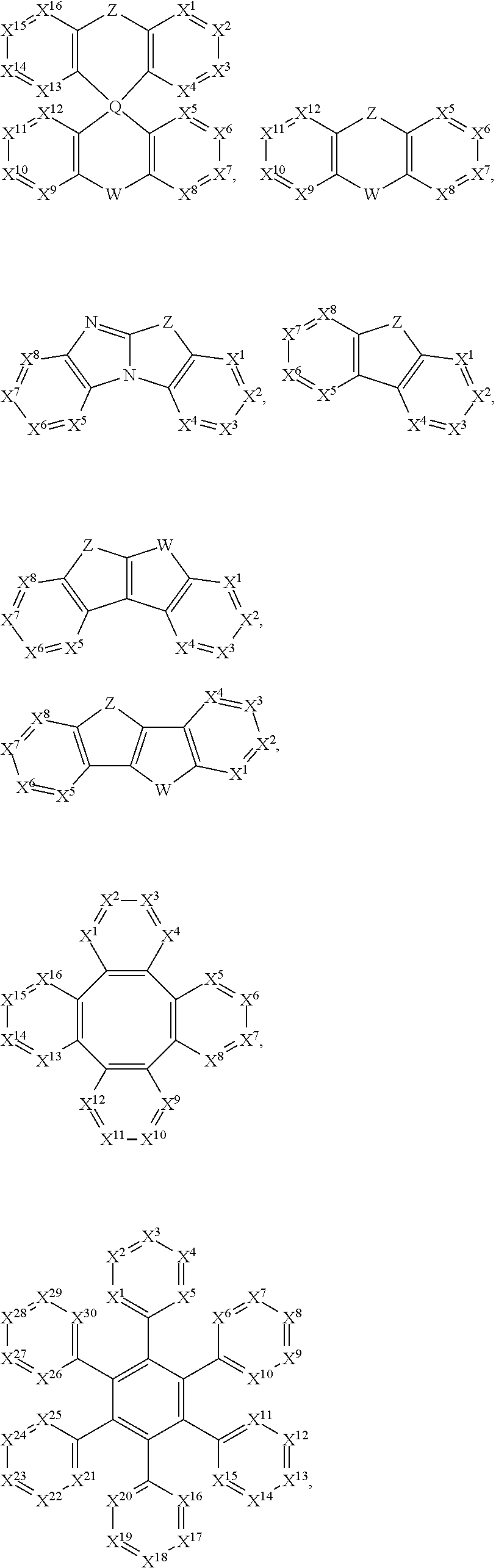

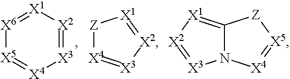
and combinations thereof;

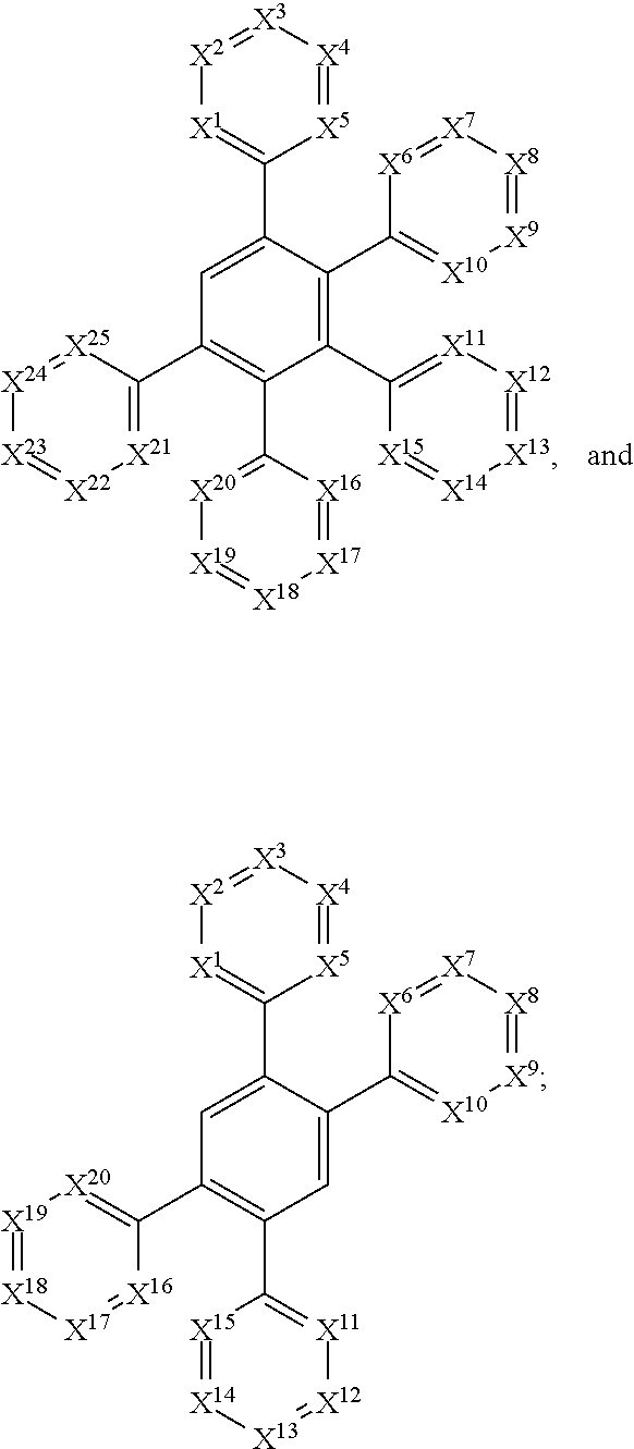
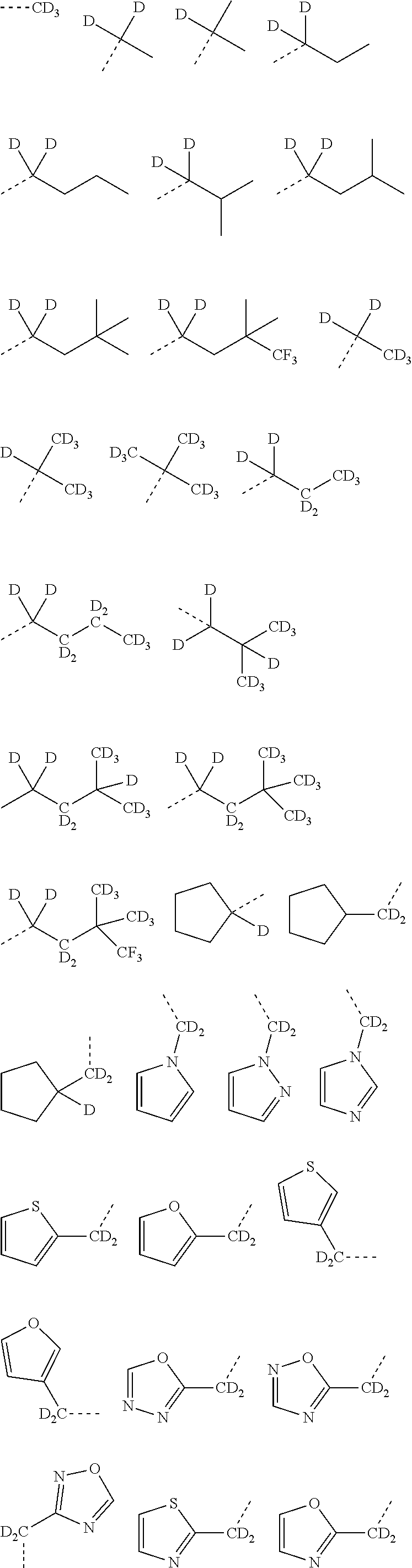

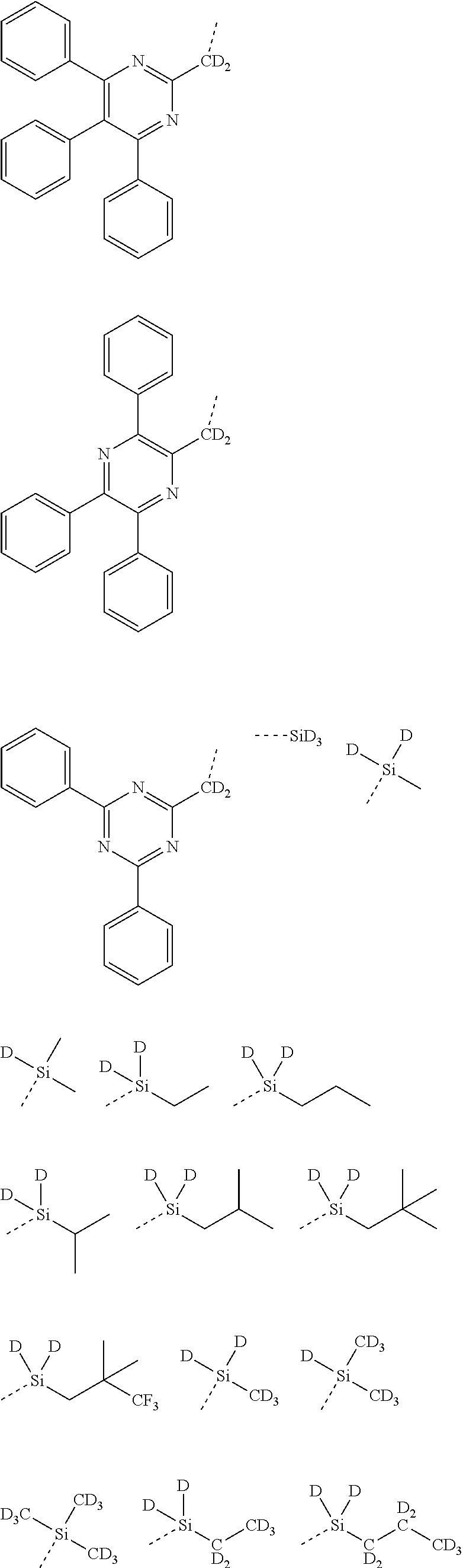


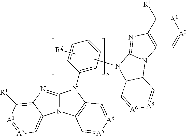
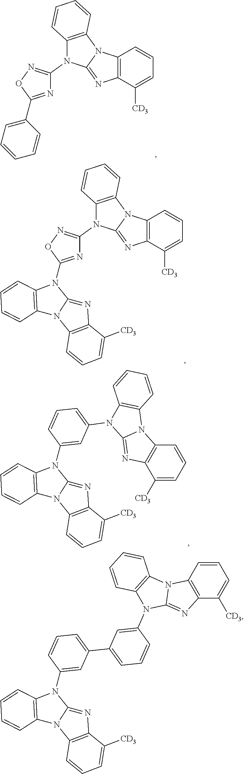
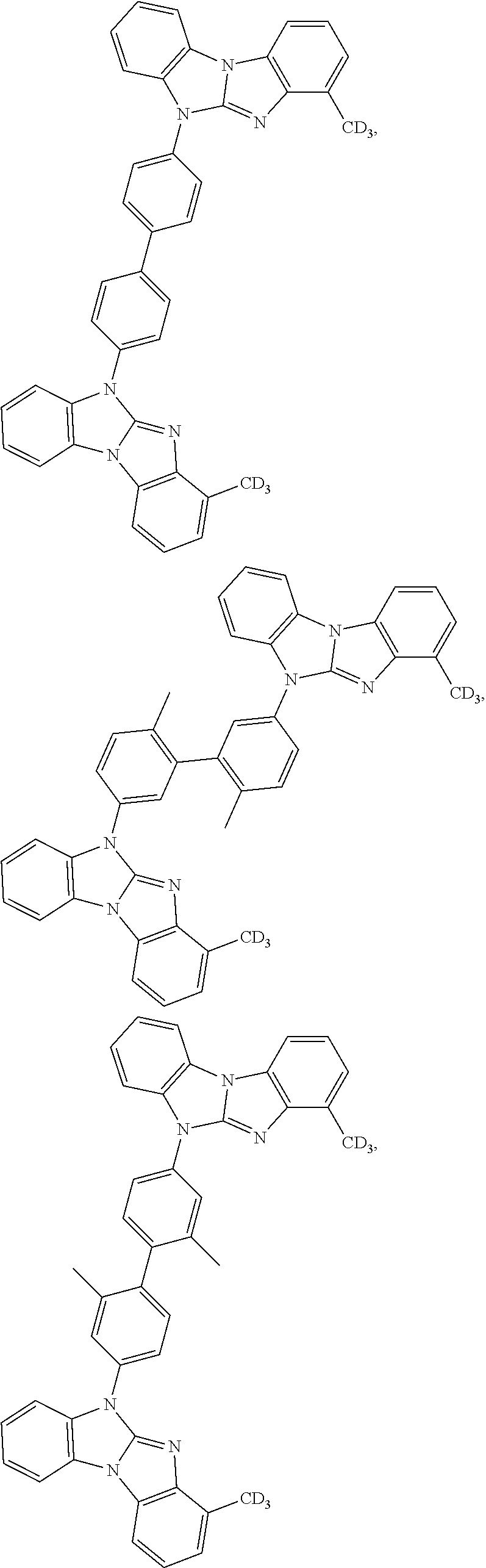
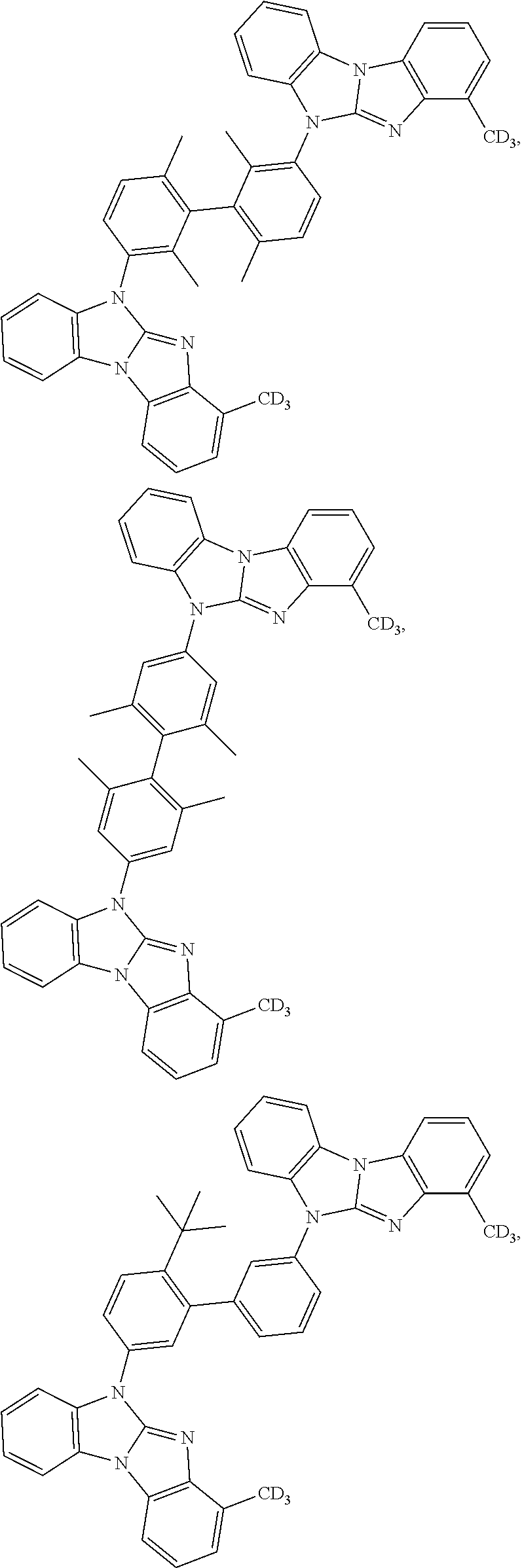
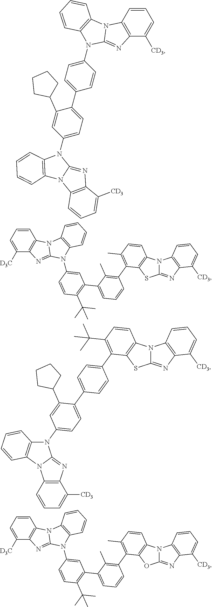
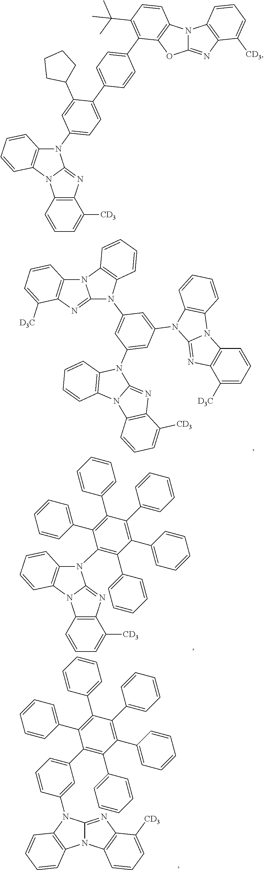

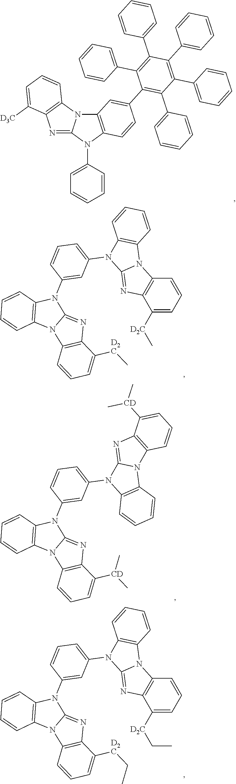

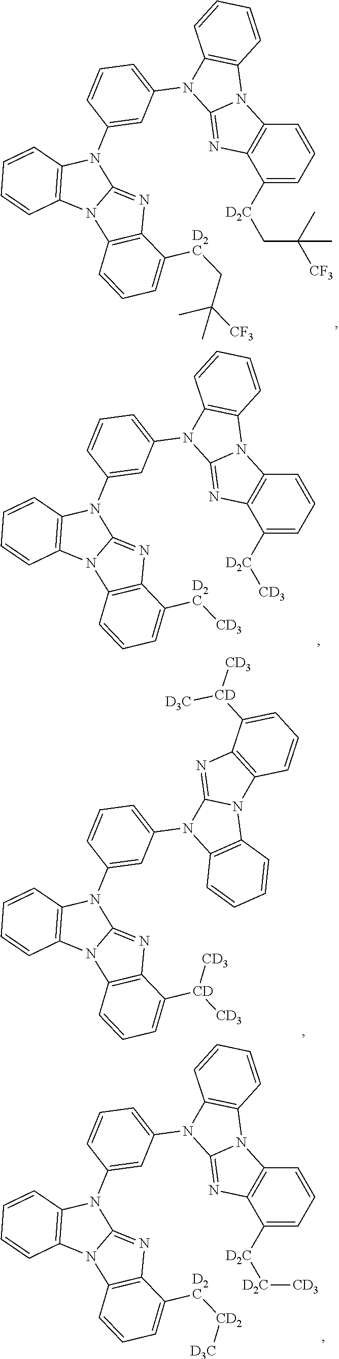
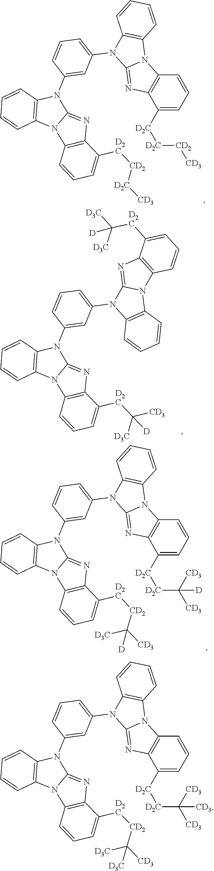
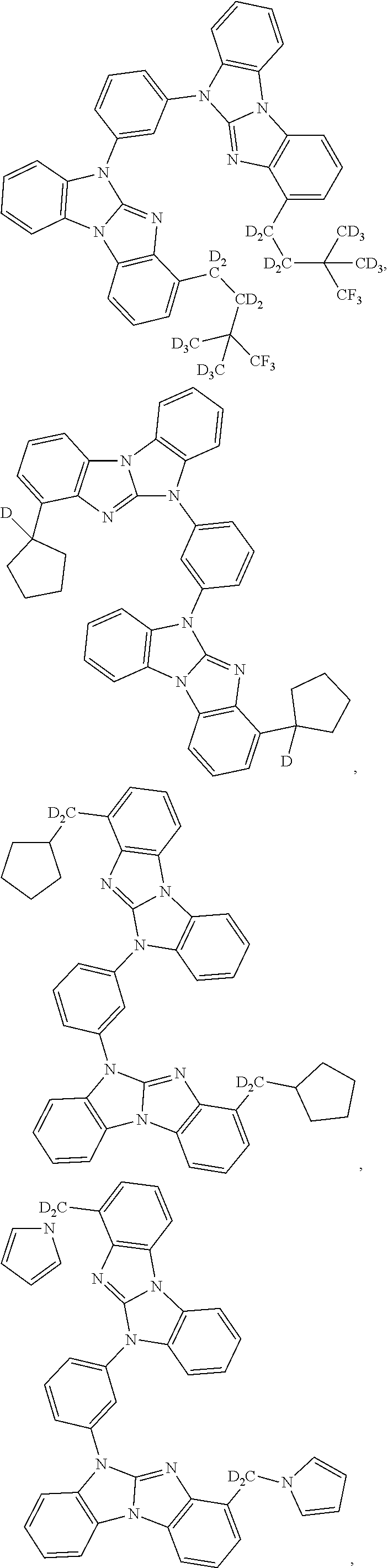


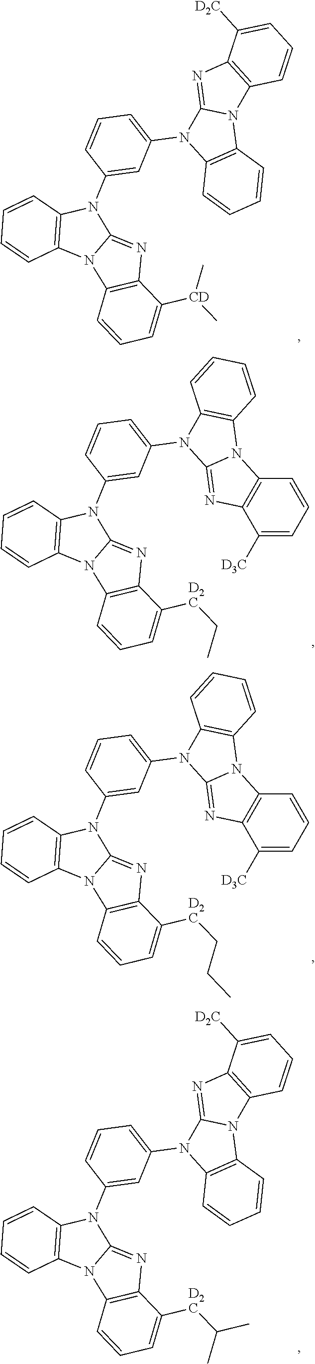
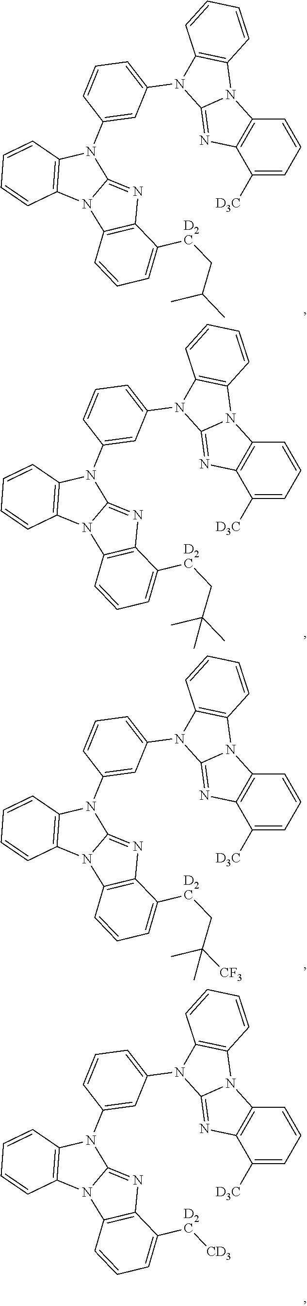

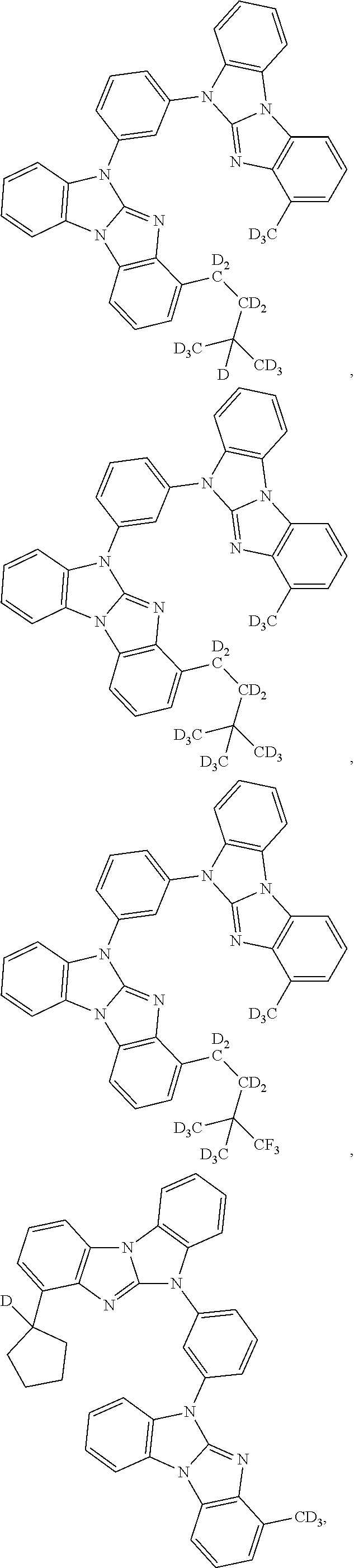


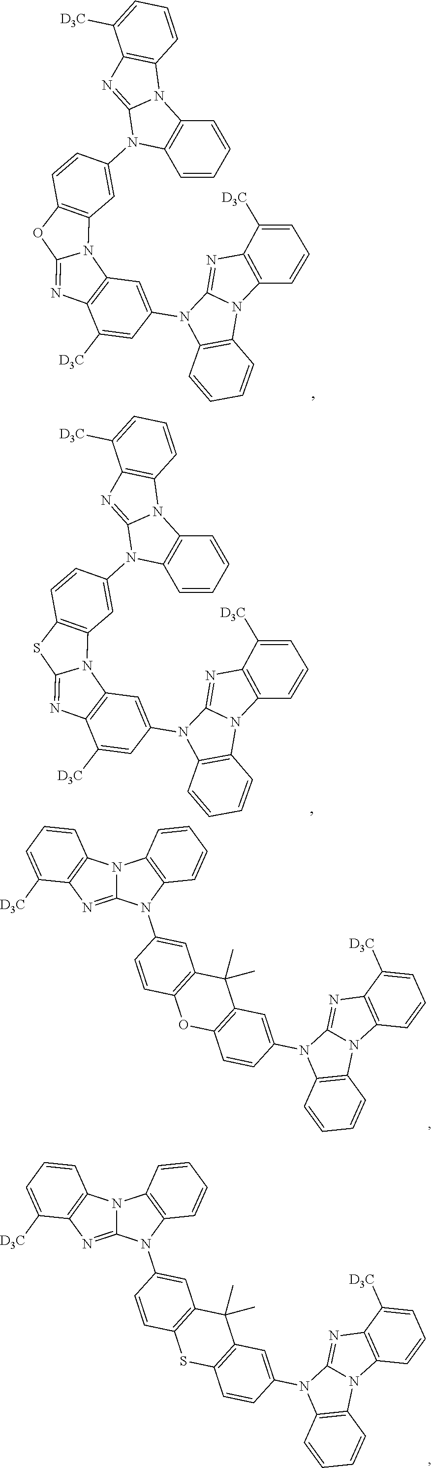
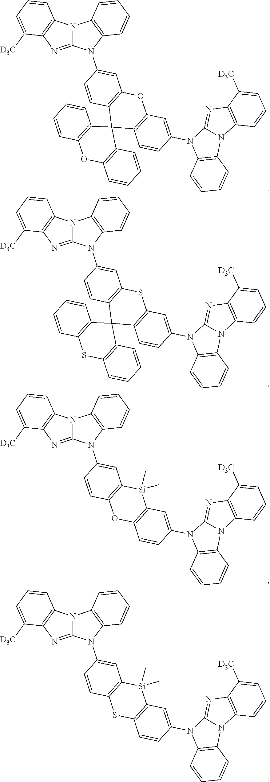


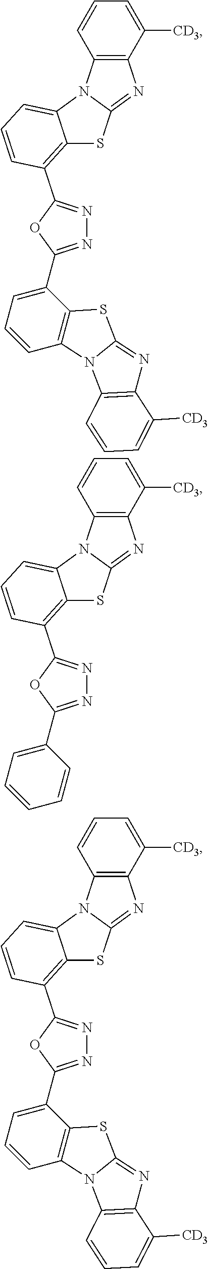
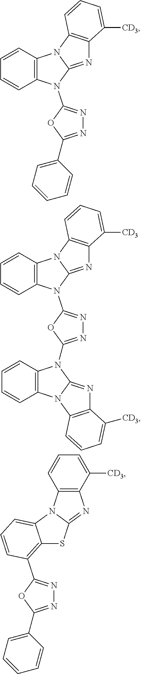
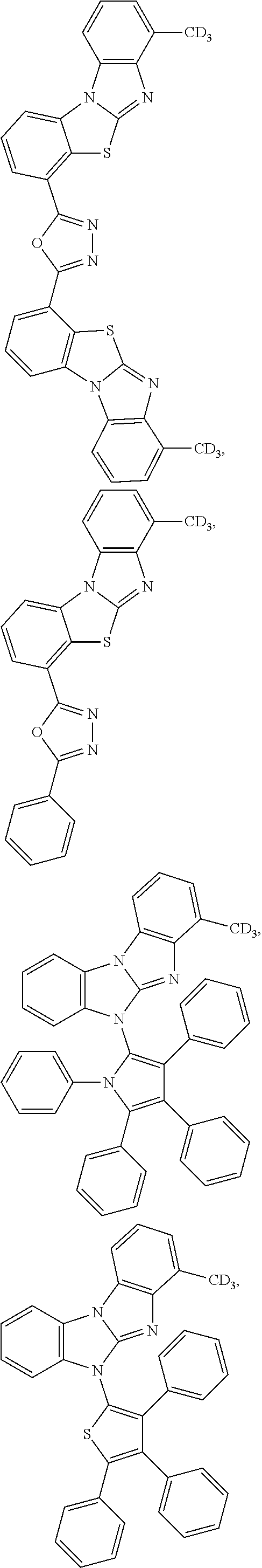


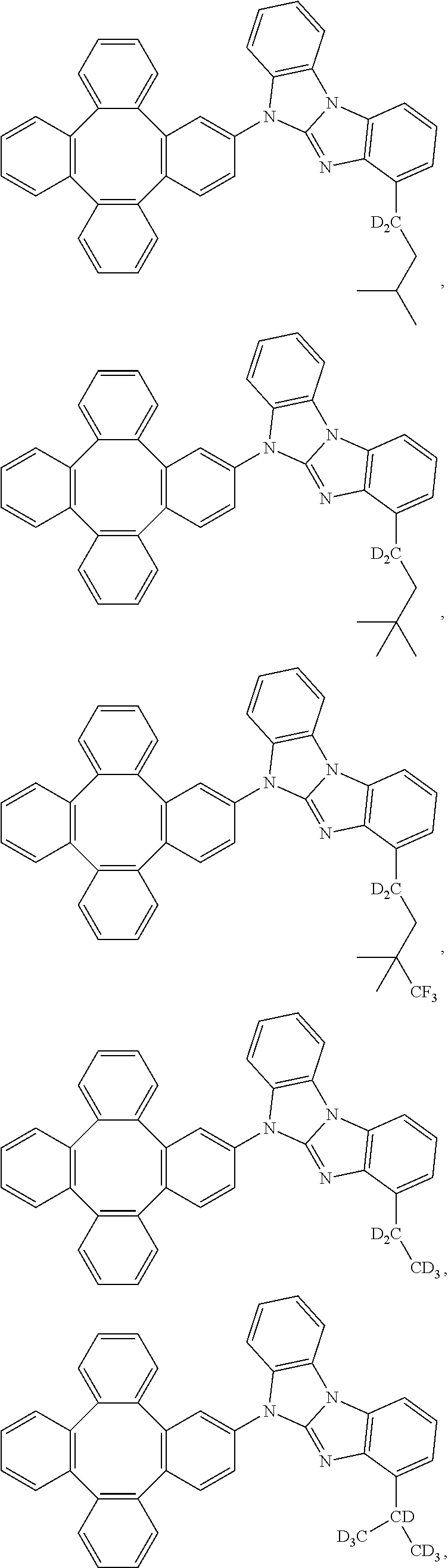
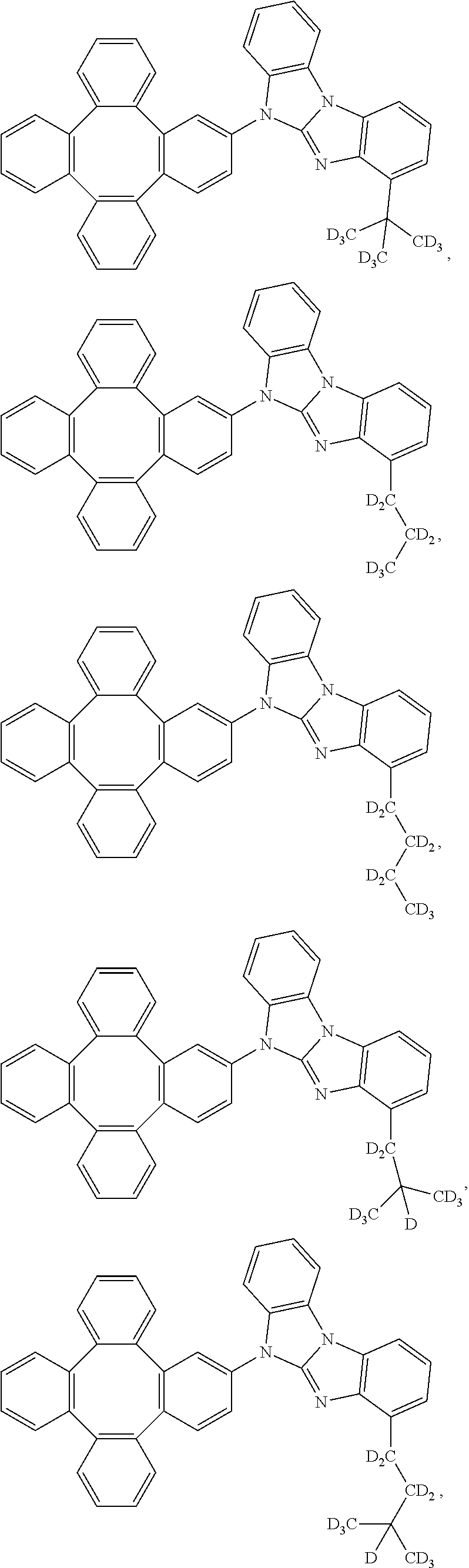


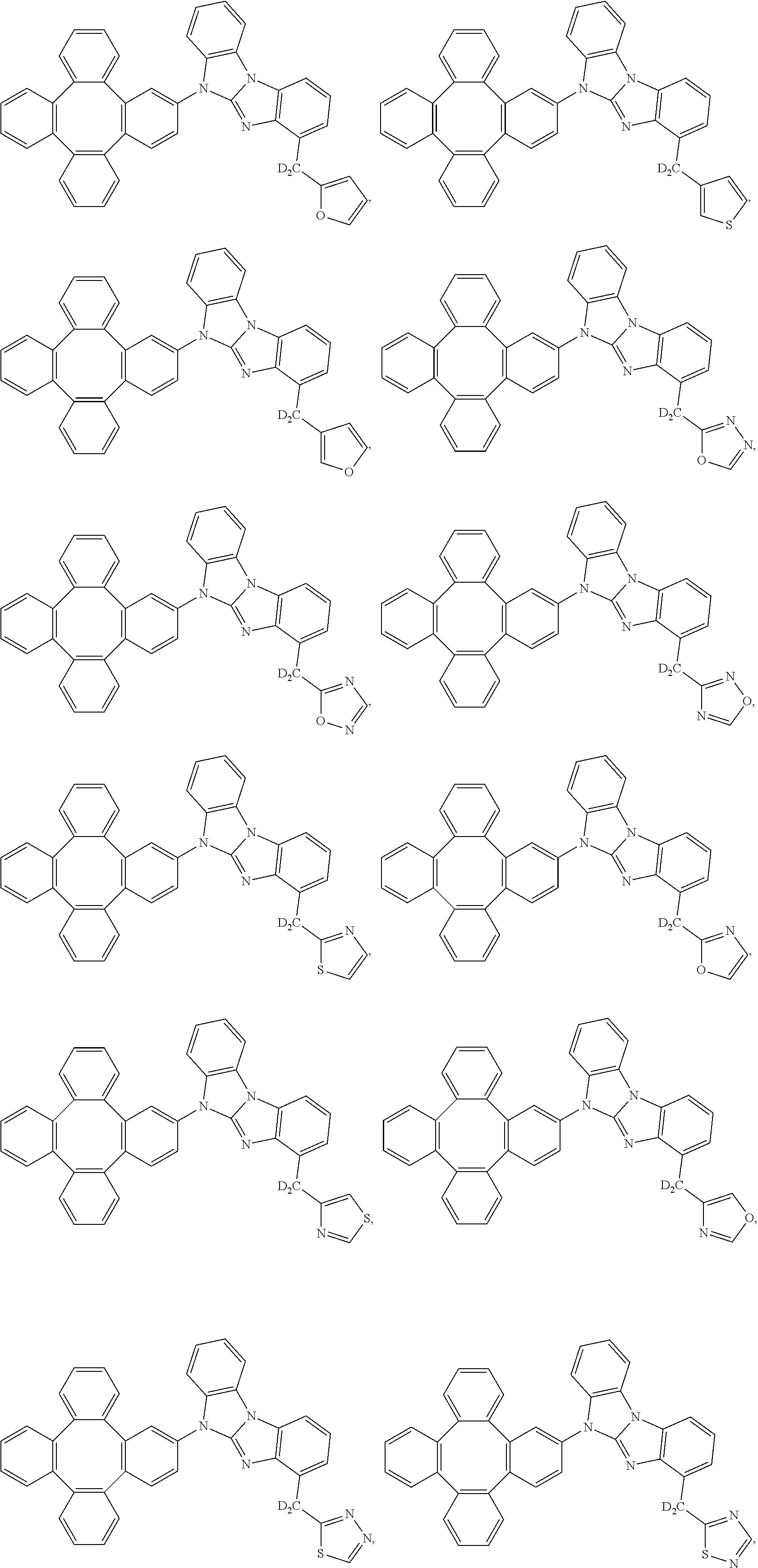
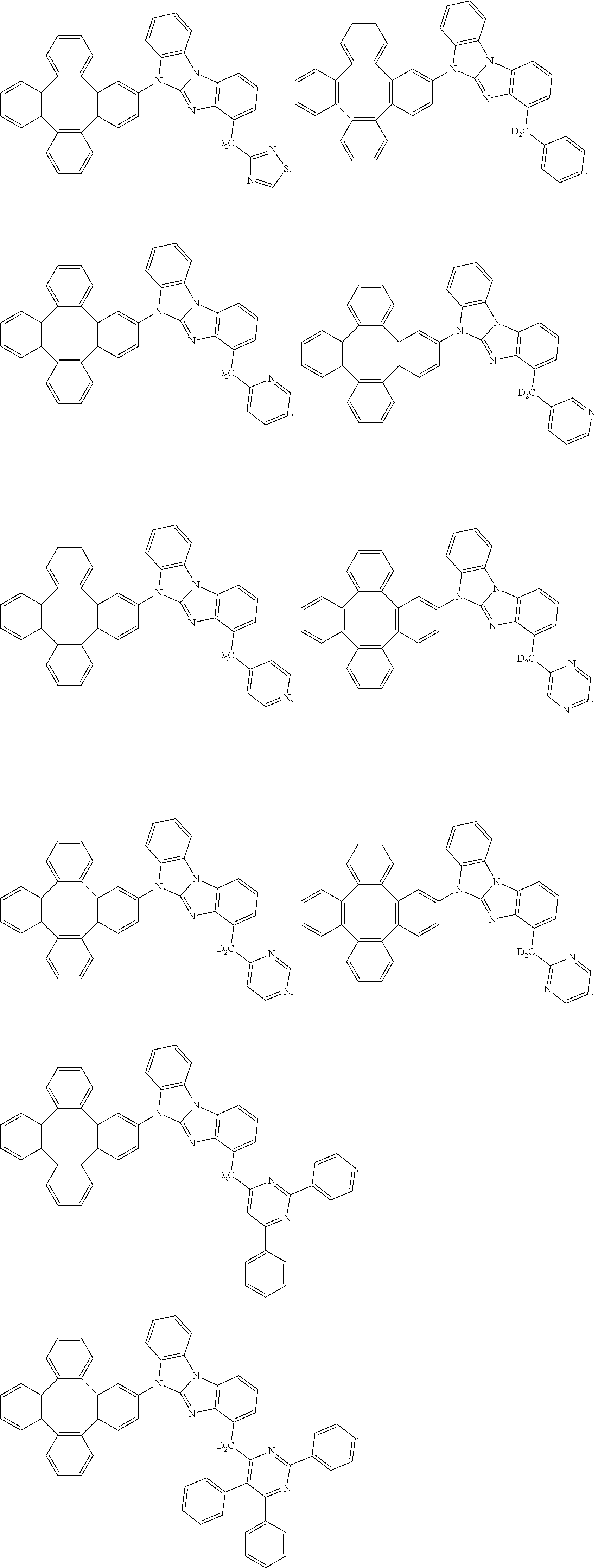

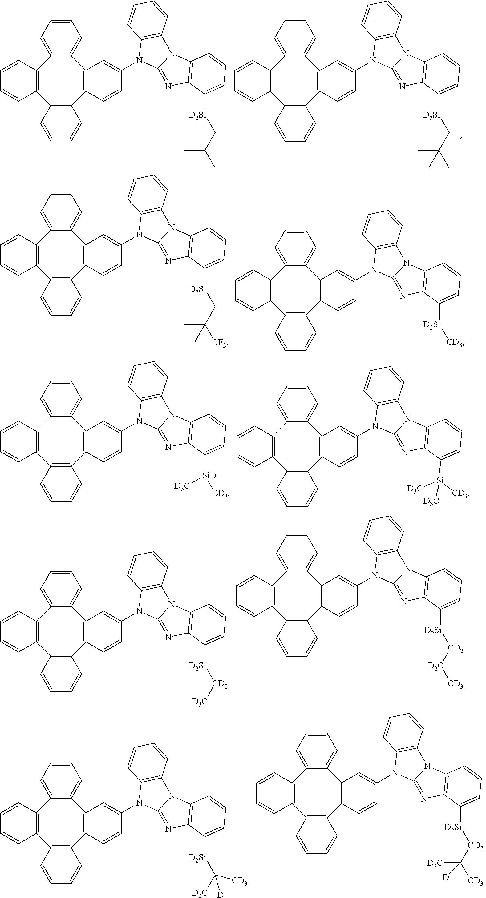

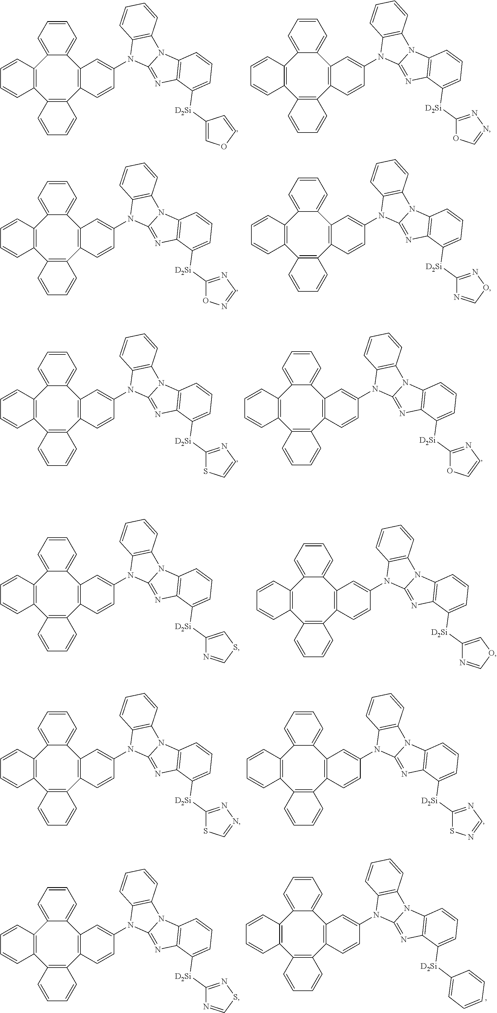
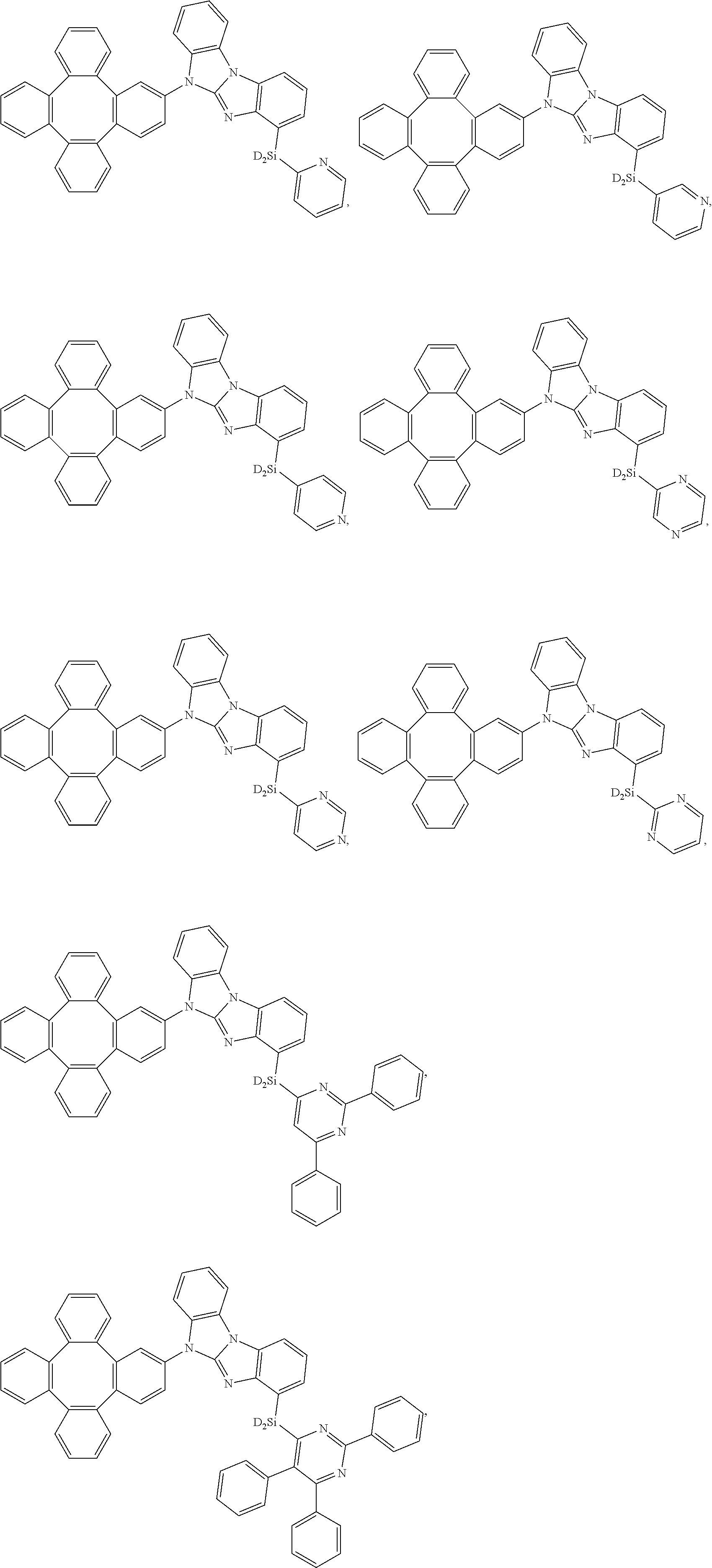

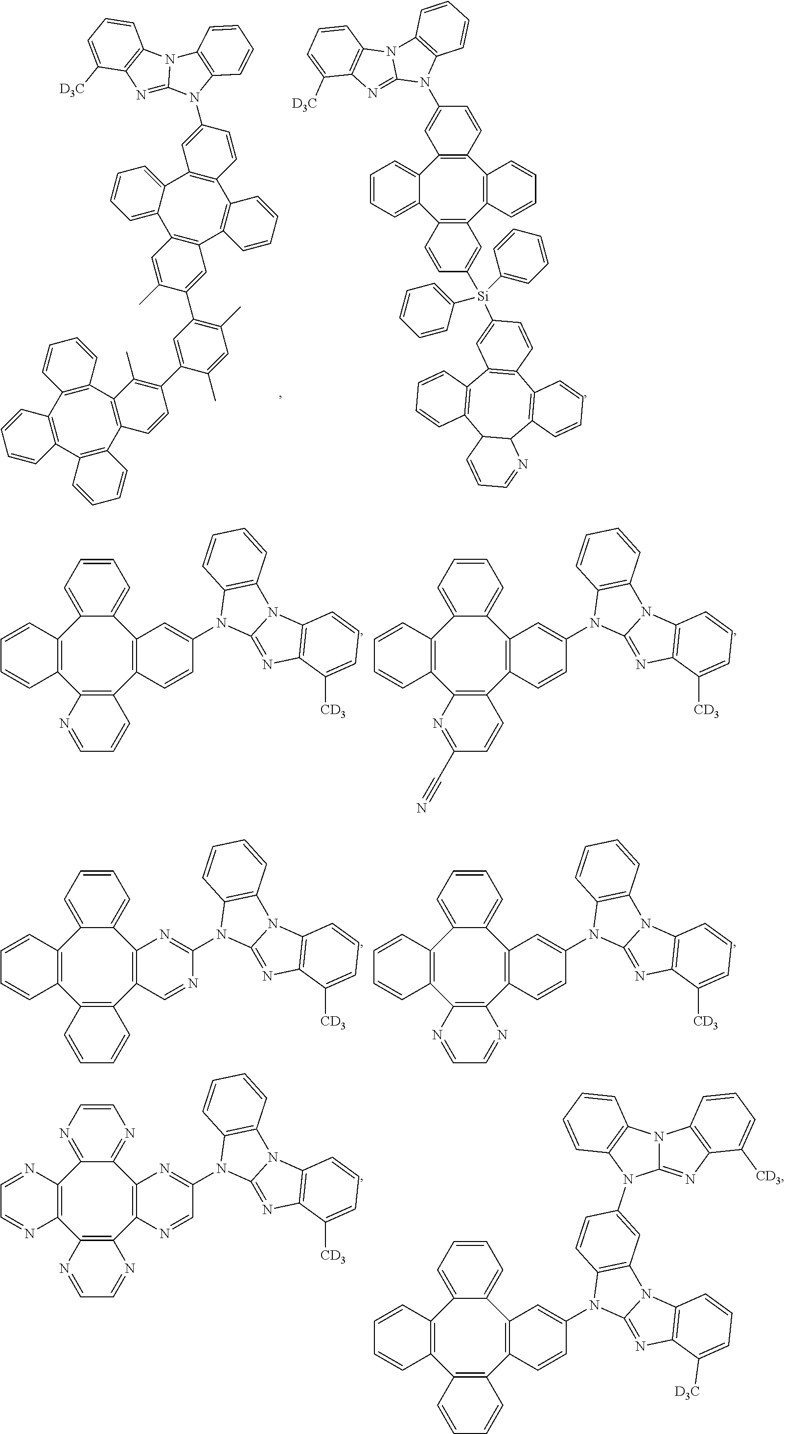

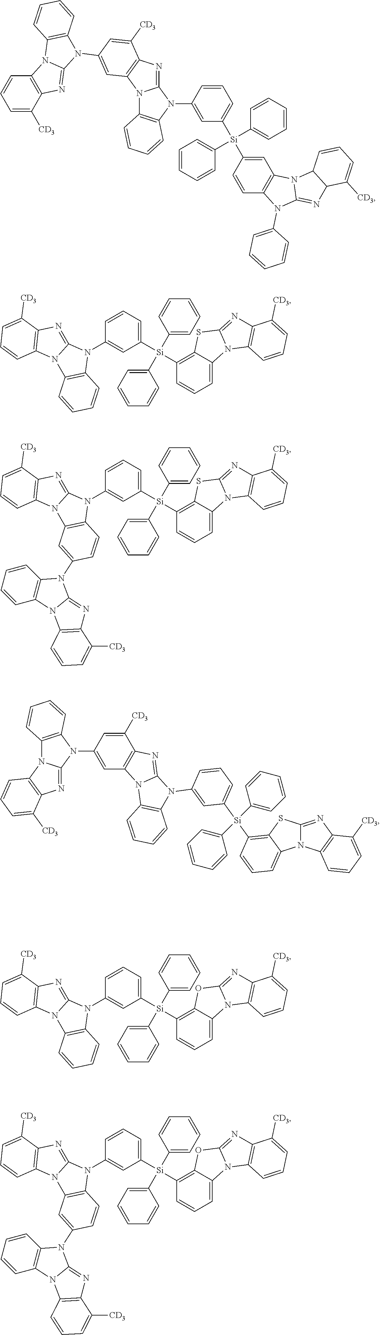


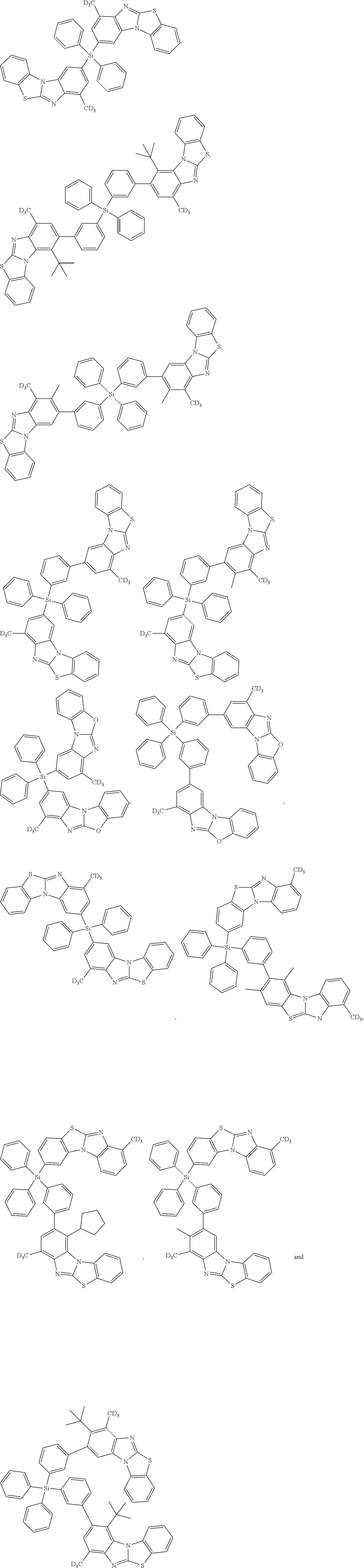

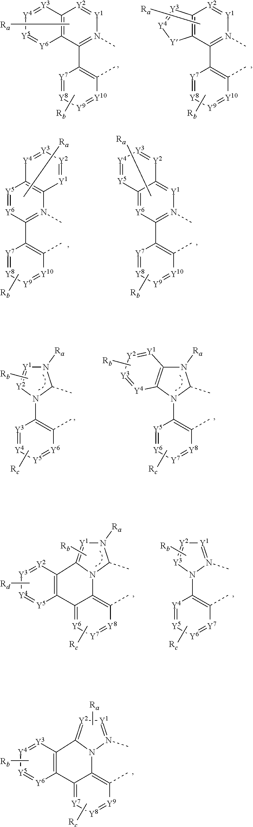
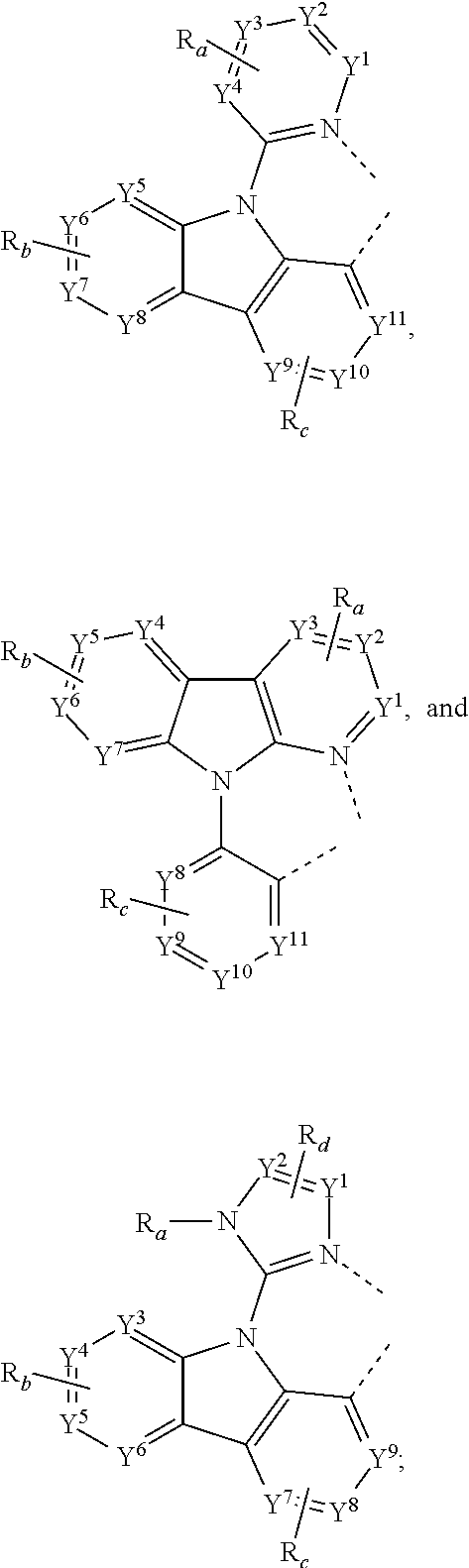
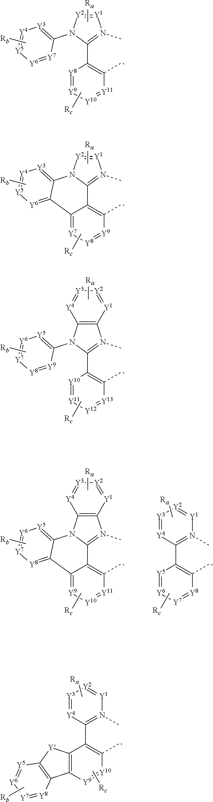


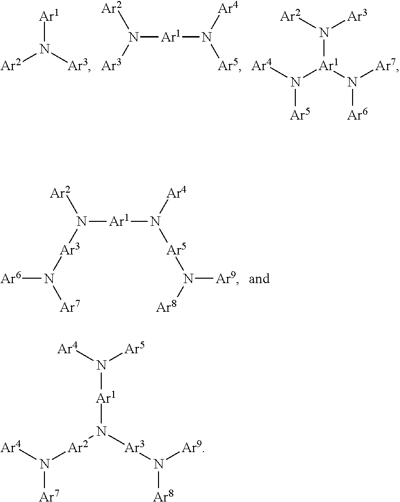

wherein k is an integer from 1 to 20; X101 to X108 is C (including CH) or N; Z101 is NAr1, O, or S; Ar1 has the same group defined above.
wherein Met is a metal, which can have an atomic weight greater than 40; (Y101-Y102)) is a bidentate ligand, Y101 and Y102 are independently selected from C, N, O, P, and S; L101 is an ancillary ligand; k′ is an integer value from 1 to the maximum number of ligands that may be attached to the metal; and k′+k″ is the maximum number of ligands that may be attached to the metal.


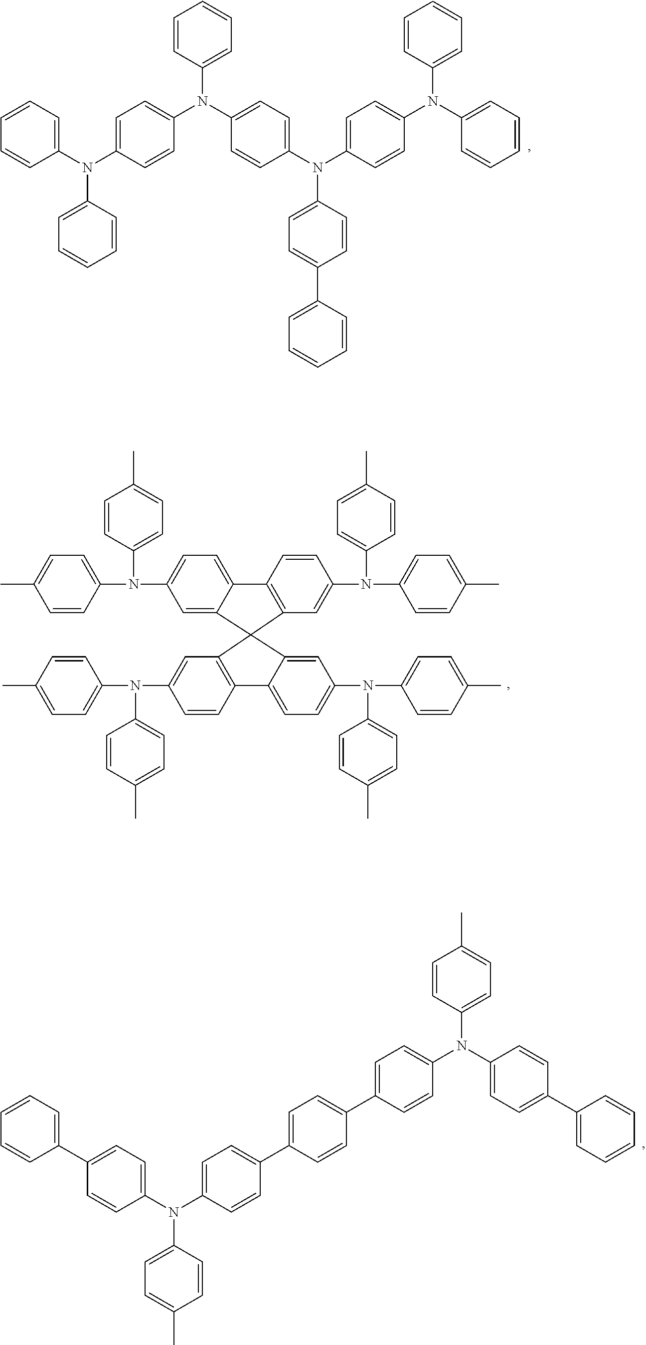


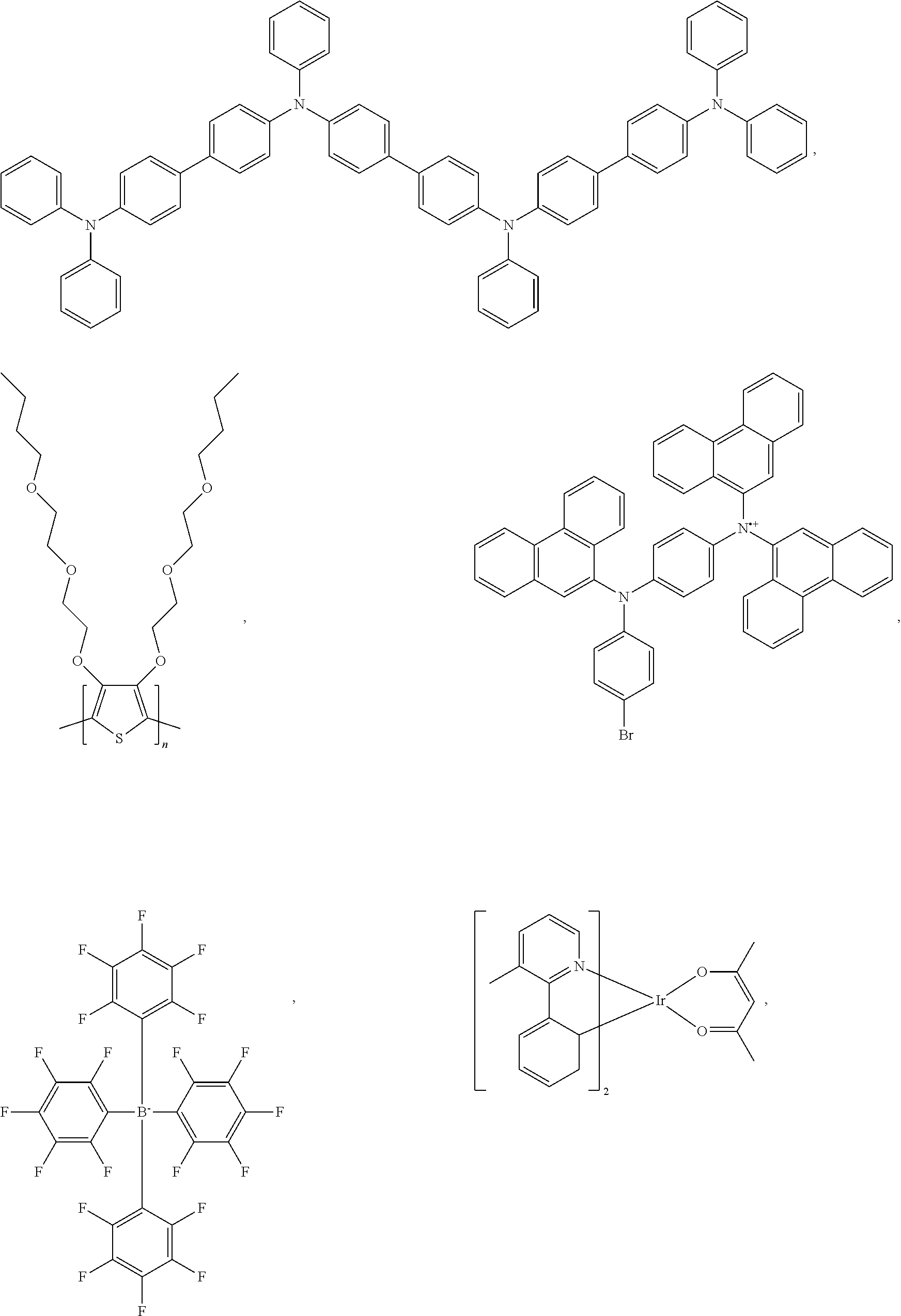

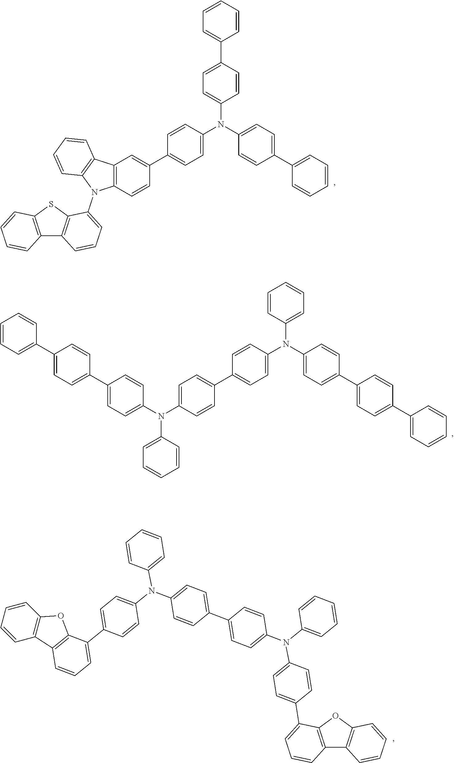


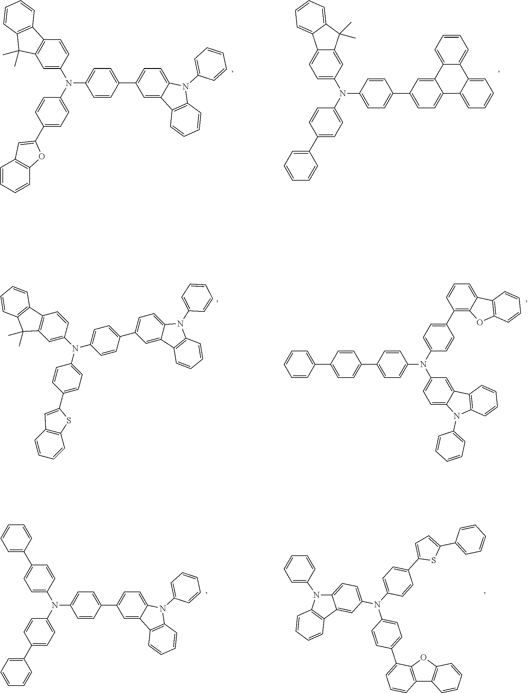
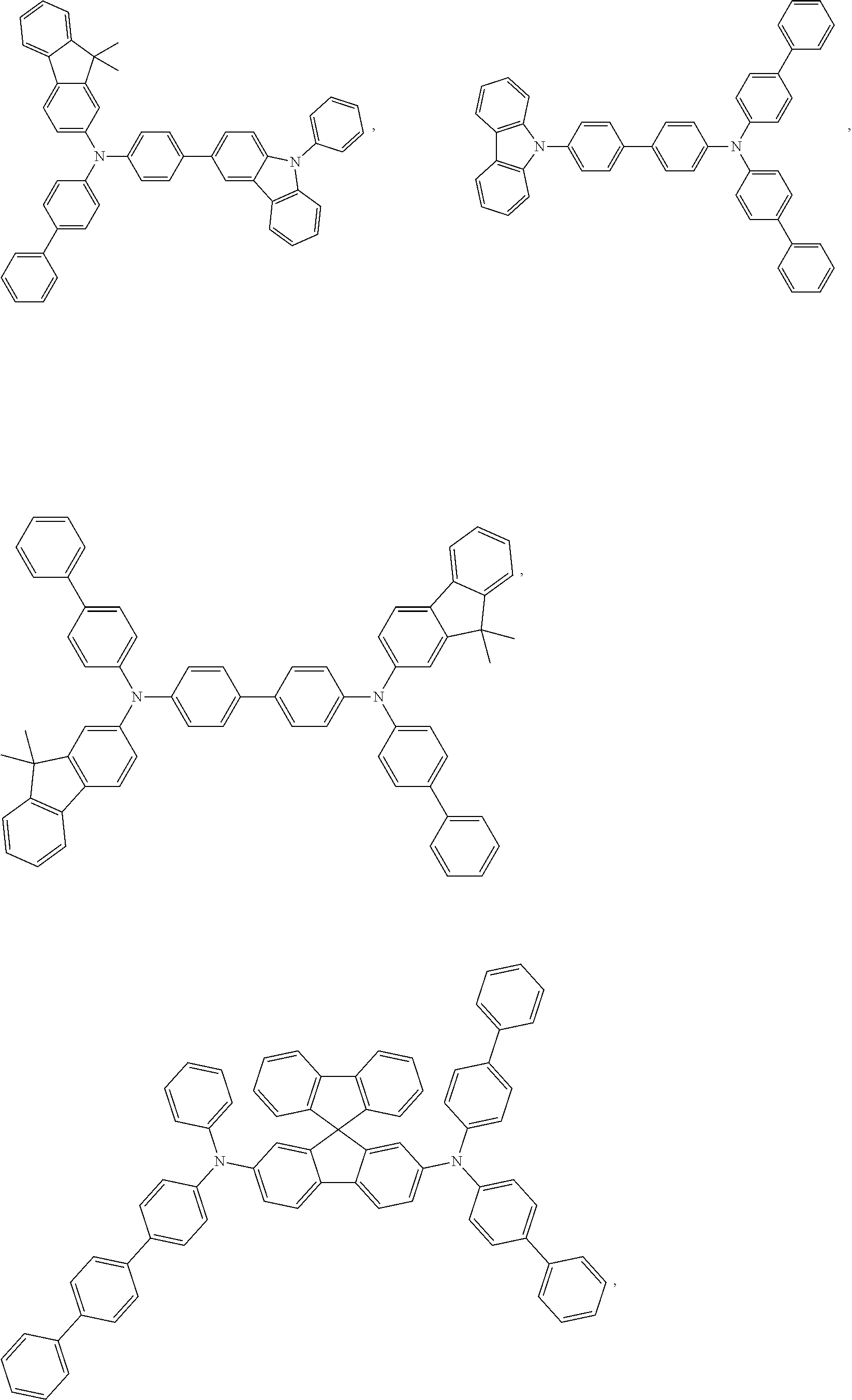


wherein Met is a metal; (Y103-Y104) is a bidentate ligand, Y103 and Y104 are independently selected from C, N, O, P, and S; L101 is an another ligand; k′ is an integer value from 1 to the maximum number of ligands that may be attached to the metal; and k′+k″ is the maximum number of ligands that may be attached to the metal.
wherein (O—N) is a bidentate ligand, having metal coordinated to atoms O and N.
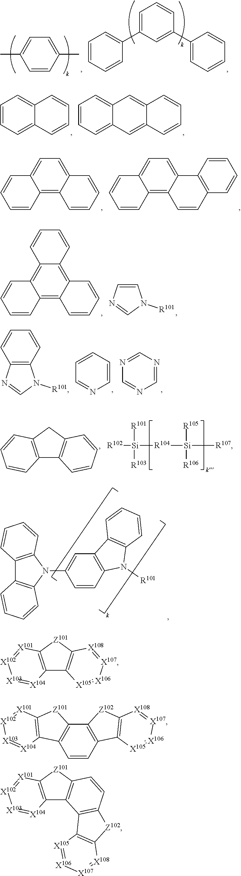

wherein each of R101 to R107 is independently selected from the group consisting of hydrogen, deuterium, halide, alkyl, cycloalkyl, heteroalkyl, arylalkyl, alkoxy, aryloxy, amino, silyl, alkenyl, cycloalkenyl, heteroalkenyl, alkynyl, aryl, heteroaryl, acyl, carbonyl, carboxylic acids, ester, nitrile, isonitrile, sulfanyl, sulfinyl, sulfonyl, phosphino, and combinations thereof, and when it is aryl or heteroaryl, it has the similar definition as Ar's mentioned above. k is an integer from 0 to 20 or 1 to 20; k′″ is an integer from 0 to 20. X101 to X108 is selected from C (including CH) or N. Z101 and Z102 is selected from NR101, O, or S.


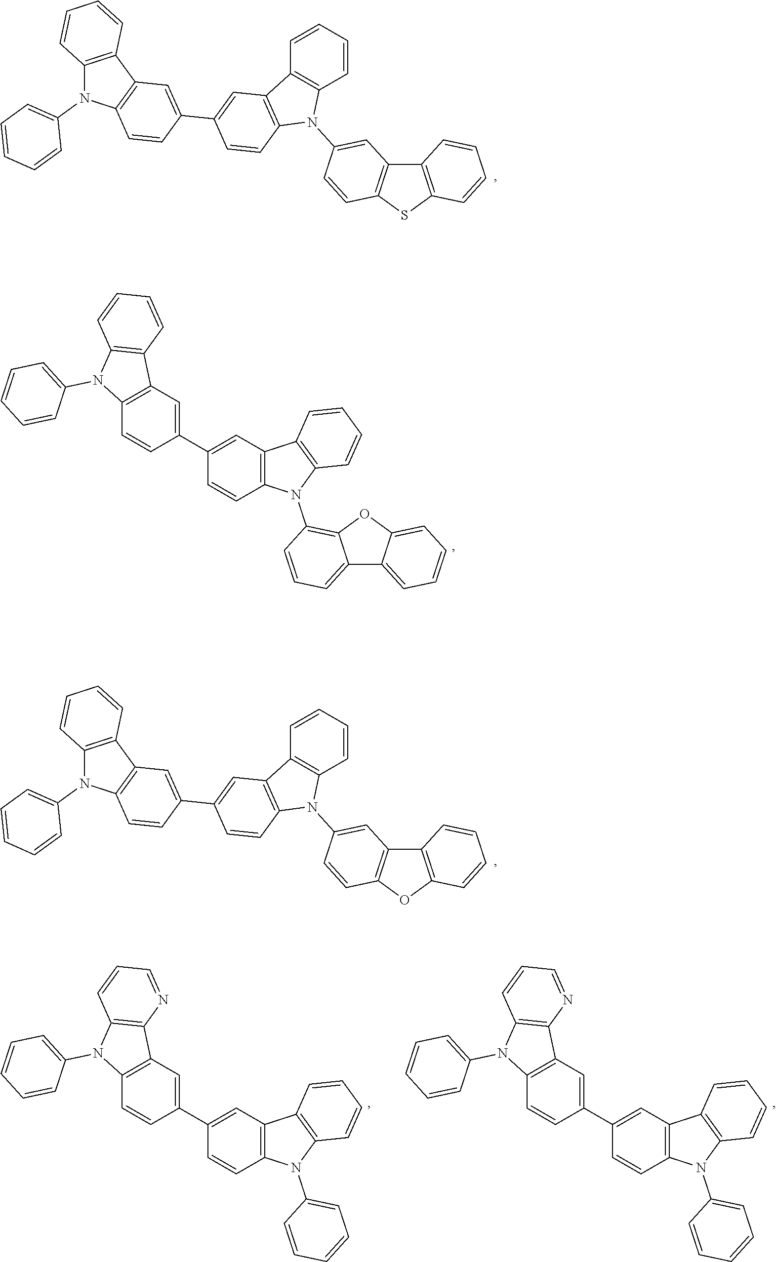


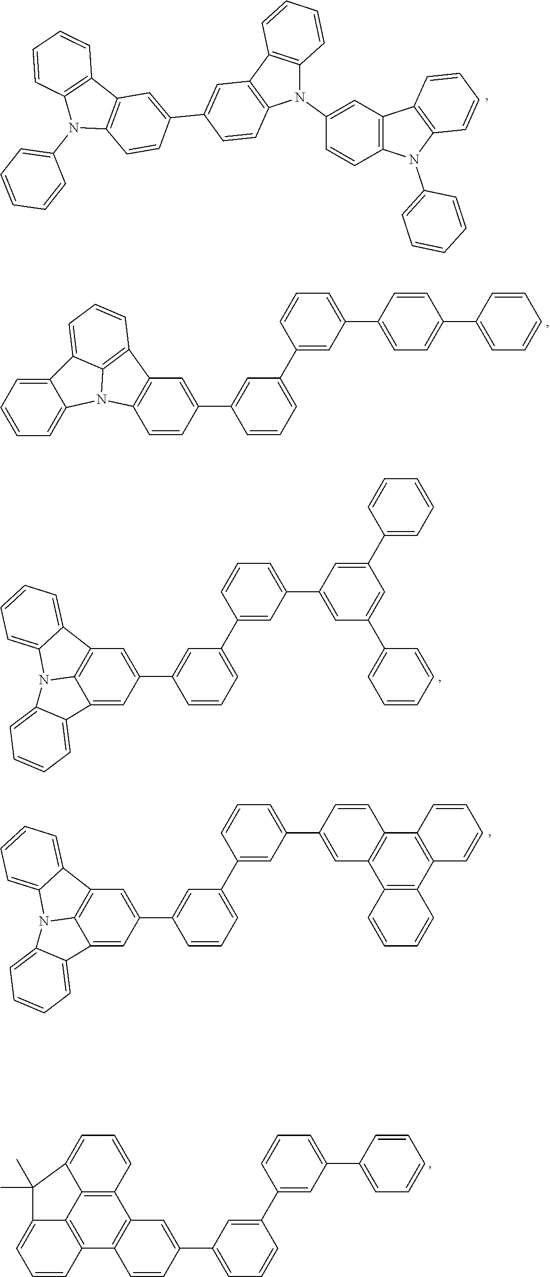

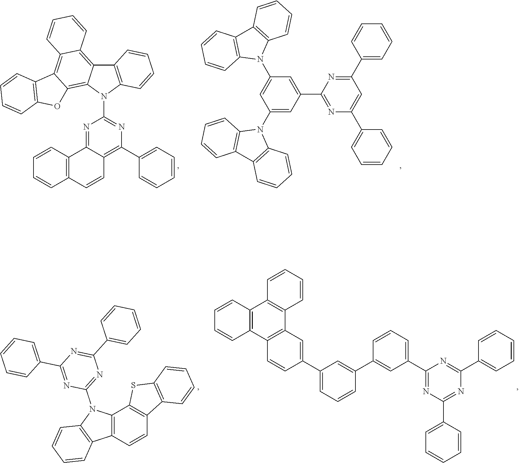


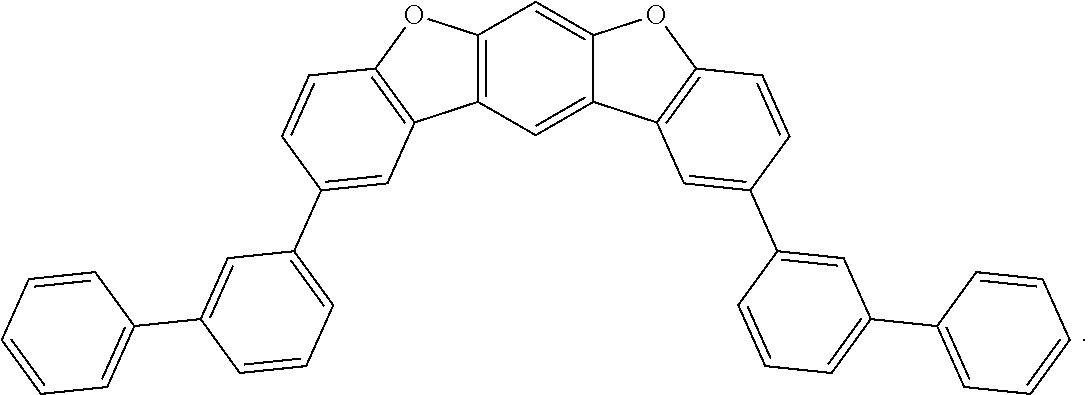
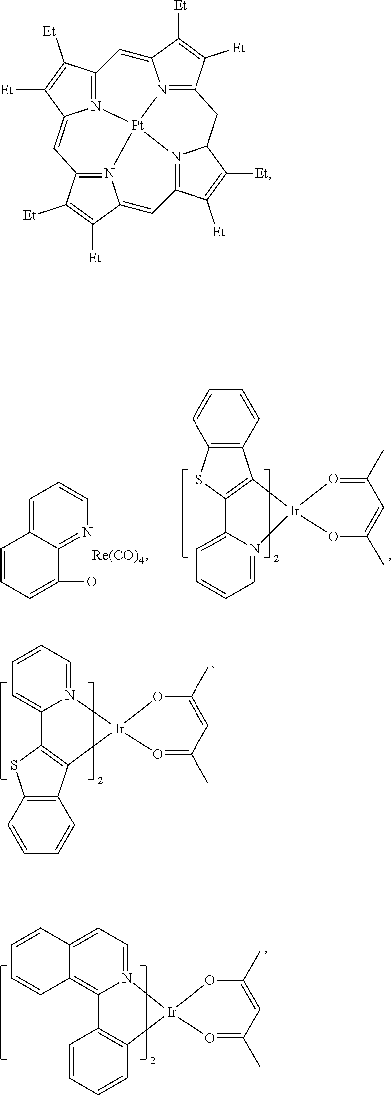
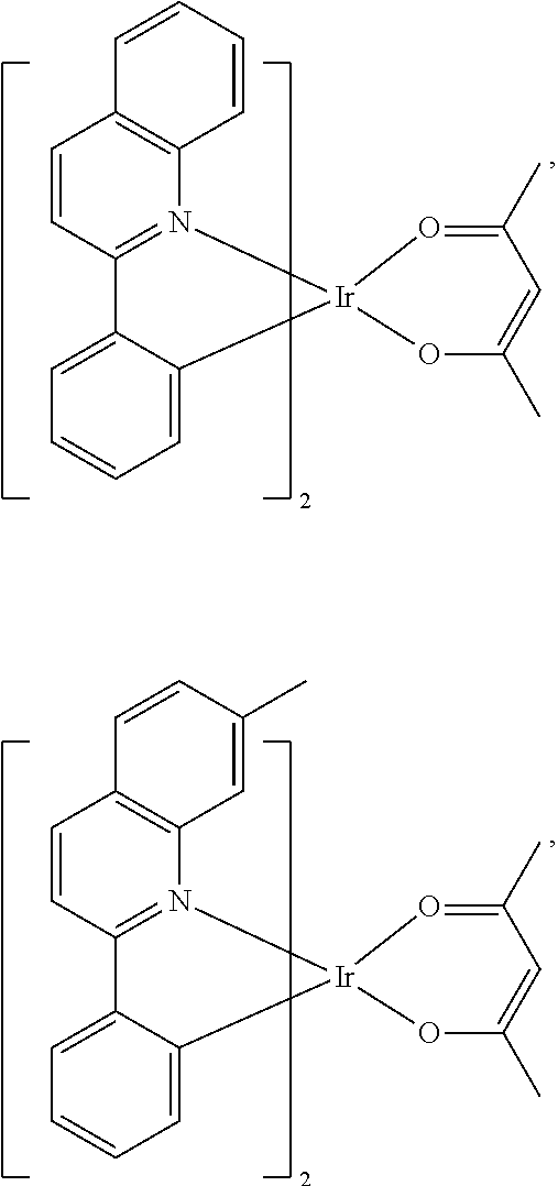
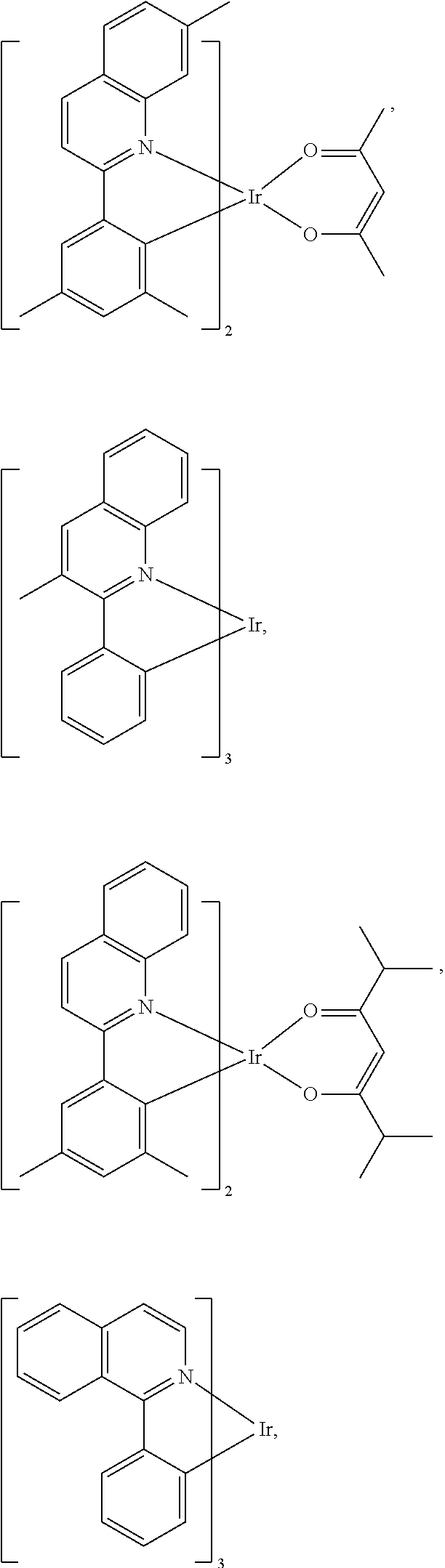


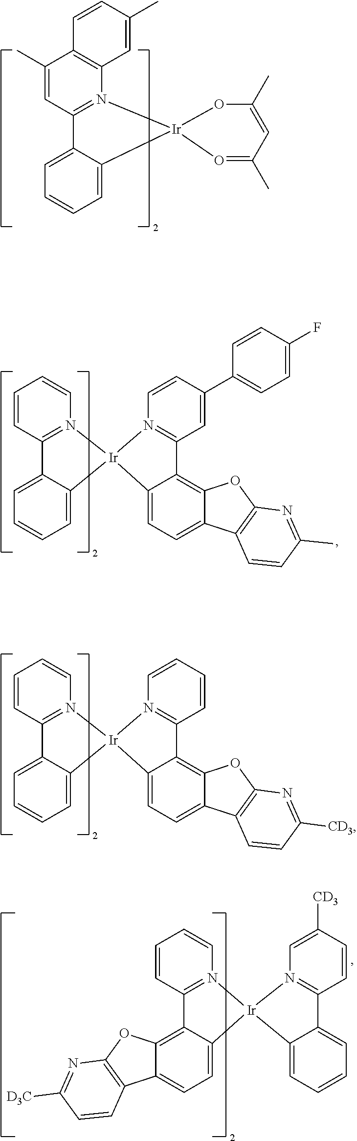
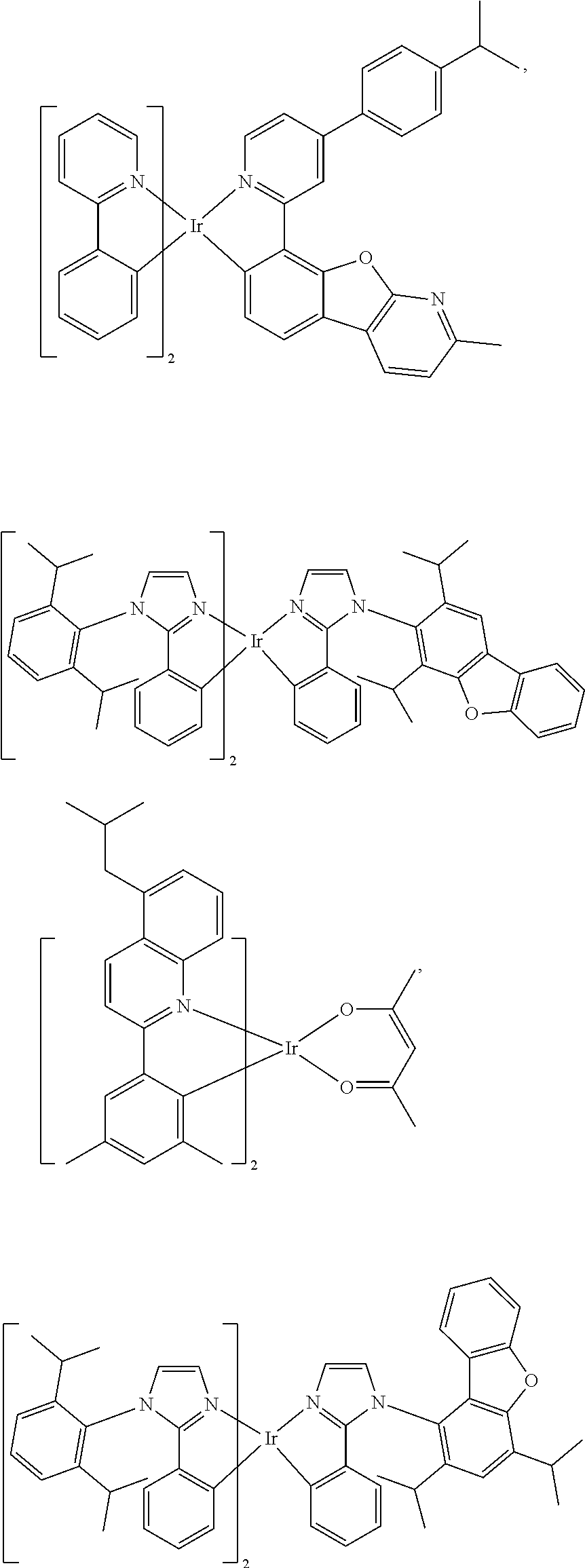

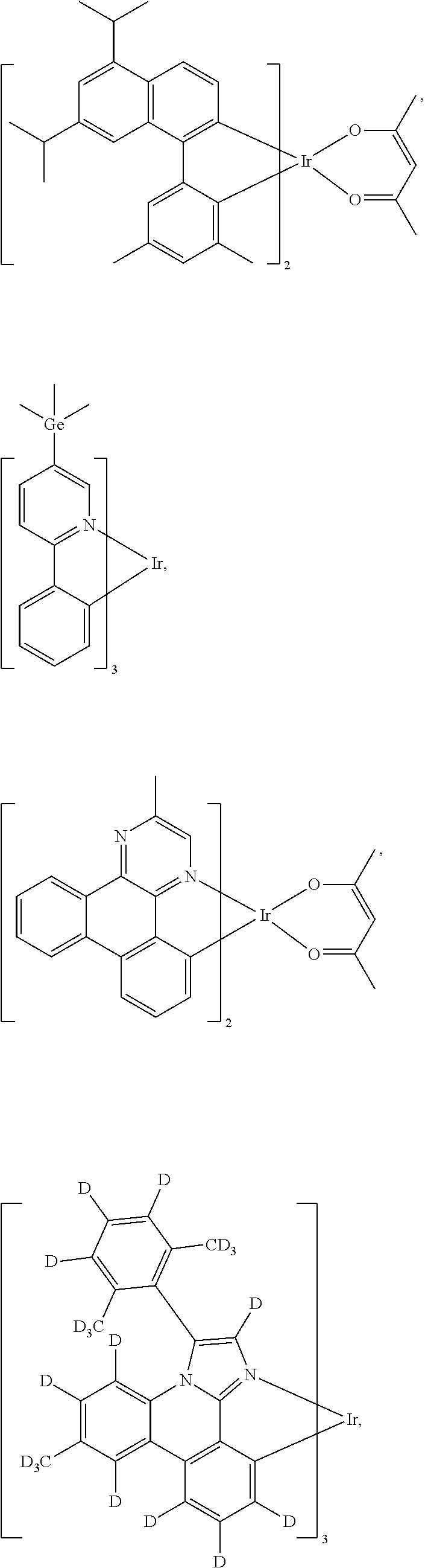


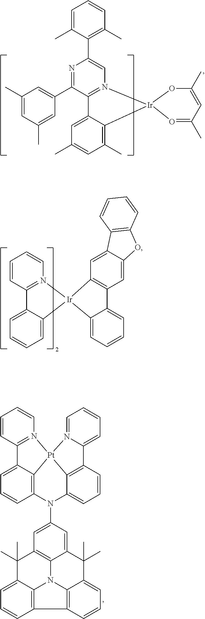


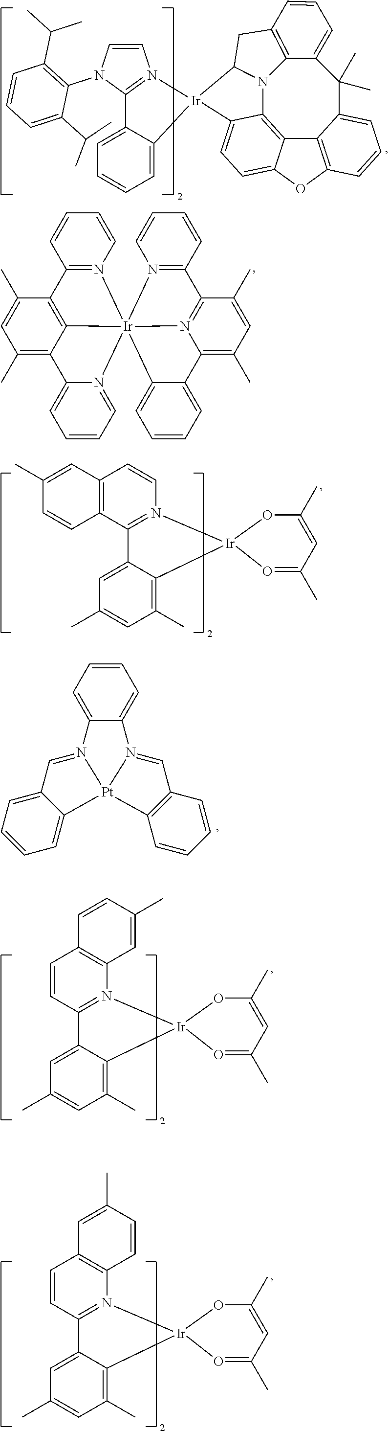

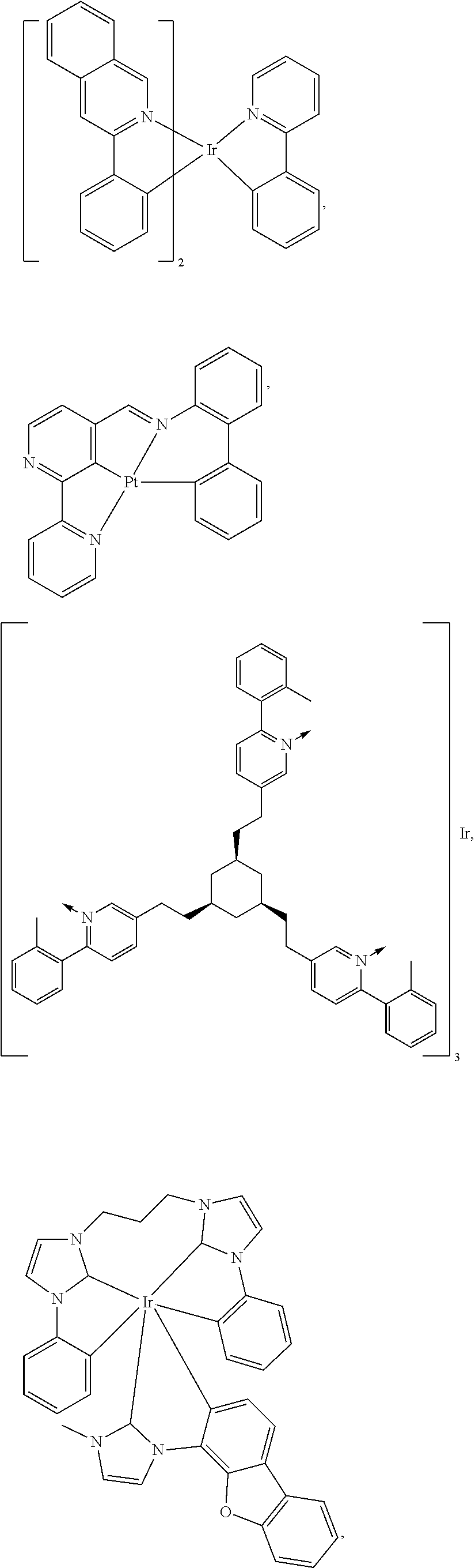

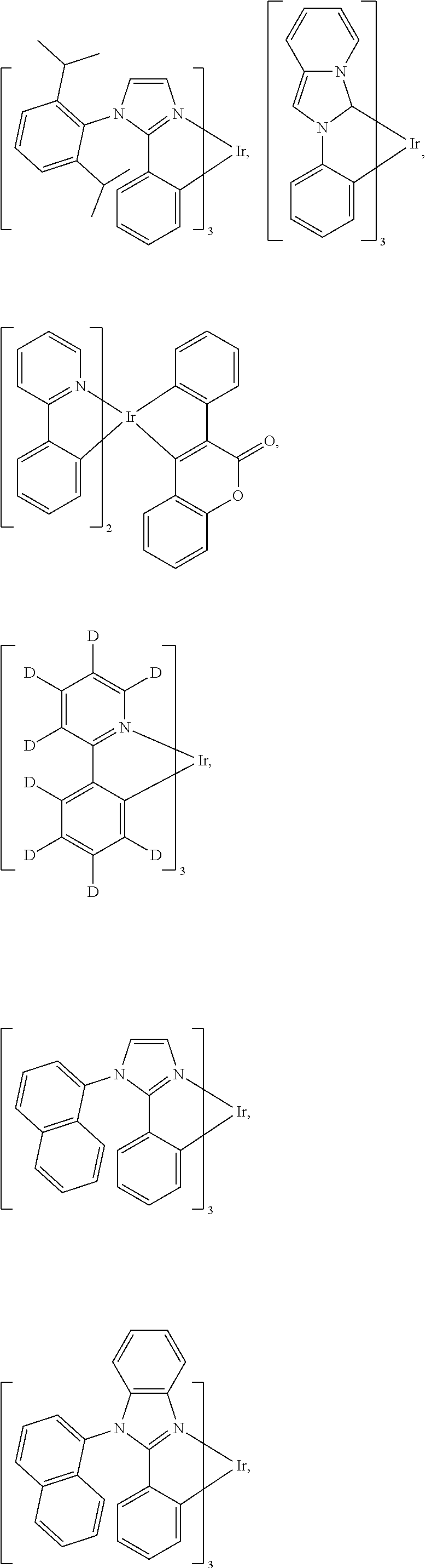
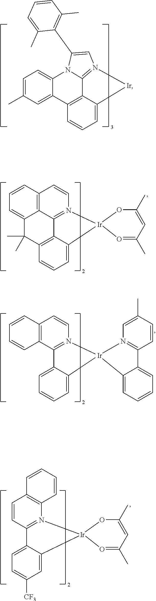
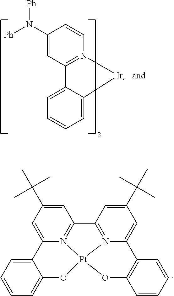
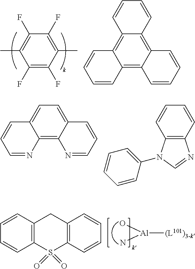
wherein k is an integer from 1 to 20; L101 is an another ligand, k′ is an integer from 1 to 3.
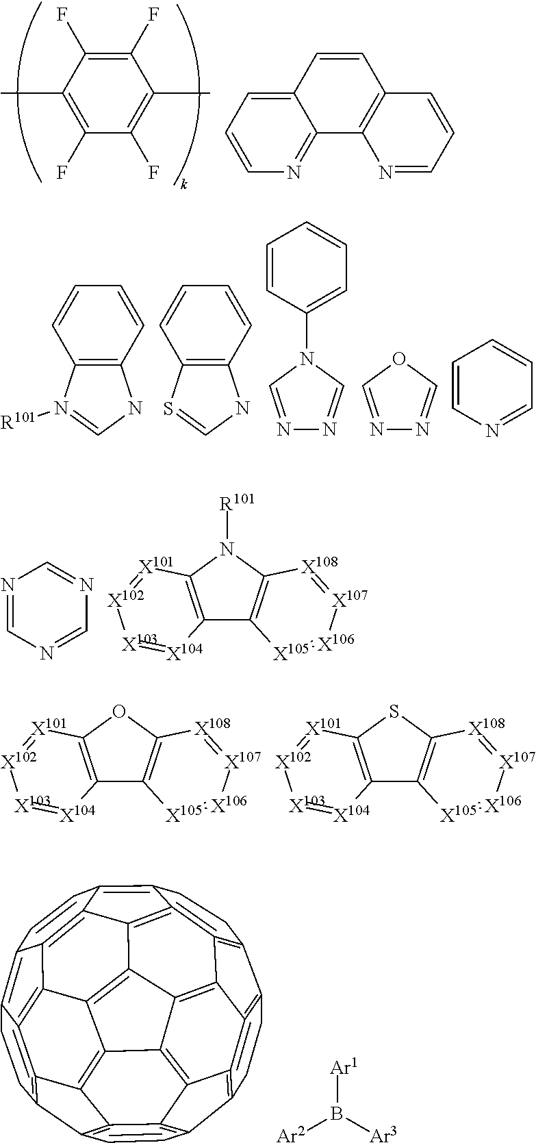
wherein R101 is selected from the group consisting of hydrogen, deuterium, halide, alkyl, cycloalkyl, heteroalkyl, arylalkyl, alkoxy, aryloxy, amino, silyl, alkenyl, cycloalkenyl, heteroalkenyl, alkynyl, aryl, heteroaryl, acyl, carbonyl, carboxylic acids, ester, nitrile, isonitrile, sulfanyl, sulfinyl, sulfonyl, phosphino, and combinations thereof, when it is aryl or heteroaryl, it has the similar definition as Ar's mentioned above. Ar1 to Ar3 has the similar definition as Ar's mentioned above. k is an integer from 1 to 20. X101 to X108 is selected from C (including CH) or N.
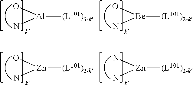
wherein (O—N) or (N—N) is a bidentate ligand, having metal coordinated to atoms O, N or N, N; L101 is another ligand; k′ is an integer value from 1 to the maximum number of ligands that may be attached to the metal.
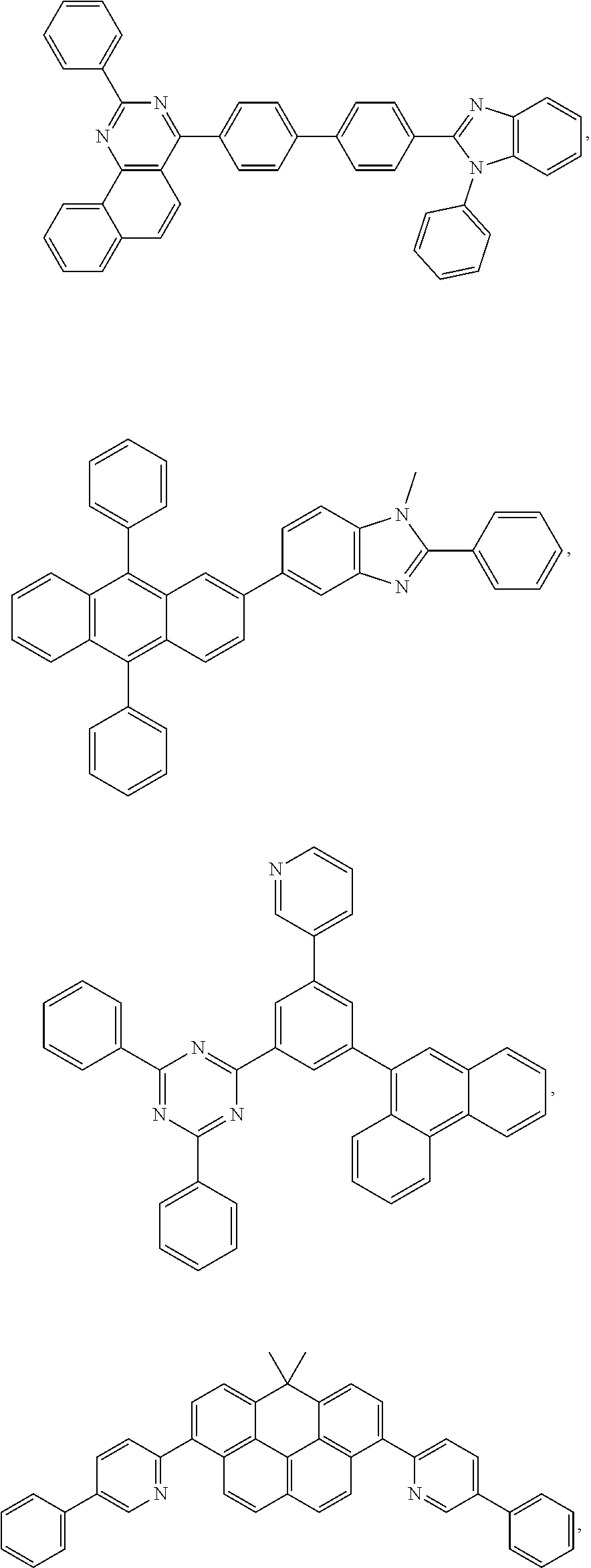
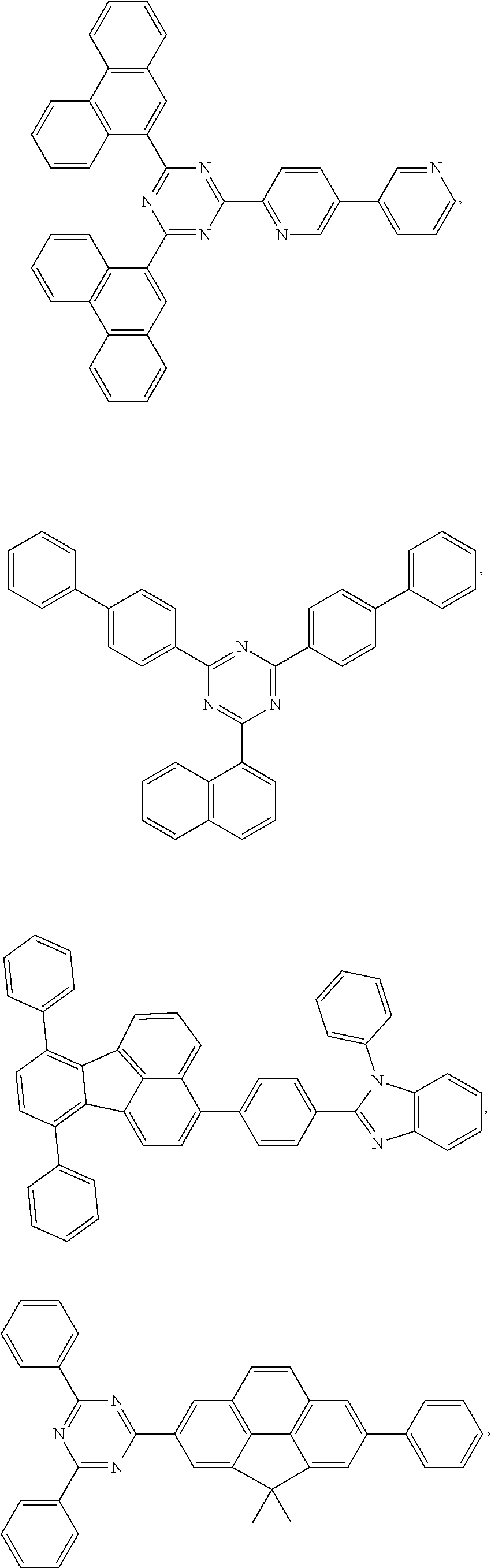
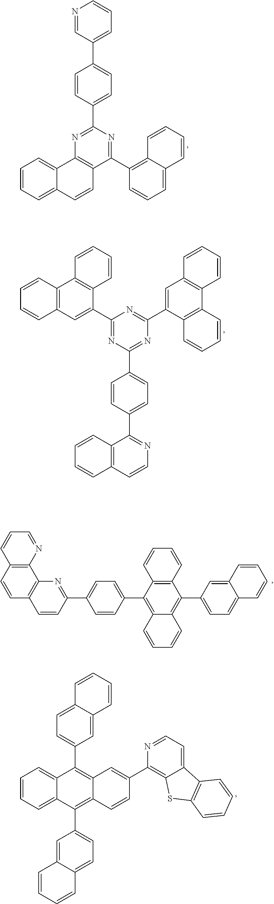

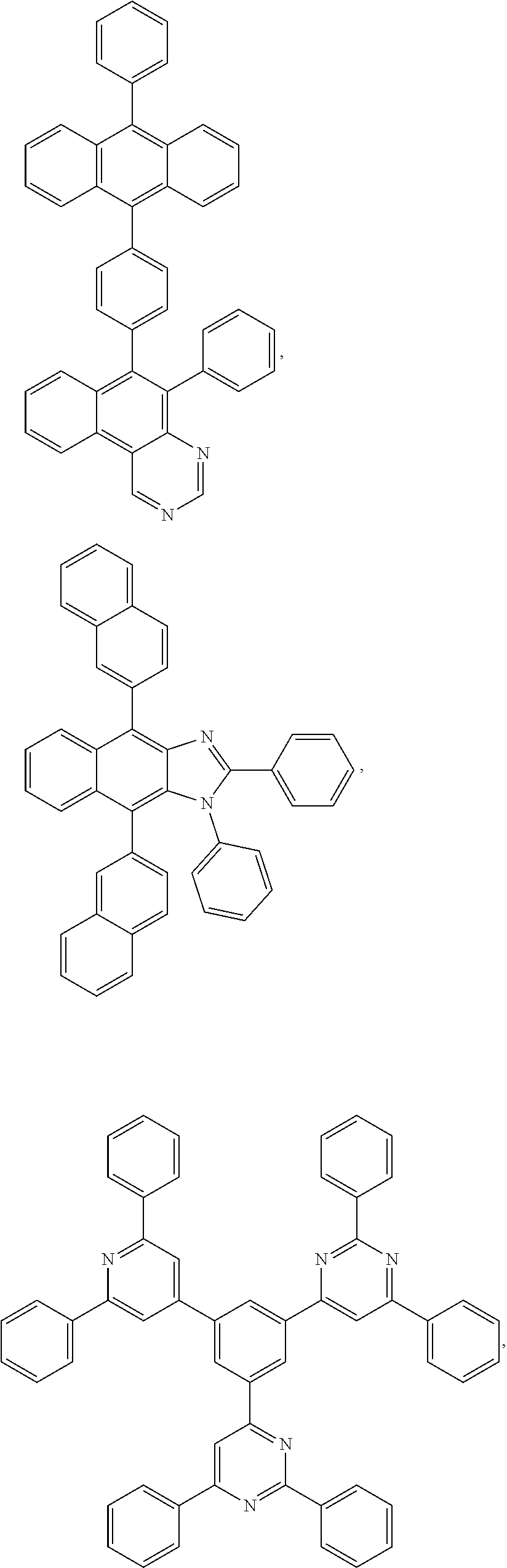

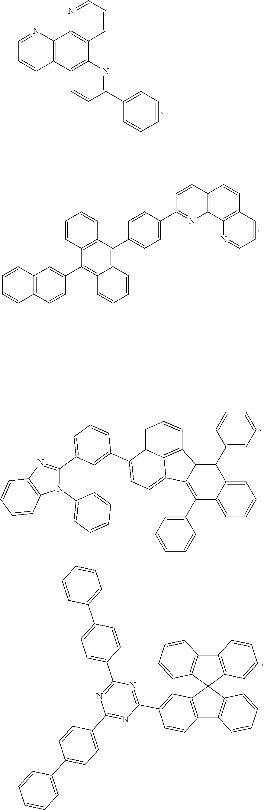


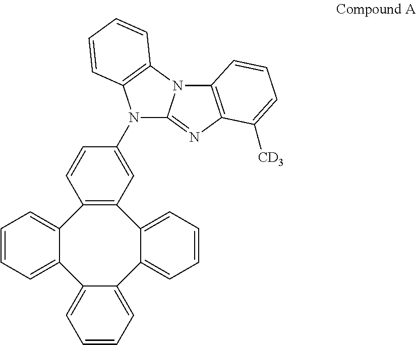

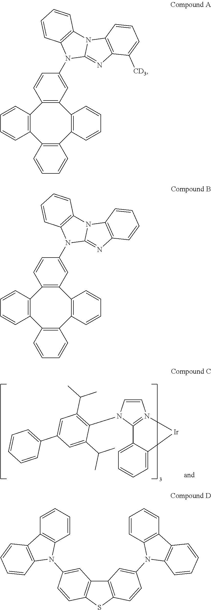
| TABLE 1 | |||||
| 1931 CIE | Emmax | Relative | Relative | ||
| Device | EML | x | y | [nm] | EQE@1000 nits | LT90@1000 nits |
| Example 1 | Compound A | 0.171 | 0.382 | 474 | 1.03 | 2.15 |
| Comparative | Compound B | 0.173 | 0.388 | 475 | 1.00 | 1.00 |
Claims (20)


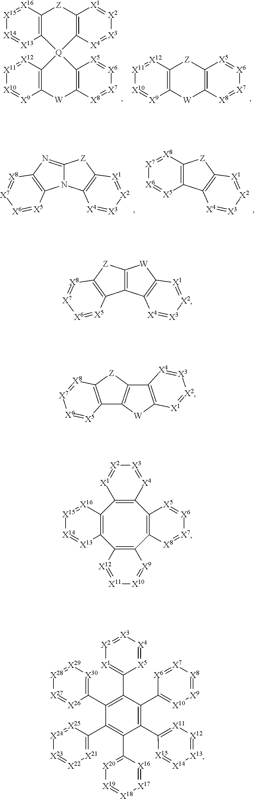
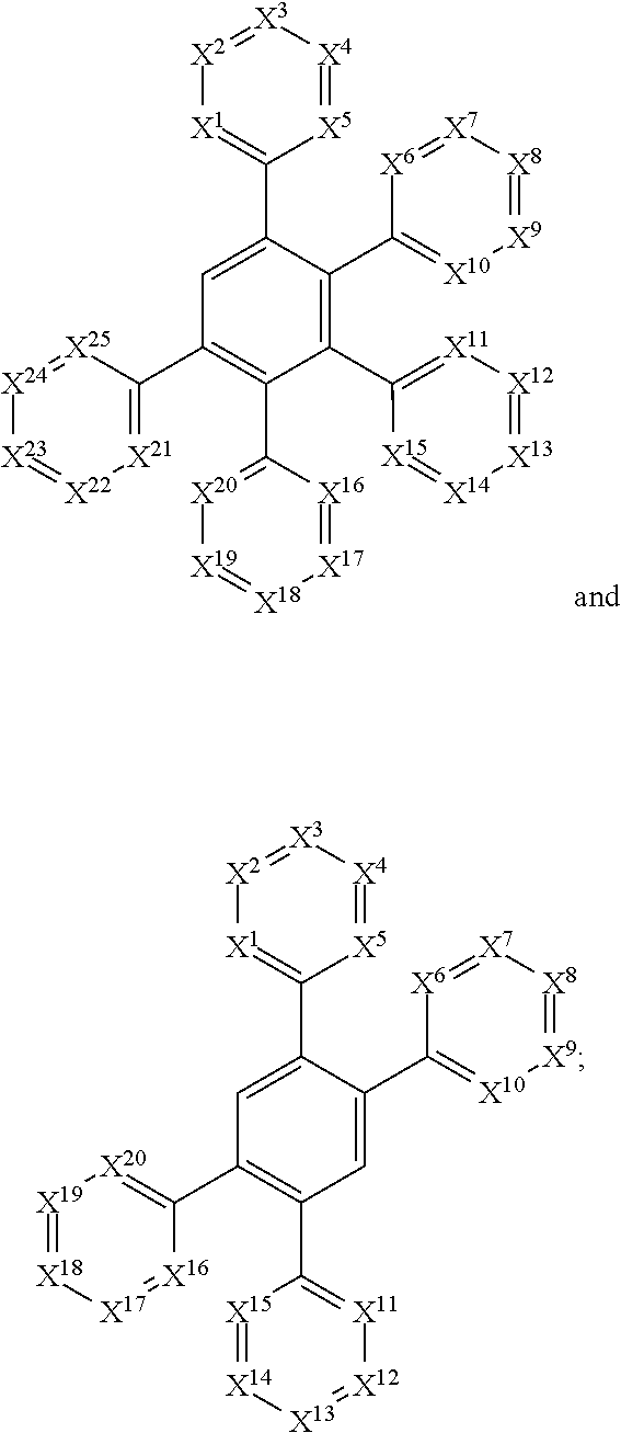
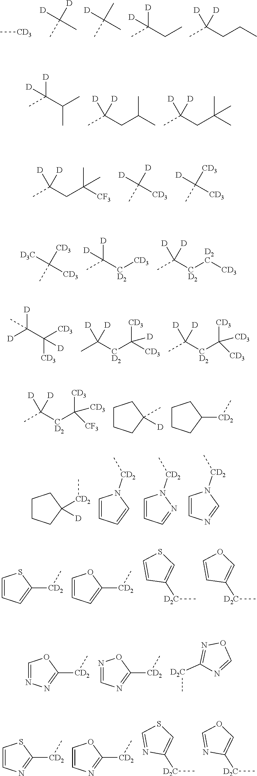

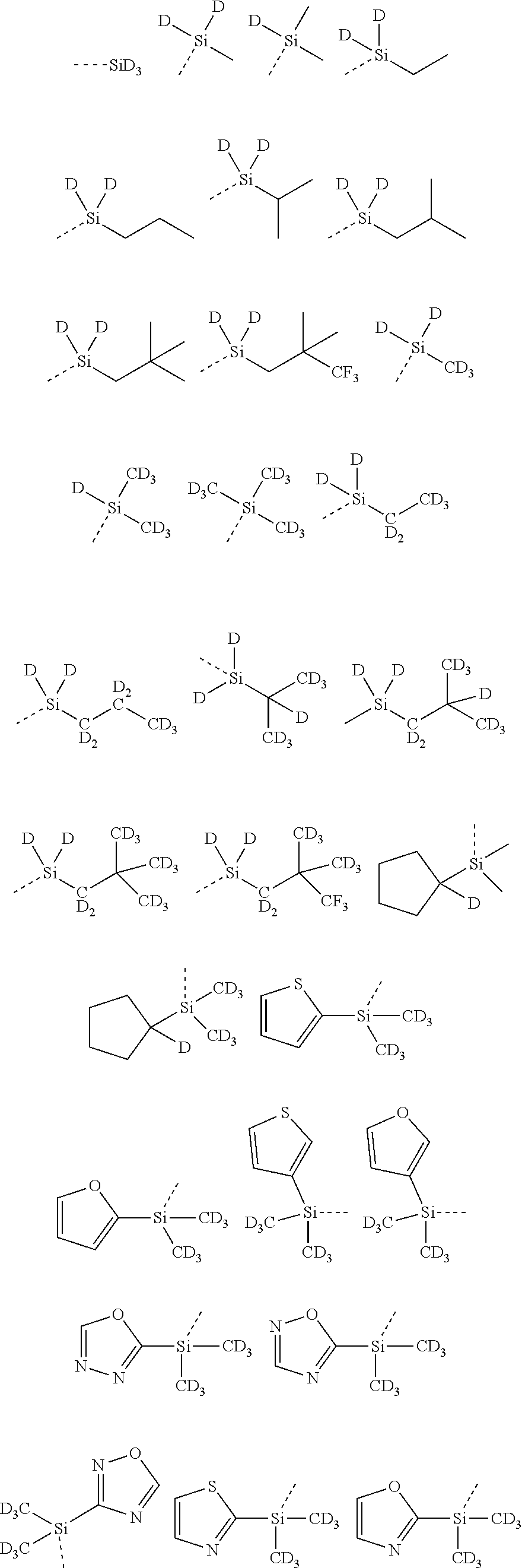


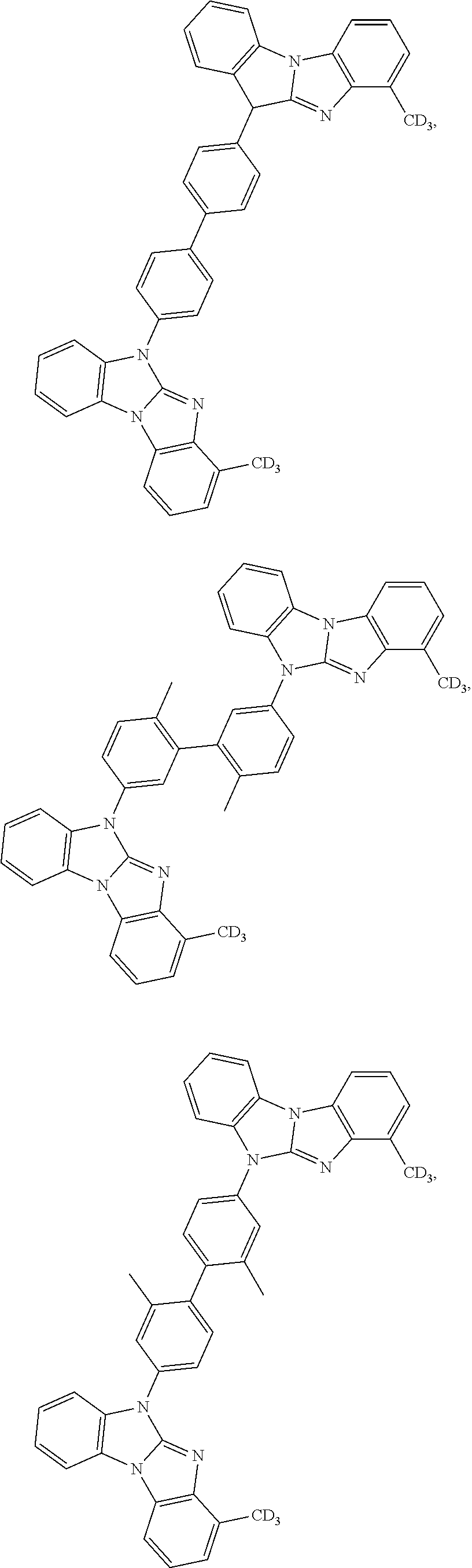
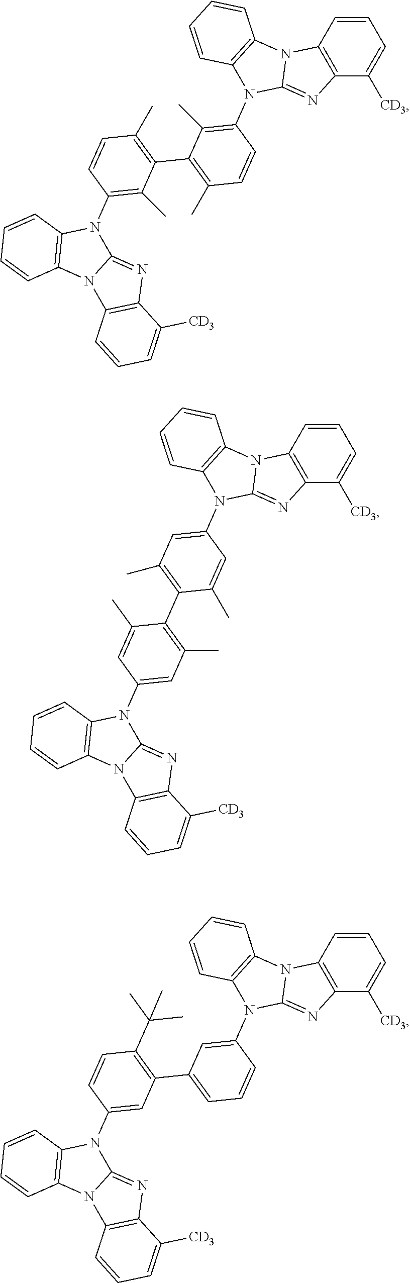

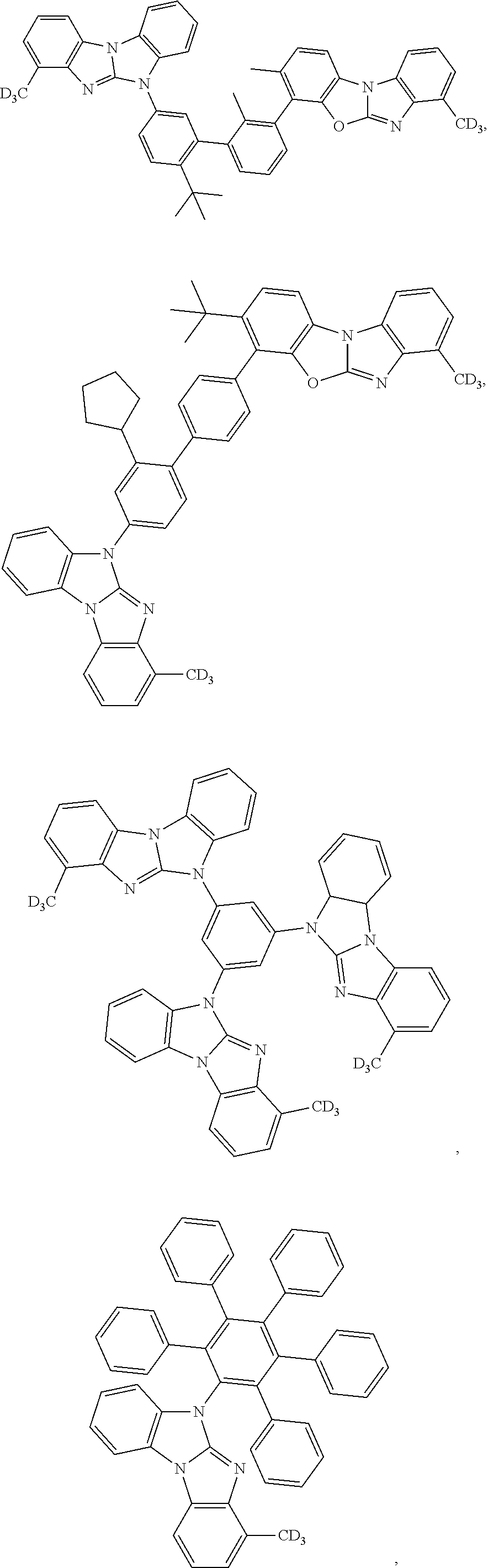


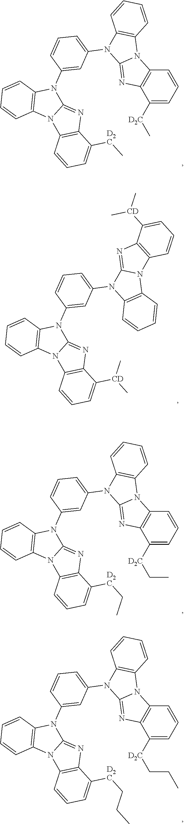


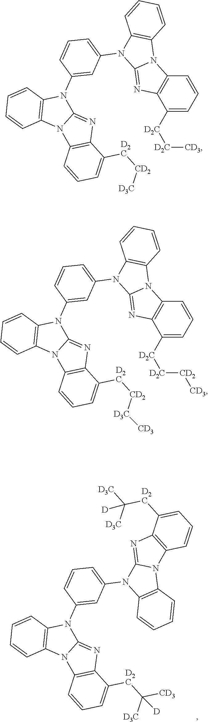
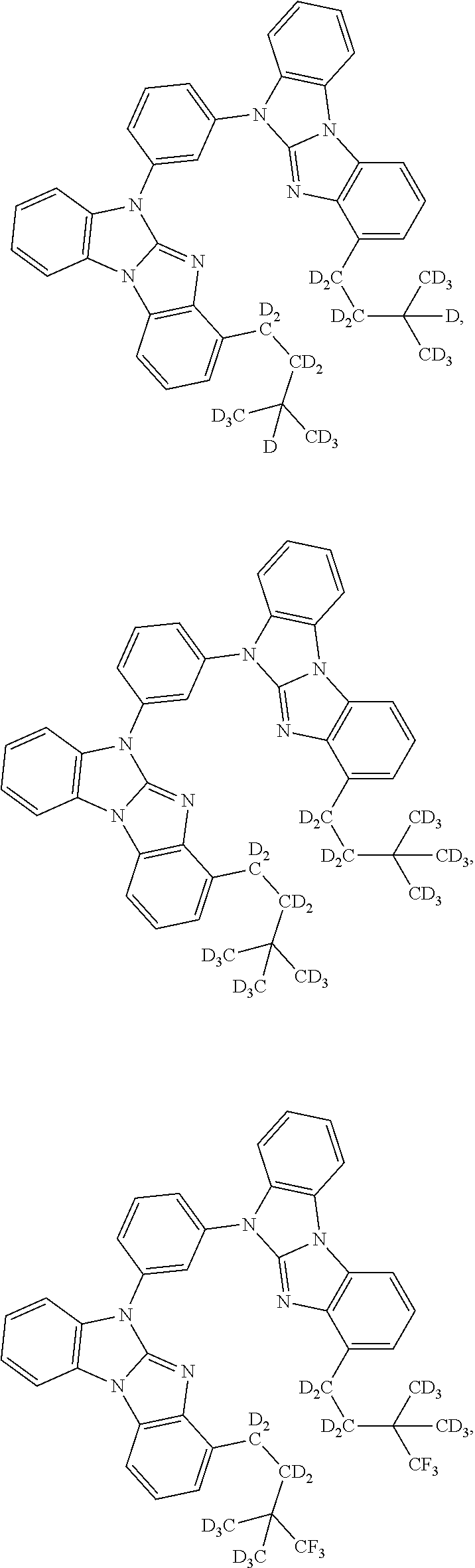
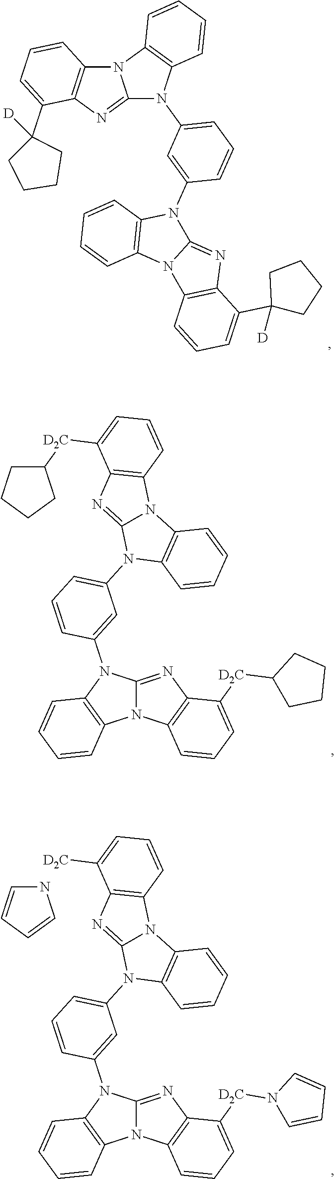
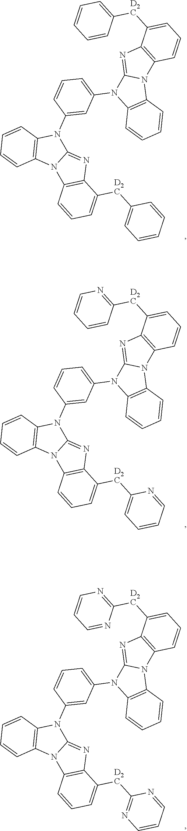
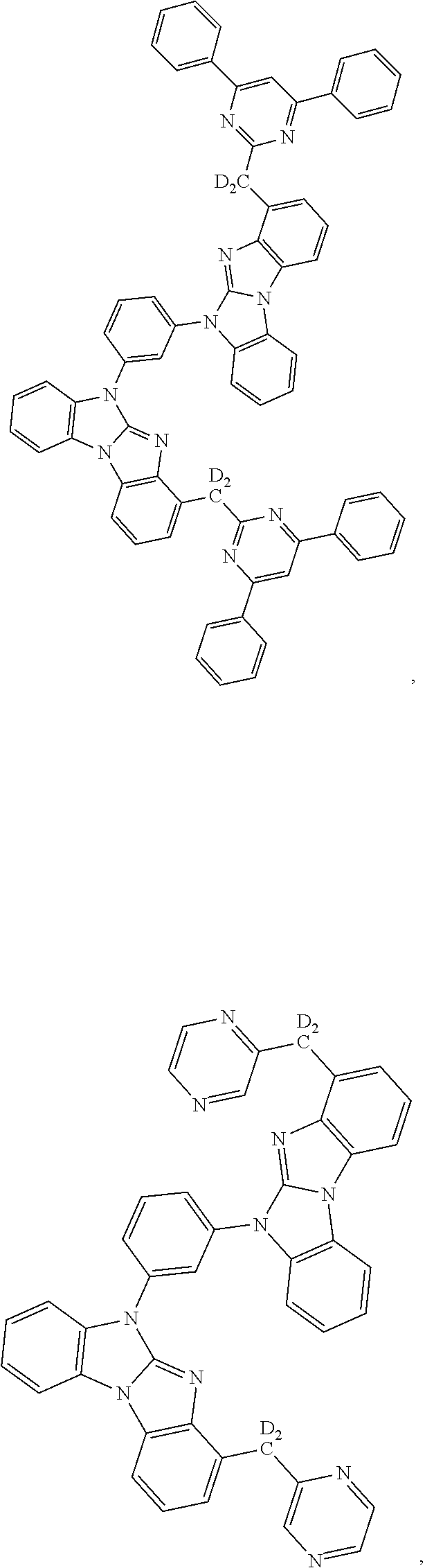


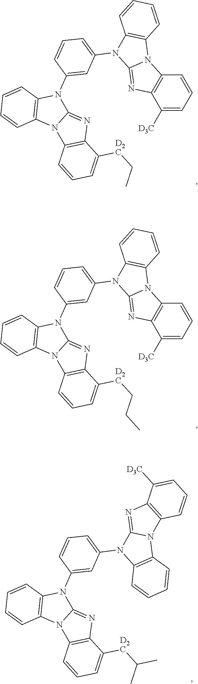
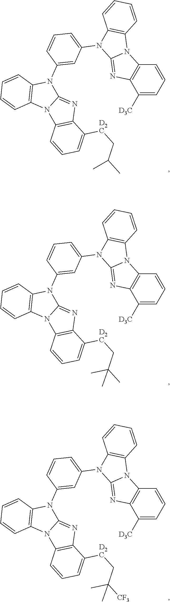
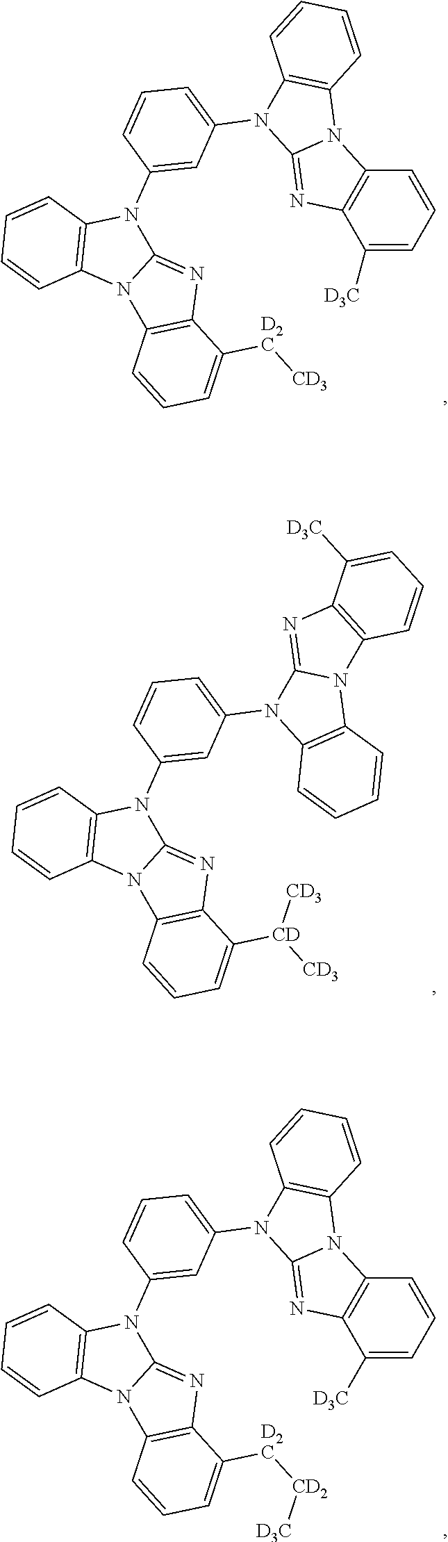

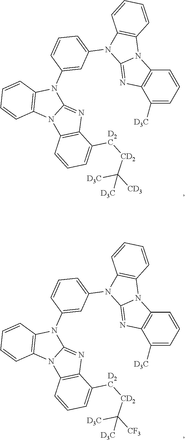

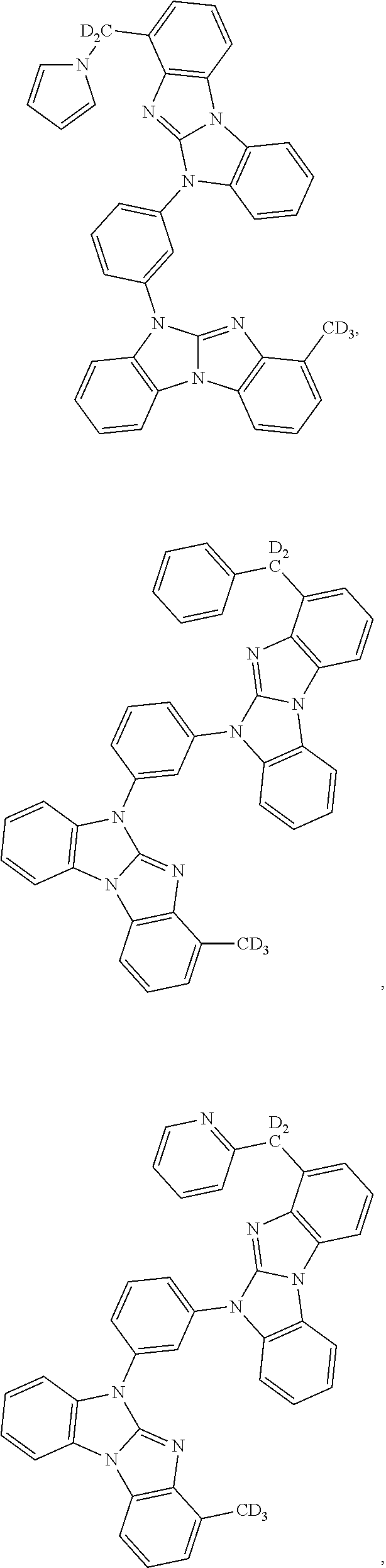

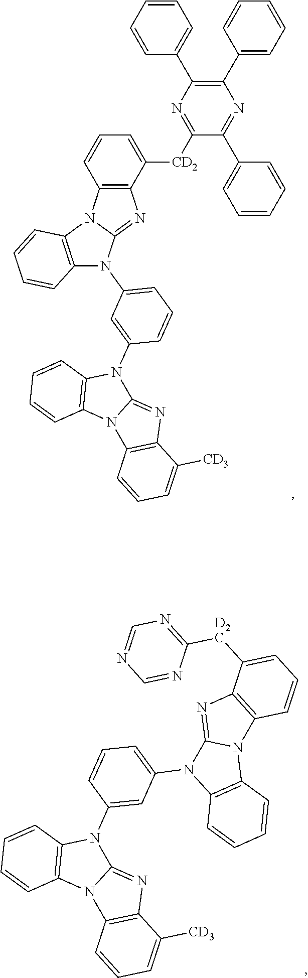


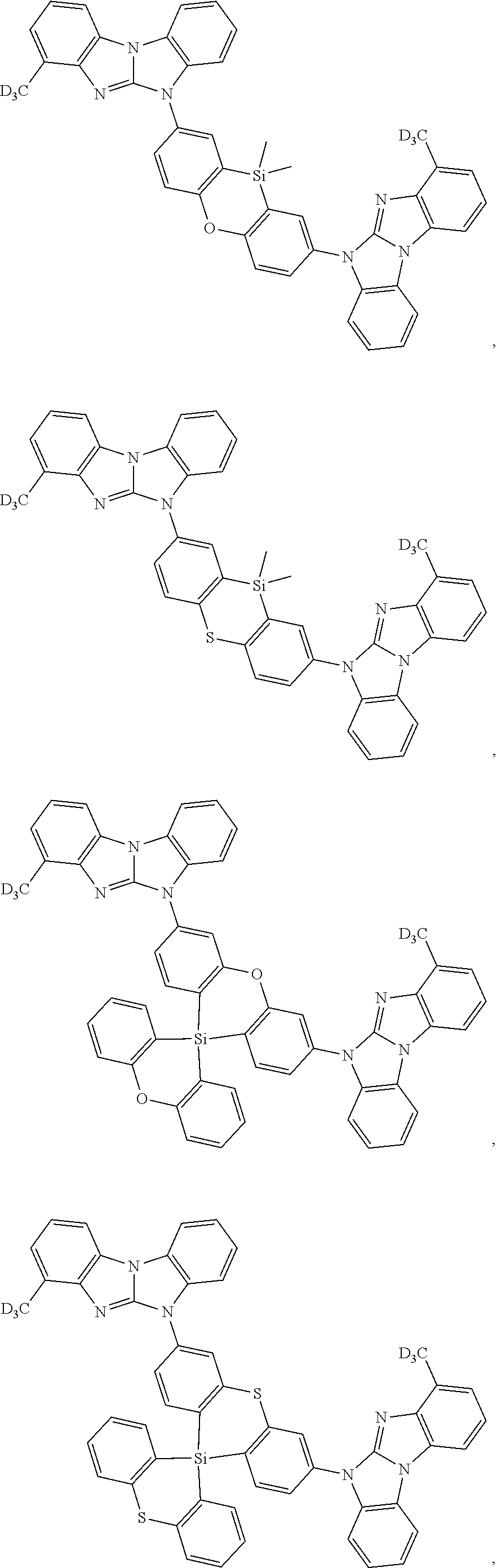


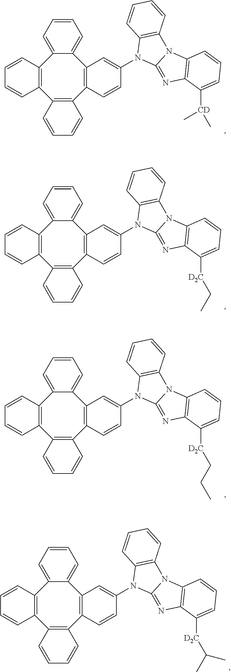


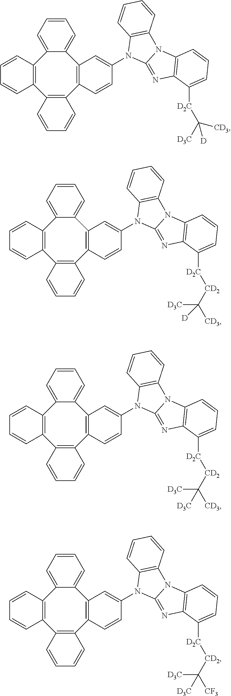


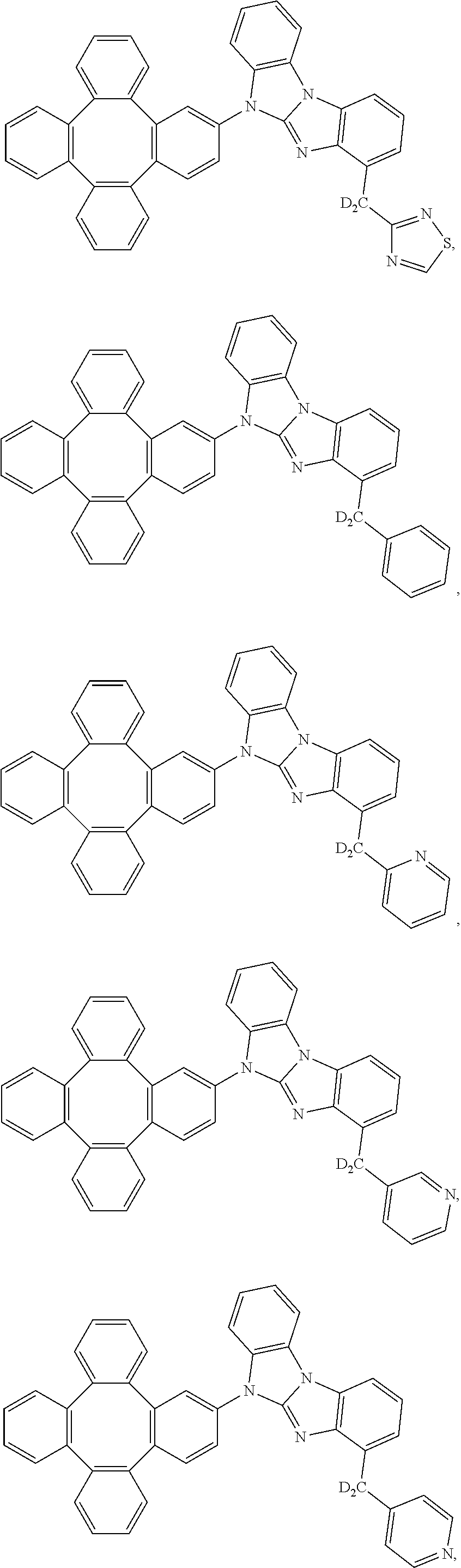
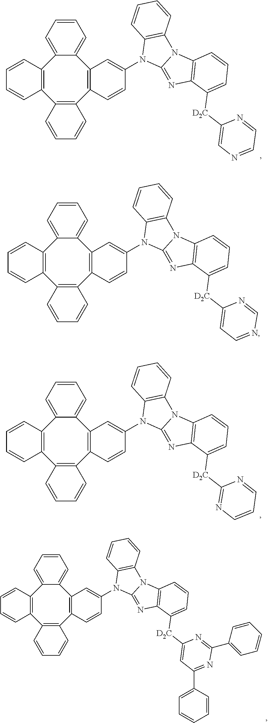

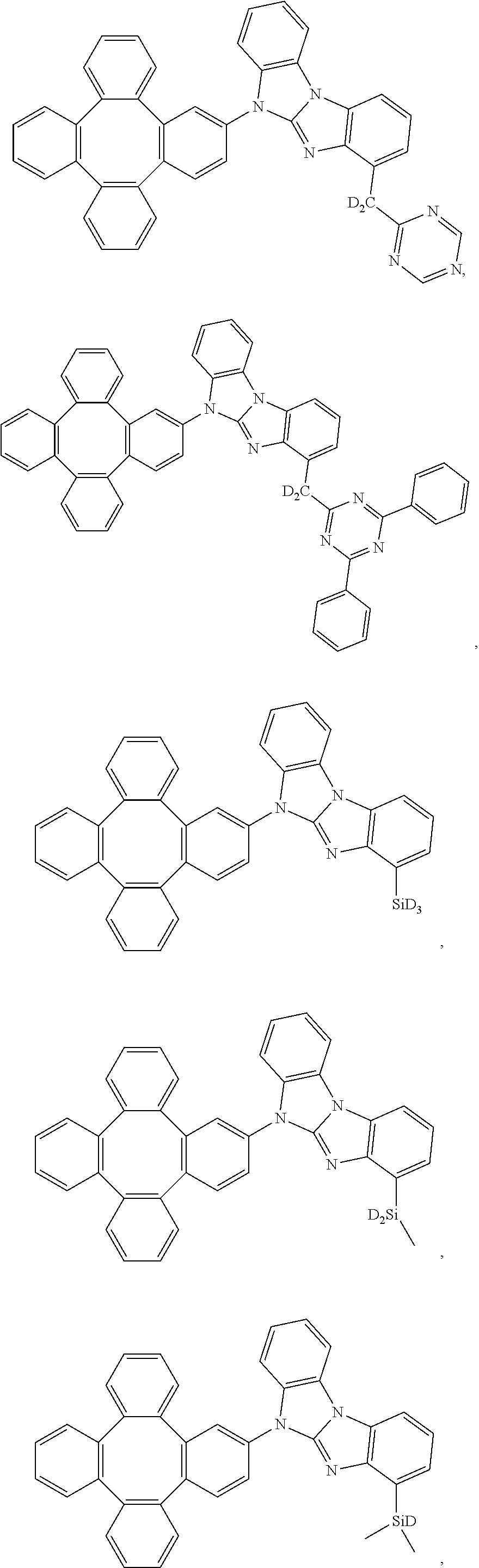

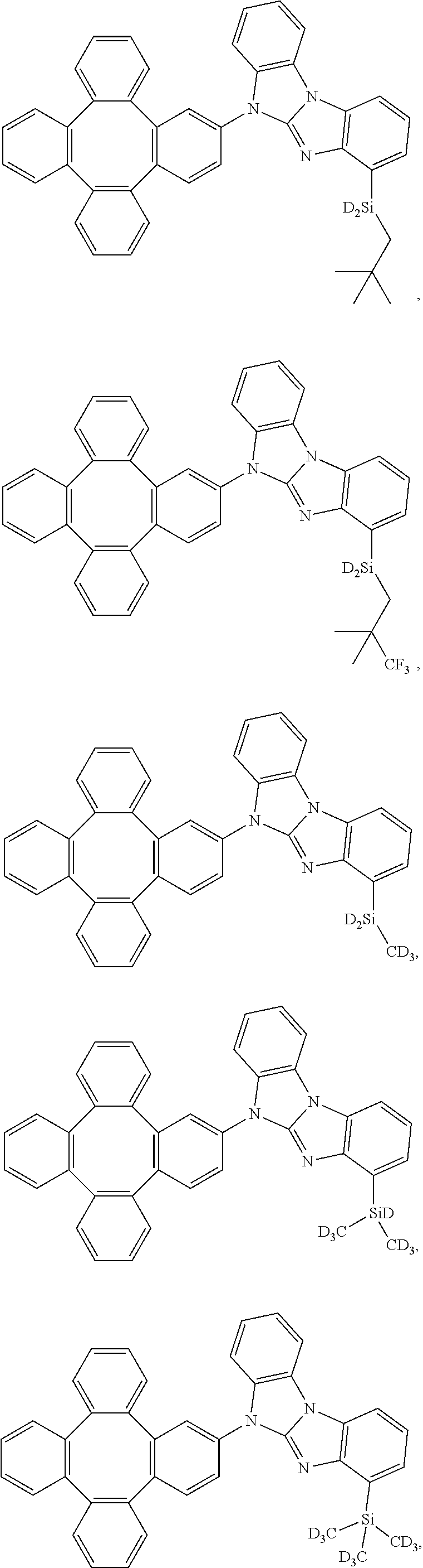
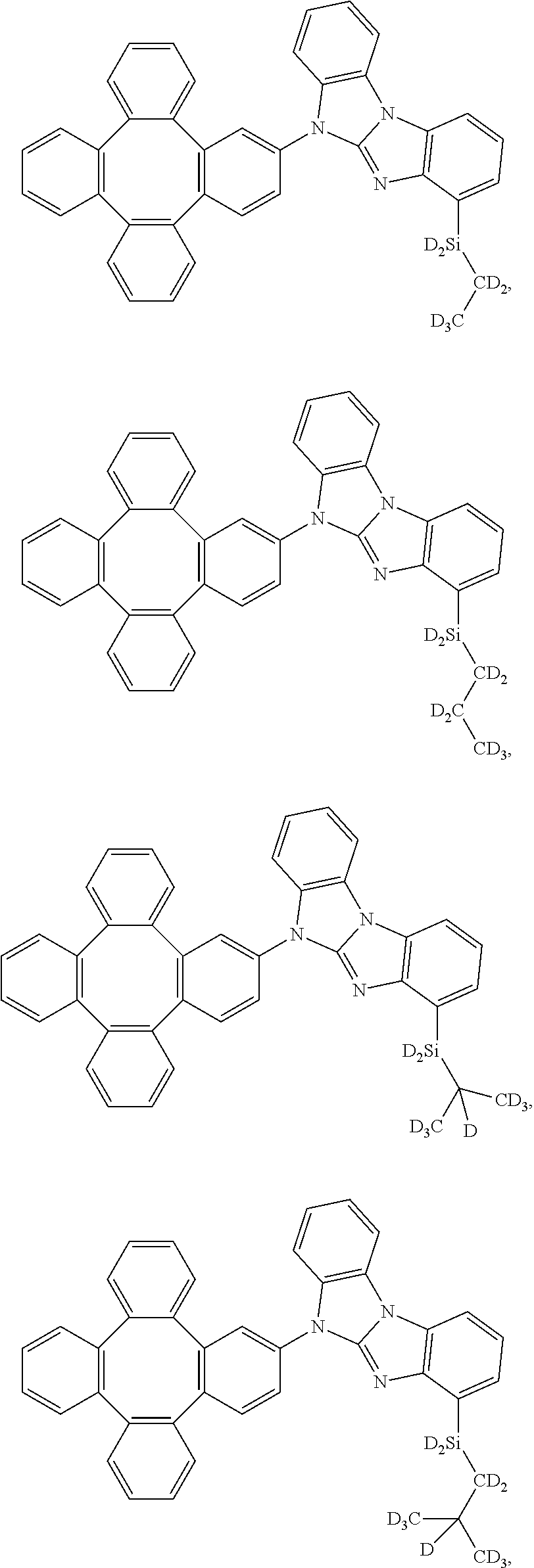
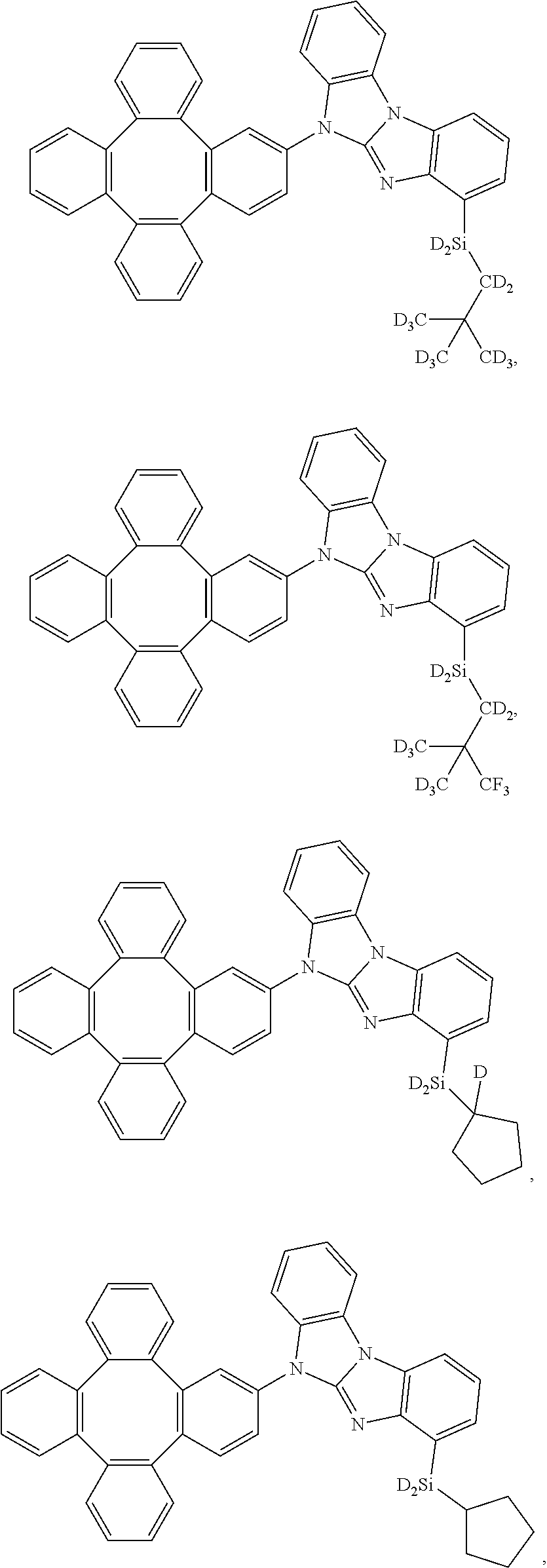


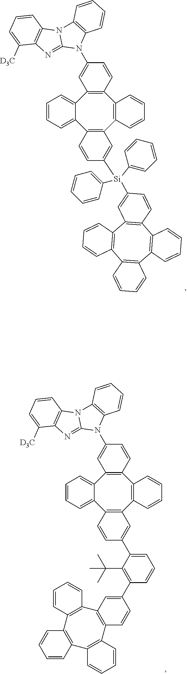

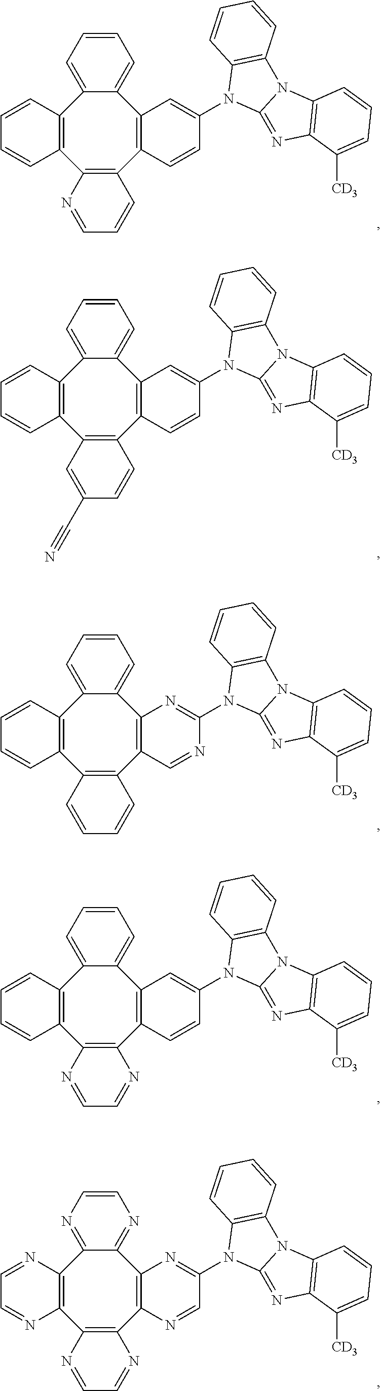

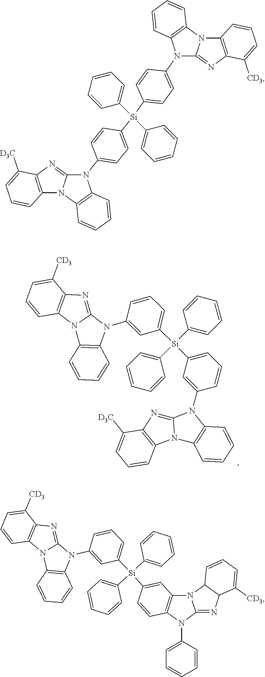

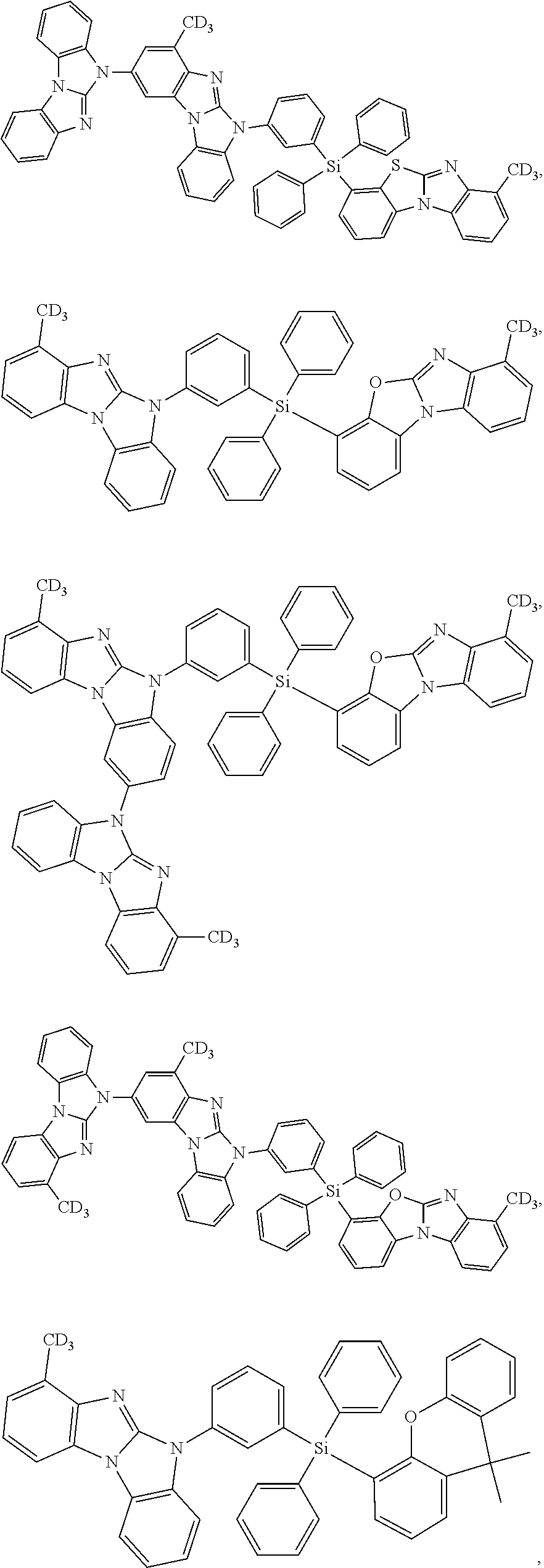


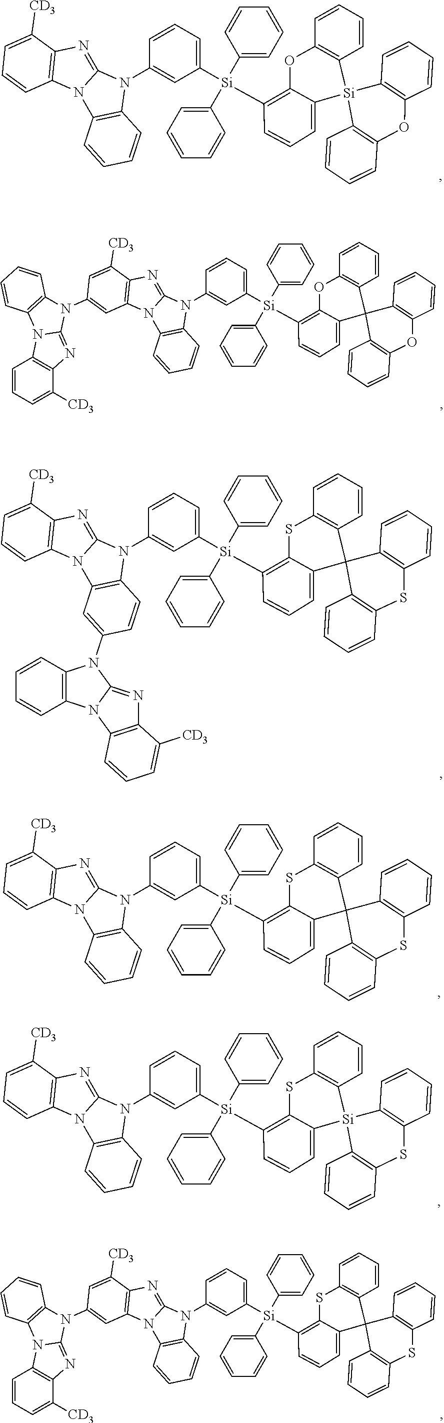

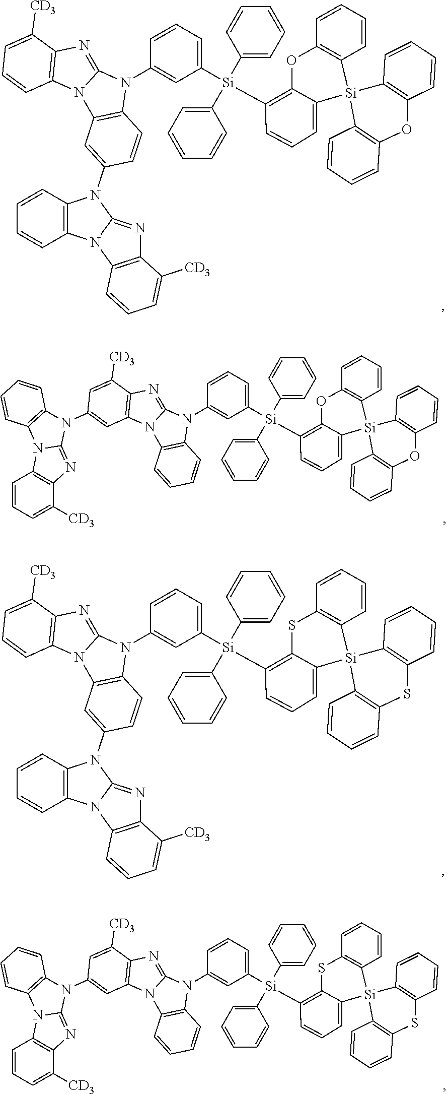

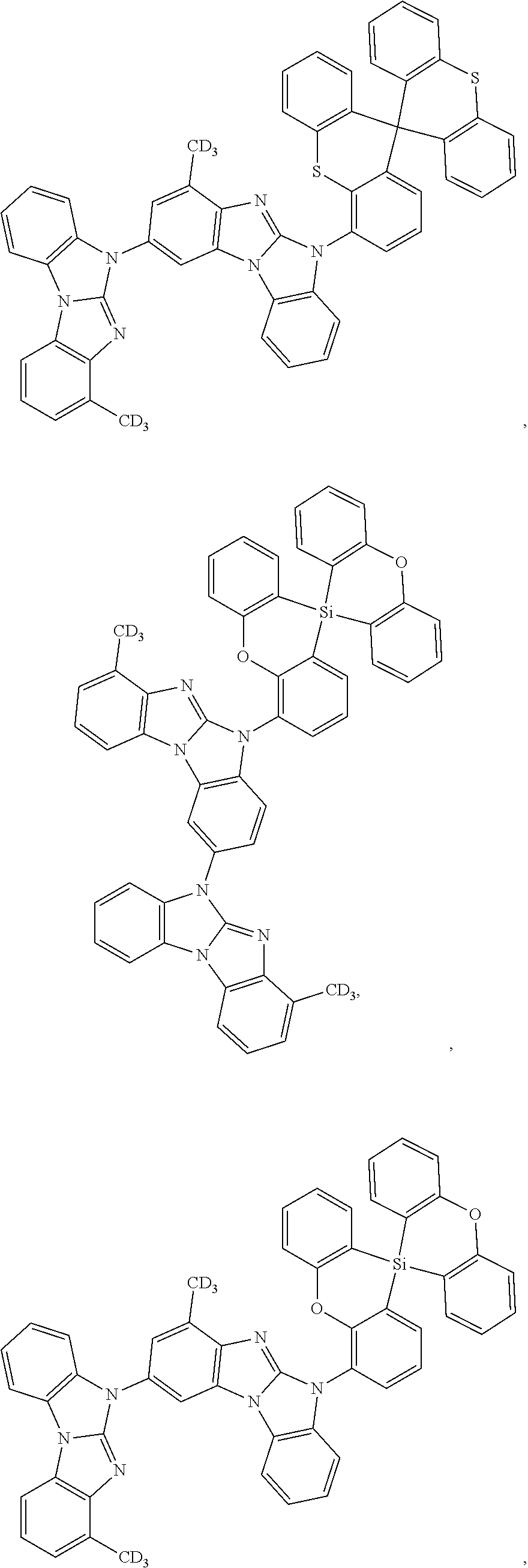

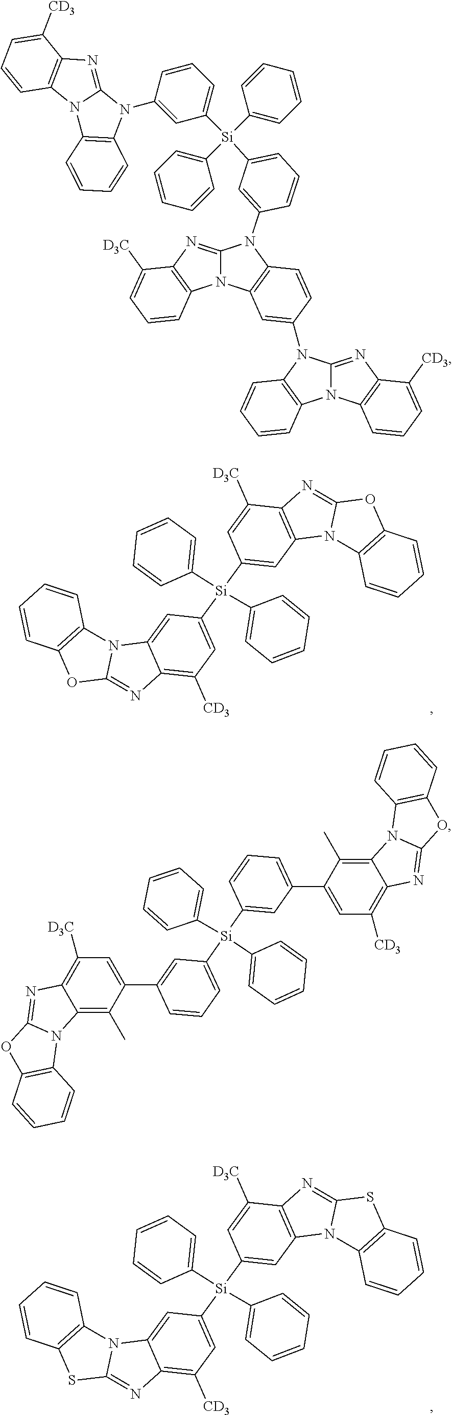
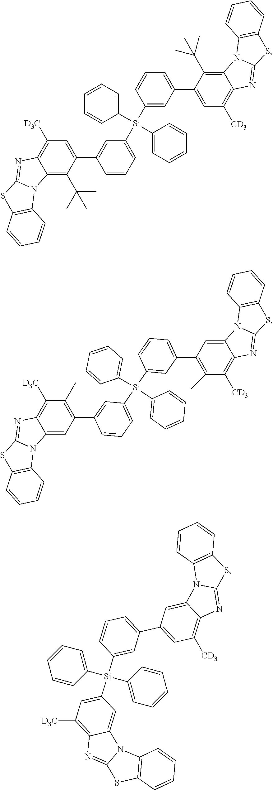


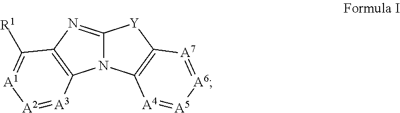


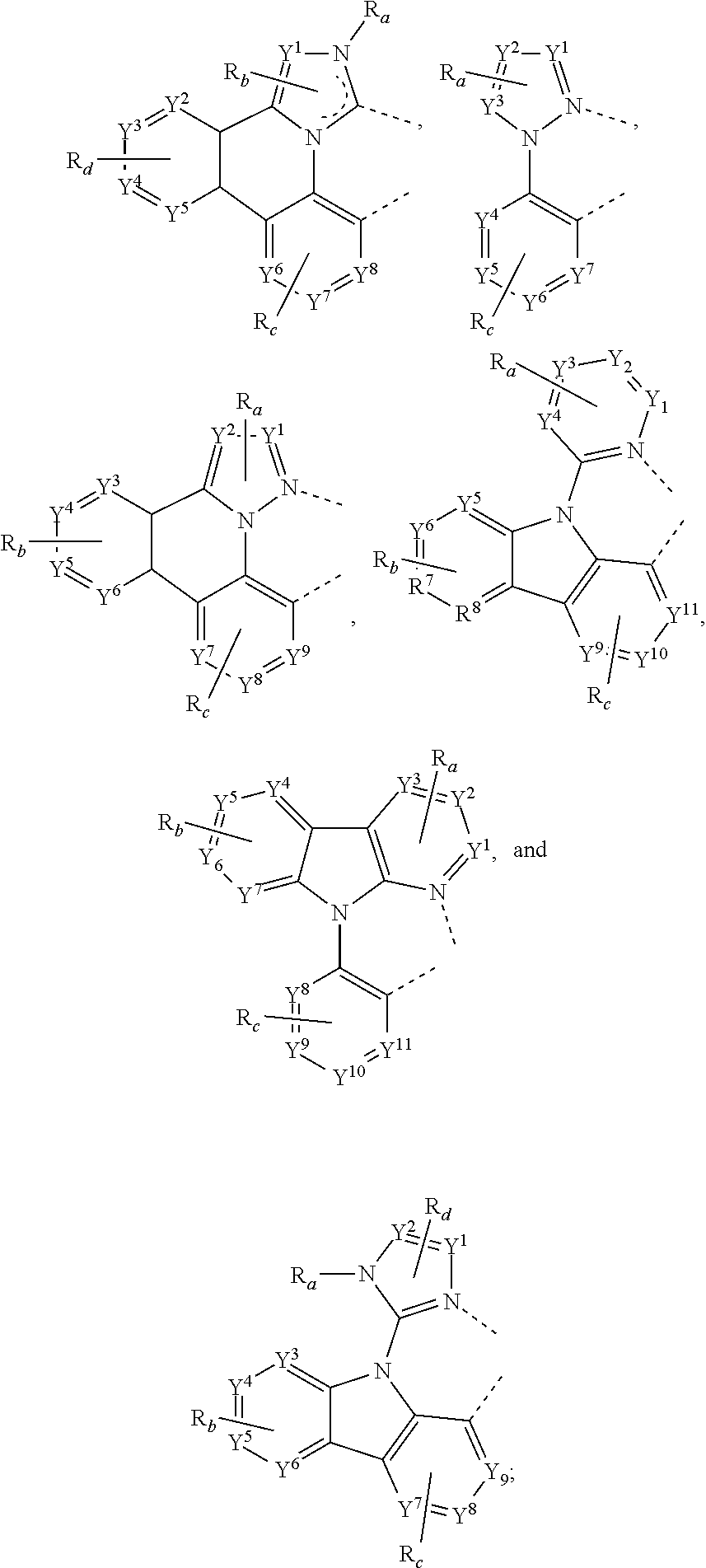


Priority Applications (2)
| Application Number | Priority Date | Filing Date | Title |
|---|---|---|---|
| US15/983,344 US11174259B2 (en) | 2017-06-23 | 2018-05-18 | Organic electroluminescent materials and devices |
| CN201810642213.2A CN109111448A (en) | 2017-06-23 | 2018-06-21 | Electroluminescent organic material and device |
Applications Claiming Priority (2)
| Application Number | Priority Date | Filing Date | Title |
|---|---|---|---|
| US201762524050P | 2017-06-23 | 2017-06-23 | |
| US15/983,344 US11174259B2 (en) | 2017-06-23 | 2018-05-18 | Organic electroluminescent materials and devices |
Publications (2)
| Publication Number | Publication Date |
|---|---|
| US20180370978A1 US20180370978A1 (en) | 2018-12-27 |
| US11174259B2 true US11174259B2 (en) | 2021-11-16 |
Family
ID=64691951
Family Applications (1)
| Application Number | Title | Priority Date | Filing Date |
|---|---|---|---|
| US15/983,344 Active 2039-08-19 US11174259B2 (en) | 2017-06-23 | 2018-05-18 | Organic electroluminescent materials and devices |
Country Status (2)
| Country | Link |
|---|---|
| US (1) | US11174259B2 (en) |
| CN (1) | CN109111448A (en) |
Cited By (2)
| Publication number | Priority date | Publication date | Assignee | Title |
|---|---|---|---|---|
| US20200017508A1 (en) * | 2018-07-13 | 2020-01-16 | Universal Display Corporation | Organic electroluminescent materials and devices |
| US11374181B2 (en) * | 2019-08-14 | 2022-06-28 | Universal Display Corporation | Organic electroluminescent materials and devices |
Families Citing this family (17)
| Publication number | Priority date | Publication date | Assignee | Title |
|---|---|---|---|---|
| US10636983B2 (en) | 2014-05-08 | 2020-04-28 | Universal Display Corporation | Organic electroluminescent materials and devices |
| US11084838B2 (en) | 2017-04-21 | 2021-08-10 | Universal Display Corporation | Organic electroluminescent materials and device |
| US10975113B2 (en) | 2017-04-21 | 2021-04-13 | Universal Display Corporation | Organic electroluminescent materials and devices |
| US11814403B2 (en) | 2017-06-23 | 2023-11-14 | Universal Display Corporation | Organic electroluminescent materials and devices |
| US11802136B2 (en) | 2017-06-23 | 2023-10-31 | Universal Display Corporation | Organic electroluminescent materials and devices |
| US11552261B2 (en) | 2017-06-23 | 2023-01-10 | Universal Display Corporation | Organic electroluminescent materials and devices |
| US11725022B2 (en) | 2017-06-23 | 2023-08-15 | Universal Display Corporation | Organic electroluminescent materials and devices |
| US11696492B2 (en) | 2017-09-07 | 2023-07-04 | Universal Display Corporation | Organic electroluminescent materials and devices |
| KR102694284B1 (en) * | 2018-10-11 | 2024-08-13 | 삼성디스플레이 주식회사 | Organic electroluminescence device and amine compound for organic electroluminescence device |
| US11476430B2 (en) | 2018-10-15 | 2022-10-18 | Universal Display Corporation | Organic electroluminescent materials and devices |
| JP2020158491A (en) * | 2019-03-26 | 2020-10-01 | ユニバーサル ディスプレイ コーポレイション | Organic electroluminescent materials and devices |
| KR102784317B1 (en) | 2019-07-30 | 2025-03-24 | 삼성디스플레이 주식회사 | Display device |
| US12295251B2 (en) | 2019-08-01 | 2025-05-06 | Universal Display Corporation | Organic electroluminescent materials and devices |
| CN110698494B (en) * | 2019-10-15 | 2021-08-31 | 浙江虹舞科技有限公司 | Charge transport material and organic light-emitting element |
| US11844275B2 (en) | 2019-10-18 | 2023-12-12 | Lg Display Co., Ltd. | Organic compound, organic light emitting diode and organic light emitting deice including the organic compound |
| US12486288B2 (en) | 2020-10-12 | 2025-12-02 | University Of Southern California | Fast phosphors utilizing HP2H ligands |
| CN115403608B (en) * | 2022-09-26 | 2025-05-02 | 上海天马微电子有限公司 | A spirofluorene silicon compound and its electroluminescent application |
Citations (142)
| Publication number | Priority date | Publication date | Assignee | Title |
|---|---|---|---|---|
| US4769292A (en) | 1987-03-02 | 1988-09-06 | Eastman Kodak Company | Electroluminescent device with modified thin film luminescent zone |
| US5061569A (en) | 1990-07-26 | 1991-10-29 | Eastman Kodak Company | Electroluminescent device with organic electroluminescent medium |
| US5247190A (en) | 1989-04-20 | 1993-09-21 | Cambridge Research And Innovation Limited | Electroluminescent devices |
| EP0650955A1 (en) | 1993-11-01 | 1995-05-03 | Hodogaya Chemical Co., Ltd. | Amine compound and electro-luminescence device comprising same |
| US5703436A (en) | 1994-12-13 | 1997-12-30 | The Trustees Of Princeton University | Transparent contacts for organic devices |
| US5707745A (en) | 1994-12-13 | 1998-01-13 | The Trustees Of Princeton University | Multicolor organic light emitting devices |
| US5834893A (en) | 1996-12-23 | 1998-11-10 | The Trustees Of Princeton University | High efficiency organic light emitting devices with light directing structures |
| US5844363A (en) | 1997-01-23 | 1998-12-01 | The Trustees Of Princeton Univ. | Vacuum deposited, non-polymeric flexible organic light emitting devices |
| US6013982A (en) | 1996-12-23 | 2000-01-11 | The Trustees Of Princeton University | Multicolor display devices |
| US6087196A (en) | 1998-01-30 | 2000-07-11 | The Trustees Of Princeton University | Fabrication of organic semiconductor devices using ink jet printing |
| US6091195A (en) | 1997-02-03 | 2000-07-18 | The Trustees Of Princeton University | Displays having mesa pixel configuration |
| US6097147A (en) | 1998-09-14 | 2000-08-01 | The Trustees Of Princeton University | Structure for high efficiency electroluminescent device |
| WO2001039234A2 (en) | 1999-11-24 | 2001-05-31 | The Trustees Of Princeton University | Organic light emitting diode having a blue phosphorescent molecule as an emitter |
| US6294398B1 (en) | 1999-11-23 | 2001-09-25 | The Trustees Of Princeton University | Method for patterning devices |
| US6303238B1 (en) | 1997-12-01 | 2001-10-16 | The Trustees Of Princeton University | OLEDs doped with phosphorescent compounds |
| US6337102B1 (en) | 1997-11-17 | 2002-01-08 | The Trustees Of Princeton University | Low pressure vapor phase deposition of organic thin films |
| WO2002002714A2 (en) | 2000-06-30 | 2002-01-10 | E.I. Du Pont De Nemours And Company | Electroluminescent iridium compounds with fluorinated phenylpyridines, phenylpyrimidines, and phenylquinolines and devices made with such compounds |
| WO2002015645A1 (en) | 2000-08-11 | 2002-02-21 | The Trustees Of Princeton University | Organometallic compounds and emission-shifting organic electrophosphorescence |
| US20020034656A1 (en) | 1998-09-14 | 2002-03-21 | Thompson Mark E. | Organometallic complexes as phosphorescent emitters in organic LEDs |
| EP1238981A2 (en) | 2001-03-08 | 2002-09-11 | Canon Kabushiki Kaisha | Metal coordination compound, luminescence device and display apparatus |
| US20020134984A1 (en) | 2001-02-01 | 2002-09-26 | Fuji Photo Film Co., Ltd. | Transition metal complex and light-emitting device |
| US20020158242A1 (en) | 1999-12-31 | 2002-10-31 | Se-Hwan Son | Electronic device comprising organic compound having p-type semiconducting characteristics |
| US6528187B1 (en) | 1998-09-08 | 2003-03-04 | Fuji Photo Film Co., Ltd. | Material for luminescence element and luminescence element using the same |
| WO2003040257A1 (en) | 2001-11-07 | 2003-05-15 | E. I. Du Pont De Nemours And Company | Electroluminescent platinum compounds and devices made with such compounds |
| WO2003060956A2 (en) | 2002-01-18 | 2003-07-24 | Lg Chem, Ltd. | New material for transporting electrons and organic electroluminescent display using the same |
| US20030138657A1 (en) | 2000-12-07 | 2003-07-24 | Canon Kabushiki Kaisha | Deuterated semi-conducting organic compounds used for opto-electronic devices |
| US20030152802A1 (en) | 2001-06-19 | 2003-08-14 | Akira Tsuboyama | Metal coordination compound and organic liminescence device |
| US20030162053A1 (en) | 1996-06-25 | 2003-08-28 | Marks Tobin J. | Organic light - emitting diodes and methods for assembly and enhanced charge injection |
| US20030175553A1 (en) | 2001-12-28 | 2003-09-18 | Thompson Mark E. | White light emitting oleds from combined monomer and aggregate emission |
| US20030230980A1 (en) | 2002-06-18 | 2003-12-18 | Forrest Stephen R | Very low voltage, high efficiency phosphorescent oled in a p-i-n structure |
| US6687266B1 (en) | 2002-11-08 | 2004-02-03 | Universal Display Corporation | Organic light emitting materials and devices |
| US20040036077A1 (en) | 2002-08-22 | 2004-02-26 | Fuji Photo Film Co., Ltd. | Light emitting element |
| US20040137267A1 (en) | 2002-12-27 | 2004-07-15 | Fuji Photo Film Co., Ltd. | Organic electroluminescent device |
| US20040137268A1 (en) | 2002-12-27 | 2004-07-15 | Fuji Photo Film Co., Ltd. | Organic electroluminescent device |
| US20040174116A1 (en) | 2001-08-20 | 2004-09-09 | Lu Min-Hao Michael | Transparent electrodes |
| WO2004093207A2 (en) | 2003-04-15 | 2004-10-28 | Covion Organic Semiconductors Gmbh | Mixtures of matrix materials and organic semiconductors capable of emission, use of the same and electronic components containing said mixtures |
| WO2004107822A1 (en) | 2003-05-29 | 2004-12-09 | Nippon Steel Chemical Co., Ltd. | Organic electroluminescent element |
| WO2004111066A1 (en) | 2003-06-09 | 2004-12-23 | Hitachi Chemical Co., Ltd. | Metal coordination compound, polymer composition, and organic electroluminescence element using them |
| US6835469B2 (en) | 2001-10-17 | 2004-12-28 | The University Of Southern California | Phosphorescent compounds and devices comprising the same |
| JP2005011610A (en) | 2003-06-18 | 2005-01-13 | Nippon Steel Chem Co Ltd | Organic electroluminescence device |
| US20050025993A1 (en) | 2003-07-25 | 2005-02-03 | Thompson Mark E. | Materials and structures for enhancing the performance of organic light emitting devices |
| WO2005014551A1 (en) | 2003-08-07 | 2005-02-17 | Nippon Steel Chemical Co., Ltd. | Aluminum chelate compelx for organic el material |
| WO2005019373A2 (en) | 2003-08-19 | 2005-03-03 | Basf Aktiengesellschaft | Transition metal complexes comprising carbene ligands serving as emitters for organic light-emitting diodes (oled's) |
| WO2005030900A1 (en) | 2003-09-25 | 2005-04-07 | Nippon Steel Chemical Co., Ltd. | Organic electroluminescent device |
| US20050112407A1 (en) | 2003-11-21 | 2005-05-26 | Fuji Photo Film Co., Ltd. | Organic electroluminescent device |
| WO2005089025A1 (en) | 2004-03-15 | 2005-09-22 | Nippon Steel Chemical Co., Ltd. | Organic electroluminescent device |
| US20050238919A1 (en) | 2004-04-23 | 2005-10-27 | Fuji Photo Film Co., Ltd. | Organic electroluminescent device |
| US20050244673A1 (en) | 2002-08-27 | 2005-11-03 | Fujitsu Limited | Organometallic complex, organic EL element and organic EL display |
| US20050260449A1 (en) | 2004-05-18 | 2005-11-24 | Robert Walters | Complexes with tridentate ligands |
| US20050260441A1 (en) | 2004-05-18 | 2005-11-24 | Thompson Mark E | Luminescent compounds with carbene ligands |
| WO2005123873A1 (en) | 2004-06-17 | 2005-12-29 | Konica Minolta Holdings, Inc. | Organic electroluminescent device material, organic electroluminescent device, display and illuminating device |
| US20060008670A1 (en) | 2004-07-06 | 2006-01-12 | Chun Lin | Organic light emitting materials and devices |
| WO2006009024A1 (en) | 2004-07-23 | 2006-01-26 | Konica Minolta Holdings, Inc. | Organic electroluminescent device, display and illuminating device |
| WO2006056418A2 (en) | 2004-11-25 | 2006-06-01 | Basf Aktiengesellschaft | Use of transition metal carbene complexes in organic light-emitting diodes (oleds) |
| WO2006072002A2 (en) | 2004-12-30 | 2006-07-06 | E.I. Dupont De Nemours And Company | Organometallic complexes |
| US7087321B2 (en) | 2003-04-22 | 2006-08-08 | Universal Display Corporation | Organic light emitting devices having reduced pixel shrinkage |
| WO2006082742A1 (en) | 2005-02-04 | 2006-08-10 | Konica Minolta Holdings, Inc. | Organic electroluminescent device material, organic electroluminescent device, display and illuminating device |
| US7090928B2 (en) | 2003-04-01 | 2006-08-15 | The University Of Southern California | Binuclear compounds |
| US20060202194A1 (en) | 2005-03-08 | 2006-09-14 | Jeong Hyun C | Red phosphorescene compounds and organic electroluminescence device using the same |
| WO2006098120A1 (en) | 2005-03-16 | 2006-09-21 | Konica Minolta Holdings, Inc. | Organic electroluminescent device material and organic electroluminescent device |
| WO2006100298A1 (en) | 2005-03-24 | 2006-09-28 | Basf Aktiengesellschaft | Use of compounds containing aromatic or heteroaromatic rings linked via carbonyl group-containing groups, for use as matrix materials in organic light-emitting diodes |
| WO2006103874A1 (en) | 2005-03-29 | 2006-10-05 | Konica Minolta Holdings, Inc. | Organic electroluminescent device material, organic electroluminescent device, display and illuminating device |
| US20060240279A1 (en) | 2005-04-21 | 2006-10-26 | Vadim Adamovich | Non-blocked phosphorescent OLEDs |
| WO2006114966A1 (en) | 2005-04-18 | 2006-11-02 | Konica Minolta Holdings, Inc. | Organic electroluminescent device, display and illuminating device |
| US20060251923A1 (en) | 2005-05-06 | 2006-11-09 | Chun Lin | Stability OLED materials and devices |
| EP1725079A1 (en) | 2004-03-11 | 2006-11-22 | Mitsubishi Chemical Corporation | Composition for charge-transporting film and ion compound, charge-transporting film and organic electroluminescent device using same, and method for manufacturing organic electroluminescent device and method for producing charge-transporting film |
| US20060263635A1 (en) | 2005-05-06 | 2006-11-23 | Fuji Photo Film Co., Ltd. | Organic electroluminescent device |
| US20060280965A1 (en) | 2005-05-31 | 2006-12-14 | Raymond Kwong | Triphenylene hosts in phosphorescent light emitting diodes |
| WO2006132173A1 (en) | 2005-06-07 | 2006-12-14 | Nippon Steel Chemical Co., Ltd. | Organic metal complex and organic electroluminescent device using same |
| US7154114B2 (en) | 2004-05-18 | 2006-12-26 | Universal Display Corporation | Cyclometallated iridium carbene complexes for use as hosts |
| WO2007002683A2 (en) | 2005-06-27 | 2007-01-04 | E. I. Du Pont De Nemours And Company | Electrically conductive polymer compositions |
| WO2007004380A1 (en) | 2005-07-01 | 2007-01-11 | Konica Minolta Holdings, Inc. | Organic electroluminescent element material, organic electroluminescent element, display device, and lighting equipment |
| JP2007123392A (en) | 2005-10-26 | 2007-05-17 | Konica Minolta Holdings Inc | Organic electroluminescence element, display device and lighting device |
| WO2007063796A1 (en) | 2005-12-01 | 2007-06-07 | Nippon Steel Chemical Co., Ltd. | Organic electroluminescent device |
| WO2007063754A1 (en) | 2005-12-01 | 2007-06-07 | Nippon Steel Chemical Co., Ltd. | Compound for organic electroluminescent element and organic electroluminescent element |
| US7250226B2 (en) | 2001-08-31 | 2007-07-31 | Nippon Hoso Kyokai | Phosphorescent compound, a phosphorescent composition and an organic light-emitting device |
| US20070190359A1 (en) | 2006-02-10 | 2007-08-16 | Knowles David B | Metal complexes of cyclometallated imidazo[1,2-ƒ]phenanthridine and diimidazo[1,2-a:1',2'-c]quinazoline ligands and isoelectronic and benzannulated analogs thereof |
| JP2007254297A (en) | 2006-03-20 | 2007-10-04 | Nippon Steel Chem Co Ltd | Luminescent layer compound and organic electroluminescent device |
| US20070278938A1 (en) | 2006-04-26 | 2007-12-06 | Idemitsu Kosan Co., Ltd. | Aromatic amine derivative and electroluminescence device using the same |
| US20080015355A1 (en) | 2004-06-28 | 2008-01-17 | Thomas Schafer | Electroluminescent Metal Complexes With Triazoles And Benzotriazoles |
| US7332232B2 (en) | 2004-02-03 | 2008-02-19 | Universal Display Corporation | OLEDs utilizing multidentate ligand systems |
| US7338722B2 (en) | 2003-03-24 | 2008-03-04 | The University Of Southern California | Phenyl and fluorenyl substituted phenyl-pyrazole complexes of Ir |
| JP2008074939A (en) | 2006-09-21 | 2008-04-03 | Konica Minolta Holdings Inc | ORGANIC ELECTROLUMINESCENT ELEMENT MATERIAL, ORGANIC ELECTROLUMINESCENT ELEMENT, DISPLAY DEVICE AND LIGHTING DEVICE |
| WO2008044723A1 (en) | 2006-10-13 | 2008-04-17 | Konica Minolta Holdings, Inc. | Organic electroluminescent device material, organic electroluminescent device, display and illuminating device |
| US20080106190A1 (en) | 2006-08-23 | 2008-05-08 | Idemitsu Kosan Co., Ltd. | Aromatic amine derivatives and organic electroluminescent device using same |
| WO2008057394A1 (en) | 2006-11-01 | 2008-05-15 | The Trustees Of Princeton University | Hybrid layers for use in coatings on electronic devices or other articles |
| WO2008056746A1 (en) | 2006-11-09 | 2008-05-15 | Nippon Steel Chemical Co., Ltd. | Compound for organic electroluminescent device and organic electroluminescent device |
| US20080124572A1 (en) | 2006-11-24 | 2008-05-29 | Idemitsu Kosan Co., Ltd. | Aromatic amine derivative and organic electroluminescence device using the same |
| US7393599B2 (en) | 2004-05-18 | 2008-07-01 | The University Of Southern California | Luminescent compounds with carbene ligands |
| US7396598B2 (en) | 2001-06-20 | 2008-07-08 | Showa Denko K.K. | Light emitting material and organic light-emitting device |
| WO2008101842A1 (en) | 2007-02-23 | 2008-08-28 | Basf Se | Electroluminescent metal complexes with benzotriazoles |
| US20080220265A1 (en) | 2006-12-08 | 2008-09-11 | Universal Display Corporation | Cross-linkable Iridium Complexes and Organic Light-Emitting Devices Using the Same |
| US7431968B1 (en) | 2001-09-04 | 2008-10-07 | The Trustees Of Princeton University | Process and apparatus for organic vapor jet deposition |
| US7445855B2 (en) | 2004-05-18 | 2008-11-04 | The University Of Southern California | Cationic metal-carbene complexes |
| WO2008132085A1 (en) | 2007-04-26 | 2008-11-06 | Basf Se | Silanes containing phenothiazine-s-oxide or phenothiazine-s,s-dioxide groups and the use thereof in oleds |
| US20080297033A1 (en) | 2006-02-10 | 2008-12-04 | Knowles David B | Blue phosphorescent imidazophenanthridine materials |
| WO2009000673A2 (en) | 2007-06-22 | 2008-12-31 | Basf Se | Light emitting cu(i) complexes |
| US20090009065A1 (en) | 2007-07-07 | 2009-01-08 | Idemitsu Kosan Co., Ltd. | Organic electroluminescence device and material for organic electroluminescence device |
| WO2009003898A1 (en) | 2007-07-05 | 2009-01-08 | Basf Se | Organic light-emitting diodes containing carbene transition metal complex emitters and at least one compound selected from disilylcarbazoles, disilyldibenzofurans, disilyldibenzothiophenes, disilyldibenzophospholes, disilyldibenzothiophene s-oxides and disilyldibenzothiophene s,s-dioxides |
| US20090008605A1 (en) | 2007-07-07 | 2009-01-08 | Idemitsu Kosan Co., Ltd. | Naphthalene derivative, material for organic electroluminescence device, and organic electroluminescence device using the same |
| WO2009008311A1 (en) | 2007-07-07 | 2009-01-15 | Idemitsu Kosan Co., Ltd. | Chrysene derivative and organic electroluminescent device using the same |
| US20090017330A1 (en) | 2007-07-10 | 2009-01-15 | Idemitsu Kosan Co., Ltd. | Material for organic electroluminescence device and organic electroluminescence device utilizing the same |
| US20090030202A1 (en) | 2007-07-10 | 2009-01-29 | Idemitsu Kosan Co., Ltd. | Material for organic electroluminescent element and organic electroluminescent element employing the same |
| WO2009018009A1 (en) | 2007-07-27 | 2009-02-05 | E. I. Du Pont De Nemours And Company | Aqueous dispersions of electrically conducting polymers containing inorganic nanoparticles |
| WO2009021126A2 (en) | 2007-08-08 | 2009-02-12 | Universal Display Corporation | Benzo-fused thiophene or benzo-fused furan compounds comprising a triphenylene group |
| US20090039776A1 (en) | 2007-08-09 | 2009-02-12 | Canon Kabushiki Kaisha | Organometallic complex and organic light-emitting element using same |
| US20090045730A1 (en) | 2007-07-07 | 2009-02-19 | Idemitsu Kosan Co., Ltd. | Organic electroluminescence device and material for organic electroluminescence device |
| US20090045731A1 (en) | 2007-07-07 | 2009-02-19 | Idemitsu Kosan Co., Ltd. | Organic electroluminescence device and material for organic electroluminescence device |
| EP2034538A1 (en) | 2006-06-02 | 2009-03-11 | Idemitsu Kosan Co., Ltd. | Material for organic electroluminescence element, and organic electroluminescence element using the material |
| WO2009050290A1 (en) | 2007-10-17 | 2009-04-23 | Basf Se | Transition metal complexes having bridged carbene ligands and the use thereof in oleds |
| US20090101870A1 (en) | 2007-10-22 | 2009-04-23 | E. I. Du Pont De Nemours And Company | Electron transport bi-layers and devices made with such bi-layers |
| US20090108737A1 (en) | 2006-12-08 | 2009-04-30 | Raymond Kwong | Light-emitting organometallic complexes |
| US20090115316A1 (en) | 2007-11-02 | 2009-05-07 | Shiying Zheng | Organic electroluminescent device having an azatriphenylene derivative |
| US7534505B2 (en) | 2004-05-18 | 2009-05-19 | The University Of Southern California | Organometallic compounds for use in electroluminescent devices |
| WO2009062578A1 (en) | 2007-11-12 | 2009-05-22 | Merck Patent Gmbh | Organic electroluminescent devices comprising azomethine-metal complexes |
| WO2009063833A1 (en) | 2007-11-15 | 2009-05-22 | Idemitsu Kosan Co., Ltd. | Benzochrysene derivative and organic electroluminescent device using the same |
| WO2009066779A1 (en) | 2007-11-22 | 2009-05-28 | Idemitsu Kosan Co., Ltd. | Organic el element |
| WO2009066778A1 (en) | 2007-11-22 | 2009-05-28 | Idemitsu Kosan Co., Ltd. | Organic el element and solution containing organic el material |
| US20090167162A1 (en) | 2007-12-28 | 2009-07-02 | Universal Display Corporation | Dibenzothiophene-containing materials in phosphorescent light emitting diodes |
| US20090165846A1 (en) | 2005-09-07 | 2009-07-02 | Universitaet Braunschweig | Triplet emitter having condensed five-membered rings |
| WO2009086028A2 (en) | 2007-12-28 | 2009-07-09 | Universal Display Corporation | Carbazole-containing materials in phosphorescent light emitting diodes |
| US20090179554A1 (en) | 2006-05-11 | 2009-07-16 | Hitoshi Kuma | Organic electroluminescent device |
| WO2009100991A1 (en) | 2008-02-12 | 2009-08-20 | Basf Se | Electroluminescent metal complexes with dibenzo[f,h]quinoxalines |
| WO2010011390A2 (en) | 2008-05-07 | 2010-01-28 | The Trustees Of Princeton University | Hybrid layers for use in coatings on electronic devices or other articles |
| JP2010135467A (en) | 2008-12-03 | 2010-06-17 | Konica Minolta Holdings Inc | Organic electroluminescent element, lighting system equipped with the element, and display device |
| WO2010111175A1 (en) | 2009-03-23 | 2010-09-30 | Universal Display Corporation | Heteroleptic iridium complex |
| WO2010126234A1 (en) | 2009-04-29 | 2010-11-04 | Dow Advanced Display Materials,Ltd. | Novel organic electroluminescent compounds and organic electroluminescent device using the same |
| US20110101312A1 (en) * | 2009-10-29 | 2011-05-05 | E. I. Du Pont De Nemours And Company | Deuterated compounds for electronic applications |
| US7968146B2 (en) | 2006-11-01 | 2011-06-28 | The Trustees Of Princeton University | Hybrid layers for use in coatings on electronic devices or other articles |
| CN102341475A (en) | 2008-12-22 | 2012-02-01 | E.I.内穆尔杜邦公司 | Electronic devices having long lifetime |
| EP2551932A2 (en) | 2011-07-28 | 2013-01-30 | Universal Display Corporation | Host materials for phosphorescent oleds |
| US20130026452A1 (en) | 2011-07-28 | 2013-01-31 | Universal Display Corporation | Heteroleptic iridium complexes as dopants |
| US20130119354A1 (en) | 2011-11-15 | 2013-05-16 | Universal Display Corporation | Heteroleptic iridium complex |
| WO2014009317A1 (en) | 2012-07-10 | 2014-01-16 | Basf Se | Benzimidazo[1,2-a]benzimidazole derivatives for electronic applications |
| US20140054564A1 (en) | 2010-07-30 | 2014-02-27 | Rohm And Haas Electronic Materials Korea Ltd. | Electroluminescent device using electroluminescent compound as luminescent material |
| WO2015150234A1 (en) | 2014-03-31 | 2015-10-08 | Idemitsu Kosan Co., Ltd. | Silyl-benzimidazolo[1,2-a]benzimidazole as host for organic light emitting diodes |
| US20150318487A1 (en) | 2014-05-02 | 2015-11-05 | Samsung Display Co., Ltd. | Organic light-emitting device |
| EP2977378A1 (en) | 2014-07-23 | 2016-01-27 | Samsung Electronics Co., Ltd | Condensed cyclic compound and organic light-emitting device including the same |
| WO2016069321A2 (en) * | 2014-10-31 | 2016-05-06 | E. I. Du Pont De Nemours And Company | Electroactive materials |
| US9502664B2 (en) | 2011-11-10 | 2016-11-22 | Udc Ireland Limited | 4H-imidazo[1,2-a]imidazoles for electronic applications |
| WO2017017096A1 (en) | 2015-07-28 | 2017-02-02 | Udc Ireland Limited | Process for the preparation of benzimidazo[1,2-a]benzimidazoles |
| US20170098783A1 (en) | 2015-10-01 | 2017-04-06 | Universal Display Corporation | Organic electroluminescent materials and devices |
-
2018
- 2018-05-18 US US15/983,344 patent/US11174259B2/en active Active
- 2018-06-21 CN CN201810642213.2A patent/CN109111448A/en active Pending
Patent Citations (148)
| Publication number | Priority date | Publication date | Assignee | Title |
|---|---|---|---|---|
| US4769292A (en) | 1987-03-02 | 1988-09-06 | Eastman Kodak Company | Electroluminescent device with modified thin film luminescent zone |
| US5247190A (en) | 1989-04-20 | 1993-09-21 | Cambridge Research And Innovation Limited | Electroluminescent devices |
| US5061569A (en) | 1990-07-26 | 1991-10-29 | Eastman Kodak Company | Electroluminescent device with organic electroluminescent medium |
| EP0650955A1 (en) | 1993-11-01 | 1995-05-03 | Hodogaya Chemical Co., Ltd. | Amine compound and electro-luminescence device comprising same |
| US5703436A (en) | 1994-12-13 | 1997-12-30 | The Trustees Of Princeton University | Transparent contacts for organic devices |
| US5707745A (en) | 1994-12-13 | 1998-01-13 | The Trustees Of Princeton University | Multicolor organic light emitting devices |
| US20030162053A1 (en) | 1996-06-25 | 2003-08-28 | Marks Tobin J. | Organic light - emitting diodes and methods for assembly and enhanced charge injection |
| US6013982A (en) | 1996-12-23 | 2000-01-11 | The Trustees Of Princeton University | Multicolor display devices |
| US5834893A (en) | 1996-12-23 | 1998-11-10 | The Trustees Of Princeton University | High efficiency organic light emitting devices with light directing structures |
| US5844363A (en) | 1997-01-23 | 1998-12-01 | The Trustees Of Princeton Univ. | Vacuum deposited, non-polymeric flexible organic light emitting devices |
| US6091195A (en) | 1997-02-03 | 2000-07-18 | The Trustees Of Princeton University | Displays having mesa pixel configuration |
| US6337102B1 (en) | 1997-11-17 | 2002-01-08 | The Trustees Of Princeton University | Low pressure vapor phase deposition of organic thin films |
| US6303238B1 (en) | 1997-12-01 | 2001-10-16 | The Trustees Of Princeton University | OLEDs doped with phosphorescent compounds |
| US6087196A (en) | 1998-01-30 | 2000-07-11 | The Trustees Of Princeton University | Fabrication of organic semiconductor devices using ink jet printing |
| US6528187B1 (en) | 1998-09-08 | 2003-03-04 | Fuji Photo Film Co., Ltd. | Material for luminescence element and luminescence element using the same |
| US6097147A (en) | 1998-09-14 | 2000-08-01 | The Trustees Of Princeton University | Structure for high efficiency electroluminescent device |
| US20020034656A1 (en) | 1998-09-14 | 2002-03-21 | Thompson Mark E. | Organometallic complexes as phosphorescent emitters in organic LEDs |
| US6294398B1 (en) | 1999-11-23 | 2001-09-25 | The Trustees Of Princeton University | Method for patterning devices |
| US6468819B1 (en) | 1999-11-23 | 2002-10-22 | The Trustees Of Princeton University | Method for patterning organic thin film devices using a die |
| WO2001039234A2 (en) | 1999-11-24 | 2001-05-31 | The Trustees Of Princeton University | Organic light emitting diode having a blue phosphorescent molecule as an emitter |
| US20020158242A1 (en) | 1999-12-31 | 2002-10-31 | Se-Hwan Son | Electronic device comprising organic compound having p-type semiconducting characteristics |
| WO2002002714A2 (en) | 2000-06-30 | 2002-01-10 | E.I. Du Pont De Nemours And Company | Electroluminescent iridium compounds with fluorinated phenylpyridines, phenylpyrimidines, and phenylquinolines and devices made with such compounds |
| WO2002015645A1 (en) | 2000-08-11 | 2002-02-21 | The Trustees Of Princeton University | Organometallic compounds and emission-shifting organic electrophosphorescence |
| US20030138657A1 (en) | 2000-12-07 | 2003-07-24 | Canon Kabushiki Kaisha | Deuterated semi-conducting organic compounds used for opto-electronic devices |
| US20020134984A1 (en) | 2001-02-01 | 2002-09-26 | Fuji Photo Film Co., Ltd. | Transition metal complex and light-emitting device |
| US6921915B2 (en) | 2001-03-08 | 2005-07-26 | Canon Kabushiki Kaisha | Metal coordination compound, luminescence device and display apparatus |
| EP1238981A2 (en) | 2001-03-08 | 2002-09-11 | Canon Kabushiki Kaisha | Metal coordination compound, luminescence device and display apparatus |
| US20030152802A1 (en) | 2001-06-19 | 2003-08-14 | Akira Tsuboyama | Metal coordination compound and organic liminescence device |
| US7396598B2 (en) | 2001-06-20 | 2008-07-08 | Showa Denko K.K. | Light emitting material and organic light-emitting device |
| US20040174116A1 (en) | 2001-08-20 | 2004-09-09 | Lu Min-Hao Michael | Transparent electrodes |
| US7250226B2 (en) | 2001-08-31 | 2007-07-31 | Nippon Hoso Kyokai | Phosphorescent compound, a phosphorescent composition and an organic light-emitting device |
| US7431968B1 (en) | 2001-09-04 | 2008-10-07 | The Trustees Of Princeton University | Process and apparatus for organic vapor jet deposition |
| US6835469B2 (en) | 2001-10-17 | 2004-12-28 | The University Of Southern California | Phosphorescent compounds and devices comprising the same |
| WO2003040257A1 (en) | 2001-11-07 | 2003-05-15 | E. I. Du Pont De Nemours And Company | Electroluminescent platinum compounds and devices made with such compounds |
| US20030175553A1 (en) | 2001-12-28 | 2003-09-18 | Thompson Mark E. | White light emitting oleds from combined monomer and aggregate emission |
| WO2003060956A2 (en) | 2002-01-18 | 2003-07-24 | Lg Chem, Ltd. | New material for transporting electrons and organic electroluminescent display using the same |
| US20030230980A1 (en) | 2002-06-18 | 2003-12-18 | Forrest Stephen R | Very low voltage, high efficiency phosphorescent oled in a p-i-n structure |
| US20040036077A1 (en) | 2002-08-22 | 2004-02-26 | Fuji Photo Film Co., Ltd. | Light emitting element |
| US20050244673A1 (en) | 2002-08-27 | 2005-11-03 | Fujitsu Limited | Organometallic complex, organic EL element and organic EL display |
| US6687266B1 (en) | 2002-11-08 | 2004-02-03 | Universal Display Corporation | Organic light emitting materials and devices |
| US20040137268A1 (en) | 2002-12-27 | 2004-07-15 | Fuji Photo Film Co., Ltd. | Organic electroluminescent device |
| US20040137267A1 (en) | 2002-12-27 | 2004-07-15 | Fuji Photo Film Co., Ltd. | Organic electroluminescent device |
| US7338722B2 (en) | 2003-03-24 | 2008-03-04 | The University Of Southern California | Phenyl and fluorenyl substituted phenyl-pyrazole complexes of Ir |
| US7090928B2 (en) | 2003-04-01 | 2006-08-15 | The University Of Southern California | Binuclear compounds |
| WO2004093207A2 (en) | 2003-04-15 | 2004-10-28 | Covion Organic Semiconductors Gmbh | Mixtures of matrix materials and organic semiconductors capable of emission, use of the same and electronic components containing said mixtures |
| US7087321B2 (en) | 2003-04-22 | 2006-08-08 | Universal Display Corporation | Organic light emitting devices having reduced pixel shrinkage |
| WO2004107822A1 (en) | 2003-05-29 | 2004-12-09 | Nippon Steel Chemical Co., Ltd. | Organic electroluminescent element |
| WO2004111066A1 (en) | 2003-06-09 | 2004-12-23 | Hitachi Chemical Co., Ltd. | Metal coordination compound, polymer composition, and organic electroluminescence element using them |
| JP2005011610A (en) | 2003-06-18 | 2005-01-13 | Nippon Steel Chem Co Ltd | Organic electroluminescence device |
| US20050025993A1 (en) | 2003-07-25 | 2005-02-03 | Thompson Mark E. | Materials and structures for enhancing the performance of organic light emitting devices |
| WO2005014551A1 (en) | 2003-08-07 | 2005-02-17 | Nippon Steel Chemical Co., Ltd. | Aluminum chelate compelx for organic el material |
| WO2005019373A2 (en) | 2003-08-19 | 2005-03-03 | Basf Aktiengesellschaft | Transition metal complexes comprising carbene ligands serving as emitters for organic light-emitting diodes (oled's) |
| WO2005030900A1 (en) | 2003-09-25 | 2005-04-07 | Nippon Steel Chemical Co., Ltd. | Organic electroluminescent device |
| US20050112407A1 (en) | 2003-11-21 | 2005-05-26 | Fuji Photo Film Co., Ltd. | Organic electroluminescent device |
| US7332232B2 (en) | 2004-02-03 | 2008-02-19 | Universal Display Corporation | OLEDs utilizing multidentate ligand systems |
| EP1725079A1 (en) | 2004-03-11 | 2006-11-22 | Mitsubishi Chemical Corporation | Composition for charge-transporting film and ion compound, charge-transporting film and organic electroluminescent device using same, and method for manufacturing organic electroluminescent device and method for producing charge-transporting film |
| WO2005089025A1 (en) | 2004-03-15 | 2005-09-22 | Nippon Steel Chemical Co., Ltd. | Organic electroluminescent device |
| US20050238919A1 (en) | 2004-04-23 | 2005-10-27 | Fuji Photo Film Co., Ltd. | Organic electroluminescent device |
| US20050260449A1 (en) | 2004-05-18 | 2005-11-24 | Robert Walters | Complexes with tridentate ligands |
| US20050260441A1 (en) | 2004-05-18 | 2005-11-24 | Thompson Mark E | Luminescent compounds with carbene ligands |
| US7534505B2 (en) | 2004-05-18 | 2009-05-19 | The University Of Southern California | Organometallic compounds for use in electroluminescent devices |
| US7445855B2 (en) | 2004-05-18 | 2008-11-04 | The University Of Southern California | Cationic metal-carbene complexes |
| US7279704B2 (en) | 2004-05-18 | 2007-10-09 | The University Of Southern California | Complexes with tridentate ligands |
| US7154114B2 (en) | 2004-05-18 | 2006-12-26 | Universal Display Corporation | Cyclometallated iridium carbene complexes for use as hosts |
| US7393599B2 (en) | 2004-05-18 | 2008-07-01 | The University Of Southern California | Luminescent compounds with carbene ligands |
| WO2005123873A1 (en) | 2004-06-17 | 2005-12-29 | Konica Minolta Holdings, Inc. | Organic electroluminescent device material, organic electroluminescent device, display and illuminating device |
| US20080015355A1 (en) | 2004-06-28 | 2008-01-17 | Thomas Schafer | Electroluminescent Metal Complexes With Triazoles And Benzotriazoles |
| US20060008670A1 (en) | 2004-07-06 | 2006-01-12 | Chun Lin | Organic light emitting materials and devices |
| WO2006009024A1 (en) | 2004-07-23 | 2006-01-26 | Konica Minolta Holdings, Inc. | Organic electroluminescent device, display and illuminating device |
| US20080018221A1 (en) | 2004-11-25 | 2008-01-24 | Basf Aktiengesellschaft | Use Of Transition Metal Carbene Complexes In Organic Light-Emitting Diodes (Oleds) |
| WO2006056418A2 (en) | 2004-11-25 | 2006-06-01 | Basf Aktiengesellschaft | Use of transition metal carbene complexes in organic light-emitting diodes (oleds) |
| WO2006072002A2 (en) | 2004-12-30 | 2006-07-06 | E.I. Dupont De Nemours And Company | Organometallic complexes |
| WO2006082742A1 (en) | 2005-02-04 | 2006-08-10 | Konica Minolta Holdings, Inc. | Organic electroluminescent device material, organic electroluminescent device, display and illuminating device |
| US20060202194A1 (en) | 2005-03-08 | 2006-09-14 | Jeong Hyun C | Red phosphorescene compounds and organic electroluminescence device using the same |
| WO2006098120A1 (en) | 2005-03-16 | 2006-09-21 | Konica Minolta Holdings, Inc. | Organic electroluminescent device material and organic electroluminescent device |
| WO2006100298A1 (en) | 2005-03-24 | 2006-09-28 | Basf Aktiengesellschaft | Use of compounds containing aromatic or heteroaromatic rings linked via carbonyl group-containing groups, for use as matrix materials in organic light-emitting diodes |
| WO2006103874A1 (en) | 2005-03-29 | 2006-10-05 | Konica Minolta Holdings, Inc. | Organic electroluminescent device material, organic electroluminescent device, display and illuminating device |
| WO2006114966A1 (en) | 2005-04-18 | 2006-11-02 | Konica Minolta Holdings, Inc. | Organic electroluminescent device, display and illuminating device |
| US20060240279A1 (en) | 2005-04-21 | 2006-10-26 | Vadim Adamovich | Non-blocked phosphorescent OLEDs |
| US20060263635A1 (en) | 2005-05-06 | 2006-11-23 | Fuji Photo Film Co., Ltd. | Organic electroluminescent device |
| US20060251923A1 (en) | 2005-05-06 | 2006-11-09 | Chun Lin | Stability OLED materials and devices |
| US20060280965A1 (en) | 2005-05-31 | 2006-12-14 | Raymond Kwong | Triphenylene hosts in phosphorescent light emitting diodes |
| WO2006132173A1 (en) | 2005-06-07 | 2006-12-14 | Nippon Steel Chemical Co., Ltd. | Organic metal complex and organic electroluminescent device using same |
| WO2007002683A2 (en) | 2005-06-27 | 2007-01-04 | E. I. Du Pont De Nemours And Company | Electrically conductive polymer compositions |
| WO2007004380A1 (en) | 2005-07-01 | 2007-01-11 | Konica Minolta Holdings, Inc. | Organic electroluminescent element material, organic electroluminescent element, display device, and lighting equipment |
| US20090165846A1 (en) | 2005-09-07 | 2009-07-02 | Universitaet Braunschweig | Triplet emitter having condensed five-membered rings |
| JP2007123392A (en) | 2005-10-26 | 2007-05-17 | Konica Minolta Holdings Inc | Organic electroluminescence element, display device and lighting device |
| WO2007063754A1 (en) | 2005-12-01 | 2007-06-07 | Nippon Steel Chemical Co., Ltd. | Compound for organic electroluminescent element and organic electroluminescent element |
| WO2007063796A1 (en) | 2005-12-01 | 2007-06-07 | Nippon Steel Chemical Co., Ltd. | Organic electroluminescent device |
| US20080297033A1 (en) | 2006-02-10 | 2008-12-04 | Knowles David B | Blue phosphorescent imidazophenanthridine materials |
| US20070190359A1 (en) | 2006-02-10 | 2007-08-16 | Knowles David B | Metal complexes of cyclometallated imidazo[1,2-ƒ]phenanthridine and diimidazo[1,2-a:1',2'-c]quinazoline ligands and isoelectronic and benzannulated analogs thereof |
| JP2007254297A (en) | 2006-03-20 | 2007-10-04 | Nippon Steel Chem Co Ltd | Luminescent layer compound and organic electroluminescent device |
| US20070278938A1 (en) | 2006-04-26 | 2007-12-06 | Idemitsu Kosan Co., Ltd. | Aromatic amine derivative and electroluminescence device using the same |
| US20090179554A1 (en) | 2006-05-11 | 2009-07-16 | Hitoshi Kuma | Organic electroluminescent device |
| EP2034538A1 (en) | 2006-06-02 | 2009-03-11 | Idemitsu Kosan Co., Ltd. | Material for organic electroluminescence element, and organic electroluminescence element using the material |
| US20080106190A1 (en) | 2006-08-23 | 2008-05-08 | Idemitsu Kosan Co., Ltd. | Aromatic amine derivatives and organic electroluminescent device using same |
| JP2008074939A (en) | 2006-09-21 | 2008-04-03 | Konica Minolta Holdings Inc | ORGANIC ELECTROLUMINESCENT ELEMENT MATERIAL, ORGANIC ELECTROLUMINESCENT ELEMENT, DISPLAY DEVICE AND LIGHTING DEVICE |
| WO2008044723A1 (en) | 2006-10-13 | 2008-04-17 | Konica Minolta Holdings, Inc. | Organic electroluminescent device material, organic electroluminescent device, display and illuminating device |
| US7968146B2 (en) | 2006-11-01 | 2011-06-28 | The Trustees Of Princeton University | Hybrid layers for use in coatings on electronic devices or other articles |
| WO2008057394A1 (en) | 2006-11-01 | 2008-05-15 | The Trustees Of Princeton University | Hybrid layers for use in coatings on electronic devices or other articles |
| WO2008056746A1 (en) | 2006-11-09 | 2008-05-15 | Nippon Steel Chemical Co., Ltd. | Compound for organic electroluminescent device and organic electroluminescent device |
| US20080124572A1 (en) | 2006-11-24 | 2008-05-29 | Idemitsu Kosan Co., Ltd. | Aromatic amine derivative and organic electroluminescence device using the same |
| US20080220265A1 (en) | 2006-12-08 | 2008-09-11 | Universal Display Corporation | Cross-linkable Iridium Complexes and Organic Light-Emitting Devices Using the Same |
| US20090108737A1 (en) | 2006-12-08 | 2009-04-30 | Raymond Kwong | Light-emitting organometallic complexes |
| WO2008101842A1 (en) | 2007-02-23 | 2008-08-28 | Basf Se | Electroluminescent metal complexes with benzotriazoles |
| WO2008132085A1 (en) | 2007-04-26 | 2008-11-06 | Basf Se | Silanes containing phenothiazine-s-oxide or phenothiazine-s,s-dioxide groups and the use thereof in oleds |
| WO2009000673A2 (en) | 2007-06-22 | 2008-12-31 | Basf Se | Light emitting cu(i) complexes |
| WO2009003898A1 (en) | 2007-07-05 | 2009-01-08 | Basf Se | Organic light-emitting diodes containing carbene transition metal complex emitters and at least one compound selected from disilylcarbazoles, disilyldibenzofurans, disilyldibenzothiophenes, disilyldibenzophospholes, disilyldibenzothiophene s-oxides and disilyldibenzothiophene s,s-dioxides |
| US20090008605A1 (en) | 2007-07-07 | 2009-01-08 | Idemitsu Kosan Co., Ltd. | Naphthalene derivative, material for organic electroluminescence device, and organic electroluminescence device using the same |
| US20090045730A1 (en) | 2007-07-07 | 2009-02-19 | Idemitsu Kosan Co., Ltd. | Organic electroluminescence device and material for organic electroluminescence device |
| US20090045731A1 (en) | 2007-07-07 | 2009-02-19 | Idemitsu Kosan Co., Ltd. | Organic electroluminescence device and material for organic electroluminescence device |
| WO2009008311A1 (en) | 2007-07-07 | 2009-01-15 | Idemitsu Kosan Co., Ltd. | Chrysene derivative and organic electroluminescent device using the same |
| US20090009065A1 (en) | 2007-07-07 | 2009-01-08 | Idemitsu Kosan Co., Ltd. | Organic electroluminescence device and material for organic electroluminescence device |
| US20090030202A1 (en) | 2007-07-10 | 2009-01-29 | Idemitsu Kosan Co., Ltd. | Material for organic electroluminescent element and organic electroluminescent element employing the same |
| US20090017330A1 (en) | 2007-07-10 | 2009-01-15 | Idemitsu Kosan Co., Ltd. | Material for organic electroluminescence device and organic electroluminescence device utilizing the same |
| WO2009018009A1 (en) | 2007-07-27 | 2009-02-05 | E. I. Du Pont De Nemours And Company | Aqueous dispersions of electrically conducting polymers containing inorganic nanoparticles |
| WO2009021126A2 (en) | 2007-08-08 | 2009-02-12 | Universal Display Corporation | Benzo-fused thiophene or benzo-fused furan compounds comprising a triphenylene group |
| US20090039776A1 (en) | 2007-08-09 | 2009-02-12 | Canon Kabushiki Kaisha | Organometallic complex and organic light-emitting element using same |
| WO2009050290A1 (en) | 2007-10-17 | 2009-04-23 | Basf Se | Transition metal complexes having bridged carbene ligands and the use thereof in oleds |
| US20090101870A1 (en) | 2007-10-22 | 2009-04-23 | E. I. Du Pont De Nemours And Company | Electron transport bi-layers and devices made with such bi-layers |
| US20090115316A1 (en) | 2007-11-02 | 2009-05-07 | Shiying Zheng | Organic electroluminescent device having an azatriphenylene derivative |
| WO2009062578A1 (en) | 2007-11-12 | 2009-05-22 | Merck Patent Gmbh | Organic electroluminescent devices comprising azomethine-metal complexes |
| WO2009063833A1 (en) | 2007-11-15 | 2009-05-22 | Idemitsu Kosan Co., Ltd. | Benzochrysene derivative and organic electroluminescent device using the same |
| WO2009066779A1 (en) | 2007-11-22 | 2009-05-28 | Idemitsu Kosan Co., Ltd. | Organic el element |
| WO2009066778A1 (en) | 2007-11-22 | 2009-05-28 | Idemitsu Kosan Co., Ltd. | Organic el element and solution containing organic el material |
| US20090167162A1 (en) | 2007-12-28 | 2009-07-02 | Universal Display Corporation | Dibenzothiophene-containing materials in phosphorescent light emitting diodes |
| WO2009086028A2 (en) | 2007-12-28 | 2009-07-09 | Universal Display Corporation | Carbazole-containing materials in phosphorescent light emitting diodes |
| WO2009100991A1 (en) | 2008-02-12 | 2009-08-20 | Basf Se | Electroluminescent metal complexes with dibenzo[f,h]quinoxalines |
| WO2010011390A2 (en) | 2008-05-07 | 2010-01-28 | The Trustees Of Princeton University | Hybrid layers for use in coatings on electronic devices or other articles |
| JP2010135467A (en) | 2008-12-03 | 2010-06-17 | Konica Minolta Holdings Inc | Organic electroluminescent element, lighting system equipped with the element, and display device |
| CN102341475A (en) | 2008-12-22 | 2012-02-01 | E.I.内穆尔杜邦公司 | Electronic devices having long lifetime |
| WO2010111175A1 (en) | 2009-03-23 | 2010-09-30 | Universal Display Corporation | Heteroleptic iridium complex |
| WO2010126234A1 (en) | 2009-04-29 | 2010-11-04 | Dow Advanced Display Materials,Ltd. | Novel organic electroluminescent compounds and organic electroluminescent device using the same |
| US20110101312A1 (en) * | 2009-10-29 | 2011-05-05 | E. I. Du Pont De Nemours And Company | Deuterated compounds for electronic applications |
| US20140054564A1 (en) | 2010-07-30 | 2014-02-27 | Rohm And Haas Electronic Materials Korea Ltd. | Electroluminescent device using electroluminescent compound as luminescent material |
| US20130026452A1 (en) | 2011-07-28 | 2013-01-31 | Universal Display Corporation | Heteroleptic iridium complexes as dopants |
| US8409729B2 (en) | 2011-07-28 | 2013-04-02 | Universal Display Corporation | Host materials for phosphorescent OLEDs |
| EP2551932A2 (en) | 2011-07-28 | 2013-01-30 | Universal Display Corporation | Host materials for phosphorescent oleds |
| US9502664B2 (en) | 2011-11-10 | 2016-11-22 | Udc Ireland Limited | 4H-imidazo[1,2-a]imidazoles for electronic applications |
| US20130119354A1 (en) | 2011-11-15 | 2013-05-16 | Universal Display Corporation | Heteroleptic iridium complex |
| WO2014009317A1 (en) | 2012-07-10 | 2014-01-16 | Basf Se | Benzimidazo[1,2-a]benzimidazole derivatives for electronic applications |
| US20150207083A1 (en) * | 2012-07-10 | 2015-07-23 | Basf Se | Benzimidazo[1,2-a]benzimidazole derivatives for electronic applications |
| WO2015150234A1 (en) | 2014-03-31 | 2015-10-08 | Idemitsu Kosan Co., Ltd. | Silyl-benzimidazolo[1,2-a]benzimidazole as host for organic light emitting diodes |
| US20150318487A1 (en) | 2014-05-02 | 2015-11-05 | Samsung Display Co., Ltd. | Organic light-emitting device |
| EP2977378A1 (en) | 2014-07-23 | 2016-01-27 | Samsung Electronics Co., Ltd | Condensed cyclic compound and organic light-emitting device including the same |
| WO2016069321A2 (en) * | 2014-10-31 | 2016-05-06 | E. I. Du Pont De Nemours And Company | Electroactive materials |
| WO2017017096A1 (en) | 2015-07-28 | 2017-02-02 | Udc Ireland Limited | Process for the preparation of benzimidazo[1,2-a]benzimidazoles |
| US20170098783A1 (en) | 2015-10-01 | 2017-04-06 | Universal Display Corporation | Organic electroluminescent materials and devices |
Non-Patent Citations (46)
Cited By (3)
| Publication number | Priority date | Publication date | Assignee | Title |
|---|---|---|---|---|
| US20200017508A1 (en) * | 2018-07-13 | 2020-01-16 | Universal Display Corporation | Organic electroluminescent materials and devices |
| US12378197B2 (en) * | 2018-07-13 | 2025-08-05 | Universal Display Corporation | Organic electroluminescent materials and devices |
| US11374181B2 (en) * | 2019-08-14 | 2022-06-28 | Universal Display Corporation | Organic electroluminescent materials and devices |
Also Published As
| Publication number | Publication date |
|---|---|
| CN109111448A (en) | 2019-01-01 |
| US20180370978A1 (en) | 2018-12-27 |
Similar Documents
| Publication | Publication Date | Title |
|---|---|---|
| US20240155859A1 (en) | Organic electroluminescent materials and devices | |
| US20230309396A1 (en) | Host Materials for Electroluminscent Devices | |
| US11174259B2 (en) | Organic electroluminescent materials and devices | |
| US11053268B2 (en) | Organic electroluminescent materials and devices | |
| US11731975B2 (en) | Organic electroluminescent materials and devices | |
| US20190252623A1 (en) | Organic electroluminescent materials and devices | |
| US12522608B2 (en) | Host materials for electroluminescent devices | |
| US11069864B2 (en) | Organic electroluminescent materials and devices | |
| US10910577B2 (en) | Organic electroluminescent materials and devices | |
| US20180145268A1 (en) | Organic Electroluminescent Materials and Devices | |
| US10790455B2 (en) | Organic electroluminescent materials and devices | |
| US10566547B2 (en) | Organic electroluminescent materials and devices | |
| US12479863B2 (en) | Organic electroluminescent materials and devices | |
| US11158820B2 (en) | Organic electroluminescent materials and devices | |
| US11889708B2 (en) | Organic electroluminescent materials and devices | |
| US11322691B2 (en) | Organic electroluminescent materials and devices | |
| US20180134718A1 (en) | Organic electroluminescent materials and devices | |
| US20230057590A1 (en) | Organic electroluminescent materials and devices | |
| US11958825B2 (en) | Organic electroluminescent materials and devices | |
| US11910699B2 (en) | Organic electroluminescent materials and devices | |
| US11605791B2 (en) | Organic electroluminescent materials and devices | |
| US11349083B2 (en) | Organic electroluminescent materials and devices | |
| US12459946B2 (en) | Organic host materials for electroluminescent devices | |
| US10930864B2 (en) | Organic electroluminescent materials and devices |
Legal Events
| Date | Code | Title | Description |
|---|---|---|---|
| FEPP | Fee payment procedure |
Free format text: ENTITY STATUS SET TO UNDISCOUNTED (ORIGINAL EVENT CODE: BIG.); ENTITY STATUS OF PATENT OWNER: LARGE ENTITY |
|
| STPP | Information on status: patent application and granting procedure in general |
Free format text: DOCKETED NEW CASE - READY FOR EXAMINATION |
|
| AS | Assignment |
Owner name: UNIVERSAL DISPLAY CORPORATION, NEW JERSEY Free format text: ASSIGNMENT OF ASSIGNORS INTEREST;ASSIGNOR:WOLOHAN, PETER;REEL/FRAME:046642/0187 Effective date: 20180425 |
|
| STPP | Information on status: patent application and granting procedure in general |
Free format text: NON FINAL ACTION MAILED |
|
| STPP | Information on status: patent application and granting procedure in general |
Free format text: RESPONSE TO NON-FINAL OFFICE ACTION ENTERED AND FORWARDED TO EXAMINER |
|
| STPP | Information on status: patent application and granting procedure in general |
Free format text: NON FINAL ACTION MAILED |
|
| STPP | Information on status: patent application and granting procedure in general |
Free format text: FINAL REJECTION MAILED |
|
| STPP | Information on status: patent application and granting procedure in general |
Free format text: RESPONSE AFTER FINAL ACTION FORWARDED TO EXAMINER |
|
| STPP | Information on status: patent application and granting procedure in general |
Free format text: ADVISORY ACTION MAILED |
|
| STPP | Information on status: patent application and granting procedure in general |
Free format text: DOCKETED NEW CASE - READY FOR EXAMINATION |
|
| STPP | Information on status: patent application and granting procedure in general |
Free format text: NOTICE OF ALLOWANCE MAILED -- APPLICATION RECEIVED IN OFFICE OF PUBLICATIONS |
|
| STPP | Information on status: patent application and granting procedure in general |
Free format text: NOTICE OF ALLOWANCE MAILED -- APPLICATION RECEIVED IN OFFICE OF PUBLICATIONS |
|
| STPP | Information on status: patent application and granting procedure in general |
Free format text: AWAITING TC RESP., ISSUE FEE NOT PAID |
|
| STPP | Information on status: patent application and granting procedure in general |
Free format text: AWAITING TC RESP., ISSUE FEE NOT PAID |
|
| STPP | Information on status: patent application and granting procedure in general |
Free format text: PUBLICATIONS -- ISSUE FEE PAYMENT RECEIVED |
|
| STPP | Information on status: patent application and granting procedure in general |
Free format text: AWAITING TC RESP, ISSUE FEE PAYMENT RECEIVED |
|
| STPP | Information on status: patent application and granting procedure in general |
Free format text: AWAITING TC RESP, ISSUE FEE PAYMENT VERIFIED |
|
| STPP | Information on status: patent application and granting procedure in general |
Free format text: PUBLICATIONS -- ISSUE FEE PAYMENT VERIFIED |
|
| STCF | Information on status: patent grant |
Free format text: PATENTED CASE |
|
| MAFP | Maintenance fee payment |
Free format text: PAYMENT OF MAINTENANCE FEE, 4TH YEAR, LARGE ENTITY (ORIGINAL EVENT CODE: M1551); ENTITY STATUS OF PATENT OWNER: LARGE ENTITY Year of fee payment: 4 |