US11126033B2 - Backlight unit with emission modification - Google Patents
Backlight unit with emission modification Download PDFInfo
- Publication number
- US11126033B2 US11126033B2 US17/177,920 US202117177920A US11126033B2 US 11126033 B2 US11126033 B2 US 11126033B2 US 202117177920 A US202117177920 A US 202117177920A US 11126033 B2 US11126033 B2 US 11126033B2
- Authority
- US
- United States
- Prior art keywords
- light
- backlight unit
- layer
- brightness enhancing
- guide plate
- Prior art date
- Legal status (The legal status is an assumption and is not a legal conclusion. Google has not performed a legal analysis and makes no representation as to the accuracy of the status listed.)
- Active
Links
Images


Classifications
-
- G—PHYSICS
- G02—OPTICS
- G02F—OPTICAL DEVICES OR ARRANGEMENTS FOR THE CONTROL OF LIGHT BY MODIFICATION OF THE OPTICAL PROPERTIES OF THE MEDIA OF THE ELEMENTS INVOLVED THEREIN; NON-LINEAR OPTICS; FREQUENCY-CHANGING OF LIGHT; OPTICAL LOGIC ELEMENTS; OPTICAL ANALOGUE/DIGITAL CONVERTERS
- G02F1/00—Devices or arrangements for the control of the intensity, colour, phase, polarisation or direction of light arriving from an independent light source, e.g. switching, gating or modulating; Non-linear optics
- G02F1/01—Devices or arrangements for the control of the intensity, colour, phase, polarisation or direction of light arriving from an independent light source, e.g. switching, gating or modulating; Non-linear optics for the control of the intensity, phase, polarisation or colour
- G02F1/13—Devices or arrangements for the control of the intensity, colour, phase, polarisation or direction of light arriving from an independent light source, e.g. switching, gating or modulating; Non-linear optics for the control of the intensity, phase, polarisation or colour based on liquid crystals, e.g. single liquid crystal display cells
- G02F1/133—Constructional arrangements; Operation of liquid crystal cells; Circuit arrangements
- G02F1/1333—Constructional arrangements; Manufacturing methods
- G02F1/1335—Structural association of cells with optical devices, e.g. polarisers or reflectors
- G02F1/1336—Illuminating devices
- G02F1/133602—Direct backlight
- G02F1/133603—Direct backlight with LEDs
-
- G—PHYSICS
- G02—OPTICS
- G02B—OPTICAL ELEMENTS, SYSTEMS OR APPARATUS
- G02B6/00—Light guides; Structural details of arrangements comprising light guides and other optical elements, e.g. couplings
- G02B6/0001—Light guides; Structural details of arrangements comprising light guides and other optical elements, e.g. couplings specially adapted for lighting devices or systems
- G02B6/0011—Light guides; Structural details of arrangements comprising light guides and other optical elements, e.g. couplings specially adapted for lighting devices or systems the light guides being planar or of plate-like form
- G02B6/0033—Means for improving the coupling-out of light from the light guide
- G02B6/005—Means for improving the coupling-out of light from the light guide provided by one optical element, or plurality thereof, placed on the light output side of the light guide
-
- G—PHYSICS
- G02—OPTICS
- G02F—OPTICAL DEVICES OR ARRANGEMENTS FOR THE CONTROL OF LIGHT BY MODIFICATION OF THE OPTICAL PROPERTIES OF THE MEDIA OF THE ELEMENTS INVOLVED THEREIN; NON-LINEAR OPTICS; FREQUENCY-CHANGING OF LIGHT; OPTICAL LOGIC ELEMENTS; OPTICAL ANALOGUE/DIGITAL CONVERTERS
- G02F1/00—Devices or arrangements for the control of the intensity, colour, phase, polarisation or direction of light arriving from an independent light source, e.g. switching, gating or modulating; Non-linear optics
- G02F1/01—Devices or arrangements for the control of the intensity, colour, phase, polarisation or direction of light arriving from an independent light source, e.g. switching, gating or modulating; Non-linear optics for the control of the intensity, phase, polarisation or colour
- G02F1/13—Devices or arrangements for the control of the intensity, colour, phase, polarisation or direction of light arriving from an independent light source, e.g. switching, gating or modulating; Non-linear optics for the control of the intensity, phase, polarisation or colour based on liquid crystals, e.g. single liquid crystal display cells
- G02F1/133—Constructional arrangements; Operation of liquid crystal cells; Circuit arrangements
- G02F1/1333—Constructional arrangements; Manufacturing methods
- G02F1/1335—Structural association of cells with optical devices, e.g. polarisers or reflectors
- G02F1/133509—Filters, e.g. light shielding masks
-
- G—PHYSICS
- G02—OPTICS
- G02F—OPTICAL DEVICES OR ARRANGEMENTS FOR THE CONTROL OF LIGHT BY MODIFICATION OF THE OPTICAL PROPERTIES OF THE MEDIA OF THE ELEMENTS INVOLVED THEREIN; NON-LINEAR OPTICS; FREQUENCY-CHANGING OF LIGHT; OPTICAL LOGIC ELEMENTS; OPTICAL ANALOGUE/DIGITAL CONVERTERS
- G02F1/00—Devices or arrangements for the control of the intensity, colour, phase, polarisation or direction of light arriving from an independent light source, e.g. switching, gating or modulating; Non-linear optics
- G02F1/01—Devices or arrangements for the control of the intensity, colour, phase, polarisation or direction of light arriving from an independent light source, e.g. switching, gating or modulating; Non-linear optics for the control of the intensity, phase, polarisation or colour
- G02F1/13—Devices or arrangements for the control of the intensity, colour, phase, polarisation or direction of light arriving from an independent light source, e.g. switching, gating or modulating; Non-linear optics for the control of the intensity, phase, polarisation or colour based on liquid crystals, e.g. single liquid crystal display cells
- G02F1/133—Constructional arrangements; Operation of liquid crystal cells; Circuit arrangements
- G02F1/1333—Constructional arrangements; Manufacturing methods
- G02F1/1335—Structural association of cells with optical devices, e.g. polarisers or reflectors
- G02F1/133528—Polarisers
- G02F1/133536—Reflective polarizers
-
- G—PHYSICS
- G02—OPTICS
- G02F—OPTICAL DEVICES OR ARRANGEMENTS FOR THE CONTROL OF LIGHT BY MODIFICATION OF THE OPTICAL PROPERTIES OF THE MEDIA OF THE ELEMENTS INVOLVED THEREIN; NON-LINEAR OPTICS; FREQUENCY-CHANGING OF LIGHT; OPTICAL LOGIC ELEMENTS; OPTICAL ANALOGUE/DIGITAL CONVERTERS
- G02F1/00—Devices or arrangements for the control of the intensity, colour, phase, polarisation or direction of light arriving from an independent light source, e.g. switching, gating or modulating; Non-linear optics
- G02F1/01—Devices or arrangements for the control of the intensity, colour, phase, polarisation or direction of light arriving from an independent light source, e.g. switching, gating or modulating; Non-linear optics for the control of the intensity, phase, polarisation or colour
- G02F1/13—Devices or arrangements for the control of the intensity, colour, phase, polarisation or direction of light arriving from an independent light source, e.g. switching, gating or modulating; Non-linear optics for the control of the intensity, phase, polarisation or colour based on liquid crystals, e.g. single liquid crystal display cells
- G02F1/133—Constructional arrangements; Operation of liquid crystal cells; Circuit arrangements
- G02F1/1333—Constructional arrangements; Manufacturing methods
- G02F1/1335—Structural association of cells with optical devices, e.g. polarisers or reflectors
- G02F1/1336—Illuminating devices
- G02F1/133602—Direct backlight
- G02F1/133605—Direct backlight including specially adapted reflectors
-
- G—PHYSICS
- G02—OPTICS
- G02F—OPTICAL DEVICES OR ARRANGEMENTS FOR THE CONTROL OF LIGHT BY MODIFICATION OF THE OPTICAL PROPERTIES OF THE MEDIA OF THE ELEMENTS INVOLVED THEREIN; NON-LINEAR OPTICS; FREQUENCY-CHANGING OF LIGHT; OPTICAL LOGIC ELEMENTS; OPTICAL ANALOGUE/DIGITAL CONVERTERS
- G02F1/00—Devices or arrangements for the control of the intensity, colour, phase, polarisation or direction of light arriving from an independent light source, e.g. switching, gating or modulating; Non-linear optics
- G02F1/01—Devices or arrangements for the control of the intensity, colour, phase, polarisation or direction of light arriving from an independent light source, e.g. switching, gating or modulating; Non-linear optics for the control of the intensity, phase, polarisation or colour
- G02F1/13—Devices or arrangements for the control of the intensity, colour, phase, polarisation or direction of light arriving from an independent light source, e.g. switching, gating or modulating; Non-linear optics for the control of the intensity, phase, polarisation or colour based on liquid crystals, e.g. single liquid crystal display cells
- G02F1/133—Constructional arrangements; Operation of liquid crystal cells; Circuit arrangements
- G02F1/1333—Constructional arrangements; Manufacturing methods
- G02F1/1335—Structural association of cells with optical devices, e.g. polarisers or reflectors
- G02F1/1336—Illuminating devices
- G02F1/133602—Direct backlight
- G02F1/133606—Direct backlight including a specially adapted diffusing, scattering or light controlling members
- G02F1/133607—Direct backlight including a specially adapted diffusing, scattering or light controlling members the light controlling member including light directing or refracting elements, e.g. prisms or lenses
-
- G—PHYSICS
- G02—OPTICS
- G02F—OPTICAL DEVICES OR ARRANGEMENTS FOR THE CONTROL OF LIGHT BY MODIFICATION OF THE OPTICAL PROPERTIES OF THE MEDIA OF THE ELEMENTS INVOLVED THEREIN; NON-LINEAR OPTICS; FREQUENCY-CHANGING OF LIGHT; OPTICAL LOGIC ELEMENTS; OPTICAL ANALOGUE/DIGITAL CONVERTERS
- G02F1/00—Devices or arrangements for the control of the intensity, colour, phase, polarisation or direction of light arriving from an independent light source, e.g. switching, gating or modulating; Non-linear optics
- G02F1/01—Devices or arrangements for the control of the intensity, colour, phase, polarisation or direction of light arriving from an independent light source, e.g. switching, gating or modulating; Non-linear optics for the control of the intensity, phase, polarisation or colour
- G02F1/13—Devices or arrangements for the control of the intensity, colour, phase, polarisation or direction of light arriving from an independent light source, e.g. switching, gating or modulating; Non-linear optics for the control of the intensity, phase, polarisation or colour based on liquid crystals, e.g. single liquid crystal display cells
- G02F1/133—Constructional arrangements; Operation of liquid crystal cells; Circuit arrangements
- G02F1/1333—Constructional arrangements; Manufacturing methods
- G02F1/1335—Structural association of cells with optical devices, e.g. polarisers or reflectors
- G02F1/1336—Illuminating devices
- G02F1/133602—Direct backlight
- G02F1/133609—Direct backlight including means for improving the color mixing, e.g. white
-
- G—PHYSICS
- G02—OPTICS
- G02F—OPTICAL DEVICES OR ARRANGEMENTS FOR THE CONTROL OF LIGHT BY MODIFICATION OF THE OPTICAL PROPERTIES OF THE MEDIA OF THE ELEMENTS INVOLVED THEREIN; NON-LINEAR OPTICS; FREQUENCY-CHANGING OF LIGHT; OPTICAL LOGIC ELEMENTS; OPTICAL ANALOGUE/DIGITAL CONVERTERS
- G02F1/00—Devices or arrangements for the control of the intensity, colour, phase, polarisation or direction of light arriving from an independent light source, e.g. switching, gating or modulating; Non-linear optics
- G02F1/01—Devices or arrangements for the control of the intensity, colour, phase, polarisation or direction of light arriving from an independent light source, e.g. switching, gating or modulating; Non-linear optics for the control of the intensity, phase, polarisation or colour
- G02F1/13—Devices or arrangements for the control of the intensity, colour, phase, polarisation or direction of light arriving from an independent light source, e.g. switching, gating or modulating; Non-linear optics for the control of the intensity, phase, polarisation or colour based on liquid crystals, e.g. single liquid crystal display cells
- G02F1/133—Constructional arrangements; Operation of liquid crystal cells; Circuit arrangements
- G02F1/1333—Constructional arrangements; Manufacturing methods
- G02F1/1335—Structural association of cells with optical devices, e.g. polarisers or reflectors
- G02F1/1336—Illuminating devices
- G02F1/133602—Direct backlight
- G02F1/133611—Direct backlight including means for improving the brightness uniformity
-
- G—PHYSICS
- G02—OPTICS
- G02F—OPTICAL DEVICES OR ARRANGEMENTS FOR THE CONTROL OF LIGHT BY MODIFICATION OF THE OPTICAL PROPERTIES OF THE MEDIA OF THE ELEMENTS INVOLVED THEREIN; NON-LINEAR OPTICS; FREQUENCY-CHANGING OF LIGHT; OPTICAL LOGIC ELEMENTS; OPTICAL ANALOGUE/DIGITAL CONVERTERS
- G02F1/00—Devices or arrangements for the control of the intensity, colour, phase, polarisation or direction of light arriving from an independent light source, e.g. switching, gating or modulating; Non-linear optics
- G02F1/01—Devices or arrangements for the control of the intensity, colour, phase, polarisation or direction of light arriving from an independent light source, e.g. switching, gating or modulating; Non-linear optics for the control of the intensity, phase, polarisation or colour
- G02F1/13—Devices or arrangements for the control of the intensity, colour, phase, polarisation or direction of light arriving from an independent light source, e.g. switching, gating or modulating; Non-linear optics for the control of the intensity, phase, polarisation or colour based on liquid crystals, e.g. single liquid crystal display cells
- G02F1/133—Constructional arrangements; Operation of liquid crystal cells; Circuit arrangements
- G02F1/1333—Constructional arrangements; Manufacturing methods
- G02F1/1335—Structural association of cells with optical devices, e.g. polarisers or reflectors
- G02F1/1336—Illuminating devices
- G02F1/133614—Illuminating devices using photoluminescence, e.g. phosphors illuminated by UV or blue light
-
- G—PHYSICS
- G02—OPTICS
- G02F—OPTICAL DEVICES OR ARRANGEMENTS FOR THE CONTROL OF LIGHT BY MODIFICATION OF THE OPTICAL PROPERTIES OF THE MEDIA OF THE ELEMENTS INVOLVED THEREIN; NON-LINEAR OPTICS; FREQUENCY-CHANGING OF LIGHT; OPTICAL LOGIC ELEMENTS; OPTICAL ANALOGUE/DIGITAL CONVERTERS
- G02F1/00—Devices or arrangements for the control of the intensity, colour, phase, polarisation or direction of light arriving from an independent light source, e.g. switching, gating or modulating; Non-linear optics
- G02F1/01—Devices or arrangements for the control of the intensity, colour, phase, polarisation or direction of light arriving from an independent light source, e.g. switching, gating or modulating; Non-linear optics for the control of the intensity, phase, polarisation or colour
- G02F1/13—Devices or arrangements for the control of the intensity, colour, phase, polarisation or direction of light arriving from an independent light source, e.g. switching, gating or modulating; Non-linear optics for the control of the intensity, phase, polarisation or colour based on liquid crystals, e.g. single liquid crystal display cells
- G02F1/133—Constructional arrangements; Operation of liquid crystal cells; Circuit arrangements
- G02F1/1333—Constructional arrangements; Manufacturing methods
- G02F1/1335—Structural association of cells with optical devices, e.g. polarisers or reflectors
- G02F1/1336—Illuminating devices
- G02F1/133624—Illuminating devices characterised by their spectral emissions
-
- G—PHYSICS
- G02—OPTICS
- G02F—OPTICAL DEVICES OR ARRANGEMENTS FOR THE CONTROL OF LIGHT BY MODIFICATION OF THE OPTICAL PROPERTIES OF THE MEDIA OF THE ELEMENTS INVOLVED THEREIN; NON-LINEAR OPTICS; FREQUENCY-CHANGING OF LIGHT; OPTICAL LOGIC ELEMENTS; OPTICAL ANALOGUE/DIGITAL CONVERTERS
- G02F1/00—Devices or arrangements for the control of the intensity, colour, phase, polarisation or direction of light arriving from an independent light source, e.g. switching, gating or modulating; Non-linear optics
- G02F1/01—Devices or arrangements for the control of the intensity, colour, phase, polarisation or direction of light arriving from an independent light source, e.g. switching, gating or modulating; Non-linear optics for the control of the intensity, phase, polarisation or colour
- G02F1/13—Devices or arrangements for the control of the intensity, colour, phase, polarisation or direction of light arriving from an independent light source, e.g. switching, gating or modulating; Non-linear optics for the control of the intensity, phase, polarisation or colour based on liquid crystals, e.g. single liquid crystal display cells
- G02F1/133—Constructional arrangements; Operation of liquid crystal cells; Circuit arrangements
- G02F1/1333—Constructional arrangements; Manufacturing methods
- G02F1/1335—Structural association of cells with optical devices, e.g. polarisers or reflectors
- G02F1/133504—Diffusing, scattering, diffracting elements
- G02F1/133507—Films for enhancing the luminance
Definitions
- the present disclosure relates to backlight modules for electronic display systems that include light conversion materials.
- Handheld, tablet, computer, and other device displays have trended toward higher resolutions and truer color balance. While a variety of methods can be used to achieve resolution and color, many high-performance displays include LEDs that can result in high levels of blue within the output spectrum. Many of these devices are battery-powered and users, typically, desire long battery life. Longer battery life generally calls for low power consumption, as well as various means for light conservation. Frequently these displays generally have not prioritized eye safety as a design goal. A growing body of medical research is developing that indicates a “toxic” blue portion of the color spectrum can have adverse effects on the eye such that in the longer term, vision impairment can result. In addition, a new body of knowledge is showing that adverse effects can occur on the natural circadian rhythm of individuals from certain portions of the optical spectrum.
- the present disclosure describes materials and incorporation of these materials in a mobile, tablet or PC display that are highly selective in their ability to reduce exposure to harmful blue and UV light. These materials can be optimized as a function of wavelength to maintain color white point. Many of these materials reduce total light transmission. However, some of these materials, as described in the present disclosure, can convert or recycle harmful portions of the spectrum to optical wavelengths that are not harmful. In this manner, a balance of reduction of harmful color frequencies, maintenance of optical clarity, and maintenance of true white color balance can be achieved with minimal loss in display brightness. In light of recent medical findings, increasingly ubiquitous displays, and consumer demand for high quality in displays, systems of the present disclosure solve multiple needs in a unique way.
- display systems that incorporate materials into mobile, tablet, or personal computer displays that are can reduce exposure to harmful or toxic blue and ultraviolet light.
- the instant disclosure provides backlight modules (units) for display systems that include materials that can convert or recycle harmful portions of the visible electromagnetic spectrum into optical wavelengths that are less harmful while maintaining a balance of reduction in harmful color frequencies, maintenance of optical clarity, and maintenance of true white color balance with minimum loss in display brightness.
- a backlight unit in one aspect, includes a light-emitting array.
- a reflector can be adjacent to the light-emitting array and a diffuser can be positioned opposite the reflector.
- a first brightness enhancing layer can be adjacent to the diffuser.
- the disclosed backlight unit can include an optical film having at least one light conversion material or at least one light absorbing material.
- the at least one light conversion material can be used in combination with at least one light absorbing material to reduce hazardous blue light emissions between about 400 nm to about 500 nm.
- the disclosed backlight unit can include a light-guide plate having an edge, a bottom face, and a top face and the light-emitting array can be structured and configured to inject light into the light-guide plate.
- the disclosed backlight unit can also include a reflector adjacent to the bottom face of the light-guide plate, opposite the diffuser, a second brightness enhancing layer adjacent to the first brightness enhancing layer, and a polarizing filter adjacent to the second brightness enhancing layer.
- a method of enhancing blue light absorption about 400 nm to about 500 nm) in a backlight unit includes providing a backlight unit that includes an optical stack.
- the backlight unit can include a light-emitting array, a reflector adjacent to the light-emitting array, a diffuser opposite the reflector and a first brightness enhancing layer adjacent to the diffuser.
- the method further includes inserting an optical film having at least one light conversion layer or at least one light absorbing layer into the optical stack adjacent to the first brightness enhancing layer.
- the at least one light conversion layer can be used in combination with the at least one light absorbing layer to reduce hazardous blue light emissions between about 400 nm and about 500 nm.
- a method of enhancing blue light absorption includes providing a backlight unit.
- the backlight unit can have an optical stack.
- the optical stack can include a light-guide plate having an edge, a bottom face, and a top face and a light-emitting array.
- the light-emitting array can be structured and configured to inject light into the light-guide plate.
- the optical stack can further include a reflector adjacent to the adjacent to the bottom face of the light-guide plate, a diffuser adjacent to the top face of the light-guide plate opposite the reflector, a first brightness enhancing layer adjacent to the diffuser, a second brightness enhancing layer adjacent to the first brightness enhancing layer, and a polarizing filter adjacent to the second brightness enhancing layer.
- the disclosed method also includes inserting an optical film having at least one light conversion layer or the at least one light absorbing layer into the optical stack.
- light absorbing material or “light absorbing layer” refers to an optical film that only absorbs light in a particular wavelength range
- light conversion material or “light conversion layer” refers to an optical film that absorbs light at one wavelength range and reemits light at a higher wavelength range
- optical film refers to a layer of light absorbing material or light conversion material that may be neat or may be disposed upon a transparent carrier layer.
- FIG. 1 is a schematic cross-sectional view of an exemplary display system according to this disclosure.
- FIG. 2 is a schematic cross-sectional view of embodiments of a backlight unit according to the present disclosure that indicates positions where a light conversion (blue-filtering) layer can be inserted.
- FIG. 3 are transmission spectra of different configurations of the embodiments shown in FIG. 2 with the blue-filtering layer in the different positions as indicated in FIG. 2 .
- FIG. 4 are transmission spectra of embodiments of the backlight unit shown in FIG. 2 with the blue-filtering layer is in various positions below the diffuser.
- adjacent refers to layers that are either directly next to one another or are separated, at most, by one additional layer
- blue light or “toxic blue light” refer to light having wavelength ranges of about 400 nm to about 500 nm or about 415 nm to about 455 nm respectively;
- disposed upon refers to a layer that is either directly in contact with another layer or is adjacent to the other layer;
- light-emitting diode array refers to one or more light-emitting diodes in a matrix, usually two-dimensional
- optical stack refers to the layers in a backlight unit that emit light, are optically transparent to that light, or modify the properties of that light. These layers can be adjacent to one another.
- FIG. 1 is a schematic cross-sectional view of an example display system 100 with which systems of the present disclosure may be beneficially employed.
- Display system 100 may be used, for example, in a liquid crystal display (LCD) monitor, LCD-TV, handheld, tablet, laptop, or other computing device.
- LCD liquid crystal display
- Display system 100 of FIG. 1 is merely exemplary, however, and the systems of the present disclosure are not limited to use with systems like or similar to system 100 .
- the systems of the present disclosure may be beneficially employed in other varieties of displays systems that do not necessarily include liquid crystal display technology.
- Display systems can include backlight units that include optical stacks.
- the disclosed optical stacks can include light-emission systems such as light-emitting diodes, arrays of light-emitting diodes or other sources of substantially white light.
- These optical stacks can include layers of optical films that can pass the light transparently or can modify properties of the light passing therethrough. This can include reflection layers, diffusion layers, brightness enhancing layers (usually prismatic), and polarizing filters, to name a few.
- the optical stacks can include at least one optical film having at least one light conversion layer therewithin. Additionally, either that same at least one optical film can have light absorption layers thereon or therewithin.
- the optical stack can include at least one optical film having at least one light conversion material and at least one optical film having at least one light absorption disposed thereon or therewithin.
- Display system 100 can include liquid crystal (LC) panel 150 and illumination assembly 101 positioned to provide illumination light to LC panel 150 .
- LC panel 150 includes LC layer 152 disposed between panel plates 154 .
- Plates 154 can include electrode structures and alignment layers on their inner surfaces for controlling the orientation of the liquid crystals in the LC layer 152 . These electrode structures can be arranged so as to define LC panel pixels.
- a color filter can also be included with one or more of plates 152 for imposing color on the image displayed by LC panel 150 .
- LC panel 150 can be positioned between upper absorbing polarizer 156 and lower absorbing polarizer 158 .
- Absorbing polarizers 156 , 158 and LC panel 150 in combination can control the transmission of light from illumination assembly 101 to a viewer, the viewer generally being positioned toward the top of FIG. 1 and looking generally downward (relative to FIG. 1 ) at display system 100 .
- Controller 104 can selectively activate pixels of LC layer 152 to form an image seen by the viewer.
- One or more optional layers 157 can be provided over upper absorbing polarizer 156 , for example, to provide optical function and/or mechanical and/or environmental protection to the display.
- Illumination assembly 101 can include backlight 108 and one or more light management films 140 positioned between backlight 108 and LC panel 150 .
- Backlight unit 108 can be used to collect light from light source 112 and redirect it toward the front of display system 100 .
- Backlight 108 of display system 100 include light sources 112 that generate the light that illuminates LC panel 150 .
- Light sources 112 can include any suitable lighting technology.
- light sources 112 can be light-emitting diodes (LEDs), and in some cases, can be white LEDs.
- Backlight 108 as illustrated can be a “direct-lit” backlight in which an array of light sources 112 are located behind LC panel 150 substantially across much or all of the panel's area.
- Backlight 108 as illustrated is merely schematic, however, and many other backlight configurations are possible.
- Some display systems can include a “side-lit” backlight with light sources (such as LEDs) located at one or more sides of a light-guide that can distribute the light from the light sources substantially across much or all of the area of LC panel 150 .
- backlight 108 emits generally white light
- LC panel 150 is combined with a color filter matrix to form groups of multicolored pixels so that the displayed image is polychromatic.
- Backlight 108 also includes reflective substrate 102 for reflecting light from light sources 112 propagating in a direction away from LC panel 150 .
- Reflective substrate 102 may also be useful for recycling light within display system 100 .
- a light-emitting array is contemplated.
- Such a light-emitting array can include a matrix of arranged light-emitting diodes that can, in some embodiments, be embedded with a reflector or individual reflectors and a diffuser or diffusers therewithin. In these embodiments, the reflector and/or diffuser layers may not be separate layers in the optical stack but are part of the light-emitting array.
- Arrangement 140 of light management films which may also be referred to as a film stack, a backlight film stack, or a light management unit, can be positioned between backlight 108 and LC panel 150 .
- Light management films 140 can affect the illumination light propagating from backlight 108 so as to improve the operation of display system 100 .
- Light management unit 140 need not necessarily include all components as illustrated and described herein.
- Arrangement 140 of light management films can include diffuser 120 .
- Diffuser 120 can diffuse the light received from light sources 112 , which can result in increased uniformity of the illumination light incident on LC panel 150 .
- Diffuser layer 120 may be any suitable diffuser film or plate.
- Light management unit 140 can include reflective polarizer 142 .
- Light sources 112 typically produce unpolarized light, but lower absorbing polarizer 158 only transmits a single polarization state; therefore, about half of the light generated by light sources 112 is not transmitted through to LC layer 152 .
- Reflective polarizer 142 may be used to reflect the light that would otherwise be absorbed in lower absorbing polarizer 158 . Consequently, this light may be recycled by reflection between reflective polarizer 142 and underlying display components, including reflective substrate 102 .
- At least some of the light reflected by reflective polarizer 142 may be depolarized and subsequently returned to reflective polarizer 142 in a polarization state that is transmitted through reflective polarizer 142 and lower absorbing polarizer 158 to LC layer 152 .
- reflective polarizer 142 can be used to increase the fraction of light emitted by light sources 112 that reaches LC layer 152 , thereby providing a brighter display output.
- Any suitable type of reflective polarizer may be used for reflective polarizer 142 .
- polarization control layer 144 can be provided between diffuser plate 120 and reflective polarizer 142 .
- Polarization control layer 144 can be used to change the polarization of light that is reflected from reflective polarizer 142 so that an increased fraction of the recycled light is transmitted through reflective polarizer 142 .
- Arrangement 140 of light management films can also include one or more brightness enhancing layers.
- a brightness enhancing layer can include a surface structure that redirects off-axis light in a direction closer to the axis of the display. This can increase the amount of light propagating on-axis through LC layer 152 , thus increasing the brightness of the image seen by the viewer.
- a brightness enhancing layer is a prismatic brightness enhancing layer, which has a number of prismatic ridges that redirect the illumination light through refraction and reflection.
- prismatic brightness enhancing layers include BEF prismatic films available from 3M Company. Other varieties of brightness enhancing layers can incorporate non-prismatic structures.
- FIG. 1 shows first brightness enhancing layer 146 a disposed between reflective polarizer 142 and LC panel 150 .
- Prismatic brightness enhancing layer 146 a typically provides optical gain in one dimension.
- An optional second brightness enhancing layer 146 b may also be included in arrangement 140 of light management layers, having its prismatic structure oriented orthogonally to the prismatic structure of first brightness enhancing layer 146 a .
- Such a configuration provides an increase in the optical gain of display system 100 in two dimensions.
- brightness enhancing layers 146 a , 146 b may be positioned between backlight 108 and reflective polarizer 142 .
- the different layers in light management unit 140 can be free standing. In other embodiments, two or more of the layers in light management unit 140 may be laminated together. In other exemplary embodiments, light management unit 140 may include two or more subassemblies.
- display system 100 As a schematic diagram, the components of display system 100 are not illustrated to scale, and generally are shown with greatly exaggerated thickness (along the up-down direction of FIG. 1 ) compared to their lateral extent (along the left-right direction).
- Many elements of display system 100 including (but not necessarily limited to) 102 , 120 , 142 , 144 , 146 a , 146 b , 152 , 154 , 156 , and 157 can extend in two dimensions generally orthogonal to their thickness (i.e., perpendicular to the plane of FIG. 1 ) over an area approximately equal to a viewable area of the display, which may be referred to as a “display area.”
- light sources 112 can emit significant amounts of light in potentially harmful wavelength ranges, such as UV and blue light ranges (particularly below about 455 nm).
- potentially harmful light can be emitted by display system 100 toward a user (upward relative to FIG. 1 ).
- a “significant” amount of light can mean an amount of light that may result in deleterious health effects for a display user.
- the present disclosure provides systems for reducing the amount of harmful blue light emitted from display systems such as system 100 .
- absorbing materials can be used to reduce the amount of light in particular wavelength ranges (such as UV and blue light wavelength ranges) that reach users' eyes.
- wavelength ranges such as UV and blue light wavelength ranges
- Some of these solutions are described in U. S. patent application Ser. No. 14/719,604, filed May 22, 2015 and titled LIGHT EMISSION REDUCING FILM FOR ELECTRONIC DEVICES, International Application under the Patent Cooperation Treaty No. PCT/US2015/032175, filed May 22, 2015 and titled LIGHT EMISSION REDUCING FILM FOR ELECTRONIC DEVICES, and PCT Pat. Appl. Ser. No. PCT/US2016/037457, filed Jun. 14, 2016 and titled LIGHT EMISSION REDUCING COMPOUNDS FOR ELECTRONIC DEVICES, which are incorporated by reference limited such that no subject matter is incorporated that is contrary to the explicit disclosure herein.
- light conversion materials or light absorbing materials can be employed away from light sources (such as light sources 112 of FIG. 1 ) of a display.
- Light conversion materials generally can absorb light in a first wavelength range and emit light in a second wavelength range (thus “converting” light from one wavelength range to another).
- Light absorbing materials only absorb light in one wavelength range.
- upconversion conversion from shorter wavelengths to longer wavelengths
- downconversion conversion from longer wavelengths to shorter wavelengths
- upconversion and downconversion conversion from longer wavelengths to shorter wavelengths
- Systems using light conversion materials away from light sources of a display can be used to absorb light in less useful or harmful wavelength ranges, such as UV and blue light ranges (particularly below about 455 nm) and re-emit light in more benign wavelength ranges (from a health perspective) that can be more useful, such as in green and/or red wavelength ranges.
- light can be upconverted from shorter blue wavelengths (at or below about 455 nm) to longer blue wavelengths that can be less harmful and also useful for display illumination.
- systems using light conversion materials away from light sources can modify the emission of light from display systems, relative to display systems not employing such light conversion materials.
- systems using light conversion materials or light absorbing materials away from light sources of a display can be employed with electronic device displays to mitigate blue light emissions such that the resulting display systems can achieve brightnesses comparable to reference displays without light conversion materials or light absorbing layers away from light sources, while consuming not more than 10% more energy than the reference displays.
- Systems using light conversion materials or light absorbing materials away from light sources can improve the color balance of a display, compared to some known prior approaches to reducing blue light emissions from a display that do not employ light conversion materials away from light sources. Some such known prior approaches can reduce blue light emissions by absorbing or otherwise removing a portion of blue light from the spectrum, thus altering the spectral balance of the light emitted from the display.
- light conversion materials away from light sources in addition to reducing the amount of hazardous blue light emitted from an electronic display device, can re-emit light that can contribute to, aid, or otherwise improve the color balance of light emitted from an electronic display device, as compared with an otherwise similar display with blue light mitigation that does not include such light conversion materials.
- display systems that include systems of the present disclosure incorporating light conversion materials or light absorbing materials away from light sources can maintain a D65 white point. In some embodiments, display systems that include systems of the present disclosure incorporating light conversion materials or light absorbing materials away from light sources can maintain a correlated color temperature (CCT) substantially the same as a reference display system without the blue light mitigation systems of the present disclosure.
- CCT correlated color temperature
- At least one light conversion material can be used in combination with at least one light absorbing material to reduce hazardous blue light emissions from, and improve or maintain the color balance of, a display system.
- Systems of the present disclosure can include multiple light conversion materials or light absorbing materials that can absorb light from multiple wavelength ranges, including wavelength ranges other than UV or blue wavelength ranges.
- systems of the present disclosure can employ light conversion materials that absorb light from a wavelength range that is not considered to pose health risks.
- the absorption and emission of such a light conversion material can be employed, for example, to improve or otherwise contribute to the color balance of a display.
- employed light conversion materials can include:
- light conversion materials or light absorbing materials can be located in any suitable location away from light sources of the display.
- light conversion materials or light absorbing materials can be included in, on, or with one or more films of light management films 140 , and or another film or films not illustrated in FIG. 1 .
- light conversion materials can re-emit light with different directionality and/or polarization compared with light absorbed by the light conversion materials. Accordingly, in some embodiments light conversion materials can be included below (relative to the orientation of FIG.
- light conversion materials or light absorbing materials can be included in, on, or with a display layer between LC layer 152 and a user, such as layer 157 of FIG. 1 . In some embodiments of systems of the present disclosure, light conversion materials or light absorbing materials can be included in, on, or with reflective substrate 102 .
- light conversion materials or light absorbing materials can be distributed substantially about an entire area corresponding to the display area of a display when included or provided in, on, or with a film of light management films 140 , reflector 102 , or another layer, such as layer 157 . In some such embodiments, light conversion materials or light absorbing materials can be distributed substantially uniformly over such an area.
- Light conversion materials or light absorbing materials can be included or provided in, on, or with a film of light management films 140 , reflector 102 , or another layer, such as layer 157 , in any suitable manner.
- light conversion materials or light absorbing materials can be extruded or cast with a film.
- light conversion materials or light absorbing materials can be coated onto a film.
- the light conversion materials or light absorbing materials can be included as a separate film layer or coated onto any of the layers that make up the backlight unit.
- light conversion materials or light absorbing materials can be provided in or with an adhesive used to bond or laminate one or more layers of a display system, such as any suitable layers or films of display system 100 .
- Such an adhesive incorporating light conversion materials or light absorbing materials can be substantially optically clear, exhibiting negligible scattering of light transmitted through the adhesive, other than redirection of light associated with absorption and re-emission by light conversion materials.
- light conversion materials or light absorbing materials can be solubly or insolubly distributed or dispersed throughout a material that is a component or precursor of any suitable film or layer of display system 100 , such as a polymer resin or an adhesive.
- light conversion materials or light absorbing materials can comprise nanoparticles, some which may be insoluble in polymers and commonly used solvents.
- light conversion materials or light absorbing matgerials can be index-matched to materials or media into which they are incorporated, such that they can appear essentially optically “invisible” in wavelength ranges other than ranges in which they absorb and re-emit light, and that films or other materials incorporating the light conversion materials appear essentially optically clear.
- index differences between light conversion materials, light absorbing materials, and materials or media into which they are incorporated can be exploited for other optical functions, such as (but not necessarily limited to) diffusion and reflection.
- Index matching or index adjustment can be affected by making inorganic nanoparticles suitably small, and chemically coupling them to an organic adhesive.
- the design of the organic molecule itself can tune index.
- silicones tend toward relatively lower optical indices while complex hydrocarbons tend toward relatively higher optical indices.
- Organo-functional ligand ends can modify index in the adhesive.
- Systems of the present disclosure incorporating light conversion materials or light absorbing materials can be custom designed to retrofit into existing display systems, with selectable design parameters including choice of light conversion materials, light absorbing materials, and, also other non-converting blocking or filtering compounds.
- new display systems can be designed that employ systems of the present disclosure incorporating light conversion materials.
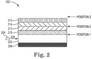
- FIG. 2 is a schematic cross-sectional view of embodiments of a backlight unit according to the present disclosure that indicates positions where a light conversion or light absorbing (blue-filtering) layer can be inserted.
- Backlight unit 200 includes light-guide plate 202 .
- a light-guide plate is a transparent, or semi-transparent colorless, block of material (glass or polymer) that can conduct light.
- Light-guide plates can be made of many materials such as glass, polyacrylate (acrylic), polycarbonate, or other clear polymers.
- Light-emitting diode array 204 arranged in a strip as a light source, can be arranged so that light 205 can enter backlight unit 200 through one edge of light-guide plate 202 .
- FIG. 1 is a schematic cross-sectional view of embodiments of a backlight unit according to the present disclosure that indicates positions where a light conversion or light absorbing (blue-filtering) layer can be inserted.
- Backlight unit 200 includes light-guide plate 202 .
- light-emitting diode array 204 can be located below light-guide plate 202 .
- Light-guide plate 202 can have reflector 206 adjacent to it on one or more sides in order to direct the light from light-emitting diode array 204 upward (as shown in FIG. 2 ) and through backlight unit 200 .
- light in backlight unit 200 can distribute itself uniformly through light-guide plate 202 through reflections from reflector 206 and internal reflections on the edges of light-guide plate 202 due to the refractive index difference between light-guide plate and air as well as reflection from the reflector and portions of the backlight unit yet to be described.
- the light-guide plate can be placed between a reflector layer between the reflector and the diffuser.
- the impact of this type of construction redirects light from the light source at the edge of a display screen uniformly across the display surface.
- the uniformity of the light distribution and the efficiency of the light collection are related to the efficiency of the light-guide plate, the reflector layer, and the diffuser layer or layers.
- Diffuser 216 can be disposed adjacent to light-guide plate 202 as shown in FIG. 2 .
- Diffuser 201 can evenly distribute light and eliminate bright spots.
- Diffusers can come in types, for example, such as holographic, white diffusing glass, and ground glass.
- Diffusers can be semi-opaque and can reflect light in many different directions.
- First brightness enhancing layer 213 and second brightness enhancing layer 214 can be prismatic brightness enhancing films. Prismatic brightness enhancing films are described earlier in this disclosure.
- Adjacent to second brightness enhancing layer 214 can be one or more polarizing filters 214 that lets light of a specific polarization pass through while blocking light waves of other polarizations.
- polarizing filters can help reduce reflections and glare by filtering out light that has become polarized due to reflection from non-metallic surfaces.
- the goal of backlight unit 200 is to distribute light uniformly across the two-dimensional plane of light-guide plate 202 , thus providing light to display images across the entirety of the display.
- the disclosed backlight unit with emission modification also includes an optical film, the optical film comprising at least one light conversion material or at least one light absorbing material or both.
- the light conversion material or light absorbing material can absorb light in a first wavelength range and reemit light in a second wavelength range having a higher wavelength.
- light conversion materials or light absorbing materials are contemplated that absorb blue light, particularly toxic blue light.
- Useful light conversion materials and light absorbing materials are described, for example, in applicants' co-owned U.S. patent application Ser. No. 15/813,010, currently allowed, filed Nov. 14, 2017 and entitled LIGHT EMISSION REDUCING COMPOUNDS FOR ELECTRONIC DEVICES.
- light 205 when light 205 is injected into light-guide plate 205 , it can reflect within light-guide plate 202 , from reflector 206 , from diffuser 216 , and from prismatic brightness enhancing layers 213 and 214 .
- Light 205 will necessarily eventually pass through the layers of backlight unit 200 multiple times and thus be distributed across the full area of a display located above the top layer of backlight unit 200 . This can create an opportunity to amplify the impact of a selective light conversion material or light absorbing material that filters out blue or toxic blue light or any other film or layer that can modify the spectrum.
- These selective light-conversion material or light absorbing material can be included as a separate film or can be coated onto any of the layers that make up the disclosed backlight unit.
- light-conversion materials placed in various locations in the backlight unit have been shown to have up to a ten to twelve times amplification of absorption which greatly increases the efficiency of selective light conversion material or light absorbing material that can, for example, filter out blue or toxic blue light.
- FIG. 3 shows the effective transmittance of the light-conversion or absorbing material (blue-light filtering layer) across the visible spectrum as a function of where the light conversion material or light conversion material is placed within the display backlight.
- the effective transmittance is calculated by dividing the emission from the display with the light conversion material or light absorbing material by the emission of the display without the light conversion material or light absorbing material.
- the different spectra shown in FIG. 3 illustrate the impact of the light conversion or light absorbing material layer when placed at different locations (positions) in the display—outside of and within the backlight unit.
- FIG. 3 are transmission spectra of different configurations of the embodiments shown in FIG. 2 with the light conversion or light absorbing material (blue-filtering) layer in the different positions as indicated in FIG. 2 . They show the transmission spectra of a typical backlight display configuration ( FIG. 2 ) with a layer of light conversion or light absorbing material positioned in three different places in the backlight filter.
- POSITION 1 the light conversion or light absorbing material was between light-guide plate 202 and diffuser 216 .
- POSITION 2 the light conversion or light absorbing material was between first prismatic brightness enhancing film 213 and second prismatic brightness enhancing film 214 .
- FIG. 1 is a schematic that shows a liquid crystal electronic imaging device on top of the backlight as disclosed above.
- the transmission spectrum shows very little absorption and reemission of light from the light-conversion material layer.
- the spectral line for POSITION 3 is relatively flat with few absorptions from the light-conversion material layer.
- the effect of the light-conversion or light absorbing material layer is shown in the middle curve of FIG. 3 .
- the transmission of light in the blue region of the spectrum 400 nm-500 nm
- the light-conversion material layer also has color balancing (color correction) ingredients that also decrease the red region of the spectrum (650 nm-700 nm) and also in the yellow portion of the spectrum (550 nm-615 nm).
- FIG. 4 are transmission spectra of embodiments of the backlight unit shown in FIG. 2 with the light-conversion layer in various positions in the backlight below the diffuser.
- the light-conversion layer was coated on a poly(ethylene terephthalate) (PET) film which was placed on the reflector, on the light-guide plate, and on the diffuser layer.
- PET poly(ethylene terephthalate)
- FIG. 4 shows three effective transmission curves of three different configurations of a backlight stack as illustrated in FIG. 2 .
- one curve is an absorption curve of the backlight unit shown if FIG. 2 with the light-conversion on PET layer positioned above the reflector and under the light-guide plate.
- a second absorption curve is a measurement of the spectrum of the same backlight unit with a light absorbing material on PET layer on top of the light-guide plate.
- the third absorption curve is the spectrum of the same backlight unit with the light-conversion on PET layer between the light-guide plate and the diffuser. It is the same as POSITION 1 on FIG. 2 .
- All three curves lie essentially on top of one another showing that having the light absorbing material layer located in any position below the prismatic brightness enhancing film does not substantially change the absorption and that the absorption of the backlight unit for all three configurations show the substantially the same amount of amplification of absorption with respect to the light absorbing material on top of the backlight unit.
Landscapes
- Physics & Mathematics (AREA)
- Nonlinear Science (AREA)
- General Physics & Mathematics (AREA)
- Optics & Photonics (AREA)
- Mathematical Physics (AREA)
- Chemical & Material Sciences (AREA)
- Crystallography & Structural Chemistry (AREA)
- Spectroscopy & Molecular Physics (AREA)
- Planar Illumination Modules (AREA)
Abstract
Description
-
- organic materials
- inorganic materials, which can be mined materials
- Raman-scattering materials
- Anti-Stokes materials
- materials known for other non-display applications, such as fingerprint dusting
- fluorescent pigments, such as those available from DayGlo Color Corp (for example, DAYGLO A-594-5). Surprisingly, materials that are used commonly in applications requiring florescent behavior can be used in light filtering applications with great spectral efficiency.
- luminescent nanocrystals such as SUNSTONE Luminescent UCP Nanocrystals available from Sigma Aldrich Co., LLC.
Claims (12)
Priority Applications (9)
| Application Number | Priority Date | Filing Date | Title |
|---|---|---|---|
| US17/177,920 US11126033B2 (en) | 2018-11-28 | 2021-02-17 | Backlight unit with emission modification |
| US17/348,570 US11592701B2 (en) | 2018-11-28 | 2021-06-15 | Backlight unit with emission modification |
| PCT/US2021/052904 WO2022177606A1 (en) | 2021-02-17 | 2021-09-30 | Backlight unit with emission modification |
| EP21857009.1A EP4070158A4 (en) | 2021-02-17 | 2021-09-30 | Backlight unit with emission modification |
| CN202180005599.6A CN115226403A (en) | 2021-02-17 | 2021-09-30 | Backlight unit with emission modification |
| KR1020227009105A KR20230143917A (en) | 2021-02-17 | 2021-09-30 | Backlight unit with emission modification function |
| JP2022520547A JP2023519464A (en) | 2021-02-17 | 2021-09-30 | Backlight unit that modifies light emission |
| US17/876,399 US20240036385A1 (en) | 2018-11-28 | 2022-07-28 | Color filter enhancements for display devices |
| US18/604,326 US20240219767A1 (en) | 2018-11-28 | 2024-03-13 | Color filter enhancements for display devices |
Applications Claiming Priority (4)
| Application Number | Priority Date | Filing Date | Title |
|---|---|---|---|
| US201862772513P | 2018-11-28 | 2018-11-28 | |
| US16/695,983 US10955697B2 (en) | 2018-11-28 | 2019-11-26 | Light emission modification |
| PCT/US2020/059308 WO2021108107A1 (en) | 2018-11-28 | 2020-11-06 | Light emission modification |
| US17/177,920 US11126033B2 (en) | 2018-11-28 | 2021-02-17 | Backlight unit with emission modification |
Related Parent Applications (3)
| Application Number | Title | Priority Date | Filing Date |
|---|---|---|---|
| US16/695,983 Continuation-In-Part US10955697B2 (en) | 2018-11-28 | 2019-11-26 | Light emission modification |
| PCT/US2020/059308 Continuation-In-Part WO2021108107A1 (en) | 2018-11-28 | 2020-11-06 | Light emission modification |
| US17/348,570 Continuation-In-Part US11592701B2 (en) | 2018-11-28 | 2021-06-15 | Backlight unit with emission modification |
Related Child Applications (2)
| Application Number | Title | Priority Date | Filing Date |
|---|---|---|---|
| US17/348,570 Continuation-In-Part US11592701B2 (en) | 2018-11-28 | 2021-06-15 | Backlight unit with emission modification |
| PCT/US2021/052904 Continuation-In-Part WO2022177606A1 (en) | 2018-11-28 | 2021-09-30 | Backlight unit with emission modification |
Publications (2)
| Publication Number | Publication Date |
|---|---|
| US20210165276A1 US20210165276A1 (en) | 2021-06-03 |
| US11126033B2 true US11126033B2 (en) | 2021-09-21 |
Family
ID=76091503
Family Applications (1)
| Application Number | Title | Priority Date | Filing Date |
|---|---|---|---|
| US17/177,920 Active US11126033B2 (en) | 2018-11-28 | 2021-02-17 | Backlight unit with emission modification |
Country Status (1)
| Country | Link |
|---|---|
| US (1) | US11126033B2 (en) |
Cited By (2)
| Publication number | Priority date | Publication date | Assignee | Title |
|---|---|---|---|---|
| US20220308391A1 (en) * | 2021-03-26 | 2022-09-29 | 3M Innovative Properties Company | Optical system with blue light absorbing layer |
| US12189237B2 (en) * | 2023-01-27 | 2025-01-07 | Lg Display Co., Ltd. | Display device |
Families Citing this family (4)
| Publication number | Priority date | Publication date | Assignee | Title |
|---|---|---|---|---|
| US10642087B2 (en) | 2014-05-23 | 2020-05-05 | Eyesafe, Llc | Light emission reducing compounds for electronic devices |
| US11810532B2 (en) | 2018-11-28 | 2023-11-07 | Eyesafe Inc. | Systems for monitoring and regulating harmful blue light exposure from digital devices |
| US11592701B2 (en) | 2018-11-28 | 2023-02-28 | Eyesafe Inc. | Backlight unit with emission modification |
| US11428987B2 (en) * | 2020-05-22 | 2022-08-30 | Apple Inc. | Electronic device display with a backlight having light-emitting diodes and driver integrated circuits in an active area |
Citations (212)
| Publication number | Priority date | Publication date | Assignee | Title |
|---|---|---|---|---|
| US2403685A (en) | 1941-03-31 | 1946-07-09 | Rca Corp | Light filter |
| US2493200A (en) | 1946-05-31 | 1950-01-03 | Polaroid Corp | Variable polarizing color filter |
| US3382183A (en) | 1965-09-02 | 1968-05-07 | American Cyanamid Co | Plastic optical filter |
| US3482915A (en) | 1967-03-21 | 1969-12-09 | Ferrand D E Corley | Colour film reproducing system |
| US3687863A (en) | 1970-05-25 | 1972-08-29 | Gen Telephone & Elect | Optical filters containing tetraphenyl-porphins and method of making same |
| US4618216A (en) | 1980-03-24 | 1986-10-21 | Seiko Epson Kabushiki Kaisha | Backlighted liquid crystal display using light passage member for more nearly uniform illumination |
| WO1988002871A1 (en) | 1986-10-16 | 1988-04-21 | Suntiger, Incorporated | Ultraviolet radiation and blue light blocking polarizing lens |
| US4842781A (en) | 1984-02-29 | 1989-06-27 | Mitsui Toatsu Chemicals, Inc. | Colored polarizing film and method of making same |
| US4878748A (en) | 1987-02-26 | 1989-11-07 | Suntiger, Inc. | Ultraviolet radiation and blue light blocking polarizing lens |
| US4966441A (en) | 1989-03-28 | 1990-10-30 | In Focus Systems, Inc. | Hybrid color display system |
| US4989953A (en) | 1989-01-24 | 1991-02-05 | Kirschner Kevin A | Video display terminal filter |
| US5083252A (en) | 1990-04-19 | 1992-01-21 | Tailored Lighting Company, Inc. | Apparatus for producing light distributions |
| EP0509727A2 (en) | 1991-04-10 | 1992-10-21 | Sharp Kabushiki Kaisha | Liquid crystal display device |
| US5177509A (en) | 1987-02-26 | 1993-01-05 | Suntiger, Inc. | Ultraviolet radiation and blue light blocking polarizing lens |
| US5483464A (en) | 1993-03-31 | 1996-01-09 | Samsung Electronics Co., Ltd. | Power saving apparatus for use in peripheral equipment of a computer |
| US5555492A (en) | 1992-08-31 | 1996-09-10 | Itt Automotive Europe Gmbh | Signal lamp |
| US5745391A (en) | 1995-09-13 | 1998-04-28 | Topor; Yakov | Apparatus for and method of turning on and shutting off a computing device |
| EP0855602A2 (en) | 1997-01-28 | 1998-07-29 | Kyowa Hakko Kogyo Co., Ltd. | Molded synthetic resin |
| US5952096A (en) | 1996-01-26 | 1999-09-14 | Teijin Chemicals, Ltd. | Spectacle lens |
| US6019476A (en) | 1996-06-24 | 2000-02-01 | Kirschner; Kevin A. | Full spectrum filtering for fluorescent lighting |
| US6229252B1 (en) | 1999-01-21 | 2001-05-08 | Asahi Glass Company, Limited | Dye combinations for multiple bandpass filters for video displays |
| JP2001315240A (en) | 2000-05-02 | 2001-11-13 | Bridgestone Corp | Electromagnetic wave shielding light pervious laminated film and display panel |
| US20020005509A1 (en) | 1999-01-21 | 2002-01-17 | Chia-Chi Teng | Dye combinations for image enhancement filters for color video displays |
| US20020018890A1 (en) | 2000-02-14 | 2002-02-14 | Bridgestone Corporation | Optical filter and plasma display panel |
| US20020158574A1 (en) | 2001-04-27 | 2002-10-31 | 3M Innovative Properties Company | Organic displays and devices containing oriented electronically active layers |
| WO2002101695A1 (en) | 2001-06-12 | 2002-12-19 | Mitsubishi Chemical Corporation | Electronic display-use filter and electronic display unit using the filter |
| JP2003149605A (en) | 2001-11-16 | 2003-05-21 | Nippon Sheet Glass Co Ltd | Anti-glare optical article |
| US20030214695A1 (en) | 2002-03-18 | 2003-11-20 | E Ink Corporation | Electro-optic displays, and methods for driving same |
| US6663978B1 (en) | 2000-06-28 | 2003-12-16 | 3M Innovative Properties Company | High refractive index pressure-sensitive adhesives |
| US20040070726A1 (en) | 2000-11-03 | 2004-04-15 | Andrew Ishak | Waterman's sunglass lens |
| US20040114242A1 (en) | 2002-09-06 | 2004-06-17 | Sharp Gary D. | Filter for enhancing vision and/or protecting the eyes and method of making a filter |
| US6778238B2 (en) | 2001-02-14 | 2004-08-17 | Lg. Philips Lcd Co., Ltd. | Reflective liquid crystal display device using a cholesteric liquid crystal color filter |
| US20040166342A1 (en) | 2003-02-25 | 2004-08-26 | Degussa Ag | Transparent molding composition for optical applications |
| US20040181006A1 (en) | 2003-03-14 | 2004-09-16 | Warren Leslie F. | Composition for filter material |
| WO2004090589A1 (en) | 2003-04-14 | 2004-10-21 | Ingo Uckermann | Film, particularly a sun protection film, and production and use thereof |
| US6826001B2 (en) | 2001-02-23 | 2004-11-30 | Dainippon Ink And Chemicals, Inc. | Color filter |
| US6824712B1 (en) | 1999-08-04 | 2004-11-30 | Skc Co. Ltd. | Selectively light-absorptive material, coating composition containing the same, and filter manufactured using the coating composition for color displays |
| US20040246413A1 (en) | 2003-06-05 | 2004-12-09 | Eastman Kodak Company | UV curable conductive materials in displays |
| US6846579B2 (en) | 2002-02-15 | 2005-01-25 | Eastman Kodak Company | Multilayer with radiation absorber and touch screen |
| US20050042531A1 (en) | 2003-08-19 | 2005-02-24 | Yeon-Keun Lee | Film for plasma display filter and plasma display filter comprising the same |
| WO2005034066A1 (en) | 2003-09-30 | 2005-04-14 | Mitsubishi Chemical Corporation | Electronic display filter and electronic display device |
| US6955430B2 (en) | 2001-12-11 | 2005-10-18 | Pratt Steven G | Blue blocking lens |
| WO2005106542A1 (en) | 2004-04-30 | 2005-11-10 | Ace Digitech, Ltd. | Dye and optical film for flat panel display device |
| US20050259082A1 (en) | 2002-08-13 | 2005-11-24 | Fujitsu Siemens Computers Gmbh | Display device |
| US20050275769A1 (en) | 2004-06-11 | 2005-12-15 | Nam-Seok Roh | Liquid crystal display device |
| US20060012754A1 (en) | 2004-07-14 | 2006-01-19 | Larson Brent D | Color correcting contrast enhancement of displays |
| US6991849B2 (en) | 2001-06-21 | 2006-01-31 | Teijin Limited | Near infrared ray shielding film |
| JP2006031030A (en) | 2005-07-22 | 2006-02-02 | Kyowa Hakko Kogyo Co Ltd | Synthetic resin molding |
| US7014336B1 (en) | 1999-11-18 | 2006-03-21 | Color Kinetics Incorporated | Systems and methods for generating and modulating illumination conditions |
| US7019903B2 (en) | 2001-03-26 | 2006-03-28 | Andreas Berger | Color dichroic polarizers and method for the production thereof |
| US7019799B2 (en) | 2001-02-09 | 2006-03-28 | Hitachi, Ltd. | Liquid crystal display with optical adjustment layer controlling transmittance of emitted light in accordance with wavelength |
| US7019331B2 (en) | 2004-01-22 | 2006-03-28 | Eastman Kodak Company | Green light-emitting microcavity OLED device using a yellow color filter element |
| US7045944B2 (en) | 2002-08-26 | 2006-05-16 | Hitachi Displays, Ltd. | Image display apparatus with ultraviolet ray shield resin film and process for its production |
| KR20060048986A (en) | 2004-08-28 | 2006-05-18 | 주식회사 엘지화학 | Film for PD filter, PD filter including same and plasma display panel manufactured using said PD filter |
| US7066596B2 (en) | 2001-11-02 | 2006-06-27 | Andrew Ishak | Rugate lens for glasses |
| US7071602B2 (en) | 2001-04-27 | 2006-07-04 | Asahi Glass Company, Limited | Filter for plasma display panel |
| US7126589B2 (en) | 2002-05-29 | 2006-10-24 | Au Optronics Corporation | Touch control panel |
| US7158300B2 (en) | 2002-07-24 | 2007-01-02 | Sony Corporation | Projection screen and its manufacturing method |
| US20070013649A1 (en) * | 2005-07-14 | 2007-01-18 | Samsung Electronics Co., Ltd. | Electrophoretic display device with improved reflective luminance |
| US7193779B2 (en) | 2003-02-12 | 2007-03-20 | Lg Electronics Inc. | Front filter in plasma display panel |
| US20070077410A1 (en) | 2005-09-30 | 2007-04-05 | Guangda Shi | Plastic films |
| US20070078216A1 (en) | 2005-09-30 | 2007-04-05 | Feng Cao | Plastic compositions and products produced therefrom |
| US7218044B2 (en) | 2003-02-12 | 2007-05-15 | Lg Electronics Inc. | Front filter in plasma display panel |
| EP0965034B1 (en) | 1997-03-07 | 2007-05-30 | Clare Chemical Research, Inc. | Fluorometric detection using visible light |
| WO2007075520A2 (en) | 2005-12-16 | 2007-07-05 | Andrew Ishak | Ophthalmic lens to preserve macular integrity |
| US7258923B2 (en) | 2003-10-31 | 2007-08-21 | General Electric Company | Multilayered articles and method of manufacture thereof |
| US20070195404A1 (en) | 2004-03-10 | 2007-08-23 | Tomohiko Iijima | Transparent laminate |
| US20070216861A1 (en) | 2006-03-20 | 2007-09-20 | Andrew Ishak | Ophthalmic system combining ophthalmic components with blue light wavelength blocking and color-balancing functionalities |
| US20070275184A1 (en) | 2006-05-23 | 2007-11-29 | Byoung Hoo Lee | Optical film, optical filter and display device including the same |
| WO2007146933A2 (en) | 2006-06-12 | 2007-12-21 | High Performance Optics, Inc. | Color balanced ophthalmic system with selective light inhibition |
| WO2008024414A2 (en) | 2006-08-23 | 2008-02-28 | High Performance Optics, Inc. | System and method for selective light inhibition |
| CA2924278A1 (en) | 2006-11-28 | 2008-06-05 | High Performance Optics, Inc. | High performance selective light wavelength filtering providing improved contrast sensitivity |
| WO2008067109A1 (en) | 2006-11-28 | 2008-06-05 | High Performance Optics, Inc. | High performance selective light wavelength filtering providing improved contrast sensitivity |
| US20080137030A1 (en) | 2006-11-03 | 2008-06-12 | Hoffman William C | Optical devices with reduced chromatic aberration |
| WO2008068353A1 (en) | 2006-12-04 | 2008-06-12 | Universidad Complutense De Madrid | Component for prevention purposes in healthy eyes and for treatment and prophylaxis in pseudo-aphacic eyes and/or eyes affected by neurodegenerative processes |
| FR2909779A1 (en) | 2006-12-08 | 2008-06-13 | Gestion De Marques Sogema Soci | GLASSES TO REDUCE VISUAL FATIGUE |
| CN101216611A (en) | 2007-12-31 | 2008-07-09 | 曾琪 | Blue ray radiation preventing and achromatism spectacle lens, and method of producing the same |
| WO2008106449A1 (en) | 2007-02-26 | 2008-09-04 | High Performance Optics, Inc. | High performance corneal inlay |
| US20080290787A1 (en) | 2007-05-21 | 2008-11-27 | Cok Ronald S | Device and method for improved power distribution for a transparent electrode |
| US20080297931A1 (en) | 2007-06-01 | 2008-12-04 | Universidad Complutense De Madrid | Element for use on the transparent surfaces of buildings for eye protection and therapy |
| US7491440B2 (en) | 2003-12-26 | 2009-02-17 | Sekisui Chemical Co., Ltd. | Interlayer film for laminate glass and laminate glass |
| US20090058250A1 (en) | 2007-08-29 | 2009-03-05 | Samsung Corning Precision Glass Co., Ltd. | Filter for display apparatus |
| US7520608B2 (en) | 2006-03-20 | 2009-04-21 | High Performance Optics, Inc. | Color balanced ophthalmic system with selective light inhibition |
| US20090105437A1 (en) | 2007-10-19 | 2009-04-23 | 3M Innovative Properties Company | High refractive index pressure-sensitive adhesives |
| US7524060B2 (en) | 2005-04-19 | 2009-04-28 | Universidad Complutense De Madrid | Therapeutic contact lens for pseudo-aphakic eyes and/or eyes with retinal neuro-degeneration |
| US20090128895A1 (en) | 2007-11-20 | 2009-05-21 | Samsung Corning Precision Glass Co., Ltd. | Filter for display device |
| EP2085798A1 (en) | 2006-10-16 | 2009-08-05 | Universidad Complutense De Madrid | Lighting device with prophylactic and therapeutic filter for healthy eyes, pseudoaphakic eyes and/or eyes suffering neurodegeneration |
| US7572028B2 (en) | 1999-11-18 | 2009-08-11 | Philips Solid-State Lighting Solutions, Inc. | Methods and apparatus for generating and modulating white light illumination conditions |
| US7579769B2 (en) | 2002-10-18 | 2009-08-25 | Ifire Ip Corporation | Color electroluminescent displays including photoluminescent phosphor layer |
| WO2009123754A2 (en) | 2008-04-04 | 2009-10-08 | High Performance Optics, Inc. | Dual-filter ophthalmic lens to reduce risk of macular degeneration |
| EP2128889A1 (en) | 2007-02-07 | 2009-12-02 | Universidad Complutense de Madrid Rectorado | Light source with reduced emission of short wavelengths for protection of the eyes |
| US20100039704A1 (en) * | 2006-10-27 | 2010-02-18 | Hideki Hayashi | Prism sheet and optical sheet |
| US7695180B2 (en) | 2005-08-27 | 2010-04-13 | 3M Innovative Properties Company | Illumination assembly and system |
| US7703917B2 (en) | 2006-01-10 | 2010-04-27 | Universidad Complutense De Madrid | Therapeutic prophylactic ophthalmologic lens for pseudoaphakic eyes and/or eyes suffering neurodegeneration |
| US20100134879A1 (en) | 2007-04-26 | 2010-06-03 | Masanori Yoshihara | Display screen protection film and polarization plate |
| US7731791B2 (en) | 2004-10-01 | 2010-06-08 | Ciba Specialty Chemicals Corporation | Use of pyrimido[5,4-g]pteridines as shading component in color filter colorant compositions |
| US7755276B2 (en) | 2005-01-14 | 2010-07-13 | Intematix Corporation | Aluminate-based green phosphors |
| US7785501B2 (en) | 2004-12-28 | 2010-08-31 | Dai Nippon Printing Co., Ltd. | Black resin composition for display device, and member for display device |
| US20100231830A1 (en) | 2006-02-28 | 2010-09-16 | Fujifilm Corporation | Polarizing plate and liquid crystal display |
| WO2010111499A1 (en) | 2009-03-25 | 2010-09-30 | High Performance Optics, Inc. | Photochromic ophthalmic systems that selectively filter specific blue light wavelengths |
| US7825578B2 (en) | 2006-03-01 | 2010-11-02 | Nichia Corporation | Yellow light emitting device with high luminance |
| US7832903B2 (en) | 2006-11-07 | 2010-11-16 | Universidad Complutense De Madrid | Illumination system fitted with a therapeutic/prophylactic filter for healthy eyes, pseudoaphakic eyes or eyes suffering neurodegeneration |
| JP2010261986A (en) | 2009-04-30 | 2010-11-18 | Bridgestone Corp | Method for forming dye-containing layer for optical filter, optical film having dye-containing layer formed by the method, and optical filter for display |
| CN101899222A (en) | 2010-07-01 | 2010-12-01 | 北川天诺光电材料有限公司 | Neon yellow light absorbing dye and application thereof |
| CN201666985U (en) | 2010-04-09 | 2010-12-08 | 厦门虹泰光学有限公司 | Blue-light resistant eyeglass |
| US20110019269A1 (en) | 2009-07-21 | 2011-01-27 | Board Of Regents Of The University Of Texas System | Protective Light Filters Having Customized Spectral Profiles |
| US20110043486A1 (en) | 2009-08-20 | 2011-02-24 | Toppan Printing Co., Ltd. | Liquid crystal display device, black matrix substrate and color filter substrate |
| US7914177B2 (en) | 2006-11-07 | 2011-03-29 | Universidad Complutense De Madrid | Prophylaxic/therapeutic vehicle filter component for healthy eyes, pseudoaphakic eyes or eyes suffering neurodegeneration |
| US20110176325A1 (en) | 2008-07-10 | 2011-07-21 | 3M Innovative Properties Company | Viscoelastic lightguide |
| JP2011144280A (en) | 2010-01-15 | 2011-07-28 | Adeka Corp | Color tone-correcting agent, squarylium compound, and optical filter |
| US20110234079A1 (en) | 2010-03-29 | 2011-09-29 | Samsung Electronics Co. Ltd. | Polarizer and organic electroluminescent device having the same |
| US8034206B2 (en) | 2008-04-29 | 2011-10-11 | Samsung Electronics Co., Ltd. | Method of fabricating flexible display device |
| US8044942B1 (en) | 2011-01-18 | 2011-10-25 | Aevoe Inc. | Touch screen protector |
| US8063999B2 (en) | 2007-04-13 | 2011-11-22 | Okamoto Glass Co., Ltd. | Glass polarizer and manufacturing method thereof |
| US20110289654A1 (en) | 2010-05-29 | 2011-12-01 | Thomas Lovell Williams | Electrically conductive device to be applied to a portion of a glove for use with touch screen device |
| US20110299168A1 (en) | 2010-06-04 | 2011-12-08 | Combs Jeffrey S | Display Screen Covers Having Personalized Refractive Power Capabilities |
| US8075133B2 (en) | 2007-07-19 | 2011-12-13 | Universidad Complutense De Madrid | Safety helmet visor with a treated surface for eye protection and therapy |
| US8075145B2 (en) | 2010-03-05 | 2011-12-13 | Engblom James A | Display screen shades for mobile devices |
| US20110315939A1 (en) | 2009-02-20 | 2011-12-29 | Japan Carlit Co., Ltd. | Near infrared absorbent dye and near infrared shielding filter |
| WO2012006265A1 (en) | 2010-07-06 | 2012-01-12 | High Performance Optics, Inc. | High energy visible light filter systems with yellowness index values |
| US20120021152A1 (en) | 2009-02-12 | 2012-01-26 | Basf Se | Polymer compositions containing nanoparticulate ir absorbers |
| US8113651B2 (en) | 2006-03-20 | 2012-02-14 | High Performance Optics, Inc. | High performance corneal inlay |
| US20120038861A1 (en) | 2010-08-12 | 2012-02-16 | Polymer Vision B.V. | Electronic Display Comprising An Adjustable Color Filter |
| US20120075577A1 (en) | 2006-03-20 | 2012-03-29 | Ishak Andrew W | High performance selective light wavelength filtering providing improved contrast sensitivity |
| US8164844B2 (en) | 2005-03-16 | 2012-04-24 | Panasonic Corporation | Optical filter and lighting apparatus |
| US20120162106A1 (en) | 2010-12-28 | 2012-06-28 | Lg Electronics Inc. | Window, fabricating method thereof and mobile terminal having the same |
| US20120162752A1 (en) | 2009-08-24 | 2012-06-28 | Hirofumi Kitano | Intermediate film for laminated glass, and laminated glass |
| US8303859B2 (en) | 2007-12-24 | 2012-11-06 | Cheil Industries, Inc. | Optical film for suppressing near infrared ray transmittance and display filter using the same |
| US8323357B2 (en) | 2009-04-15 | 2012-12-04 | Lanxess Deutschland Gmbh | Fluorine-substituted perylenes for colour filters in LCDS |
| US20130009059A1 (en) | 2007-03-26 | 2013-01-10 | Nunzio Giuseppe Caruso | Device for increased eye protection |
| CN102879920A (en) | 2012-10-11 | 2013-01-16 | 傅雯 | Special goggle lens for youngsters to prevent electronic luminescent screen hurts |
| US8360574B2 (en) | 2006-03-20 | 2013-01-29 | High Performance Optics, Inc. | High performance selective light wavelength filtering providing improved contrast sensitivity |
| US20130063493A1 (en) | 2011-09-14 | 2013-03-14 | Htc Corporation | Devices and Methods Involving Display Interaction Using Photovoltaic Arrays |
| CN202847016U (en) | 2012-10-16 | 2013-04-03 | 山太士股份有限公司 | UV anti-viscosity protective film |
| JP2013067811A (en) | 2012-12-06 | 2013-04-18 | Adeka Corp | Light-shielding film |
| JP2013524300A (en) | 2010-04-15 | 2013-06-17 | オークリー インコーポレイテッド | Eyewear with enhanced saturation |
| US8498042B2 (en) | 2007-01-22 | 2013-07-30 | E Ink Corporation | Multi-layer sheet for use in electro-optic displays |
| US8507840B2 (en) | 2010-12-21 | 2013-08-13 | Zena Technologies, Inc. | Vertically structured passive pixel arrays and methods for fabricating the same |
| US8506114B2 (en) | 2007-02-22 | 2013-08-13 | Cree, Inc. | Lighting devices, methods of lighting, light filters and methods of filtering light |
| US8518498B2 (en) | 2009-09-02 | 2013-08-27 | Samsung Display Co., Ltd. | Liquid crystal display and manufacturing method thereof |
| WO2013123592A1 (en) | 2012-02-23 | 2013-08-29 | Switch Materials Inc. | Optical filter with light source |
| US20130239874A1 (en) | 2012-03-15 | 2013-09-19 | Temptime Corporation | Robust, ultraviolet-protected ambient condition history indicator and method of making same |
| US8547504B2 (en) | 2010-04-27 | 2013-10-01 | The Regents Of The University Of Michigan | Display device having plasmonic color filters and photovoltaic capabilities |
| US8570648B2 (en) | 2007-10-15 | 2013-10-29 | Universidad Complutense De Madrid | Material for covering, coating or screening for eye protection and therapy against the effects of blue light |
| JP2013238634A (en) | 2012-05-11 | 2013-11-28 | Ito Kogaku Kogyo Kk | Anti-glare optical element |
| WO2013176888A1 (en) | 2012-05-22 | 2013-11-28 | Aevoe Corp. | Touch screen protector |
| ES1094781U (en) | 2013-06-03 | 2013-12-03 | Universidad Complutense De Madrid | Diopter configured to restrict electromagnetic radiation that damages the visual system (Machine-translation by Google Translate, not legally binding) |
| US8599542B1 (en) | 2013-05-17 | 2013-12-03 | Zagg Intellectual Property Holding Co., Inc. | Combined cover, keyboard and stand for tablet computer with reversable connection for keyboard and reading configuration |
| CN103448312A (en) | 2013-09-10 | 2013-12-18 | 温志光 | Screen protection film capable of filtering blue light and preparation method of screen protection film |
| WO2013188825A1 (en) | 2012-06-15 | 2013-12-19 | The Regents Of The University Of California | Optical filters and methods for reducing glare from glare-producing light |
| JP2014000819A (en) | 2013-08-03 | 2014-01-09 | Mitsubishi Plastics Inc | Laminated polyester film |
| CN203410122U (en) | 2013-06-28 | 2014-01-29 | 典佑科技有限公司 | Screen protection paste for filtering blue light |
| US20140049700A1 (en) | 2012-08-15 | 2014-02-20 | Au Optronics Corp. | Optical touch display device and color filter thereof |
| DE202014000982U1 (en) | 2013-02-07 | 2014-03-12 | Dian-You Technology Co., Ltd. | Screen protector with the function of a blue light filter |
| US20140078420A1 (en) | 2012-08-17 | 2014-03-20 | Shanghai Tianma Micro-electronics Co., Ltd. | In-cell touch panel and color filter substrate thereof |
| US8680406B2 (en) | 2011-09-07 | 2014-03-25 | Trend Power Limited | Radiation-proof laminate for electronic devices and method for embedding the same into a case |
| US8680492B2 (en) | 2011-05-19 | 2014-03-25 | Shenzhen China Star Optoelectronics Technology Co., Ltd. | Light guide plate and backlight module utilizing ultraviolet light source |
| US20140093661A1 (en) | 2012-10-02 | 2014-04-03 | High Performance Optics, Inc. | Selective Blue Light Filtered Optic |
| WO2014055513A1 (en) | 2012-10-02 | 2014-04-10 | High Performance Optics, Inc. | Selective blue light filtered optic |
| US8716729B2 (en) | 2007-12-21 | 2014-05-06 | Osram Opto Semiconductors Gmbh | Lighting device |
| WO2014077166A1 (en) | 2012-11-14 | 2014-05-22 | 旭硝子株式会社 | Optical filter |
| WO2014096475A1 (en) | 2012-12-21 | 2014-06-26 | Universidad Complutense De Madrid | Element for blocking short wavelengths in led-type light sources |
| US8767282B2 (en) | 2009-11-06 | 2014-07-01 | Sharp Laboratories Of America, Inc. | Plasmonic in-cell polarizer |
| CN103941320A (en) | 2014-04-08 | 2014-07-23 | 丁鹏飞 | Device for selectively filtering light rays |
| US20140233105A1 (en) | 2011-03-03 | 2014-08-21 | Enchroma, Inc. | Multi-band color vision filters and method by lp-optimization |
| US8817207B2 (en) | 2008-10-13 | 2014-08-26 | Samsung Display Co., Ltd. | Liquid crystal display with UV or blue light blocking filter |
| US8836209B2 (en) | 2011-07-15 | 2014-09-16 | Samsung Display Co., Ltd. | Display apparatus |
| WO2014155787A1 (en) | 2013-03-29 | 2014-10-02 | 積水化成品工業株式会社 | Optical film |
| US20140355106A1 (en) | 2011-12-22 | 2014-12-04 | Saint-Gobain Glass France | Device for viewing an image on a laminated substrate |
| US20140363767A1 (en) | 2011-12-05 | 2014-12-11 | Hitachi Chemical Company, Ltd. | Method for forming resin cured film pattern, photosensitive resin composition, photosensitive element, method for producing touch panel, and resin cured film |
| WO2014196638A1 (en) | 2013-06-06 | 2014-12-11 | 富士フイルム株式会社 | Optical sheet member and image display device using same |
| US8928220B2 (en) | 2012-04-23 | 2015-01-06 | Samsung Electronics Co., Ltd. | White light emitting device and display apparatus |
| US8957835B2 (en) | 2008-09-30 | 2015-02-17 | Apple Inc. | Head-mounted display apparatus for retaining a portable electronic device with display |
| US8982197B2 (en) | 2009-02-03 | 2015-03-17 | Lg Chem, Ltd. | Optical filter |
| CN204213761U (en) * | 2014-12-03 | 2015-03-18 | 福建捷联电子有限公司 | A kind of display backlight structure reducing blue light harm |
| US20150098058A1 (en) | 2012-05-16 | 2015-04-09 | Essilor International (Compagnie Generale- D'optique) | Ophthalmic lens |
| US20150124188A1 (en) * | 2012-05-28 | 2015-05-07 | Sharp Kabushiki Kaisha | Color-converting substrate and liquid crystal display device |
| CN104614786A (en) | 2013-11-01 | 2015-05-13 | 佑顺发机械股份有限公司 | Optical film with blue light suppression function |
| EP2874001A1 (en) | 2013-11-18 | 2015-05-20 | EverDisplay Optronics (Shanghai) Limited | Flat-panel display and method for making the same |
| US9051232B2 (en) | 2008-12-01 | 2015-06-09 | Canon Kabushiki Kaisha | Perylene compound and organic light emitting device using the compound |
| US20150212238A1 (en) | 2014-01-28 | 2015-07-30 | Bing-Chen Chang | Screen protection sheet with function of blue light filtering |
| US20150212352A1 (en) | 2013-04-09 | 2015-07-30 | Boe Technology Group Co., Ltd. | Liquid crystal display panel, display device and process for patterning quantum dot layer |
| US9122089B2 (en) | 2010-06-10 | 2015-09-01 | Samsung Display Co., Ltd. | Display device |
| US20150248033A1 (en) * | 2012-09-14 | 2015-09-03 | Apple, Inc. | Displays With Elevated Backlight Efficiency |
| US20150253653A1 (en) | 2012-09-18 | 2015-09-10 | Kazuhiro Fujita | Illumination device, projector, and illumination method |
| CN104950515A (en) | 2014-03-31 | 2015-09-30 | 冠捷投资有限公司 | Display panel with short-wave blue light inhibition function |
| WO2015179761A1 (en) | 2014-05-23 | 2015-11-26 | Digihealth LLC | Light emission reducing film for electronic devices |
| US20150378217A1 (en) * | 2014-06-25 | 2015-12-31 | Samsung Display Co., Ltd. | Fluorescent sheet and light unit and liquid crystal display including the same |
| US9287471B2 (en) | 2012-02-29 | 2016-03-15 | Sabic Global Technologies B.V. | Polycarbonate compositions containing conversion material chemistry and having enhanced optical properties, methods of making and articles comprising the same |
| KR20160066707A (en) | 2014-12-03 | 2016-06-13 | 에스케이씨하스디스플레이필름(유) | Blue light cut protective film |
| US9377569B2 (en) | 2006-03-20 | 2016-06-28 | High Performance Optics, Inc. | Photochromic ophthalmic systems that selectively filter specific blue light wavelengths |
| JP2016126064A (en) | 2014-12-26 | 2016-07-11 | 旭硝子株式会社 | Filter and liquid crystal display device |
| CN105788474A (en) | 2014-12-24 | 2016-07-20 | 北京维信诺科技有限公司 | LED backlight liquid crystal display capable of reducing blue light hazard |
| WO2016205260A1 (en) | 2015-06-15 | 2016-12-22 | Healthe Llc | Light emission reducing compounds for electronic devices |
| CN106324908A (en) | 2016-10-12 | 2017-01-11 | 深圳市华星光电技术有限公司 | Liquid crystal display device |
| US9575335B1 (en) | 2014-01-10 | 2017-02-21 | Oakley, Inc. | Eyewear with chroma enhancement for specific activities |
| WO2017039024A1 (en) | 2015-08-28 | 2017-03-09 | 주식회사 쏠컴포넌트 | Light-emitting diode module having colour mixing and blue-light blocking functions, and lighting apparatus including same |
| US9798163B2 (en) | 2013-05-05 | 2017-10-24 | High Performance Optics, Inc. | Selective wavelength filtering with reduced overall light transmission |
| US20170309235A1 (en) | 2014-09-15 | 2017-10-26 | Tecnología Sostenible Y Responsable Sl | Method and portable electronic device having a double screen |
| US20170363884A1 (en) | 2014-12-05 | 2017-12-21 | 3M Innovative Properties Company | Vision-protecting filter lens |
| KR101815619B1 (en) | 2016-11-30 | 2018-01-05 | 삼성전자주식회사 | White light emitting diode, backlight unit, and liquid crystal display including the same |
| US20180052362A1 (en) * | 2016-08-22 | 2018-02-22 | Samsung Display Co., Ltd. | Liquid crystal display device and manufacturing method of the same |
| US20180107050A1 (en) | 2014-05-23 | 2018-04-19 | Healthe, LLC | Light emission reducing compounds for electronic devices |
| US20190004223A1 (en) | 2015-07-29 | 2019-01-03 | Tecnología Sostenible Y Responsable Sl | Refractive surface for blocking short- and medium- wavelength visible-spectrum radiation that affects human physiology |
| US20190121176A1 (en) * | 2017-10-25 | 2019-04-25 | Samsung Display Co., Ltd. | Color conversion element and display device including the same |
| WO2019099554A1 (en) | 2017-11-14 | 2019-05-23 | Healthe Llc | Light emission reducing compounds for electronic devices |
| CN209782327U (en) | 2019-03-19 | 2019-12-13 | 天津浩清节能科技有限公司 | Eye-protecting lamp convenient to adjust light-emitting angle and capable of reducing blue light damage |
| US20200124781A1 (en) | 2018-10-22 | 2020-04-23 | Unique Materials Co., Ltd. | Light conversion layer, backlight module, and display device including the same |
| US10649129B2 (en) | 2017-05-16 | 2020-05-12 | Shenzhen China Star Optoelectronics Technology Co., Ltd | Light guide plate, backlight module and display device |
| US20200166798A1 (en) | 2018-11-28 | 2020-05-28 | Eyesafe, Llc | Light emission modification |
| US20200303598A1 (en) | 2019-03-22 | 2020-09-24 | Samsung Electronics Co., Ltd. | White light emitting module |
| US20210043807A1 (en) | 2019-08-09 | 2021-02-11 | Eyesafe, Llc | White led light source and method of making same |
-
2021
- 2021-02-17 US US17/177,920 patent/US11126033B2/en active Active
Patent Citations (249)
| Publication number | Priority date | Publication date | Assignee | Title |
|---|---|---|---|---|
| US2403685A (en) | 1941-03-31 | 1946-07-09 | Rca Corp | Light filter |
| US2493200A (en) | 1946-05-31 | 1950-01-03 | Polaroid Corp | Variable polarizing color filter |
| US3382183A (en) | 1965-09-02 | 1968-05-07 | American Cyanamid Co | Plastic optical filter |
| US3482915A (en) | 1967-03-21 | 1969-12-09 | Ferrand D E Corley | Colour film reproducing system |
| US3687863A (en) | 1970-05-25 | 1972-08-29 | Gen Telephone & Elect | Optical filters containing tetraphenyl-porphins and method of making same |
| US4618216A (en) | 1980-03-24 | 1986-10-21 | Seiko Epson Kabushiki Kaisha | Backlighted liquid crystal display using light passage member for more nearly uniform illumination |
| US4842781A (en) | 1984-02-29 | 1989-06-27 | Mitsui Toatsu Chemicals, Inc. | Colored polarizing film and method of making same |
| WO1988002871A1 (en) | 1986-10-16 | 1988-04-21 | Suntiger, Incorporated | Ultraviolet radiation and blue light blocking polarizing lens |
| US4878748A (en) | 1987-02-26 | 1989-11-07 | Suntiger, Inc. | Ultraviolet radiation and blue light blocking polarizing lens |
| US5177509A (en) | 1987-02-26 | 1993-01-05 | Suntiger, Inc. | Ultraviolet radiation and blue light blocking polarizing lens |
| US4989953A (en) | 1989-01-24 | 1991-02-05 | Kirschner Kevin A | Video display terminal filter |
| US4966441A (en) | 1989-03-28 | 1990-10-30 | In Focus Systems, Inc. | Hybrid color display system |
| US5083252A (en) | 1990-04-19 | 1992-01-21 | Tailored Lighting Company, Inc. | Apparatus for producing light distributions |
| EP0509727A2 (en) | 1991-04-10 | 1992-10-21 | Sharp Kabushiki Kaisha | Liquid crystal display device |
| US5555492A (en) | 1992-08-31 | 1996-09-10 | Itt Automotive Europe Gmbh | Signal lamp |
| US5483464A (en) | 1993-03-31 | 1996-01-09 | Samsung Electronics Co., Ltd. | Power saving apparatus for use in peripheral equipment of a computer |
| US5745391A (en) | 1995-09-13 | 1998-04-28 | Topor; Yakov | Apparatus for and method of turning on and shutting off a computing device |
| US5952096A (en) | 1996-01-26 | 1999-09-14 | Teijin Chemicals, Ltd. | Spectacle lens |
| US6019476A (en) | 1996-06-24 | 2000-02-01 | Kirschner; Kevin A. | Full spectrum filtering for fluorescent lighting |
| EP0855602A2 (en) | 1997-01-28 | 1998-07-29 | Kyowa Hakko Kogyo Co., Ltd. | Molded synthetic resin |
| EP0965034B1 (en) | 1997-03-07 | 2007-05-30 | Clare Chemical Research, Inc. | Fluorometric detection using visible light |
| US20020005509A1 (en) | 1999-01-21 | 2002-01-17 | Chia-Chi Teng | Dye combinations for image enhancement filters for color video displays |
| US6229252B1 (en) | 1999-01-21 | 2001-05-08 | Asahi Glass Company, Limited | Dye combinations for multiple bandpass filters for video displays |
| US6824712B1 (en) | 1999-08-04 | 2004-11-30 | Skc Co. Ltd. | Selectively light-absorptive material, coating composition containing the same, and filter manufactured using the coating composition for color displays |
| US7014336B1 (en) | 1999-11-18 | 2006-03-21 | Color Kinetics Incorporated | Systems and methods for generating and modulating illumination conditions |
| US7572028B2 (en) | 1999-11-18 | 2009-08-11 | Philips Solid-State Lighting Solutions, Inc. | Methods and apparatus for generating and modulating white light illumination conditions |
| US20020018890A1 (en) | 2000-02-14 | 2002-02-14 | Bridgestone Corporation | Optical filter and plasma display panel |
| JP2001315240A (en) | 2000-05-02 | 2001-11-13 | Bridgestone Corp | Electromagnetic wave shielding light pervious laminated film and display panel |
| US6663978B1 (en) | 2000-06-28 | 2003-12-16 | 3M Innovative Properties Company | High refractive index pressure-sensitive adhesives |
| US9545304B2 (en) | 2000-11-03 | 2017-01-17 | High Performance Optics, Inc. | Dual-filter ophthalmic lens to reduce risk of macular degeneration |
| US6984038B2 (en) | 2000-11-03 | 2006-01-10 | Andrew Ishak | Waterman's sunglass lens |
| US8500274B2 (en) | 2000-11-03 | 2013-08-06 | High Performance Optics, Inc. | Dual-filter ophthalmic lens to reduce risk of macular degeneration |
| US20130282115A1 (en) | 2000-11-03 | 2013-10-24 | Andrew Ishak | Dual-filter ophthalmic lens to reduce risk of macular degeneration |
| US20040070726A1 (en) | 2000-11-03 | 2004-04-15 | Andrew Ishak | Waterman's sunglass lens |
| US7029118B2 (en) | 2000-11-03 | 2006-04-18 | Andy Ishak | Waterman's sunglass lens |
| US7019799B2 (en) | 2001-02-09 | 2006-03-28 | Hitachi, Ltd. | Liquid crystal display with optical adjustment layer controlling transmittance of emitted light in accordance with wavelength |
| US6778238B2 (en) | 2001-02-14 | 2004-08-17 | Lg. Philips Lcd Co., Ltd. | Reflective liquid crystal display device using a cholesteric liquid crystal color filter |
| US6826001B2 (en) | 2001-02-23 | 2004-11-30 | Dainippon Ink And Chemicals, Inc. | Color filter |
| US7019903B2 (en) | 2001-03-26 | 2006-03-28 | Andreas Berger | Color dichroic polarizers and method for the production thereof |
| US20020158574A1 (en) | 2001-04-27 | 2002-10-31 | 3M Innovative Properties Company | Organic displays and devices containing oriented electronically active layers |
| US7071602B2 (en) | 2001-04-27 | 2006-07-04 | Asahi Glass Company, Limited | Filter for plasma display panel |
| US20040232813A1 (en) | 2001-06-12 | 2004-11-25 | Tomomi Nakano | Electronic display-use filter and electronic display unit using the filter |
| WO2002101695A1 (en) | 2001-06-12 | 2002-12-19 | Mitsubishi Chemical Corporation | Electronic display-use filter and electronic display unit using the filter |
| US6991849B2 (en) | 2001-06-21 | 2006-01-31 | Teijin Limited | Near infrared ray shielding film |
| US7066596B2 (en) | 2001-11-02 | 2006-06-27 | Andrew Ishak | Rugate lens for glasses |
| US8403478B2 (en) | 2001-11-02 | 2013-03-26 | High Performance Optics, Inc. | Ophthalmic lens to preserve macular integrity |
| JP2003149605A (en) | 2001-11-16 | 2003-05-21 | Nippon Sheet Glass Co Ltd | Anti-glare optical article |
| US6955430B2 (en) | 2001-12-11 | 2005-10-18 | Pratt Steven G | Blue blocking lens |
| US6846579B2 (en) | 2002-02-15 | 2005-01-25 | Eastman Kodak Company | Multilayer with radiation absorber and touch screen |
| US20030214695A1 (en) | 2002-03-18 | 2003-11-20 | E Ink Corporation | Electro-optic displays, and methods for driving same |
| US7126589B2 (en) | 2002-05-29 | 2006-10-24 | Au Optronics Corporation | Touch control panel |
| US7158300B2 (en) | 2002-07-24 | 2007-01-02 | Sony Corporation | Projection screen and its manufacturing method |
| US20050259082A1 (en) | 2002-08-13 | 2005-11-24 | Fujitsu Siemens Computers Gmbh | Display device |
| US7045944B2 (en) | 2002-08-26 | 2006-05-16 | Hitachi Displays, Ltd. | Image display apparatus with ultraviolet ray shield resin film and process for its production |
| US20040114242A1 (en) | 2002-09-06 | 2004-06-17 | Sharp Gary D. | Filter for enhancing vision and/or protecting the eyes and method of making a filter |
| US7579769B2 (en) | 2002-10-18 | 2009-08-25 | Ifire Ip Corporation | Color electroluminescent displays including photoluminescent phosphor layer |
| US7193779B2 (en) | 2003-02-12 | 2007-03-20 | Lg Electronics Inc. | Front filter in plasma display panel |
| US7218044B2 (en) | 2003-02-12 | 2007-05-15 | Lg Electronics Inc. | Front filter in plasma display panel |
| US20040166342A1 (en) | 2003-02-25 | 2004-08-26 | Degussa Ag | Transparent molding composition for optical applications |
| US20040181006A1 (en) | 2003-03-14 | 2004-09-16 | Warren Leslie F. | Composition for filter material |
| WO2004090589A1 (en) | 2003-04-14 | 2004-10-21 | Ingo Uckermann | Film, particularly a sun protection film, and production and use thereof |
| US20040246413A1 (en) | 2003-06-05 | 2004-12-09 | Eastman Kodak Company | UV curable conductive materials in displays |
| US20050042531A1 (en) | 2003-08-19 | 2005-02-24 | Yeon-Keun Lee | Film for plasma display filter and plasma display filter comprising the same |
| WO2005034066A1 (en) | 2003-09-30 | 2005-04-14 | Mitsubishi Chemical Corporation | Electronic display filter and electronic display device |
| US7258923B2 (en) | 2003-10-31 | 2007-08-21 | General Electric Company | Multilayered articles and method of manufacture thereof |
| US7491440B2 (en) | 2003-12-26 | 2009-02-17 | Sekisui Chemical Co., Ltd. | Interlayer film for laminate glass and laminate glass |
| US7019331B2 (en) | 2004-01-22 | 2006-03-28 | Eastman Kodak Company | Green light-emitting microcavity OLED device using a yellow color filter element |
| US20070195404A1 (en) | 2004-03-10 | 2007-08-23 | Tomohiko Iijima | Transparent laminate |
| WO2005106542A1 (en) | 2004-04-30 | 2005-11-10 | Ace Digitech, Ltd. | Dye and optical film for flat panel display device |
| US20050275769A1 (en) | 2004-06-11 | 2005-12-15 | Nam-Seok Roh | Liquid crystal display device |
| US20060012754A1 (en) | 2004-07-14 | 2006-01-19 | Larson Brent D | Color correcting contrast enhancement of displays |
| KR20060048986A (en) | 2004-08-28 | 2006-05-18 | 주식회사 엘지화학 | Film for PD filter, PD filter including same and plasma display panel manufactured using said PD filter |
| US7731791B2 (en) | 2004-10-01 | 2010-06-08 | Ciba Specialty Chemicals Corporation | Use of pyrimido[5,4-g]pteridines as shading component in color filter colorant compositions |
| EP1794240B1 (en) | 2004-10-01 | 2013-01-23 | Basf Se | Use of pyrimido[5,4-g]pteridines as shading component in color filter colorant compositions |
| US7785501B2 (en) | 2004-12-28 | 2010-08-31 | Dai Nippon Printing Co., Ltd. | Black resin composition for display device, and member for display device |
| US7755276B2 (en) | 2005-01-14 | 2010-07-13 | Intematix Corporation | Aluminate-based green phosphors |
| US8164844B2 (en) | 2005-03-16 | 2012-04-24 | Panasonic Corporation | Optical filter and lighting apparatus |
| US7524060B2 (en) | 2005-04-19 | 2009-04-28 | Universidad Complutense De Madrid | Therapeutic contact lens for pseudo-aphakic eyes and/or eyes with retinal neuro-degeneration |
| US20070013649A1 (en) * | 2005-07-14 | 2007-01-18 | Samsung Electronics Co., Ltd. | Electrophoretic display device with improved reflective luminance |
| JP2006031030A (en) | 2005-07-22 | 2006-02-02 | Kyowa Hakko Kogyo Co Ltd | Synthetic resin molding |
| US7695180B2 (en) | 2005-08-27 | 2010-04-13 | 3M Innovative Properties Company | Illumination assembly and system |
| US20070077410A1 (en) | 2005-09-30 | 2007-04-05 | Guangda Shi | Plastic films |
| US20070078216A1 (en) | 2005-09-30 | 2007-04-05 | Feng Cao | Plastic compositions and products produced therefrom |
| WO2007075520A2 (en) | 2005-12-16 | 2007-07-05 | Andrew Ishak | Ophthalmic lens to preserve macular integrity |
| US7703917B2 (en) | 2006-01-10 | 2010-04-27 | Universidad Complutense De Madrid | Therapeutic prophylactic ophthalmologic lens for pseudoaphakic eyes and/or eyes suffering neurodegeneration |
| US20100231830A1 (en) | 2006-02-28 | 2010-09-16 | Fujifilm Corporation | Polarizing plate and liquid crystal display |
| US7825578B2 (en) | 2006-03-01 | 2010-11-02 | Nichia Corporation | Yellow light emitting device with high luminance |
| US20180064616A1 (en) | 2006-03-20 | 2018-03-08 | High Performance Optics, Inc. | High Energy Visible Light Filter Systems with Yellowness Index Values |
| US20150238308A1 (en) | 2006-03-20 | 2015-08-27 | High Performance Optics, Inc. | High performance selective light wavelength filtering |
| US20150160478A1 (en) | 2006-03-20 | 2015-06-11 | High Performance Optics, Inc. | High performance selective light wavelength filtering providing improved contrast sensitivity |
| US8882267B2 (en) | 2006-03-20 | 2014-11-11 | High Performance Optics, Inc. | High energy visible light filter systems with yellowness index values |
| US20110157546A1 (en) | 2006-03-20 | 2011-06-30 | High Performance Optics, Inc. | Ophthalmic system combining ophthalmic components with blue light wavelength blocking and color-balancing functionalities |
| US8113651B2 (en) | 2006-03-20 | 2012-02-14 | High Performance Optics, Inc. | High performance corneal inlay |
| US9063349B2 (en) | 2006-03-20 | 2015-06-23 | High Performance Optics, Inc. | High performance selective light wavelength filtering |
| US7520608B2 (en) | 2006-03-20 | 2009-04-21 | High Performance Optics, Inc. | Color balanced ophthalmic system with selective light inhibition |
| US9377569B2 (en) | 2006-03-20 | 2016-06-28 | High Performance Optics, Inc. | Photochromic ophthalmic systems that selectively filter specific blue light wavelengths |
| US9814658B2 (en) | 2006-03-20 | 2017-11-14 | High Performance Optics, Inc. | High energy visible light filter systems with yellowness index values |
| US20070216861A1 (en) | 2006-03-20 | 2007-09-20 | Andrew Ishak | Ophthalmic system combining ophthalmic components with blue light wavelength blocking and color-balancing functionalities |
| US8360574B2 (en) | 2006-03-20 | 2013-01-29 | High Performance Optics, Inc. | High performance selective light wavelength filtering providing improved contrast sensitivity |
| US20120075577A1 (en) | 2006-03-20 | 2012-03-29 | Ishak Andrew W | High performance selective light wavelength filtering providing improved contrast sensitivity |
| WO2007109202A2 (en) | 2006-03-20 | 2007-09-27 | High Performance Optics, Inc. | Ophthalmic system combining ophthalmic components with blue light wavelength blocking and color-balancing functionalities |
| US9927635B2 (en) | 2006-03-20 | 2018-03-27 | High Performance Optics, Inc. | High performance selective light wavelength filtering providing improved contrast sensitivity |
| US20180113327A1 (en) | 2006-03-20 | 2018-04-26 | High Performance Optics, Inc. | High Performance Selective Light Wavelength Filtering Providing Improved Contrast Sensitivity |
| US20070275184A1 (en) | 2006-05-23 | 2007-11-29 | Byoung Hoo Lee | Optical film, optical filter and display device including the same |
| WO2007146933A2 (en) | 2006-06-12 | 2007-12-21 | High Performance Optics, Inc. | Color balanced ophthalmic system with selective light inhibition |
| WO2008024414A2 (en) | 2006-08-23 | 2008-02-28 | High Performance Optics, Inc. | System and method for selective light inhibition |
| US20080094566A1 (en) | 2006-08-23 | 2008-04-24 | Ishak Andrew W | System and method for selective light inhibition |
| US7556376B2 (en) | 2006-08-23 | 2009-07-07 | High Performance Optics, Inc. | System and method for selective light inhibition |
| EP2085798A1 (en) | 2006-10-16 | 2009-08-05 | Universidad Complutense De Madrid | Lighting device with prophylactic and therapeutic filter for healthy eyes, pseudoaphakic eyes and/or eyes suffering neurodegeneration |
| US20100039704A1 (en) * | 2006-10-27 | 2010-02-18 | Hideki Hayashi | Prism sheet and optical sheet |
| US20080137030A1 (en) | 2006-11-03 | 2008-06-12 | Hoffman William C | Optical devices with reduced chromatic aberration |
| US7914177B2 (en) | 2006-11-07 | 2011-03-29 | Universidad Complutense De Madrid | Prophylaxic/therapeutic vehicle filter component for healthy eyes, pseudoaphakic eyes or eyes suffering neurodegeneration |
| US7832903B2 (en) | 2006-11-07 | 2010-11-16 | Universidad Complutense De Madrid | Illumination system fitted with a therapeutic/prophylactic filter for healthy eyes, pseudoaphakic eyes or eyes suffering neurodegeneration |
| JP2014225030A (en) | 2006-11-28 | 2014-12-04 | ハイ・パフォーマンス・オプティクス・インコーポレーテッド | High performance selective light wavelength filtering providing improved contrast sensitivity |
| JP2013222212A (en) | 2006-11-28 | 2013-10-28 | High Performance Optics Inc | High performance selective light wavelength filtering providing improved contrast sensitivity |
| CA2924278A1 (en) | 2006-11-28 | 2008-06-05 | High Performance Optics, Inc. | High performance selective light wavelength filtering providing improved contrast sensitivity |
| JP2010511205A (en) | 2006-11-28 | 2010-04-08 | ハイ・パフォーマンス・オプティクス・インコーポレーテッド | High-performance selective optical wavelength filtering provides improved contrast sensitivity |
| WO2008067109A1 (en) | 2006-11-28 | 2008-06-05 | High Performance Optics, Inc. | High performance selective light wavelength filtering providing improved contrast sensitivity |
| EP2095177A1 (en) | 2006-11-28 | 2009-09-02 | High Performance Optics, Inc. | High performance selective light wavelength filtering providing improved contrast sensitivity |
| JP2016128931A (en) | 2006-11-28 | 2016-07-14 | ハイ・パフォーマンス・オプティクス・インコーポレーテッド | High-performance selective light wavelength filtering that provides improved contrast sensitivity |
| WO2008068353A1 (en) | 2006-12-04 | 2008-06-12 | Universidad Complutense De Madrid | Component for prevention purposes in healthy eyes and for treatment and prophylaxis in pseudo-aphacic eyes and/or eyes affected by neurodegenerative processes |
| EP2096471A1 (en) | 2006-12-04 | 2009-09-02 | Universidad Complutense De Madrid | Component for prevention purposes in healthy eyes and for treatment and prophylaxis in pseudo-aphacic eyes and/or eyes affected by neurodegenerative processes |
| FR2909779A1 (en) | 2006-12-08 | 2008-06-13 | Gestion De Marques Sogema Soci | GLASSES TO REDUCE VISUAL FATIGUE |
| US8498042B2 (en) | 2007-01-22 | 2013-07-30 | E Ink Corporation | Multi-layer sheet for use in electro-optic displays |
| EP2128889A1 (en) | 2007-02-07 | 2009-12-02 | Universidad Complutense de Madrid Rectorado | Light source with reduced emission of short wavelengths for protection of the eyes |
| US8506114B2 (en) | 2007-02-22 | 2013-08-13 | Cree, Inc. | Lighting devices, methods of lighting, light filters and methods of filtering light |
| WO2008106449A1 (en) | 2007-02-26 | 2008-09-04 | High Performance Optics, Inc. | High performance corneal inlay |
| US20130009059A1 (en) | 2007-03-26 | 2013-01-10 | Nunzio Giuseppe Caruso | Device for increased eye protection |
| US8063999B2 (en) | 2007-04-13 | 2011-11-22 | Okamoto Glass Co., Ltd. | Glass polarizer and manufacturing method thereof |
| US20100134879A1 (en) | 2007-04-26 | 2010-06-03 | Masanori Yoshihara | Display screen protection film and polarization plate |
| US20080290787A1 (en) | 2007-05-21 | 2008-11-27 | Cok Ronald S | Device and method for improved power distribution for a transparent electrode |
| US20080297931A1 (en) | 2007-06-01 | 2008-12-04 | Universidad Complutense De Madrid | Element for use on the transparent surfaces of buildings for eye protection and therapy |
| US8075133B2 (en) | 2007-07-19 | 2011-12-13 | Universidad Complutense De Madrid | Safety helmet visor with a treated surface for eye protection and therapy |
| US20090058250A1 (en) | 2007-08-29 | 2009-03-05 | Samsung Corning Precision Glass Co., Ltd. | Filter for display apparatus |
| US8570648B2 (en) | 2007-10-15 | 2013-10-29 | Universidad Complutense De Madrid | Material for covering, coating or screening for eye protection and therapy against the effects of blue light |
| US20090105437A1 (en) | 2007-10-19 | 2009-04-23 | 3M Innovative Properties Company | High refractive index pressure-sensitive adhesives |
| US20090128895A1 (en) | 2007-11-20 | 2009-05-21 | Samsung Corning Precision Glass Co., Ltd. | Filter for display device |
| US8716729B2 (en) | 2007-12-21 | 2014-05-06 | Osram Opto Semiconductors Gmbh | Lighting device |
| US8303859B2 (en) | 2007-12-24 | 2012-11-06 | Cheil Industries, Inc. | Optical film for suppressing near infrared ray transmittance and display filter using the same |
| CN101216611A (en) | 2007-12-31 | 2008-07-09 | 曾琪 | Blue ray radiation preventing and achromatism spectacle lens, and method of producing the same |
| EP2260348A2 (en) | 2008-04-04 | 2010-12-15 | High Performance Optics, Inc. | Dual-filter ophthalmic lens to reduce risk of macular degeneration |
| WO2009123754A2 (en) | 2008-04-04 | 2009-10-08 | High Performance Optics, Inc. | Dual-filter ophthalmic lens to reduce risk of macular degeneration |
| US8034206B2 (en) | 2008-04-29 | 2011-10-11 | Samsung Electronics Co., Ltd. | Method of fabricating flexible display device |
| US20110176325A1 (en) | 2008-07-10 | 2011-07-21 | 3M Innovative Properties Company | Viscoelastic lightguide |
| US8957835B2 (en) | 2008-09-30 | 2015-02-17 | Apple Inc. | Head-mounted display apparatus for retaining a portable electronic device with display |
| US8817207B2 (en) | 2008-10-13 | 2014-08-26 | Samsung Display Co., Ltd. | Liquid crystal display with UV or blue light blocking filter |
| US9051232B2 (en) | 2008-12-01 | 2015-06-09 | Canon Kabushiki Kaisha | Perylene compound and organic light emitting device using the compound |
| US8982197B2 (en) | 2009-02-03 | 2015-03-17 | Lg Chem, Ltd. | Optical filter |
| US20120021152A1 (en) | 2009-02-12 | 2012-01-26 | Basf Se | Polymer compositions containing nanoparticulate ir absorbers |
| US20110315939A1 (en) | 2009-02-20 | 2011-12-29 | Japan Carlit Co., Ltd. | Near infrared absorbent dye and near infrared shielding filter |
| WO2010111499A1 (en) | 2009-03-25 | 2010-09-30 | High Performance Optics, Inc. | Photochromic ophthalmic systems that selectively filter specific blue light wavelengths |
| US8323357B2 (en) | 2009-04-15 | 2012-12-04 | Lanxess Deutschland Gmbh | Fluorine-substituted perylenes for colour filters in LCDS |
| JP2010261986A (en) | 2009-04-30 | 2010-11-18 | Bridgestone Corp | Method for forming dye-containing layer for optical filter, optical film having dye-containing layer formed by the method, and optical filter for display |
| US20110019269A1 (en) | 2009-07-21 | 2011-01-27 | Board Of Regents Of The University Of Texas System | Protective Light Filters Having Customized Spectral Profiles |
| US8659724B2 (en) | 2009-08-20 | 2014-02-25 | Toppan Printing Co., Ltd. | Liquid crystal display device, black matrix substrate and color filter substrate |
| US20110043486A1 (en) | 2009-08-20 | 2011-02-24 | Toppan Printing Co., Ltd. | Liquid crystal display device, black matrix substrate and color filter substrate |
| US20120162752A1 (en) | 2009-08-24 | 2012-06-28 | Hirofumi Kitano | Intermediate film for laminated glass, and laminated glass |
| US8518498B2 (en) | 2009-09-02 | 2013-08-27 | Samsung Display Co., Ltd. | Liquid crystal display and manufacturing method thereof |
| US8767282B2 (en) | 2009-11-06 | 2014-07-01 | Sharp Laboratories Of America, Inc. | Plasmonic in-cell polarizer |
| JP2011144280A (en) | 2010-01-15 | 2011-07-28 | Adeka Corp | Color tone-correcting agent, squarylium compound, and optical filter |
| US8075145B2 (en) | 2010-03-05 | 2011-12-13 | Engblom James A | Display screen shades for mobile devices |
| US20110234079A1 (en) | 2010-03-29 | 2011-09-29 | Samsung Electronics Co. Ltd. | Polarizer and organic electroluminescent device having the same |
| CN201666985U (en) | 2010-04-09 | 2010-12-08 | 厦门虹泰光学有限公司 | Blue-light resistant eyeglass |
| JP2013524300A (en) | 2010-04-15 | 2013-06-17 | オークリー インコーポレイテッド | Eyewear with enhanced saturation |
| US8547504B2 (en) | 2010-04-27 | 2013-10-01 | The Regents Of The University Of Michigan | Display device having plasmonic color filters and photovoltaic capabilities |
| US20110289654A1 (en) | 2010-05-29 | 2011-12-01 | Thomas Lovell Williams | Electrically conductive device to be applied to a portion of a glove for use with touch screen device |
| US20110299168A1 (en) | 2010-06-04 | 2011-12-08 | Combs Jeffrey S | Display Screen Covers Having Personalized Refractive Power Capabilities |
| US9122089B2 (en) | 2010-06-10 | 2015-09-01 | Samsung Display Co., Ltd. | Display device |
| CN101899222A (en) | 2010-07-01 | 2010-12-01 | 北川天诺光电材料有限公司 | Neon yellow light absorbing dye and application thereof |
| EP3026485A2 (en) | 2010-07-06 | 2016-06-01 | High Performance Optics, Inc. | High energy visible light filter systems with yellownessindex values |
| WO2012006265A1 (en) | 2010-07-06 | 2012-01-12 | High Performance Optics, Inc. | High energy visible light filter systems with yellowness index values |
| US20120038861A1 (en) | 2010-08-12 | 2012-02-16 | Polymer Vision B.V. | Electronic Display Comprising An Adjustable Color Filter |
| US8507840B2 (en) | 2010-12-21 | 2013-08-13 | Zena Technologies, Inc. | Vertically structured passive pixel arrays and methods for fabricating the same |
| US20120162106A1 (en) | 2010-12-28 | 2012-06-28 | Lg Electronics Inc. | Window, fabricating method thereof and mobile terminal having the same |
| US8044942B1 (en) | 2011-01-18 | 2011-10-25 | Aevoe Inc. | Touch screen protector |
| US20140233105A1 (en) | 2011-03-03 | 2014-08-21 | Enchroma, Inc. | Multi-band color vision filters and method by lp-optimization |
| US8680492B2 (en) | 2011-05-19 | 2014-03-25 | Shenzhen China Star Optoelectronics Technology Co., Ltd. | Light guide plate and backlight module utilizing ultraviolet light source |
| US8836209B2 (en) | 2011-07-15 | 2014-09-16 | Samsung Display Co., Ltd. | Display apparatus |
| US8680406B2 (en) | 2011-09-07 | 2014-03-25 | Trend Power Limited | Radiation-proof laminate for electronic devices and method for embedding the same into a case |
| US20130063493A1 (en) | 2011-09-14 | 2013-03-14 | Htc Corporation | Devices and Methods Involving Display Interaction Using Photovoltaic Arrays |
| US20140363767A1 (en) | 2011-12-05 | 2014-12-11 | Hitachi Chemical Company, Ltd. | Method for forming resin cured film pattern, photosensitive resin composition, photosensitive element, method for producing touch panel, and resin cured film |
| US20140355106A1 (en) | 2011-12-22 | 2014-12-04 | Saint-Gobain Glass France | Device for viewing an image on a laminated substrate |
| WO2013123592A1 (en) | 2012-02-23 | 2013-08-29 | Switch Materials Inc. | Optical filter with light source |
| US9287471B2 (en) | 2012-02-29 | 2016-03-15 | Sabic Global Technologies B.V. | Polycarbonate compositions containing conversion material chemistry and having enhanced optical properties, methods of making and articles comprising the same |
| US20130239874A1 (en) | 2012-03-15 | 2013-09-19 | Temptime Corporation | Robust, ultraviolet-protected ambient condition history indicator and method of making same |
| US8928220B2 (en) | 2012-04-23 | 2015-01-06 | Samsung Electronics Co., Ltd. | White light emitting device and display apparatus |
| JP2013238634A (en) | 2012-05-11 | 2013-11-28 | Ito Kogaku Kogyo Kk | Anti-glare optical element |
| US20150098058A1 (en) | 2012-05-16 | 2015-04-09 | Essilor International (Compagnie Generale- D'optique) | Ophthalmic lens |
| WO2013176888A1 (en) | 2012-05-22 | 2013-11-28 | Aevoe Corp. | Touch screen protector |
| US20150124188A1 (en) * | 2012-05-28 | 2015-05-07 | Sharp Kabushiki Kaisha | Color-converting substrate and liquid crystal display device |
| WO2013188825A1 (en) | 2012-06-15 | 2013-12-19 | The Regents Of The University Of California | Optical filters and methods for reducing glare from glare-producing light |
| US20140049700A1 (en) | 2012-08-15 | 2014-02-20 | Au Optronics Corp. | Optical touch display device and color filter thereof |
| US20140078420A1 (en) | 2012-08-17 | 2014-03-20 | Shanghai Tianma Micro-electronics Co., Ltd. | In-cell touch panel and color filter substrate thereof |
| US20150248033A1 (en) * | 2012-09-14 | 2015-09-03 | Apple, Inc. | Displays With Elevated Backlight Efficiency |
| US20150253653A1 (en) | 2012-09-18 | 2015-09-10 | Kazuhiro Fujita | Illumination device, projector, and illumination method |
| US20140093661A1 (en) | 2012-10-02 | 2014-04-03 | High Performance Optics, Inc. | Selective Blue Light Filtered Optic |
| WO2014055513A1 (en) | 2012-10-02 | 2014-04-10 | High Performance Optics, Inc. | Selective blue light filtered optic |
| CN102879920A (en) | 2012-10-11 | 2013-01-16 | 傅雯 | Special goggle lens for youngsters to prevent electronic luminescent screen hurts |
| CN202847016U (en) | 2012-10-16 | 2013-04-03 | 山太士股份有限公司 | UV anti-viscosity protective film |
| WO2014077166A1 (en) | 2012-11-14 | 2014-05-22 | 旭硝子株式会社 | Optical filter |
| JP2013067811A (en) | 2012-12-06 | 2013-04-18 | Adeka Corp | Light-shielding film |
| US20150329684A1 (en) | 2012-12-06 | 2015-11-19 | Adeka Corporation | Light-blocking film |
| WO2014096475A1 (en) | 2012-12-21 | 2014-06-26 | Universidad Complutense De Madrid | Element for blocking short wavelengths in led-type light sources |
| US20150277003A1 (en) | 2012-12-21 | 2015-10-01 | Universidad Complutense De Madrid | Blocking element of short wavelengths in led-type light sources |
| DE202014000982U1 (en) | 2013-02-07 | 2014-03-12 | Dian-You Technology Co., Ltd. | Screen protector with the function of a blue light filter |
| WO2014155787A1 (en) | 2013-03-29 | 2014-10-02 | 積水化成品工業株式会社 | Optical film |
| US20150212352A1 (en) | 2013-04-09 | 2015-07-30 | Boe Technology Group Co., Ltd. | Liquid crystal display panel, display device and process for patterning quantum dot layer |
| US9798163B2 (en) | 2013-05-05 | 2017-10-24 | High Performance Optics, Inc. | Selective wavelength filtering with reduced overall light transmission |
| US8599542B1 (en) | 2013-05-17 | 2013-12-03 | Zagg Intellectual Property Holding Co., Inc. | Combined cover, keyboard and stand for tablet computer with reversable connection for keyboard and reading configuration |
| ES1094781U (en) | 2013-06-03 | 2013-12-03 | Universidad Complutense De Madrid | Diopter configured to restrict electromagnetic radiation that damages the visual system (Machine-translation by Google Translate, not legally binding) |
| WO2014196638A1 (en) | 2013-06-06 | 2014-12-11 | 富士フイルム株式会社 | Optical sheet member and image display device using same |
| CN203410122U (en) | 2013-06-28 | 2014-01-29 | 典佑科技有限公司 | Screen protection paste for filtering blue light |
| JP2014000819A (en) | 2013-08-03 | 2014-01-09 | Mitsubishi Plastics Inc | Laminated polyester film |
| CN103448312A (en) | 2013-09-10 | 2013-12-18 | 温志光 | Screen protection film capable of filtering blue light and preparation method of screen protection film |
| CN104614786A (en) | 2013-11-01 | 2015-05-13 | 佑顺发机械股份有限公司 | Optical film with blue light suppression function |
| EP2874001A1 (en) | 2013-11-18 | 2015-05-20 | EverDisplay Optronics (Shanghai) Limited | Flat-panel display and method for making the same |
| US9575335B1 (en) | 2014-01-10 | 2017-02-21 | Oakley, Inc. | Eyewear with chroma enhancement for specific activities |
| US20150212238A1 (en) | 2014-01-28 | 2015-07-30 | Bing-Chen Chang | Screen protection sheet with function of blue light filtering |
| CN104950515A (en) | 2014-03-31 | 2015-09-30 | 冠捷投资有限公司 | Display panel with short-wave blue light inhibition function |
| CN103941320A (en) | 2014-04-08 | 2014-07-23 | 丁鹏飞 | Device for selectively filtering light rays |
| US20190196071A1 (en) | 2014-05-23 | 2019-06-27 | Healthe, LLC | Light emission reducing compounds for electronic devices |
| US20200249520A1 (en) | 2014-05-23 | 2020-08-06 | Eyesafe, Llc | Light emission reducing compounds for electronic devices |
| US20180107050A1 (en) | 2014-05-23 | 2018-04-19 | Healthe, LLC | Light emission reducing compounds for electronic devices |
| WO2015179761A1 (en) | 2014-05-23 | 2015-11-26 | Digihealth LLC | Light emission reducing film for electronic devices |
| US20190219751A1 (en) | 2014-05-23 | 2019-07-18 | Healthe, LLC | Light emission reducing compounds for electronic devices |
| US20150338561A1 (en) | 2014-05-23 | 2015-11-26 | Digihealth LLC | Light emission reducing film for electronic devices |
| US20150378217A1 (en) * | 2014-06-25 | 2015-12-31 | Samsung Display Co., Ltd. | Fluorescent sheet and light unit and liquid crystal display including the same |
| US20170309235A1 (en) | 2014-09-15 | 2017-10-26 | Tecnología Sostenible Y Responsable Sl | Method and portable electronic device having a double screen |
| CN204213761U (en) * | 2014-12-03 | 2015-03-18 | 福建捷联电子有限公司 | A kind of display backlight structure reducing blue light harm |
| KR20160066707A (en) | 2014-12-03 | 2016-06-13 | 에스케이씨하스디스플레이필름(유) | Blue light cut protective film |
| US20170363884A1 (en) | 2014-12-05 | 2017-12-21 | 3M Innovative Properties Company | Vision-protecting filter lens |
| CN105788474A (en) | 2014-12-24 | 2016-07-20 | 北京维信诺科技有限公司 | LED backlight liquid crystal display capable of reducing blue light hazard |
| JP2016126064A (en) | 2014-12-26 | 2016-07-11 | 旭硝子株式会社 | Filter and liquid crystal display device |
| WO2016205260A1 (en) | 2015-06-15 | 2016-12-22 | Healthe Llc | Light emission reducing compounds for electronic devices |
| US20190004223A1 (en) | 2015-07-29 | 2019-01-03 | Tecnología Sostenible Y Responsable Sl | Refractive surface for blocking short- and medium- wavelength visible-spectrum radiation that affects human physiology |
| WO2017039024A1 (en) | 2015-08-28 | 2017-03-09 | 주식회사 쏠컴포넌트 | Light-emitting diode module having colour mixing and blue-light blocking functions, and lighting apparatus including same |
| US20180052362A1 (en) * | 2016-08-22 | 2018-02-22 | Samsung Display Co., Ltd. | Liquid crystal display device and manufacturing method of the same |
| CN106324908A (en) | 2016-10-12 | 2017-01-11 | 深圳市华星光电技术有限公司 | Liquid crystal display device |
| KR101815619B1 (en) | 2016-11-30 | 2018-01-05 | 삼성전자주식회사 | White light emitting diode, backlight unit, and liquid crystal display including the same |
| US10649129B2 (en) | 2017-05-16 | 2020-05-12 | Shenzhen China Star Optoelectronics Technology Co., Ltd | Light guide plate, backlight module and display device |
| US20190121176A1 (en) * | 2017-10-25 | 2019-04-25 | Samsung Display Co., Ltd. | Color conversion element and display device including the same |
| WO2019099554A1 (en) | 2017-11-14 | 2019-05-23 | Healthe Llc | Light emission reducing compounds for electronic devices |
| US20200124781A1 (en) | 2018-10-22 | 2020-04-23 | Unique Materials Co., Ltd. | Light conversion layer, backlight module, and display device including the same |
| US20200166798A1 (en) | 2018-11-28 | 2020-05-28 | Eyesafe, Llc | Light emission modification |
| US20200174168A1 (en) | 2018-11-28 | 2020-06-04 | Eyesafe, Llc | Light management filter and related software |
| CN209782327U (en) | 2019-03-19 | 2019-12-13 | 天津浩清节能科技有限公司 | Eye-protecting lamp convenient to adjust light-emitting angle and capable of reducing blue light damage |
| US20200303598A1 (en) | 2019-03-22 | 2020-09-24 | Samsung Electronics Co., Ltd. | White light emitting module |
| US20210043807A1 (en) | 2019-08-09 | 2021-02-11 | Eyesafe, Llc | White led light source and method of making same |
| US20210098661A1 (en) | 2019-08-09 | 2021-04-01 | Eyesafe, Llc | White led light source and method of making same |
Non-Patent Citations (72)
| Title |
|---|
| "1002 nm NIR Dye", Technical Data Sheet, Product Code: NIR1003A, QCR Solutions Corp, Version 2011.NIR Dyes, www.qcrsolutions.com, 1 page. |
| "1031 nm NIR Dye", Technical Data Sheet, Product Code: NIR1031M, QCR Solutions Corp, Version: 2011.NIR Dyes, www.qcrsolutions.com, 1 page. |
| "1072 nm NIR Dye", Technical Data Sheet, Product Code: NIR1072A, QCR Solutions Corp, Version: 2011.NIR Dyes, www.qcrsolutions.com, 1 page. |
| "1073nm NIR Dye", Technical Data Sheet, Product Code: IR Dye 1151, Adam Gates & Company, LLC, www. adamgatescompany.com, 1 page. |
| "290 nm UV Dye", Technical Data Sheet, Product Code: UV290A, QCR Solutions Corp, Version: 2011.UV Dyes, www.qcrsolutions.com, 1 page. |
| "530 nm Visible Dye", Technical Data Sheet, Product Code: VIS530A, QCR Solutions Corp, Version: 2011.VIS Dyes, www.qcrsolutions.com, 1 page. |
| "675 nm Visible Dye", Technical Data Sheet, Product Code: VIS675F, QCR Solutions Corp, Version: 2011 VIS Dyes, www.qcrsolutions.com, 1 page. |
| "ABS 668: Visible Narrow Band Absorber", Exciton, Inc., www.exciton.com, 1 page. |
| "ABS 691: Visible Narrow Band Absorber", Exciton, Inc., www.exciton.com, 1 page. |
| "ADS640PP Product Specification", American Dye Source, Inc., Retrieved at <<https://adsdyes.com/products/laser-dyes-2/ads640pp/>>, Retrieved on May 18, 2015, 1 page. |
| "Capturing All the Light: Panchromatic Visible Absorption for Solar Photoconversion." U.S. Department of Energy, Basic Energy Sciences, Jun. 1, 2014, science.energy.gov/bes/highlights/2014/bes-2014-06-g/. Retrieved Apr. 12, 2019. |
| "Dye Vis 347", Adam Gates & Company, LLC, www.adamgatescompany.com, 1 page. |
| "Dye Vis 670", Adam Gates & Company, LLC, www.adamgatescompany.com, 1 page. |
| "Dye Vis 671", Adam Gates & Company, LLC, www.adamgatescompany.com, 1 page. |
| "Filters for Color Photomicrography," Olympus America Inc., Olympus Microscopy Resource Center, http://www.olympusmicro.com/primer/photomicrography/colorfilters.html, Mar. 2012, 7 pp. |
| "Infrared Dye 1422", Adam Gates & Company, LLC, www.adamgatescompany.com, 1 page. |
| "Kentek Laser Safe Window Protection", Retrieved at <<http://www.kenteklaserstore.com/category.aspx?categoryID=311>>, 1 pp. Retrieved on Apr. 28, 2014. |
| "Laser and fluorescent dyes, UV and NIR dyes, security inks and other optically functional materials", Retrieved at http://www.fabricolorholding.com/product, 2 pp. Retrieved May 18, 2015. |
| "LUM690 Near Infrared Dye", Moleculum, moleculum.com, Jan. 2015, 2 pages. |
| "LUM995 Near Infrared Dye", Moleculum, moleculum.com, Jan. 2015, 2 pages. |
| "Near Infrared Dye: LUM1000A", Moleculum, moleculum.com, Jan. 2015, 1 page. |
| "New ANSI/ISEA Z87. 1-2010 Standard", Uvex by Sperian, 2 pages. |
| "Reticare, the first ocular protector for electronic device screens to launch at CES 2014"; https://www.reticare.com/tienda/en/blog/post/3-reticare-the-first-ocular-protector-for-electronic-device-screens-to-launch-at-ces-2014; Jan. 10, 2014; 7 pp. Retrieved Nov. 30, 2017. |
| "Spectral-Transmittance Bar Charts for Selected Kodak Wratten Filters." google search (www.google.com), search terms: kodak wratten filters bar chart, second image (wratten filter specs, iclane.net). Retrieved May 16, 2019. |
| "Tinuvin P Benzotriazole UV Absorber", Ciba Specialty Chemicals, Inc.,Printing Date: Aug. 1998, 2 pages. |
| "XGear Krystal Sapphire Screen Protector Film Shield For Apple IPhone 4 4S", Retrieved at <<http://www.ebay.com/tm/XGear-Krystal-Sapphire-Screen-Protector-Film-Shield-For-Apple-IPhone-4-4S-/221364527502>>, 3 pp. Retrieved Apr. 28, 2014. |
| A-594-5 Invisible Blue Pigment, dayglo.com, 1 page. Retrieved Jun. 2, 2019. |
| Abramowitz, Mortimer and Davidson, Michael W. "Kodak Color Compensating Filters Yellow." Olympus Microscopy Resource Center, olympus-lifescience.com. Retrieved May 16, 2019. |
| ANSI Z80.3-2015, Nonprescription Sunglass and Fashion Eyewear Requirements, 41 pp. |
| ASTM International E 313-05; Standard Practice for Calculating Yellowness and Whiteness Indices from Instrumentally Measured Color Coordinates; Article; 6 pp. |
| Doeffinger, Derek, editor. Using Filters. Eastman Kodak Company, 1988. The Kodak Workshop Series, pp. 11, 13, 17, 46,68-69. |
| ebay.com, screenshot of ebay purchase of Apr. 23, 2019. Retrieved May 16, 2019. |
| Final Office Action for U.S. Appl. No. 14/719,604; dated Mar. 28, 2017; filed May 22, 2015 36 pp. |
| Final Office Action for U.S. Appl. No. 15/844,109; dated Jan. 16, 2020; filed Dec. 15, 2017; 12 pp. |
| Final Office Action for U.S. Appl. No. 16/855,497; dated Sep. 22, 2020; filed Apr. 22, 2020; 12 pp. |
| First Office Action for C.N. Application No. 201580040377.2 (national phase of PCT/US2015/032175); dated Feb. 24, 2018; filed May 22, 2015; 5 pp. |
| First Office Action for C.N. Application No. 201680048240.6 (national phase of PCT/US2016/037457); dated Jan. 16, 2020; filed Jun. 14, 2016; 10 pp. |
| First Office Action for Chinese Application No. 201880073490.4 (English Translation); dated Feb. 1, 2021; filed May 13, 2020; 9 pp. |
| First Office Action for J.P. Application No. 2017-032775 (national phase of PCT/US2015/032175); dated May 15, 2019; filed May 22, 2015; 6 pp. |
| First Office Action for Japanese Application No. 2020-526348 (English Translation); dated Mar. 11, 2021; filed May 13, 2020; 6 pp. |
| Fonseca, "Apple patents a virtual reality headset for iPhone," http://vr-zone.com/articles/apple-patents-virtual-reality-headset-iphone/87267.html, Jun. 22, 2015, 4 pp. |
| Fritz, Norman L. "Filters: An Aid in Color-Infrared Photography." Photogrammetric Engineering and Remote Sensing, vol. 43, No. 1, Jan. 1977, pp. 61-72, www.asprs.org/wp-content/uploads/pers/1977journal/ . . . /1977_jan_61-72. Retrieved Apr. 4, 2019. |
| Gallas, Jim and Eisner, Mel; Chapter 23—Eye protection from sunlight damage; Journal; 2001; 437, 439-455 Volume 3. Comprehensive Series in Photosciences, Elvesier, abstract only. |
| Giovannetti, Rita. "The Use of Spectrophotometry UV-Vis for the Study of Porphyrins." Macro to Nano Spectroscopy, Uddin, Jamal (Ed.), IntechOpen Limited, 2012, pp. 87-108, www.intechopen.com/books/macro-to-nano-spectroscopy/the-use-of-spectrophotometry-uv-vis-for-thestudy-of-porphyrins. Retrieved Apr. 12, 2019. |
| Illuminant D65, 4 pp. |
| International Search Report and Written Opinion for International Application No. PCT/US2015/032175, dated Aug. 28, 2015; filed May 22, 2015; 10 pp. |
| International Search Report and Written Opinion for International Application No. PCT/US2016/037457, dated Sep. 16, 2016; filed Jun. 14, 2016; 7 pp. |
| International Search Report and Written Opinion for International Application No. PCT/US2018/061103, dated Jan. 24, 2019; filed Nov. 14, 2018; 6 pp. |
| International Search Report and Written Opinion for International Application No. PCT/US2020/059208, dated Feb. 5, 2020; filed Nov. 5, 2020; 9 pp. |
| International Search Report and Written Opinion for International Application No. PCT/US2020/059308, dated Dec. 18, 2020; filed Nov. 6, 2020; 8 pp. |
| Kim, Boris F. and Bohandy, Joseph. "Spectroscopy of Porphyrins." Johns Hopkins APL Technical Digest, vol. 2, No. 1, 1981, pp. 153-163, www.jhuapl.edu/techdigest/views/pdfs/V02_N3 . . . /V2_N3_1981_Kim. Retrieved Apr. 12, 2019. |
| Kodak advertisement. Buchsbaum, Ralph. Animals Without Backbones. The University of Chicago Press, 1948. |
| Non-Final Office Action for U.S. Appl. No. 14/719,604; dated Aug. 24, 2016; filed May 22, 2015; 41 pp. |
| Non-Final Office Action for U.S. Appl. No. 14/719,604; dated Aug. 30, 2017; filed May 22, 2015; 59 pp. |
| Non-Final Office Action for U.S. Appl. No. 15/813,010; dated Nov. 6, 2020; filed Nov. 14, 2017; 9 pp. |
| Non-Final Office Action for U.S. Appl. No. 15/844,109; dated Sep. 4, 2019; filed Dec. 15, 2017; 49 pp. |
| Non-Final Office Action for U.S. Appl. No. 16/360,599; dated Jun. 28, 2019; filed Mar. 21, 2019; 11 pp. |
| Non-Final Office Action for U.S. Appl. No. 16/695,983; dated Aug. 20, 2020; filed Nov. 26, 2019; 15 pp. |
| Non-Final Office Action for U.S. Appl. No. 16/695,983; dated Jun. 30, 2020; filed Nov. 26, 2019; 24 pp. |
| Non-Final Office Action for U.S. Appl. No. 16/696,516; dated Feb. 1, 2021; filed Nov. 26, 2019; 9 pp. |
| Non-Final Office Action for U.S. Appl. No. 16/855,497; dated Jul. 1, 2020; filed Apr. 22, 2020 13 pp. |
| Non-Final Office Action for U.S. Appl. No. 17/121,695; dated Feb. 2, 2021; filed Dec. 14, 2020; 11 pp. |
| Perovich, B. W. "Black and White Filters Tutorial." Freestyle Photographic Supplies, www.freestylephoto.biz/black-and-white-filters-tutorial. Retrieved Apr. 12, 2019. |
| Richards, Bryce S. "Up- and Down-Conversion Materials for Photovoltaic Devices" Proceedings of SPIE—The International Society for Optical Engineering, 9 pp. Apr. 2012. |
| Search Report and Examination Opinion for European Application No. 15796219.2; dated Aug. 12, 2017; filed May 22, 2015; 7 pp. |
| Search Report and Examination Opinion for European Application No. 15796219.2; dated Mar. 26, 2019; filed May 22, 2015; 5 pp. |
| Second Office Action for C.N. Application No. 201580040377.2 (national phase of PCT/US2015/032175); dated Jan. 2, 2019; filed May 22, 2015; 12 pp. |
| Second Office Action for Chinese Application No. 201880073490.4 (English Translation); dated Apr. 20, 2021; filed May 13, 2020; 8 pp. |
| Second Office Action for J.P. Application No. 2017-032775 (national phase of PCT/US2015/032175); dated Feb. 4, 2020; filed May 22, 2015; 22 pp. |
| Simmons, Adam "The Evolution of LED Backlights." PC Monitors www.pcmonitorsinfo/articles. Retrieved May 1, 2017. |
| Sunstone Luminescent UCP Nanocrystals, sigmaaldrich.com, 7 pp. Retrieved Apr. 17, 2017. |
| Van Der Lely, et al., "Blue Blocker Glasses as a Countermeasure for Alerting Effects of Evening Light-Emitting Diode Screen Exposure in Male Teenagers," Journal of Adolescent Health, Aug. 2014, 7 pp. |
Cited By (3)
| Publication number | Priority date | Publication date | Assignee | Title |
|---|---|---|---|---|
| US20220308391A1 (en) * | 2021-03-26 | 2022-09-29 | 3M Innovative Properties Company | Optical system with blue light absorbing layer |
| US12140834B2 (en) * | 2021-03-26 | 2024-11-12 | 3M Innovative Properties Company | Optical system with blue light absorbing layer |
| US12189237B2 (en) * | 2023-01-27 | 2025-01-07 | Lg Display Co., Ltd. | Display device |
Also Published As
| Publication number | Publication date |
|---|---|
| US20210165276A1 (en) | 2021-06-03 |
Similar Documents
| Publication | Publication Date | Title |
|---|---|---|
| CA3152206C (en) | Light emission modification | |
| US11126033B2 (en) | Backlight unit with emission modification | |
| US11592701B2 (en) | Backlight unit with emission modification | |
| US10268077B2 (en) | Polarized light source device | |
| US8514352B2 (en) | Phosphor-based display | |
| US20140340865A1 (en) | Display Backlight System | |
| US20110298696A1 (en) | Displays with uniform backlight colors | |
| US20240176194A1 (en) | Display system | |
| WO2022177606A1 (en) | Backlight unit with emission modification | |
| TW202331373A (en) | Backlight unit with emission modification | |
| KR20130035118A (en) | Diffusion sheet to enhance brightness and liquid crystal display device having thereof | |
| KR100837398B1 (en) | Polarization Separation Thin Film and Backlight Unit Employing the Same | |
| TW202411698A (en) | Color filter enhancements for display devices | |
| KR20070066638A (en) | Backlight device with sun protection film |
Legal Events
| Date | Code | Title | Description |
|---|---|---|---|
| FEPP | Fee payment procedure |
Free format text: ENTITY STATUS SET TO UNDISCOUNTED (ORIGINAL EVENT CODE: BIG.); ENTITY STATUS OF PATENT OWNER: SMALL ENTITY |
|
| FEPP | Fee payment procedure |
Free format text: ENTITY STATUS SET TO SMALL (ORIGINAL EVENT CODE: SMAL); ENTITY STATUS OF PATENT OWNER: SMALL ENTITY |
|
| AS | Assignment |
Owner name: EYESAFE INC., MINNESOTA Free format text: ASSIGNMENT OF ASSIGNORS INTEREST;ASSIGNORS:GARBAR, ARKADY;HARRIS, DEREK;REEL/FRAME:056109/0117 Effective date: 20210427 |
|
| STPP | Information on status: patent application and granting procedure in general |
Free format text: AWAITING TC RESP, ISSUE FEE PAYMENT VERIFIED |
|
| STPP | Information on status: patent application and granting procedure in general |
Free format text: PUBLICATIONS -- ISSUE FEE PAYMENT VERIFIED |
|
| STPP | Information on status: patent application and granting procedure in general |
Free format text: PUBLICATIONS -- ISSUE FEE PAYMENT VERIFIED |
|
| STCF | Information on status: patent grant |
Free format text: PATENTED CASE |