US11043408B2 - Method of forming FinFET devices with embedded air gaps - Google Patents
Method of forming FinFET devices with embedded air gaps Download PDFInfo
- Publication number
- US11043408B2 US11043408B2 US16/203,987 US201816203987A US11043408B2 US 11043408 B2 US11043408 B2 US 11043408B2 US 201816203987 A US201816203987 A US 201816203987A US 11043408 B2 US11043408 B2 US 11043408B2
- Authority
- US
- United States
- Prior art keywords
- dummy gate
- gate layer
- fin structure
- forming
- dielectric material
- Prior art date
- Legal status (The legal status is an assumption and is not a legal conclusion. Google has not performed a legal analysis and makes no representation as to the accuracy of the status listed.)
- Active
Links
Images


Classifications
-
- H—ELECTRICITY
- H10—SEMICONDUCTOR DEVICES; ELECTRIC SOLID-STATE DEVICES NOT OTHERWISE PROVIDED FOR
- H10D—INORGANIC ELECTRIC SEMICONDUCTOR DEVICES
- H10D30/00—Field-effect transistors [FET]
- H10D30/60—Insulated-gate field-effect transistors [IGFET]
- H10D30/62—Fin field-effect transistors [FinFET]
- H10D30/6215—Fin field-effect transistors [FinFET] having multiple independently-addressable gate electrodes
-
- H—ELECTRICITY
- H01—ELECTRIC ELEMENTS
- H01L—SEMICONDUCTOR DEVICES NOT COVERED BY CLASS H10
- H01L21/00—Processes or apparatus adapted for the manufacture or treatment of semiconductor or solid state devices or of parts thereof
- H01L21/70—Manufacture or treatment of devices consisting of a plurality of solid state components formed in or on a common substrate or of parts thereof; Manufacture of integrated circuit devices or of parts thereof
- H01L21/71—Manufacture of specific parts of devices defined in group H01L21/70
- H01L21/76—Making of isolation regions between components
- H01L21/764—Air gaps
-
- H01L21/823821—
-
- H01L21/823878—
-
- H01L27/0924—
-
- H01L29/0649—
-
- H01L29/66545—
-
- H—ELECTRICITY
- H10—SEMICONDUCTOR DEVICES; ELECTRIC SOLID-STATE DEVICES NOT OTHERWISE PROVIDED FOR
- H10D—INORGANIC ELECTRIC SEMICONDUCTOR DEVICES
- H10D30/00—Field-effect transistors [FET]
- H10D30/01—Manufacture or treatment
- H10D30/021—Manufacture or treatment of FETs having insulated gates [IGFET]
- H10D30/024—Manufacture or treatment of FETs having insulated gates [IGFET] of fin field-effect transistors [FinFET]
-
- H—ELECTRICITY
- H10—SEMICONDUCTOR DEVICES; ELECTRIC SOLID-STATE DEVICES NOT OTHERWISE PROVIDED FOR
- H10D—INORGANIC ELECTRIC SEMICONDUCTOR DEVICES
- H10D62/00—Semiconductor bodies, or regions thereof, of devices having potential barriers
- H10D62/10—Shapes, relative sizes or dispositions of the regions of the semiconductor bodies; Shapes of the semiconductor bodies
- H10D62/113—Isolations within a component, i.e. internal isolations
- H10D62/115—Dielectric isolations, e.g. air gaps
-
- H—ELECTRICITY
- H10—SEMICONDUCTOR DEVICES; ELECTRIC SOLID-STATE DEVICES NOT OTHERWISE PROVIDED FOR
- H10D—INORGANIC ELECTRIC SEMICONDUCTOR DEVICES
- H10D64/00—Electrodes of devices having potential barriers
- H10D64/01—Manufacture or treatment
- H10D64/017—Manufacture or treatment using dummy gates in processes wherein at least parts of the final gates are self-aligned to the dummy gates, i.e. replacement gate processes
-
- H—ELECTRICITY
- H10—SEMICONDUCTOR DEVICES; ELECTRIC SOLID-STATE DEVICES NOT OTHERWISE PROVIDED FOR
- H10D—INORGANIC ELECTRIC SEMICONDUCTOR DEVICES
- H10D64/00—Electrodes of devices having potential barriers
- H10D64/01—Manufacture or treatment
- H10D64/025—Manufacture or treatment forming recessed gates, e.g. by using local oxidation
- H10D64/027—Manufacture or treatment forming recessed gates, e.g. by using local oxidation by etching at gate locations
-
- H—ELECTRICITY
- H10—SEMICONDUCTOR DEVICES; ELECTRIC SOLID-STATE DEVICES NOT OTHERWISE PROVIDED FOR
- H10D—INORGANIC ELECTRIC SEMICONDUCTOR DEVICES
- H10D64/00—Electrodes of devices having potential barriers
- H10D64/60—Electrodes characterised by their materials
- H10D64/66—Electrodes having a conductor capacitively coupled to a semiconductor by an insulator, e.g. MIS electrodes
- H10D64/675—Gate sidewall spacers
- H10D64/679—Gate sidewall spacers comprising air gaps
-
- H—ELECTRICITY
- H10—SEMICONDUCTOR DEVICES; ELECTRIC SOLID-STATE DEVICES NOT OTHERWISE PROVIDED FOR
- H10D—INORGANIC ELECTRIC SEMICONDUCTOR DEVICES
- H10D84/00—Integrated devices formed in or on semiconductor substrates that comprise only semiconducting layers, e.g. on Si wafers or on GaAs-on-Si wafers
- H10D84/01—Manufacture or treatment
- H10D84/0123—Integrating together multiple components covered by H10D12/00 or H10D30/00, e.g. integrating multiple IGBTs
- H10D84/0126—Integrating together multiple components covered by H10D12/00 or H10D30/00, e.g. integrating multiple IGBTs the components including insulated gates, e.g. IGFETs
- H10D84/0165—Integrating together multiple components covered by H10D12/00 or H10D30/00, e.g. integrating multiple IGBTs the components including insulated gates, e.g. IGFETs the components including complementary IGFETs, e.g. CMOS devices
- H10D84/0188—Manufacturing their isolation regions
-
- H—ELECTRICITY
- H10—SEMICONDUCTOR DEVICES; ELECTRIC SOLID-STATE DEVICES NOT OTHERWISE PROVIDED FOR
- H10D—INORGANIC ELECTRIC SEMICONDUCTOR DEVICES
- H10D84/00—Integrated devices formed in or on semiconductor substrates that comprise only semiconducting layers, e.g. on Si wafers or on GaAs-on-Si wafers
- H10D84/01—Manufacture or treatment
- H10D84/0123—Integrating together multiple components covered by H10D12/00 or H10D30/00, e.g. integrating multiple IGBTs
- H10D84/0126—Integrating together multiple components covered by H10D12/00 or H10D30/00, e.g. integrating multiple IGBTs the components including insulated gates, e.g. IGFETs
- H10D84/0165—Integrating together multiple components covered by H10D12/00 or H10D30/00, e.g. integrating multiple IGBTs the components including insulated gates, e.g. IGFETs the components including complementary IGFETs, e.g. CMOS devices
- H10D84/0193—Integrating together multiple components covered by H10D12/00 or H10D30/00, e.g. integrating multiple IGBTs the components including insulated gates, e.g. IGFETs the components including complementary IGFETs, e.g. CMOS devices the components including FinFETs
-
- H—ELECTRICITY
- H10—SEMICONDUCTOR DEVICES; ELECTRIC SOLID-STATE DEVICES NOT OTHERWISE PROVIDED FOR
- H10D—INORGANIC ELECTRIC SEMICONDUCTOR DEVICES
- H10D84/00—Integrated devices formed in or on semiconductor substrates that comprise only semiconducting layers, e.g. on Si wafers or on GaAs-on-Si wafers
- H10D84/01—Manufacture or treatment
- H10D84/02—Manufacture or treatment characterised by using material-based technologies
- H10D84/03—Manufacture or treatment characterised by using material-based technologies using Group IV technology, e.g. silicon technology or silicon-carbide [SiC] technology
- H10D84/038—Manufacture or treatment characterised by using material-based technologies using Group IV technology, e.g. silicon technology or silicon-carbide [SiC] technology using silicon technology, e.g. SiGe
-
- H—ELECTRICITY
- H10—SEMICONDUCTOR DEVICES; ELECTRIC SOLID-STATE DEVICES NOT OTHERWISE PROVIDED FOR
- H10D—INORGANIC ELECTRIC SEMICONDUCTOR DEVICES
- H10D84/00—Integrated devices formed in or on semiconductor substrates that comprise only semiconducting layers, e.g. on Si wafers or on GaAs-on-Si wafers
- H10D84/80—Integrated devices formed in or on semiconductor substrates that comprise only semiconducting layers, e.g. on Si wafers or on GaAs-on-Si wafers characterised by the integration of at least one component covered by groups H10D12/00 or H10D30/00, e.g. integration of IGFETs
- H10D84/82—Integrated devices formed in or on semiconductor substrates that comprise only semiconducting layers, e.g. on Si wafers or on GaAs-on-Si wafers characterised by the integration of at least one component covered by groups H10D12/00 or H10D30/00, e.g. integration of IGFETs of only field-effect components
- H10D84/83—Integrated devices formed in or on semiconductor substrates that comprise only semiconducting layers, e.g. on Si wafers or on GaAs-on-Si wafers characterised by the integration of at least one component covered by groups H10D12/00 or H10D30/00, e.g. integration of IGFETs of only field-effect components of only insulated-gate FETs [IGFET]
- H10D84/85—Complementary IGFETs, e.g. CMOS
- H10D84/853—Complementary IGFETs, e.g. CMOS comprising FinFETs
-
- H10W10/021—
-
- H10W10/20—
Definitions
- FinFET fin-like field effect transistor
- a typical FinFET device is fabricated with a thin “fin” (or fin-like structure) extending from a substrate.
- the fin usually includes silicon and forms the body of the transistor device.
- the channel of the transistor is formed in this vertical fin.
- a gate is provided over (e.g., wrapping around) the fin. This type of gate allows greater control of the channel.
- Other advantages of FinFET devices include reduced short channel effect and higher current flow.
- FinFET devices may still have certain drawbacks.
- the fabrication of FinFET devices may include a gate-replacement process. Due to ever-decreasing feature sizes, the small process windows for some steps of the gate-replacement process may lead to leakage and/or other defects.
- FIG. 1 is a perspective view of an example FinFET device.
- FIGS. 2A-8A are top views of a FinFET device at different stages of fabrication according to various embodiments of the present disclosure.
- FIGS. 2B-8B are cross-sectional side views of a FinFET device at different stages of fabrication according to various embodiments of the present disclosure.
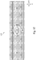
- FIGS. 9-12 illustrate top views of an air gap according to various embodiments of the present disclosure.
- FIGS. 13-15 illustrate cross-sectional side views of an air gap according to various embodiments of the present disclosure.
- FIG. 16 is a flowchart of a method for fabricating a FinFET device in accordance with embodiments of the present disclosure.
- first and second features are formed in direct contact
- additional features may be formed between the first and second features, such that the first and second features may not be in direct contact
- present disclosure may repeat reference numerals and/or letters in the various examples. This repetition is for the sake of simplicity and clarity and does not in itself dictate a relationship between the various embodiments and/or configurations discussed.
- various features may be arbitrarily drawn in different scales for the sake of simplicity and clarity.
- spatially relative terms such as “beneath,” “below,” “lower,” “above,” “upper” and the like, may be used herein for ease of description to describe one element or feature's relationship to another element(s) or feature(s) as illustrated in the figures.
- the spatially relative terms are intended to encompass different orientations of the device in use or operation in addition to the orientation depicted in the figures. For example, if the device in the figures is turned over, elements described as being “below” or “beneath” other elements or features would then be oriented “above” the other elements or features.
- the exemplary term “below” can encompass both an orientation of above and below.
- the apparatus may be otherwise oriented (rotated 90 degrees or at other orientations) and the spatially relative descriptors used herein may likewise be interpreted accordingly.
- the present disclosure is directed to, but not otherwise limited to, a fin-like field-effect transistor (FinFET) device.
- the FinFET device may be a complementary metal-oxide-semiconductor (CMOS) device including a P-type metal-oxide-semiconductor FinFET device and an N-type metal-oxide-semiconductor FinFET device.
- CMOS complementary metal-oxide-semiconductor
- the following disclosure will continue with one or more FinFET examples to illustrate various embodiments of the present disclosure. It is understood, however, that the application should not be limited to a particular type of device, except as specifically claimed.
- FIG. 1 a perspective view of an example FinFET device 50 is illustrated.
- the FinFET device 50 is a non-planar multi-gate transistor that is built over a substrate (such as a bulk substrate).
- a thin silicon-containing “fin-like” structure (hereinafter referred to as a “fin”) forms the body of the FinFET device 50 .
- the fin structure extends along an X-direction shown in FIG. 1 .
- the fin structure has a fin width W fin measured along a Y-direction that is orthogonal to the X-direction.
- a gate structure 60 of the FinFET device 50 partially wraps around this fin structure, for example around the top surface and the opposing sidewall surfaces of the fi structure n. Thus, a portion of the gate structure 60 is located over the fin structure in a Z-direction that is orthogonal to both the X-direction and the Y-direction.
- L G denotes a length (or width, depending on the perspective) of the gate structure 60 measured in the X-direction.
- the gate structure 60 may include a gate electrode component 60 A and a gate dielectric component 60 B.
- the gate dielectric 60 B has a thickness t ox measured in the Y-direction.
- a portion of the gate structure 60 is located over a dielectric isolation structure such as shallow trench isolation (STI).
- a source 70 and a drain 80 of the FinFET device 50 are formed in extensions of the fin structure on opposite sides of the gate structure 60 .
- a portion of the fin structure being wrapped around by the gate structure 60 serves as a channel of the FinFET device 50 .
- the effective channel length of the FinFET device 50 is determined by the dimensions of the fin structure.
- FinFET devices offer several advantages over traditional Metal-Oxide Semiconductor Field Effect Transistor (MOSFET) devices (also referred to as planar transistor devices). These advantages may include better chip area efficiency, improved carrier mobility, and fabrication processing that is compatible with the fabrication processing of planar devices. FinFET devices are also compatible with a high-k metal gate (HKMG) process flow. Thus, FinFET devices may be implemented as HKMG devices where the gates each that have a high-k gate dielectric and a metal gate electrode. For these benefits discussed above, it may be desirable to design an integrated circuit (IC) chip using FinFET devices for a portion of, or the entire IC chip.
- MOSFET Metal-Oxide Semiconductor Field Effect Transistor
- FinFET fabrication may include a gate-replacement process, where a dummy gate is replaced by the gate structure 60 , which may be a high-k metal gate.
- a “cut” may be made to the dummy gate to break up the dummy gate, so as to define individual dummy gates.
- the individual dummy gates are replaced by the high-k metal gates later.
- the “cut” defines the spacing or distance between the dummy gates in a direction in which the dummy gates extend.
- the “cut” may not sufficiently break up adjacent dummy gates. Undesirable residue of the dummy gates that remain (but should have been removed during the “cut”) may lead to leakage or line-end bridging issues between the eventually-formed high-k metal gates, which could adversely impact device performance and/or decrease yield.
- the present disclosure performs a “pull back” as a part of the “cut” process to enlarge the process window and reduce the possibility of line-end bridging.
- the resulting FinFET devices may contain voids or air gaps between adjacent gate structures. These voids or gaps may improve the electrical isolation between the adjacent gate structures.
- the FinFET devices fabricated herein may have improved device performance and yield compared to conventional FinFET devices.
- the fabrication process flow of the present disclosure is discussed below in more detail with reference to FIGS. 2A-8A, 2B-8B , and 9 - 16 .
- FIGS. 2A-8A are diagrammatic fragmentary top views of a FinFET device 100 at various stages of fabrication
- FIGS. 2B-8B are diagrammatic cross-sectional side views of the FinFET device 100 at various stages of fabrication.
- the cross-sectional views are obtained along the Y-cut shown in FIG. 1 , and the Y-cut is also illustrated in the top view of FIG. 2A .
- the FinFET device 100 includes a substrate 110 .
- the substrate 110 may be a semiconductor substrate, for example a silicon substrate in some embodiments.
- the substrate 110 may also include a doped well, which may be formed using one or more ion implantation processes that implant dopant ions into the substrate 110 .
- the dopant ions may include an n-type material in some embodiments, for example arsenic (As) or phosphorous (P), or they may include a p-type material in some other embodiments, for example boron (B), depending on whether an NFET or a PFET is needed.
- the FinFET device 100 includes fin structures 120 that protrude upwardly out of the substrate 110 , for example vertically upward in the Z-direction shown in FIG. 1 . Also while it is not immediately visible in FIG. 2B , the fin structures 120 are elongated structures and each extend in the X-direction, similar to the fin structure in FIG. 1 . Various portions of the fin structures 120 may serve as the source/drain regions or channel regions of FinFET transistors. Also as shown in FIG. 2B , the fin structures 120 are partially surrounded by (or embedded within) an isolation structure 150 . In some embodiments, the isolation structure 150 includes shallow trench isolation (STI). The isolation structure 150 provides electrical isolation between various components of the FinFET device 100 , for example the fin structures 120 .
- STI shallow trench isolation
- a dummy gate layer 160 is formed over the isolation structure 150 .
- the dummy gate layer 160 also is formed over, and partially wraps around, portions of the fin structures 120 .
- the dummy gate layer 160 includes polysilicon. The dummy gate layer 160 will be patterned into dummy gate structures subsequently and will be removed and replaced by high-k metal gates in a gate replacement process performed later.
- a patterned mask layer 170 is formed over the dummy gate layer 160 .
- the patterned mask layer 170 includes a dielectric material such as silicon oxynitride (SiON).
- the patterned mask layer 170 will serve as a hard mask in a patterning process discussed below.
- the patterned mask layer 170 includes an opening 175 .
- the opening 175 may be defined by forming a mask layer material and forming a patterned photoresist layer, and using the patterned photoresist layer to etch the opening into the mask layer material.
- the opening 175 will be extended further into the dummy gate layer 160 in a subsequent process discussed below.
- gate spacers 180 are formed on either sides of the dummy gate layer 160 , as shown in FIG. 2A .
- the gate spacers 180 are not directly visible in the cross-sectional view of FIG. 2B (or any of the cross-sectional view figures in the subsequent fabrication processing stages), since the cut-line Y-Y is taken at a location outside of the gate spacers 180 .
- the gate spacers 180 include a dielectric material, which may be different from the material of the patterned mask layer 170 .
- the gate spacers 180 may include silicon nitride (SiN), silicon oxynitride (SiON), silicon oxycarbonitride (SiOCN), silicon carbide (SiC), silicon oxycarbide (SiOC), or combinations thereof.
- the gate spacers 180 each have a lateral dimension 190 that is measured in the X-direction (e.g., the X-direction shown in FIG. 1 ). In some embodiments, the lateral dimension 190 is in a range between about 5 angstroms and about 500 angstroms.
- an etching process 200 is performed to the FinFET device 100 to further etch the opening 175 into the dummy gate layer 160 .
- the opening 175 of the patterned mask layer 170 becomes an opening (or recess) 20 that extends vertically through the dummy gate layer 160 in the Z-direction (e.g., the Z-direction shown in FIG. 1 ).
- the etching process 200 may also be referred to as a cut-poly etching process, since it “cuts open” the dummy gate layer 160 (which contains polysilicon in the illustrated embodiment.
- the dummy gate layer 160 is now separated into individual dummy gate structures 160 .
- the opening 210 has a dimension 230 that is measured in the Y-direction.
- the dimension 230 is one of the critical dimensions (CD) of the FinFET device 100 .
- the dimension 230 is in a range between about 3 nanometers (nm) and about 50 nm.
- the “pull back” process 250 is performed using: a power that is in a range between about 200 watts and about 1500 watts, a bias that is in a range between about 500 volts and about 2000 volts, a pressure that is in a range between about 3 milli-Torrs about 100 milli-Torrs, and a process time that is in a range between about 5 seconds and about 50 seconds.
- the opening 210 is widened into an opening 210 A, which now has a lateral dimension 260 that is measured in the Y-direction.
- the lateral dimension 260 is greater than the lateral dimension 230 shown in FIGS. 3A-3B .
- the lateral dimension 260 is in a range between about 5 nanometers and about 50 nm.
- the lateral dimension 260 may be configured by tuning the various parameters of the pull back process 250 .
- a polishing process 400 is performed to the FinFET device 100 to remove the patterned mask layer 170 and portions of the dielectric material 300 , as well as to planarize the upper surface of the FinFET device 100 .
- the polishing process 400 includes a chemical mechanical polishing (CMP) process. Some upper portions of the dummy gate structures 160 may also be removed by the polishing process 400 .
- the polishing process 400 may also remove a sufficient amount of the dielectric material 300 such that the air gap 310 is “opened up.” In other words, the air gap 310 is exposed as a result of the polishing process 400 being performed.
- the air gap 310 also does not have the high-k gate dielectric material and/or the metal gate electrode material formed within the air gap 310 .
- the air gap 310 shown in FIG. 12 may be oriented differently than the air gap 310 shown in FIG. 11 . For example, if the air gap 310 of FIG. 11 has a longer dimension measured in the Y-direction and a shorter dimension measured in the X-direction, then the air gap 310 of FIG. 12 has a shorter dimension measured in the Y-direction and a longer dimension measured in the X-direction, or vice versa.
Landscapes
- Engineering & Computer Science (AREA)
- Insulated Gate Type Field-Effect Transistor (AREA)
- Physics & Mathematics (AREA)
- Condensed Matter Physics & Semiconductors (AREA)
- General Physics & Mathematics (AREA)
- Manufacturing & Machinery (AREA)
- Computer Hardware Design (AREA)
- Microelectronics & Electronic Packaging (AREA)
- Power Engineering (AREA)
- Thin Film Transistor (AREA)
- Electrodes Of Semiconductors (AREA)
Abstract
Description
Claims (20)
Priority Applications (3)
| Application Number | Priority Date | Filing Date | Title |
|---|---|---|---|
| US16/203,987 US11043408B2 (en) | 2017-11-15 | 2018-11-29 | Method of forming FinFET devices with embedded air gaps |
| US17/349,741 US12057343B2 (en) | 2017-11-15 | 2021-06-16 | FinFET devices with embedded air gaps and the fabrication thereof |
| US18/771,846 US20240371682A1 (en) | 2017-11-15 | 2024-07-12 | Finfet devices with embedded air gaps and the fabrication thereof |
Applications Claiming Priority (3)
| Application Number | Priority Date | Filing Date | Title |
|---|---|---|---|
| US201762586223P | 2017-11-15 | 2017-11-15 | |
| US15/847,307 US10366915B2 (en) | 2017-11-15 | 2017-12-19 | FinFET devices with embedded air gaps and the fabrication thereof |
| US16/203,987 US11043408B2 (en) | 2017-11-15 | 2018-11-29 | Method of forming FinFET devices with embedded air gaps |
Related Parent Applications (1)
| Application Number | Title | Priority Date | Filing Date |
|---|---|---|---|
| US15/847,307 Division US10366915B2 (en) | 2017-11-15 | 2017-12-19 | FinFET devices with embedded air gaps and the fabrication thereof |
Related Child Applications (1)
| Application Number | Title | Priority Date | Filing Date |
|---|---|---|---|
| US17/349,741 Division US12057343B2 (en) | 2017-11-15 | 2021-06-16 | FinFET devices with embedded air gaps and the fabrication thereof |
Publications (2)
| Publication Number | Publication Date |
|---|---|
| US20190148215A1 US20190148215A1 (en) | 2019-05-16 |
| US11043408B2 true US11043408B2 (en) | 2021-06-22 |
Family
ID=66432391
Family Applications (4)
| Application Number | Title | Priority Date | Filing Date |
|---|---|---|---|
| US15/847,307 Active US10366915B2 (en) | 2017-11-15 | 2017-12-19 | FinFET devices with embedded air gaps and the fabrication thereof |
| US16/203,987 Active US11043408B2 (en) | 2017-11-15 | 2018-11-29 | Method of forming FinFET devices with embedded air gaps |
| US17/349,741 Active 2039-06-02 US12057343B2 (en) | 2017-11-15 | 2021-06-16 | FinFET devices with embedded air gaps and the fabrication thereof |
| US18/771,846 Pending US20240371682A1 (en) | 2017-11-15 | 2024-07-12 | Finfet devices with embedded air gaps and the fabrication thereof |
Family Applications Before (1)
| Application Number | Title | Priority Date | Filing Date |
|---|---|---|---|
| US15/847,307 Active US10366915B2 (en) | 2017-11-15 | 2017-12-19 | FinFET devices with embedded air gaps and the fabrication thereof |
Family Applications After (2)
| Application Number | Title | Priority Date | Filing Date |
|---|---|---|---|
| US17/349,741 Active 2039-06-02 US12057343B2 (en) | 2017-11-15 | 2021-06-16 | FinFET devices with embedded air gaps and the fabrication thereof |
| US18/771,846 Pending US20240371682A1 (en) | 2017-11-15 | 2024-07-12 | Finfet devices with embedded air gaps and the fabrication thereof |
Country Status (5)
| Country | Link |
|---|---|
| US (4) | US10366915B2 (en) |
| KR (1) | KR102096974B1 (en) |
| CN (2) | CN115985912A (en) |
| DE (1) | DE102018100297A1 (en) |
| TW (1) | TWI685900B (en) |
Cited By (2)
| Publication number | Priority date | Publication date | Assignee | Title |
|---|---|---|---|---|
| US12094941B2 (en) | 2021-09-14 | 2024-09-17 | Samsung Electronics Co., Ltd. | Semiconductor devices |
| US12476113B2 (en) * | 2015-10-30 | 2025-11-18 | Taiwan Semiconductor Manufacturing Company, Ltd. | Semiconductor device and manufacturing method thereof |
Families Citing this family (13)
| Publication number | Priority date | Publication date | Assignee | Title |
|---|---|---|---|---|
| US10366915B2 (en) | 2017-11-15 | 2019-07-30 | Taiwan Semiconductor Manufacturing Co., Ltd. | FinFET devices with embedded air gaps and the fabrication thereof |
| US11404536B2 (en) * | 2018-03-30 | 2022-08-02 | Intel Corporation | Thin-film transistor structures with gas spacer |
| KR102636464B1 (en) * | 2018-06-12 | 2024-02-14 | 삼성전자주식회사 | Semiconductor device having gate isolation layer and method of manufacturing the same |
| US12009266B2 (en) | 2019-12-18 | 2024-06-11 | Taiwan Semiconductor Manufacturing Co., Ltd. | Structure for fringing capacitance control |
| US11417750B2 (en) | 2020-01-31 | 2022-08-16 | Taiwan Semiconductor Manufacturing Co., Ltd. | Gate air spacer for fin-like field effect transistor |
| DE102020135077A1 (en) | 2020-01-31 | 2021-08-05 | Taiwan Semiconductor Manufacturing Co., Ltd. | GATE AIR SPACER FOR FIN-LIKE FIELD EFFECT TRANSISTORS |
| CN113394098B (en) * | 2020-03-13 | 2024-07-19 | 中芯国际集成电路制造(上海)有限公司 | Semiconductor structure and method of forming the same |
| US11164793B2 (en) * | 2020-03-23 | 2021-11-02 | International Business Machines Corporation | Reduced source/drain coupling for CFET |
| US11532479B2 (en) | 2020-04-01 | 2022-12-20 | Taiwan Semiconductor Manufacturing Company, Ltd. | Cut metal gate refill with void |
| CN113764278A (en) * | 2020-06-03 | 2021-12-07 | 中芯国际集成电路制造(上海)有限公司 | Method for forming semiconductor structure |
| US11842933B2 (en) * | 2021-01-15 | 2023-12-12 | Taiwan Semiconductor Manufacturing Co., Ltd. | Semiconductor device and method |
| US12087775B2 (en) * | 2021-07-08 | 2024-09-10 | Taiwan Semiconductor Manufacturing Co., Ltd. | Gate structures in transistor devices and methods of forming same |
| US20240014041A1 (en) * | 2022-07-05 | 2024-01-11 | Taiwan Semiconductor Manufacturing Company, Ltd. | Semiconductor device structure with gate stack and method for forming the same |
Citations (76)
| Publication number | Priority date | Publication date | Assignee | Title |
|---|---|---|---|---|
| US20080014760A1 (en) | 2006-07-12 | 2008-01-17 | Renesas Technology Corp. | Semiconductor device and method of manufacturing the same |
| US7425740B2 (en) | 2005-10-07 | 2008-09-16 | Taiwan Semiconductor Manufacturing Company, Ltd. | Method and structure for a 1T-RAM bit cell and macro |
| US20090302367A1 (en) | 2008-06-10 | 2009-12-10 | Kabushiki Kaisha Toshiba | Method of fabricating semiconductor device and semiconductor device fabricated by the method |
| US7667271B2 (en) | 2007-04-27 | 2010-02-23 | Taiwan Semiconductor Manufacturing Company, Ltd. | Fin field-effect transistors |
| US7910453B2 (en) | 2008-07-14 | 2011-03-22 | Taiwan Semiconductor Manufacturing Company, Ltd. | Storage nitride encapsulation for non-planar sonos NAND flash charge retention |
| US20110068407A1 (en) | 2009-09-24 | 2011-03-24 | Taiwan Semiconductor Manufacturing Company, Ltd. | Germanium FinFETs with Metal Gates and Stressors |
| US7915156B2 (en) | 2008-02-26 | 2011-03-29 | Kabushiki Kaisha Toshiba | Semiconductor memory device and method for manufacturing the same |
| US20110084340A1 (en) * | 2009-10-14 | 2011-04-14 | Feng Yuan | Voids in STI Regions for Forming Bulk FinFETs |
| US8048723B2 (en) | 2008-12-05 | 2011-11-01 | Taiwan Semiconductor Manufacturing Company, Ltd. | Germanium FinFETs having dielectric punch-through stoppers |
| US8053299B2 (en) | 2009-04-17 | 2011-11-08 | Taiwan Semiconductor Manufacturing Company, Ltd. | Method of fabrication of a FinFET element |
| US8183627B2 (en) | 2004-12-01 | 2012-05-22 | Taiwan Semiconductor Manufacturing Company, Ltd. | Hybrid fin field-effect transistor structures and related methods |
| US20120132982A1 (en) | 2010-11-29 | 2012-05-31 | Samsung Electronics Co., Ltd. | Non-Volatile Memory Devices |
| US20130011983A1 (en) | 2011-07-07 | 2013-01-10 | Taiwan Semiconductor Manufacturing Company, Ltd. | In-Situ Doping of Arsenic for Source and Drain Epitaxy |
| US8362575B2 (en) | 2009-09-29 | 2013-01-29 | Taiwan Semiconductor Manufacturing Company, Ltd. | Controlling the shape of source/drain regions in FinFETs |
| US8367498B2 (en) | 2010-10-18 | 2013-02-05 | Taiwan Semiconductor Manufacturing Company, Ltd. | Fin-like field effect transistor (FinFET) device and method of manufacturing same |
| US8377779B1 (en) | 2012-01-03 | 2013-02-19 | Taiwan Semiconductor Manufacturing Company, Ltd. | Methods of manufacturing semiconductor devices and transistors |
| US8399931B2 (en) | 2010-06-30 | 2013-03-19 | Taiwan Semiconductor Manufacturing Company, Ltd. | Layout for multiple-fin SRAM cell |
| US8415718B2 (en) | 2009-10-30 | 2013-04-09 | Taiwan Semiconductor Manufacturing Company, Ltd. | Method of forming epi film in substrate trench |
| US8440517B2 (en) | 2010-10-13 | 2013-05-14 | Taiwan Semiconductor Manufacturing Company, Ltd. | FinFET and method of fabricating the same |
| US8487378B2 (en) | 2011-01-21 | 2013-07-16 | Taiwan Semiconductor Manufacturing Company, Ltd. | Non-uniform channel junction-less transistor |
| US8497177B1 (en) | 2012-10-04 | 2013-07-30 | Taiwan Semiconductor Manufacturing Company, Ltd. | Method of making a FinFET device |
| US8497528B2 (en) | 2010-05-06 | 2013-07-30 | Taiwan Semiconductor Manufacturing Company, Ltd. | Method for fabricating a strained structure |
| US20130285153A1 (en) | 2012-04-25 | 2013-10-31 | Taiwan Semiconductor Manufacturing Company Ltd. | Strained structure of semiconductor device and method of making the strained structure |
| US8609518B2 (en) | 2011-07-22 | 2013-12-17 | Taiwan Semiconductor Manufacturing Company, Ltd. | Re-growing source/drain regions from un-relaxed silicon layer |
| US8610240B2 (en) | 2009-10-16 | 2013-12-17 | Taiwan Semiconductor Manufacturing Company, Ltd. | Integrated circuit with multi recessed shallow trench isolation |
| US8618556B2 (en) | 2011-06-30 | 2013-12-31 | Taiwan Semiconductor Manufacturing Company, Ltd. | FinFET design and method of fabricating same |
| US20140001574A1 (en) | 2011-09-08 | 2014-01-02 | Taiwan Semiconductor Manufacturing Company, Ltd. | Improved silicide formation and associated devices |
| US8633516B1 (en) | 2012-09-28 | 2014-01-21 | Taiwan Semiconductor Manufacturing Company, Ltd. | Source/drain stack stressor for semiconductor device |
| US8652894B2 (en) | 2010-02-11 | 2014-02-18 | Taiwan Semiconductor Manufacturing Company, Ltd. | Method for fabricating a FinFET device |
| US8680576B2 (en) | 2012-05-16 | 2014-03-25 | Taiwan Semiconductor Manufacturing Company, Ltd. | CMOS device and method of forming the same |
| US8703565B2 (en) | 2010-02-09 | 2014-04-22 | Taiwan Semiconductor Manufacturing Company, Ltd. | Bottom-notched SiGe FinFET formation using condensation |
| US20140110755A1 (en) | 2012-10-24 | 2014-04-24 | Taiwan Semiconductor Manufacturing Company, Ltd. | Apparatus and Method for Forming Semiconductor Contacts |
| US8716765B2 (en) | 2012-03-23 | 2014-05-06 | Taiwan Semiconductor Manufacturing Company, Ltd. | Contact structure of semiconductor device |
| US8723272B2 (en) | 2011-10-04 | 2014-05-13 | Taiwan Semiconductor Manufacturing Company, Ltd. | FinFET device and method of manufacturing same |
| US8729634B2 (en) | 2012-06-15 | 2014-05-20 | Taiwan Semiconductor Manufacturing Company, Ltd. | FinFET with high mobility and strain channel |
| US8729627B2 (en) | 2010-05-14 | 2014-05-20 | Taiwan Semiconductor Manufacturing Company, Ltd. | Strained channel integrated circuit devices |
| US8735993B2 (en) | 2012-01-31 | 2014-05-27 | Taiwan Semiconductor Manufacturing Company, Ltd. | FinFET body contact and method of making same |
| US8736056B2 (en) | 2012-07-31 | 2014-05-27 | Taiwan Semiconductor Manufacturing Company, Ltd. | Device for reducing contact resistance of a metal |
| US8742509B2 (en) | 2012-03-01 | 2014-06-03 | Taiwan Semiconductor Manufacturing Company, Ltd. | Apparatus and method for FinFETs |
| US20140151812A1 (en) | 2012-11-30 | 2014-06-05 | Taiwan Semiconductor Manufacturing Company, Ltd. | Contact Plugs in SRAM Cells and the Method of Forming the Same |
| US20140183600A1 (en) | 2012-12-28 | 2014-07-03 | Taiwan Semiconductor Manufacturing Company, Ltd. | Novel fin structure of finfet |
| US8776734B1 (en) | 2008-05-19 | 2014-07-15 | Innovative Environmental Solutions, Llc | Remedial system: a pollution control device for utilizing and abating volatile organic compounds |
| US8785285B2 (en) | 2012-03-08 | 2014-07-22 | Taiwan Semiconductor Manufacturing Company, Ltd. | Semiconductor devices and methods of manufacture thereof |
| US8796759B2 (en) | 2010-07-15 | 2014-08-05 | Taiwan Semiconductor Manufacturing Company, Ltd. | Fin-like field effect transistor (FinFET) device and method of manufacturing same |
| US8796666B1 (en) | 2013-04-26 | 2014-08-05 | Taiwan Semiconductor Manufacturing Company, Ltd. | MOS devices with strain buffer layer and methods of forming the same |
| US8809139B2 (en) | 2012-11-29 | 2014-08-19 | Taiwan Semiconductor Manufacturing Company, Ltd. | Fin-last FinFET and methods of forming same |
| US8815712B2 (en) | 2011-12-28 | 2014-08-26 | Taiwan Semiconductor Manufacturing Company, Ltd. | Method for epitaxial re-growth of semiconductor region |
| US8816444B2 (en) | 2011-04-29 | 2014-08-26 | Taiwan Semiconductor Manufacturing Company, Ltd. | System and methods for converting planar design to FinFET design |
| US8826213B1 (en) | 2013-03-11 | 2014-09-02 | Taiwan Semiconductor Manufacturing Company, Ltd. | Parasitic capacitance extraction for FinFETs |
| US8823065B2 (en) | 2012-11-08 | 2014-09-02 | Taiwan Semiconductor Manufacturing Company, Ltd. | Contact structure of semiconductor device |
| US8828823B2 (en) | 2011-10-13 | 2014-09-09 | Taiwan Semiconductor Manufacturing Company, Ltd. | FinFET device and method of manufacturing same |
| US20140252412A1 (en) | 2013-03-06 | 2014-09-11 | Taiwan Semiconductor Manufacturing Co., Ltd. | Strained and Uniform Doping Technique for FINFETs |
| US8836016B2 (en) | 2012-03-08 | 2014-09-16 | Taiwan Semiconductor Manufacturing Company, Ltd. | Semiconductor structures and methods with high mobility and high energy bandgap materials |
| US20140282326A1 (en) | 2013-03-12 | 2014-09-18 | Taiwan Semiconductor Manufacturing Company, Ltd. | Methods for Layout Verification for Polysilicon Cell Edge Structures in FinFET Standard Cells |
| US20140264590A1 (en) | 2013-03-13 | 2014-09-18 | Taiwan Semiconductor Manufacturing Company, Ltd. | FinFET with Bottom SiGe Layer in Source/Drain |
| US20140264592A1 (en) | 2013-03-12 | 2014-09-18 | Taiwan Semiconductor Manufacturing Co. Ltd. | Barrier Layer for FinFET Channels |
| US8841701B2 (en) | 2011-08-30 | 2014-09-23 | Taiwan Semiconductor Manufacturing Company, Ltd. | FinFET device having a channel defined in a diamond-like shape semiconductor structure |
| US8847293B2 (en) | 2012-03-02 | 2014-09-30 | Taiwan Semiconductor Manufacturing Company, Ltd. | Gate structure for semiconductor device |
| US8853025B2 (en) | 2013-02-08 | 2014-10-07 | Taiwan Semiconductor Manufacturing Company, Ltd. | FinFET/tri-gate channel doping for multiple threshold voltage tuning |
| US8860148B2 (en) | 2012-04-11 | 2014-10-14 | Taiwan Semiconductor Manufacturing Company, Ltd. | Structure and method for FinFET integrated with capacitor |
| US8887106B2 (en) | 2011-12-28 | 2014-11-11 | Taiwan Semiconductor Manufacturing Company, Ltd. | Method of generating a bias-adjusted layout design of a conductive feature and method of generating a simulation model of a predefined fabrication process |
| US9105490B2 (en) | 2012-09-27 | 2015-08-11 | Taiwan Semiconductor Manufacturing Company, Ltd. | Contact structure of semiconductor device |
| US20150263003A1 (en) | 2014-03-13 | 2015-09-17 | Taiwan Semiconductor Manufacturing Company, Ltd. | FinFET Devices with Unique Fin Shape and the Fabrication Thereof |
| US20150348966A1 (en) | 2014-05-30 | 2015-12-03 | Semiconductor Manufacturing International (Shanghai) Corporation | Fin field-effct transistors and fabrication method thereof |
| US20160049336A1 (en) | 2014-08-15 | 2016-02-18 | Samsung Electronics Co., Ltd. | Method for manufacturing semiconductor device |
| KR20160056693A (en) | 2014-11-12 | 2016-05-20 | 삼성전자주식회사 | Integrated circuit device and method of manufacturing the same |
| KR20160074859A (en) | 2014-12-18 | 2016-06-29 | 삼성전자주식회사 | Semiconductor device, methods of forming patterns for semiconductor device, and methods of manufacturing semiconductor devices |
| US9530890B1 (en) | 2015-11-02 | 2016-12-27 | International Business Machines Corporation | Parasitic capacitance reduction |
| US9577115B2 (en) | 2010-08-11 | 2017-02-21 | Samsung Electronics Co., Ltd. | Semiconductor devices having air gaps |
| KR20170062079A (en) | 2015-11-27 | 2017-06-07 | 삼성전자주식회사 | Semiconductor device and method for fabricating the same |
| US20170194195A1 (en) * | 2015-12-31 | 2017-07-06 | International Business Machines Corporation | Reactive ion etching assisted lift-off processes for fabricating thick metallization patterns with tight pitch |
| US20170229451A1 (en) | 2016-02-05 | 2017-08-10 | Taiwan Semiconductor Manufacturing Co., Ltd. | Fin field effect transistor and method for fabricating the same |
| US20170229452A1 (en) | 2016-02-05 | 2017-08-10 | Taiwan Semiconductor Manufacturing Co., Ltd. | Fin field effect transistor and method for fabricating the same |
| US9805983B1 (en) | 2016-08-19 | 2017-10-31 | International Business Machines Corporation | Multi-layer filled gate cut to prevent power rail shorting to gate structure |
| US20190148215A1 (en) | 2017-11-15 | 2019-05-16 | Taiwan Semiconductor Manufacturing Co., Ltd. | FinFET Devices with Embedded Air Gaps and the Fabrication Thereof |
| US10381262B2 (en) * | 2017-04-20 | 2019-08-13 | International Business Machines Corporation | Fabrication of vertical transport fin field effect transistors with a self-aligned separator and an isolation region with an air gap |
Family Cites Families (2)
| Publication number | Priority date | Publication date | Assignee | Title |
|---|---|---|---|---|
| US9619581B2 (en) | 2013-12-20 | 2017-04-11 | Microsoft Technology Licensing, Llc | Constructing queries for execution over multi-dimensional data structures |
| US9660022B2 (en) * | 2015-08-20 | 2017-05-23 | United Microelectronics Corp. | Semiconductive device with a single diffusion break and method of fabricating the same |
-
2017
- 2017-12-19 US US15/847,307 patent/US10366915B2/en active Active
-
2018
- 2018-01-09 DE DE102018100297.1A patent/DE102018100297A1/en active Granted
- 2018-03-23 KR KR1020180034011A patent/KR102096974B1/en active Active
- 2018-05-09 CN CN202310157746.2A patent/CN115985912A/en active Pending
- 2018-05-09 CN CN201810437451.XA patent/CN109786329A/en active Pending
- 2018-05-10 TW TW107115929A patent/TWI685900B/en active
- 2018-11-29 US US16/203,987 patent/US11043408B2/en active Active
-
2021
- 2021-06-16 US US17/349,741 patent/US12057343B2/en active Active
-
2024
- 2024-07-12 US US18/771,846 patent/US20240371682A1/en active Pending
Patent Citations (84)
| Publication number | Priority date | Publication date | Assignee | Title |
|---|---|---|---|---|
| US8183627B2 (en) | 2004-12-01 | 2012-05-22 | Taiwan Semiconductor Manufacturing Company, Ltd. | Hybrid fin field-effect transistor structures and related methods |
| US7425740B2 (en) | 2005-10-07 | 2008-09-16 | Taiwan Semiconductor Manufacturing Company, Ltd. | Method and structure for a 1T-RAM bit cell and macro |
| US20080014760A1 (en) | 2006-07-12 | 2008-01-17 | Renesas Technology Corp. | Semiconductor device and method of manufacturing the same |
| US7667271B2 (en) | 2007-04-27 | 2010-02-23 | Taiwan Semiconductor Manufacturing Company, Ltd. | Fin field-effect transistors |
| US7915156B2 (en) | 2008-02-26 | 2011-03-29 | Kabushiki Kaisha Toshiba | Semiconductor memory device and method for manufacturing the same |
| US8776734B1 (en) | 2008-05-19 | 2014-07-15 | Innovative Environmental Solutions, Llc | Remedial system: a pollution control device for utilizing and abating volatile organic compounds |
| US20090302367A1 (en) | 2008-06-10 | 2009-12-10 | Kabushiki Kaisha Toshiba | Method of fabricating semiconductor device and semiconductor device fabricated by the method |
| US7910453B2 (en) | 2008-07-14 | 2011-03-22 | Taiwan Semiconductor Manufacturing Company, Ltd. | Storage nitride encapsulation for non-planar sonos NAND flash charge retention |
| US8048723B2 (en) | 2008-12-05 | 2011-11-01 | Taiwan Semiconductor Manufacturing Company, Ltd. | Germanium FinFETs having dielectric punch-through stoppers |
| US8053299B2 (en) | 2009-04-17 | 2011-11-08 | Taiwan Semiconductor Manufacturing Company, Ltd. | Method of fabrication of a FinFET element |
| US20110068407A1 (en) | 2009-09-24 | 2011-03-24 | Taiwan Semiconductor Manufacturing Company, Ltd. | Germanium FinFETs with Metal Gates and Stressors |
| US8362575B2 (en) | 2009-09-29 | 2013-01-29 | Taiwan Semiconductor Manufacturing Company, Ltd. | Controlling the shape of source/drain regions in FinFETs |
| US20110084340A1 (en) * | 2009-10-14 | 2011-04-14 | Feng Yuan | Voids in STI Regions for Forming Bulk FinFETs |
| US8610240B2 (en) | 2009-10-16 | 2013-12-17 | Taiwan Semiconductor Manufacturing Company, Ltd. | Integrated circuit with multi recessed shallow trench isolation |
| US8415718B2 (en) | 2009-10-30 | 2013-04-09 | Taiwan Semiconductor Manufacturing Company, Ltd. | Method of forming epi film in substrate trench |
| US8703565B2 (en) | 2010-02-09 | 2014-04-22 | Taiwan Semiconductor Manufacturing Company, Ltd. | Bottom-notched SiGe FinFET formation using condensation |
| US8652894B2 (en) | 2010-02-11 | 2014-02-18 | Taiwan Semiconductor Manufacturing Company, Ltd. | Method for fabricating a FinFET device |
| US8497528B2 (en) | 2010-05-06 | 2013-07-30 | Taiwan Semiconductor Manufacturing Company, Ltd. | Method for fabricating a strained structure |
| US8729627B2 (en) | 2010-05-14 | 2014-05-20 | Taiwan Semiconductor Manufacturing Company, Ltd. | Strained channel integrated circuit devices |
| US8399931B2 (en) | 2010-06-30 | 2013-03-19 | Taiwan Semiconductor Manufacturing Company, Ltd. | Layout for multiple-fin SRAM cell |
| US8796759B2 (en) | 2010-07-15 | 2014-08-05 | Taiwan Semiconductor Manufacturing Company, Ltd. | Fin-like field effect transistor (FinFET) device and method of manufacturing same |
| US9577115B2 (en) | 2010-08-11 | 2017-02-21 | Samsung Electronics Co., Ltd. | Semiconductor devices having air gaps |
| US8440517B2 (en) | 2010-10-13 | 2013-05-14 | Taiwan Semiconductor Manufacturing Company, Ltd. | FinFET and method of fabricating the same |
| US8367498B2 (en) | 2010-10-18 | 2013-02-05 | Taiwan Semiconductor Manufacturing Company, Ltd. | Fin-like field effect transistor (FinFET) device and method of manufacturing same |
| US20120132982A1 (en) | 2010-11-29 | 2012-05-31 | Samsung Electronics Co., Ltd. | Non-Volatile Memory Devices |
| US8487378B2 (en) | 2011-01-21 | 2013-07-16 | Taiwan Semiconductor Manufacturing Company, Ltd. | Non-uniform channel junction-less transistor |
| US8816444B2 (en) | 2011-04-29 | 2014-08-26 | Taiwan Semiconductor Manufacturing Company, Ltd. | System and methods for converting planar design to FinFET design |
| US8618556B2 (en) | 2011-06-30 | 2013-12-31 | Taiwan Semiconductor Manufacturing Company, Ltd. | FinFET design and method of fabricating same |
| US20130011983A1 (en) | 2011-07-07 | 2013-01-10 | Taiwan Semiconductor Manufacturing Company, Ltd. | In-Situ Doping of Arsenic for Source and Drain Epitaxy |
| US8609518B2 (en) | 2011-07-22 | 2013-12-17 | Taiwan Semiconductor Manufacturing Company, Ltd. | Re-growing source/drain regions from un-relaxed silicon layer |
| US8841701B2 (en) | 2011-08-30 | 2014-09-23 | Taiwan Semiconductor Manufacturing Company, Ltd. | FinFET device having a channel defined in a diamond-like shape semiconductor structure |
| US8686516B2 (en) | 2011-09-08 | 2014-04-01 | Taiwan Semiconductor Manufacturing Company, Ltd. | Silicide formation and associated devices |
| US20140001574A1 (en) | 2011-09-08 | 2014-01-02 | Taiwan Semiconductor Manufacturing Company, Ltd. | Improved silicide formation and associated devices |
| US8723272B2 (en) | 2011-10-04 | 2014-05-13 | Taiwan Semiconductor Manufacturing Company, Ltd. | FinFET device and method of manufacturing same |
| US8828823B2 (en) | 2011-10-13 | 2014-09-09 | Taiwan Semiconductor Manufacturing Company, Ltd. | FinFET device and method of manufacturing same |
| US8815712B2 (en) | 2011-12-28 | 2014-08-26 | Taiwan Semiconductor Manufacturing Company, Ltd. | Method for epitaxial re-growth of semiconductor region |
| US8887106B2 (en) | 2011-12-28 | 2014-11-11 | Taiwan Semiconductor Manufacturing Company, Ltd. | Method of generating a bias-adjusted layout design of a conductive feature and method of generating a simulation model of a predefined fabrication process |
| US8377779B1 (en) | 2012-01-03 | 2013-02-19 | Taiwan Semiconductor Manufacturing Company, Ltd. | Methods of manufacturing semiconductor devices and transistors |
| US8735993B2 (en) | 2012-01-31 | 2014-05-27 | Taiwan Semiconductor Manufacturing Company, Ltd. | FinFET body contact and method of making same |
| US8742509B2 (en) | 2012-03-01 | 2014-06-03 | Taiwan Semiconductor Manufacturing Company, Ltd. | Apparatus and method for FinFETs |
| US8847293B2 (en) | 2012-03-02 | 2014-09-30 | Taiwan Semiconductor Manufacturing Company, Ltd. | Gate structure for semiconductor device |
| US8836016B2 (en) | 2012-03-08 | 2014-09-16 | Taiwan Semiconductor Manufacturing Company, Ltd. | Semiconductor structures and methods with high mobility and high energy bandgap materials |
| US8785285B2 (en) | 2012-03-08 | 2014-07-22 | Taiwan Semiconductor Manufacturing Company, Ltd. | Semiconductor devices and methods of manufacture thereof |
| US8716765B2 (en) | 2012-03-23 | 2014-05-06 | Taiwan Semiconductor Manufacturing Company, Ltd. | Contact structure of semiconductor device |
| US8860148B2 (en) | 2012-04-11 | 2014-10-14 | Taiwan Semiconductor Manufacturing Company, Ltd. | Structure and method for FinFET integrated with capacitor |
| US20130285153A1 (en) | 2012-04-25 | 2013-10-31 | Taiwan Semiconductor Manufacturing Company Ltd. | Strained structure of semiconductor device and method of making the strained structure |
| US8680576B2 (en) | 2012-05-16 | 2014-03-25 | Taiwan Semiconductor Manufacturing Company, Ltd. | CMOS device and method of forming the same |
| US8729634B2 (en) | 2012-06-15 | 2014-05-20 | Taiwan Semiconductor Manufacturing Company, Ltd. | FinFET with high mobility and strain channel |
| US8736056B2 (en) | 2012-07-31 | 2014-05-27 | Taiwan Semiconductor Manufacturing Company, Ltd. | Device for reducing contact resistance of a metal |
| US9105490B2 (en) | 2012-09-27 | 2015-08-11 | Taiwan Semiconductor Manufacturing Company, Ltd. | Contact structure of semiconductor device |
| US8633516B1 (en) | 2012-09-28 | 2014-01-21 | Taiwan Semiconductor Manufacturing Company, Ltd. | Source/drain stack stressor for semiconductor device |
| US8497177B1 (en) | 2012-10-04 | 2013-07-30 | Taiwan Semiconductor Manufacturing Company, Ltd. | Method of making a FinFET device |
| US20140110755A1 (en) | 2012-10-24 | 2014-04-24 | Taiwan Semiconductor Manufacturing Company, Ltd. | Apparatus and Method for Forming Semiconductor Contacts |
| US8772109B2 (en) | 2012-10-24 | 2014-07-08 | Taiwan Semiconductor Manufacturing Company, Ltd. | Apparatus and method for forming semiconductor contacts |
| US8823065B2 (en) | 2012-11-08 | 2014-09-02 | Taiwan Semiconductor Manufacturing Company, Ltd. | Contact structure of semiconductor device |
| US8809139B2 (en) | 2012-11-29 | 2014-08-19 | Taiwan Semiconductor Manufacturing Company, Ltd. | Fin-last FinFET and methods of forming same |
| US20140151812A1 (en) | 2012-11-30 | 2014-06-05 | Taiwan Semiconductor Manufacturing Company, Ltd. | Contact Plugs in SRAM Cells and the Method of Forming the Same |
| US20140183600A1 (en) | 2012-12-28 | 2014-07-03 | Taiwan Semiconductor Manufacturing Company, Ltd. | Novel fin structure of finfet |
| US8853025B2 (en) | 2013-02-08 | 2014-10-07 | Taiwan Semiconductor Manufacturing Company, Ltd. | FinFET/tri-gate channel doping for multiple threshold voltage tuning |
| US20140252412A1 (en) | 2013-03-06 | 2014-09-11 | Taiwan Semiconductor Manufacturing Co., Ltd. | Strained and Uniform Doping Technique for FINFETs |
| US8826213B1 (en) | 2013-03-11 | 2014-09-02 | Taiwan Semiconductor Manufacturing Company, Ltd. | Parasitic capacitance extraction for FinFETs |
| US20140282326A1 (en) | 2013-03-12 | 2014-09-18 | Taiwan Semiconductor Manufacturing Company, Ltd. | Methods for Layout Verification for Polysilicon Cell Edge Structures in FinFET Standard Cells |
| US20140264592A1 (en) | 2013-03-12 | 2014-09-18 | Taiwan Semiconductor Manufacturing Co. Ltd. | Barrier Layer for FinFET Channels |
| US20140264590A1 (en) | 2013-03-13 | 2014-09-18 | Taiwan Semiconductor Manufacturing Company, Ltd. | FinFET with Bottom SiGe Layer in Source/Drain |
| US8796666B1 (en) | 2013-04-26 | 2014-08-05 | Taiwan Semiconductor Manufacturing Company, Ltd. | MOS devices with strain buffer layer and methods of forming the same |
| US20150263003A1 (en) | 2014-03-13 | 2015-09-17 | Taiwan Semiconductor Manufacturing Company, Ltd. | FinFET Devices with Unique Fin Shape and the Fabrication Thereof |
| US20150348966A1 (en) | 2014-05-30 | 2015-12-03 | Semiconductor Manufacturing International (Shanghai) Corporation | Fin field-effct transistors and fabrication method thereof |
| US20160260801A1 (en) | 2014-05-30 | 2016-09-08 | Semiconductor Manufacturing International (Shanghai) Corporation | Fin field-effct transistors |
| US20160049336A1 (en) | 2014-08-15 | 2016-02-18 | Samsung Electronics Co., Ltd. | Method for manufacturing semiconductor device |
| US9508727B2 (en) | 2014-11-12 | 2016-11-29 | Samsung Electronics Co., Ltd. | Integrated circuit device and method of manufacturing the same |
| KR20160056693A (en) | 2014-11-12 | 2016-05-20 | 삼성전자주식회사 | Integrated circuit device and method of manufacturing the same |
| US9741854B2 (en) | 2014-12-18 | 2017-08-22 | Samsung Electronics Co., Ltd. | Method for manufacturing semiconductor device |
| KR20160074859A (en) | 2014-12-18 | 2016-06-29 | 삼성전자주식회사 | Semiconductor device, methods of forming patterns for semiconductor device, and methods of manufacturing semiconductor devices |
| US9530890B1 (en) | 2015-11-02 | 2016-12-27 | International Business Machines Corporation | Parasitic capacitance reduction |
| KR20170062079A (en) | 2015-11-27 | 2017-06-07 | 삼성전자주식회사 | Semiconductor device and method for fabricating the same |
| US20170194195A1 (en) * | 2015-12-31 | 2017-07-06 | International Business Machines Corporation | Reactive ion etching assisted lift-off processes for fabricating thick metallization patterns with tight pitch |
| US20170229451A1 (en) | 2016-02-05 | 2017-08-10 | Taiwan Semiconductor Manufacturing Co., Ltd. | Fin field effect transistor and method for fabricating the same |
| CN107046031A (en) | 2016-02-05 | 2017-08-15 | 台湾积体电路制造股份有限公司 | Fin type field effect transistor |
| TW201729264A (en) | 2016-02-05 | 2017-08-16 | 台灣積體電路製造股份有限公司 | Fin type field effect transistor |
| TW201729265A (en) | 2016-02-05 | 2017-08-16 | 台灣積體電路製造股份有限公司 | Fin type field effect transistor |
| US20170229452A1 (en) | 2016-02-05 | 2017-08-10 | Taiwan Semiconductor Manufacturing Co., Ltd. | Fin field effect transistor and method for fabricating the same |
| US9805983B1 (en) | 2016-08-19 | 2017-10-31 | International Business Machines Corporation | Multi-layer filled gate cut to prevent power rail shorting to gate structure |
| US10381262B2 (en) * | 2017-04-20 | 2019-08-13 | International Business Machines Corporation | Fabrication of vertical transport fin field effect transistors with a self-aligned separator and an isolation region with an air gap |
| US20190148215A1 (en) | 2017-11-15 | 2019-05-16 | Taiwan Semiconductor Manufacturing Co., Ltd. | FinFET Devices with Embedded Air Gaps and the Fabrication Thereof |
Cited By (2)
| Publication number | Priority date | Publication date | Assignee | Title |
|---|---|---|---|---|
| US12476113B2 (en) * | 2015-10-30 | 2025-11-18 | Taiwan Semiconductor Manufacturing Company, Ltd. | Semiconductor device and manufacturing method thereof |
| US12094941B2 (en) | 2021-09-14 | 2024-09-17 | Samsung Electronics Co., Ltd. | Semiconductor devices |
Also Published As
| Publication number | Publication date |
|---|---|
| US12057343B2 (en) | 2024-08-06 |
| US20240371682A1 (en) | 2024-11-07 |
| KR20190055687A (en) | 2019-05-23 |
| DE102018100297A1 (en) | 2019-05-16 |
| US10366915B2 (en) | 2019-07-30 |
| TWI685900B (en) | 2020-02-21 |
| CN109786329A (en) | 2019-05-21 |
| KR102096974B1 (en) | 2020-04-06 |
| US20190148215A1 (en) | 2019-05-16 |
| TW201923906A (en) | 2019-06-16 |
| CN115985912A (en) | 2023-04-18 |
| US20210313216A1 (en) | 2021-10-07 |
| US20190148214A1 (en) | 2019-05-16 |
Similar Documents
| Publication | Publication Date | Title |
|---|---|---|
| US12057343B2 (en) | FinFET devices with embedded air gaps and the fabrication thereof | |
| US11728402B2 (en) | Structure and method for semiconductor devices | |
| US11699758B2 (en) | Isolation structure having different distances to adjacent FinFET devices | |
| US11043577B2 (en) | Semiconductor device and method of manufacturing the same | |
| KR20190002301A (en) | Metal gate structure cutting process | |
| US12237418B2 (en) | Liner for a bi-layer gate helmet and the fabrication thereof | |
| US11004846B2 (en) | Enlarging spacer thickness by forming a dielectric layer over a recessed interlayer dielectric | |
| US20240194764A1 (en) | Multi-gate devices with multi-layer inner spacers and fabrication methods thereof | |
| US12191379B2 (en) | Multi-gate semiconductor device with inner spacer and fabrication method thereof | |
| US11776961B2 (en) | Semiconductor device and manufacturing method thereof for selectively etching dummy fins | |
| CN108231683B (en) | Semiconductor device and method for manufacturing the same | |
| US20220320321A1 (en) | Method of manufacturing a semiconductor device and a semiconductor device | |
| US20240379859A1 (en) | Device Structure with Reduced Leakage Current | |
| US11557660B2 (en) | Method and device for forming cut-metal-gate feature | |
| US11908919B2 (en) | Multi-gate devices with multi-layer inner spacers and fabrication methods thereof |
Legal Events
| Date | Code | Title | Description |
|---|---|---|---|
| AS | Assignment |
Owner name: TAIWAN SEMICONDUCTOR MANUFACTURING CO., LTD., TAIW Free format text: ASSIGNMENT OF ASSIGNORS INTEREST;ASSIGNORS:CHANG, CHE-CHENG;LIN, CHIH-HAN;REEL/FRAME:047622/0635 Effective date: 20171123 Owner name: TAIWAN SEMICONDUCTOR MANUFACTURING CO., LTD., TAIWAN Free format text: ASSIGNMENT OF ASSIGNORS INTEREST;ASSIGNORS:CHANG, CHE-CHENG;LIN, CHIH-HAN;REEL/FRAME:047622/0635 Effective date: 20171123 |
|
| FEPP | Fee payment procedure |
Free format text: ENTITY STATUS SET TO UNDISCOUNTED (ORIGINAL EVENT CODE: BIG.); ENTITY STATUS OF PATENT OWNER: LARGE ENTITY |
|
| STPP | Information on status: patent application and granting procedure in general |
Free format text: APPLICATION DISPATCHED FROM PREEXAM, NOT YET DOCKETED |
|
| STPP | Information on status: patent application and granting procedure in general |
Free format text: DOCKETED NEW CASE - READY FOR EXAMINATION |
|
| STPP | Information on status: patent application and granting procedure in general |
Free format text: NON FINAL ACTION MAILED |
|
| STPP | Information on status: patent application and granting procedure in general |
Free format text: RESPONSE TO NON-FINAL OFFICE ACTION ENTERED AND FORWARDED TO EXAMINER |
|
| STPP | Information on status: patent application and granting procedure in general |
Free format text: FINAL REJECTION MAILED |
|
| STPP | Information on status: patent application and granting procedure in general |
Free format text: RESPONSE AFTER FINAL ACTION FORWARDED TO EXAMINER |
|
| STPP | Information on status: patent application and granting procedure in general |
Free format text: DOCKETED NEW CASE - READY FOR EXAMINATION |
|
| STPP | Information on status: patent application and granting procedure in general |
Free format text: NON FINAL ACTION MAILED |
|
| STPP | Information on status: patent application and granting procedure in general |
Free format text: RESPONSE TO NON-FINAL OFFICE ACTION ENTERED AND FORWARDED TO EXAMINER |
|
| STPP | Information on status: patent application and granting procedure in general |
Free format text: NOTICE OF ALLOWANCE MAILED -- APPLICATION RECEIVED IN OFFICE OF PUBLICATIONS |
|
| STPP | Information on status: patent application and granting procedure in general |
Free format text: PUBLICATIONS -- ISSUE FEE PAYMENT RECEIVED |
|
| STPP | Information on status: patent application and granting procedure in general |
Free format text: PUBLICATIONS -- ISSUE FEE PAYMENT VERIFIED |
|
| STCF | Information on status: patent grant |
Free format text: PATENTED CASE |
|
| MAFP | Maintenance fee payment |
Free format text: PAYMENT OF MAINTENANCE FEE, 4TH YEAR, LARGE ENTITY (ORIGINAL EVENT CODE: M1551); ENTITY STATUS OF PATENT OWNER: LARGE ENTITY Year of fee payment: 4 |