US11043273B2 - Vertical memory device and an operating method thereof - Google Patents
Vertical memory device and an operating method thereof Download PDFInfo
- Publication number
- US11043273B2 US11043273B2 US16/581,917 US201916581917A US11043273B2 US 11043273 B2 US11043273 B2 US 11043273B2 US 201916581917 A US201916581917 A US 201916581917A US 11043273 B2 US11043273 B2 US 11043273B2
- Authority
- US
- United States
- Prior art keywords
- voltage
- dummy
- line
- string
- program
- Prior art date
- Legal status (The legal status is an assumption and is not a legal conclusion. Google has not performed a legal analysis and makes no representation as to the accuracy of the status listed.)
- Active
Links
Images


Classifications
-
- G—PHYSICS
- G11—INFORMATION STORAGE
- G11C—STATIC STORES
- G11C16/00—Erasable programmable read-only memories
- G11C16/02—Erasable programmable read-only memories electrically programmable
- G11C16/06—Auxiliary circuits, e.g. for writing into memory
- G11C16/10—Programming or data input circuits
- G11C16/14—Circuits for erasing electrically, e.g. erase voltage switching circuits
- G11C16/16—Circuits for erasing electrically, e.g. erase voltage switching circuits for erasing blocks, e.g. arrays, words, groups
-
- G—PHYSICS
- G11—INFORMATION STORAGE
- G11C—STATIC STORES
- G11C11/00—Digital stores characterised by the use of particular electric or magnetic storage elements; Storage elements therefor
- G11C11/56—Digital stores characterised by the use of particular electric or magnetic storage elements; Storage elements therefor using storage elements with more than two stable states represented by steps, e.g. of voltage, current, phase, frequency
- G11C11/5621—Digital stores characterised by the use of particular electric or magnetic storage elements; Storage elements therefor using storage elements with more than two stable states represented by steps, e.g. of voltage, current, phase, frequency using charge storage in a floating gate
- G11C11/5628—Programming or writing circuits; Data input circuits
- G11C11/5635—Erasing circuits
-
- G—PHYSICS
- G11—INFORMATION STORAGE
- G11C—STATIC STORES
- G11C16/00—Erasable programmable read-only memories
- G11C16/02—Erasable programmable read-only memories electrically programmable
- G11C16/04—Erasable programmable read-only memories electrically programmable using variable threshold transistors, e.g. FAMOS
- G11C16/0483—Erasable programmable read-only memories electrically programmable using variable threshold transistors, e.g. FAMOS comprising cells having several storage transistors connected in series
-
- G—PHYSICS
- G11—INFORMATION STORAGE
- G11C—STATIC STORES
- G11C16/00—Erasable programmable read-only memories
- G11C16/02—Erasable programmable read-only memories electrically programmable
- G11C16/06—Auxiliary circuits, e.g. for writing into memory
- G11C16/08—Address circuits; Decoders; Word-line control circuits
-
- G—PHYSICS
- G11—INFORMATION STORAGE
- G11C—STATIC STORES
- G11C16/00—Erasable programmable read-only memories
- G11C16/02—Erasable programmable read-only memories electrically programmable
- G11C16/06—Auxiliary circuits, e.g. for writing into memory
- G11C16/10—Programming or data input circuits
- G11C16/14—Circuits for erasing electrically, e.g. erase voltage switching circuits
-
- G—PHYSICS
- G11—INFORMATION STORAGE
- G11C—STATIC STORES
- G11C16/00—Erasable programmable read-only memories
- G11C16/02—Erasable programmable read-only memories electrically programmable
- G11C16/06—Auxiliary circuits, e.g. for writing into memory
- G11C16/24—Bit-line control circuits
-
- G—PHYSICS
- G11—INFORMATION STORAGE
- G11C—STATIC STORES
- G11C16/00—Erasable programmable read-only memories
- G11C16/02—Erasable programmable read-only memories electrically programmable
- G11C16/06—Auxiliary circuits, e.g. for writing into memory
- G11C16/32—Timing circuits
-
- G—PHYSICS
- G11—INFORMATION STORAGE
- G11C—STATIC STORES
- G11C16/00—Erasable programmable read-only memories
- G11C16/02—Erasable programmable read-only memories electrically programmable
- G11C16/06—Auxiliary circuits, e.g. for writing into memory
- G11C16/34—Determination of programming status, e.g. threshold voltage, overprogramming or underprogramming, retention
- G11C16/3436—Arrangements for verifying correct programming or erasure
- G11C16/344—Arrangements for verifying correct erasure or for detecting overerased cells
- G11C16/3445—Circuits or methods to verify correct erasure of nonvolatile memory cells
Definitions
- the inventive concept relates to a vertical memory device and an operating method thereof.
- an operating method of a memory device including a plurality of strings on a substrate, wherein the plurality of strings include a main string connected to a bit line and a dummy string spaced apart from the bit line, the operating method including: pre-programming the dummy string; and erasing the main string and the dummy string, wherein the pre-programming includes: applying a pre-program voltage to a word line connected to the dummy string; applying a pass voltage to a ground selection line connected to a ground selection transistor of the dummy string; and applying a common source line voltage to a common source line connected to the dummy string.
- a memory device including: a memory cell array including a plurality of strings each including memory cells respectively connected to word lines vertically stacked on a substrate; and a control logic configured to sequentially perform a pre-program operation and an erasing operation on the plurality of strings, wherein the plurality of strings include a main string to which a bit line is connected and a dummy string spaced apart from the bit line, and the control logic, to perform the pre-program operation, applies a pre-program voltage to at least one of the word lines connected to the dummy string, applies a pass voltage to a ground selection line connected to a ground selection transistor of the dummy string, and applies a common source line voltage to a common source line connected to the dummy string.
- a memory device including: a memory cell array including a plurality of strings each including memory cells respectively connected to word lines vertically stacked on a substrate; and a control logic configured to perform a pre-program operation on the plurality of strings, wherein the plurality of strings include a main string to which a bit line is connected and a dummy string spaced apart from the bit line, the control logic, during a pre-program operation, applies a pre-program voltage to the word lines, applies a pass voltage to a ground selection line connected to a ground selection transistor of the dummy string, and applies a first common source line voltage to a common source line connected to the dummy string, and a time in which the pre-program voltage is applied to the word lines, a time in which the pass voltage is applied to the ground selection line, and a time in which the first common source line voltage is applied to the common source line overlap one another.
- an operating method of a memory device including a plurality of strings, wherein the plurality of strings include a first string connected to a first bit line of a plurality of bit lines and a second string not connected to the bit lines, the operating method including: applying a pre-program voltage to a word line connected to the second string; applying a pass voltage to a ground selection line connected to a ground selection transistor of the second string; and applying a common source line voltage to a common source line connected to the second string.
- FIG. 1 is a block diagram illustrating a memory device according to an exemplary embodiment of the inventive concept
- FIGS. 2A, 2B and 2C are views for explaining a first memory block illustrated in FIG. 1 , according to an exemplary embodiment of the inventive concept;
- FIG. 3A is a flowchart illustrating an operating method of a memory device, according to an exemplary embodiment of the inventive concept
- FIG. 3B is a table illustrating voltage conditions during a pre-program operation performed by a memory device according to an exemplary embodiment of the inventive concept
- FIGS. 4, 5, 6, 7 and 8 are timing diagrams of voltages applied to each line during a pre-program operation and an erasing operation performed by a memory device according to an exemplary embodiment of the inventive concept;
- FIG. 9 is a cross-sectional view illustrating memory blocks included in a memory device according to an exemplary embodiment of the inventive concept.
- FIGS. 10A, 10B and 10C are tables illustrating voltage conditions applied to word lines and dummy word lines when a memory device according to an exemplary embodiment of the inventive concept performs a pre-program operation
- FIGS. 11A and 11B are views for explaining the first memory block illustrated in FIG. 1 , according to an exemplary embodiment of the inventive concept;
- FIGS. 12A and 12B are tables illustrating voltage conditions applied to bit lines and dummy bit lines when a memory device according to an exemplary embodiment of the inventive concept performs a pre-program operation
- FIG. 13 is a block diagram illustrating a case in which a memory device according to exemplary embodiments of the inventive concept is applied to a solid state drive (SSD) system.
- SSD solid state drive
- FIG. 1 is a block diagram illustrating a memory device 100 according to an exemplary embodiment of the inventive concept.
- the memory device 100 may include a memory cell array 110 , a control logic 120 , a voltage generator 130 , a row decoder 140 , and a page buffer 150 .
- the memory device 100 may further include various other components related to memory operations.
- the memory device 100 may include a data input/output circuit and an input/output interface.
- the memory cell array 110 includes a plurality of memory cells and may be connected to word lines WL, string selection lines SSL, ground selection lines GSL, common source lines, and bit lines BL.
- the memory cell array 110 may be connected to the row decoder 140 via the word lines WL, the string selection lines SSL, and the ground selection lines GSL, and may be connected to the page buffer 150 via the bit lines BL.
- the plurality of memory cells included in the memory cell array 110 may be non-volatile memory cells that retain stored data even when their power supply is interrupted.
- the memory device 100 may be an electrically erasable programmable read-only memory (EEPROM), a flash memory, a phase change random access memory (PRAM), a resistance random access memory (RRAM), a nano floating gate memory (NFGM), a polymer random access memory (PoRAM), a magnetic random access memory (MRAM), a ferroelectric random access memory (FRAM), or the like.
- EEPROM electrically erasable programmable read-only memory
- PRAM phase change random access memory
- RRAM resistance random access memory
- NFGM nano floating gate memory
- PoRAM polymer random access memory
- MRAM magnetic random access memory
- FRAM ferroelectric random access memory
- the memory cell array 110 may include a plurality of memory blocks BLK 1 to BLKz.
- each of the memory blocks BLK 1 to BLKz may have a three-dimensional structure (or vertical structure).
- each of the memory blocks BLK 1 to BLKz may include structures extending in first, second and third directions.
- each of the memory blocks BLK 1 to BLKz may include a plurality of NAND strings (hereinafter, referred to as ‘strings’) extending in the third direction.
- a plurality of strings may be spaced apart by certain distances in the first and second directions.
- a plurality of strings may include a cell string including main cells in which data is stored and a dummy string including dummy cells.
- the memory blocks BLK 1 to BLKz may be selected by the row decoder 140 .
- the row decoder 140 may select a memory block corresponding to a block address from among the memory blocks BLK 1 to BLKz.
- an erasing operation may be performed, and a pre-program operation corresponding to the erasing operation may be performed.
- the inventive concept is not limited thereto.
- an erasing operation may be performed and a pre-program operation corresponding to the erasing operation may be performed.
- Each memory cell included in the memory cell array 110 may be a multi level cell (MLC) that stores two or more bits of data.
- the memory cell may be an MLC that stores 2-bit data.
- the memory cell may be a triple level cell (TLC) that stores 3-bit data.
- TLC triple level cell
- some memory cells included in the memory cell array 110 may be single level cells (SLCs) that store 1-bit data and other memory cells included the memory cell array 110 may be MLCs.
- the memory blocks BLK 1 to BLKz may include a SLC block including SLCs, a MLC block including MLCs, or a TLC block including TLCs. From among a plurality of memory blocks included in the memory cell array 110 , some memory blocks may be SLC blocks and other memory blocks may be MLC blocks or TLC blocks.
- a plurality of memory cells When an erasing voltage is applied to the memory cell array 110 , a plurality of memory cells may be in an erased state.
- a program voltage When a program voltage is applied to the memory cell array 110 , a plurality of memory cells may be in a program state.
- a pre-program voltage When a pre-program voltage is applied to the memory cell array 110 , a plurality of memory cells may be in a pre-programmed state.
- each memory cell may have an erased state E and at least one program state, which are identified according to a threshold voltage (V th ).
- the control logic 120 may output various control signals for programming data into the memory cell array 110 or reading data from the memory cell array 110 , based on a command CMD, an address ADDR, and a control signal CTRL transmitted by a memory controller. For example, the control logic 120 may output a voltage control signal CTRL_vol for controlling the level of various voltages generated by the voltage generator 130 .
- the control logic 120 may provide a row address X-ADDR to the row decoder 140 and a column address Y-ADDR to the page buffer 150 .
- the voltage generator 130 may generate various voltages used in the memory device 100 and may generate, for example, a word line voltage VWL, a string selection line voltage VSSL, and a ground selection line voltage VGSL.
- the voltage generator 130 may generate a common source line voltage and a substrate voltage that is to be applied to a substrate on which the memory cell array 110 is formed.
- the word line voltage VWL may include a pre-program voltage (for example, Vprepro illustrated in FIG. 3B ) and the ground selection line voltage VGSL may include a pass voltage (e.g., Vpass illustrated in FIG. 3B ).
- the row decoder 140 may select at least one of the word lines of the selected memory block in response to the row address X-ADDR.
- the row decoder 140 may, in response to the row address X-ADDR, apply a pre-program voltage Vprepro as a word line voltage VWL to at least one word line of the word lines WL.
- the row decoder 140 may apply a pass voltage Vpass as a ground selection line voltage VGSL to at least one of the ground selection lines GSL.
- the memory cell array 110 may be connected to a dummy word line and the row decoder 140 may, during a pre-program operation, selectively apply a pre-program voltage Vprepro to the dummy word line.
- the row decoder 140 may provide the pre-program voltage Vprepro as a word line voltage VWL to the word line (e.g., the dummy word line) of the selected memory cell in response to the row address X-ADDR, and may provide the word line pass voltage as a word line voltage VWL to the word line of the unselected memory cell.
- the magnitude of the pre-program voltage Vprepro may differ from the magnitude of the program voltage applied to word lines WL to write data to the memory cells.
- the pre-program voltage Vprepro may have a level lower than the program voltage.
- the memory device 100 may apply a plurality of program pulses to word lines WL during a program operation to write data to the memory cells and may apply a pre-program voltage Vprepro having a single pulse to word lines WL during a pre-program operation.
- the page buffer 150 may operate as a write driver or a sense amplifier. In an exemplary embodiment of the inventive concept, during a pre-program operation, the page buffer 150 acts as a write driver and applies a bit line program voltage to at least one bit line of bit lines BL.
- the control logic 120 may control the voltage generator 130 and the row decoder 140 to perform a pre-program operation and an erasing operation. For example, when a pre-program operation is performed with respect to a dummy string, the control logic 120 may control the voltage generator 130 and the row decoder 140 to apply a pass voltage Vpass to a ground selection line connected to the dummy string. In an exemplary embodiment of the inventive concept, the control logic 120 may control a ground voltage to be applied to a common source line connected to a memory block in which a pre-program operation is performed.
- the memory device 100 may perform a pre-program operation on a dummy string by applying a ground voltage to a common source line, a pass voltage Vpass to a ground selection line, and a pre-program voltage Vprepro to a word line.
- the memory device 100 may pre-program the dummy cells in the dummy string even when the dummy string is not connected to the bit line.
- the threshold voltage distribution of the dummy cells included in the dummy string may be shifted in a direction in which the threshold voltage is increased.
- the pre-program operation with respect to the dummy string is performed before or after the erasing operation, thereby preventing the dummy cells included in the dummy string from being damaged due to the repeated erasing operation.
- FIGS. 2A to 2C are views for explaining a first memory block illustrated in FIG. 1 , according to an exemplary embodiment of the inventive concept.
- FIG. 2A is a top view of the first memory block illustrated in FIG. 1 .
- FIG. 2B illustrates a cross-section taken along the line A-A′ illustrated in FIG. 2A .
- FIG. 2C is a circuit diagram showing an equivalent circuit of region B of the memory block of FIG. 2A .
- the memory block BLK 1 may be a vertical NAND flash memory, and each of the memory blocks BLK 1 to BLKz illustrated in FIG. 1 may be implemented as shown in FIGS. 2A to 2C .
- the memory block BLK 1 may include word line cut regions WLC that are spaced apart from each other in a first direction X and that extend in a second direction Y.
- the memory block BLK 1 may include a plurality of vertical holes (for example, main holes H 11 , H 31 , H 61 , and H 81 and a dummy hole DH 1 in FIG. 2B ) arranged in the first and second directions Y between the word line cut regions WLC.
- the vertical holes may include main holes (for example, H 11 , H 31 , H 61 , and H 81 in FIG.
- the dummy holes DI are shown as being arranged in the central region of the memory block BLK 1 , but the inventive concept is not limited thereto, and the arrangement of the dummy holes DH may vary.
- the dummy holes DH may be arranged to the left or the right of the central region of the memory block BLK 1 .
- the memory block BLK 1 may be connected to bit lines BL 1 , BL 2 , BL 3 , BL 4 , BL 5 , BL 6 , BL 7 and BL 8 extending in the second direction Y and spaced apart from each other in the first direction X.
- the memory block BLK 1 is connected to eight bit lines, for example, the bit lines BL 1 to BL 8 .
- the inventive concept is not limited thereto, and the number of bit lines may vary.
- the main holes may be respectively connected to corresponding bit lines, and the dummy holes DH may be electrically spaced away from the bit lines BL 1 to BL 8 .
- the vertical holes connected to the first bit line BL are main holes, and main cells formed in the main holes may perform a data storage function.
- the dummy holes DH are vertical holes that are not connected to the bit lines BL 1 to BL 8 , and memory cells formed in the dummy holes DH, in other words, dummy cells, may not perform the data storage function.
- a ground selection line GSL, a plurality of word lines WL 1 , WL 2 , WL 3 , WL 4 , WL 5 , WL 6 , WL 7 and WL 8 , and a string selection line SSL may be arranged on a substrate SUB.
- Insulating films IL may be sequentially provided among the substrate SUB, the ground selection line GSL, the word lines WL 1 to WL 8 , and the string selection line SSL.
- the main holes H 11 , H 31 , H 61 , and H 81 and the dummy hole DH 1 may extend through the insulating films IL, the ground selection line GSL, the word lines WL 1 to WL 8 , and the string selection line SSL, in the third direction Z.
- FIG. 2B eight word lines (for example, the word lines WL 1 to WL 8 ) are shown, but the inventive concept is not limited thereto and the number of word lines may vary.
- surface layers I 11 , I 13 , I 61 , and I 81 of the main holes H 11 , H 31 , H 61 , and H 81 and a surface layer DI 1 of the dummy hole DH 1 may include a first-type silicon material and act as a channel region.
- the surface layers I 11 , I 13 , I 61 , I 81 , and DI 1 may include p-type silicon.
- the surface layers I 11 , I 13 , I 61 , I 81 , and DI 1 may not be limited to include the p-type silicon.
- the surface layers I 11 , I 13 , I 61 , I 81 , and DI 1 may include an intrinsic semiconductor being a nonconductor.
- Internal layers S 11 , S 13 , S 61 , and S 81 of the main holes H 11 , H 31 , H 61 , and H 81 , and an internal layer DS 1 of the dummy hole DH 1 may include an insulating material such as a silicon oxide or an air gap.
- Each of the main holes HI 1 , H 31 , H 61 , and H 81 and each of the plurality of word lines WL to WL 8 may form a main cell MC.
- the main hole H 31 and the word line WL 1 may form the main cell MC.
- the dummy hole DH 1 and each of the plurality of word lines WL 1 to WL 8 may form the dummy cells DC.
- the dummy hole DH 1 and the word line WL 1 may form the dummy cell DC.
- the dummy cells DC formed in the dummy holes DH 1 are not connected to the bit lines BL 1 , BL 3 , BL 6 and BL 8 , the dummy cells DC may not be programmed when a voltage is applied to the bit lines BL 1 , BL 3 , BL 6 , and BL 8 . Accordingly, in a memory device according to an exemplary embodiment of the inventive concept, the dummy cells DC formed in the dummy hole DH 1 may be pre-programmed by applying a ground voltage to a common source line formed on the substrate SUB, a pass voltage to the ground selection line GSL, and a pre-program voltage to the word lines WL 1 to WL 8 .
- a memory device may pre-program at least some of the dummy cells DC formed in the dummy hole DH 1 by selectively applying a pre-program voltage to at least some of the word lines WL 1 to WL 8 .
- the main cells MC may also be pre-programmed together with the dummy cells DC.
- the memory block BLK 1 may include a plurality of cell strings NS 41 , NS 42 and NS 43 and NS 51 , NS 52 and NS 53 , a plurality of dummy strings DS 1 , DS 2 and DS 3 , a plurality of word lines WL 1 to WL 8 , a plurality of bit lines BL 4 and BL 5 , a plurality of ground selection lines GSL 1 , GSL 2 and GSL 3 , a plurality of string selection lines SSL 1 , SSL 2 and SSL 3 , and a common source line CSL.
- the number of cell strings, the number of word lines, the number of bit lines, the number of ground selection lines, and the number of string selection lines in the memory block BLK 1 may vary according to an exemplary embodiment of the inventive concept.
- the cell strings NS 41 , NS 42 , and NS 43 are provided between the bit line BL 4 and the common source line CSL, and the cell strings NS 51 , NS 52 , and NS 53 may be provided between the bit line BL 5 and the common source line CSL.
- the dummy strings DS 1 , DS 2 , and DS 3 may be connected to the common source line CSL, but not to bit lines.
- Each of the cell strings NS 41 to NS 43 and NS 51 to NS 53 may include a string selection transistor SST, a plurality of main cells MC 1 , MC 2 , MC 3 , MC 4 , MC 5 , MC 6 , MC 7 and MC 8 , and a ground selection transistor GST, which are connected in series.
- Cell strings commonly connected to a single bit line may constitute one column.
- the cell strings NS 41 , NS 42 and NS 43 commonly connected to the bit line BL 4 may correspond to a single column and the cell strings NS 51 , NS 52 , and NS 53 commonly connected to the bit line BL 5 may correspond to another column.
- Cell strings and dummy strings connected to a single string selection line may constitute one row.
- the cell strings NS 41 and NS 51 and the dummy string DS 1 connected to the string selection line SSL 1 may correspond to a first row
- the cell strings NS 42 and NS 52 and the dummy string DS 2 connected to the string selection line SSL 2 may correspond to a second row
- the cell strings NS 43 and NS 53 and the dummy string DS 3 connected to the third string selection line SSL 3 may correspond to a third row.
- the string selection lines SSL 1 to SSL 3 are shown as being different lines, but the inventive concept is not limited thereto.
- the string selection lines SSL 1 to SSL 3 may be connected to each other to form one string selection line.
- the string selection transistor SST may be connected to a corresponding string selection line selected from the string selection lines SSL 1 to SSL 3 .
- the main cells MC 1 to MC 8 may be connected to the word lines WL 1 to WL 8 , respectively, and the dummy cells DC 1 , DC 2 , DC 3 , DC 4 , DC 5 , DC 6 , DC 7 and DC 8 may be connected to the word lines WL 1 to WL 8 , respectively.
- the ground selection transistors GST may be connected to corresponding ground selection lines selected from the ground selection lines GSL 1 to GSL 3 , and the string selection transistors SST may be connected to a corresponding bit line selected from the bit lines BL 1 to BL 3 .
- the ground selection transistor GST may be connected to the common source line CSL.
- the ground selection lines GSL 1 to GSL 3 are shown as being different lines, but the inventive concept is not limited thereto.
- the ground selection lines GSL 1 to GSL 3 may be connected to each other to form a single ground selection line.
- the dummy strings DS 1 , DS 2 and DS 3 may each be connected to a dummy ground selection transistor DGST.
- FIG. 3A is a flowchart illustrating an operating method of a memory device, according to an exemplary embodiment of the inventive concept.
- FIG. 3B is a table illustrating voltage conditions during a pre-program operation performed by a memory device according to an exemplary embodiment of the inventive concept.
- a memory device may perform a pre-program operation on a dummy string (S 10 ).
- the memory device 100 may perform a pre-program operation on a dummy string included in a memory block (for example, BLK 1 in FIG. 1 ) of a plurality of memory blocks (for example, BLK 1 to BLKz in FIG. 1 ).
- the threshold voltage distribution of the dummy cells included in the dummy string may be shifted in a direction in which the threshold voltage is increased.
- the main cells of the main string included in the memory block BLK 1 may also be pre-programmed.
- the main cells of the main string included in the memory block BLK 1 may not be pre-programmed. The operation of selectively pre-programming dummy cells of a dummy string will be described later with reference to FIG. 12B .
- a memory device may apply a pre-program voltage Vprepro to word lines WL.
- the memory device 100 may apply a pre-program voltage Vprepro to word lines WL connected to the dummy string on which the pre-program operation is to be performed.
- the memory device 100 may apply a pass voltage Vpass to the ground selection line GSL connected to the dummy string and apply a first common source line voltage (for example, ground voltage Vss) to the common source line CSL.
- the pass voltage Vpass may be a voltage for turning on a ground selection transistor (for example, GST in FIG. 2C ). Accordingly, since the pass voltage Vpass is applied to the ground selection line GSL, the ground selection transistor GST is turned on and a ground voltage Vss may be applied to a source of a dummy cell.
- the bit line voltage is not applied to a dummy string because a bit line is not connected to the dummy string
- the ground voltage Vss is applied to the common source line CSL and the pass voltage Vpass is applied to the ground selection line GSL
- the dummy cells included in the dummy string may be pre-programmed.
- a ground voltage may be applied to a substrate (for example, SUB in FIG. 2B ).
- the inventive concept is not limited thereto.
- the memory device 100 may apply a pass voltage Vpass to the ground selection line GSL connected to a dummy string and apply a voltage that is not a ground voltage (for example, a second common source line voltage) to the common source line CSL.
- the memory device 100 may perform an erasing operation on a plurality of memory cells including a dummy string on which a pre-program has been performed.
- the memory device 100 may perform an erasing operation on the memory block BLK 1 of the memory blocks BLK 1 to BLKz, and the data stored in the main cells of the cell strings included in the memory block BLK 1 may be erased.
- the memory device 100 may perform an erasing operation on a portion of the memory block BLK 1 , and the data stored in the main cells of the cell strings included in the portion of the memory block BLK 1 may be erased.
- the memory device 100 may perform an operation of verifying the erasing operation.
- the memory device 100 may perform the verifying operation for the main cells included in the memory block BLK 1 on which operation S 10 and operation S 20 have been performed. For example, it is verified whether the threshold voltage distribution of the main cells included in the memory block BLK 1 on which operation S 10 and operation S 20 have been performed has shifted to an erasing verification voltage or less.
- the memory device 100 may perform the verifying operation for the main cells included in the portion of the memory block BLK 1 on which operation S 10 and operation S 20 have been performed. When the memory device 100 determines that the erasing is not completed, the memory device 100 may perform operation S 30 again. After operation S 30 , the memory device 100 may further perform a program operation for programming, with new data, main cells of which data have been erased.
- the memory device 100 may perform operation S 20 after operation S 10 .
- the memory device 100 may perform operation S 10 after sequentially performing operation S 20 and operation S 30 .
- operation S 10 is performed after operation S 30
- operation S 10 only dummy cells of a dummy string are pre-programmed and main cells of a main string may not be pre-programmed.
- the memory device 100 may further perform a program operation for programming, with new data, main cells of which data has been erased, after operation S 10 .
- operation S 10 and operation S 20 are performed in units of memory blocks.
- operation S 10 and operation S 20 may be performed in units of sub-memory blocks constituting a portion of a memory block.
- the memory device 100 may perform a pre-program operation on a dummy string included in a portion (e.g., a sub-memory block) of the memory block BLK 1 , and in this case, main cells of the main string included in the portion (e.g., the sub-memory block) of the first memory block BLK 1 may also be pre-programmed.
- the memory device 100 may perform an erasing operation on the portion (e.g., the sub-memory block) of the memory block BLK 1 .
- the memory device 100 may perform the pre-program operation (S 10 ) on a dummy string before or after the erasing operation (S 20 ), thereby preventing the dummy string from being damaged due to the repeating of the erasing operation on the dummy cells included in the dummy string.
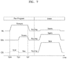
- FIGS. 4 to 8 are timing diagrams of voltages applied to each line during a pre-program operation and an erasing operation performed by a memory device according to an exemplary embodiment of the inventive concept.
- FIGS. 4 to 8 are timing diagrams for explaining operation S 10 and operation S 20 of FIG. 3A .
- a memory device in a pre-program operation, may apply a pre-program voltage Vprepro to word lines WL connected to a dummy string in which the pre-program operation is to be performed, a pass voltage Vpass to a ground selection line GSL connected to the dummy string, and a first common source line voltage (for example, the ground voltage Vss) to the common source line CSL.
- a substrate for example, the SUB of FIG. 3
- a section in which the pre-program voltage Vprepro is applied to the word lines WL and a section in which the pass voltage Vpass is applied to the ground selection line GSL may overlap.
- the pass voltage Vpass may be applied to the ground selection line GSL.
- the ground selection line GSL may float at the pass voltage Vpass.
- the section in which the pre-program voltage Vprepro is applied to the word lines WL may match with the section in which the pass voltage Vpass is applied to the ground selection line GSL.
- the pre-program voltage Vprepro and the pass voltage Vpass may be applied at the same time.
- the section in which the pre-program voltage Vprepro is applied to the word lines WL and the section in which the first common source line voltage (for example, the ground voltage Vss) is applied to the common source line CSL may overlap.
- the ground voltage Vss may be applied to the common source line CSL.
- the common source line CSL may float at the ground voltage Vss.
- the section in which the pre-program voltage Vprepro is applied to the word lines WL may match with the section in which the ground voltage Vss is applied to the common source line CSL.
- the pre-program voltage Vprepro and the ground voltage Vss may be applied at the same time.
- the memory device 100 may apply a word line erasing voltage Vwers to the word lines WL, may apply a ground erasing voltage Vgers to the ground selection line GSL, and may apply an erasing voltage Vers to the common source line CSL.
- the word line erasing voltage Vwers may be the ground voltage Vss or may have a level close to the ground voltage Vss.
- the intensity of the ground erasing voltage Vgers may be lower than that of the erasing voltage Vers by a certain level.
- the memory device 100 may, depending on the level of the erasing voltage Vers applied to the common source line CSL, apply the ground erasing voltage Vgers to the ground selection line GSL.
- the erasing voltage Vers may be applied to the substrate SUB.
- the section in which the pre-program voltage Vprepro is applied to the word lines WL and the section in which the pass voltage Vpass is applied to the ground selection line GSL may overlap.
- the time point Tgf at which the ground selection line GSL floats at the pass voltage Vpass may differ from a time point Tpf at which the word lines WL float at the pre-program voltage Vprepro.
- the time point Tgf at which the ground selection line GSL floats at the pass voltage Vpass may occur before the time point Tpf at which the word lines WL float at the pre-program voltage Vprepro.
- the section in which the pass voltage Vpass is applied to the ground selection line GSL may be shorter than the section in which the pre-program voltage Vprepro is applied to the word lines WL.
- the pass voltage Vpass may be applied for a shorter amount of time than the pre-program voltage Vprepro.
- the section in which the pass voltage Vpass is applied to the ground selection line GSL may be longer than the section in which the pre-program voltage Vprepro is applied to the word lines WL.
- the pass voltage Vpass may be applied for a longer amount of time than the pre-program voltage Vprepro.
- the section in which the pre-program voltage Vprepro is applied to the word lines WL and the section in which the pass voltage Vpass is applied to the ground selection line GSL may overlap.
- the time point Tpre at which the pre-program voltage Vprepro is applied to the word lines WL may differ from a time point Tgp at which the pass voltage Vpass is applied to the ground selection line GSL.
- the time point Tpre at which the pre-program voltage Vprepro is applied to word lines the WL may occur before the time point Tgp at which the pass voltage Vpass is applied to the ground selection line GSL.
- the section in which the pass voltage Vpass is applied to the ground selection line GSL may be shorter than the section in which the pre-program voltage Vprepro is applied to the word lines WL.
- the section in which the pass voltage Vpass is applied to the ground selection line GSL may be longer than the section in which the pre-program voltage Vprepro is applied to the word lines WL.
- the section in which the pre-program voltage Vprepro is applied to the word lines WL and the section in which the first common source line voltage (for example, the ground voltage Vss) is applied to the common source line CSL may overlap.
- the time point Tpre in which the pre-program voltage Vprepro is applied to the word lines WL may differ from a time point Tgp at which the ground voltage Vss is applied to the common source line CSL.
- the ground voltage Vss may be applied to the common source line CSL, and at the time point Tgp at which the pass voltage Vpass is applied to the ground selection line GSL, the ground voltage Vss may be applied to the common source line CSL.
- the section in which the ground voltage Vss is applied to the common source line CSL may be shorter than the section in which the pre-program voltage Vprepro is applied to word lines WL. In other words, the ground voltage Vss may be applied for a shorter amount of time than the pre-program voltage Vprepro.
- the section in which the ground voltage Vss is applied to the common source line CSL and the section in which the pass voltage Vpass is applied to the ground selection line GSL may overlap, for example, may match with each other. For example, the ground voltage Vss and the pass voltage Vpass may be applied for the same amount of time. In an exemplary embodiment of the inventive concept, however, the section in which the ground voltage Vss is applied to the common source line CSL may be longer than the section in which the pre-program voltage Vprepro is applied to the word lines WL.
- a second common source line voltage Vcs 1 may be applied to the common source line CSL.
- the application of the second common source line voltage Vcs 1 to the common source line CSL may prevent any damage to the common source line CSL due to the pre-program operation.
- the section in which the pre-program voltage Vprepro is applied to the word lines WL and the section in which the first common source line voltage (for example, the ground voltage Vss) is applied to the common source line CSL may overlap.
- the time point Tpre in which the pre-program voltage Vprepro is applied to the word lines WL may differ from the time point at which the ground voltage Vss is applied to the common source line CSL.
- the ground voltage Vss may be applied to the common source line CSL.
- the ground voltage Vss may be applied to the common source line CSL, and after a certain period of time, the second common source line voltage Vcs 1 may be applied to the common source line CSL.
- the second common source line voltage Vcs 1 may be applied to the common source line CSL.
- the section in which the ground voltage Vss is applied to the common source line CSL may be shorter than the section in which the pre-program voltage Vprepro is applied to the word lines WL.
- the section in which the ground voltage Vss is applied to the common source line CSL and the section in which the pass voltage Vpass is applied to the ground selection line GSL may overlap.
- the pass voltage Vpass and the ground voltage Vss may be applied at the same time.
- the section in which the ground voltage Vss is applied to the common source line CSL may be longer than the section in which the pre-program voltage Vprepro is applied to word lines WL.
- the inventive concept is not limited to the pre-program operations described in connection with FIGS. 4 and 8 .
- the section in which the pre-program voltage Vprepro is applied to the word lines WL, the section in which the pass voltage Vpass is applied to the ground selection line GSL, and the section in which the ground voltage Vss is applied to the common source line CSL may overlap.
- the time point Tpre at which the pre-program voltage Vprepro is applied to the word lines WL and the length of the section in which the pre-program voltage Vprepro is applied to the word lines WL may vary
- the time point at which the pass voltage Vpass is applied to the ground selection line GSL and the length of the section in which the pass voltage Vpass is applied to the ground selection line GSL may vary
- the time point at which the ground voltage Vss is applied to the common source line CSL and the length of the section in which the ground voltage Vss is applied to the common source line CSL may vary.
- FIG. 9 is a cross-sectional view illustrating memory blocks included in a memory device according to an exemplary embodiment of the inventive concept.
- FIG. 9 shows a cross-section taken along the line A-A′ illustrated in FIG. 2A .
- the description provided in connection with FIG. 2B may be omitted.
- a ground selection line GSL, a dummy word line DWL 1 , a plurality of word lines WL 1 to WL 7 , and a string selection line SSL may be arranged on a substrate SUB.
- the dummy word line DWL 1 may be arranged adjacent to the ground selection line GSL.
- one dummy word line and seven word lines are illustrated in FIG. 9 , the inventive concept is not limited thereto. The numbers of dummy word lines and word lines may vary.
- the dummy word line DWL 1 may be arranged adjacent to the string selection line SSL.
- the dummy hole DH 1 and each of the plurality of word lines WL 1 to WL 7 may form dummy cells DC.
- the dummy hole DH 1 and the word line WL 1 may form a dummy cell DC.
- the dummy hole DH 1 and the dummy word line DWL 1 may form a dummy cell DCa
- each of the main holes H 11 , H 31 , H 61 , and H 81 and the dummy word line DWL 1 may form a dummy cell DCb.
- the dummy cells DC, DCa, and DCb may be memory cells in which no data is written.
- the main cells MC formed in each of the main holes H 11 , H 31 , H 61 , and H 81 , the dummy cell DCb, a ground selection transistor, and a string selection transistor may constitute one cell string per hole.
- the dummy cells DC and DCa formed in the dummy hole DH 1 , the ground selection transistor, and the string selection transistor may constitute one dummy string.
- the dummy cells DC and DCa formed in the dummy hole DH 1 are not connected to the bit lines BL 1 , BL 3 , BL 6 and BL 8 , the dummy cells DC and DCa may not be programmed when a voltage is applied to the bit lines BL 1 , BL 3 , BL 6 , and BL 8 .
- the dummy cells DC and DCa formed in the dummy hole DH 1 may be pre-programmed by applying a ground voltage to a common source line, a pass voltage to the ground selection line GSL, and a pre-program voltage to the word lines WL 1 to WL 7 .
- a ground voltage may be applied to a substrate SUB.
- a memory device may pre-program at least some of the dummy cells DC and DCa formed in the dummy hole DH 1 by selectively applying a pre-program voltage to at least some of the dummy word line DWL 1 and the word lines WL 1 to WL 7 .
- the case in which the pre-program voltage is selectively applied to some of the dummy word line DWL 1 and word lines WL 1 to WL 7 will be described in connection with FIGS. 10B and 10C .
- the main cells MC are also pre-programmed together with the dummy cells DC and DCa.
- the dummy cells DCb formed in the main holes H 11 , H 31 , H 61 , and H 81 , not the dummy hole DH 1 may be pre-programmed.
- FIGS. 10A through 10C are tables illustrating voltage conditions applied to word lines and dummy word lines when a memory device according to an exemplary embodiment of the inventive concept performs a pre-program operation.
- a memory device may apply a pre-program voltage to the word lines WL and the dummy word line DWL 1 .
- the memory device 100 may apply a pre-program voltage Vprepro to all word lines (for example, first to seventh word lines WL 1 to WL 7 and the dummy word line DWL 1 ), connected to a dummy string on which a pre-program operation is to be performed.
- the pre-program operation may be performed on all main cells and dummy cells included in a memory block.
- the memory device 100 may apply a pass voltage to a ground selection line GSL connected to the dummy string and a ground voltage to a common source line CSL, to perform the pre-program operation.
- the description provided in connection with FIGS. 4 to 8 may be applicable to the time point at which the pass voltage is applied to the ground selection line GSL and the time point at which the ground voltage is applied to the common source line CSL.
- the memory device 100 may apply the pre-program voltage to the dummy word line DWL 1 which is selected to perform the pre-program operation, and the word line pass voltage Vwp to an unselected word line.
- the memory device 100 may selectively perform a pre-program operation.
- the memory device 100 may perform a pre-program operation on the dummy cells DCa and DCb connected to the dummy word line DWL 1 and may not perform the pre-program operation on the main cells MC.
- the level of the word line pass voltage Vwp may be lower than the level of the pre-program voltage Vprepro.
- the memory device 100 may apply the pre-program voltage Vprepro to the word lines WL and apply the word line pass voltage Vwp to the dummy word line DWL 1 .
- the memory device 100 may apply a pre-program voltage Vprepro to the dummy word line DWL 1 and some of the word lines WL, and may apply the word line pass voltage Vwp to the other word lines WL, the other word lines WL being the word lines WL that do not receive the pre-program voltage Vprepro.
- the memory device 100 may selectively apply the pre-program voltage Vprepro to the dummy word line DWL 1 and lines arranged close to the substrate SUB from among the word lines WL.
- the memory device 100 may select the dummy word line DWL 1 and the word lines WL 1 and WL 2 and apply the pre-program voltage Vprepro thereto.
- the word line pass voltage Vwp may be applied to the word lines WL 3 to WL 7 arranged farther from the substrate SUB than the word lines WL 1 and WL 2 .
- a memory cell positioned at a lower level adjacent to the substrate SUB may be more likely damaged.
- the memory device 100 may prevent memory cells from being damaged by performing a pre-program operation on memory cells positioned at a lower level adjacent to the substrate SUB.
- the pre-program voltage Vprepro is applied to the dummy word line DWL 1 .
- the inventive concept is not limited thereto.
- the word line pass voltage Vwp may be applied to the dummy word line DWL 1
- the pre-program voltage Vprepro may be applied to at least some of the word lines WL.
- FIGS. 11A and 11B are views for explaining a first memory block illustrated in FIG. 1 , according to an exemplary embodiment of the inventive concept.
- FIG. 11A is a top view of the first memory block illustrated in FIG. 1 .
- FIG. 11B illustrates a cross-section taken along the line C-C′ illustrated in FIG. 11A . In the embodiments described in connection with FIG. 11B , the corresponding descriptions provided in connection with FIG. 2B may be omitted.
- FIG. 11B illustrates region D of FIG. 11A in more detail.
- a memory block BLK 1 ′ may include a plurality of vertical holes (for example, the main holes H 11 , H 31 , H 61 , and H 81 and the dummy hole DH 1 in FIG. 11B ) arranged in the first direction X and the second direction Y between the word line cut regions WLC.
- the number of vertical holes included in the memory block BLK 1 ′ may vary.
- the memory block BLK 1 ′ may be connected to bit lines BL 1 to BL 8 and a dummy bit line DBL extending in the second direction Y and spaced apart from each other in the first direction X.
- the main holes H 11 , H 31 , H 61 , and H 81 may be respectively connected to corresponding bit lines BL 1 , BL 3 , BL 6 and BL 8
- the dummy hole DH may be connected to the dummy bit line DBL.
- the memory block BLK 1 ′ includes eight bit lines including the bit lines BL 1 to BL 8 and one dummy bit line including the dummy bit line DBL.
- the inventive concept is not limited thereto, and the number of bit lines and the number of dummy bit lines vary.
- each of the main holes H 11 , H 31 , H 61 , and H 81 and each of the word lines WL 1 to WL 8 may form main cells MC, and the main holes H 11 , H 31 , H 61 , and H 81 may be respectively connected to the bit lines BL 1 , BL 3 , BL 6 , and BL 8 .
- the main cells MC formed in each of the main holes H 11 , H 31 , H 61 , and H 81 , a ground selection transistor, and a string selection transistor may constitute one cell string per hole.
- the dummy hole DH 1 and each of the word lines WL 1 to WL 8 may form dummy cells DC, and the dummy hole DH 1 may be connected to the dummy bit line DBL.
- the dummy cells DC formed in the dummy hole DH 1 , the ground selection transistor, and the string selection transistor may constitute one dummy string.
- the memory device 100 may selectively pre-program memory cells included in a cell string or a dummy string by selectively applying a bit line program voltage to the bit lines BL 1 , BL 3 , BL 6 , and BL 8 and the dummy bit line DBL.
- a bit line program voltage to the bit lines BL 1 , BL 3 , BL 6 , and BL 8 and the dummy bit line DBL.
- FIGS. 12A and 12B are tables illustrating voltage conditions applied to bit lines and dummy bit lines when a memory device according to an exemplary embodiment of the inventive concept performs a pre-program operation.
- FIGS. 12A and 12B are views for explaining a pre-program operation selectively performed on at least some of a plurality of strings by controlling a bit line voltage.
- a memory device may apply a bit line program voltage Vbpro to bit lines (BL, for example, BL 1 , BL 3 , BL 6 , and BL 8 ) and the dummy bit line DBL during a pre-program operation (for example, operation S 10 of FIG. 3A ).
- a pre-program operation may be performed on cell strings connected to the bit lines BL and formed in the main holes H 11 , H 31 , H 61 , and H 81 , and a dummy string connected to the dummy bit line DBL and formed in the dummy hole DH 1 .
- the memory device 100 may apply a pre-program voltage Vprepro to at least some of the word lines WL, a pass voltage to the ground selection line GSL connected to a dummy string, and a ground voltage to the common source line CSL.
- Vprepro a pre-program voltage
- the description provided in connection with FIGS. 4 to 8 may be applicable to the time point at which the pass voltage is applied to the ground selection line GSL and the time point at which the ground voltage is applied to the common source line CSL.
- the memory device 100 may selectively perform a pre-program operation on a dummy string (for example, a dummy string formed in the dummy hole DH 1 ) from among a plurality of strings.
- the memory device 100 may not perform the pre-program operation on cell strings (for example, cell strings formed in the main holes H 11 , H 31 , H 61 , and H 81 ).
- the memory device 100 may apply the bit line program voltage Vbpro to the dummy bit line DBL, and a program inhibition voltage Vbinh to the bit lines BL 1 , BL 3 , BL 6 , and BL 8 connected to the cell strings.
- the level of the program inhibition voltage Vbinh may be greater than the level of the bit line program voltage Vbpro.
- the bit line program voltage Vbpro may be a ground voltage and the program inhibition voltage Vbinh may be a power voltage.
- the pre-program operation is selectively performed on a dummy string.
- the selective pre-program operation may be formed on at least some of the cell strings.
- the memory device 100 may apply a bit line program voltage Vbpro to at least some of the cell strings.
- the memory device 100 may selectively perform a pre-program operation on a dummy string from among a plurality of strings by applying the bit line program voltage Vbpro to the dummy bit line DBL. Since data may be written on the main cells MC included in cell strings, separate program operations may be performed. On the other hand, since the program operation in which data is written is not performed on the dummy cells DC included in the dummy string, damage to the dummy string may be prevented by performing a separate pre-program operation on the dummy string before or after the erasing operation.
- FIG. 13 is a block diagram illustrating a memory device according to exemplary embodiments of the inventive concept is applied to a solid state drive (SSD) system 1000 .
- SSD solid state drive
- the SSD system 1000 may include a host 1100 and an SSD 1200 .
- the SSD 1200 transmits and receives signals SIG to and from the host 1100 through a signal connector, and receives power PWR through a power connector.
- the SSD 1200 may include an SSD controller 1210 , an auxiliary power supply 1220 , and memory devices 1230 , 1240 and 1250 .
- the memory devices 1230 , 1240 and 1250 may be flash memory devices.
- the memory devices 1230 , 1240 and 1250 may be connected to the SSD controller 1210 through channels Ch 1 , Ch 2 , . . . Chn.
- the SSD 1200 may be implemented by the embodiments described above with reference to FIGS. 1 through 12B .
- Each of the memory devices 1230 , 1240 and 1250 includes dummy cells included in a dummy string and may perform a pre-program operation on the dummy string before or after an erasing operation. Thus, it is possible to prevent the dummy string from being damaged due to repetitive erasing operations.
- Exemplary embodiments of the inventive concept provide a vertical memory device that can prevent damage to a dummy string due to repeatedly performed erasing operations, and an operating method thereof.
Landscapes
- Engineering & Computer Science (AREA)
- Microelectronics & Electronic Packaging (AREA)
- Computer Hardware Design (AREA)
- Read Only Memory (AREA)
- Non-Volatile Memory (AREA)
Abstract
Description
Claims (20)
Applications Claiming Priority (2)
| Application Number | Priority Date | Filing Date | Title |
|---|---|---|---|
| KR10-2019-0023285 | 2019-02-27 | ||
| KR1020190023285A KR102723993B1 (en) | 2019-02-27 | 2019-02-27 | Vertical memory device and method of operation thereof |
Publications (2)
| Publication Number | Publication Date |
|---|---|
| US20200273522A1 US20200273522A1 (en) | 2020-08-27 |
| US11043273B2 true US11043273B2 (en) | 2021-06-22 |
Family
ID=72141804
Family Applications (1)
| Application Number | Title | Priority Date | Filing Date |
|---|---|---|---|
| US16/581,917 Active US11043273B2 (en) | 2019-02-27 | 2019-09-25 | Vertical memory device and an operating method thereof |
Country Status (3)
| Country | Link |
|---|---|
| US (1) | US11043273B2 (en) |
| KR (1) | KR102723993B1 (en) |
| CN (1) | CN111627480B (en) |
Families Citing this family (7)
| Publication number | Priority date | Publication date | Assignee | Title |
|---|---|---|---|---|
| US11017838B2 (en) * | 2016-08-04 | 2021-05-25 | Samsung Electronics Co., Ltd. | Nonvolatile memory devices |
| KR20220129378A (en) | 2021-03-16 | 2022-09-23 | 삼성전자주식회사 | Nonvolatile memory device and method of operation thereof |
| EP4060669A1 (en) * | 2021-03-16 | 2022-09-21 | Samsung Electronics Co., Ltd. | Nonvolatile memory device and operation method thereof |
| JP2023028175A (en) * | 2021-08-18 | 2023-03-03 | キオクシア株式会社 | semiconductor storage device |
| KR20230106371A (en) * | 2022-01-06 | 2023-07-13 | 에스케이하이닉스 주식회사 | Memory device and manufacturing method of the memory device |
| CN114783479A (en) * | 2022-04-20 | 2022-07-22 | 长江存储科技有限责任公司 | Method for operating a memory device and memory device |
| KR20240017546A (en) | 2022-08-01 | 2024-02-08 | 에스케이하이닉스 주식회사 | Memory device and operating method of the memory device |
Citations (13)
| Publication number | Priority date | Publication date | Assignee | Title |
|---|---|---|---|---|
| KR20090124291A (en) | 2008-05-29 | 2009-12-03 | 삼성전자주식회사 | Nonvolatile Memory Device and Its Program Method |
| US7974130B2 (en) | 2006-11-28 | 2011-07-05 | Kabushiki Kaisha Toshiba | Semiconductor memory device and method for erasing the same |
| US8379456B2 (en) | 2009-10-14 | 2013-02-19 | Samsung Electronics Co., Ltd. | Nonvolatile memory devices having dummy cell and bias methods thereof |
| US8976592B2 (en) | 2012-04-19 | 2015-03-10 | Samsung Electronics Co., Ltd. | Nonvolatile memory device with flag cells and user device including the same |
| US9013923B2 (en) | 2011-09-20 | 2015-04-21 | SK Hynix Inc. | Semiconductor device and operating method thereof |
| US9214237B2 (en) * | 2009-09-16 | 2015-12-15 | Kabushiki Kaisha Toshiba | Nonvolatile semiconductor memory device |
| US20170117056A1 (en) * | 2015-10-22 | 2017-04-27 | Samsung Electronics Co., Ltd. | Memory device and an edge word line management method thereof |
| US9685235B2 (en) | 2015-11-14 | 2017-06-20 | SK Hynix Inc. | Method of initializing 3D non-volatile memory device |
| US9721664B2 (en) | 2014-04-14 | 2017-08-01 | Samsung Electronics Co., Ltd. | Memory devices and methods of operating the memory devices by programming normal cells after programming a first dummy cell |
| US9792992B1 (en) | 2016-03-25 | 2017-10-17 | SK Hynix Inc. | Semiconductor device and operating method thereof |
| US20180059937A1 (en) | 2016-08-25 | 2018-03-01 | SK Hynix Inc. | Memory system and operating method thereof |
| US9916900B2 (en) * | 2015-08-25 | 2018-03-13 | Samsung Electronics Co., Ltd. | Memory device, memory system, method of operating memory device, and method of operating memory system |
| US9997248B2 (en) | 2016-11-15 | 2018-06-12 | SK Hynix Inc. | Semiconductor memory device and method of operating the same |
Family Cites Families (7)
| Publication number | Priority date | Publication date | Assignee | Title |
|---|---|---|---|---|
| US7505321B2 (en) * | 2002-12-31 | 2009-03-17 | Sandisk 3D Llc | Programmable memory array structure incorporating series-connected transistor strings and methods for fabrication and operation of same |
| KR20100013955A (en) * | 2008-08-01 | 2010-02-10 | 주식회사 하이닉스반도체 | Method of programming a non-volatile memory device |
| JP5238734B2 (en) * | 2010-02-10 | 2013-07-17 | 株式会社東芝 | Semiconductor device and control method thereof |
| KR20150091687A (en) * | 2014-02-03 | 2015-08-12 | 에스케이하이닉스 주식회사 | Semiconductor apparatus |
| KR102324797B1 (en) * | 2015-09-17 | 2021-11-11 | 삼성전자주식회사 | Non-volatile memory device and operating method thereof |
| KR102356741B1 (en) * | 2017-05-31 | 2022-01-28 | 삼성전자주식회사 | Semiconductor device including insulating layers and method of forming the same |
| KR102307063B1 (en) * | 2017-06-26 | 2021-10-01 | 삼성전자주식회사 | Memory device |
-
2019
- 2019-02-27 KR KR1020190023285A patent/KR102723993B1/en active Active
- 2019-09-25 US US16/581,917 patent/US11043273B2/en active Active
-
2020
- 2020-02-26 CN CN202010118717.1A patent/CN111627480B/en active Active
Patent Citations (13)
| Publication number | Priority date | Publication date | Assignee | Title |
|---|---|---|---|---|
| US7974130B2 (en) | 2006-11-28 | 2011-07-05 | Kabushiki Kaisha Toshiba | Semiconductor memory device and method for erasing the same |
| KR20090124291A (en) | 2008-05-29 | 2009-12-03 | 삼성전자주식회사 | Nonvolatile Memory Device and Its Program Method |
| US9214237B2 (en) * | 2009-09-16 | 2015-12-15 | Kabushiki Kaisha Toshiba | Nonvolatile semiconductor memory device |
| US8379456B2 (en) | 2009-10-14 | 2013-02-19 | Samsung Electronics Co., Ltd. | Nonvolatile memory devices having dummy cell and bias methods thereof |
| US9013923B2 (en) | 2011-09-20 | 2015-04-21 | SK Hynix Inc. | Semiconductor device and operating method thereof |
| US8976592B2 (en) | 2012-04-19 | 2015-03-10 | Samsung Electronics Co., Ltd. | Nonvolatile memory device with flag cells and user device including the same |
| US9721664B2 (en) | 2014-04-14 | 2017-08-01 | Samsung Electronics Co., Ltd. | Memory devices and methods of operating the memory devices by programming normal cells after programming a first dummy cell |
| US9916900B2 (en) * | 2015-08-25 | 2018-03-13 | Samsung Electronics Co., Ltd. | Memory device, memory system, method of operating memory device, and method of operating memory system |
| US20170117056A1 (en) * | 2015-10-22 | 2017-04-27 | Samsung Electronics Co., Ltd. | Memory device and an edge word line management method thereof |
| US9685235B2 (en) | 2015-11-14 | 2017-06-20 | SK Hynix Inc. | Method of initializing 3D non-volatile memory device |
| US9792992B1 (en) | 2016-03-25 | 2017-10-17 | SK Hynix Inc. | Semiconductor device and operating method thereof |
| US20180059937A1 (en) | 2016-08-25 | 2018-03-01 | SK Hynix Inc. | Memory system and operating method thereof |
| US9997248B2 (en) | 2016-11-15 | 2018-06-12 | SK Hynix Inc. | Semiconductor memory device and method of operating the same |
Also Published As
| Publication number | Publication date |
|---|---|
| KR102723993B1 (en) | 2024-10-30 |
| US20200273522A1 (en) | 2020-08-27 |
| KR20200104668A (en) | 2020-09-04 |
| CN111627480B (en) | 2025-06-03 |
| CN111627480A (en) | 2020-09-04 |
Similar Documents
| Publication | Publication Date | Title |
|---|---|---|
| US11043273B2 (en) | Vertical memory device and an operating method thereof | |
| US10720218B2 (en) | Nonvolatile memory device and an erase method thereof | |
| KR100909968B1 (en) | Three-dimensional flash memory device with improved driving method and driving method | |
| CN109961820B (en) | Nonvolatile memory device and method of programming therein | |
| US10325658B2 (en) | Non-volatile memory device and programming method thereof | |
| JP5090712B2 (en) | Programming method for flash memory device | |
| JP5378650B2 (en) | Flash memory device including dummy cells | |
| CN109545260B (en) | Non-volatile memory device and method of programming non-volatile memory device | |
| US11676646B2 (en) | Method of reducing program disturbance in memory device and memory device utilizing same | |
| US11594295B2 (en) | Nonvolatile memory device and method of operating the same | |
| US11367487B2 (en) | Nonvolatile memory device and erase method thereof | |
| CN111916129B (en) | Nonvolatile memory device, method of operating the same, and memory system | |
| US7768833B2 (en) | Method of programming non-volatile memory device | |
| US11322205B2 (en) | Non-volatile memory device and method for programming the same | |
| US20250095745A1 (en) | Block selection circuit controlling series connected pass transistors and flash memory including the same | |
| JP5706350B2 (en) | Nonvolatile semiconductor memory device | |
| CN118280421A (en) | Flash memory and read recovery operation method thereof |
Legal Events
| Date | Code | Title | Description |
|---|---|---|---|
| AS | Assignment |
Owner name: SAMSUNG ELECTRONICS CO., LTD., KOREA, REPUBLIC OF Free format text: ASSIGNMENT OF ASSIGNORS INTEREST;ASSIGNORS:SHIN, CHANG-HWAN;SONG, CHEOL;LEE, CHANG-SUB;REEL/FRAME:050483/0566 Effective date: 20190722 |
|
| FEPP | Fee payment procedure |
Free format text: ENTITY STATUS SET TO UNDISCOUNTED (ORIGINAL EVENT CODE: BIG.); ENTITY STATUS OF PATENT OWNER: LARGE ENTITY |
|
| STPP | Information on status: patent application and granting procedure in general |
Free format text: RESPONSE TO NON-FINAL OFFICE ACTION ENTERED AND FORWARDED TO EXAMINER |
|
| STPP | Information on status: patent application and granting procedure in general |
Free format text: NOTICE OF ALLOWANCE MAILED -- APPLICATION RECEIVED IN OFFICE OF PUBLICATIONS |
|
| STPP | Information on status: patent application and granting procedure in general |
Free format text: PUBLICATIONS -- ISSUE FEE PAYMENT RECEIVED |
|
| STPP | Information on status: patent application and granting procedure in general |
Free format text: PUBLICATIONS -- ISSUE FEE PAYMENT VERIFIED |
|
| STCF | Information on status: patent grant |
Free format text: PATENTED CASE |
|
| MAFP | Maintenance fee payment |
Free format text: PAYMENT OF MAINTENANCE FEE, 4TH YEAR, LARGE ENTITY (ORIGINAL EVENT CODE: M1551); ENTITY STATUS OF PATENT OWNER: LARGE ENTITY Year of fee payment: 4 |