US11006064B2 - CMOS image sensor and method of operating pixel array by CMOS image sensor - Google Patents
CMOS image sensor and method of operating pixel array by CMOS image sensor Download PDFInfo
- Publication number
- US11006064B2 US11006064B2 US16/571,217 US201916571217A US11006064B2 US 11006064 B2 US11006064 B2 US 11006064B2 US 201916571217 A US201916571217 A US 201916571217A US 11006064 B2 US11006064 B2 US 11006064B2
- Authority
- US
- United States
- Prior art keywords
- transistor
- readout
- image sensor
- cmos image
- signal
- Prior art date
- Legal status (The legal status is an assumption and is not a legal conclusion. Google has not performed a legal analysis and makes no representation as to the accuracy of the status listed.)
- Active
Links
- 238000000034 method Methods 0.000 title claims abstract description 8
- 239000003990 capacitor Substances 0.000 claims description 41
- 238000009792 diffusion process Methods 0.000 description 23
- 238000010586 diagram Methods 0.000 description 20
- 102100033126 Phosphatidate cytidylyltransferase 2 Human genes 0.000 description 13
- 101710178746 Phosphatidate cytidylyltransferase 2 Proteins 0.000 description 13
- 230000003071 parasitic effect Effects 0.000 description 10
- 206010034960 Photophobia Diseases 0.000 description 8
- 208000013469 light sensitivity Diseases 0.000 description 8
- 230000000875 corresponding effect Effects 0.000 description 6
- 238000005286 illumination Methods 0.000 description 6
- 230000010354 integration Effects 0.000 description 6
- 101100328883 Arabidopsis thaliana COL1 gene Proteins 0.000 description 4
- 101100328886 Caenorhabditis elegans col-2 gene Proteins 0.000 description 4
- 230000002596 correlated effect Effects 0.000 description 3
- 238000005070 sampling Methods 0.000 description 3
- 239000004065 semiconductor Substances 0.000 description 3
- 230000004075 alteration Effects 0.000 description 1
- 230000015572 biosynthetic process Effects 0.000 description 1
- 230000015556 catabolic process Effects 0.000 description 1
- 238000010276 construction Methods 0.000 description 1
- 238000006731 degradation reaction Methods 0.000 description 1
- 230000005670 electromagnetic radiation Effects 0.000 description 1
- 230000003595 spectral effect Effects 0.000 description 1
- 238000006467 substitution reaction Methods 0.000 description 1
Images


Classifications
-
- H04N5/378—
-
- H—ELECTRICITY
- H04—ELECTRIC COMMUNICATION TECHNIQUE
- H04N—PICTORIAL COMMUNICATION, e.g. TELEVISION
- H04N25/00—Circuitry of solid-state image sensors [SSIS]; Control thereof
- H04N25/60—Noise processing, e.g. detecting, correcting, reducing or removing noise
- H04N25/616—Noise processing, e.g. detecting, correcting, reducing or removing noise involving a correlated sampling function, e.g. correlated double sampling [CDS] or triple sampling
-
- H01L27/14634—
-
- H01L27/14643—
-
- H—ELECTRICITY
- H04—ELECTRIC COMMUNICATION TECHNIQUE
- H04N—PICTORIAL COMMUNICATION, e.g. TELEVISION
- H04N25/00—Circuitry of solid-state image sensors [SSIS]; Control thereof
- H04N25/70—SSIS architectures; Circuits associated therewith
- H04N25/76—Addressed sensors, e.g. MOS or CMOS sensors
-
- H—ELECTRICITY
- H04—ELECTRIC COMMUNICATION TECHNIQUE
- H04N—PICTORIAL COMMUNICATION, e.g. TELEVISION
- H04N25/00—Circuitry of solid-state image sensors [SSIS]; Control thereof
- H04N25/70—SSIS architectures; Circuits associated therewith
- H04N25/76—Addressed sensors, e.g. MOS or CMOS sensors
- H04N25/77—Pixel circuitry, e.g. memories, A/D converters, pixel amplifiers, shared circuits or shared components
- H04N25/771—Pixel circuitry, e.g. memories, A/D converters, pixel amplifiers, shared circuits or shared components comprising storage means other than floating diffusion
-
- H—ELECTRICITY
- H04—ELECTRIC COMMUNICATION TECHNIQUE
- H04N—PICTORIAL COMMUNICATION, e.g. TELEVISION
- H04N25/00—Circuitry of solid-state image sensors [SSIS]; Control thereof
- H04N25/70—SSIS architectures; Circuits associated therewith
- H04N25/76—Addressed sensors, e.g. MOS or CMOS sensors
- H04N25/78—Readout circuits for addressed sensors, e.g. output amplifiers or A/D converters
-
- H04N5/359—
-
- H04N5/374—
-
- H—ELECTRICITY
- H10—SEMICONDUCTOR DEVICES; ELECTRIC SOLID-STATE DEVICES NOT OTHERWISE PROVIDED FOR
- H10F—INORGANIC SEMICONDUCTOR DEVICES SENSITIVE TO INFRARED RADIATION, LIGHT, ELECTROMAGNETIC RADIATION OF SHORTER WAVELENGTH OR CORPUSCULAR RADIATION
- H10F39/00—Integrated devices, or assemblies of multiple devices, comprising at least one element covered by group H10F30/00, e.g. radiation detectors comprising photodiode arrays
- H10F39/10—Integrated devices
- H10F39/12—Image sensors
- H10F39/18—Complementary metal-oxide-semiconductor [CMOS] image sensors; Photodiode array image sensors
-
- H—ELECTRICITY
- H10—SEMICONDUCTOR DEVICES; ELECTRIC SOLID-STATE DEVICES NOT OTHERWISE PROVIDED FOR
- H10F—INORGANIC SEMICONDUCTOR DEVICES SENSITIVE TO INFRARED RADIATION, LIGHT, ELECTROMAGNETIC RADIATION OF SHORTER WAVELENGTH OR CORPUSCULAR RADIATION
- H10F39/00—Integrated devices, or assemblies of multiple devices, comprising at least one element covered by group H10F30/00, e.g. radiation detectors comprising photodiode arrays
- H10F39/80—Constructional details of image sensors
- H10F39/809—Constructional details of image sensors of hybrid image sensors
Definitions
- CMOS image sensors In the field of CMOS image sensors, a global shutter CMOS image sensor is mostly preferred to capture fast-moving objects.
- the global shutter imager sensor is widely used in charge domain and voltage domain operations. In voltage domain, the global shutter image sensors are focused on reducing parasitic light sensitivity for backside illuminated structure, which in turn produce low signal to noise ratio and difficult to achieve the better image quality.
- the conventional charge domain global shutter can maintain the signal-to-noise ratio without signal degradation, but the high parasitic light sensitivity makes it not suitable to implement in back-side illumination structure. That is, the high image quality is not achieved because of the high parasitic light sensitivity or the low signal to noise ratio.
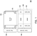
- FIG. 1 illustrates a 2D layout block diagram of a CMOS image sensor according to an exemplary embodiment of the disclosure.
- FIG. 2 illustrates a schematic circuit diagram of a CMOS image sensor according to an exemplary embodiment of the disclosure.
- FIG. 3 illustrates operation waveforms of a CMOS image sensor according to an exemplary embodiment of the disclosure.
- FIG. 4 illustrates a schematic circuit diagram of a CMOS image sensor according to another exemplary embodiment of the disclosure.
- FIG. 5 illustrates operation waveforms of a CMOS image sensor according to an exemplary embodiment of the disclosure.
- FIG. 6 illustrates a schematic circuit diagram of a CMOS image sensor according to another exemplary embodiment of the disclosure.
- FIG. 7 illustrates a schematic circuit diagram of a CMOS image sensor according to another exemplary embodiment of the disclosure.
- FIG. 8 illustrates a schematic circuit diagram of a CMOS image sensor according to another exemplary embodiment of the disclosure.
- FIG. 9 illustrates a schematic circuit diagram of a CMOS image sensor according to another exemplary embodiment of the disclosure.
- FIG. 10 illustrates a schematic circuit diagram of a CMOS image sensor according to another exemplary embodiment of the disclosure.
- FIG. 11 illustrates operation waveforms of a CMOS image sensor according to an exemplary embodiment of the disclosure.
- FIG. 12 is a flow chart illustrating a method of operating a pixel array by a CMOS image sensor according to an exemplary embodiment of the disclosure.
- FIG. 13 illustrates a 3D layout block diagram of a CMOS image sensor according to an exemplary embodiment of the disclosure.
- FIG. 14 illustrates a 3D layout block diagram of a CMOS image sensor according to an exemplary embodiment of the disclosure.
- first and second features are formed in direct contact
- additional features may be formed between the first and second features, such that the first and second features may not be in direct contact
- present disclosure may repeat reference numerals and/or letters in the various examples. This repetition is for the purpose of simplicity and clarity and does not in itself dictate a relationship between the various embodiments and/or configurations discussed.
- spatially relative terms such as “beneath,” “below,” “lower,” “above,” “upper” and the like, may be used herein for ease of description to describe one element or feature's relationship to another element(s) or feature(s) as illustrated in the figures.
- the spatially relative terms are intended to encompass different orientations of the device in use or operation in addition to the orientation depicted in the figures.
- the apparatus may be otherwise oriented (rotated 90 degrees or at other orientations) and the spatially relative descriptors used herein may likewise be interpreted accordingly.
- FIG. 1 illustrates a 2D layout block diagram of a CMOS image sensor 100 according to an exemplary embodiment of the disclosure.
- the CMOS image sensor array 100 includes a global shutter (GS) pixel array 110 , a row controller 120 , a readout circuit 130 , and a column controller 140 .
- the global shutter pixel array 110 has a plurality of pixel 115 array in M*N, where M denotes the row of the pixel array and N denotes the column of the pixel array.
- M denotes the row of the pixel array and N denotes the column of the pixel array.
- Each of the plurality of pixels (Pix) 115 in the global shutter pixel array 110 is controlled by row controller 120 and the column controller 140 .
- the row controller 120 readouts the pixel 115 when the photosensitive device receives the incident light and generates the charge corresponding to the incident light.
- the column controller 140 maps the column pixel corresponding to the row in the global shutter pixel array 110 .
- the readout circuit reads out the pixel charge/voltage in the corresponding row of the global shutter pixel array 110 .
- the readout circuit 130 includes a correlated double sampling circuit (CDS) 133 and an analog-to-digital converter (ADC) 135 .
- the readout circuit 130 reads out the charge/voltage signal and the reset signal simultaneously at the same time during the first readout operation. After the first readout operation, the common-mode signal is generated by an equalization operation, and the common mode signal is reading out by the readout circuit 130 in the second readout operation. It is noted that the first readout operation and the second readout operation do not overlap each other. Based on the above, the readout offset and the flicker noise are cancelled by double readout operation.
- FIG. 2 illustrates a schematic circuit diagram of a CMOS image sensor 200 according to an exemplary embodiment of the disclosure.
- the CMOS image sensor 200 includes a sensor 210 , a readout circuit 220 , and a column readout circuit 230 .
- the CMOS image sensor 200 is also defined as “7T” charge domain global shutter (CDGS) CMOS image sensor.
- the “7T” defines the number of active transistors presented in the structure.
- the sensor 210 is configured to generate a first charge signal and a first reset signal.
- the sensor 210 further includes a photosensitive device 215 , a transmitter transistor TX, and a reset transistor RST.
- the photosensitive device 215 is a diode that receives an incident light and generates a charge/voltage corresponds to an incident light.
- the photosensitive device 215 is presented as a photosensitive diode or the devices that are responsive to electromagnetic radiation in the visible, infrared, and/or ultraviolet spectral regions, thus the photosensitive device 215 used in the disclosure is not limited thereto.
- the transmitter transistor TX and the reset transistor RST are N-type Metal-Oxide-Semiconductor (NMOS) transistors, but a type of the transistors and number of transistors are not limited in the disclosure.
- the transmitter transistor TX is coupled to photosensitive device 215 and the reset transistor RST.
- the transmitter transistor TX receives the control signal to turn on the transmitter transistor TX, which transfers the charge accumulated in the photosensitive device 215 to a floating diffusion node V 1 .
- the floating diffusion node V 1 has an intrinsic capacitance that stores the charge accumulated in the photosensitive device 215 .
- the reset transistor RST is coupled between a power supply VDD and the floating diffusion node V 1 to reset or charge the floating diffusion node V 1 .
- the control terminal of the reset transistor RST receives the reset signal to perform the reset or charge operation.
- the readout circuit 220 further includes a first source follower 222 , a second source follower 224 and a switch SW.
- the first source follower (SF 1 ) 222 having a first transistor M 1 and a second transistor M 2 .
- the first source follower 222 is configured to perform a first readout operation in the floating diffusion node V 1 .
- the drain terminal of the first transistor M 1 and the drain terminal of the second transistor M 2 are directly coupled to each other forms a source follower circuit 222 .
- the control terminal of the first transistor M 1 receives the control signal from the floating diffusion node V 1 and the control terminal of the second transistor M 2 receives the row select signal RSL to select the row of the pixel array.
- the second source follower (SF 2 ) 224 having a third transistor M 3 and a fourth transistor M 4 . Similarly, the drain terminal of the third transistor M 3 and the drain terminal of the fourth transistor M 4 are directly coupled to each other forms a source follower circuit 224 .
- the second source follower 222 is configured to perform a second readout operation in the reset node V 2 .
- the column readout circuit 230 having a plurality of transistors M 33 , M 44 to drive the corresponding column in response to the readout operation performed by the readout circuit 220 .
- the transistors M 33 and M 44 are N-type Metal-Oxide-Semiconductor (NMOS) transistors, but the type of the transistors and the number of transistors are not limited in the disclosure.
- NMOS N-type Metal-Oxide-Semiconductor
- the first charge signal and the first reset signal are stored in separate voltage nodes, the floating diffusion node V 1 and the reset node V 2 respectively, where the integration time is time taken for the photosensitive device 215 that receives the incident light and generate the charge/voltage corresponding to the incident light.
- Both floating diffusion node V 1 and the reset node V 2 are implemented by an intrinsic capacitance or a high density MIM capacitor, hence the type of capacitor used by the floating diffusion node V 1 and the reset node V 2 are not limited thereto.
- the readout circuit 220 is configured to perform a first readout operation (CDS 1 ) by reading out a first reset signal and a first charge signal simultaneously at a first predetermined time, where the first predetermined time is the time taken to perform the first readout operation by the readout circuit 220 .
- CDS 1 first readout operation
- Equation (1) shows the column readout transistor M 33 performs the first readout operation at the floating diffusion node V 1 .
- equation (2) shows the column readout transistor M 44 performs the first readout operation at the reset node V 2 .
- the readout circuit 220 turns on the switch SW to obtain a common-mode signal by making the first reset signal equal to the first charge signal. In other words, the charge level of the first reset signal and the first charge signal are same after the first readout operation by turning on the switch SW.
- the readout circuit 220 After obtaining the common-mode signal, the readout circuit 220 re-performs a second readout operation (CD 2 ) by reading out the common-mode signal at a second predetermined time, where the second predetermined time is the time taken to perform the second readout operation by the readout circuit 220 .
- the first predetermined time and the second predetermined time are performed at different times.
- the second predetermined time is always after the first predetermined time. In other words, the first predetermined time and the second predetermined time do not overlap each other.
- V COL1 1 ⁇ 2 ⁇ ( V reset +V signal +V leak1 +V leak2 )+ V SF1,offset ⁇ (3)
- V COL2 1 ⁇ 2 ⁇ ( V reset +V signal +V leak1 +V leak2 )+ V SF2,offset ⁇ (4)
- Equation (3) shows the column readout transistor M 33 performs the second readout operation at the floating diffusion node V 1 .
- equation (4) shows that the column readout transistor M 44 performs the second readout operation at the reset node V 2 .
- the readout circuit 230 reads out the floating diffusion node V 1 and the reset node V 2 with the same charge level by turns on the switch SW after the first readout operation (CDS 1 ).
- V CDS (( V reset ⁇ V signal )+( V leak2 ⁇ V leak1 ) ⁇ (5)
- the source follower offset and the flicker noise are cancelled as shown in expression (5).
- the amount of back-side illumination structure light leakage in the floating diffusion node V 1 and the reset node V 2 are similar, therefore the light leakage is cancelled during the readout operation.
- FIG. 3 illustrates operation waveforms of a CMOS image sensor according to an exemplary embodiment of the disclosure.
- the transmitter transistor TX and the reset transistor RST are turned on to pass the charge flow from the photosensitive device 215 in the sensor 210 .
- the transmitter transistor TX, the reset transistor RST, and the switch SW are turned on to store the first charge signal and the first reset signal in separate nodes, the floating diffusion node V 1 and the reset node V 2 respectively.
- the readout circuit 230 reads out the first charge signal and the first reset signal simultaneously in the first predetermined time t 1 .
- the first readout operation is performed based on the expression (1) and (2).
- the readout circuit 220 turns on the switch SW to obtain a common-mode signal by making the first reset signal equal to the first charge signal.
- the readout circuit 220 re-performs a second readout operation (CDS 2 ) by reading out the common-mode signal at a second predetermined time t 2 .
- the first readout operation is performed based on the expression (3) and (4).
- the source follower offset and the flicker noise are cancelled as shown in expression (5).
- the amount of back-side illumination structure light leakage in the floating diffusion node V 1 and the reset node V 2 are similar, therefore the light leakage is cancelled during the readout operation.
- FIG. 4 illustrates a schematic circuit diagram of a CMOS image sensor 400 according to another exemplary embodiment of the disclosure.
- the CMOS image sensor 400 is also defined as 10T voltage domain global shutter (VDGS) CMOS image sensor.
- VDGS voltage domain global shutter
- the “10T” defines the number of active transistors presented in the structure.
- the CMOS image sensor 400 used in the exemplary embodiment is a voltage domain, thus the CMOS image sensor 400 uses voltage signal instead of charge signal with reference to FIG. 2 .
- the CMOS image sensor 400 includes a sensor 410 is similar to a sensor 210 with reference to FIG. 2 , thus the detailed description of these circuit is omitted herein.
- the transmitter transistor TX receives the control signal to turn on the transmitter transistor TX, which transfers the voltage accumulated in the photosensitive device 415 to a floating diffusion node (FD) V 1 .
- FD floating diffusion node
- the CMOS image sensor 400 further includes a readout circuit 420 , a column readout circuit 430 , a connection circuit 440 , and a bias 450 .
- the connection circuit 440 includes a connection transistor 444 is configured to couple the sensor 410 and the readout circuit 420 .
- the bias 450 having a bias transistor 455 is configured to generate a bias voltage to the CMOS image sensor 400 .
- the connection transistor 444 and the bias transistor 455 are N-type Metal-Oxide-Semiconductor (NMOS) transistors, but the type of the transistors and the number of transistors are not limited in the disclosure.
- NMOS N-type Metal-Oxide-Semiconductor
- connection transistor 444 and the bias transistor 455 forms a source follower circuit, where the drain terminal of the connection transistor 444 is directly coupled to the drain terminal of the bias transistor 455 .
- the source follower circuit formed by the connection transistor 444 and the bias transistor 455 is also defined as the first stage source follower in the CMOS image sensor 400 .
- the bias transistors 455 may turned off after the charge transfer from the source 410 to the floating diffusion node V 1 and the reset node V 2 .
- the readout circuit 420 further includes a first source follower 422 and a second source follower 424 and a plurality of switches (SW 1 , SW 2 ).
- the plurality of switches includes a first switch SW 1 and a second switch SW 2 .
- the first switch SW 1 is configured to store the first voltage signal in a first capacitor C 1 .
- the second switch SW 2 is configured to store the first reset signal in a second capacitor C 2 .
- Both the first capacitor C 1 and the second capacitor C 2 are a parasitic capacitor or a high density MIM capacitor, hence the type of capacitor used in the disclosure is not limited thereto.
- the first source follower (SF 1 ) 422 , the second source follower (SF 2 ) 424 , and the column readout circuit 430 in the exemplary embodiment is similar with reference to FIG. 2 , thus the detailed description of these circuit structures are omitted herein.
- the readout circuit 420 is configured to perform a first readout operation (CDS 1 ) by readout a first reset signal and a first voltage signal simultaneously at a first predetermined time, where the first predetermined time is the time taken to perform the first readout operation by the readout circuit 420 .
- the first predetermined time is the time taken to perform the first readout operation by the readout circuit 420 .
- the output signal of the column readout circuit 420 is calculated as in expression (1) and (2).
- the readout circuit 420 turns on the second switch SW 2 to make the first reset signal equal to the first voltage signal.
- the voltage level of the first reset signal and the first voltage signal is same after the first readout operation by turning on the second switch SW 2 to obtain a common-mode signal.
- the readout circuit 420 re-performs a second readout operation (CDS 2 ) by readout the common mode signal at a second predetermined time, where the second predetermined time is the time taken to perform the second readout operation by the readout circuit 420 .
- the first predetermined time and the second predetermined is performed at different times.
- the second predetermined time is always after the first predetermined time.
- the first predetermined time and the second predetermined time do not overlap each other.
- the output signal of the column readout circuit 420 is calculated as shown in expression (3) and (4).
- the total readout operation performed by the CMOS image sensor is calculated as ( V COL1(CDS2) ⁇ V COL1(CDS1) ) ⁇ ( V COL2(CDS2) ⁇ V COL2(CDS1) ) ⁇ (6)
- Equation (6) shows the total readout operation performed by the CMOS image sensor 400 by calculating difference between the first readout operation (CDS 1 ) and the second readout operation (CDS 2 ) performed at the floating diffusion node V 1 and the reset node V 2 .
- CDS 1 first readout operation
- CDS 2 second readout operation
- FIG. 5 illustrates operation waveforms of a CMOS image sensor according to an exemplary embodiment of the disclosure.
- a transmitter transistor TX and a reset transistor RST are turned to pass the charge flow from a photosensitive device 415 in a sensor 410 .
- the transmitter transistor TX, the reset transistor RST, a bias transistor 455 , a first switch SW 1 , and a second switch SW 2 are turned on to store the first voltage signal and the first reset signal in a first capacitor C 1 , and second capacitor C 2 .
- the charge at the first capacitor C 1 and the second capacitor C 2 are voltage signal at the floating diffusion node V 1 and the reset node V 2 respectively.
- the readout circuit 420 reads out the first voltage signal and the first reset signal simultaneously in the first predetermined time t 1 .
- the first readout operation is performed based on the expression (1) and (2).
- the readout circuit 420 turns on the second switch SW 2 to obtain a common-mode signal by making the first reset signal equal to the first voltage signal.
- the readout circuit 420 re-performs a second readout operation (CDS 2 ) by reading out the common-mode signal at a second predetermined time t 2 .
- the first readout operation is performed based on the expression (3) and (4).
- FIG. 6 illustrates a schematic circuit diagram of a CMOS image sensor 600 according to another exemplary embodiment of the disclosure.
- the CMOS image sensor 600 is also defined as 3T+7T voltage domain global shutter (VDGS) CMOS image sensor.
- VDGS voltage domain global shutter
- 3T defines the number of active transistors presented in top layer of the 3D layout
- 7T defines the number of active transistors presented in bottom layer of the 3D layout.
- the CMOS image sensor includes a sensor 610 , a readout circuit 620 , a column readout circuit 630 , a connection circuit 640 , and a bias 650 in the exemplary embodiment is similar to a sensor 410 , a readout circuit 420 , a column readout circuit 430 , a connection circuit 440 , and a bias 450 with reference to FIG. 4 , thus the detailed description of these circuits are omitted herein.
- the top layer and the bottom layer of the CMOS image sensor 600 is coupled by the 3D hybrid bond 655 located between the connection circuit 640 and the bias 650 .
- the sensor 610 and the connection circuit 640 are placed in the top layer of the 3D layout.
- the readout circuit 630 is placed in the bottom layer of the 3D layer.
- the main function of placing the circuits in the bottom layer is to give the bottom layer light shielding, which in turn may reduce the light leakage. By placing the circuits in the bottom layer shielding the amount of light leakage is negligible in addition to the parasitic light sensitivity leakage cancellation by the double readout operation.
- FIG. 7 illustrates a schematic circuit diagram of a CMOS image sensor 700 according to another exemplary embodiment of the disclosure.
- the CMOS image sensor 700 having a sensor 710 , a readout circuit 720 , a column readout circuit 730 , a connection circuit 740 , and a bias 750 in the exemplary embodiment is similar with reference to FIG. 4 , thus the detailed description of these circuits are omitted herein.
- the readout circuit 730 further includes a first source follower (SF 1 ) and a second source follower (SF 2 ) are similar with reference to FIG. 4 except for the type of transistors.
- the transistors M 1 , M 2 , M 3 and M 4 in the first source follower (SF 1 ) and the second source follower (SF 2 ) are P-type CMOS transistors, and the operation sequence of performing the first readout operation (CDS 1 ) and the second readout operation (CDS 2 ) are similar with reference to FIG. 4 .
- the transistors M 33 and M 44 in the column read circuit 730 are P-type CMOS transistors, and the operation sequence of the column readout operation performed by column read circuit 730 is similar with reference to FIG. 4 , thus the detailed description of these circuits are omitted herein.
- FIG. 8 illustrates a schematic circuit diagram of a CMOS image sensor 800 according to another exemplary embodiment of the disclosure.
- the CMOS image sensor 800 is also defined as 3T+7T voltage domain global shutter (VDGS) CMOS image sensor.
- VDGS voltage domain global shutter
- the term “3T” defines the number of active transistors presented in top layer of the 3D layout and “7T” defines the number of active transistors presented in bottom layer of the 3D layout.
- the CMOS image sensor includes a sensor 810 , a readout circuit 820 , a column readout circuit 830 , a connection circuit 840 , and a bias 850 in the exemplary embodiment is similar with reference to FIGS. 4 and 7 , thus the detailed description of the circuit is omitted herein.
- the top layer and the bottom layer of the CMOS image sensor 800 is coupled by the 3D hybrid bond 855 located between the connection circuit 840 and the bias 850 .
- the sensor 810 and the connection circuit 840 are placed in the top layer of the 3D layout.
- the readout circuit 820 is placed in the bottom layer of the 3D layer.
- the main function of placing the circuits in the bottom layer is to give the bottom layer light shielding, which in turn may reduce the light leakage. By placing the circuits in the bottom layer shielding the amount of light leakage is negligible in addition to the parasitic light sensitivity leakage cancellation by double readout operation.
- FIG. 9 illustrates a schematic circuit diagram of a CMOS image sensor 900 according to another exemplary embodiment of the disclosure.
- the CMOS image sensor 900 having a sensor 910 , a readout circuit 920 , a column readout circuit 930 , a connection circuit 940 , and a bias 950 in the exemplary embodiment is similar with reference to FIG. 4 , thus the detailed description of these circuits are omitted herein.
- the readout circuit 920 further includes a first switch SW 1 , a second switch SW 2 , a first capacitor C 1 , a second capacitor C 2 , a first unity gain buffer (UB 1 ) 922 , and a second unity gain buffer (UB 2 ) 924 .
- the circuit structure of the first switch SW 1 , the second switch SW 2 , the first capacitor C 1 , and the second capacitor C 2 is similar to the structure with reference to FIG. 4 , thus the detailed description of these circuits are omitted herein.
- the first unity gain buffer 922 having a plurality of transistors M 11 , M 12 , M 13 , M 14 , M 15 , and M 16 forms a unity gain buffer, where M 11 and M 12 are P-type CMOS transistors and other transistors are N-type CMOS transistors.
- the second unity gain buffer 924 having a plurality of transistors M 21 , M 22 , M 23 , M 24 , M 25 , and M 26 , which forms a unity gain buffer, where M 21 and M 22 are P-type CMOS transistors and other transistors are N-type CMOS transistors.
- the structure of the unity gain buffer is similar to the conventional unity gain buffer; thus, the detail description of the unity gain buffer structure and the operations are omitted herein.
- the design of unity gain buffer is not limited to the conventional structure and the structure is a determined according to the designer requirement.
- the readout operation performed by the first unity gain buffer 922 , and the second unity gain buffer 924 during the first readout operation (CDS 1 ) and the second readout operation (CDS 2 ) are similar to the readout operation performed by the first source follower (SF 1 ) and the second source follower (SF 2 ) with reference to FIG. 4 , thus the detailed description of the readout operation performed by the first unity gain buffer 922 and the second unity gain buffer 924 are omitted herein.
- FIG. 10 illustrates a schematic circuit diagram of a CMOS image sensor 1000 according to another exemplary embodiment of the disclosure.
- the CMOS image sensor 1000 having a sensor 1010 , a readout circuit 1020 , a column readout circuit 1030 , a connection circuit 1040 , and a bias 1050 in the exemplary embodiment is similar with reference to FIG. 4 , thus the detailed description of these circuits is omitted herein.
- the readout circuit 1020 further includes a first pair of switches 1021 , a second pair of switches 1022 , a first capacitor C 1 , a second capacitor C 2 , and a source follower (SF) 1025 .
- the first pair of switches having a first switch SW 1 - 1 , and a second switch SW 1 - 2 .
- the second pair of switches 1022 having a third switch SW 2 - 1 , and a fourth switch SW 2 - 2 .
- the first capacitor C 1 is coupled between the first switch SW 1 - 1 and the second switch SW 1 - 2 .
- the second capacitor C 2 is coupled between the third switch SW 2 - 1 and the fourth switch SW 2 - 2 .
- the one terminal of the first switch SW 1 - 1 and the third switch SW 2 - 1 are coupled with the connection circuit 1040 , while the other end is coupled to the first capacitor C 1 and the second capacitor C 2 respectively.
- the one terminal of the second switch SW 1 - 2 and the fourth switch SW 2 - 2 are coupled with the source follower 1025 , while the other end is coupled to the first capacitor C 1 and the second capacitor C 2 respectively.
- the first pair of switches 1021 and the second pair of switches 1022 are selectively turned on and off to charge and discharge during the readout operation.
- the source follower (SF) 1025 is similar to the first source follower (SF 1 ) with reference to FIG. 4 .
- the column readout circuit 1030 have a transistor M 33 configured to drive the corresponding column in response to the readout operation performed by the readout circuit 1020 .
- the readout circuit 1020 performs the double readout operation by selectively reading out twice by the source follower 1025 during the readout operation instead of two source followers used in exemplary embodiment with reference to FIG. 4 .
- the total readout operation performed by the CMOS image sensor is calculated as ( V COL(CDS1) ⁇ V COL(CDS2) ) ⁇ (7)
- Equation (7) shows total readout operation performed by the CMOS image sensor 1000 by calculating difference between the first readout operation (CDS 1 ) at the floating diffusion node V 1 and the reset node V 2 twice by the source follower 1025 and the second readout operation (CDS 2 ) performed at the floating diffusion node V 1 and the reset node V 2 twice by the source follower 1025 .
- the source follower offset and the flicker noise are cancelled as shown in expression (5).
- the top layer and the bottom layer of the CMOS image sensor 1000 are coupled by the 3D hybrid bond located between the connection circuit 1040 and the bias 1050 .
- the sensor 1010 and the connection circuit 1040 are placed in the top layer of the 3D layout.
- the readout circuit 1030 is placed in the bottom layer of the 3D layer.
- the main function of placing the circuits in the bottom layer is to give the bottom layer light shielding, which in turn may reduce the light leakage. By placing the circuits in the bottom layer shielding the amount of light leakage is negligible in addition to the parasitic light sensitivity leakage cancellation by double readout operation.
- FIG. 11 illustrates operation waveforms of a CMOS image sensor according to an exemplary embodiment of the disclosure.
- the transmitter transistor TX and the reset transistor RST are turned to pass the charge flow from the photosensitive device 1015 in the sensor 1010 .
- a transmitter transistor TX, a reset transistor RST, a bias transistor, a first switch SW 1 - 1 , and a third switch SW 2 - 1 are turned on to store the first voltage signal and the first reset signal in a first capacitor C 1 , and second capacitor C 2 .
- the charge at the first capacitor C 1 and the second capacitor C 2 are voltage signal at the floating diffusion node V 1 and the reset node V 2 respectively.
- the readout circuit 1020 During the first readout operation (CDS 1 ), the readout circuit 1020 , readout the first voltage signal and the first reset signal twice at the first predetermined time t 1 .
- the first readout operation is performed based on the expression (1) and (2).
- the readout circuit 1020 turns on a third switch SW 1 - 2 , and a fourth switch SW 2 - 2 to make the first reset signal equal to the first voltage signal to obtain the common-mode signal.
- the readout circuit 1020 After obtaining the common-mode signal, the readout circuit 1020 re-performs a second readout operation (CDS 2 ) by readout the common-mode signal twice at a second predetermined time t 2 .
- the first readout operation is performed based on the expression (3) and (4).
- the source follower offset and the flicker noise are cancelled as shown in expression (5).
- the amount of back-side illumination structure light leakage in each storage nodes V 1 and V 2 are similar, therefore the light leakage is cancelled during the readout operation.
- FIG. 12 is a flow chart illustrating a method of operating a pixel array by a CMOS image sensor according to an exemplary embodiment of the disclosure.
- step S 100 generating a first voltage signal and a first reset signal by a sensor.
- step S 200 storing the first voltage signal and the first reset signal in a first capacitor and a second capacitor by a readout circuit.
- step 300 performing a first readout operation by reading out the first reset signal and the first charge signal at a first predetermined time by the readout circuit. After the first readout operation, adjusting the first reset signal equal to the first voltage signal by turning on a switch by the readout circuit in step S 400 .
- step S 500 re-performing a second readout operation by reading out the first reset signal and the first voltage signal at a second predetermined time by the readout circuit.
- FIG. 13 illustrates a 3D layout block diagram of a CMOS image sensor 1300 according to an exemplary embodiment of the disclosure.
- the CMOS 1300 includes a global shutter pixel array 1310 , a row controller 1320 , a column controller 1340 , and a readout circuit 1330 in the exemplary embodiment is similar with reference to FIG. 1 .
- the top layer and the bottom layer of the CMOS image sensor 1300 is coupled by a 3D hybrid bond located between the global pixel sensor array 1310 and the readout circuit 1330 .
- the global shutter (GS) pixel sensor array 1310 is placed in the top layer and the readout circuit 1330 is placed in the bottom layer of the 3D layout.
- GS global shutter
- the main function of placing the circuits in the bottom layer is to give the bottom layer light shielding, which in turn may reduce the light leakage.
- FIG. 14 illustrates a 3D layout block diagram of a CMOS image sensor 1400 according to an exemplary embodiment of the disclosure.
- the CMOS 1400 includes a global shutter pixel array 1410 , a row controller 1420 , a column controller 1440 , and a readout circuit 1430 in the exemplary embodiment is similar with reference to FIGS. 1 and 13 .
- the top layer and the bottom layer of the CMOS image sensor 1400 is coupled by a 3D hybrid bond located between the global shutter (GS) pixel array 1410 and the readout circuit 1430 .
- GS global shutter
- each of a correlated double sampling circuit (CDS) 1433 and an analog-to-digital converter (ADC) 1435 are hybrid bond between the each of the plurality of pixel (Pix) 1415 in the global shutter pixel array 1410 .
- CDS correlated double sampling circuit
- ADC analog-to-digital converter
- the disclosure provides a CMOS image sensor which includes a sensor, and a readout circuit.
- the sensor is configured to generate a first voltage signal and a first reset signal.
- the readout circuit is configured to perform a first readout operation by reading out the first reset signal and the first voltage signal simultaneously at a first predetermined time. After the first readout operation, the readout circuit turns on a plurality of switches to obtain a common-mode signal by making the first reset signal equal to the first voltage signal and re-perform a second readout operation by reading out the common-mode signal at a second predetermined time.
- the first predetermined time and the second predetermined time do not overlap each other.
- the disclosure provides a CMOS image sensor which includes a sensor, and a readout circuit.
- the sensor is configured to generate a first charge signal and a first reset signal.
- the readout circuit is configured to perform a first readout operation by reading out the first reset signal and the first charge signal simultaneously at a first predetermined time. After the first readout operation, the readout circuit turns on a switch to obtain a common-mode signal by making the first reset signal equal to the first charge signal and re-perform a second readout operation by reading out the common-mode signal at a second predetermined time.
- the first predetermined time and the second predetermined time do not overlap each other.
- the disclosure provides a method of operating a pixel array by a CMOS image sensor comprising the steps of: generating a first voltage signal and a first reset signal by a sensor, storing the first voltage signal and the first reset signal in a first capacitor and a second capacitor by a readout circuit, performing a first readout operation by reading out the first reset signal and the first voltage signal at a first predetermined time by the readout circuit, after the first readout operation, obtaining a common-mode signal by adjusting the first reset signal equal to the first voltage signal by turning on a plurality of switches by the readout circuit, re-performing a second readout operation by reading out the common-mode signal at a second predetermined time by the readout circuit.
- the first predetermined time and the second predetermined time do not overlap each other.
Landscapes
- Engineering & Computer Science (AREA)
- Multimedia (AREA)
- Signal Processing (AREA)
- Transforming Light Signals Into Electric Signals (AREA)
- Solid State Image Pick-Up Elements (AREA)
Abstract
Description
V COL1 =V 1 +V leak1 +V SF1,offset =V signal +V leak1 +V SF1,offset→ (1)
V COL2 =V 2 +V leak2 +V SF2,offset =V reset +V leak2 +V SF2,offset→ (2)
V COL1=½×(V reset +V signal +V leak1 +V leak2)+V SF1,offset→ (3)
V COL2=½×(V reset +V signal +V leak1 +V leak2)+V SF2,offset→ (4)
V CDS=((V reset −V signal)+(V leak2 −V leak1)→ (5)
-
- where VCDS≅Vreset−Vsignal,Vleak1≅Vleak2
(V COL1(CDS2) −V COL1(CDS1))−(V COL2(CDS2) −V COL2(CDS1))→ (6)
(V COL(CDS1) −V COL(CDS2))→ (7)
Claims (18)
Priority Applications (1)
| Application Number | Priority Date | Filing Date | Title |
|---|---|---|---|
| US16/571,217 US11006064B2 (en) | 2019-09-16 | 2019-09-16 | CMOS image sensor and method of operating pixel array by CMOS image sensor |
Applications Claiming Priority (1)
| Application Number | Priority Date | Filing Date | Title |
|---|---|---|---|
| US16/571,217 US11006064B2 (en) | 2019-09-16 | 2019-09-16 | CMOS image sensor and method of operating pixel array by CMOS image sensor |
Publications (2)
| Publication Number | Publication Date |
|---|---|
| US20210084247A1 US20210084247A1 (en) | 2021-03-18 |
| US11006064B2 true US11006064B2 (en) | 2021-05-11 |
Family
ID=74868710
Family Applications (1)
| Application Number | Title | Priority Date | Filing Date |
|---|---|---|---|
| US16/571,217 Active US11006064B2 (en) | 2019-09-16 | 2019-09-16 | CMOS image sensor and method of operating pixel array by CMOS image sensor |
Country Status (1)
| Country | Link |
|---|---|
| US (1) | US11006064B2 (en) |
Cited By (1)
| Publication number | Priority date | Publication date | Assignee | Title |
|---|---|---|---|---|
| US11206367B1 (en) * | 2020-06-18 | 2021-12-21 | Samsung Electronics Co., Ltd. | Image sensors having pixels with dual-output circuits therein |
Families Citing this family (2)
| Publication number | Priority date | Publication date | Assignee | Title |
|---|---|---|---|---|
| JP7330124B2 (en) * | 2020-03-19 | 2023-08-21 | 株式会社東芝 | Solid-state imaging device |
| CN113709391B (en) * | 2021-08-26 | 2023-12-05 | 锐芯微电子股份有限公司 | CMOS image sensor and reading method thereof |
Citations (8)
| Publication number | Priority date | Publication date | Assignee | Title |
|---|---|---|---|---|
| US20020113883A1 (en) * | 2000-12-22 | 2002-08-22 | Zhengwei Zhang | Stray-insensitive, leakage-independent image sensing with reduced sensitivity to device mismatch and parasitic routing capacitance |
| US20050082461A1 (en) * | 2003-10-15 | 2005-04-21 | Bock Nikolai E. | Pixel with differential readout |
| US8077236B2 (en) * | 2008-03-20 | 2011-12-13 | Aptina Imaging Corporation | Method and apparatus providing reduced metal routing in imagers |
| US20160037114A1 (en) * | 2014-08-04 | 2016-02-04 | Emanuele Mandelli | Scaling down pixel sizes in image sensors |
| US9888197B1 (en) * | 2017-01-04 | 2018-02-06 | Semiconductor Components Industries, Llc | Methods and apparatus for a CMOS image sensor with an in-pixel amplifier |
| US20180063459A1 (en) * | 2016-08-29 | 2018-03-01 | Stmicroelectronics (Research & Development) Limited | Pixel Circuit and Method of Operating the Same |
| US20190110013A1 (en) * | 2017-10-05 | 2019-04-11 | Canon Kabushiki Kaisha | Solid state imaging device and imaging system |
| US20190253647A1 (en) * | 2016-10-20 | 2019-08-15 | Invisage Technologies, Inc. | Image sensors with metal-covered optical black pixels |
-
2019
- 2019-09-16 US US16/571,217 patent/US11006064B2/en active Active
Patent Citations (8)
| Publication number | Priority date | Publication date | Assignee | Title |
|---|---|---|---|---|
| US20020113883A1 (en) * | 2000-12-22 | 2002-08-22 | Zhengwei Zhang | Stray-insensitive, leakage-independent image sensing with reduced sensitivity to device mismatch and parasitic routing capacitance |
| US20050082461A1 (en) * | 2003-10-15 | 2005-04-21 | Bock Nikolai E. | Pixel with differential readout |
| US8077236B2 (en) * | 2008-03-20 | 2011-12-13 | Aptina Imaging Corporation | Method and apparatus providing reduced metal routing in imagers |
| US20160037114A1 (en) * | 2014-08-04 | 2016-02-04 | Emanuele Mandelli | Scaling down pixel sizes in image sensors |
| US20180063459A1 (en) * | 2016-08-29 | 2018-03-01 | Stmicroelectronics (Research & Development) Limited | Pixel Circuit and Method of Operating the Same |
| US20190253647A1 (en) * | 2016-10-20 | 2019-08-15 | Invisage Technologies, Inc. | Image sensors with metal-covered optical black pixels |
| US9888197B1 (en) * | 2017-01-04 | 2018-02-06 | Semiconductor Components Industries, Llc | Methods and apparatus for a CMOS image sensor with an in-pixel amplifier |
| US20190110013A1 (en) * | 2017-10-05 | 2019-04-11 | Canon Kabushiki Kaisha | Solid state imaging device and imaging system |
Cited By (1)
| Publication number | Priority date | Publication date | Assignee | Title |
|---|---|---|---|---|
| US11206367B1 (en) * | 2020-06-18 | 2021-12-21 | Samsung Electronics Co., Ltd. | Image sensors having pixels with dual-output circuits therein |
Also Published As
| Publication number | Publication date |
|---|---|
| US20210084247A1 (en) | 2021-03-18 |
Similar Documents
| Publication | Publication Date | Title |
|---|---|---|
| US10567691B2 (en) | Solid-state imaging device, method for driving solid-state imaging device, and electronic apparatus | |
| US9036064B2 (en) | Solid-state imaging device including a photoelectric converting film and camera system using the solid-state imaging device | |
| KR101398539B1 (en) | Solid-state image pickup device, a method of driving the same, a signal processing method for the same, and image pickup apparatus | |
| JP4937380B2 (en) | CMOS image sensor | |
| JP5358136B2 (en) | Solid-state imaging device | |
| US8314376B2 (en) | Solid-state imaging device, method for driving solid-state imaging device, and electronic apparatus | |
| JP5552858B2 (en) | Solid-state imaging device, driving method of solid-state imaging device, and electronic apparatus | |
| US8558931B2 (en) | Method and image sensor pixel without address transistor | |
| TW201911855A (en) | Detection circuit of photo sensor with stacked substrates | |
| US9596426B2 (en) | Imaging device, imaging system, and method for driving imaging device | |
| US7502060B2 (en) | Solid-state imaging device providing wide dynamic range and high low-illuminance sensitivity | |
| US8035713B2 (en) | Driving circuit, driving method, solid imaging device, and electronic apparatus | |
| JPWO2011058684A1 (en) | Solid-state imaging device | |
| JP2016201649A (en) | Imaging apparatus, imaging system, and driving method of imaging apparatus | |
| US11006064B2 (en) | CMOS image sensor and method of operating pixel array by CMOS image sensor | |
| JP2010011224A (en) | Solid-state imaging apparatus | |
| JP2007036916A (en) | Solid-state imaging device, driving method of solid-state imaging device, and imaging device | |
| JP2016136659A (en) | Imaging apparatus, imaging system and driving method of imaging apparatus | |
| US20130107094A1 (en) | Solid-state imaging device, and method for driving the same | |
| JP2013225774A (en) | Solid state image pickup device | |
| JP2017059937A (en) | Solid state image sensor | |
| JP7059338B2 (en) | An image pickup device, an image pickup system, and a method for driving the image pickup device. | |
| JP6370135B2 (en) | Imaging device, imaging system, and driving method of imaging device | |
| JP2012109888A (en) | Solid state image pickup device | |
| KR100977834B1 (en) | CMOS image sensor with wide dynamic range |
Legal Events
| Date | Code | Title | Description |
|---|---|---|---|
| FEPP | Fee payment procedure |
Free format text: ENTITY STATUS SET TO UNDISCOUNTED (ORIGINAL EVENT CODE: BIG.); ENTITY STATUS OF PATENT OWNER: LARGE ENTITY |
|
| AS | Assignment |
Owner name: TAIWAN SEMICONDUCTOR MANUFACTURING CO., LTD., TAIWAN Free format text: ASSIGNMENT OF ASSIGNORS INTEREST;ASSIGNORS:YIN, CHIN;CHOU, PO-SHENG;YEH, SHANG-FU;AND OTHERS;REEL/FRAME:050740/0307 Effective date: 20190916 |
|
| STPP | Information on status: patent application and granting procedure in general |
Free format text: PUBLICATIONS -- ISSUE FEE PAYMENT VERIFIED |
|
| STCF | Information on status: patent grant |
Free format text: PATENTED CASE |
|
| MAFP | Maintenance fee payment |
Free format text: PAYMENT OF MAINTENANCE FEE, 4TH YEAR, LARGE ENTITY (ORIGINAL EVENT CODE: M1551); ENTITY STATUS OF PATENT OWNER: LARGE ENTITY Year of fee payment: 4 |