US10985171B2 - Three-dimensional flat NAND memory device including wavy word lines and method of making the same - Google Patents
Three-dimensional flat NAND memory device including wavy word lines and method of making the same Download PDFInfo
- Publication number
- US10985171B2 US10985171B2 US16/142,447 US201816142447A US10985171B2 US 10985171 B2 US10985171 B2 US 10985171B2 US 201816142447 A US201816142447 A US 201816142447A US 10985171 B2 US10985171 B2 US 10985171B2
- Authority
- US
- United States
- Prior art keywords
- dielectric
- width
- laterally
- layer
- modulated line
- Prior art date
- Legal status (The legal status is an assumption and is not a legal conclusion. Google has not performed a legal analysis and makes no representation as to the accuracy of the status listed.)
- Active
Links
Images


Classifications
-
- H01L27/11565—
-
- H—ELECTRICITY
- H10—SEMICONDUCTOR DEVICES; ELECTRIC SOLID-STATE DEVICES NOT OTHERWISE PROVIDED FOR
- H10B—ELECTRONIC MEMORY DEVICES
- H10B43/00—EEPROM devices comprising charge-trapping gate insulators
- H10B43/20—EEPROM devices comprising charge-trapping gate insulators characterised by three-dimensional arrangements, e.g. with cells on different height levels
- H10B43/23—EEPROM devices comprising charge-trapping gate insulators characterised by three-dimensional arrangements, e.g. with cells on different height levels with source and drain on different levels, e.g. with sloping channels
- H10B43/27—EEPROM devices comprising charge-trapping gate insulators characterised by three-dimensional arrangements, e.g. with cells on different height levels with source and drain on different levels, e.g. with sloping channels the channels comprising vertical portions, e.g. U-shaped channels
-
- H01L27/11519—
-
- H01L27/11524—
-
- H01L27/11556—
-
- H01L27/1157—
-
- H01L27/11582—
-
- H01L29/40114—
-
- H01L29/40117—
-
- H—ELECTRICITY
- H10—SEMICONDUCTOR DEVICES; ELECTRIC SOLID-STATE DEVICES NOT OTHERWISE PROVIDED FOR
- H10B—ELECTRONIC MEMORY DEVICES
- H10B41/00—Electrically erasable-and-programmable ROM [EEPROM] devices comprising floating gates
- H10B41/10—Electrically erasable-and-programmable ROM [EEPROM] devices comprising floating gates characterised by the top-view layout
-
- H—ELECTRICITY
- H10—SEMICONDUCTOR DEVICES; ELECTRIC SOLID-STATE DEVICES NOT OTHERWISE PROVIDED FOR
- H10B—ELECTRONIC MEMORY DEVICES
- H10B41/00—Electrically erasable-and-programmable ROM [EEPROM] devices comprising floating gates
- H10B41/20—Electrically erasable-and-programmable ROM [EEPROM] devices comprising floating gates characterised by three-dimensional arrangements, e.g. with cells on different height levels
- H10B41/23—Electrically erasable-and-programmable ROM [EEPROM] devices comprising floating gates characterised by three-dimensional arrangements, e.g. with cells on different height levels with source and drain on different levels, e.g. with sloping channels
- H10B41/27—Electrically erasable-and-programmable ROM [EEPROM] devices comprising floating gates characterised by three-dimensional arrangements, e.g. with cells on different height levels with source and drain on different levels, e.g. with sloping channels the channels comprising vertical portions, e.g. U-shaped channels
-
- H—ELECTRICITY
- H10—SEMICONDUCTOR DEVICES; ELECTRIC SOLID-STATE DEVICES NOT OTHERWISE PROVIDED FOR
- H10B—ELECTRONIC MEMORY DEVICES
- H10B41/00—Electrically erasable-and-programmable ROM [EEPROM] devices comprising floating gates
- H10B41/30—Electrically erasable-and-programmable ROM [EEPROM] devices comprising floating gates characterised by the memory core region
- H10B41/35—Electrically erasable-and-programmable ROM [EEPROM] devices comprising floating gates characterised by the memory core region with a cell select transistor, e.g. NAND
-
- H—ELECTRICITY
- H10—SEMICONDUCTOR DEVICES; ELECTRIC SOLID-STATE DEVICES NOT OTHERWISE PROVIDED FOR
- H10B—ELECTRONIC MEMORY DEVICES
- H10B43/00—EEPROM devices comprising charge-trapping gate insulators
- H10B43/10—EEPROM devices comprising charge-trapping gate insulators characterised by the top-view layout
-
- H—ELECTRICITY
- H10—SEMICONDUCTOR DEVICES; ELECTRIC SOLID-STATE DEVICES NOT OTHERWISE PROVIDED FOR
- H10B—ELECTRONIC MEMORY DEVICES
- H10B43/00—EEPROM devices comprising charge-trapping gate insulators
- H10B43/30—EEPROM devices comprising charge-trapping gate insulators characterised by the memory core region
- H10B43/35—EEPROM devices comprising charge-trapping gate insulators characterised by the memory core region with cell select transistors, e.g. NAND
-
- H—ELECTRICITY
- H10—SEMICONDUCTOR DEVICES; ELECTRIC SOLID-STATE DEVICES NOT OTHERWISE PROVIDED FOR
- H10B—ELECTRONIC MEMORY DEVICES
- H10B43/00—EEPROM devices comprising charge-trapping gate insulators
- H10B43/40—EEPROM devices comprising charge-trapping gate insulators characterised by the peripheral circuit region
-
- H—ELECTRICITY
- H10—SEMICONDUCTOR DEVICES; ELECTRIC SOLID-STATE DEVICES NOT OTHERWISE PROVIDED FOR
- H10D—INORGANIC ELECTRIC SEMICONDUCTOR DEVICES
- H10D30/00—Field-effect transistors [FET]
- H10D30/60—Insulated-gate field-effect transistors [IGFET]
- H10D30/69—IGFETs having charge trapping gate insulators, e.g. MNOS transistors
-
- H—ELECTRICITY
- H10—SEMICONDUCTOR DEVICES; ELECTRIC SOLID-STATE DEVICES NOT OTHERWISE PROVIDED FOR
- H10D—INORGANIC ELECTRIC SEMICONDUCTOR DEVICES
- H10D64/00—Electrodes of devices having potential barriers
- H10D64/01—Manufacture or treatment
- H10D64/031—Manufacture or treatment of data-storage electrodes
- H10D64/035—Manufacture or treatment of data-storage electrodes comprising conductor-insulator-conductor-insulator-semiconductor structures
-
- H—ELECTRICITY
- H10—SEMICONDUCTOR DEVICES; ELECTRIC SOLID-STATE DEVICES NOT OTHERWISE PROVIDED FOR
- H10D—INORGANIC ELECTRIC SEMICONDUCTOR DEVICES
- H10D64/00—Electrodes of devices having potential barriers
- H10D64/01—Manufacture or treatment
- H10D64/031—Manufacture or treatment of data-storage electrodes
- H10D64/037—Manufacture or treatment of data-storage electrodes comprising charge-trapping insulators
Definitions
- the present disclosure relates generally to the field of semiconductor devices, and particular to a three-dimensional flat NAND memory device including wavy word lines and methods of manufacturing the same.
- a configuration of a three-dimensional NAND memory device employs flat memory cells in which tunneling dielectrics have flat vertical surfaces.
- Such flat memory devices are described in an article by Hang-Ting Lue et al., titled “A 128 Gb (MLC)/192 Gb (TLC) Single-gate Vertical Channel (SGVC) Architecture 3D NAND using only 16 Layers with Robust Read Disturb, Long-Retention and Excellent Scaling Capability,” IEDM Proceedings (2017) page 461.
- a three-dimensional memory device includes alternating stacks of insulating strips and electrically conductive strips located over a substrate, generally extending along a first horizontal direction, and laterally spaced apart from each other along a second horizontal direction by width-modulated line trenches, memory films located on a respective sidewall of the alternating stacks, generally extending along the first horizontal direction, and laterally undulating along the second horizontal direction, and a plurality of discrete vertical semiconductor channels located on a sidewall of a respective one of the memory films.
- a method of forming a three-dimensional memory device comprises forming a vertically alternating sequence of insulating layers and sacrificial material layers over a substrate, forming width-modulated line trenches laterally extending along a first horizontal direction and laterally spaced apart along a second horizontal direction through the vertically alternating sequence to form alternating stacks of insulating strips and sacrificial material strips, forming memory films on respective sidewalls of the alternating stacks, wherein each of the memory films generally extends along the first horizontal direction, and laterally undulates along the second horizontal direction, and forming discrete vertical semiconductor channels on a respective one of the memory films.
- FIG. 1 is a schematic vertical cross-sectional view of an exemplary structure after formation of at least one peripheral device and a semiconductor material layer according to an embodiment of the present disclosure.
- FIG. 2 is a schematic vertical cross-sectional view of the exemplary structure after formation of a vertically alternating sequence of insulating layers and spacer material layers according to an embodiment of the present disclosure.
- FIG. 3 is a schematic vertical cross-sectional view of the exemplary structure after formation of stepped terraces and a retro-stepped dielectric material portion according to an embodiment of the present disclosure.
- FIG. 4A is a schematic vertical cross-sectional view of the exemplary structure after formation of width-modulated line trenches according to an embodiment of the present disclosure.
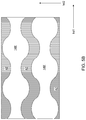
- FIG. 4B is a top-down view of the exemplary structure of FIG. 4A .
- the vertical plane A-A′ is the plane of the cross-section for FIG. 4A .
- FIG. 4C is a vertical cross-sectional view of the exemplary structure along the vertical plane C-C′ of FIG. 4B .
- FIG. 4D is a horizontal cross-sectional view of a region of the exemplary structure along the horizontal plane D-D′ of FIG. 4C .
- FIG. 5A is a vertical cross-sectional view of the exemplary structure after formation of pedestal channel rails according to an embodiment of the present disclosure.
- FIG. 5B is a horizontal cross-sectional view of the exemplary structure along the horizontal plane B-B′ of FIG. 5A .
- FIG. 6A is a vertical cross-sectional view of the exemplary structure after formation of a continuous memory film layer and a first continuous semiconductor channel material layer according to an embodiment of the present disclosure.
- FIG. 6B is a horizontal cross-sectional view of the exemplary structure along the horizontal plane B-B′ of FIG. 6A .
- FIG. 7A is a vertical cross-sectional view of the exemplary structure after anisotropic etch of the first continuous semiconductor channel material layer and the continuous memory film layer and deposition of a second continuous semiconductor channel material layer and a conformal dielectric material layer according to an embodiment of the present disclosure.
- FIG. 7B is a horizontal cross-sectional view of the exemplary structure along the horizontal plane B-B′ of FIG. 7A .
- FIG. 8A is a vertical cross-sectional view of the exemplary structure after isotropic etch back of the conformal dielectric material layer according to an embodiment of the present disclosure.
- FIG. 8B is a horizontal cross-sectional view of the exemplary structure along the horizontal plane B-B′ of FIG. 8A .
- FIG. 9A is a vertical cross-sectional view of the exemplary structure after isotropic etching of the second continuous semiconductor channel material layer and first semiconductor channel layers according to an embodiment of the present disclosure.
- FIG. 9B is a horizontal cross-sectional view of the exemplary structure along the horizontal plane B-B′ of FIG. 9A .
- FIG. 10A is a vertical cross-sectional view of the exemplary structure after formation of dielectric pillar structures according to an embodiment of the present disclosure.
- FIG. 10B is a horizontal cross-sectional view of the exemplary structure along the horizontal plane B-B′ of FIG. 10A .
- FIG. 11A is a vertical cross-sectional view of the exemplary structure after formation of drain regions according to an embodiment of the present disclosure.
- FIG. 11B is a top-down view of the exemplary structure of FIG. 11A .
- the hinged vertical plane A-A′ is the plane of the vertical cross-section of FIG. 11A .
- FIG. 11C is a vertical cross-sectional view of the exemplary structure along the vertical plane C-C′ of FIG. 11B .
- FIG. 11D is a horizontal cross-sectional view of the exemplary structure along the horizontal plane D-D′ of FIG. 11C .
- FIG. 12A is a vertical cross-sectional view of the exemplary structure after formation of via cavities according to an embodiment of the present disclosure.
- FIG. 12B is a top-down view of the exemplary structure of FIG. 12A .
- the hinged vertical plane A-A′ is the plane of the vertical cross-section of FIG. 12A .
- FIG. 12C is a vertical cross-sectional view of the exemplary structure along the vertical plane C-C′ of FIG. 12B .
- FIG. 13 is a vertical cross-sectional view of the exemplary structure after formation of backside recesses, conformal dielectric spacers, and planar dielectric portions according to an embodiment of the present disclosure.
- FIG. 14 is a vertical cross-sectional view of the exemplary structure after formation of electrically conductive strips according to an embodiment of the present disclosure.
- FIG. 15 is a vertical cross-sectional view of the exemplary structure after formation of source regions, insulating spacers, and source contact via structures according to an embodiment of the present disclosure.
- FIG. 16A is a vertical cross-sectional view of the exemplary structure after formation of additional contact via structures according to an embodiment of the present disclosure.
- FIG. 16B is a top-down view of the exemplary structure of FIG. 16A .
- the hinged vertical plane A-A′ is the plane of the vertical cross-section of FIG. 16A .
- FIG. 16C is a vertical cross-sectional view of the exemplary structure along the vertical plane C-C′ of FIG. 11B .
- FIG. 16D is a horizontal cross-sectional view of the exemplary structure along the horizontal plane D-D′ of FIG. 16C .
- FIG. 17 is a horizontal cross-sectional view of a configuration of the exemplary structure after formation of electrically conductive strips according to an embodiment of the present disclosure.
- the present disclosure is directed to a three-dimensional flat NAND memory device including wavy word lines and methods of manufacturing the same, the various aspects of which are described herein in detail.
- a first element located “on” a second element can be located on the exterior side of a surface of the second element or on the interior side of the second element.
- a first element is located “directly on” a second element if there exist a physical contact between a surface of the first element and a surface of the second element.
- a “layer” refers to a material portion including a region having a thickness.
- a layer may extend over the entirety of an underlying or overlying structure, or may have an extent less than the extent of an underlying or overlying structure. Further, a layer may be a region of a homogeneous or inhomogeneous continuous structure that has a thickness less than the thickness of the continuous structure. For example, a layer may be located between any pair of horizontal planes between, or at, a top surface and a bottom surface of the continuous structure. A layer may extend horizontally, vertically, and/or along a tapered surface.
- a substrate may be a layer, may include one or more layers therein, or may have one or more layer thereupon, thereabove, and/or therebelow.
- a monolithic three-dimensional memory array is one in which multiple memory levels are formed above a single substrate, such as a semiconductor wafer, with no intervening substrates.
- the term “monolithic” means that layers of each level of the array are directly deposited on the layers of each underlying level of the array.
- two dimensional arrays may be formed separately and then packaged together to form a non-monolithic memory device.
- non-monolithic stacked memories have been constructed by forming memory levels on separate substrates and vertically stacking the memory levels, as described in U.S. Pat. No.
- the substrates may be thinned or removed from the memory levels before bonding, but as the memory levels are initially formed over separate substrates, such memories are not true monolithic three-dimensional memory arrays.
- the various three-dimensional memory devices of the present disclosure include a monolithic three-dimensional NAND string memory device, and can be fabricated employing the various embodiments described herein.
- a semiconductor die, or a semiconductor package can include a memory chip.
- Each semiconductor package contains one or more dies (for example one, two, or four). The die is the smallest unit that can independently execute commands or report status.
- Each die contains one or more planes (typically one or two). Identical, concurrent operations can take place on each plane, although with some restrictions.
- Each plane contains a number of blocks, which are the smallest unit that can be erased by in a single erase operation.
- Each block contains a number of pages, which are the smallest unit that can be programmed, i.e., a smallest unit on which a read operation can be performed.
- the exemplary structure includes a substrate ( 9 , 10 ), which can be a semiconductor substrate.
- the substrate can include a substrate semiconductor layer 9 and an optional semiconductor material layer 10 .
- the substrate semiconductor layer 9 maybe a semiconductor wafer or a semiconductor material layer, and can include at least one elemental semiconductor material (e.g., single crystal silicon wafer or layer), at least one III-V compound semiconductor material, at least one II-VI compound semiconductor material, at least one organic semiconductor material, or other semiconductor materials known in the art.
- the substrate can have a major surface 7 , which can be, for example, a topmost surface of the substrate semiconductor layer 9 .
- the major surface 7 can be a semiconductor surface.
- the major surface 7 can be a single crystalline semiconductor surface, such as a single crystalline semiconductor surface.
- a “semiconducting material” refers to a material having electrical conductivity in the range from 1.0 ⁇ 10 ⁇ 6 S/cm to 1.0 ⁇ 10 5 S/cm.
- a “semiconductor material” refers to a material having electrical conductivity in the range from 1.0 ⁇ 10 ⁇ 6 S/cm to 1.0 ⁇ 10 5 S/cm in the absence of electrical dopants therein, and is capable of producing a doped material having electrical conductivity in a range from 1.0 S/cm to 1.0 ⁇ 10 5 S/cm upon suitable doping with an electrical dopant.
- an “electrical dopant” refers to a p-type dopant that adds a hole to a valence band within a band structure, or an n-type dopant that adds an electron to a conduction band within a band structure.
- a “conductive material” refers to a material having electrical conductivity greater than 1.0 ⁇ 10 5 S/cm.
- an “insulator material” or a “dielectric material” refers to a material having electrical conductivity less than 1.0 ⁇ 10 ⁇ 6 S/cm.
- a “heavily doped semiconductor material” refers to a semiconductor material that is doped with electrical dopant at a sufficiently high atomic concentration to become a conductive material either as formed as a crystalline material or if converted into a crystalline material through an anneal process (for example, from an initial amorphous state), i.e., to have electrical conductivity greater than 1.0 ⁇ 10 5 S/cm.
- a “doped semiconductor material” may be a heavily doped semiconductor material, or may be a semiconductor material that includes electrical dopants (i.e., p-type dopants and/or n-type dopants) at a concentration that provides electrical conductivity in the range from 1.0 ⁇ 10 ⁇ 6 S/cm to 1.0 ⁇ 10 5 S/cm.
- An “intrinsic semiconductor material” refers to a semiconductor material that is not doped with electrical dopants.
- a semiconductor material may be semiconducting or conductive, and may be an intrinsic semiconductor material or a doped semiconductor material.
- a doped semiconductor material can be semiconducting or conductive depending on the atomic concentration of electrical dopants therein.
- a “metallic material” refers to a conductive material including at least one metallic element therein. All measurements for electrical conductivities are made at the standard condition.
- At least one semiconductor device 700 for a peripheral circuitry can be formed on a portion of the substrate semiconductor layer 9 .
- the at least one semiconductor device can include, for example, field effect transistors.
- at least one shallow trench isolation structure 720 can be formed by etching portions of the substrate semiconductor layer 9 and depositing a dielectric material therein.
- a gate dielectric layer, at least one gate conductor layer, and a gate cap dielectric layer can be formed over the substrate semiconductor layer 9 , and can be subsequently patterned to form at least one gate structure ( 750 , 752 , 754 , 758 ), each of which can include a gate dielectric 750 , a gate electrode ( 752 , 754 ), and a gate cap dielectric 758 .
- the gate electrode ( 752 , 754 ) may include a stack of a first gate electrode portion 752 and a second gate electrode portion 754 .
- At least one gate spacer 756 can be formed around the at least one gate structure ( 750 , 752 , 754 , 758 ) by depositing and anisotropically etching a dielectric liner.
- Active regions 730 can be formed in upper portions of the substrate semiconductor layer 9 , for example, by introducing electrical dopants employing the at least one gate structure ( 750 , 752 , 754 , 758 ) as masking structures. Additional masks may be employed as needed.
- the active region 730 can include source regions and drain regions of field effect transistors.
- a first dielectric liner 761 and a second dielectric liner 762 can be optionally formed.
- Each of the first and second dielectric liners ( 761 , 762 ) can comprise a silicon oxide layer, a silicon nitride layer, and/or a dielectric metal oxide layer.
- silicon oxide includes silicon dioxide as well as non-stoichiometric silicon oxides having more or less than two oxygen atoms for each silicon atoms. Silicon dioxide is preferred.
- the first dielectric liner 761 can be a silicon oxide layer
- the second dielectric liner 762 can be a silicon nitride layer.
- the least one semiconductor device for the peripheral circuitry can contain a driver circuit for memory devices to be subsequently formed, which can include at least one NAND device.
- a dielectric material such as silicon oxide can be deposited over the at least one semiconductor device, and can be subsequently planarized to form a planarization dielectric layer 770 .
- the planarized top surface of the planarization dielectric layer 770 can be coplanar with a top surface of the dielectric liners ( 761 , 762 ).
- the planarization dielectric layer 770 and the dielectric liners ( 761 , 762 ) can be removed from an area to physically expose a top surface of the substrate semiconductor layer 9 .
- a surface is “physically exposed” if the surface is in physical contact with vacuum, or a gas phase material (such as air).
- the optional semiconductor material layer 10 can be formed on the top surface of the substrate semiconductor layer 9 prior to, or after, formation of the at least one semiconductor device 700 by deposition of a single crystalline semiconductor material, for example, by selective epitaxy.
- the deposited semiconductor material can be the same as, or can be different from, the semiconductor material of the substrate semiconductor layer 9 .
- the deposited semiconductor material can be any material that can be employed for the substrate semiconductor layer 9 as described above.
- the single crystalline semiconductor material of the semiconductor material layer 10 can be in epitaxial alignment with the single crystalline structure of the substrate semiconductor layer 9 .
- Portions of the deposited semiconductor material located above the top surface of the planarization dielectric layer 770 can be removed, for example, by chemical mechanical planarization (CMP).
- CMP chemical mechanical planarization
- the semiconductor material layer 10 can have a top surface that is coplanar with the top surface of the planarization dielectric layer 770 .
- the semiconductor material layer 10 can have a doping of a first conductivity type.
- the region (i.e., area) of the at least one semiconductor device 700 is herein referred to as a peripheral device region 200 .
- the region in which a memory array is subsequently formed is herein referred to as a memory array region 100 .
- a contact region 300 for subsequently forming stepped terraces of electrically conductive strips can be provided between the memory array region 100 and the peripheral device region 200 .
- a vertically alternating sequence of first material layers (such as insulating layers 32 L) and second material layers (such as spacer material layers) is formed over the substrate ( 9 , 10 ).
- a “vertically alternating sequence” refers to an alternating sequence of multiple instances of a first element and multiple instances of a second element that alternate vertically such that an instance of the second element overlies and/or underlies each instance of the first element, and an instance of the first element overlies and/or underlies each instance of the second element.
- the vertically alternating sequence can include a stack of an alternating plurality of first material layers (which can be insulating layers 32 L) and second material layers (which can be sacrificial material layer 42 L).
- a “material layer” refers to a layer including a material throughout the entirety thereof.
- an alternating plurality of first elements and second elements refers to a structure in which instances of the first elements and instances of the second elements alternate. Each instance of the first elements that is not an end element of the alternating plurality is adjoined by two instances of the second elements on both sides, and each instance of the second elements that is not an end element of the alternating plurality is adjoined by two instances of the first elements on both ends.
- a vertically alternating sequence of first elements and second elements is an alternating plurality of the first elements and the second elements in which the alternating of the first elements and second elements occurs along the vertical direction.
- the first elements may have the same thickness thereamongst, or may have different thicknesses.
- the second elements may have the same thickness thereamongst, or may have different thicknesses.
- the alternating plurality of first material layers and second material layers may begin with an instance of the first material layers or with an instance of the second material layers, and may end with an instance of the first material layers or with an instance of the second material layers.
- an instance of the first elements and an instance of the second elements may form a unit that is repeated with periodicity within the alternating plurality.
- Each first material layer includes a first material
- each second material layer includes a second material that is different from the first material.
- each first material layer can be an insulating layer 32 L
- each second material layer can be a sacrificial material layer.
- the stack can include an alternating plurality of insulating layers 32 L and sacrificial material layers 42 L, and constitutes a prototype stack of alternating layers comprising insulating layers 32 L and sacrificial material layers 42 L.
- a “prototype” structure or an “in-process” structure refers to a transient structure that is subsequently modified in the shape or composition of at least one component therein.
- the vertically alternating sequence ( 32 L, 42 L) can include insulating layers 32 L composed of the first material, and sacrificial material layers 42 L composed of a second material different from that of insulating layers 32 L.
- the first material of the insulating layers 32 L can be at least one insulating material.
- each insulating layer 32 L can be an insulating material layer.
- Insulating materials that can be employed for the insulating layers 32 L include, but are not limited to, silicon oxide (including doped or undoped silicate glass), silicon nitride, silicon oxynitride, organosilicate glass (OSG), spin-on dielectric materials, dielectric metal oxides that are commonly known as high dielectric constant (high-k) dielectric oxides (e.g., aluminum oxide, hafnium oxide, etc.) and silicates thereof, dielectric metal oxynitrides and silicates thereof, and organic insulating materials.
- the first material of the insulating layers 32 L can be silicon oxide.
- the second material of the sacrificial material layers 42 L is a sacrificial material that can be removed selective to the first material of the insulating layers 32 L.
- a removal of a first material is “selective to” a second material if the removal process removes the first material at a rate that is at least twice the rate of removal of the second material.
- the ratio of the rate of removal of the first material to the rate of removal of the second material is herein referred to as a “selectivity” of the removal process for the first material with respect to the second material.
- the sacrificial material layers 42 L may comprise an insulating material, a semiconductor material, or a conductive material.
- the second material of the sacrificial material layers 42 L can be subsequently replaced with electrically conductive electrodes which can function, for example, as control gate electrodes of a vertical NAND device.
- Non-limiting examples of the second material include silicon nitride, an amorphous semiconductor material (such as amorphous silicon), and a polycrystalline semiconductor material (such as polysilicon).
- the sacrificial material layers 42 L can be spacer material layers that comprise silicon nitride or a semiconductor material including at least one of silicon and germanium.
- the insulating layers 32 L can include silicon oxide, and sacrificial material layers can include silicon nitride sacrificial material layers.
- the first material of the insulating layers 32 L can be deposited, for example, by chemical vapor deposition (CVD).
- CVD chemical vapor deposition
- TEOS tetraethyl orthosilicate
- the second material of the sacrificial material layers 42 L can be formed, for example, CVD or atomic layer deposition (ALD).
- the sacrificial material layers 42 L can be suitably patterned so that conductive material portions to be subsequently formed by replacement of the sacrificial material layers 42 L can function as electrically conductive electrodes, such as the control gate electrodes of the monolithic three-dimensional NAND string memory devices to be subsequently formed.
- the sacrificial material layers 42 L may comprise a portion having a strip shape extending substantially parallel to the major surface 7 of the substrate.
- the thicknesses of the insulating layers 32 L and the sacrificial material layers 42 L can be in a range from 20 nm to 50 nm, although lesser and greater thicknesses can be employed for each insulating layer 32 L and for each sacrificial material layer 42 L.
- the number of repetitions of the pairs of an insulating layer 32 L and a sacrificial material layer (e.g., a control gate electrode or a sacrificial material layer) 42 L can be in a range from 2 to 1,024, and typically from 8 to 256, although a greater number of repetitions can also be employed.
- the top and bottom gate electrodes in the stack may function as the select gate electrodes.
- each sacrificial material layer 42 L in the vertically alternating sequence ( 32 L, 42 L) can have a uniform thickness that is substantially invariant within each respective sacrificial material layer 42 L.
- spacer material layers are sacrificial material layers 42 L that are subsequently replaced with electrically conductive strips
- embodiments are expressly contemplated herein in which the sacrificial material layers are formed as electrically conductive strips. In this case, steps for replacing the spacer material layers with electrically conductive strips can be omitted.
- an insulating cap layer 70 can be formed over the vertically alternating sequence ( 32 L, 42 L).
- the insulating cap layer 70 includes a dielectric material that is different from the material of the sacrificial material layers 42 L.
- the insulating cap layer 70 can include a dielectric material that can be employed for the insulating layers 32 L as described above.
- the insulating cap layer 70 can have a greater thickness than each of the insulating layers 32 L.
- the insulating cap layer 70 can be deposited, for example, by chemical vapor deposition.
- the insulating cap layer 70 can be a silicon oxide layer.
- the vertically alternating sequence of the insulating layers 32 L and the spacer material layers can be patterned to form stepped surfaces that continuously extend from a bottommost layer of the vertically alternating sequence ( 32 L, 42 L) to a topmost layer of the alternating sequence ( 32 L, 42 L) in the contact region 300 .
- a stepped cavity can be formed within the contact region 300 which is located between the memory array region 100 and the peripheral device region 200 containing the at least one semiconductor device for the peripheral circuitry.
- the stepped cavity can have various stepped surfaces such that the horizontal cross-sectional shape of the stepped cavity changes in steps as a function of the vertical distance from the top surface of the substrate ( 9 , 10 ).
- the stepped cavity can be formed by repetitively performing a set of processing steps.
- the set of processing steps can include, for example, an etch process of a first type that vertically increases the depth of a cavity by one or more levels, and an etch process of a second type that laterally expands the area to be vertically etched in a subsequent etch process of the first type.
- a “level” of a structure including alternating plurality is defined as the relative position of a pair of a first material layer and a second material layer within the structure.
- Stepped surfaces are formed at a peripheral portion of the vertically alternating sequence ( 32 L, 42 L) through formation of the stepped cavity.
- stepped surfaces refer to a set of surfaces that include at least two horizontal surfaces and at least two vertical surfaces such that each horizontal surface is adjoined to a first vertical surface that extends upward from a first edge of the horizontal surface, and is adjoined to a second vertical surface that extends downward from a second edge of the horizontal surface.
- a “stepped cavity” refers to a cavity having stepped surfaces.
- a terrace region is formed by patterning the vertically alternating sequence ( 32 L, 42 L).
- the terrace region includes stepped surfaces of the vertically alternating sequence ( 32 L, 42 L) that continuously extend from a bottommost layer within the vertically alternating sequence ( 32 L, 42 L) to a topmost layer within the vertically alternating sequence ( 32 L, 42 L).
- a retro-stepped dielectric material portion 65 (i.e., an insulating fill material portion) can be formed in the stepped cavity by deposition of a dielectric material therein.
- a dielectric material such as silicon oxide can be deposited in the stepped cavity. Excess portions of the deposited dielectric material can be removed from above the top surface of the insulating cap layer 70 , for example, by chemical mechanical planarization (CMP). The remaining portion of the deposited dielectric material filling the stepped cavity constitutes the retro-stepped dielectric material portion 65 .
- a “retro-stepped” element refers to an element that has stepped surfaces and a horizontal cross-sectional area that increases monotonically as a function of a vertical distance from a top surface of a substrate on which the element is present. If silicon oxide is employed for the retro-stepped dielectric material portion 65 , the silicon oxide of the retro-stepped dielectric material portion 65 may, or may not, be doped with dopants such as B, P, and/or F.
- a lithographic material stack (not shown) including at least a photoresist layer can be formed over the insulating cap layer 70 and the retro-stepped dielectric material portion 65 , and can be lithographically patterned to form width-modulated openings therein.
- a “width-modulated” element refers to an element in which the width of the element modulates along a lengthwise direction of the element, i.e., repeatedly increases and decreases along the lengthwise direction of the element.
- the width-modulated openings laterally extend along a first horizontal direction hd 1 , and have a width modulation along a second horizontal direction hd 2 that is perpendicular to the first horizontal direction hd 1 .
- the pattern in the lithographic material stack can be transferred through the insulating cap layer 70 or the retro-stepped dielectric material portion 65 , and through the vertically alternating sequence ( 32 L, 42 L) by at least one anisotropic etch that employs the patterned lithographic material stack as an etch mask. Portions of the vertically alternating sequence ( 32 L, 42 L) underlying the width-modulated openings in the patterned lithographic material stack are etched to form width-modulated line trenches 149 .
- a “line trench” refers to a trench that generally extends laterally along a horizontal direction.
- the width-modulated line trenches 149 are formed through the vertically alternating sequence ( 32 L, 42 L). Each patterned portion of the insulating layers 32 L that generally extend along the first horizontal direction hd 1 and having lateral undulations in the sidewalls along the second horizontal direction hd 2 constitutes an insulating strip 32 . Each patterned portion of the sacrificial material layers 42 L that generally extend along the second horizontal direction hd 2 and having lateral undulations in the sidewalls along the first horizontal direction hd 2 constitutes a sacrificial material strip 42 . The width-modulated line trenches 149 laterally extend along the first horizontal direction hd 1 and are laterally spaced apart along the second horizontal direction hd 2 . Remaining portions of the vertically alternating stack ( 32 L, 42 L) include alternating stacks of insulating strips 32 and sacrificial material strips 42 are formed by remaining portions of the vertically alternating sequence ( 32 L, 42 L).
- Each of the width-modulated line trenches 149 can be formed with a pair of sidewalls that generally extend along the first horizontal direction (e.g., word line direction) hd 1 and having a lateral undulation along the second horizontal direction (e.g., bit line direction) hd 2 .
- each of the pair of sidewalls can include a laterally alternating sequence of laterally-concave and laterally-convex and vertically-planar sidewall segments.
- each paid of sidewalls can also include vertically-planar sidewall segments between laterally-concave and laterally-convex sidewall segments.
- a laterally-concave sidewall refers to a sidewall having a concave horizontal cross-sectional profile.
- a laterally-convex sidewall refers to a sidewall having a convex horizontal cross-sectional profile.
- a vertically-planar sidewall refers to a sidewall having a vertically-extending straight line as a vertical cross-sectional profile.
- each of the width-modulated line trenches 149 includes a periodic laterally alternating sequence of a neck region 149 N and a bulbous region 149 B.
- a neck region 149 N refers to a region having a lesser width, W 1 , than neighboring regions
- a bulbous region 149 B refers to a region having a greater width W 2 than neighboring regions.
- neck regions 149 N of a first width-modulated line trench 149 P within each neighboring pair of the width-modulated line trenches 149 is laterally offset along the first horizontal direction hd 1 from a neck region 149 N of a second width-modulated line trench 149 Q within each neighboring pair of the width-modulated line trenches 149 by a lateral offset distance that is one half of a periodicity p of neck regions of the first width-modulated line trench 149 along the first horizontal direction hd 1 .
- the minimum width W 1 of the neck regions 149 N in the second horizontal direction is less than the maximum width of the bulbous the neck regions 149 N and the bulbous regions 149 B in two neighboring width-modulated line trenches 149 can be arranged such that the alternating stack ( 32 , 42 ) of insulating strips 32 and sacrificial material strips 42 there between has a substantially uniform width W 3 or a width variation less than 50%, and/or less than 25%, and/or less than 10%, and/or less than 5% of the average width W 3 of the alternating stack ( 32 , 42 ).
- the average width W 3 of the alternating stack ( 32 , 42 ) in the second horizontal direction hd 2 remains substantially at any location along the first horizontal direction hd 1 .
- the width-modulated line trenches 149 laterally extend through the entire memory array region 100 , and may laterally extend at least partly into the contact region 300 .
- the width-modulated line trenches 149 may laterally extend through the entire contact region 300 along the first horizontal direction hd 1 , or may laterally extend only through part of a width, but not the entire width along the first horizontal direction hd 1 , of the contact region 300 .
- an overetch into the semiconductor material layer 10 may be optionally performed after the top surface of the semiconductor material layer 10 is physically exposed at a bottom of each width-modulated line trench 149 . The overetch may be performed prior to, or after, removal of the lithographic material stack.
- the recessed surfaces of the semiconductor material layer 10 may be vertically offset from the un-recessed top surfaces of the semiconductor material layer 10 by a recess depth.
- the recess depth can be, for example, in a range from 1 nm to 50 nm, although lesser and greater recess depths can also be employed.
- the overetch is optional, and may be omitted. If the overetch is not performed, the bottom surfaces of the width-modulated line trenches 149 can be coplanar with the topmost surface of the semiconductor material layer 10 .
- Each of the width-modulated line trenches 149 may include a sidewall (or a plurality of sidewalls) that extends substantially perpendicular to the topmost surface of the substrate.
- the substrate semiconductor layer 9 and the semiconductor material layer 10 collectively constitute a substrate ( 9 , 10 ), which can be a semiconductor substrate.
- the semiconductor material layer 10 may be omitted, and the width-modulated line trenches 149 can be extend to a top surface of the substrate semiconductor layer 9 .
- the insulating strips 32 and the sacrificial material strips 42 may be interconnected among one another by a connecting portion provided within the contact region 300 , and the insulating strips 32 may be portions of a continuous insulating layer that extend across the memory array region 100 and the contact region 300 .
- a plurality of alternating stacks of insulating strips 32 and sacrificial material strips 42 may be interconnected among one another by connecting portions within the contact region 300 .
- the insulating strips 32 and the sacrificial material strips 42 may be divided into discrete material strips by the width-modulated line trenches 149 .
- width-modulated line trenches 149 in the memory array region 100 are illustrated.
- the width-modulated line trenches 149 extends through the insulating cap layer 70 , the alternating stacks ( 32 , 42 ), and optionally into an upper portion of the semiconductor material layer 10 .
- the recess depth of the bottom surface of each memory opening with respect to the top surface of the semiconductor material layer 10 can be in a range from 0 nm to 30 nm, although greater recess depths can also be employed.
- the sacrificial material strips 42 can be laterally recessed partially to form lateral recesses (not shown), for example, by an isotropic etch.
- An optional pedestal channel rail 11 R can be formed at the bottom portion of each width-modulated line trench 149 by a selective semiconductor material deposition process such as selective epitaxy.
- the selective semiconductor material deposition process employs concurrent or alternating flow of a semiconductor precursor and an etchant. Semiconductor surfaces provide a higher deposition rate than insulating surface. By selecting the etch rate of the etchant between the deposition rate of the semiconductor material on semiconductor surfaces and the deposition rate of the semiconductor material on insulating surfaces, the semiconductor material can grow only from physically exposed surfaces during the selective semiconductor material deposition process.
- the pedestal channel rail 11 R can be doped with electrical dopants of the same conductivity type as the semiconductor material layer 10 .
- each pedestal channel rail 11 R can be formed above a horizontal plane including the top surfaces of bottommost sacrificial material strips 42 .
- at least one source select gate electrode can be subsequently formed by replacing the bottommost sacrificial material strip 42 located below the horizontal plane including the top surfaces of the pedestal channel rails 11 R with electrically conductive strips.
- the pedestal channel rail 11 R can be a portion of a transistor channel that extends between a source region to be subsequently formed in the substrate ( 9 , 10 ) and a drain region to be subsequently formed in an upper portion of the width-modulated line trench 149 .
- a width-modulated line cavity 149 ′ is present in the unfilled portion of the width-modulated line trench 149 above the pedestal channel rail 11 R.
- the pedestal channel rail 11 R can comprise single crystalline silicon.
- the pedestal channel rail 11 R can have a doping of the first conductivity type, which is the same as the conductivity type of the semiconductor material layer 10 that the pedestal channel rail contacts. If a semiconductor material layer 10 is not present, the pedestal channel rail 11 R can be formed directly on the substrate semiconductor layer 9 , which can have a doping of the first conductivity type.
- a continuous memory film layer 50 L is formed in the width-modulated line trenches 149 .
- the continuous memory film layer 50 L includes a stack of layers including a continuous blocking dielectric layer 52 L, a continuous charge storage layer 54 L, and a continuous tunneling dielectric layer 56 L.
- the continuous blocking dielectric layer 52 L can include a single dielectric material layer or a stack of a plurality of dielectric material layers.
- the continuous blocking dielectric layer can include a dielectric metal oxide layer consisting essentially of a dielectric metal oxide.
- a dielectric metal oxide refers to a dielectric material that includes at least one metallic element and at least oxygen.
- the dielectric metal oxide may consist essentially of the at least one metallic element and oxygen, or may consist essentially of the at least one metallic element, oxygen, and at least one non-metallic element such as nitrogen.
- the continuous blocking dielectric layer 52 L can include a dielectric metal oxide having a dielectric constant greater than 7.9, i.e., having a dielectric constant greater than the dielectric constant of silicon nitride.
- Non-limiting examples of dielectric metal oxides include aluminum oxide (Al 2 O 3 ), hafnium oxide (HfO 2 ), lanthanum oxide (LaO 2 ), yttrium oxide (Y 2 O 3 ), tantalum oxide (Ta 2 O 5 ), silicates thereof, nitrogen-doped compounds thereof, alloys thereof, and stacks thereof.
- the dielectric metal oxide layer can be deposited, for example, by chemical vapor deposition (CVD), atomic layer deposition (ALD), pulsed laser deposition (PLD), liquid source misted chemical deposition, or a combination thereof.
- the thickness of the dielectric metal oxide layer can be in a range from 1 nm to 20 nm, although lesser and greater thicknesses can also be employed.
- the dielectric metal oxide layer can subsequently function as a dielectric material portion that blocks leakage of stored electrical charges to control gate electrodes.
- the continuous blocking dielectric layer 52 L includes aluminum oxide.
- the continuous blocking dielectric layer 52 L can include multiple dielectric metal oxide layers having different material compositions.
- the continuous blocking dielectric layer 52 L can include a dielectric semiconductor compound such as silicon oxide, silicon oxynitride, silicon nitride, or a combination thereof.
- the continuous blocking dielectric layer 52 L can include silicon oxide.
- the dielectric semiconductor compound of the continuous blocking dielectric layer 52 L can be formed by a conformal deposition method such as low pressure chemical vapor deposition, atomic layer deposition, or a combination thereof.
- the thickness of the dielectric semiconductor compound can be in a range from 1 nm to 20 nm, although lesser and greater thicknesses can also be employed.
- the continuous blocking dielectric layer 52 L can be omitted, and a backside continuous blocking dielectric layer can be formed after formation of backside recesses on surfaces of memory films to be subsequently formed.
- the continuous charge storage layer 54 L can be formed.
- the continuous charge storage layer 54 L can be a continuous layer or patterned discrete portions of a charge trapping material including a dielectric charge trapping material, which can be, for example, silicon nitride.
- the continuous charge storage layer 54 L can include a continuous layer or patterned discrete portions of a conductive material such as doped polysilicon or a metallic material that is patterned into multiple electrically isolated portions (e.g., floating gates), for example, by being formed within lateral recesses into sacrificial material strips 42 .
- the continuous charge storage layer 54 L includes a silicon nitride layer.
- the sacrificial material strips 42 and the insulating strips 32 can have vertically coincident sidewalls, and the continuous charge storage layer 54 L can be formed as a single continuous layer.
- the sacrificial material strips 42 can be laterally recessed with respect to the sidewalls of the insulating strips 32 , and a combination of a deposition process and an anisotropic etch process can be employed to form the continuous charge storage layer 54 L as a plurality of memory material portions that are vertically spaced apart. While the present disclosure is described employing an embodiment in which the continuous charge storage layer 54 L is a single continuous layer, embodiments are expressly contemplated herein in which the continuous charge storage layer 54 L is replaced with a plurality of memory material portions (which can be charge trapping material portions or electrically isolated conductive material portions) that are vertically spaced apart.
- the continuous charge storage layer 54 L can be formed as a single continuous charge storage layer of homogeneous composition, or can include a stack of multiple continuous charge storage layers.
- the multiple continuous charge storage layers can comprise a plurality of spaced-apart floating gate material layers that contain conductive materials (e.g., metal such as tungsten, molybdenum, tantalum, titanium, platinum, ruthenium, and alloys thereof, or a metal silicide such as tungsten silicide, molybdenum silicide, tantalum silicide, titanium silicide, nickel silicide, cobalt silicide, or a combination thereof) and/or semiconductor materials (e.g., polycrystalline or amorphous semiconductor material including at least one elemental semiconductor element or at least one compound semiconductor material).
- conductive materials e.g., metal such as tungsten, molybdenum, tantalum, titanium, platinum, ruthenium, and alloys thereof, or a metal silicide such as tungsten silicide, mo
- the continuous charge storage layer 54 L may comprise an insulating charge trapping material, such as one or more silicon nitride segments.
- the continuous charge storage layer 54 L may comprise conductive nanoparticles such as metal nanoparticles, which can be, for example, ruthenium nanoparticles.
- the continuous charge storage layer 54 L can be formed, for example, by chemical vapor deposition (CVD), atomic layer deposition (ALD), physical vapor deposition (PVD), or any suitable deposition technique for storing electrical charges therein.
- the thickness of the continuous charge storage layer 54 L can be in a range from 2 nm to 20 nm, although lesser and greater thicknesses can also be employed.
- the continuous tunneling dielectric layer 56 L includes a dielectric material through which charge tunneling can be performed under suitable electrical bias conditions.
- the charge tunneling may be performed through hot-carrier injection or by Fowler-Nordheim tunneling induced charge transfer depending on the mode of operation of the monolithic three-dimensional NAND string memory device to be formed.
- the continuous tunneling dielectric layer 56 L can include silicon oxide, silicon nitride, silicon oxynitride, dielectric metal oxides (such as aluminum oxide and hafnium oxide), dielectric metal oxynitride, dielectric metal silicates, alloys thereof, and/or combinations thereof.
- the continuous tunneling dielectric layer 56 L can include a stack of a first silicon oxide layer, a silicon oxynitride layer, and a second silicon oxide layer, which is commonly known as an ONO stack.
- the continuous tunneling dielectric layer 56 L can include a silicon oxide layer that is substantially free of carbon or a silicon oxynitride layer that is substantially free of carbon.
- the thickness of the continuous tunneling dielectric layer 56 L can be in a range from 2 nm to 20 nm, although lesser and greater thicknesses can also be employed.
- An optional first continuous semiconductor channel material layer 601 L can be deposited on the continuous memory film layer 50 L.
- the optional first continuous semiconductor channel material layer 601 L includes a semiconductor material such as at least one elemental semiconductor material, at least one III-V compound semiconductor material, at least one II-VI compound semiconductor material, at least one organic semiconductor material, or other semiconductor materials known in the art.
- the first continuous semiconductor channel material layer 601 L includes amorphous silicon or polysilicon.
- the first continuous semiconductor channel material layer 601 L can be formed by a conformal deposition method such as low pressure chemical vapor deposition (LPCVD).
- the thickness of the first continuous semiconductor channel material layer 601 L can be in a range from 2 nm to 10 nm, although lesser and greater thicknesses can also be employed.
- a width-modulated line cavity 149 ′ is formed in the volume of each width-modulated line trench 149 that is not filled with the deposited material layers ( 52 L, 54 L, 56 L, 601 L).
- the continuous memory film layer 50 L is formed on the sidewalls of the alternating stacks ( 32 , 42 ) in the width-modulated line trenches 149 .
- the continuous memory film layer 50 L includes a continuous blocking dielectric layer 52 L that contacts a respective one of the alternating stacks ( 32 , 42 ), a continuous charge storage layer 54 L contacting the continuous blocking dielectric layer 52 L, and a continuous tunneling dielectric layer 56 L contacting the continuous charge storage layer 541 and the first continuous semiconductor channel material layer 601 L.
- horizontal portions of the optional first continuous semiconductor channel material layer 601 L, the continuous tunneling dielectric layer 56 L, the continuous charge storage layer 54 L, and the continuous blocking dielectric layer 52 L are sequentially anisotropically etched employing at least one anisotropic etch process.
- the etch chemistry of the at least one anisotropic etch process can be sequentially changed to etch horizontal portions of the various material layers.
- Each remaining portion of the optional first continuous semiconductor channel material layer 601 L constitutes a first vertical semiconductor channel portion 601 .
- Each remaining portion of the continuous tunneling dielectric layer 56 L constitutes a tunneling dielectric 56 .
- Each remaining portion of the continuous charge storage layer 54 L constitutes a charge storage layer 54 .
- Each remaining portion of the continuous blocking dielectric layer 52 L constitutes a blocking dielectric 52 .
- Each of the first vertical semiconductor channel portions 601 , the tunneling dielectrics 56 , the charge storage layers 54 , and the blocking dielectrics 52 can have a tubular configuration, and can be topologically homeomorphic to a torus.
- an element is topologically homeomorphic to a torus if the shape of the element can be continuously stretched without destroying a hole or forming a new hole into the shape of a torus.
- Each contiguous combination of a tunneling dielectric 56 , a charge storage layer 54 , and a blocking dielectric 52 constitutes a memory film 50 .
- a surface of a pedestal channel rail 11 R (or a surface of the semiconductor material layer 10 in case the pedestal channel rails 11 R are not employed) can be physically exposed underneath each opening through a stack of a memory film 50 and a first vertical semiconductor channel portion 601 .
- the physically exposed semiconductor surface at the bottom of each width-modulated line cavity 149 ′ can be vertically recessed so that the recessed semiconductor surface underneath each width-modulated line cavity 149 ′ is vertically offset from the topmost surfaces of the pedestal channel rails 11 R (or of the semiconductor material layer 10 in case pedestal channel rails 11 R are not employed) by a recess distance.
- a second continuous semiconductor channel material layer 602 L can be deposited directly on the semiconductor surface of the pedestal channel rail 11 R (or the semiconductor material layer 10 if the pedestal channel rail 11 R is omitted), and directly on the first vertical semiconductor channel portions 601 .
- the second continuous semiconductor channel material layer 602 L includes a semiconductor material such as at least one elemental semiconductor material, at least one III-V compound semiconductor material, at least one II-VI compound semiconductor material, at least one organic semiconductor material, or other semiconductor materials known in the art.
- the second continuous semiconductor channel material layer 602 L includes amorphous silicon or polysilicon.
- the second continuous semiconductor channel material layer 602 L can be formed by a conformal deposition method such as low pressure chemical vapor deposition (LPCVD).
- the thickness of the second continuous semiconductor channel material layer 602 L can be in a range from 2 nm to 10 nm, although lesser and greater thicknesses can also be employed.
- the second continuous semiconductor channel material layer 602 L partially fills the width-modulated line cavity 149 ′ in each width-modulated line trench 149 .
- the materials of the first vertical semiconductor channel portions 601 and the second continuous semiconductor channel material layer 602 L are collectively referred to as a semiconductor channel material.
- the semiconductor channel material is a set of all semiconductor materials in the first vertical semiconductor channel portions 601 and the second continuous semiconductor channel material layer 602 L.
- a conformal dielectric material layer 62 L is formed on the second continuous semiconductor channel material layer 602 L.
- the conformal dielectric material layer 62 L includes a dielectric material that can be isotropically etched selective to the material of the second continuous semiconductor channel material layer 602 L.
- the conformal dielectric material layer 62 L can include doped silicate glass, undoped silicate glass, or organosilicate glass.
- the neck regions 149 N of the width-modulated line trenches 149 are filled with the material of the conformal dielectric material layer 62 L, while the bulbous regions 149 B of the width-modulated line trenches 149 are not completely filled by the material of the conformal dielectric material layer 62 L. Pillar cavities 49 ′ that are not filled with the conformal dielectric material layer 62 L are present in the bulbous regions 149 B, while the conformal dielectric material layer 62 L completely fills the neck regions 149 N.
- a first etch process is performed, which etches back the material of the conformal dielectric material layer 62 L.
- a chemical dry etch process can be used to recess the conformal dielectric material layer 62 L.
- the duration of the first etch process is selected such that the etch distance is in a range from 100% to 140%, such as from 100% to 120%, of the thickness of the conformal dielectric material layer 62 L.
- Portions of the conformal dielectric material layer 62 L in the bulbous regions 149 B are removed without removing portions of the conformal dielectric material layer 62 L in the neck regions 149 N.
- Horizontal portions of the conformal dielectric material layer 62 L are removed from above the insulating cap layer 70 and at the bottom of each pillar cavity 49 ′. Remaining portions of the conformal dielectric material layer 62 L in the neck regions constitute dielectric cores 62 after the etch process.
- the pillar cavities 49 ′ are laterally expanded by the etch process to physically expose surface portions of the second continuous semiconductor channel material layer 602 L in the bulbous regions 149 B.
- a second etch process is performed, which etches the semiconductor channel material of the second continuous semiconductor channel material layer 602 L and the first vertical semiconductor channel portions 601 selective to the material of the dielectric cores 62 .
- the exposed semiconductor channel material in the bulbous regions 149 B is removed, while the semiconductor channel material that is protected by the dielectric 62 cores in the neck regions 149 N is not removed.
- the chemistry of the second etch process can be selective to the materials of the memory films 50 .
- the second etch process can include a wet etch process employing hot trimethyl-2 hydroxyethyl ammonium hydroxide (“hot TMY”) or tetramethyl ammonium hydroxide (TMAH).
- the duration of the second etch process can be selected such that the etch distance through the semiconductor channel material is at least the sum of the thickness of the second continuous semiconductor channel material layer 602 L and the thickness of a first vertical semiconductor channel portion 601 .
- the etch distance through the semiconductor channel material is in a range from 100% to 140%, such as from 100% to 120%, of the sum of the thickness of the second continuous semiconductor channel material layer 602 L and the thickness of a first vertical semiconductor channel portion 601 .
- the portions of the second continuous semiconductor channel material layer 602 L and the first vertical semiconductor channel portions 601 that are not masked by the dielectric cores 62 in the bulbous regions 149 B are removed by the second etch process. Each remaining portion of the second continuous semiconductor channel material layer 602 L constitutes a second vertical semiconductor channel portion 602 . Each remaining contiguous set of a second vertical semiconductor channel portion 602 and a first vertical semiconductor channel portion 601 constitutes a vertical semiconductor channel 60 .
- Each of the vertical semiconductor channels 60 includes a respective laterally-concave and vertically-planar outer sidewall that is formed directly on a laterally-convex and vertically-planar sidewall of a respective one of the memory films 50 .
- Each of the vertical semiconductor channels 60 can be located in one of the neck regions of the width-modulated line trenches 149 .
- the memory films 50 can remain on a respective sidewall of the alternating stacks ( 32 , 42 ) in both the bulbous regions 149 B and the neck regions 149 N. Thus, the memory films 50 are continuous throughout the entire width-modulated line trenches 149 , while the semiconductor channels 60 remain only in the neck regions 149 N. Each of the memory films 50 generally extends along the first horizontal direction hd 1 , and laterally undulates along the second horizontal direction hd 2 .
- Each of the memory films 50 includes a respective layer stack ( 52 , 54 , 56 ) that comprises a blocking dielectric 52 that contacts a respective one of the alternating stacks ( 32 , 42 ), a charge storage layer 54 contacting the blocking dielectric 52 , and a tunneling dielectric 56 contacting the charge storage layer 54 .
- a row of discrete vertical semiconductor channels 60 is located within the neck regions 149 N of a respective width-modulated line trench 149 .
- dielectric pillar structures 162 are formed in the pillar cavities 49 ′.
- a dielectric material can be formed in the pillar cavities 49 ′ after forming the vertical semiconductor channels 60 by deposition and planarization of the dielectric material.
- the dielectric material can include, for example, undoped silicate glass, doped silicate glass, or organosilicate glass. Excess portions of the dielectric material can be removed from above the horizontal plane including the top surfaces of the insulating cap layer 70 by a recess etch.
- the dielectric pillar structures 162 can be formed as a two-dimensional array of dielectric pillar structures 162 that are located within the bulbous regions of the width-modulated line trenches 149 .
- each of the dielectric pillar structures 162 includes a pair of first laterally-convex and vertically-planar sidewalls that contact a respective pair of memory films 50 .
- each of the dielectric pillar structures 162 includes a pair of second laterally-convex and vertically-planar sidewalls that contact a respective pair of dielectric cores 62 .
- each of the width-modulated line trenches 149 includes a laterally alternating sequence of dielectric cores 62 and dielectric pillar structures 162 , and each interface between a neighboring pair of a dielectric core 62 and a dielectric pillar structure 162 includes a surface at which a laterally convex-sidewall of the dielectric pillar structure 162 contacts a laterally-concave sidewall of the dielectric core 62 .
- the dielectric pillar structure 162 and memory films 50 remain in the bulbous regions 149 B, while the semiconductor channels 60 , the memory films 50 and the dielectric cores remain in the neck regions 149 N.
- the dielectric cores 62 can be vertically recessed without recessing at least a center region of each dielectric pillar structure 162 .
- a photoresist layer can be applied over the exemplary structure and can be lithographically patterned to provide openings in areas of the dielectric cores 62 and optionally in areas around the dielectric cores 62 .
- the dielectric cores 62 can be vertically recessed through openings in the photoresist layer by an anisotropic etch process.
- the depth of the recess can be selected such that the recessed surfaces of the dielectric cores 62 are located between a horizontal plane including the top surfaces of the insulating cap layer 70 and a horizontal plane including the bottom surfaces of the insulating cap layer 70 .
- the photoresist layer can be subsequently removed, for example, by ashing.
- a doped semiconductor material having a doping of a second conductivity type is formed in the recessed regions between neighboring pairs of vertical semiconductor channels 60 .
- the second conductivity type is the opposite of the first conductivity type.
- the doped semiconductor material can include electrical dopants of the second conductivity type (e.g., n-type) at an atomic concentration in a range from 5.0 ⁇ 10 19 /cm 3 to 1.0 ⁇ 10 21 /cm 3 .
- the dopants can be provided in-situ during deposition and/or by ion implantation after deposition of the semiconductor material.
- Portions of the deposited doped semiconductor material of the second conductivity type that overlie the horizontal plane including the top surfaces of the patterned portions of the insulating cap layer 70 can be removed by a planarization process, which can be a recess etch that etches the semiconductor materials selective to the dielectric material of the insulating cap layer 70 or a chemical mechanical planarization (CMP) process.
- a planarization process which can be a recess etch that etches the semiconductor materials selective to the dielectric material of the insulating cap layer 70 or a chemical mechanical planarization (CMP) process.
- Each remaining portion of the doped semiconductor material of the second conductivity type constitutes a drain region 63 .
- the structures located within the neck regions 149 N of the width-modulated line trenches 149 are herein referred to as a memory opening fill structure 58 .
- Each memory opening fill structure 58 includes a portion of an optional pedestal channel rail 11 R, a pair of memory films 50 , a pair of vertical semiconductor channels
- backside via cavities 69 and/or elongated backside trenches 169 are formed.
- the backside via cavities 69 can be formed in discrete locations that intersect the width-modulated line trenches 149 while the elongated backside trenches 169 are formed through portions of the line trenches 149 located in the contact region 300 .
- a photoresist layer can be applied over the exemplary structure, and can be lithographically patterned to form openings in at least one of areas of a subset of the dielectric pillar structures 162 within the memory array region 100 and/or in areas corresponding to lateral extensions of the width-modulated line trenches 149 into the contact region 300 .
- An anisotropic etch is performed through the level of the insulating cap layer 70 and through each level of the sacrificial material strips 42 .
- the anisotropic etch can form cavities ( 69 , 169 ) that extend through the entire thickness of the alternating stacks ( 32 , 42 ).
- the backside via cavities 69 are formed in the memory array region 100 in, and around, the areas of the subset of the dielectric pillar structures 162 .
- the elongated backside trenches 169 are formed in the contact region 300 in, and around, the areas that correspond to the extensions of the width-modulated line trenches 149 into the contact region 300 .
- the elongated backside trenches 169 may have straight sidewalls that laterally extend along the first horizontal direction hd 1 .
- the backside via cavities 69 can have substantially vertical sidewalls, and extend through the subset of the dielectric pillar structures 162 and through portions of the memory films 50 .
- the subset of the dielectric pillar structures 162 may be partially or completely removed upon formation of the backside via cavities 69 .
- Portions of the pedestal channel rails 11 R that underlie the subset of the dielectric pillar structures 162 can be removed.
- Portions of the memory films 50 exposed in the backside via cavities 69 can be removed to physically exposed sidewalls of the alternating stacks ( 32 , 42 ). Sidewalls of the sacrificial material strips 42 of a neighboring pair of alternating stacks ( 32 , 42 ) that are physically exposed backside via cavities 69 .
- the bottom surfaces of the backside via cavities 69 can be at, or below, the horizontal plane including the bottommost surfaces of the sacrificial material strips 42 in each backside via cavity 69 .
- the backside via cavities 69 can be formed at regular intervals along the first horizontal direction hd 1 for each of the line trenches 149 .
- the elongated backside trenches 169 laterally extend along the first horizontal direction hd 1 in the contact region 300 .
- the width-modulated line trenches 149 do not completely divide the vertically alternating sequence of the insulating layers 32 L and the sacrificial material layers 42 L into discrete alternating stacks ( 32 , 42 ) of insulating strips 32 and sacrificial material strips 42 at the processing steps of FIGS.
- the elongated backside trenches 169 may divide the vertically alternating sequence of the insulating layers 32 L and the sacrificial material layers 42 L into discrete alternating stacks ( 32 , 42 ) of insulating strips 32 and sacrificial material strips 42 at this processing step. Sidewalls of the sacrificial material strips 42 within a neighboring pair of alternating stacks ( 32 , 42 ) are physically exposed at each level of the sacrificial material strips 42 around each elongated backside trench 169 .
- the bottom surfaces of the elongated backside trenches 169 can be at, or below, the horizontal plane including the bottommost surfaces of the sacrificial material strips 42 .
- the width-modulated line trenches 149 can be modified by the backside via cavities 69 and the elongated backside trenches 169 .
- the widths of the backside via cavities 69 and the elongated backside trenches 169 can be greater than the maximum width of the width-modulated line trenches 149 prior to formation of the backside via cavities 69 and the elongated backside trenches 169 to ensure that sidewalls of the sacrificial material strips 42 are physically exposed on both sides of each of the backside via cavities 69 and the elongated backside trenches 169 .
- an etchant that selectively etches the second material of the sacrificial material strips 42 with respect to the first material of the insulating strips 32 can be introduced into the backside via cavities 69 and the elongated backside trenches 169 , for example, employing an etch process.
- Backside recesses 43 are formed in volumes from which the sacrificial material strips 42 are removed.
- the removal of the second material of the sacrificial material strips 42 can be selective to the first material of the insulating strips 32 , the material of the retro-stepped dielectric material portion 65 , the semiconductor material of the semiconductor material layer 10 , and the material of the outermost layer of the memory films 50 .
- the sacrificial material strips 42 can include silicon nitride, and the materials of the insulating strips 32 and the retro-stepped dielectric material portion 65 can be selected from silicon oxide and dielectric metal oxides.
- the etch process that removes the second material selective to the first material and the outermost layer of the memory films 50 can be a wet etch process employing a wet etch solution, or can be a gas phase (dry) etch process in which the etchant is introduced in a vapor phase into the backside via cavities 69 and the elongated backside trenches 169 .
- the etch process can be a wet etch process in which the exemplary structure is immersed within a wet etch tank including phosphoric acid, which etches silicon nitride selective to silicon oxide, silicon, and various other materials employed in the art.
- Each backside recess 43 can be a laterally undulating cavity having a lateral dimension that is greater than the vertical extent of the cavity along the first horizontal direction hd 1 . In other words, the lateral dimension of each backside recess 43 along the first horizontal direction hd 1 can be greater than the height of the backside recess 43 .
- a plurality of backside recesses 43 can be formed in the volumes from which the second material of the sacrificial material strips 42 is removed.
- the memory array region 100 comprises an array of monolithic three-dimensional NAND strings having a plurality of device levels disposed above the substrate ( 9 , 10 ). In this case, each backside recess 43 can define a space for receiving a respective word line of the array of monolithic three-dimensional NAND strings.
- Each of the plurality of backside recesses 43 can extend substantially parallel to the top surface of the substrate ( 9 , 10 ).
- a backside recess 43 can be vertically bounded by a top surface of an underlying insulating strip 32 and a bottom surface of an overlying insulating strip 32 .
- each backside recess 43 can have a uniform height throughout.
- Physically exposed surface portions of the optional pedestal channel rails 11 R and the semiconductor material layer 10 can be converted into dielectric material portions by thermal conversion and/or plasma conversion of the semiconductor materials into dielectric materials.
- thermal conversion and/or plasma conversion can be employed to convert a surface portion of each pedestal channel rail 11 R into a conformal dielectric spacer 116 , and to convert each physically exposed surface portion of the semiconductor material layer 10 into a planar dielectric portion 616 .
- the conformal dielectric spacers 116 include a dielectric material that includes the same semiconductor element as the pedestal channel rails 11 R and additionally includes at least one non-metallic element such as oxygen and/or nitrogen such that the material of the conformal dielectric spacers 116 is a dielectric material.
- the conformal dielectric spacers 116 can include a dielectric oxide, a dielectric nitride, or a dielectric oxynitride of the semiconductor material of the pedestal channel rails 11 R.
- each planar dielectric portion 616 includes a dielectric material that includes the same semiconductor element as the semiconductor material layer and additionally includes at least one non-metallic element such as oxygen and/or nitrogen such that the material of the planar dielectric portions 616 is a dielectric material.
- the planar dielectric portions 616 can include a dielectric oxide, a dielectric nitride, or a dielectric oxynitride of the semiconductor material of the semiconductor material layer 10 .
- a backside blocking dielectric layer 44 can be subsequently formed in the backside recesses 43 .
- the backside blocking dielectric layer 44 can include at least one dielectric material that is subsequently employed to prevent charge tunneling between the charge storage layers 54 and electrically conductive strips to be subsequently formed in the backside recesses 43 .
- the backside blocking dielectric layer 44 can include silicon oxide and/or a dielectric metal oxide such as aluminum oxide.
- the backside blocking dielectric layer 44 can be formed by a conformal deposition process such as chemical vapor deposition or atomic layer deposition.
- the thickness of the backside blocking dielectric layer 44 can be in a range from 1 nm to 6 nm, such as 2 nm to 4 nm, although lesser and greater thicknesses can also be employed.
- At least one metallic material can be subsequently deposited in the backside recesses 43 and at peripheral portions of the backside via cavities 69 and the elongated backside trenches 169 .
- a metallic barrier layer 46 A can be conformally deposited in the backside recesses 43 , for example, by chemical vapor deposition.
- the metallic barrier layer 46 A includes an electrically conductive metallic material that can function as a diffusion barrier layer and/or adhesion promotion layer for a metallic fill material to be subsequently deposited.
- the metallic barrier layer 46 A can include a conductive metallic nitride material such as TiN, TaN, WN, or a stack thereof, or can include a conductive metallic carbide material such as TiC, TaC, WC, or a stack thereof.
- the metallic barrier layer 46 A can be deposited by a conformal deposition process such as chemical vapor deposition (CVD) or atomic layer deposition (ALD).
- the thickness of the metallic barrier layer 46 A can be in a range from 2 nm to 8 nm, such as from 3 nm to 6 nm, although lesser and greater thicknesses can also be employed.
- the metallic barrier layer 46 A can consist essentially of a conductive metal nitride such as TiN.
- a metal fill material is deposited in the plurality of backside recesses 43 , on the sidewalls of each backside via cavity 69 and each elongated backside trench 169 , and over the top surface of the insulating cap layer 70 to form a metallic fill material layer 46 B.
- the metallic fill material can be deposited by a conformal deposition method, which can be, for example, chemical vapor deposition (CVD), atomic layer deposition (ALD), electroless plating, electroplating, or a combination thereof.
- the metallic fill material layer 46 B can consist essentially of at least one elemental metal.
- the at least one elemental metal of the metallic fill material layer 46 B can be selected, for example, from tungsten, cobalt, ruthenium, titanium, and tantalum.
- the metallic fill material layer 46 B can consist essentially of a single elemental metal.
- the metallic fill material layer 46 B can be deposited employing a fluorine-containing precursor gas such as WF 6 .
- the metallic fill material layer 46 B can be a tungsten layer including a residual level of fluorine atoms as impurities.
- the metallic fill material layer 46 B can include a different metallic material such as cobalt, ruthenium, and/or molybdenum.
- the metallic fill material layer 46 B is spaced from the insulating strips 32 and the memory stack structures 55 by the metallic barrier layer 46 A, which is a metallic barrier layer that blocks diffusion of fluorine atoms therethrough.
- a plurality of electrically conductive strips 46 can be formed in the plurality of backside recesses 43 , and a continuous metallic material layer can be formed on the sidewalls of each backside via cavity 69 and each elongated backside trench 169 and over the insulating cap layer 70 .
- Each electrically conductive strip 46 includes a portion of the metallic barrier layer 46 A and a portion of the metallic fill material layer 46 B that are located between a vertically neighboring pair of dielectric material layers such as a pair of insulating strips 32 .
- the continuous metallic material layer includes a continuous portion of the metallic barrier layer 46 A and a continuous portion of the metallic fill material layer 46 B that are located in the backside via cavities 69 and the elongated backside trenches 169 or above the insulating cap layer 70 .
- the deposited metallic material of the continuous electrically conductive material layer is etched back from the sidewalls of each backside via cavity 69 and each elongated backside trench 169 and from above the insulating cap layer 70 , for example, by an isotropic wet etch, an anisotropic dry etch, or a combination thereof.
- Each remaining portion of the deposited metallic material in the backside recesses 43 constitutes an electrically conductive strip 46 .
- Each electrically conductive strip 46 can be a conductive line structure. Thus, the sacrificial material strips 42 are replaced with the electrically conductive strips 46 .
- Each electrically conductive strip 46 can function as a combination of a plurality of control gate electrodes located at a same level and a word line electrically interconnecting, i.e., electrically shorting, the plurality of control gate electrodes located at the same level.
- the plurality of control gate electrodes within each electrically conductive strip 46 are the control gate electrodes for the vertical memory devices including the memory stack structures 55 .
- each electrically conductive strip 46 can be a word line that functions as a common control gate electrode, or a select gate electrode, for the plurality of vertical memory devices.
- a dielectric material is deposited in the backside via cavities 69 and the elongated backside trenches 169 to form dielectric pillar structures 76 and dielectric wall structures 176 .
- Each dielectric pillar structure 76 fills a respective backside via cavity 69 .
- Each dielectric wall structure 176 fills a respective elongated backside trench 169 .
- Each of the dielectric wall structures 176 can laterally extend along the first horizontal direction hd 1 .
- Each of the dielectric pillar structures 76 and the dielectric wall structures 176 can vertically extend through each layer of an alternating stack of the insulating strips 32 and the electrically conductive strips 46 .
- a dielectric material such as silicon oxide or organosilicate glass can be deposited over the insulating cap layer 70 to form a contact level dielectric layer 90 .
- a dielectric material such as silicon oxide or organosilicate glass
- PECVD plasma enhanced chemical vapor deposition
- APCVD atmospheric pressure chemical vapor deposition
- the thickness of the contact level dielectric layer 90 can be in a range from 20 nm to 200 nm, although lesser and greater thicknesses can also be employed.
- Drain contact via structures 88 and word line contact via structures 86 can be formed through the contact level dielectric layer 90 .
- the drain contact via structures 88 can be formed on a respective one of the drain regions 63 .
- the word line contact via structures 86 can be formed on a respective one of the electrically conductive strips 46 within the region of the stepped surfaces.
- Each of the alternating stacks ( 32 , 46 ) can have respective stepped surfaces that extend from the substrate ( 9 , 10 ) to a topmost electrically conductive strip 46 within a respective alternating stack ( 32 , 46 ).
- a two-dimensional array of contact via structures 86 can be provided, which contacts a top surface of a respective one of the electrically conductive strips 46 within the alternating stacks ( 32 , 46 ) in the contact region 300 .
- Additional metal contact structures can be formed to provide electrical wiring among the various nodes of the exemplary device. Subsequently, bit lines (not shown) extending along the second horizontal direction hd 2 can be formed in electrical contact with a respective set of drain contact via structures 88 .
- FIG. 17 an embodiment configuration of the exemplary structure is illustrated at the level of a set of the electrically conductive strips 46 , which function as word lines for the memory stack structures 55 .
- Odd-numbered electrically conductive strips (e.g., word lines) 46 A can be connected to respective word line contact via structures 86 in a first contact region 300 A
- even-numbered electrically conductive strips (e.g., word lines) 46 B can be connected to respective word line contact via structures 86 in a second contact region 300 B located on the opposite side of the memory array region (e.g., memory plane) 100 from the first contact region 300 A.
- This configuration provides sufficient space to connect the relatively narrow word lines 46 to the respective word line contact via structures 86 .
- Memory films 50 and vertical semiconductor channels 60 are not illustrated in the view of FIG. 17 for clarity.
- a three-dimensional memory device which comprises: alternating stacks of insulating strips 32 and electrically conductive strips 46 located over a substrate ( 9 , 10 ), generally extending along a first horizontal direction hd 1 , and laterally spaced apart from each other along a second horizontal direction hd 2 by width-modulated line trenches 149 , memory films 50 located on a respective sidewall of the alternating stacks ( 32 , 46 ), generally extending along the first horizontal direction hd 1 , and laterally undulating along the second horizontal direction hd 2 , and discrete vertical semiconductor channels 60 located on a sidewall of a respective one of the memory films 50 .
- each of plurality of discrete vertical semiconductor channels 60 includes a respective laterally-concave and vertically-planar outer sidewall that contacts a laterally-convex and vertically-planar sidewall of the respective one of the memory films 50 .
- each of the width-modulated line trenches 149 has a pair of sidewalls that generally extend along the first horizontal direction hd 1 ; and each of the pair of sidewalls includes a laterally alternating sequence of laterally-concave and vertically-planar sidewall segments and laterally-convex and vertically-planar sidewall segments.
- each of the width-modulated line trenches 149 includes a periodic laterally alternating sequence of a neck region 149 N and a bulbous region 149 B having a greater width W 2 than the width W 1 of the neck region 149 N.
- Each of the vertical semiconductor channels 60 is located in one of the neck regions 149 N.
- a neck region 149 N of a first width-modulated line trench 149 within each neighboring pair of the width-modulated line trenches 149 is laterally offset along the first horizontal direction hd 1 from a neck region 149 N of a second width-modulated line trench 149 within each neighboring pair of the width-modulated line trenches 149 by a lateral offset distance that is one half of a periodicity p of neck regions of the first width-modulated line trench 149 along the first horizontal direction hd 1 .
- each of the vertical semiconductor channels 60 includes a respective laterally-convex and vertically-planar inner sidewall that contacts a respective dielectric core.
- the discrete vertical semiconductor channels 60 are located only in the neck regions 149 N while the memory film is located in both the neck regions 149 N and the bulbous regions 149 B.
- the vertical semiconductor channels 60 have a uniform lateral thickness throughout.
- a two-dimensional array of dielectric pillar structures 162 can be located within the bulbous regions of the width-modulated line trenches 149 .
- each of the dielectric pillar structures 162 includes a pair of first laterally-convex and vertically-planar sidewalls that contact a respective pair of memory films 50 .
- each of the dielectric pillar structures 162 includes a pair of second laterally-convex and vertically-planar sidewalls that contact a respective pair of dielectric cores 62 .
- each of the width-modulated line trenches 149 includes a laterally alternating sequence of dielectric cores 62 and dielectric pillar structures 162 ; and each interface between a neighboring pair of a dielectric core 62 and a dielectric pillar structure 162 includes a surface at which a laterally convex-sidewall of the dielectric pillar structure contacts a laterally-concave sidewall of the dielectric core 62 .
- the insulating strips 32 and the electrically conductive strips 46 have a substantially uniform width W 3 in the second horizontal direction hd 2 .
- each of the memory films 50 includes a respective layer stack that comprises: a blocking dielectric 52 that contacts a respective one of the alternating stacks ( 32 , 46 ); a charge storage layer 54 contacting the blocking dielectric 52 ; and a tunneling dielectric 56 contacting the charge storage layer 54 .
- a row of discrete vertical semiconductor channels 60 is located within the neck regions 149 N of the respective width-modulated line trench 149 .
- the three-dimensional memory device can comprise: a contact region 300 in which each of the alternating stacks ( 32 , 46 ) has respective stepped surfaces that extend from the substrate ( 9 , 10 ) to a topmost electrically conductive strip 46 within a respective alternating stack ( 32 , 46 ); and a two-dimensional array of contact via structures 86 contacting a top surface of a respective one of the electrically conductive strips 46 within the alternating stacks ( 32 , 46 ) in the contact region 300 .
- the width-modulated line trenches 149 can provide an increased areal density of vertical semiconductor channels 60 compared to discrete memory openings. Further, a pair of vertical semiconductor channels 60 is formed within each neck region 149 N of the width-modulated line trenches 149 , thereby further increasing the areal device density. In addition, the curvature in the memory films 50 enhances concentration of electrical fields during programming and erasing, thereby lowering the operational voltage of the three-dimensional memory device.
Landscapes
- Semiconductor Memories (AREA)
- Non-Volatile Memory (AREA)
Abstract
Description
Claims (19)
Priority Applications (5)
| Application Number | Priority Date | Filing Date | Title |
|---|---|---|---|
| US16/142,447 US10985171B2 (en) | 2018-09-26 | 2018-09-26 | Three-dimensional flat NAND memory device including wavy word lines and method of making the same |
| US16/423,500 US11018151B2 (en) | 2018-09-26 | 2019-05-28 | Three-dimensional flat NAND memory device including wavy word lines and method of making the same |
| PCT/US2019/034791 WO2020068186A1 (en) | 2018-09-26 | 2019-05-31 | Three-dimensional flat nand memory device including wavy word lines and method of making the same |
| CN201980006720.XA CN111512442B (en) | 2018-09-26 | 2019-05-31 | Three-dimensional flat NAND memory device including wavy word lines and method of fabricating the same |
| KR1020207016923A KR102428045B1 (en) | 2018-09-26 | 2019-05-31 | Three-dimensional planar NAND memory device including wavy word lines and method of manufacturing the same |
Applications Claiming Priority (1)
| Application Number | Priority Date | Filing Date | Title |
|---|---|---|---|
| US16/142,447 US10985171B2 (en) | 2018-09-26 | 2018-09-26 | Three-dimensional flat NAND memory device including wavy word lines and method of making the same |
Related Child Applications (1)
| Application Number | Title | Priority Date | Filing Date |
|---|---|---|---|
| US16/423,500 Continuation-In-Part US11018151B2 (en) | 2018-09-26 | 2019-05-28 | Three-dimensional flat NAND memory device including wavy word lines and method of making the same |
Publications (2)
| Publication Number | Publication Date |
|---|---|
| US20200098773A1 US20200098773A1 (en) | 2020-03-26 |
| US10985171B2 true US10985171B2 (en) | 2021-04-20 |
Family
ID=69883659
Family Applications (1)
| Application Number | Title | Priority Date | Filing Date |
|---|---|---|---|
| US16/142,447 Active US10985171B2 (en) | 2018-09-26 | 2018-09-26 | Three-dimensional flat NAND memory device including wavy word lines and method of making the same |
Country Status (4)
| Country | Link |
|---|---|
| US (1) | US10985171B2 (en) |
| KR (1) | KR102428045B1 (en) |
| CN (1) | CN111512442B (en) |
| WO (1) | WO2020068186A1 (en) |
Cited By (6)
| Publication number | Priority date | Publication date | Assignee | Title |
|---|---|---|---|---|
| US20220037363A1 (en) * | 2020-07-29 | 2022-02-03 | Taiwan Semiconductor Manufacturing Company, Ltd. | Memory device and method for making same |
| US20230069448A1 (en) * | 2020-04-08 | 2023-03-02 | Chengdu Pbm Technology Ltd. | Method for manufacturing high-density three-dimensional programmable memory |
| US11631686B2 (en) | 2021-02-08 | 2023-04-18 | Sandisk Technologies Llc | Three-dimensional memory array including dual work function floating gates and method of making the same |
| US12127406B2 (en) | 2022-01-18 | 2024-10-22 | Sandisk Technologies Llc | Three-dimensional memory device containing self-aligned isolation strips and methods for forming the same |
| US12457749B2 (en) | 2021-01-12 | 2025-10-28 | SanDisk Technologies, Inc. | Three-dimensional memory device with backside support pillar structures and methods of forming the same |
| US12532473B2 (en) | 2022-01-18 | 2026-01-20 | SanDisk Technologies, Inc. | Three-dimensional memory device containing isolation structures and methods for forming the same |
Families Citing this family (11)
| Publication number | Priority date | Publication date | Assignee | Title |
|---|---|---|---|---|
| US10964793B2 (en) * | 2019-04-15 | 2021-03-30 | Micron Technology, Inc. | Assemblies which include ruthenium-containing conductive gates |
| US10950627B1 (en) * | 2019-12-09 | 2021-03-16 | Sandisk Technologies Llc | Three-dimensional memory device including split memory cells and methods of forming the same |
| US11581337B2 (en) * | 2020-06-29 | 2023-02-14 | Taiwan Semiconductor Manufacturing Company, Ltd. | Three-dimensional memory device and manufacturing method thereof |
| JP2022036723A (en) * | 2020-08-24 | 2022-03-08 | キオクシア株式会社 | Semiconductor storage device |
| US11791260B2 (en) * | 2021-02-02 | 2023-10-17 | Micron Technology, Inc. | Contacts for twisted conductive lines within memory arrays |
| US20220392909A1 (en) * | 2021-06-04 | 2022-12-08 | Globalfoundries U.S. Inc. | Memory device with staggered isolation regions |
| KR102688494B1 (en) * | 2021-11-01 | 2024-07-26 | 한양대학교 산학협력단 | 3d flash memory improving integration and manufacturing method thereof |
| US12327723B2 (en) * | 2022-03-01 | 2025-06-10 | Taiwan Semiconductor Manufacturing Company, Ltd. | Passive cap for germanium-containing layer |
| US12382635B2 (en) * | 2022-06-21 | 2025-08-05 | Macronix International Co., Ltd. | 3D flash memory device and method of manufacturing the same |
| KR102816050B1 (en) * | 2023-03-24 | 2025-06-04 | 한양대학교 산학협력단 | 3d flash memory with connection portion for improving cell current, operation method thereof and manufacturing method thereof |
| US20240371789A1 (en) * | 2023-05-05 | 2024-11-07 | Western Digital Technologies, Inc., | Three-dimensional memory device containing trench support bridge structures and methods for manufacturing the same |
Citations (58)
| Publication number | Priority date | Publication date | Assignee | Title |
|---|---|---|---|---|
| US5915167A (en) | 1997-04-04 | 1999-06-22 | Elm Technology Corporation | Three dimensional structure memory |
| US20020137290A1 (en) | 2000-03-08 | 2002-09-26 | Wils Nicole Anne Helena Freddy | Semiconductor device and method of manufacturing the same |
| US20020137296A1 (en) | 2001-02-22 | 2002-09-26 | Halo Lsi Design And Device Technology Inc. | Twin monos cell fabrication method and array organization |
| US20030022500A1 (en) | 2001-07-30 | 2003-01-30 | Yuan Tang | Alternative related to SAS in flash EEPROM |
| US20030080391A1 (en) | 2001-09-07 | 2003-05-01 | Tadahiko Hirai | Magnetic memory device and manufacturing method thereof |
| US20030143790A1 (en) | 2002-01-28 | 2003-07-31 | Ching-Yuan Wu | Methods of fabricating a stack-gate flash memory array |
| US20040206982A1 (en) | 2000-09-15 | 2004-10-21 | Lee Thomas H. | Three-dimensional memory device with ECC circuitry |
| US20040258132A1 (en) | 2001-12-17 | 2004-12-23 | Willtek Corporation | Apparatus for generating an additive white Gaussian noise |
| US20050036382A1 (en) | 2002-12-18 | 2005-02-17 | Semiconductor Energy Laboratory Co., Ltd. | Semiconductor memory element, semiconductor memory device and method of fabricating the same |
| US20050068834A1 (en) | 2003-09-26 | 2005-03-31 | Tae-Wan Kim | Magnetic random access memory (MRAM) having a magnetic tunneling junction (MTJ) layer including a tunneling film of uniform thickness and method of manufacturing the same |
| US20050254293A1 (en) | 2004-05-12 | 2005-11-17 | Headway Technologies, Inc. | Novel structure/method to fabricate a high-performance magnetic tunneling junction MRAM |
| US20060001215A1 (en) | 2004-06-30 | 2006-01-05 | Seyedfarid Taghavi | Method of playing a card game |
| US20060120133A1 (en) | 2004-12-03 | 2006-06-08 | Chih-Ta Star Sung | Semiconductor ROM device and manufacturing method thereof |
| US20060209495A1 (en) | 2005-03-16 | 2006-09-21 | Samsung Electronics Co., Ltd. | Semiconductor memory device with three dimensional solid electrolyte structure, and manufacturing method thereof |
| US20060284242A1 (en) | 2005-06-07 | 2006-12-21 | Jo Sang-Youn | Non-volatile memory device having floating gate and methods forming the same |
| US20070108498A1 (en) | 2005-11-11 | 2007-05-17 | Lee Joon-Hee | Non-volatile memory devices having floating gates and related methods of forming the same |
| US20070161263A1 (en) | 2006-01-12 | 2007-07-12 | Meisner Milton D | Resonant frequency filtered arrays for discrete addressing of a matrix |
| US20070182914A1 (en) | 2006-02-06 | 2007-08-09 | Jong Hee Hwang | Flat display apparatus, fabricating method, picture quality controlling method and apparatus thereof |
| US20070187730A1 (en) | 2006-02-11 | 2007-08-16 | Samsung Electronics Co., Ltd. | Memory devices having charge trap layers |
| US20070252188A1 (en) | 2006-04-26 | 2007-11-01 | Kazuaki Isobe | Semiconductor device and manufacturing method of same |
| US20080001209A1 (en) | 2006-06-29 | 2008-01-03 | Cho Eun-Suk | Non-volatile memory device and method of manufacturing the non-volatile memory device |
| US20080018990A1 (en) | 2006-07-20 | 2008-01-24 | Ciena Corporation | Optical amplifier pre-emphasis and equalization method and optical communications system incorporating same |
| US20080068896A1 (en) | 2006-09-19 | 2008-03-20 | Atmel Corporation | Sonos memory array with improved read disturb characteristic |
| US20080112209A1 (en) | 2006-11-10 | 2008-05-15 | Samsung Electronics Co., Ltd. | Semiconductor memory device having a three-dimensional cell array structure |
| US20080175031A1 (en) | 2007-01-23 | 2008-07-24 | Samsung Electronics Co., Ltd. | Memory cell of a resistive semiconductor memory device, a resistive semiconductor memory device having a three-dimensional stack structure, and related methods |
| US20080209159A1 (en) | 2007-02-22 | 2008-08-28 | Samsung Electronics Co., Ltd. | Memory access method using three dimensional address mapping |
| US20080290395A1 (en) | 2007-05-25 | 2008-11-27 | Tae-Woong Jeong | Semiconductor device and method of manufacturing the same |
| US20090173934A1 (en) | 2008-01-09 | 2009-07-09 | Jain Faquir C | Nonvolatile memory and three-state FETs using cladded quantum dot gate structure |
| KR20100104908A (en) | 2009-03-19 | 2010-09-29 | 삼성전자주식회사 | Three dimensional nonvolatile memory device and method for forming the same |
| US20110183188A1 (en) | 2008-09-26 | 2011-07-28 | Randy Ogg | Rechargeable ZnMn Flat Plate Electrode Cell |
| US20110309430A1 (en) | 2010-06-19 | 2011-12-22 | Vinod Robert Purayath | Non-Volatile Memory With Flat Cell Structures And Air Gap Isolation |
| US8349681B2 (en) | 2010-06-30 | 2013-01-08 | Sandisk Technologies Inc. | Ultrahigh density monolithic, three dimensional vertical NAND memory device |
| US20130016557A1 (en) | 2010-04-05 | 2013-01-17 | Mosaid Technologies Incorporated | Semiconductor memory device having a three-dimensional structure |
| US20130178013A1 (en) | 2012-01-05 | 2013-07-11 | PengFei WANG | Method for manufacturing a gate-control diode semiconductor device |
| US20130178014A1 (en) | 2012-01-05 | 2013-07-11 | PengFei WANG | Method for manufacturing a gate-control diode semiconductor memory device |
| US20130178012A1 (en) | 2012-01-05 | 2013-07-11 | PengFei WANG | Method for manufacturing a gate-control diode semiconductor device |
| US20130328005A1 (en) | 2012-06-07 | 2013-12-12 | Yoocheol Shin | Three-dimensional resistive random access memory devices, methods of operating the same, and methods of fabricating the same |
| US20150048293A1 (en) | 2013-08-19 | 2015-02-19 | SK Hynix Inc. | Three-dimensional semiconductor device, variable resistive memory device including the same, and method of manufacturing the same |
| US20150102282A1 (en) | 2013-10-14 | 2015-04-16 | Samsung Electronics Co., Ltd. | Semiconductor memory device having three-dimensional cross point array |
| US20150129827A1 (en) | 2013-11-08 | 2015-05-14 | Industrial Technology Research Institute | Via structure, memory array structure, three-dimensional resistance memory and method of forming the same |
| US20150263123A1 (en) | 2014-03-13 | 2015-09-17 | Taiwan Semiconductor Manufacturing Co., Ltd. | Common source oxide formation by in-situ steam oxidation for embedded flash |
| US20160020517A1 (en) | 2012-11-15 | 2016-01-21 | Smk Corporation | Non-stationary magnetic field emitter, its connection in system and data modulation method |
| US9455267B2 (en) | 2014-09-19 | 2016-09-27 | Sandisk Technologies Llc | Three dimensional NAND device having nonlinear control gate electrodes and method of making thereof |
| US20160308069A1 (en) | 2015-04-16 | 2016-10-20 | Taiwan Semiconductor Manufacturing Co., Ltd. | Self-Aligned Split Gate Flash Memory |
| US20170005849A1 (en) | 2014-03-14 | 2017-01-05 | Huawei Technologies Co., Ltd. | Signal processing method and apparatus |
| US9553146B2 (en) | 2014-06-05 | 2017-01-24 | Sandisk Technologies Llc | Three dimensional NAND device having a wavy charge storage layer |
| US9620514B2 (en) | 2014-09-05 | 2017-04-11 | Sandisk Technologies Llc | 3D semicircular vertical NAND string with self aligned floating gate or charge trap cell memory cells and methods of fabricating and operating the same |
| US9627399B2 (en) | 2015-07-24 | 2017-04-18 | Sandisk Technologies Llc | Three-dimensional memory device with metal and silicide control gates |
| US20170148805A1 (en) * | 2015-11-20 | 2017-05-25 | Sandisk Technologies Inc. | 3d semicircular vertical nand string with recessed inactive semiconductor channel sections |
| US9666594B2 (en) | 2014-09-05 | 2017-05-30 | Sandisk Technologies Llc | Multi-charge region memory cells for a vertical NAND device |
| US20170243879A1 (en) | 2016-02-22 | 2017-08-24 | Sandisk Technologies Inc. | Three dimensional memory device containing discrete silicon nitride charge storage regions |
| US20170271402A1 (en) | 2016-03-21 | 2017-09-21 | Winbond Electronics Corp. | Three-dimensional resistive memory and method of forming the same |
| KR20170130797A (en) | 2016-05-19 | 2017-11-29 | 연세대학교 산학협력단 | 3 dimensional non-volatile memory device and method of fabricating the same |
| US20180006041A1 (en) | 2016-06-29 | 2018-01-04 | Sandisk Technologies Llc | Method of making three-dimensional semiconductor memory device having uniform thickness semiconductor channel |
| US20180012937A1 (en) | 2016-07-06 | 2018-01-11 | Samsung Electronics Co., Ltd. | Three-dimensional semiconductor memory devices |
| US20180012292A1 (en) | 2016-07-08 | 2018-01-11 | Fujitsu Limited | Information processing apparatus, information processing method, and computer readable storage medium |
| US20180040623A1 (en) | 2015-06-24 | 2018-02-08 | Sandisk Technologies Llc | Three-dimensional memory device with semicircular metal-semiconductor alloy floating gate electrodes and methods of making thereof |
| US10644024B2 (en) * | 2017-10-20 | 2020-05-05 | Chen-Chih WANG | Transistor, semiconductor device, memory device and fabrication the same |
Family Cites Families (5)
| Publication number | Priority date | Publication date | Assignee | Title |
|---|---|---|---|---|
| JP3134319B2 (en) * | 1991-02-07 | 2001-02-13 | 日本電気株式会社 | Method for manufacturing semiconductor memory |
| US7399671B2 (en) * | 2005-09-01 | 2008-07-15 | Micron Technology, Inc. | Disposable pillars for contact formation |
| US8169822B2 (en) * | 2009-11-11 | 2012-05-01 | Sandisk Technologies Inc. | Data state-dependent channel boosting to reduce channel-to-floating gate coupling in memory |
| US9859363B2 (en) * | 2016-02-16 | 2018-01-02 | Sandisk Technologies Llc | Self-aligned isolation dielectric structures for a three-dimensional memory device |
| US9875929B1 (en) * | 2017-01-23 | 2018-01-23 | Sandisk Technologies Llc | Three-dimensional memory device with annular blocking dielectrics and discrete charge storage elements and method of making thereof |
-
2018
- 2018-09-26 US US16/142,447 patent/US10985171B2/en active Active
-
2019
- 2019-05-31 WO PCT/US2019/034791 patent/WO2020068186A1/en not_active Ceased
- 2019-05-31 CN CN201980006720.XA patent/CN111512442B/en active Active
- 2019-05-31 KR KR1020207016923A patent/KR102428045B1/en active Active
Patent Citations (70)
| Publication number | Priority date | Publication date | Assignee | Title |
|---|---|---|---|---|
| US5915167A (en) | 1997-04-04 | 1999-06-22 | Elm Technology Corporation | Three dimensional structure memory |
| US20020137290A1 (en) | 2000-03-08 | 2002-09-26 | Wils Nicole Anne Helena Freddy | Semiconductor device and method of manufacturing the same |
| US20040014274A1 (en) | 2000-03-08 | 2004-01-22 | U.S. Philips Corporation | Semiconductor device and method of manufacturing such a semiconductor device |
| US20040206982A1 (en) | 2000-09-15 | 2004-10-21 | Lee Thomas H. | Three-dimensional memory device with ECC circuitry |
| US20020137296A1 (en) | 2001-02-22 | 2002-09-26 | Halo Lsi Design And Device Technology Inc. | Twin monos cell fabrication method and array organization |
| US20030143792A1 (en) | 2001-02-22 | 2003-07-31 | Halo Lsi, Inc. | Twin MONOS cell fabrication method and array organization |
| US20030022500A1 (en) | 2001-07-30 | 2003-01-30 | Yuan Tang | Alternative related to SAS in flash EEPROM |
| US20030080391A1 (en) | 2001-09-07 | 2003-05-01 | Tadahiko Hirai | Magnetic memory device and manufacturing method thereof |
| US20040258132A1 (en) | 2001-12-17 | 2004-12-23 | Willtek Corporation | Apparatus for generating an additive white Gaussian noise |
| US20030143790A1 (en) | 2002-01-28 | 2003-07-31 | Ching-Yuan Wu | Methods of fabricating a stack-gate flash memory array |
| US20060267077A1 (en) | 2002-12-18 | 2006-11-30 | Semiconductor Energy Laboratory Co., Ltd. | Semiconductor memory element, semiconductor memory device and method of fabricating the same |
| US20050036382A1 (en) | 2002-12-18 | 2005-02-17 | Semiconductor Energy Laboratory Co., Ltd. | Semiconductor memory element, semiconductor memory device and method of fabricating the same |
| US20050068834A1 (en) | 2003-09-26 | 2005-03-31 | Tae-Wan Kim | Magnetic random access memory (MRAM) having a magnetic tunneling junction (MTJ) layer including a tunneling film of uniform thickness and method of manufacturing the same |
| US20050254293A1 (en) | 2004-05-12 | 2005-11-17 | Headway Technologies, Inc. | Novel structure/method to fabricate a high-performance magnetic tunneling junction MRAM |
| US20070015294A1 (en) | 2004-05-12 | 2007-01-18 | Headway Technologies Inc. | Novel structure/method to fabricate a high-performance magnetic tunneling junction MRAM |
| US20060001215A1 (en) | 2004-06-30 | 2006-01-05 | Seyedfarid Taghavi | Method of playing a card game |
| US20060120133A1 (en) | 2004-12-03 | 2006-06-08 | Chih-Ta Star Sung | Semiconductor ROM device and manufacturing method thereof |
| US20100190291A1 (en) | 2005-03-16 | 2010-07-29 | Lee Jung-Hyun | Semiconductor memory device with three dimensional solid electrolyte structure, and manufacturing method thereof |
| US20060209495A1 (en) | 2005-03-16 | 2006-09-21 | Samsung Electronics Co., Ltd. | Semiconductor memory device with three dimensional solid electrolyte structure, and manufacturing method thereof |
| US20060284242A1 (en) | 2005-06-07 | 2006-12-21 | Jo Sang-Youn | Non-volatile memory device having floating gate and methods forming the same |
| US20070108498A1 (en) | 2005-11-11 | 2007-05-17 | Lee Joon-Hee | Non-volatile memory devices having floating gates and related methods of forming the same |
| US20070161263A1 (en) | 2006-01-12 | 2007-07-12 | Meisner Milton D | Resonant frequency filtered arrays for discrete addressing of a matrix |
| US20070182914A1 (en) | 2006-02-06 | 2007-08-09 | Jong Hee Hwang | Flat display apparatus, fabricating method, picture quality controlling method and apparatus thereof |
| US20070187730A1 (en) | 2006-02-11 | 2007-08-16 | Samsung Electronics Co., Ltd. | Memory devices having charge trap layers |
| US20070252188A1 (en) | 2006-04-26 | 2007-11-01 | Kazuaki Isobe | Semiconductor device and manufacturing method of same |
| US20100068857A1 (en) | 2006-04-26 | 2010-03-18 | Kazuaki Isobe | Semiconductor device and manufacturing method of same |
| US20080001209A1 (en) | 2006-06-29 | 2008-01-03 | Cho Eun-Suk | Non-volatile memory device and method of manufacturing the non-volatile memory device |
| US20080018990A1 (en) | 2006-07-20 | 2008-01-24 | Ciena Corporation | Optical amplifier pre-emphasis and equalization method and optical communications system incorporating same |
| US20080068896A1 (en) | 2006-09-19 | 2008-03-20 | Atmel Corporation | Sonos memory array with improved read disturb characteristic |
| US20080112209A1 (en) | 2006-11-10 | 2008-05-15 | Samsung Electronics Co., Ltd. | Semiconductor memory device having a three-dimensional cell array structure |
| US20080175031A1 (en) | 2007-01-23 | 2008-07-24 | Samsung Electronics Co., Ltd. | Memory cell of a resistive semiconductor memory device, a resistive semiconductor memory device having a three-dimensional stack structure, and related methods |
| US20080209159A1 (en) | 2007-02-22 | 2008-08-28 | Samsung Electronics Co., Ltd. | Memory access method using three dimensional address mapping |
| US20080290395A1 (en) | 2007-05-25 | 2008-11-27 | Tae-Woong Jeong | Semiconductor device and method of manufacturing the same |
| US20090173934A1 (en) | 2008-01-09 | 2009-07-09 | Jain Faquir C | Nonvolatile memory and three-state FETs using cladded quantum dot gate structure |
| US20110183188A1 (en) | 2008-09-26 | 2011-07-28 | Randy Ogg | Rechargeable ZnMn Flat Plate Electrode Cell |
| US20130309555A1 (en) | 2008-09-26 | 2013-11-21 | Encell Technology, Inc. | Rechargeable ZnMn Flat Plate Electrode Cell |
| US20130333205A1 (en) | 2008-09-26 | 2013-12-19 | Encell Technology, Inc. | Rechargeable ZnMn Flat Plate Electrode Cell |
| KR20100104908A (en) | 2009-03-19 | 2010-09-29 | 삼성전자주식회사 | Three dimensional nonvolatile memory device and method for forming the same |
| US20130016557A1 (en) | 2010-04-05 | 2013-01-17 | Mosaid Technologies Incorporated | Semiconductor memory device having a three-dimensional structure |
| US20150123191A1 (en) | 2010-06-19 | 2015-05-07 | Sandisk Technologies Inc. | Non-Volatile Memory With Flat Cell Structures And Air Gap Isolation |
| US20110309430A1 (en) | 2010-06-19 | 2011-12-22 | Vinod Robert Purayath | Non-Volatile Memory With Flat Cell Structures And Air Gap Isolation |
| US8349681B2 (en) | 2010-06-30 | 2013-01-08 | Sandisk Technologies Inc. | Ultrahigh density monolithic, three dimensional vertical NAND memory device |
| US20130178013A1 (en) | 2012-01-05 | 2013-07-11 | PengFei WANG | Method for manufacturing a gate-control diode semiconductor device |
| US20130178014A1 (en) | 2012-01-05 | 2013-07-11 | PengFei WANG | Method for manufacturing a gate-control diode semiconductor memory device |
| US20130178012A1 (en) | 2012-01-05 | 2013-07-11 | PengFei WANG | Method for manufacturing a gate-control diode semiconductor device |
| US20130328005A1 (en) | 2012-06-07 | 2013-12-12 | Yoocheol Shin | Three-dimensional resistive random access memory devices, methods of operating the same, and methods of fabricating the same |
| US20160020517A1 (en) | 2012-11-15 | 2016-01-21 | Smk Corporation | Non-stationary magnetic field emitter, its connection in system and data modulation method |
| US20150048293A1 (en) | 2013-08-19 | 2015-02-19 | SK Hynix Inc. | Three-dimensional semiconductor device, variable resistive memory device including the same, and method of manufacturing the same |
| US20150104919A1 (en) | 2013-08-19 | 2015-04-16 | SK Hynix Inc. | Three-dimensional semiconductor device, variable resistive memory device including the same, and method of manufacturing the same |
| US20150102282A1 (en) | 2013-10-14 | 2015-04-16 | Samsung Electronics Co., Ltd. | Semiconductor memory device having three-dimensional cross point array |
| US20150129827A1 (en) | 2013-11-08 | 2015-05-14 | Industrial Technology Research Institute | Via structure, memory array structure, three-dimensional resistance memory and method of forming the same |
| US20150263123A1 (en) | 2014-03-13 | 2015-09-17 | Taiwan Semiconductor Manufacturing Co., Ltd. | Common source oxide formation by in-situ steam oxidation for embedded flash |
| US20170005849A1 (en) | 2014-03-14 | 2017-01-05 | Huawei Technologies Co., Ltd. | Signal processing method and apparatus |
| US9553146B2 (en) | 2014-06-05 | 2017-01-24 | Sandisk Technologies Llc | Three dimensional NAND device having a wavy charge storage layer |
| US9620514B2 (en) | 2014-09-05 | 2017-04-11 | Sandisk Technologies Llc | 3D semicircular vertical NAND string with self aligned floating gate or charge trap cell memory cells and methods of fabricating and operating the same |
| US9728546B2 (en) | 2014-09-05 | 2017-08-08 | Sandisk Technologies Llc | 3D semicircular vertical NAND string with self aligned floating gate or charge trap cell memory cells and methods of fabricating and operating the same |
| US9666594B2 (en) | 2014-09-05 | 2017-05-30 | Sandisk Technologies Llc | Multi-charge region memory cells for a vertical NAND device |
| US9455267B2 (en) | 2014-09-19 | 2016-09-27 | Sandisk Technologies Llc | Three dimensional NAND device having nonlinear control gate electrodes and method of making thereof |
| US20160308069A1 (en) | 2015-04-16 | 2016-10-20 | Taiwan Semiconductor Manufacturing Co., Ltd. | Self-Aligned Split Gate Flash Memory |
| US20180040623A1 (en) | 2015-06-24 | 2018-02-08 | Sandisk Technologies Llc | Three-dimensional memory device with semicircular metal-semiconductor alloy floating gate electrodes and methods of making thereof |
| US9627399B2 (en) | 2015-07-24 | 2017-04-18 | Sandisk Technologies Llc | Three-dimensional memory device with metal and silicide control gates |
| US9837431B2 (en) | 2015-11-20 | 2017-12-05 | Sandisk Technologies Llc | 3D semicircular vertical NAND string with recessed inactive semiconductor channel sections |
| US20170148805A1 (en) * | 2015-11-20 | 2017-05-25 | Sandisk Technologies Inc. | 3d semicircular vertical nand string with recessed inactive semiconductor channel sections |
| US20170243879A1 (en) | 2016-02-22 | 2017-08-24 | Sandisk Technologies Inc. | Three dimensional memory device containing discrete silicon nitride charge storage regions |
| US20170271402A1 (en) | 2016-03-21 | 2017-09-21 | Winbond Electronics Corp. | Three-dimensional resistive memory and method of forming the same |
| KR20170130797A (en) | 2016-05-19 | 2017-11-29 | 연세대학교 산학협력단 | 3 dimensional non-volatile memory device and method of fabricating the same |
| US20180006041A1 (en) | 2016-06-29 | 2018-01-04 | Sandisk Technologies Llc | Method of making three-dimensional semiconductor memory device having uniform thickness semiconductor channel |
| US20180012937A1 (en) | 2016-07-06 | 2018-01-11 | Samsung Electronics Co., Ltd. | Three-dimensional semiconductor memory devices |
| US20180012292A1 (en) | 2016-07-08 | 2018-01-11 | Fujitsu Limited | Information processing apparatus, information processing method, and computer readable storage medium |
| US10644024B2 (en) * | 2017-10-20 | 2020-05-05 | Chen-Chih WANG | Transistor, semiconductor device, memory device and fabrication the same |
Non-Patent Citations (7)
| Title |
|---|
| H. Lue et al., "A 128Gb (MLC)/192GB (TLC) single-gate vertical channel (SGVC) architecture 3D NAND using only 16 layers with robust read disturb, long-retention and excellent scaling capability," 2017 IEEE International Electron Devices Meeting (IEDM), San Francisco, CA, 2017, pp. 19.1.1-19.1.4. |
| Notification of Transmittal of the International Search Report and Written Opinion of the International Search Authority or International Patent Application No. PCT/US2019/034791, dated Sep. 20, 2019, 11 pages. |
| U.S. Appl. No. 15/971,525, filed May 4, 2018, Sandisk Technologies LLC. |
| U.S. Appl. No. 16/002,294, filed Jun. 7, 2018, Sandisk Technologies LLC. |
| U.S. Appl. No. 16/020,505, filed Jun. 27, 2018, Sandisk Technologies LLC. |
| U.S. Appl. No. 16/021,899, filed Jun. 28, 2018, Sandisk Technologies LLC. |
| U.S. Appl. No. 16/136,652, filed Sep. 20, 2018, Sandisk Technologies LLC. |
Cited By (9)
| Publication number | Priority date | Publication date | Assignee | Title |
|---|---|---|---|---|
| US20230069448A1 (en) * | 2020-04-08 | 2023-03-02 | Chengdu Pbm Technology Ltd. | Method for manufacturing high-density three-dimensional programmable memory |
| US20220037363A1 (en) * | 2020-07-29 | 2022-02-03 | Taiwan Semiconductor Manufacturing Company, Ltd. | Memory device and method for making same |
| US20240015980A1 (en) * | 2020-07-29 | 2024-01-11 | Taiwan Semiconductor Manufacturing Company, Ltd. | Memory device and method for making same |
| US11903213B2 (en) * | 2020-07-29 | 2024-02-13 | Taiwan Semiconductor Manufacturing Company, Ltd. | Memory device and method for making same |
| US12356628B2 (en) * | 2020-07-29 | 2025-07-08 | Taiwan Semiconductor Manufacturing Company, Ltd. | Memory device and method for making same |
| US12457749B2 (en) | 2021-01-12 | 2025-10-28 | SanDisk Technologies, Inc. | Three-dimensional memory device with backside support pillar structures and methods of forming the same |
| US11631686B2 (en) | 2021-02-08 | 2023-04-18 | Sandisk Technologies Llc | Three-dimensional memory array including dual work function floating gates and method of making the same |
| US12127406B2 (en) | 2022-01-18 | 2024-10-22 | Sandisk Technologies Llc | Three-dimensional memory device containing self-aligned isolation strips and methods for forming the same |
| US12532473B2 (en) | 2022-01-18 | 2026-01-20 | SanDisk Technologies, Inc. | Three-dimensional memory device containing isolation structures and methods for forming the same |
Also Published As
| Publication number | Publication date |
|---|---|
| KR20200074240A (en) | 2020-06-24 |
| CN111512442A (en) | 2020-08-07 |
| CN111512442B (en) | 2023-09-01 |
| KR102428045B1 (en) | 2022-08-03 |
| US20200098773A1 (en) | 2020-03-26 |
| WO2020068186A1 (en) | 2020-04-02 |
Similar Documents
| Publication | Publication Date | Title |
|---|---|---|
| US11018151B2 (en) | Three-dimensional flat NAND memory device including wavy word lines and method of making the same | |
| US10985171B2 (en) | Three-dimensional flat NAND memory device including wavy word lines and method of making the same | |
| US10950629B2 (en) | Three-dimensional flat NAND memory device having high mobility channels and methods of making the same | |
| US10741576B2 (en) | Three-dimensional memory device containing drain-select-level air gap and methods of making the same | |
| US10998331B2 (en) | Three-dimensional inverse flat NAND memory device containing partially discrete charge storage elements and methods of making the same | |
| US10559588B2 (en) | Three-dimensional flat inverse NAND memory device and method of making the same | |
| US11121149B2 (en) | Three-dimensional memory device containing direct contact drain-select-level semiconductor channel portions and methods of making the same | |
| US10381376B1 (en) | Three-dimensional flat NAND memory device including concave word lines and method of making the same | |
| US11631691B2 (en) | Three-dimensional flat memory device including a dual dipole blocking dielectric layer and methods of making the same | |
| US10290650B1 (en) | Self-aligned tubular electrode portions inside memory openings for drain select gate electrodes in a three-dimensional memory device | |
| US10553599B1 (en) | Three-dimensional memory device containing drain select isolation structures and on-pitch channels and methods of making the same without an etch stop layer | |
| US10516025B1 (en) | Three-dimensional NAND memory containing dual protrusion charge trapping regions and methods of manufacturing the same | |
| US10192878B1 (en) | Three-dimensional memory device with self-aligned multi-level drain select gate electrodes | |
| US10290643B1 (en) | Three-dimensional memory device containing floating gate select transistor | |
| US11069410B1 (en) | Three-dimensional NOR-NAND combination memory device and method of making the same | |
| EP3286783B1 (en) | Three-dimensional memory devices containing memory block bridges | |
| US11856765B2 (en) | Three-dimensional memory device including low-k drain-select-level isolation structures and methods of forming the same | |
| US10756106B2 (en) | Three-dimensional memory device with locally modulated threshold voltages at drain select levels and methods of making the same | |
| US11871580B2 (en) | Three-dimensional memory device including low-k drain-select-level isolation structures and methods of forming the same | |
| WO2022250737A1 (en) | Three-dimensional memory device with finned support pillar structures and methods for forming the same | |
| US11501835B2 (en) | Three-dimensional memory device and method of erasing thereof from a source side | |
| US11968827B2 (en) | Three-dimensional memory device with replacement select gate electrodes and methods of manufacturing the same | |
| US11812598B2 (en) | Memory device including laterally perforated support pillar structures surrounding contact via structures and methods for forming the same | |
| US12029037B2 (en) | Three-dimensional memory device with discrete charge storage elements and methods for forming the same | |
| US12137554B2 (en) | Three-dimensional memory device with word-line etch stop liners and method of making thereof |
Legal Events
| Date | Code | Title | Description |
|---|---|---|---|
| AS | Assignment |
Owner name: SANDISK TECHNOLOGIES LLC, TEXAS Free format text: ASSIGNMENT OF ASSIGNORS INTEREST;ASSIGNOR:KANEKO, RYOSUKE;REEL/FRAME:046978/0216 Effective date: 20180926 |
|
| FEPP | Fee payment procedure |
Free format text: ENTITY STATUS SET TO UNDISCOUNTED (ORIGINAL EVENT CODE: BIG.); ENTITY STATUS OF PATENT OWNER: LARGE ENTITY |
|
| STPP | Information on status: patent application and granting procedure in general |
Free format text: NON FINAL ACTION MAILED |
|
| STPP | Information on status: patent application and granting procedure in general |
Free format text: RESPONSE TO NON-FINAL OFFICE ACTION ENTERED AND FORWARDED TO EXAMINER |
|
| STPP | Information on status: patent application and granting procedure in general |
Free format text: PUBLICATIONS -- ISSUE FEE PAYMENT RECEIVED |
|
| STPP | Information on status: patent application and granting procedure in general |
Free format text: PUBLICATIONS -- ISSUE FEE PAYMENT VERIFIED |
|
| STCF | Information on status: patent grant |
Free format text: PATENTED CASE |
|
| MAFP | Maintenance fee payment |
Free format text: PAYMENT OF MAINTENANCE FEE, 4TH YEAR, LARGE ENTITY (ORIGINAL EVENT CODE: M1551); ENTITY STATUS OF PATENT OWNER: LARGE ENTITY Year of fee payment: 4 |
|
| AS | Assignment |
Owner name: SANDISK TECHNOLOGIES, INC., CALIFORNIA Free format text: ASSIGNMENT OF ASSIGNORS INTEREST;ASSIGNOR:SANDISK TECHNOLOGIES LLC;REEL/FRAME:069796/0423 Effective date: 20241227 Owner name: SANDISK TECHNOLOGIES, INC., CALIFORNIA Free format text: ASSIGNMENT OF ASSIGNOR'S INTEREST;ASSIGNOR:SANDISK TECHNOLOGIES LLC;REEL/FRAME:069796/0423 Effective date: 20241227 |
|
| AS | Assignment |
Owner name: SANDISK TECHNOLOGIES, INC., CALIFORNIA Free format text: PARTIAL RELEASE OF SECURITY INTERESTS;ASSIGNOR:JPMORGAN CHASE BANK, N.A., AS AGENT;REEL/FRAME:071382/0001 Effective date: 20250424 Owner name: JPMORGAN CHASE BANK, N.A., AS COLLATERAL AGENT, ILLINOIS Free format text: SECURITY AGREEMENT;ASSIGNOR:SANDISK TECHNOLOGIES, INC.;REEL/FRAME:071050/0001 Effective date: 20250424 |