US10974244B2 - Branched nanochannel devices for detection and sorting of nucleic acids - Google Patents
Branched nanochannel devices for detection and sorting of nucleic acids Download PDFInfo
- Publication number
- US10974244B2 US10974244B2 US15/875,248 US201815875248A US10974244B2 US 10974244 B2 US10974244 B2 US 10974244B2 US 201815875248 A US201815875248 A US 201815875248A US 10974244 B2 US10974244 B2 US 10974244B2
- Authority
- US
- United States
- Prior art keywords
- nanopores
- nanochannel
- branched
- nucleic acid
- adjacent
- Prior art date
- Legal status (The legal status is an assumption and is not a legal conclusion. Google has not performed a legal analysis and makes no representation as to the accuracy of the status listed.)
- Active, expires
Links
- 150000007523 nucleic acids Chemical class 0.000 title claims abstract description 60
- 108020004707 nucleic acids Proteins 0.000 title claims abstract description 51
- 102000039446 nucleic acids Human genes 0.000 title claims abstract description 51
- 239000002090 nanochannel Substances 0.000 title claims description 149
- 238000001514 detection method Methods 0.000 title abstract description 23
- 239000012530 fluid Substances 0.000 claims description 65
- 238000000034 method Methods 0.000 abstract description 46
- 238000004519 manufacturing process Methods 0.000 abstract description 11
- 229910052751 metal Inorganic materials 0.000 description 45
- 239000002184 metal Substances 0.000 description 45
- 108020004414 DNA Proteins 0.000 description 44
- 239000000463 material Substances 0.000 description 39
- 108090000623 proteins and genes Proteins 0.000 description 25
- 229910045601 alloy Inorganic materials 0.000 description 24
- 239000000956 alloy Substances 0.000 description 24
- 239000000203 mixture Substances 0.000 description 19
- MUBZPKHOEPUJKR-UHFFFAOYSA-N Oxalic acid Chemical compound OC(=O)C(O)=O MUBZPKHOEPUJKR-UHFFFAOYSA-N 0.000 description 18
- KRKNYBCHXYNGOX-UHFFFAOYSA-N citric acid Chemical compound OC(=O)CC(O)(C(O)=O)CC(O)=O KRKNYBCHXYNGOX-UHFFFAOYSA-N 0.000 description 18
- 238000005530 etching Methods 0.000 description 18
- 238000000151 deposition Methods 0.000 description 17
- 239000000758 substrate Substances 0.000 description 17
- 239000011148 porous material Substances 0.000 description 15
- NBIIXXVUZAFLBC-UHFFFAOYSA-N Phosphoric acid Chemical compound OP(O)(O)=O NBIIXXVUZAFLBC-UHFFFAOYSA-N 0.000 description 12
- QAOWNCQODCNURD-UHFFFAOYSA-N Sulfuric acid Chemical compound OS(O)(=O)=O QAOWNCQODCNURD-UHFFFAOYSA-N 0.000 description 12
- TWNQGVIAIRXVLR-UHFFFAOYSA-N oxo(oxoalumanyloxy)alumane Chemical compound O=[Al]O[Al]=O TWNQGVIAIRXVLR-UHFFFAOYSA-N 0.000 description 11
- MCMNRKCIXSYSNV-UHFFFAOYSA-N Zirconium dioxide Chemical compound O=[Zr]=O MCMNRKCIXSYSNV-UHFFFAOYSA-N 0.000 description 10
- 229910052732 germanium Inorganic materials 0.000 description 10
- 229910052742 iron Inorganic materials 0.000 description 10
- 230000000295 complement effect Effects 0.000 description 9
- 239000002773 nucleotide Substances 0.000 description 9
- 125000003729 nucleotide group Chemical group 0.000 description 9
- GPXJNWSHGFTCBW-UHFFFAOYSA-N Indium phosphide Chemical compound [In]#P GPXJNWSHGFTCBW-UHFFFAOYSA-N 0.000 description 8
- 229910052802 copper Inorganic materials 0.000 description 8
- 229910052733 gallium Inorganic materials 0.000 description 8
- 229910052738 indium Inorganic materials 0.000 description 8
- 229910052759 nickel Inorganic materials 0.000 description 8
- 229910052725 zinc Inorganic materials 0.000 description 8
- VYPSYNLAJGMNEJ-UHFFFAOYSA-N Silicium dioxide Chemical compound O=[Si]=O VYPSYNLAJGMNEJ-UHFFFAOYSA-N 0.000 description 7
- 239000003792 electrolyte Substances 0.000 description 7
- 239000011810 insulating material Substances 0.000 description 7
- 150000002739 metals Chemical class 0.000 description 7
- 239000000523 sample Substances 0.000 description 7
- 229910052814 silicon oxide Inorganic materials 0.000 description 7
- FEWJPZIEWOKRBE-JCYAYHJZSA-N Dextrotartaric acid Chemical compound OC(=O)[C@H](O)[C@@H](O)C(O)=O FEWJPZIEWOKRBE-JCYAYHJZSA-N 0.000 description 6
- 229910021578 Iron(III) chloride Inorganic materials 0.000 description 6
- GRYLNZFGIOXLOG-UHFFFAOYSA-N Nitric acid Chemical compound O[N+]([O-])=O GRYLNZFGIOXLOG-UHFFFAOYSA-N 0.000 description 6
- 108020004711 Nucleic Acid Probes Proteins 0.000 description 6
- 108091034117 Oligonucleotide Proteins 0.000 description 6
- FEWJPZIEWOKRBE-UHFFFAOYSA-N Tartaric acid Natural products [H+].[H+].[O-]C(=O)C(O)C(O)C([O-])=O FEWJPZIEWOKRBE-UHFFFAOYSA-N 0.000 description 6
- WGLPBDUCMAPZCE-UHFFFAOYSA-N Trioxochromium Chemical compound O=[Cr](=O)=O WGLPBDUCMAPZCE-UHFFFAOYSA-N 0.000 description 6
- 229910000147 aluminium phosphate Inorganic materials 0.000 description 6
- 229910052787 antimony Inorganic materials 0.000 description 6
- 229910052793 cadmium Inorganic materials 0.000 description 6
- 229910052804 chromium Inorganic materials 0.000 description 6
- 239000011651 chromium Substances 0.000 description 6
- 229910000423 chromium oxide Inorganic materials 0.000 description 6
- 235000015165 citric acid Nutrition 0.000 description 6
- 238000004070 electrodeposition Methods 0.000 description 6
- 229910052737 gold Inorganic materials 0.000 description 6
- RBTARNINKXHZNM-UHFFFAOYSA-K iron trichloride Chemical compound Cl[Fe](Cl)Cl RBTARNINKXHZNM-UHFFFAOYSA-K 0.000 description 6
- 229910052745 lead Inorganic materials 0.000 description 6
- 229910052748 manganese Inorganic materials 0.000 description 6
- 229910052750 molybdenum Inorganic materials 0.000 description 6
- 229910017604 nitric acid Inorganic materials 0.000 description 6
- 239000002853 nucleic acid probe Substances 0.000 description 6
- 235000006408 oxalic acid Nutrition 0.000 description 6
- 229910052763 palladium Inorganic materials 0.000 description 6
- 229910052697 platinum Inorganic materials 0.000 description 6
- 239000012286 potassium permanganate Substances 0.000 description 6
- 230000008569 process Effects 0.000 description 6
- 102000004169 proteins and genes Human genes 0.000 description 6
- 229910052702 rhenium Inorganic materials 0.000 description 6
- 229910052703 rhodium Inorganic materials 0.000 description 6
- 229910052707 ruthenium Inorganic materials 0.000 description 6
- 229910052709 silver Inorganic materials 0.000 description 6
- 239000011975 tartaric acid Substances 0.000 description 6
- 235000002906 tartaric acid Nutrition 0.000 description 6
- 229910052714 tellurium Inorganic materials 0.000 description 6
- 229910052718 tin Inorganic materials 0.000 description 6
- IHGSAQHSAGRWNI-UHFFFAOYSA-N 1-(4-bromophenyl)-2,2,2-trifluoroethanone Chemical compound FC(F)(F)C(=O)C1=CC=C(Br)C=C1 IHGSAQHSAGRWNI-UHFFFAOYSA-N 0.000 description 5
- 229910052582 BN Inorganic materials 0.000 description 5
- PZNSFCLAULLKQX-UHFFFAOYSA-N Boron nitride Chemical compound N#B PZNSFCLAULLKQX-UHFFFAOYSA-N 0.000 description 5
- 229910001030 Iron–nickel alloy Inorganic materials 0.000 description 5
- 229910052581 Si3N4 Inorganic materials 0.000 description 5
- 230000008021 deposition Effects 0.000 description 5
- 229910000484 niobium oxide Inorganic materials 0.000 description 5
- URLJKFSTXLNXLG-UHFFFAOYSA-N niobium(5+);oxygen(2-) Chemical compound [O-2].[O-2].[O-2].[O-2].[O-2].[Nb+5].[Nb+5] URLJKFSTXLNXLG-UHFFFAOYSA-N 0.000 description 5
- 229920000642 polymer Polymers 0.000 description 5
- HQVNEWCFYHHQES-UHFFFAOYSA-N silicon nitride Chemical compound N12[Si]34N5[Si]62N3[Si]51N64 HQVNEWCFYHHQES-UHFFFAOYSA-N 0.000 description 5
- 108091028043 Nucleic acid sequence Proteins 0.000 description 4
- JLCPHMBAVCMARE-UHFFFAOYSA-N [3-[[3-[[3-[[3-[[3-[[3-[[3-[[3-[[3-[[3-[[3-[[5-(2-amino-6-oxo-1H-purin-9-yl)-3-[[3-[[3-[[3-[[3-[[3-[[5-(2-amino-6-oxo-1H-purin-9-yl)-3-[[5-(2-amino-6-oxo-1H-purin-9-yl)-3-hydroxyoxolan-2-yl]methoxy-hydroxyphosphoryl]oxyoxolan-2-yl]methoxy-hydroxyphosphoryl]oxy-5-(5-methyl-2,4-dioxopyrimidin-1-yl)oxolan-2-yl]methoxy-hydroxyphosphoryl]oxy-5-(6-aminopurin-9-yl)oxolan-2-yl]methoxy-hydroxyphosphoryl]oxy-5-(6-aminopurin-9-yl)oxolan-2-yl]methoxy-hydroxyphosphoryl]oxy-5-(6-aminopurin-9-yl)oxolan-2-yl]methoxy-hydroxyphosphoryl]oxy-5-(6-aminopurin-9-yl)oxolan-2-yl]methoxy-hydroxyphosphoryl]oxyoxolan-2-yl]methoxy-hydroxyphosphoryl]oxy-5-(5-methyl-2,4-dioxopyrimidin-1-yl)oxolan-2-yl]methoxy-hydroxyphosphoryl]oxy-5-(4-amino-2-oxopyrimidin-1-yl)oxolan-2-yl]methoxy-hydroxyphosphoryl]oxy-5-(5-methyl-2,4-dioxopyrimidin-1-yl)oxolan-2-yl]methoxy-hydroxyphosphoryl]oxy-5-(5-methyl-2,4-dioxopyrimidin-1-yl)oxolan-2-yl]methoxy-hydroxyphosphoryl]oxy-5-(6-aminopurin-9-yl)oxolan-2-yl]methoxy-hydroxyphosphoryl]oxy-5-(6-aminopurin-9-yl)oxolan-2-yl]methoxy-hydroxyphosphoryl]oxy-5-(4-amino-2-oxopyrimidin-1-yl)oxolan-2-yl]methoxy-hydroxyphosphoryl]oxy-5-(4-amino-2-oxopyrimidin-1-yl)oxolan-2-yl]methoxy-hydroxyphosphoryl]oxy-5-(4-amino-2-oxopyrimidin-1-yl)oxolan-2-yl]methoxy-hydroxyphosphoryl]oxy-5-(6-aminopurin-9-yl)oxolan-2-yl]methoxy-hydroxyphosphoryl]oxy-5-(4-amino-2-oxopyrimidin-1-yl)oxolan-2-yl]methyl [5-(6-aminopurin-9-yl)-2-(hydroxymethyl)oxolan-3-yl] hydrogen phosphate Polymers Cc1cn(C2CC(OP(O)(=O)OCC3OC(CC3OP(O)(=O)OCC3OC(CC3O)n3cnc4c3nc(N)[nH]c4=O)n3cnc4c3nc(N)[nH]c4=O)C(COP(O)(=O)OC3CC(OC3COP(O)(=O)OC3CC(OC3COP(O)(=O)OC3CC(OC3COP(O)(=O)OC3CC(OC3COP(O)(=O)OC3CC(OC3COP(O)(=O)OC3CC(OC3COP(O)(=O)OC3CC(OC3COP(O)(=O)OC3CC(OC3COP(O)(=O)OC3CC(OC3COP(O)(=O)OC3CC(OC3COP(O)(=O)OC3CC(OC3COP(O)(=O)OC3CC(OC3COP(O)(=O)OC3CC(OC3COP(O)(=O)OC3CC(OC3COP(O)(=O)OC3CC(OC3COP(O)(=O)OC3CC(OC3COP(O)(=O)OC3CC(OC3CO)n3cnc4c(N)ncnc34)n3ccc(N)nc3=O)n3cnc4c(N)ncnc34)n3ccc(N)nc3=O)n3ccc(N)nc3=O)n3ccc(N)nc3=O)n3cnc4c(N)ncnc34)n3cnc4c(N)ncnc34)n3cc(C)c(=O)[nH]c3=O)n3cc(C)c(=O)[nH]c3=O)n3ccc(N)nc3=O)n3cc(C)c(=O)[nH]c3=O)n3cnc4c3nc(N)[nH]c4=O)n3cnc4c(N)ncnc34)n3cnc4c(N)ncnc34)n3cnc4c(N)ncnc34)n3cnc4c(N)ncnc34)O2)c(=O)[nH]c1=O JLCPHMBAVCMARE-UHFFFAOYSA-N 0.000 description 4
- 230000015572 biosynthetic process Effects 0.000 description 4
- GNPVGFCGXDBREM-UHFFFAOYSA-N germanium atom Chemical compound [Ge] GNPVGFCGXDBREM-UHFFFAOYSA-N 0.000 description 4
- 238000001459 lithography Methods 0.000 description 4
- 238000005259 measurement Methods 0.000 description 4
- 239000002070 nanowire Substances 0.000 description 4
- 239000002245 particle Substances 0.000 description 4
- 229910052594 sapphire Inorganic materials 0.000 description 4
- 239000010980 sapphire Substances 0.000 description 4
- 229910052710 silicon Inorganic materials 0.000 description 4
- 239000010703 silicon Substances 0.000 description 4
- JBRZTFJDHDCESZ-UHFFFAOYSA-N AsGa Chemical compound [As]#[Ga] JBRZTFJDHDCESZ-UHFFFAOYSA-N 0.000 description 3
- 102000053602 DNA Human genes 0.000 description 3
- 229910001218 Gallium arsenide Inorganic materials 0.000 description 3
- 241001465754 Metazoa Species 0.000 description 3
- -1 NiFeZn Inorganic materials 0.000 description 3
- 238000009792 diffusion process Methods 0.000 description 3
- 238000001704 evaporation Methods 0.000 description 3
- 230000008020 evaporation Effects 0.000 description 3
- 230000001788 irregular Effects 0.000 description 3
- 238000000059 patterning Methods 0.000 description 3
- 229910002535 CuZn Inorganic materials 0.000 description 2
- 150000008575 L-amino acids Chemical class 0.000 description 2
- 241000124008 Mammalia Species 0.000 description 2
- 229910003962 NiZn Inorganic materials 0.000 description 2
- WCUXLLCKKVVCTQ-UHFFFAOYSA-M Potassium chloride Chemical compound [Cl-].[K+] WCUXLLCKKVVCTQ-UHFFFAOYSA-M 0.000 description 2
- 241000288906 Primates Species 0.000 description 2
- 108091028664 Ribonucleotide Proteins 0.000 description 2
- 150000001875 compounds Chemical class 0.000 description 2
- 239000005547 deoxyribonucleotide Substances 0.000 description 2
- 125000002637 deoxyribonucleotide group Chemical group 0.000 description 2
- 238000010438 heat treatment Methods 0.000 description 2
- 229910052739 hydrogen Inorganic materials 0.000 description 2
- 239000001257 hydrogen Substances 0.000 description 2
- 239000010954 inorganic particle Substances 0.000 description 2
- 239000012528 membrane Substances 0.000 description 2
- 239000002923 metal particle Substances 0.000 description 2
- 238000012986 modification Methods 0.000 description 2
- 230000004048 modification Effects 0.000 description 2
- 239000000178 monomer Substances 0.000 description 2
- 238000005240 physical vapour deposition Methods 0.000 description 2
- 229920000515 polycarbonate Polymers 0.000 description 2
- 239000004417 polycarbonate Substances 0.000 description 2
- 108091033319 polynucleotide Proteins 0.000 description 2
- 102000040430 polynucleotide Human genes 0.000 description 2
- 239000002157 polynucleotide Substances 0.000 description 2
- 239000002336 ribonucleotide Substances 0.000 description 2
- 125000002652 ribonucleotide group Chemical group 0.000 description 2
- 238000004544 sputter deposition Methods 0.000 description 2
- 108091032973 (ribonucleotides)n+m Proteins 0.000 description 1
- 238000010146 3D printing Methods 0.000 description 1
- 241000251468 Actinopterygii Species 0.000 description 1
- 241000271566 Aves Species 0.000 description 1
- 241000283690 Bos taurus Species 0.000 description 1
- 241000282472 Canis lupus familiaris Species 0.000 description 1
- 241000283707 Capra Species 0.000 description 1
- 241000700199 Cavia porcellus Species 0.000 description 1
- 108020004635 Complementary DNA Proteins 0.000 description 1
- 241000938605 Crocodylia Species 0.000 description 1
- 241000283086 Equidae Species 0.000 description 1
- 241000282326 Felis catus Species 0.000 description 1
- 208000026350 Inborn Genetic disease Diseases 0.000 description 1
- 241000699666 Mus <mouse, genus> Species 0.000 description 1
- 241000283973 Oryctolagus cuniculus Species 0.000 description 1
- 241001494479 Pecora Species 0.000 description 1
- 241000700159 Rattus Species 0.000 description 1
- 241000283984 Rodentia Species 0.000 description 1
- 241000282887 Suidae Species 0.000 description 1
- 238000013019 agitation Methods 0.000 description 1
- 230000003321 amplification Effects 0.000 description 1
- 238000010171 animal model Methods 0.000 description 1
- 238000000231 atomic layer deposition Methods 0.000 description 1
- 230000008901 benefit Effects 0.000 description 1
- 238000010804 cDNA synthesis Methods 0.000 description 1
- 239000000919 ceramic Substances 0.000 description 1
- 238000003486 chemical etching Methods 0.000 description 1
- 238000005229 chemical vapour deposition Methods 0.000 description 1
- 239000002299 complementary DNA Substances 0.000 description 1
- 238000012790 confirmation Methods 0.000 description 1
- 238000004925 denaturation Methods 0.000 description 1
- 230000036425 denaturation Effects 0.000 description 1
- 238000003745 diagnosis Methods 0.000 description 1
- 229920000359 diblock copolymer Polymers 0.000 description 1
- 230000004069 differentiation Effects 0.000 description 1
- 238000001312 dry etching Methods 0.000 description 1
- 238000000635 electron micrograph Methods 0.000 description 1
- 238000000609 electron-beam lithography Methods 0.000 description 1
- 238000005516 engineering process Methods 0.000 description 1
- 208000016361 genetic disease Diseases 0.000 description 1
- 238000010353 genetic engineering Methods 0.000 description 1
- 238000010362 genome editing Methods 0.000 description 1
- 230000036541 health Effects 0.000 description 1
- 238000009396 hybridization Methods 0.000 description 1
- 238000002513 implantation Methods 0.000 description 1
- 230000003993 interaction Effects 0.000 description 1
- 238000002372 labelling Methods 0.000 description 1
- 239000006193 liquid solution Substances 0.000 description 1
- 244000144972 livestock Species 0.000 description 1
- 230000008018 melting Effects 0.000 description 1
- 238000002844 melting Methods 0.000 description 1
- 244000005700 microbiome Species 0.000 description 1
- 150000004767 nitrides Chemical class 0.000 description 1
- 238000003199 nucleic acid amplification method Methods 0.000 description 1
- 150000008300 phosphoramidites Chemical class 0.000 description 1
- 238000000206 photolithography Methods 0.000 description 1
- 238000001020 plasma etching Methods 0.000 description 1
- 229920001184 polypeptide Polymers 0.000 description 1
- 239000001103 potassium chloride Substances 0.000 description 1
- 235000011164 potassium chloride Nutrition 0.000 description 1
- 108090000765 processed proteins & peptides Proteins 0.000 description 1
- 102000004196 processed proteins & peptides Human genes 0.000 description 1
- 238000004153 renaturation Methods 0.000 description 1
- 238000011160 research Methods 0.000 description 1
- 229920002477 rna polymer Polymers 0.000 description 1
- 238000000926 separation method Methods 0.000 description 1
- 241000894007 species Species 0.000 description 1
- 238000000992 sputter etching Methods 0.000 description 1
- 239000000126 substance Substances 0.000 description 1
- 150000005691 triesters Chemical class 0.000 description 1
- 235000012431 wafers Nutrition 0.000 description 1
- 238000001039 wet etching Methods 0.000 description 1
Images


Classifications
-
- B—PERFORMING OPERATIONS; TRANSPORTING
- B01—PHYSICAL OR CHEMICAL PROCESSES OR APPARATUS IN GENERAL
- B01L—CHEMICAL OR PHYSICAL LABORATORY APPARATUS FOR GENERAL USE
- B01L3/00—Containers or dishes for laboratory use, e.g. laboratory glassware; Droppers
- B01L3/50—Containers for the purpose of retaining a material to be analysed, e.g. test tubes
- B01L3/502—Containers for the purpose of retaining a material to be analysed, e.g. test tubes with fluid transport, e.g. in multi-compartment structures
- B01L3/5027—Containers for the purpose of retaining a material to be analysed, e.g. test tubes with fluid transport, e.g. in multi-compartment structures by integrated microfluidic structures, i.e. dimensions of channels and chambers are such that surface tension forces are important, e.g. lab-on-a-chip
- B01L3/502761—Containers for the purpose of retaining a material to be analysed, e.g. test tubes with fluid transport, e.g. in multi-compartment structures by integrated microfluidic structures, i.e. dimensions of channels and chambers are such that surface tension forces are important, e.g. lab-on-a-chip specially adapted for handling suspended solids or molecules independently from the bulk fluid flow, e.g. for trapping or sorting beads, for physically stretching molecules
-
- B—PERFORMING OPERATIONS; TRANSPORTING
- B01—PHYSICAL OR CHEMICAL PROCESSES OR APPARATUS IN GENERAL
- B01L—CHEMICAL OR PHYSICAL LABORATORY APPARATUS FOR GENERAL USE
- B01L3/00—Containers or dishes for laboratory use, e.g. laboratory glassware; Droppers
- B01L3/50—Containers for the purpose of retaining a material to be analysed, e.g. test tubes
- B01L3/502—Containers for the purpose of retaining a material to be analysed, e.g. test tubes with fluid transport, e.g. in multi-compartment structures
- B01L3/5027—Containers for the purpose of retaining a material to be analysed, e.g. test tubes with fluid transport, e.g. in multi-compartment structures by integrated microfluidic structures, i.e. dimensions of channels and chambers are such that surface tension forces are important, e.g. lab-on-a-chip
- B01L3/502707—Containers for the purpose of retaining a material to be analysed, e.g. test tubes with fluid transport, e.g. in multi-compartment structures by integrated microfluidic structures, i.e. dimensions of channels and chambers are such that surface tension forces are important, e.g. lab-on-a-chip characterised by the manufacture of the container or its components
-
- C—CHEMISTRY; METALLURGY
- C12—BIOCHEMISTRY; BEER; SPIRITS; WINE; VINEGAR; MICROBIOLOGY; ENZYMOLOGY; MUTATION OR GENETIC ENGINEERING
- C12Q—MEASURING OR TESTING PROCESSES INVOLVING ENZYMES, NUCLEIC ACIDS OR MICROORGANISMS; COMPOSITIONS OR TEST PAPERS THEREFOR; PROCESSES OF PREPARING SUCH COMPOSITIONS; CONDITION-RESPONSIVE CONTROL IN MICROBIOLOGICAL OR ENZYMOLOGICAL PROCESSES
- C12Q1/00—Measuring or testing processes involving enzymes, nucleic acids or microorganisms; Compositions therefor; Processes of preparing such compositions
- C12Q1/68—Measuring or testing processes involving enzymes, nucleic acids or microorganisms; Compositions therefor; Processes of preparing such compositions involving nucleic acids
- C12Q1/6813—Hybridisation assays
- C12Q1/6816—Hybridisation assays characterised by the detection means
- C12Q1/6825—Nucleic acid detection involving sensors
-
- C—CHEMISTRY; METALLURGY
- C12—BIOCHEMISTRY; BEER; SPIRITS; WINE; VINEGAR; MICROBIOLOGY; ENZYMOLOGY; MUTATION OR GENETIC ENGINEERING
- C12Q—MEASURING OR TESTING PROCESSES INVOLVING ENZYMES, NUCLEIC ACIDS OR MICROORGANISMS; COMPOSITIONS OR TEST PAPERS THEREFOR; PROCESSES OF PREPARING SUCH COMPOSITIONS; CONDITION-RESPONSIVE CONTROL IN MICROBIOLOGICAL OR ENZYMOLOGICAL PROCESSES
- C12Q2563/00—Nucleic acid detection characterized by the use of physical, structural and functional properties
- C12Q2563/116—Nucleic acid detection characterized by the use of physical, structural and functional properties electrical properties of nucleic acids, e.g. impedance, conductivity or resistance
-
- C—CHEMISTRY; METALLURGY
- C12—BIOCHEMISTRY; BEER; SPIRITS; WINE; VINEGAR; MICROBIOLOGY; ENZYMOLOGY; MUTATION OR GENETIC ENGINEERING
- C12Q—MEASURING OR TESTING PROCESSES INVOLVING ENZYMES, NUCLEIC ACIDS OR MICROORGANISMS; COMPOSITIONS OR TEST PAPERS THEREFOR; PROCESSES OF PREPARING SUCH COMPOSITIONS; CONDITION-RESPONSIVE CONTROL IN MICROBIOLOGICAL OR ENZYMOLOGICAL PROCESSES
- C12Q2565/00—Nucleic acid analysis characterised by mode or means of detection
- C12Q2565/60—Detection means characterised by use of a special device
- C12Q2565/631—Detection means characterised by use of a special device being a biochannel or pore
-
- C—CHEMISTRY; METALLURGY
- C25—ELECTROLYTIC OR ELECTROPHORETIC PROCESSES; APPARATUS THEREFOR
- C25D—PROCESSES FOR THE ELECTROLYTIC OR ELECTROPHORETIC PRODUCTION OF COATINGS; ELECTROFORMING; APPARATUS THEREFOR
- C25D1/00—Electroforming
- C25D1/006—Nanostructures, e.g. using aluminium anodic oxidation templates [AAO]
-
- C—CHEMISTRY; METALLURGY
- C25—ELECTROLYTIC OR ELECTROPHORETIC PROCESSES; APPARATUS THEREFOR
- C25D—PROCESSES FOR THE ELECTROLYTIC OR ELECTROPHORETIC PRODUCTION OF COATINGS; ELECTROFORMING; APPARATUS THEREFOR
- C25D1/00—Electroforming
- C25D1/04—Wires; Strips; Foils
-
- G—PHYSICS
- G01—MEASURING; TESTING
- G01N—INVESTIGATING OR ANALYSING MATERIALS BY DETERMINING THEIR CHEMICAL OR PHYSICAL PROPERTIES
- G01N27/00—Investigating or analysing materials by the use of electric, electrochemical, or magnetic means
- G01N27/26—Investigating or analysing materials by the use of electric, electrochemical, or magnetic means by investigating electrochemical variables; by using electrolysis or electrophoresis
- G01N27/416—Systems
- G01N27/447—Systems using electrophoresis
- G01N27/44704—Details; Accessories
-
- G—PHYSICS
- G01—MEASURING; TESTING
- G01N—INVESTIGATING OR ANALYSING MATERIALS BY DETERMINING THEIR CHEMICAL OR PHYSICAL PROPERTIES
- G01N27/00—Investigating or analysing materials by the use of electric, electrochemical, or magnetic means
- G01N27/26—Investigating or analysing materials by the use of electric, electrochemical, or magnetic means by investigating electrochemical variables; by using electrolysis or electrophoresis
- G01N27/416—Systems
- G01N27/447—Systems using electrophoresis
- G01N27/44756—Apparatus specially adapted therefor
- G01N27/44791—Microapparatus
-
- G—PHYSICS
- G01—MEASURING; TESTING
- G01N—INVESTIGATING OR ANALYSING MATERIALS BY DETERMINING THEIR CHEMICAL OR PHYSICAL PROPERTIES
- G01N33/00—Investigating or analysing materials by specific methods not covered by groups G01N1/00 - G01N31/00
- G01N33/48—Biological material, e.g. blood, urine; Haemocytometers
- G01N33/483—Physical analysis of biological material
- G01N33/487—Physical analysis of biological material of liquid biological material
- G01N33/48707—Physical analysis of biological material of liquid biological material by electrical means
- G01N33/48721—Investigating individual macromolecules, e.g. by translocation through nanopores
-
- B—PERFORMING OPERATIONS; TRANSPORTING
- B01—PHYSICAL OR CHEMICAL PROCESSES OR APPARATUS IN GENERAL
- B01L—CHEMICAL OR PHYSICAL LABORATORY APPARATUS FOR GENERAL USE
- B01L2200/00—Solutions for specific problems relating to chemical or physical laboratory apparatus
- B01L2200/06—Fluid handling related problems
- B01L2200/0647—Handling flowable solids, e.g. microscopic beads, cells, particles
- B01L2200/0652—Sorting or classification of particles or molecules
-
- B—PERFORMING OPERATIONS; TRANSPORTING
- B01—PHYSICAL OR CHEMICAL PROCESSES OR APPARATUS IN GENERAL
- B01L—CHEMICAL OR PHYSICAL LABORATORY APPARATUS FOR GENERAL USE
- B01L2200/00—Solutions for specific problems relating to chemical or physical laboratory apparatus
- B01L2200/06—Fluid handling related problems
- B01L2200/0647—Handling flowable solids, e.g. microscopic beads, cells, particles
- B01L2200/0663—Stretching or orienting elongated molecules or particles
-
- B—PERFORMING OPERATIONS; TRANSPORTING
- B01—PHYSICAL OR CHEMICAL PROCESSES OR APPARATUS IN GENERAL
- B01L—CHEMICAL OR PHYSICAL LABORATORY APPARATUS FOR GENERAL USE
- B01L2200/00—Solutions for specific problems relating to chemical or physical laboratory apparatus
- B01L2200/12—Specific details about manufacturing devices
-
- B—PERFORMING OPERATIONS; TRANSPORTING
- B01—PHYSICAL OR CHEMICAL PROCESSES OR APPARATUS IN GENERAL
- B01L—CHEMICAL OR PHYSICAL LABORATORY APPARATUS FOR GENERAL USE
- B01L2300/00—Additional constructional details
- B01L2300/06—Auxiliary integrated devices, integrated components
- B01L2300/0627—Sensor or part of a sensor is integrated
- B01L2300/0645—Electrodes
-
- B—PERFORMING OPERATIONS; TRANSPORTING
- B01—PHYSICAL OR CHEMICAL PROCESSES OR APPARATUS IN GENERAL
- B01L—CHEMICAL OR PHYSICAL LABORATORY APPARATUS FOR GENERAL USE
- B01L2300/00—Additional constructional details
- B01L2300/08—Geometry, shape and general structure
- B01L2300/0809—Geometry, shape and general structure rectangular shaped
- B01L2300/0816—Cards, e.g. flat sample carriers usually with flow in two horizontal directions
-
- B—PERFORMING OPERATIONS; TRANSPORTING
- B01—PHYSICAL OR CHEMICAL PROCESSES OR APPARATUS IN GENERAL
- B01L—CHEMICAL OR PHYSICAL LABORATORY APPARATUS FOR GENERAL USE
- B01L2300/00—Additional constructional details
- B01L2300/08—Geometry, shape and general structure
- B01L2300/0861—Configuration of multiple channels and/or chambers in a single devices
- B01L2300/0864—Configuration of multiple channels and/or chambers in a single devices comprising only one inlet and multiple receiving wells, e.g. for separation, splitting
-
- B—PERFORMING OPERATIONS; TRANSPORTING
- B01—PHYSICAL OR CHEMICAL PROCESSES OR APPARATUS IN GENERAL
- B01L—CHEMICAL OR PHYSICAL LABORATORY APPARATUS FOR GENERAL USE
- B01L2300/00—Additional constructional details
- B01L2300/08—Geometry, shape and general structure
- B01L2300/0861—Configuration of multiple channels and/or chambers in a single devices
- B01L2300/087—Multiple sequential chambers
-
- B—PERFORMING OPERATIONS; TRANSPORTING
- B01—PHYSICAL OR CHEMICAL PROCESSES OR APPARATUS IN GENERAL
- B01L—CHEMICAL OR PHYSICAL LABORATORY APPARATUS FOR GENERAL USE
- B01L2300/00—Additional constructional details
- B01L2300/08—Geometry, shape and general structure
- B01L2300/0896—Nanoscaled
-
- B—PERFORMING OPERATIONS; TRANSPORTING
- B01—PHYSICAL OR CHEMICAL PROCESSES OR APPARATUS IN GENERAL
- B01L—CHEMICAL OR PHYSICAL LABORATORY APPARATUS FOR GENERAL USE
- B01L2400/00—Moving or stopping fluids
- B01L2400/04—Moving fluids with specific forces or mechanical means
- B01L2400/0403—Moving fluids with specific forces or mechanical means specific forces
- B01L2400/0415—Moving fluids with specific forces or mechanical means specific forces electrical forces, e.g. electrokinetic
- B01L2400/0421—Moving fluids with specific forces or mechanical means specific forces electrical forces, e.g. electrokinetic electrophoretic flow
-
- C—CHEMISTRY; METALLURGY
- C23—COATING METALLIC MATERIAL; COATING MATERIAL WITH METALLIC MATERIAL; CHEMICAL SURFACE TREATMENT; DIFFUSION TREATMENT OF METALLIC MATERIAL; COATING BY VACUUM EVAPORATION, BY SPUTTERING, BY ION IMPLANTATION OR BY CHEMICAL VAPOUR DEPOSITION, IN GENERAL; INHIBITING CORROSION OF METALLIC MATERIAL OR INCRUSTATION IN GENERAL
- C23F—NON-MECHANICAL REMOVAL OF METALLIC MATERIAL FROM SURFACE; INHIBITING CORROSION OF METALLIC MATERIAL OR INCRUSTATION IN GENERAL; MULTI-STEP PROCESSES FOR SURFACE TREATMENT OF METALLIC MATERIAL INVOLVING AT LEAST ONE PROCESS PROVIDED FOR IN CLASS C23 AND AT LEAST ONE PROCESS COVERED BY SUBCLASS C21D OR C22F OR CLASS C25
- C23F1/00—Etching metallic material by chemical means
- C23F1/10—Etching compositions
- C23F1/14—Aqueous compositions
- C23F1/16—Acidic compositions
-
- C—CHEMISTRY; METALLURGY
- C25—ELECTROLYTIC OR ELECTROPHORETIC PROCESSES; APPARATUS THEREFOR
- C25D—PROCESSES FOR THE ELECTROLYTIC OR ELECTROPHORETIC PRODUCTION OF COATINGS; ELECTROFORMING; APPARATUS THEREFOR
- C25D3/00—Electroplating: Baths therefor
- C25D3/02—Electroplating: Baths therefor from solutions
- C25D3/56—Electroplating: Baths therefor from solutions of alloys
- C25D3/562—Electroplating: Baths therefor from solutions of alloys containing more than 50% by weight of iron or nickel or cobalt
Definitions
- the present disclosure relates to devices and methods for the detection and/or sorting of nucleic acids. Further disclosed are methods for device fabrication.
- Gene detection is of great interest for human health, including genetic disease diagnosis, as well as various applications in fundamental research in genetic engineering.
- the methods that are available typically require amplification of nucleic acids and require a large amount of DNA, resulting in averaged signals. Furthermore, these methods typically do not determine the location of the target genes on DNA molecules.
- confirmation of correct genome editing typically relies on the expression of genes in microorganisms, which can take many weeks or even months. Techniques for the quick and accurate detection of the presence and location of genes on DNA at the single molecule level are desired.
- branched nanochannel devices Disclosed herein are branched nanochannel devices and methods for the detection and/or sorting of nucleic acids. Further disclosed are methods for the fabrication of branched nanochannel devices.
- a device comprising:
- the device further comprises an electrode within each of the three or more fluid chambers.
- the nanopores are dimensioned to allow a linearized nucleic acid to pass through the nanopores.
- the nanopores have a diameter from 2 nm to 100 nm. In one embodiment, the nanopores have a diameter from 10 nm to 20 nm.
- the adjacent nanopores are from 0.5 ⁇ m to 10 ⁇ m apart. In one embodiment, the adjacent nanopores are from 1 ⁇ m to 3 ⁇ m apart.
- the nanochannel has a diameter from 50 nm to 1000 nm. In one embodiment, the nanochannel has a diameter from 200 nm to 400 nm. In one embodiment, the nanochannel has a length from 5 ⁇ m to 100 ⁇ m. In one embodiment, the nanochannel has a length from 10 ⁇ m to 30 ⁇ m.
- a method for detecting a nucleic acid comprising: introducing a nucleic acid into a fluid chamber of a device, wherein the device comprises:
- the nucleic acid is single stranded or double stranded. In one embodiment, the nucleic acid is single stranded and is hybridized with a single stranded nucleic acid probe to form a double stranded region at a target location of the nucleic acid. In one embodiment, the nucleic acid probe is from 15 to 1000 nucleotides. In one embodiment, the current blockage comprises different steps for the single stranded nucleic acid and the double stranded region.
- the nucleic acid comprises an attachment at a target location of the nucleic acid.
- the attachment is selected from protein, metal particles, inorganic particles, a nucleic acid fragment, a nucleic acid fragment with a protein, or a nucleic acid fragment with a particle.
- the current blockage comprises different steps for the nucleic acid and the attachment.
- the electric potential is adjusted based on the measurement of an electrical current.
- the two or more different electric potentials applied on the two or more adjacent nanopores on different branches of the branched nanochannel is adjusted based on the measurement of electrical currents across the adjacent nanopores.
- the adjustment of the electrical potentials allows the nucleic acid to be sorted into different fluid chambers connected to different branches of the branched nanochannel.
- the nanopores have a diameter from 2 nm to 100 nm. In one embodiment, the nanopores have a diameter from 10 nm to 20 nm.
- the adjacent nanopores are from 0.5 ⁇ m to 10 ⁇ m apart. In one embodiment, the adjacent nanopores are from 1 ⁇ m to 3 ⁇ m apart.
- the nanochannel has a diameter from 50 nm to 1000 nm. In one embodiment, the nanochannel has a diameter from 200 nm to 400 nm. In one embodiment, the nanochannel has a length from 5 ⁇ m to 100 ⁇ m. In one embodiment, the nanochannel has a length from 10 ⁇ m to 30 ⁇ m.
- a method for fabricating a branched nanochannel device comprising:
- the insulating layer is comprised of silicon oxide, silicon nitride, aluminum oxide, zirconia oxide, niobium oxide, boron nitride, indium phosphide, aluminum phosphide, or combinations thereof.
- the additional insulating layer is comprised of silicon oxide, silicon nitride, aluminum oxide, zirconia oxide, niobium oxide, boron nitride, indium phosphide, aluminum phosphide, or combinations thereof.
- the substrate is comprised of silicon, germanium, sapphire, gallium arsenide, indium phosphide, aluminum oxide, or combinations thereof.
- the branched wire on the insulating layer is created by a method comprising:
- the metal wire comprises a metal or alloy of elements selected from Cr, Mn, Ni, Fe, Co, Cu, Zn, Ga, Ge, Mo, Ru, Rh, Pd, Ag, Cd, In, Sn, Sb, Te, Re, Pt, Au, Pb, or Bi.
- the metal wire comprises an alloy selected from NiFe, NiFeCo, NiFeCu, CoFeCu, NiZn, NiFeZn, CuZn, NiFePd, CuPd, or CuIn.
- the metal wire comprises a NiFe alloy with Ni content between 20 to 100 wt % and Fe content between 0 to 80 wt %.
- the template is comprised of aluminum oxide, silicon oxide, or polycarbonate.
- the notches are created by etching one of the metals or alloys in the metal wire in a solution comprising nitric acid, sulfuric acid, phosphoric acid, chromium oxide, ferric chloride, potassium permanganate, citric acid, tartaric acid, or oxalic acid.
- the branched wire on the insulating layer is created by a method comprising:
- the first material is selected from Cr, Mn, Ni, Fe, Co, Cu, Zn, Ga, Ge, Mo, Ru, Rh, Pd, Ag, Cd, In, Sn, Sb, Te, Re, Pt, Au, Pb, or Bi.
- the second material is selected from Cr, Mn, Ni, Fe, Co, Cu, Zn, Ga, Ge, Mo, Ru, Rh, Pd, Ag, Cd, In, Sn, Sb, Te, Re, Pt, Au, Pb, or Bi.
- the first material is selected from Ni, Cu, or Ag the second material is selected from Co, Fe, Zn, Ga, In, or Sn.
- the inter-diffusing is conducted at 100° C. to 800° C.
- the second metal wire of the second material is removed by etching in a solution comprising nitric acid, sulfuric acid, phosphoric acid, chromium oxide, ferric chloride, potassium permanganate, citric acid, tartaric acid, or oxalic acid.
- the notches are created by etching the locations of overlap on the branched first metal wire of the first material in a solution comprising nitric acid, sulfuric acid, phosphoric acid, chromium oxide, ferric chloride, potassium permanganate, citric acid, tartaric acid, or oxalic acid.
- the notches have a diameter from 2 nm to 100 nm. In one embodiment, the notches have a diameter from 10 nm to 20 nm.
- the adjacent notches are from 0.5 ⁇ m to 10 ⁇ m apart. In one embodiment, the adjacent notches are from 1 ⁇ m to 3 ⁇ m apart.
- the nanochannel has a diameter from 50 nm to 1000 nm. In one embodiment, the nanochannel has a diameter from 200 nm to 400 nm. In one embodiment, the nanochannel has a length from 5 ⁇ m to 100 ⁇ m. In one embodiment, the nanochannel has a length from 10 ⁇ m to 30 ⁇ m.
- FIG. 1 shows a schematic of a prior art device for detection of nucleic acids.
- the two electrolytes are separated by an insulating membrane with a small pore on it, and the conductance between the two electrolytes are determined by the conductance across the pore, which is related to the area (size) of the pore. This conductance can be measured as the electric current between a pair of electrodes placed in the two electrolytes.
- FIG. 2 shows a schematic of the prior art for the detection of a nucleic acid through a nanopore.
- the current is measured across a nanopore between two electrodes.
- the current across a nanopore is blocked by a strand of DNA when it is passing through the nanopore.
- the DNA is passing across the pore because of the electrophoretic force on the negatively charged DNA molecule.
- the current blockage is observed when the pore is small, for example, under 20 nm in diameter.
- the configuration of DNA when it passes across the pore can be differentiated. A deeper current blockage is typically observed when a folded DNA pass through because of the larger blockage of the pore.
- FIG. 3 shows an illustration of a branched nanochannel device.
- FIG. 4 shows an illustration of a branched nanochannel device with an increased number of nanopores.
- the branched nanochannel device is viewed from the top.
- FIG. 5 shows another illustration of a branched nanochannel device with an additional increase in the number of nanopores.
- the branched nanochannel device is viewed from the top.
- FIG. 6 shows an illustration of a branched nanochannel device where the nanochannel is curved, instead of straight.
- the branched nanochannel device is viewed from the top.
- FIG. 7 shows another illustration of a branched nanochannel device where the nanopore locations have been moved in close proximity.
- the branched nanochannel device is viewed from the top.
- FIG. 8 shows an illustration of a branched nanochannel device where the electrodes can be seen in each fluid chamber.
- the DNA is introduced in one compartment and is pulled through the nanopores based on the different voltages applied to the four electrodes.
- the branched nanochannel device is viewed from the top.
- FIG. 9 shows a schematic of the method for the detection of nucleic acid.
- the DNA is denatured, and a complementary probe is added.
- the complementary probe binds to and hybridizes with the target DNA sequence.
- a complementary DNA probe can have an additional attachment (for example, an extra DAN sequence, particles, proteins, etc.). The extra attachment can help provide even more blockage and more contrast for detection of the nucleic acid.
- FIG. 10 shows an illustration of a branched nanochannel device where the nanochannel is curved, and the DNA is being pulled though the nanopores.
- the branched nanochannel device is viewed from the top.
- the current blockage of the DNA passing through the nanopore is shown. The current depends on the cross section of the DNA and the speed it passes through the nanopore.
- the current blockage of the DNA passing through the nanopore is shown at a slower speed. The speed at which the DNA passes through the pore needs to allow for the differentiation of the deeper current blockage by the double-stranded region containing the probe hybridized to the target sequence.
- FIG. 11 shows an illustration of a branched nanochannel device with additional nanopores.
- the additional nanopores can allow for sorting of DNA into different branches based on gene detection results.
- FIG. 12 shows a schematic of the method of fabrication of the branched nanochannel device. Wires with notches are fabricated, embedded into the insulating material, and then removed by etching.
- FIG. 13 shows a schematic of the fabrication of wires with notches using compositionally modulated wires.
- Wires are created using different compositions (elements or alloys).
- An electron micrograph of a notched wire is shown.
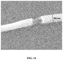
- FIG. 14 shows a single nanowire electrodeposited with one compositional modulation, released from template, dispersed on a substrate, and then etched to create a narrower region.
- the width of the nanowire as seen in FIG. 14 is approximately 306 nm.
- FIG. 15 shows a schematic of the fabrication of wires with notches using compositionally modulated wires.
- (a) Deposit wires of element 1 (or alloy with composition 1 ) on the insulating material.
- (b) Deposit element 2 (or alloy with composition 2 ) on the wires at the location the nanopores (nanogates).
- (c) The formation of compositional modulation in the wires occurs by inter-diffusion of the two elements (or alloys (compositions)).
- Element 2 (or alloy with composition 2 ) is removed.
- the selective etching of the modulated layer is performed to create the notches in the wire.
- (f) A 3-D sketch of the notches created by this process is shown.
- branched nanochannel devices Disclosed herein are branched nanochannel devices and methods for the detection and/or sorting of nucleic acids. Further disclosed are methods for the fabrication of branched nanochannel devices.
- nucleic acid as used herein means a polymer composed of nucleotides, e.g. deoxyribonucleotides or ribonucleotides.
- ribonucleic acid and “RNA” as used herein mean a polymer composed of ribonucleotides.
- deoxyribonucleic acid and “DNA” as used herein mean a polymer composed of deoxyribonucleotides.
- oligonucleotide denotes single- or double-stranded nucleotide multimers of from about 2 to up to about 100 nucleotides in length.
- Suitable oligonucleotides may be prepared by the phosphoramidite method described by Beaucage and Carruthers, Tetrahedron Lett., 22:1859-1862 (1981), or by the triester method according to Matteucci, et al., J. Am. Chem. Soc., 103:3185 (1981), both incorporated herein by reference, or by other chemical methods using either a commercial automated oligonucleotide synthesizer or VLSIPSTM technology.
- double-stranded When oligonucleotides are referred to as “double-stranded,” it is understood by those of skill in the art that a pair of oligonucleotides exist in a hydrogen-bonded, helical array typically associated with, for example, DNA.
- double-stranded As used herein is also meant to refer to those forms which include such structural features as bulges and loops, described more fully in such biochemistry texts as Stryer, Biochemistry , Third Ed., (1988), incorporated herein by reference for all purposes.
- polynucleotide refers to a single or double stranded polymer composed of nucleotide monomers. In some embodiments, the polynucleotide is composed of nucleotide monomers of generally greater than 100 nucleotides in length and up to about 8,000 or more nucleotides in length.
- polypeptide refers to a compound made up of a single chain of D- or L-amino acids or a mixture of D- and L-amino acids joined by peptide bonds.
- complementary refers to the topological compatibility or matching together of interacting surfaces of a probe molecule and its target.
- the target and its probe can be described as complementary, and furthermore, the contact surface characteristics are complementary to each other.
- hybridization or “hybridizes” refers to a process of establishing a non-covalent, sequence-specific interaction between two or more complementary strands of nucleic acids into a single hybrid, which in the case of two strands is referred to as a duplex.
- anneal refers to the process by which a single-stranded nucleic acid sequence pairs by hydrogen bonds to a complementary sequence, forming a double-stranded nucleic acid sequence, including the reformation (renaturation) of complementary strands that were separated by heat (thermally denatured).
- melting refers to the denaturation of a double-stranded nucleic acid sequence due to high temperatures, resulting in the separation of the double strand into two single strands by breaking the hydrogen bonds between the strands.
- Target refers to a molecule that has an affinity for a given probe. Targets may be naturally-occurring or man-made molecules. Also, they can be employed in their unaltered state or as aggregates with other species.
- a “subject” is meant an individual.
- the “subject” can include, for example, domesticated animals, such as cats, dogs, etc., livestock (e.g., cattle, horses, pigs, sheep, goats, etc.), laboratory animals (e.g., mouse, rabbit, rat, guinea pig, etc.) mammals, non-human mammals, primates, non-human primates, rodents, birds, reptiles, amphibians, fish, and any other animal.
- livestock e.g., cattle, horses, pigs, sheep, goats, etc.
- laboratory animals e.g., mouse, rabbit, rat, guinea pig, etc.
- mammals non-human mammals, primates, non-human primates, rodents, birds, reptiles, amphibians, fish, and any other animal.
- the subject can be a mammal such as a primate or a human.
- adjacent means, near, next to or adjoining.
- the adjacent nanopores are in close physical proximity, but are located in different nanochannels (for example, nanopores 2 and 3 in FIG. 3 ).
- the distance between the adjacent nanopores can be from 0.5 ⁇ m to 10 ⁇ m.
- a device comprising:
- the device further comprises an electrode within each of the three or more fluid chambers.
- the nanopore (or nanogate) can have a cross section shape that is round, square, or can be an irregular shape.
- the diameter of the cross section of the nanopore can be, for example, from 2 nm to 50 nm in diameter.
- the cross section of the nanopore can range from 2 nm ⁇ 2 nm to 50 nm ⁇ 50 nm.
- the area of the cross section of the nanopore can be from 4 to 2500 nm 2 .
- the nanopores are dimensioned to allow a linearized nucleic acid to pass through the nanopores.
- the nanopores have a diameter from 2 nm to 100 nm.
- the nanopores have a diameter from 10 nm to 20 nm.
- the nanopore is from 5 nm to 20 nm in diameter.
- the length of the nanopore can be from 10 nm to 300 nm. In a preferred embodiment, the length of the nanopore can be from 50 nm to 200 nm. In a more preferred embodiment, the length of the nanopore can be from 100 nm to 200 nm.
- the distance between the adjacent nanopores can be from 0.5 ⁇ m to 10 ⁇ m. In a preferred embodiment, the distance between the adjacent nanopores can be from 1 ⁇ m to 5 ⁇ m. In a more preferred embodiment, the distance between the adjacent nanopores can be from 1 ⁇ m to 3 ⁇ m.
- the nanochannel can have a cross section shape that is round, square, or can be an irregular shape.
- the diameter of the cross section of the nanochannel can be, for example, from 50 nm to 1000 nm in diameter.
- the cross section of the nanochannel can range from 50 nm ⁇ 50 nm to 1000 nm ⁇ 1000 nm.
- the area of the cross section of the nanopore can be from 2,500 to 1,000,000 nm 2 .
- the nanochannel has a diameter from 50 nm to 1000 nm.
- the nanochannel is from 100 nm-500 nm in diameter.
- the nanochannel has a diameter from 200 nm to 400 nm.
- the length of the nanochannel can be from 5 ⁇ m to 100 ⁇ m. In a preferred embodiment, the length of the nanochannel can be from 10 ⁇ m to 50 ⁇ m. In a more preferred embodiment, the length of the nanochannel can be from 10 ⁇ m to 30 ⁇ m.
- the nanopore and nanochannel are aligned. In one embodiment, the nanopore is located inside the nanochannel. In one embodiment, the nanochannel surrounds the nanopore.
- the fluid chamber can have a cross section shape that is round, square, or can be an irregular shape.
- the cross section of the fluid chamber can range from (2 ⁇ m to 1000 ⁇ m) ⁇ (1 ⁇ m to 10 ⁇ m).
- the area of the cross section of the nanopore can be from 4 to 10,000 ⁇ m 2 .
- the cross section of the fluid chamber is from (2 ⁇ m to 100 ⁇ m) ⁇ (1 ⁇ m to 5 ⁇ m).
- the cross section of the fluid chamber is from (5 ⁇ m to 10 ⁇ m) ⁇ (2 ⁇ m to 3 ⁇ m).
- the fluid chamber is 5 ⁇ m ⁇ 2 ⁇ m.
- the fluid chamber and nanochannel are aligned. In one embodiment, the nanochannel is connected to inside the fluid chamber.
- the insulating layer (or insulating material) is comprised of an oxide, nitride, phosphide, or ceramic.
- materials used for the insulating layer include, silicon oxide, silicon nitride, aluminum oxide, zirconia oxide, niobium oxide, boron nitride, indium phosphide, aluminum phosphide, and the like.
- the substrate has a flat surface.
- the substrate has is selected from, for example, wafers such as silicon, germanium, sapphire, gallium arsenide, indium phosphide, aluminum oxide, and the like.
- the substrate is composed of multiple layers of materials.
- the insulating layer is on top of the substrate.
- a method for detecting a nucleic acid comprising: introducing a nucleic acid into a fluid chamber of a device, wherein the device comprises:
- the nucleic acid is single stranded or double stranded. In one embodiment, the nucleic acid is single stranded and is hybridized with a single stranded nucleic acid probe to form a double stranded region at a target location of the nucleic acid. In one embodiment, the nucleic acid probe is from 15 to 1000 nucleotides. In one embodiment, the current blockage comprises different steps for the single stranded nucleic acid and the double stranded region.
- the nucleic acid comprises an attachment at a target location of the nucleic acid.
- the attachment is selected from protein, metal particles, inorganic particles, a nucleic acid fragment, a nucleic acid fragment with a protein, or a nucleic acid fragment with a particle.
- the current blockage comprises different steps for the nucleic acid and the attachment.
- the nanopores have a diameter from 2 nm to 100 nm. In one embodiment, the nanopores have a diameter from 10 nm to 20 nm.
- the adjacent nanopores are from 0.5 ⁇ m to 10 ⁇ m apart. In one embodiment, the adjacent nanopores are from 1 ⁇ m to 3 ⁇ m apart.
- the nanochannel has a diameter from 50 nm to 1000 nm. In one embodiment, the nanochannel has a diameter from 200 nm to 400 nm. In one embodiment, the nanochannel has a length from 5 ⁇ m to 100 ⁇ m. In one embodiment, the nanochannel has a length from 10 ⁇ m to 30 ⁇ m.
- a method for sorting a nucleic acid comprising: introducing a nucleic acid into a fluid chamber of a device, wherein the device comprises:
- the electric potential is adjusted based on the measurement of an electrical current.
- the two or more different electric potentials applied on the two or more adjacent nanopores on different branches of the branched nanochannel is adjusted based on the measurement of electrical currents across the adjacent nanopores.
- the adjustment of the electrical potentials allows the nucleic acid to be sorted into different fluid chambers connected to different branches of the branched nanochannel.
- a method for fabricating a branched nanochannel device comprising:
- the insulating layer is comprised of silicon oxide, silicon nitride, aluminum oxide, zirconia oxide, niobium oxide, boron nitride, indium phosphide, aluminum phosphide, or combinations thereof.
- the additional insulating layer is comprised of silicon oxide, silicon nitride, aluminum oxide, zirconia oxide, niobium oxide, boron nitride, indium phosphide, aluminum phosphide, or combinations thereof.
- the substrate is comprised of silicon, germanium, sapphire, gallium arsenide, indium phosphide, aluminum oxide, or combinations thereof.
- a method for fabricating a branched nanochannel device comprising:
- the metal wire comprises a metal or alloy of elements selected from Cr, Mn, Ni, Fe, Co, Cu, Zn, Ga, Ge, Mo, Ru, Rh, Pd, Ag, Cd, In, Sn, Sb, Te, Re, Pt, Au, Pb, or Bi.
- the metal wire comprises an alloy selected from NiFe, NiFeCo, NiFeCu, CoFeCu, NiZn, NiFeZn, CuZn, NiFePd, CuPd, or CuIn.
- the metal wire comprises a NiFe alloy with Ni content between 20 to 100 wt % and Fe content between 0 to 80 wt %.
- the template is comprised of aluminum oxide, silicon oxide, or polycarbonate.
- the notches are created by etching one of the metals or alloys in the metal wire in a solution comprising nitric acid, sulfuric acid, phosphoric acid, chromium oxide, ferric chloride, potassium permanganate, citric acid, tartaric acid, or oxalic acid.
- a method for fabricating a branched nanochannel device comprising:
- the first material is selected from Cr, Mn, Ni, Fe, Co, Cu, Zn, Ga, Ge, Mo, Ru, Rh, Pd, Ag, Cd, In, Sn, Sb, Te, Re, Pt, Au, Pb, or Bi.
- the second material is selected from Cr, Mn, Ni, Fe, Co, Cu, Zn, Ga, Ge, Mo, Ru, Rh, Pd, Ag, Cd, In, Sn, Sb, Te, Re, Pt, Au, Pb, or Bi.
- the first material is selected from Ni, Cu, or Ag the second material is selected from Co, Fe, Zn, Ga, In, or Sn.
- the metal wires of the first and second materials can be deposited with methods selected from sputtering, physical vapor deposition, evaporation, chemical vapor deposition, atomic layer deposition, electrodeposition and the combination of such.
- the metal wires are formed using methods selected from optical lithography, UV lithography, electron beam lithography, assembly, lift off, sputter etching, chemical etching, plasma etching.
- the inter-diffusing is conducted at 100° C. to 800° C.
- the second metal wire of the second material is removed by etching in a solution comprising nitric acid, sulfuric acid, phosphoric acid, chromium oxide, ferric chloride, potassium permanganate, citric acid, tartaric acid, or oxalic acid.
- the notches are created by etching the locations of overlap on the branched first metal wire of the first material in a solution comprising nitric acid, sulfuric acid, phosphoric acid, chromium oxide, ferric chloride, potassium permanganate, citric acid, tartaric acid, or oxalic acid.
- the notches have a diameter from 2 nm to 100 nm. In one embodiment, the notches have a diameter from 10 nm to 20 nm.
- the adjacent notches are from 0.5 ⁇ m to 10 ⁇ m apart. In one embodiment, the adjacent notches are from 1 ⁇ m to 3 ⁇ m apart.
- the nanochannel has a diameter from 50 nm to 1000 nm. In one embodiment, the nanochannel has a diameter from 200 nm to 400 nm. In one embodiment, the nanochannel has a length from 5 ⁇ m to 100 ⁇ m. In one embodiment, the nanochannel has a length from 10 ⁇ m to 30 ⁇ m.
- This example discloses various types of branched nanochannel devices.
- the conductance between the two electrolytes are determined by the conductance across the pore, which is related to the area (size) of the pore.
- This conductance can be measured as the electric current between a pair of electrodes placed in the two electrolytes ( FIG. 1 ).
- the electrolyte can be for example, potassium chloride.
- detection of DNA molecules through a nanopore (or nanogate) is shown according to FIG. 2 .
- the current measured across a nanopore between two electrodes FIG. 2 a ).
- the current across a nanopore is blocked by a strand of DNA when it is passing through the nanopore.
- the DNA is passing across the pore because of the electrophoretic force on the negatively charged DNA molecule.
- the current blockage is observed when the pore is small, for example, under 20 nm in diameter ( FIG. 2 b ).
- the configuration of DNA when it passes across the pore can be differentiated.
- a deeper current blockage is typically observed when a folded DNA pass through because of the larger ( FIG. 2 c ).
- FIG. 3 An example of a branched nanochannel device according to the invention is shown in FIG. 3 .
- the insulating layer 101 is supported on top of a substrate 102 .
- the substrate 102 can be for example, silicon, germanium, sapphire, oxides, and the like.
- the device has nanochannels 8 which connect the fluid chambers 9 (fluid chambers can also be referred to as microfluidic channels as well).
- the device has nanopores 1 , 2 , and 3 in the nanochannels 8 .
- the device has two nanopores 2 and 3 that are adjacent to each other.
- the fluid chambers 9 can be of any shape that allows fluid to pass through to the nanochannels 8 .
- the nanochannels 8 can have different shapes (for example, can be curved) and do not have to be straight.
- FIG. 4 shows the top down view of the device.
- the device has nanochannels 8 which connect the fluid chambers 9 .
- the device has nanopores 2 , 3 , 4 , and 5 in the nanochannels 8 .
- the device has at least two nanopores 2 and 3 that are adjacent to each other.
- the device can comprise an additional pair of adjacent nanopores 4 and 5 .
- the fluid chambers 9 can be of any shape that allows fluid to pass through to the nanochannels 8 .
- the nanochannels 8 can have different shapes (for example, can be curved) and do not have to be straight.
- FIG. 5 shows the top down view of the device.
- the device has nanochannels 8 which connect the fluid chambers 9 .
- the device has nanopores 1 , 2 , 3 , 4 , 5 , and 6 in the nanochannels 8 .
- the device has at least two nanopores 2 and 3 that are adjacent to each other.
- the device can comprise an additional number of nanopores 4 , 5 , and 6 , where the additional nanopores are optionally adjacent to one another.
- the fluid chambers 9 can be of any shape that allows fluid to pass through to the nanochannels 8 .
- the nanochannels 8 can have different shapes (for example, can be curved) and do not have to be straight.
- FIG. 6 shows the top down view of the device.
- the device has nanochannels 8 which connect the fluid chambers 9 .
- the device has nanopores 1 , 2 , and 3 in the nanochannels 8 .
- the device has at least two nanopores 2 and 3 that are adjacent to each other.
- the fluid chambers 9 can be of any shape that allows fluid to pass through to the nanochannels 8 .
- the nanochannels 8 can have different shapes (for example, can be curved, as shown in FIG. 6 ) and do not have to be straight.
- the nanochannels and nanopore are present in an insulating layer 101 .
- FIG. 7 shows the top down view of the device.
- the device has nanochannels 8 which connect the fluid chambers 9 .
- the device has nanopores 1 , 2 , 3 , 4 , and 5 in the nanochannels 8 .
- the device has at least two nanopores 2 and 3 that are adjacent to each other.
- the device can comprise an additional pair of adjacent nanopores 4 and 5 .
- the fluid chambers 9 can be of any shape that allows fluid to pass through to the nanochannels 8 .
- the nanochannels 8 can have different shapes (for example, can be curved) and do not have to be straight.
- This example discloses various methods for detection and/or sorting of nucleic acids using the branched nanochannel devices disclosed herein.
- FIG. 8 shows the top down view of the device.
- the device has nanochannels which connect the fluid chambers.
- the device has nanopores 1 , 2 , and 3 in the nanochannels.
- the device has at least two nanopores 2 and 3 that are adjacent to each other.
- the fluid chambers can be of any shape that allows fluid to pass through to the nanochannels.
- the nanochannels can have different shapes (for example, can be curved, as shown in FIG. 8 ) and do not have to be straight.
- the nanochannels and nanopore are present in an insulating layer 101 .
- An electrode is present in each of the fluid chambers.
- the four electrodes (E 1 , E 2 , E 3 , and E 4 ) are controlled separately, and can have four different voltages.
- E 1 is at the lowest potential.
- E 2 is more positive than E 1
- E 3 and E 4 are more positive than E 2 .
- E 2 ⁇ E 1 0-2 V, preferably, 50-800 mV. This is the voltage applied on nanogate #1.
- E 3 ⁇ E 2 0-2 V, preferably, 50-800 mV. This is the voltage applied on nanogate #3.
- E 4 ⁇ E 2 0-2 V, preferably, 50-800 mV. This is the voltage applied on nanogate #2.
- the nucleic acid (DNA) to be analyzed is introduced in the fluid chamber with electrode E 1 .
- the negatively charged DNA is then pulled through the nanopore 1 .
- DNA strands that are recognized by a nucleic acid probe to a target gene can be differentiated from the DNA strands without the target gene because this creates a deeper current blockage as the DNA passes through a nanopore.
- the nucleic acid probe can be a single stranded nucleic acid only, or can have attachment selected from protein, particles, polymers, and the combination of such.
- the voltages on nanopores 2 and 3 are controlled by E 3 -E 2 and E 4 -E 2 during the detection of genes on DNA and they can be used to pull the DNA to one of the two nanopores, 2 or 3 , based on the detection of the genes.
- Another embodiment uses the device in FIG. 7 to sort the nucleic acid.
- the voltages on nanopores 4 and 5 are controlled based on the detection of genes on nanopore 2 .
- the nucleic acid is thus pulled into one of the two nanopores 4 or 5 based on the detection of genes.
- Yet another embodiment uses the device in FIG. 5 to sort the nucleic acid.
- the voltages on nanopores 4 , 5 , 6 are controlled based on the detection of genes on nanopore 2 .
- the nucleic acid is thus pulled into one of the three nanopores 4 or 5 or 6 based on the detection of genes.
- the frequency of this passage increases as the ⁇ E 1 E 2 increases.
- the speed of passage also depends on ⁇ E 1 E 2 .
- the speed of passage is controlled by the competition between ⁇ E 2 E 4 and ⁇ E 2 E 3 .
- the voltage ⁇ E 2 E 3 on nanopore 3 also attracts DNA and slows down the passage of the DNA on nanopore 2 .
- DNA can also pass on nanopore 3 if the electrophoretic force by nanopore ⁇ E 2 E 3 is stronger.
- the current blockage depends on the cross section of the DNA.
- the genes on the DNA can be detected after labelling.
- the relative location of the genes on the DNA can be detected. For example, as seen in FIG. 10 c , the deeper current blockage in the middle of the whole blockage because the gene is in the middle of the DNA.
- Nanopores 2 and 3 can be used to detect the presence of the gene on the DNA.
- the voltage on nanopores 4 , 5 , and 6 can be controlled according to the detection results.
- the DNA can then be sorted into different branches of the branched nanochannel and fluid chambers based on the gene detection results. In this method, the DNA can be sorted by the presence (or absence) of the target gene of interest.
- This example discloses various methods for fabrication of the branched nanochannel devices disclosed herein.
- FIG. 12 shows the subtractive etching of shape modulated wires to make channels with pores.
- the branched nanochannel device can be made by fabricating wires with notches, followed by embedding the wires in the insulating material, and subtractively etching (removing) these wires. The channels are then created in the insulating materials by removing the wires. The nanogates (or nanopores) are created at the locations where the notches are located along the wires.
- the branched nanochannel device can be fabricated by use of compositionally modulated wires.
- the wires can be fabricated with electrodeposition.
- the wires comprise layers with different compositions (metals of alloys).
- the layers comprising the different compositions can be electrodeposited with pulsed potential, pulsed current, or pulsed agitation.
- NiFe alloys wires are electrodeposited along with alloys of different compositions at different potentials.
- the layers with different compositions are etched differently with various etching chemistries. Layers with certain compositions are etched and preferably creating notches along the wires.
- FIG. 14 a single nanowire electrodeposited with one compositional modulation, released from template, dispersed on a substrate, and then etched to create a narrower region is shown. The nanowire is then capped and etched to create the channel.
- Example templates include aluminum oxide templates, diblock copolymer templates, or nuclear track etched templates.
- the template can also be fabricated in other ways to create branches.
- the template is dissolved to release the wires.
- direct electrodeposition can be used to form free wires with modulated compositions, such as electrochemical 3-dimensional printing.
- the free wires can be etched such that one layer of the compositions are selectively etched to create notched regions along the wires.
- the wires with notches are collected in liquid solution and dispersed on insulating layer on the substrate.
- the fabrication methods are further shown in FIG. 15 .
- Fourth, element 2 (or alloy with composition 2 ) is removed.
- the selective etching of the modulated layer is performed to create the notches in the wire. As further shown in FIG. 15 , a 3-D sketch of the notches created by this process is shown.
- the formation of the compositional modulation in the wires can also be achieved by other methods, for example, inter-diffusion of material at high temperature, implantation, or direct deposition (bombarding) of the second material.
- the formation of wires can be achieved with processes such as deposition (PVD, sputtering, evaporation, electrodeposition, CVD), followed by lithography patterning, followed by etching (dry etching or wet etching), and followed by pattern removal.
- wires can be formed by lithography patterning followed by deposition (evaporation, electrodeposition), and followed by lift-off.
- the fluid chambers can be formed by processes such as deposition of insulating materials, lithography patterning, etching of insulting materials, and bonding.
Landscapes
- Chemical & Material Sciences (AREA)
- Health & Medical Sciences (AREA)
- Life Sciences & Earth Sciences (AREA)
- Engineering & Computer Science (AREA)
- Physics & Mathematics (AREA)
- Analytical Chemistry (AREA)
- Organic Chemistry (AREA)
- Molecular Biology (AREA)
- General Health & Medical Sciences (AREA)
- Chemical Kinetics & Catalysis (AREA)
- Biochemistry (AREA)
- Immunology (AREA)
- Electrochemistry (AREA)
- Biomedical Technology (AREA)
- Wood Science & Technology (AREA)
- Zoology (AREA)
- Hematology (AREA)
- General Physics & Mathematics (AREA)
- Pathology (AREA)
- Proteomics, Peptides & Aminoacids (AREA)
- Dispersion Chemistry (AREA)
- Materials Engineering (AREA)
- Metallurgy (AREA)
- Biophysics (AREA)
- Nanotechnology (AREA)
- Clinical Laboratory Science (AREA)
- Genetics & Genomics (AREA)
- Microbiology (AREA)
- General Engineering & Computer Science (AREA)
- Bioinformatics & Cheminformatics (AREA)
- Biotechnology (AREA)
- Fluid Mechanics (AREA)
- Spectroscopy & Molecular Physics (AREA)
- Urology & Nephrology (AREA)
- Medicinal Chemistry (AREA)
- Food Science & Technology (AREA)
- Crystallography & Structural Chemistry (AREA)
- Measuring Or Testing Involving Enzymes Or Micro-Organisms (AREA)
- Apparatus Associated With Microorganisms And Enzymes (AREA)
- Investigating Or Analyzing Materials By The Use Of Electric Means (AREA)
Abstract
Description
-
- a branched nanochannel;
- three or more fluid chambers connected by the branched nanochannel;
- an electrode within each of the three or more fluid chambers; and
- three or more nanopores in the branched nanochannel;
- wherein two or more nanopores are adjacent to each other on different branches of the branched nanochannel;
- applying an electric potential across each pair of electrodes in the fluid chambers;
- wherein two or more different electric potentials are applied on the two or more nanopores adjacent to each other on different branches of the branched nanochannel;
- measuring an electric current across each pair of electrodes in the fluid chambers; and
- detecting the passage of nucleic acid through the nanopores as current blockage of the nanopores.
- depositing an insulating layer on top of a substrate;
- creating a branched wire on the insulating layer, wherein the branched wire comprises three or more branches and three or more notches on the branched wire, wherein two or more notches are adjacent to each other on different branches of the branched wire;
- depositing an additional insulating layer on top of the branched wire; and
- removing the branched wire to form a branched nanochannel.
- electrodepositing a metal wire into a template, wherein the metal wire comprises two or more metals or alloys;
- dissolving the template;
- creating notches by etching one of the metals or alloys in the metal wire;
- collecting the metal wire; and
- dispersing the metal wire onto the insulating layer.
- depositing a branched first metal wire of a first material on the insulating layer;
- depositing one or more metal wires of a second material on the insulating layer, wherein the second material is different from the first material and the one or more metal wires of the second material overlap with the branched first metal wire of the first material at locations where the notches are to be placed;
- inter-diffusing the second material into the first material at the locations of the overlaps by heating the substrate and wires to form a hybrid wire portion;
- removing the one or more metal wires of the second material except for the locations of overlaps; and
- creating notches on the branched first metal wire of the first material by etching the hybrid wire portion at the locations of overlaps.
-
- a branched nanochannel;
- three or more fluid chambers connected by the branched nanochannel;
- an electrode within each of the three or more fluid chambers; and
- three or more nanopores in the branched nanochannel;
- wherein two or more nanopores are adjacent to each other on different branches of the branched nanochannel;
- applying an electric potential across each pair of electrodes in the fluid chambers;
- wherein two or more different electric potentials are applied on the two or more nanopores adjacent to each other on different branches of the branched nanochannel;
- measuring an electric current across each pair of electrodes in the fluid chambers; and
- detecting the passage of nucleic acid through the nanopores as current blockage of the nanopores.
-
- a branched nanochannel;
- three or more fluid chambers connected by the branched nanochannel;
- an electrode within each of the three or more fluid chambers; and
- three or more nanopores in the branched nanochannel;
- wherein two or more nanopores are adjacent to each other on different branches of the branched nanochannel;
- applying an electric potential across each pair of electrodes in the fluid chambers;
- wherein two or more different electric potentials are applied on the two or more nanopores adjacent to each other on different branches of the branched nanochannel;
- measuring an electric current across each pair of electrodes in the fluid chambers; and
- sorting the nucleic acid into a fluid chamber.
- depositing an insulating layer on top of a substrate;
- creating a branched wire on the insulating layer, wherein the branched wire comprises three or more branches and three or more notches on the branched wire, wherein two or more notches are adjacent to each other on different branches of the branched wire;
- depositing an additional insulating layer on top of the branched wire; and
- removing the branched wire to form a branched nanochannel.
- depositing an insulating layer on top of a substrate;
- creating a branched wire on the insulating layer;
- wherein the branched wire comprises three or more branches and three or more notches on the branched wire, wherein two or more notches are adjacent to each other on different branches of the branched wire;
- wherein the branched wire is created by a method comprising:
- electrodepositing a metal wire into a template, wherein the metal wire comprises two or more metals or alloys;
- dissolving the template;
- creating notches by etching one of the metals or alloys in the metal wire;
- collecting the metal wire; and
- dispersing the metal wire onto the insulating layer;
- depositing an additional insulating layer on top of the branched wire; and
- removing the branched wire to form a branched nanochannel.
- depositing an insulating layer on top of a substrate;
- creating a branched wire on the insulating layer;
- wherein the branched wire comprises three or more branches and three or more notches on the branched wire, wherein two or more notches are adjacent to each other on different branches of the branched wire;
- wherein the branched wire is created by a method comprising:
- depositing a branched first metal wire of a first material on the insulating layer;
- depositing one or more metal wires of a second material on the insulating layer, wherein the second material is different from the first material and the one or more metal wires of the second material overlap with the branched first metal wire of the first material at locations where the notches are to be placed;
- inter-diffusing the second material into the first material at the locations of the overlaps by heating the substrate and wires to form a hybrid wire portion;
- removing the one or more metal wires of the second material except for the locations of overlaps; and
- creating notches on the branched first metal wire of the first material by etching the hybrid wire portion at the locations of overlaps;
- depositing an additional insulating layer on top of the branched wire; and
- removing the branched wire to form a branched nanochannel.
Claims (6)
Priority Applications (2)
| Application Number | Priority Date | Filing Date | Title |
|---|---|---|---|
| US15/875,248 US10974244B2 (en) | 2017-01-19 | 2018-01-19 | Branched nanochannel devices for detection and sorting of nucleic acids |
| US17/199,656 US12023673B2 (en) | 2017-01-19 | 2021-03-12 | Branched nanochannel devices for detection and sorting of nucleic acids |
Applications Claiming Priority (2)
| Application Number | Priority Date | Filing Date | Title |
|---|---|---|---|
| US201762448115P | 2017-01-19 | 2017-01-19 | |
| US15/875,248 US10974244B2 (en) | 2017-01-19 | 2018-01-19 | Branched nanochannel devices for detection and sorting of nucleic acids |
Related Child Applications (1)
| Application Number | Title | Priority Date | Filing Date |
|---|---|---|---|
| US17/199,656 Division US12023673B2 (en) | 2017-01-19 | 2021-03-12 | Branched nanochannel devices for detection and sorting of nucleic acids |
Publications (2)
| Publication Number | Publication Date |
|---|---|
| US20180200716A1 US20180200716A1 (en) | 2018-07-19 |
| US10974244B2 true US10974244B2 (en) | 2021-04-13 |
Family
ID=62838819
Family Applications (2)
| Application Number | Title | Priority Date | Filing Date |
|---|---|---|---|
| US15/875,248 Active 2038-09-03 US10974244B2 (en) | 2017-01-19 | 2018-01-19 | Branched nanochannel devices for detection and sorting of nucleic acids |
| US17/199,656 Active 2039-11-27 US12023673B2 (en) | 2017-01-19 | 2021-03-12 | Branched nanochannel devices for detection and sorting of nucleic acids |
Family Applications After (1)
| Application Number | Title | Priority Date | Filing Date |
|---|---|---|---|
| US17/199,656 Active 2039-11-27 US12023673B2 (en) | 2017-01-19 | 2021-03-12 | Branched nanochannel devices for detection and sorting of nucleic acids |
Country Status (1)
| Country | Link |
|---|---|
| US (2) | US10974244B2 (en) |
Families Citing this family (1)
| Publication number | Priority date | Publication date | Assignee | Title |
|---|---|---|---|---|
| EP3850362A4 (en) * | 2018-09-14 | 2022-06-08 | Applied Materials, Inc. | METHOD OF FORMING A NANOPOORE AND RESULTING STRUCTURE |
Citations (4)
| Publication number | Priority date | Publication date | Assignee | Title |
|---|---|---|---|---|
| US20060073489A1 (en) * | 2004-10-05 | 2006-04-06 | Gangqiang Li | Nanopore separation devices and methods of using same |
| US20090305273A1 (en) * | 2006-07-19 | 2009-12-10 | Bionanomatrix, Inc. | Nanonozzle device arrays: their preparation and use for macromolecular analysis |
| US20110053284A1 (en) * | 2007-05-08 | 2011-03-03 | The Trustees Of Boston University | Chemical functionalization of solid-state nanopores and nanopore arrays and applications thereof |
| US20130256118A1 (en) * | 2010-05-11 | 2013-10-03 | Trustees Of Boston University | Use of Nanopore Arrays For Multiplex Sequencing of Nucleic Acids |
Family Cites Families (2)
| Publication number | Priority date | Publication date | Assignee | Title |
|---|---|---|---|---|
| EP2313758B1 (en) * | 2008-07-17 | 2012-02-01 | Koninklijke Philips Electronics N.V. | Nanopore device and a method for nucleic acid analysis |
| US9017937B1 (en) * | 2009-04-10 | 2015-04-28 | Pacific Biosciences Of California, Inc. | Nanopore sequencing using ratiometric impedance |
-
2018
- 2018-01-19 US US15/875,248 patent/US10974244B2/en active Active
-
2021
- 2021-03-12 US US17/199,656 patent/US12023673B2/en active Active
Patent Citations (4)
| Publication number | Priority date | Publication date | Assignee | Title |
|---|---|---|---|---|
| US20060073489A1 (en) * | 2004-10-05 | 2006-04-06 | Gangqiang Li | Nanopore separation devices and methods of using same |
| US20090305273A1 (en) * | 2006-07-19 | 2009-12-10 | Bionanomatrix, Inc. | Nanonozzle device arrays: their preparation and use for macromolecular analysis |
| US20110053284A1 (en) * | 2007-05-08 | 2011-03-03 | The Trustees Of Boston University | Chemical functionalization of solid-state nanopores and nanopore arrays and applications thereof |
| US20130256118A1 (en) * | 2010-05-11 | 2013-10-03 | Trustees Of Boston University | Use of Nanopore Arrays For Multiplex Sequencing of Nucleic Acids |
Non-Patent Citations (3)
| Title |
|---|
| Beaucage and Carruthers, "Deoxynucleoside phosphoramidites-A new class of key intermediates for deoxypolynucleotide synthesis", Tetrahedron Lett., 22:1859-1862 (1981). |
| Beaucage and Carruthers, "Deoxynucleoside phosphoramidites—A new class of key intermediates for deoxypolynucleotide synthesis", Tetrahedron Lett., 22:1859-1862 (1981). |
| Matteucci, et al., "Synthesis of deoxyoligonucleotides on a polymer support", J. Am. Chem. Soc., 103:3185-3191 (1981). |
Also Published As
| Publication number | Publication date |
|---|---|
| US20210197198A1 (en) | 2021-07-01 |
| US20180200716A1 (en) | 2018-07-19 |
| US12023673B2 (en) | 2024-07-02 |
Similar Documents
| Publication | Publication Date | Title |
|---|---|---|
| KR101963462B1 (en) | Systems and methods for automated reusable parallel biological reactions | |
| EP2156179B1 (en) | Methods for using a nanopore | |
| US9816129B2 (en) | Bioprobes and methods of use thereof | |
| EP3075867B1 (en) | Sensing strategies and methods for nucleic acid detection using biosensors | |
| US20060057604A1 (en) | Method for electrically detecting oligo-nucleotides with nano-particles | |
| US20250145982A1 (en) | System and method for preparing a sequencing device | |
| US20250222451A1 (en) | Electronic assembly of long dna molecules | |
| DE10240094B4 (en) | Component for the detection of biological material and method and device for the detection of biological material | |
| Wang et al. | Detection of single tumor cell resistance with aptamer biochip | |
| US12023673B2 (en) | Branched nanochannel devices for detection and sorting of nucleic acids | |
| Báez et al. | Effects of preparation on catalytic, magnetic and hybrid micromotors on their functional features and application in gastric cancer biomarker detection | |
| EP2883961B1 (en) | A nucleic acid analysis method and apparatus | |
| Zhao et al. | Translocation of tetrahedral DNA nanostructures through a solid-state nanopore | |
| US10738349B2 (en) | Polynucleotide based movement, kits and methods related thereto | |
| Borghei et al. | Building Polyvalent DNA‐Functionalized Anisotropic AuNPs Using Poly‐Guanine‐Mediated In‐Situ Synthesis for LSPR‐Based Assays: Case Study on OncomiR‐155 | |
| US20160265064A1 (en) | Electrochemical clamp assay | |
| Xi et al. | The detection of HBV DNA with gold-coated iron oxide nanoparticle gene probes | |
| Loh et al. | An All-Electric Single-Molecule Hybridisation Detector for short DNA Fragments | |
| Tien et al. | Improving gold nanowire-based biosensor sensitivity by changing probe design | |
| Vasilyeva | Detection of the BCR-ABL leukemia gene fusion using chip-based electrochemical assay | |
| Wang et al. | Methods and Techniques in Molecular Toxicology of Nanomaterials | |
| JP2002335962A (en) | Device and method for concentrating gene | |
| Moretti | Synthetic nanopores and nanoparticles for the detection and the manipulation of biological molecules. | |
| HK1141587B (en) | Methods for using a nanopore | |
| DE19548590A1 (en) | Solid carrier with different nucleic acid analogues at different surface positions |
Legal Events
| Date | Code | Title | Description |
|---|---|---|---|
| FEPP | Fee payment procedure |
Free format text: ENTITY STATUS SET TO UNDISCOUNTED (ORIGINAL EVENT CODE: BIG.); ENTITY STATUS OF PATENT OWNER: SMALL ENTITY |
|
| FEPP | Fee payment procedure |
Free format text: ENTITY STATUS SET TO SMALL (ORIGINAL EVENT CODE: SMAL); ENTITY STATUS OF PATENT OWNER: SMALL ENTITY |
|
| STPP | Information on status: patent application and granting procedure in general |
Free format text: DOCKETED NEW CASE - READY FOR EXAMINATION |
|
| AS | Assignment |
Owner name: THE BOARD OF TRUSTEES OF THE UNIVERSITY OF ALABAMA, ALABAMA Free format text: ASSIGNMENT OF ASSIGNORS INTEREST;ASSIGNOR:HUANG, QIANG;REEL/FRAME:046510/0693 Effective date: 20180719 Owner name: THE BOARD OF TRUSTEES OF THE UNIVERSITY OF ALABAMA Free format text: ASSIGNMENT OF ASSIGNORS INTEREST;ASSIGNOR:HUANG, QIANG;REEL/FRAME:046510/0693 Effective date: 20180719 |
|
| STPP | Information on status: patent application and granting procedure in general |
Free format text: NON FINAL ACTION MAILED |
|
| STPP | Information on status: patent application and granting procedure in general |
Free format text: RESPONSE TO NON-FINAL OFFICE ACTION ENTERED AND FORWARDED TO EXAMINER |
|
| STPP | Information on status: patent application and granting procedure in general |
Free format text: ADVISORY ACTION MAILED |
|
| STPP | Information on status: patent application and granting procedure in general |
Free format text: NON FINAL ACTION MAILED |
|
| STPP | Information on status: patent application and granting procedure in general |
Free format text: NOTICE OF ALLOWANCE MAILED -- APPLICATION RECEIVED IN OFFICE OF PUBLICATIONS |
|
| STPP | Information on status: patent application and granting procedure in general |
Free format text: PUBLICATIONS -- ISSUE FEE PAYMENT RECEIVED |
|
| STPP | Information on status: patent application and granting procedure in general |
Free format text: PUBLICATIONS -- ISSUE FEE PAYMENT VERIFIED |
|
| STCF | Information on status: patent grant |
Free format text: PATENTED CASE |
|
| MAFP | Maintenance fee payment |
Free format text: PAYMENT OF MAINTENANCE FEE, 4TH YR, SMALL ENTITY (ORIGINAL EVENT CODE: M2551); ENTITY STATUS OF PATENT OWNER: SMALL ENTITY Year of fee payment: 4 |