US10972121B2 - System and method for signal resampling - Google Patents
System and method for signal resampling Download PDFInfo
- Publication number
- US10972121B2 US10972121B2 US16/720,852 US201916720852A US10972121B2 US 10972121 B2 US10972121 B2 US 10972121B2 US 201916720852 A US201916720852 A US 201916720852A US 10972121 B2 US10972121 B2 US 10972121B2
- Authority
- US
- United States
- Prior art keywords
- signal data
- filter
- instrument
- signal
- input
- Prior art date
- Legal status (The legal status is an assumption and is not a legal conclusion. Google has not performed a legal analysis and makes no representation as to the accuracy of the status listed.)
- Active
Links
Images


Classifications
-
- H—ELECTRICITY
- H03—ELECTRONIC CIRCUITRY
- H03M—CODING; DECODING; CODE CONVERSION IN GENERAL
- H03M3/00—Conversion of analogue values to or from differential modulation
- H03M3/30—Delta-sigma modulation
- H03M3/39—Structural details of delta-sigma modulators, e.g. incremental delta-sigma modulators
- H03M3/412—Structural details of delta-sigma modulators, e.g. incremental delta-sigma modulators characterised by the number of quantisers and their type and resolution
- H03M3/414—Structural details of delta-sigma modulators, e.g. incremental delta-sigma modulators characterised by the number of quantisers and their type and resolution having multiple quantisers arranged in cascaded loops, each of the second and further loops processing the quantisation error of the loop preceding it, i.e. multiple stage noise shaping [MASH] type
-
- H—ELECTRICITY
- H03—ELECTRONIC CIRCUITRY
- H03H—IMPEDANCE NETWORKS, e.g. RESONANT CIRCUITS; RESONATORS
- H03H17/00—Networks using digital techniques
- H03H17/02—Frequency selective networks
- H03H17/06—Non-recursive filters
- H03H17/0621—Non-recursive filters with input-sampling frequency and output-delivery frequency which differ, e.g. extrapolation; Anti-aliasing
- H03H17/0635—Non-recursive filters with input-sampling frequency and output-delivery frequency which differ, e.g. extrapolation; Anti-aliasing characterized by the ratio between the input-sampling and output-delivery frequencies
- H03H17/0642—Non-recursive filters with input-sampling frequency and output-delivery frequency which differ, e.g. extrapolation; Anti-aliasing characterized by the ratio between the input-sampling and output-delivery frequencies the ratio being arbitrary or irrational
-
- G—PHYSICS
- G06—COMPUTING OR CALCULATING; COUNTING
- G06F—ELECTRIC DIGITAL DATA PROCESSING
- G06F1/00—Details not covered by groups G06F3/00 - G06F13/00 and G06F21/00
- G06F1/02—Digital function generators
- G06F1/022—Waveform generators, i.e. devices for generating periodical functions of time, e.g. direct digital synthesizers
-
- H—ELECTRICITY
- H03—ELECTRONIC CIRCUITRY
- H03M—CODING; DECODING; CODE CONVERSION IN GENERAL
- H03M3/00—Conversion of analogue values to or from differential modulation
- H03M3/30—Delta-sigma modulation
- H03M3/322—Continuously compensating for, or preventing, undesired influence of physical parameters
-
- H—ELECTRICITY
- H03—ELECTRONIC CIRCUITRY
- H03M—CODING; DECODING; CODE CONVERSION IN GENERAL
- H03M7/00—Conversion of a code where information is represented by a given sequence or number of digits to a code where the same, similar or subset of information is represented by a different sequence or number of digits
- H03M7/30—Compression; Expansion; Suppression of unnecessary data, e.g. redundancy reduction
- H03M7/3002—Conversion to or from differential modulation
- H03M7/3004—Digital delta-sigma modulation
- H03M7/3015—Structural details of digital delta-sigma modulators
- H03M7/302—Structural details of digital delta-sigma modulators characterised by the number of quantisers and their type and resolution
- H03M7/3022—Structural details of digital delta-sigma modulators characterised by the number of quantisers and their type and resolution having multiple quantisers arranged in cascaded loops, each of the second and further loops processing the quantisation error of the loop preceding it, i.e. multiple stage noise shaping [MASH] type
-
- H—ELECTRICITY
- H03—ELECTRONIC CIRCUITRY
- H03M—CODING; DECODING; CODE CONVERSION IN GENERAL
- H03M1/00—Analogue/digital conversion; Digital/analogue conversion
- H03M1/06—Continuously compensating for, or preventing, undesired influence of physical parameters
-
- H—ELECTRICITY
- H03—ELECTRONIC CIRCUITRY
- H03M—CODING; DECODING; CODE CONVERSION IN GENERAL
- H03M1/00—Analogue/digital conversion; Digital/analogue conversion
- H03M1/10—Calibration or testing
- H03M1/1009—Calibration
-
- H—ELECTRICITY
- H03—ELECTRONIC CIRCUITRY
- H03M—CODING; DECODING; CODE CONVERSION IN GENERAL
- H03M1/00—Analogue/digital conversion; Digital/analogue conversion
- H03M1/12—Analogue/digital converters
Definitions
- the present disclosure relates generally to instrument systems and methods of signal processing, and, more specifically, instrument systems and methods of resampling signal data from a first sample rate to a second sample rate different than the first sample rate.
- Signal processing and analysis is an essential aspect in today's highly technological world. Often times, signals are generated or recorded by one device and then processed and or analyzed by a separate test instrument. It may be desirable for the test instrument to be capable of signal processing and analysis in two different ways: 1) off-line with recorded signal data; and 2) real-time with an appropriate connection to the source of the signal data.
- RF radio frequency
- the sampling period T of the first device may be different than the sampling period T′ of the second device.
- the conversion from the waveform's sample rate to the test instrument's sample rate is not easy to perform because the test instrument may have a predefined sample rate (e.g., 250 MHz), but the waveform's sample rate may not be an integer multiple of the test instrument's sample rate.
- the complexity of the resampling performed by the test instrument causes the process to be relatively slow, and or use too much memory and or processing resources to complete—all of which is undesirable.
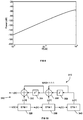
- a classical signal processing technique 10 for performing rational sample rate conversion includes two processing blocks 12 , 16 and a digital lowpass filter 14 connected between the two blocks 12 , 16 .
- the rational sample rate conversion is performed by interpolating the signal data x[n] by an integer L in block 12 and decimating it by an integer M in block 16 to form the output y[m].
- the digital lowpass filter 14 has a frequency cutoff that is driven by the function max[L,M].
- the classical technique 10 for performing rational sample rate conversion provides conversion by any rational factor of L/M.
- This technique 10 has several shortcomings. While polyphase implementations may work to keep the computational effort low, a large L/M ratio can drive up coefficient storage and processing requirements, which is undesirable. Moreover, a programmable L/M ratio can complicate the hardware implementation of the technique 10 . Additionally, sampling rates cannot be changed smoothly over time, and the implementation may not be convenient for managing variable group delay, among other things.
- a system for digital signal processing may include an instrument configured to process signal data by controlling and or changing the sampling rate of the signal data.
- the dual-modulus counter may comprise a Multi-stAge noise Shaping Digital Delta-Sigma Modulator (MASH DDSM).
- MASH DDSM Multi-stAge noise Shaping Digital Delta-Sigma Modulator
- FIG. 1 illustrates a classical signal processing re-sampling technique
- FIG. 2 is a block diagram illustration of an example of analog signal resampling, which in the ideal sense represents the Whittaker-Shannon interpolation technique;
- FIG. 3 is a simplified block diagram showing an example instrument for processing signal data in accordance with the disclosed principles
- FIG. 4 is a simplified block diagram of logic for performing a re-sampling process that may be utilized by the instrument of FIG. 3 in accordance with the disclosed principles;
- FIG. 5 is a simplified block diagram of an example timing controller that may be used in the re-sampling implementation of FIG. 4 in accordance with the disclosed principles;
- FIG. 6 is a simplified block diagram of an example of the timing control logic and an example of a Multi-stAge noise Shaping Digital Delta-Sigma Modulator (MASH DDSM) that may be used in the re-sampling logic of FIG. 4 in accordance with the disclosed principles;
- MASH DDSM Multi-stAge noise Shaping Digital Delta-Sigma Modulator
- FIG. 7 illustrates a diagrammatic representation of an example error feedback modulator (EFM) that may be used in the MASH DDSM of FIG. 6 in accordance with the disclosed principles;
- EFM error feedback modulator
- FIG. 8 illustrates a diagrammatic representation of an example linearized EFM that may be used in the analysis of the MASH DDSM of FIG. 6 in accordance with the disclosed principles
- FIG. 9 is an illustrative graph of noise power spectral density of an EFM of the MASH DDSM of FIG. 6 in accordance with the disclosed principles.
- FIG. 10 illustrates a diagrammatic representation of an example of the MASH DDSM of FIG. 6 in accordance with the disclosed principles.
- the technique 20 may include an ideal DAC (Digital-to-Analog Converter) 22 , a perfect lowpass filter 24 , and an ideal ADC (Analog-to-Digital Converter) 26 .
- the input signal x[nT] is used as an input to the DAC 22
- the output of the DAC 22 is used as an input to the lowpass filter 24 whose output is used as an input by the ADC 26 .
- the output of the ADC 26 is interpolated output y[m T′].
- the Whittaker-Shannon interpolation approach 20 can be visualized as reconstructing a bandlimited signal from the ideal DAC 22 using the perfect lowpass filter 24 and then resampling the signal at the new sample period T′ with the ideal ADC 26 .
- the ideal lowpass filter 24 perfectly bandlimits the sample sequence, x[nT], to the region
- the filter kernel i.e., the well-known sinc function
- the kernel must have infinite support, but to make the problem tractable, the kernel must be replaced with one having finite support. This is typically done by windowing the sinc function accordingly (e.g., by a Lanczos algorithm, Kaiser window, etc.).
- the Lanczos reconstruction kernel, h(t) is reproduced below:
- h ⁇ ( t ) ⁇ sin ⁇ ⁇ c ⁇ ( t ) ⁇ ⁇ sin ⁇ ⁇ c ⁇ ( t k ) - k ⁇ t ⁇ k 0 otherwise
- the instrument 100 may input signals and or waveforms having a first sample rate, which is different than the sample rate of the instrument 100 (e.g., because the signals may have been produced and or captured by a device having one or more sample rates different than the sample rate of the instrument 100 ).
- the instrument 100 may be configured to resample the input signal and process the signal with the sample rate of the instrument 100 .
- the resampling may occur in real-time or in an offline manner and sampling rates may be changed smoothly over time in accordance with the disclosed principles.
- the instrument 100 includes a controller 110 connected to a plurality of I/O ports 112 and to a user interface 126 .
- the controller 110 includes a Field Programmable Gate Array (FPGA) 116 (discussed in more detail below) and a storage device such as, for example, a memory 118 .
- the memory 118 may be configured to store recorded signal data and other data that may be accessed and or output by the FPGA 116 .
- the controller 110 may include other circuitry such as, for example, a microprocessor, processor, an application-specific integrated circuit (ASIC), ADC, and or a DAC.
- the I/O ports 112 include an Ethernet port 120 , a universal serial bus (USB) port 122 , and a connector 124 for receiving an antenna (not shown).
- the I/O ports 112 permit the instrument 100 to transmit and receive signal and other data.
- the I/O ports 112 may connect to a source of the signal data, which could be another device outputting real-time signal data or a storage device when the instrument 100 is used in an offline (i.e., non-real-time) manner. It should be appreciated that in other embodiments the instrument 100 may include other ports capable of transmitting and receiving data.
- the instrument 100 also includes the user interface 126 , which may be operated by the user to control the operation of the instrument 100 .
- the user interface 126 may include a display and keyboard. It should be appreciated that in other embodiments the instrument 100 may be configured to be connected to peripherals such as a display monitor, keyboard, and mouse to permit a user to control the operation of the instrument 100 .
- the instrument 100 may be configured to process signal data that may include a number of different waveforms, and in many instances each waveform may have a different sample rate from that of the instrument 100 . As described in greater detail below, the instrument 100 may be configured to resample the waveform's sample rate to the instrument's cardinal sample rate. To do so, the instrument 100 has logic that utilizes a windowed-sinc filter based on the following equation:
- the output sample (y) at time index m is constructed from the convolution of 2*k input samples with kernel values corresponding to the appropriate time index.
- the instrument 100 may be configured to interpolate the filter kernel value (i.e., the windowed sinc function value) according to the time index from a lookup table of kernel values.
- the interpolation used by instrument 100 may be linear interpolation. It should be appreciated, however, that other interpolation strategies (cubic, quadratic, Farrow-type) may be used in other embodiments. Generally, higher order interpolation trades fewer kernel values in the lookup table for greater computational effort.
- FIG. 4 is a block diagram illustrates an example of the logic 200 that may be used by the instrument 100 to implement the resampling process performed in accordance with the disclosed principles.
- the resampling process, and hence the logic 200 illustrated in FIG. 4 may utilize a form of interpolation to process signal data as described below in more detail.
- the logic 200 is implemented in the FPGA 116 .
- the logic 200 may include a shaping filter implemented as a windowed-sinc filter 210 and a timing controller 280 for controlling the windowed-sinc filter 210 .
- the windowed-sinc filter 210 includes a switch 212 controlled by a “valid” signal output from the timing controller 280 . When the resampling filter requires a new input sample the valid signal momentarily closes the switch 212 .
- the switch 212 When in the closed position, the switch 212 connects the input signal x[n] to a delay line structure composed of a series of registers 214 , 216 , 218 and also to a first multiplier 220 .
- Each register 214 , 216 , 218 may introduce a one timing sample delay to the data it inputs. It should be appreciated that the length of the filter (and by extension the delay line, multipliers, adders, etc.) can be arbitrarily large, as indicated by the ellipses in the figures.
- the output of register 214 is input into register 216 .
- the output of register 216 is input into register 218 .
- each register 214 , 216 , 218 is used as an input to a respectively connected multiplier 222 , 224 , 226 .
- the multipliers 220 , 222 , 224 , 226 each receive another input signal, shown as coefficients c 0 [m], c 1 [m], c 2 [m], c 2k ⁇ 1 [m] (explained below in more detail).
- the outputs of the multipliers 220 , 222 , 224 , 226 are summed together through a series of adders 228 , 230 , 232 .
- the output of adder 232 is the resampled waveform output signal y[m].
- multipliers 234 , 238 , 242 , 246 use the time residual (“time_residual”) signal output from the timing controller 280 as one of their inputs.
- the memories 250 , 252 , 254 , 256 , 258 , 260 , 262 , 264 are read only memories (ROMs).
- memories 250 , 254 , 258 , 262 may respectively store the difference values kernel_diff 0 [addr], kernel_diff 1 [addr], kernel_diff 2 [addr], kernel_diff 2k ⁇ 1 [addr] while memories 252 , 256 , 260 , 264 may respectively store the kernel values kernel 0 [addr], kernel 1 [addr], kernel 2 [addr], kernel 2k ⁇ 1 [addr].
- the memories 250 , 252 , 254 , 256 , 258 , 260 , 262 , 264 are indexed by the “address” signal output from the timing controller 280 .
- the outputs of memories 250 , 254 , 258 , 262 e.g., difference values kernel_diff 0 [addr], kernel_diff 1 [addr], kernel_diff 2 [addr], kernel_diff 2k ⁇ l [addr]
- multipliers 234 , 238 , 242 , 246 are used as inputs by multipliers 234 , 238 , 242 , 246 , respectively.
- the outputs of memories 252 , 256 , 260 , 264 are used as inputs by adders 236 , 240 , 244 , 248 .
- coefficient c 0 [m] may be generated via linear interpolation by adding the output of multiplier 234 (e.g., time_residual*kernel_diff 0 [addr]) to the memory 252 output (e.g., kernel 0 [addr]) at adder 236
- coefficient c 01 [m] may be generated by adding the output of multiplier 238 (e.g., time_residual*kernel_diff 1 [addr]) to the memory 256 output (e.g., kernel 1 [addr]) at adder 240
- coefficient c 2 [m] may be generated by adding the output of multiplier 242 (e.g., time_residual*kernel_diff 2 [addr]) to the memory 260 output (e.g., kernel 2 [addr]) at adder 244 and coefficient c 2k ⁇ 1 [m] may be generated by adding the output of multiplier 246 (e.g.,
- the windowed-sinc filter 210 may be controlled by the timing controller 280 that produces the “valid”, “address,” and “time_residual” signals (discussed above) from a counter that represents the current sample time.
- the timing controller 280 also referred to herein as timing control or timing state machine
- the counter 282 may be implemented as an error feedback modulator (i.e., modulo-2 W ) having a first input (x) for receiving an integer N and a second input (y) for receiving a feedback signal from the register 286 .
- the carry bit (c) of the counter 282 may be used as the “valid” signal because it indicates the rollover of the time value and the acceptance of a new sample into the windowed-sinc filter 210 .
- the splitter 284 contains logic to split the counter 282 output (x+y) into the “address” signal and “time_residual” signal discussed above.
- the M-most significant bits from the counter 282 output (x+y) form the “address” that is used as an index into the kernel memories 250 , 252 , 254 , 256 , 258 , 260 , 262 , 264 ( FIG. 4 ) for each zero-crossing.
- the W-M least significant bits from the counter 282 output (x+y) form the “time_residual” signal and represent the residue from the ideal kernel time value and the stored kernel value such that time_residual for output sample m for resample rate p is given by m*p ⁇ floor(m*p).
- the aforementioned logic 200 can achieve an arbitrary amount of interpolation accuracy with a sufficiently large time counter register width, W.
- the actual interpolation rate error cannot be made identically zero for rates that cannot be expressed exactly as a ratio of N/2 W .
- this may not be an issue as the length of the waveform may be small enough that sub-hertz interpolation rate errors are not significant.
- the interpolation rate error may accumulate, causing increasing errors in time accuracy.
- the logic 200 may be improved upon to further the disclosed principles.
- the time counter increments by N for B-A cycles, then counts by N+1 for A cycles, which may yield an average increment value of N+A/B.
- One potential drawback of this approach is that aliased frequency content may appear at multiples of A/B from the output frequency. Accordingly, in one or more embodiments, the dual-modulus action of the time counter may be “dithered” to break-up the spurious content and spread it out over frequency.
- the logic of the FPGA 116 may utilize a Multi-stAge noise Shaping Digital Delta-Sigma Modulator (MASH DDSM) 310 , as shown in FIG. 6 , to break-up the spurious content and spread it out over frequency in accordance with the disclosed principles.
- MASH DDSM 310 is included in a novel timing state machine or timing control logic 300 that outputs “valid,” “address” and “time_residual” signals that may be used to control windowed-sinc filter 210 ( FIG. 4 ).
- the MASH DDSM 310 includes a plurality of error feedback modulators (EFMs) 320 , 330 , 340 connected to a noise shaping network 350 .
- the first EFM 320 has a modulo-B accumulator 322 and a register 324 .
- the modulo-B accumulator 322 has an input (x) connected to receive the A signal and a second input (y) connected to receive a feedback signal w 1 [n] from the register 324 .
- the register 324 inputs e 1 [n] from the modulo-B accumulator 322 output (x+y) and introduces a one sample delay forming feedback signal w 1 [n].
- the second EFM 330 has a modulo-B accumulator 332 and a register 334 .
- the modulo-B accumulator 332 has an input (x) connected to receive e 1 [n] from the modulo-B accumulator 322 output (x+y) and a second input (y) connected to receive a feedback signal w 2 [n] from the register 334 .
- the register 334 inputs e 2 [n] from the modulo-B accumulator 332 output (x+y) and introduces a one sample delay forming feedback signal w 2 [n].
- the third EFM 340 has a modulo-B accumulator 342 and a register 344 .
- the modulo-B accumulator 342 has an input (x) connected to receive e 2 [n] from the modulo-B accumulator 332 output (x+y) and a second input (y) connected to receive a feedback signal w 3 [n] from the register 344 .
- the register 344 inputs e 3 [n] from the modulo-B accumulator 342 output (x+y) and introduces a one sample delay forming feedback signal w 3 [n].
- the carry bits y 1 [n], y 2 [n], y 3 [n] output from the carry bit (c) portion of EFMs 320 , 330 , 340 are output to the noise shaping network 350 .
- the noise shaping network 350 comprises two adders 352 , 356 and two registers 354 , 358 .
- the first adder 352 may input the carry bit y 1 [n] from the first EFM 320 and the second adder 356 may input the carry bit y 2 [n] from the second EFM 330 and the second register 358 may input the carry bit y 3 [n] from the third EFM 340 .
- the output of the second register 358 which is a delayed carry bit y 3 [n] is added to the carry bit y 2 [n] from the second EFM 330 and the carry bit y 3 [n] from the third EFM 330 at adder 356 .
- the output of adder 356 is input by register 354 .
- the output of register 354 which is a delayed summation from adder 356 , is added to the carry bit y 1 [n] from the first EFM 320 and the summation from adder 356 at adder 352 .
- the output of adder 352 is the A/B signal, which has an instantaneous value that varies according to the order of the MASH DDSM, but whose average value over time corresponds to the ratio A/B and is used as an input by adder 302 .
- the output of adder 302 which may be N+A/B is used as an input (x) of the accumulator 282 of timing controller 280 .
- FIG. 7 illustrates a first order EFM model 420 comprising two adders 422 , 426 , feedback/delay register 424 and processing blocks 428 , 430 .
- the input x[n] is added to a feedback signal w[n] at adder 422 .
- the output v[n] of adder 422 is input at block 428 whose output y[n] is the output of the EFM 420 .
- the output y[n] is fed into block 430 whose output is input by a negative terminal of adder 426 .
- Adder 426 also inputs the output v[n] from adder 422 to create output e[n] that is fed to the register 424 that outputs the feedback signal w[n] to adder 422 .
- the following variables may be computed during the process:
- FIG. 8 illustrates a linearized first order EFM model 520 comprising three adders 522 , 526 , 532 , feedback/delay register 524 and processing blocks 528 , 530 .
- the input x[n] is added to a feedback signal w[n] at adder 522 .
- the output v[n] of adder 522 is input at block 528 whose output is fed to adder 532 .
- the other input of adder 532 receives the quantization noise e c [n].
- the output adder 532 is the output y[n] of the EFM 520 .
- the output y[n] is fed into block 530 whose output is input by a negative terminal of adder 526 .
- Adder 526 also inputs the output v[n] from adder 522 to create output e[n] that is fed to the register 524 that outputs the feedback signal w[n] to adder 522 .
- the non-linear modulus operator, Q( ⁇ ), of the EFM 520 is absorbed as quantization noise, e q [n].
- the average output of the carry signal, y[n] is the value x[n]/B.
- the error feedback modulators 320 . 330 , 340 of the MASH DDSM 310 are cascaded, with outputs that are fed into the noise shaping network 350 .
- the noise shaping network 350 consists of cascaded differentiators which possess a transfer function with a highpass response. The differentiators perfectly cancel the quantization noise of the previous EFM. The noise is shaped by the highpass response of the differentiator network, resulting in the noise spectral density being minimized at 0 Hz and increasing towards the Nyquist frequency. This result is displayed by the graph shown in FIG. 9 .
- the theory of operation of a MASH DDSM may be explained by first analyzing the operation of the 1st order Error Feedback Modulator (EFM) 420 , shown in FIG. 7 .
- the 1st order EFM consists of a digital accumulator with modulus B, input x[n], registered state w[n], and output y[n] (the carry out bit of the accumulator).
- the output of the EFM 420 is given by:
- Y ⁇ [ z ] X ⁇ [ z ] B + E q ⁇ [ z ] ⁇ ( 1 - z - 1 ) .
- a MASH DDSM 310 network consists of several cascaded EFM 420 .
- the accumulator output signal, e[n], of each EFM is fed to the subsequent EFM.
- the carry output signal, y[n], of each EFM is fed to a noise shaping network.
- the cascade of three 1st order EFMs with noise shaping network (MASH 1-1-1 DDSM 310 ) is illustrated in FIG. 10 .
- the noise shaping network consists of a cascade of digital differentiators. The differentiators of FIG. 10 cancel the noise of the intermediate EFM error signal, e 1 [n] and shape the quantization noise of the final EFM according to a highpass response:
- the MASH DDSM 310 may be a 1-1-1 MASH DDSM and may include three 1st order EFMs 320 , 330 , 340 whose respective outputs y 1 [n], y 2 [n], y 3 [n] are fed to the nose shaping network 350 .
- the non-linear modulus operator, Q( ), of the modulo-B accumulators can be assumed to quantization noise with a uniform spectral density.
- the quantization noise e 1 [n] from the first EFM 320 is input into the second EFM 330 whose quantization noise e 2 [n] is input into the third EFM 340 .
- Register 358 inputs the output y 3 [n] and delays it by one time sample before it output to adder 356 .
- Adder 356 also inputs the original output y 3 [n].
- the output of adder 356 (y 2 [n]+y 3 [n]+delayed y 3 [n]) is input at register 354 , which delays it by one time sample, and outputs the delayed result to adder 352 .
- Adder 352 adds the output y1[n] from EFM 320 , the original output from adder 356 and the delayed output from adder 356 (via register 354 ) to form the output y[n].
- the inclusion of the MASH DDSM 310 to the time counter integer component overcomes any restriction of perfect rate interpolation for those rates expressible as a ratio of the counter modulus. Any potential MASH DDSM noise is pushed out to the Nyquist frequency and is naturally attenuated by the filter lowpass response. Additionally, the MASH DDSM provides shaped dither noise that improves spurious generation in the filter response as a result of coefficient quantization.
- the modulus (B) of the MASH DDSM in accordance with the disclosed principles may be programmable to any value up to the maximum MASH accumulator counter width, expanding further the achievable interpolation rates.
- the MASH DDSM implementation is only one approach for adding shaped noise for the purpose of time-variant filtering.
- Shaped noise is typically realized via delta-sigma modulation, of which the MASH implementation is one, but not exclusive, means of generating the sequence.
- other methods of intentionally adding noise to a filter implementation which is at a low level and shaped to be rejected by the filtering action itself, may be used to improve resampling and processing of the signal data.
Landscapes
- Engineering & Computer Science (AREA)
- Theoretical Computer Science (AREA)
- Physics & Mathematics (AREA)
- General Engineering & Computer Science (AREA)
- General Physics & Mathematics (AREA)
- Computer Hardware Design (AREA)
- Mathematical Physics (AREA)
- Compression, Expansion, Code Conversion, And Decoders (AREA)
Abstract
Description
The windowing length typically coincides with the kth zero-crossing of the sinc function (sinc(0)=1, sinc(n)=0 for all other n integers).
The output sample (y) at time index m is constructed from the convolution of 2*k input samples with kernel values corresponding to the appropriate time index. With a windowed sinc function, the number of required filter coefficients scales with the interpolation ratio, p, and the
kernel_diff[addr]=kernel[addr+1]−kernel[addr], where addr=[0:2M−1]
c g[m]=time_residual*kernel_diffg[addr]+kernelg[addr], where g=[0:2k−1].
p=[N+A/B]/2W
N=floor(p*2W)
A=[f in*2W −N*f out]/Q
B=f out /Q
Q=GCD[f out ,f in*2W −N*f out]
where:
fin is the baseband sample rate of the target waveform,
fout is the sample rate of the instrument 100 (e.g., 250 MHz), and
W is a constant (e.g., 32).
w[n+1]=(x[n]+w[n])mod B
The output of the
The non-linear modulus operator Q(⋅) 428 of the modulo-B accumulator can be linearized by the approximation:
where eq[n] is quantization with a uniform spectral density. The linearized 1st
e[n]=v[n]−B·y[n]=—B·e q[n],
Subsequently, the output y[n] of the
which has the z-transform equivalent of:
Claims (16)
Priority Applications (2)
| Application Number | Priority Date | Filing Date | Title |
|---|---|---|---|
| US16/720,852 US10972121B2 (en) | 2018-12-20 | 2019-12-19 | System and method for signal resampling |
| US17/215,534 US11329664B2 (en) | 2018-12-20 | 2021-03-29 | System and method for signal resampling |
Applications Claiming Priority (2)
| Application Number | Priority Date | Filing Date | Title |
|---|---|---|---|
| US201862782481P | 2018-12-20 | 2018-12-20 | |
| US16/720,852 US10972121B2 (en) | 2018-12-20 | 2019-12-19 | System and method for signal resampling |
Related Child Applications (1)
| Application Number | Title | Priority Date | Filing Date |
|---|---|---|---|
| US17/215,534 Continuation US11329664B2 (en) | 2018-12-20 | 2021-03-29 | System and method for signal resampling |
Publications (2)
| Publication Number | Publication Date |
|---|---|
| US20200204192A1 US20200204192A1 (en) | 2020-06-25 |
| US10972121B2 true US10972121B2 (en) | 2021-04-06 |
Family
ID=71097034
Family Applications (2)
| Application Number | Title | Priority Date | Filing Date |
|---|---|---|---|
| US16/720,852 Active US10972121B2 (en) | 2018-12-20 | 2019-12-19 | System and method for signal resampling |
| US17/215,534 Active US11329664B2 (en) | 2018-12-20 | 2021-03-29 | System and method for signal resampling |
Family Applications After (1)
| Application Number | Title | Priority Date | Filing Date |
|---|---|---|---|
| US17/215,534 Active US11329664B2 (en) | 2018-12-20 | 2021-03-29 | System and method for signal resampling |
Country Status (4)
| Country | Link |
|---|---|
| US (2) | US10972121B2 (en) |
| JP (1) | JP7572952B2 (en) |
| DE (1) | DE112019006377T5 (en) |
| WO (1) | WO2020132239A1 (en) |
Families Citing this family (2)
| Publication number | Priority date | Publication date | Assignee | Title |
|---|---|---|---|---|
| GB201611083D0 (en) * | 2016-06-24 | 2016-08-10 | Dialog Semiconductor Bv | Digital sample rate conversion |
| GB2620920B (en) * | 2022-07-21 | 2024-09-25 | Advanced Risc Mach Ltd | System, devices and/or processes for application of kernel coefficients |
Citations (3)
| Publication number | Priority date | Publication date | Assignee | Title |
|---|---|---|---|---|
| US4775851A (en) * | 1987-06-01 | 1988-10-04 | Motorola, Inc. | Multiplierless decimating low-pass filter for a noise-shaping A/D converter |
| US6035182A (en) * | 1998-01-20 | 2000-03-07 | Motorola, Inc. | Single counter dual modulus frequency division apparatus |
| US20080167564A1 (en) * | 2007-01-10 | 2008-07-10 | Starr Life Sciences Corp. | Techniques for accurately deriving physiologic parameters of a subject from photoplethysmographic measurements |
Family Cites Families (10)
| Publication number | Priority date | Publication date | Assignee | Title |
|---|---|---|---|---|
| US4053739A (en) * | 1976-08-11 | 1977-10-11 | Motorola, Inc. | Dual modulus programmable counter |
| GB2116081A (en) | 1982-02-26 | 1983-09-21 | Gen Electric | Inserts for cutting tools |
| US6208671B1 (en) * | 1998-01-20 | 2001-03-27 | Cirrus Logic, Inc. | Asynchronous sample rate converter |
| DE60131115T2 (en) * | 2000-06-02 | 2008-08-14 | Texas Instruments Inc., Dallas | Sample rate converter and method |
| KR100398048B1 (en) | 2001-12-11 | 2003-09-19 | 한국전자통신연구원 | Structure of a delta-sigma fractional divider |
| US7024171B2 (en) | 2003-02-25 | 2006-04-04 | Icom America, Incorporated | Fractional-N frequency synthesizer with cascaded sigma-delta converters |
| DE102004006995B4 (en) | 2004-02-12 | 2007-05-31 | Infineon Technologies Ag | Digital phase-locked loop for sub-μ technologies |
| CN101213752B (en) | 2005-07-04 | 2011-03-30 | 松下电器产业株式会社 | Semiconductor device and radio circuit device using same |
| US9082389B2 (en) | 2012-03-30 | 2015-07-14 | Apple Inc. | Pre-shaping series filter for active noise cancellation adaptive filter |
| US9225349B2 (en) * | 2013-08-20 | 2015-12-29 | Skyworks Solutions, Inc. | Dither-less multi-stage noise shaping fractional-N frequency synthesizer systems and methods |
-
2019
- 2019-12-19 US US16/720,852 patent/US10972121B2/en active Active
- 2019-12-19 WO PCT/US2019/067465 patent/WO2020132239A1/en not_active Ceased
- 2019-12-19 DE DE112019006377.4T patent/DE112019006377T5/en active Pending
- 2019-12-19 JP JP2021534394A patent/JP7572952B2/en active Active
-
2021
- 2021-03-29 US US17/215,534 patent/US11329664B2/en active Active
Patent Citations (3)
| Publication number | Priority date | Publication date | Assignee | Title |
|---|---|---|---|---|
| US4775851A (en) * | 1987-06-01 | 1988-10-04 | Motorola, Inc. | Multiplierless decimating low-pass filter for a noise-shaping A/D converter |
| US6035182A (en) * | 1998-01-20 | 2000-03-07 | Motorola, Inc. | Single counter dual modulus frequency division apparatus |
| US20080167564A1 (en) * | 2007-01-10 | 2008-07-10 | Starr Life Sciences Corp. | Techniques for accurately deriving physiologic parameters of a subject from photoplethysmographic measurements |
Also Published As
| Publication number | Publication date |
|---|---|
| US11329664B2 (en) | 2022-05-10 |
| US20210218412A1 (en) | 2021-07-15 |
| JP7572952B2 (en) | 2024-10-24 |
| WO2020132239A1 (en) | 2020-06-25 |
| US20200204192A1 (en) | 2020-06-25 |
| JP2022515060A (en) | 2022-02-17 |
| DE112019006377T5 (en) | 2021-09-02 |
Similar Documents
| Publication | Publication Date | Title |
|---|---|---|
| EP0887937B1 (en) | Preventing overload of a quantiser in analogue and digital converters | |
| US7719446B2 (en) | Method and apparatus for computing interpolation factors in sample rate conversion systems | |
| US8369973B2 (en) | Efficient asynchronous sample rate conversion | |
| EP0837561B1 (en) | Sampling frequency converting apparatus | |
| JPH0642619B2 (en) | Interpolative time-discrete filter device | |
| US7227477B2 (en) | Method and apparatus for performing sample rate conversion | |
| US11329664B2 (en) | System and method for signal resampling | |
| US7619546B2 (en) | Asynchronous sample rate conversion using a digital simulation of an analog filter | |
| JPH1117498A (en) | Sampling rate converting unit, its device and its method | |
| Pei et al. | Fractional bilinear transform for analog-to-digital conversion | |
| US6411238B1 (en) | Digital to analog converter with step voltage generator for smoothing analog output | |
| US9954514B2 (en) | Output range for interpolation architectures employing a cascaded integrator-comb (CIC) filter with a multiplier | |
| JPS62500554A (en) | Analog-digital converter | |
| US7324025B1 (en) | Non-integer interpolation using cascaded integrator-comb filter | |
| US6515608B1 (en) | Digital-analog converter and method, and data interpolation device and method | |
| US6763407B1 (en) | Digital-to-analog converter with plural voltage holding sections, plural step function generators, voltage summing section and integrator | |
| US20140139280A1 (en) | Systems, apparatus, and methods for providing continuous-time signal differentiation and integration | |
| US10498312B2 (en) | Glitch immune cascaded integrator comb architecture for higher order signal interpolation | |
| US9876490B2 (en) | Systems, apparatus, and methods for providing continuous-time signal differentiation and integration | |
| US20230198506A1 (en) | Arbitrary sample rate conversion using modulus accumulator | |
| JPH04192711A (en) | Sampling frequency converter | |
| JPH0640616B2 (en) | Digital filter-frequency characteristic converter | |
| Xiao et al. | An algorithm for selecting sampling rate in arbitrary waveform generator | |
| CN120454680A (en) | A method and device for generating fractional time parameters in a Farrow structure filter | |
| JP2005203932A (en) | Sampling rate conversion kernel |
Legal Events
| Date | Code | Title | Description |
|---|---|---|---|
| AS | Assignment |
Owner name: VIAVI SOLUTIONS INC., CALIFORNIA Free format text: ASSIGNMENT OF ASSIGNORS INTEREST;ASSIGNOR:HAMLIN, SEAN;REEL/FRAME:051335/0195 Effective date: 20191218 |
|
| FEPP | Fee payment procedure |
Free format text: ENTITY STATUS SET TO UNDISCOUNTED (ORIGINAL EVENT CODE: BIG.); ENTITY STATUS OF PATENT OWNER: LARGE ENTITY |
|
| STPP | Information on status: patent application and granting procedure in general |
Free format text: DOCKETED NEW CASE - READY FOR EXAMINATION |
|
| STPP | Information on status: patent application and granting procedure in general |
Free format text: NON FINAL ACTION MAILED |
|
| STPP | Information on status: patent application and granting procedure in general |
Free format text: NOTICE OF ALLOWANCE MAILED -- APPLICATION RECEIVED IN OFFICE OF PUBLICATIONS |
|
| STPP | Information on status: patent application and granting procedure in general |
Free format text: PUBLICATIONS -- ISSUE FEE PAYMENT RECEIVED |
|
| STPP | Information on status: patent application and granting procedure in general |
Free format text: PUBLICATIONS -- ISSUE FEE PAYMENT VERIFIED |
|
| STCF | Information on status: patent grant |
Free format text: PATENTED CASE |
|
| MAFP | Maintenance fee payment |
Free format text: PAYMENT OF MAINTENANCE FEE, 4TH YEAR, LARGE ENTITY (ORIGINAL EVENT CODE: M1551); ENTITY STATUS OF PATENT OWNER: LARGE ENTITY Year of fee payment: 4 |