US10970361B2 - Information processing apparatus, ising device, and information processing apparatus control method - Google Patents
Information processing apparatus, ising device, and information processing apparatus control method Download PDFInfo
- Publication number
- US10970361B2 US10970361B2 US15/615,868 US201715615868A US10970361B2 US 10970361 B2 US10970361 B2 US 10970361B2 US 201715615868 A US201715615868 A US 201715615868A US 10970361 B2 US10970361 B2 US 10970361B2
- Authority
- US
- United States
- Prior art keywords
- value
- neuron
- sum
- values
- circuit
- Prior art date
- Legal status (The legal status is an assumption and is not a legal conclusion. Google has not performed a legal analysis and makes no representation as to the accuracy of the status listed.)
- Expired - Fee Related, expires
Links
Images


Classifications
-
- G—PHYSICS
- G06—COMPUTING OR CALCULATING; COUNTING
- G06F—ELECTRIC DIGITAL DATA PROCESSING
- G06F17/00—Digital computing or data processing equipment or methods, specially adapted for specific functions
- G06F17/10—Complex mathematical operations
- G06F17/11—Complex mathematical operations for solving equations, e.g. nonlinear equations, general mathematical optimization problems
-
- G—PHYSICS
- G06—COMPUTING OR CALCULATING; COUNTING
- G06F—ELECTRIC DIGITAL DATA PROCESSING
- G06F13/00—Interconnection of, or transfer of information or other signals between, memories, input/output devices or central processing units
- G06F13/14—Handling requests for interconnection or transfer
- G06F13/20—Handling requests for interconnection or transfer for access to input/output bus
-
- G—PHYSICS
- G06—COMPUTING OR CALCULATING; COUNTING
- G06F—ELECTRIC DIGITAL DATA PROCESSING
- G06F30/00—Computer-aided design [CAD]
- G06F30/20—Design optimisation, verification or simulation
-
- G—PHYSICS
- G06—COMPUTING OR CALCULATING; COUNTING
- G06F—ELECTRIC DIGITAL DATA PROCESSING
- G06F7/00—Methods or arrangements for processing data by operating upon the order or content of the data handled
- G06F7/58—Random or pseudo-random number generators
- G06F7/588—Random number generators, i.e. based on natural stochastic processes
-
- G—PHYSICS
- G06—COMPUTING OR CALCULATING; COUNTING
- G06N—COMPUTING ARRANGEMENTS BASED ON SPECIFIC COMPUTATIONAL MODELS
- G06N3/00—Computing arrangements based on biological models
- G06N3/02—Neural networks
- G06N3/04—Architecture, e.g. interconnection topology
- G06N3/044—Recurrent networks, e.g. Hopfield networks
-
- G06N3/0445—
-
- G—PHYSICS
- G06—COMPUTING OR CALCULATING; COUNTING
- G06N—COMPUTING ARRANGEMENTS BASED ON SPECIFIC COMPUTATIONAL MODELS
- G06N3/00—Computing arrangements based on biological models
- G06N3/02—Neural networks
- G06N3/04—Architecture, e.g. interconnection topology
- G06N3/047—Probabilistic or stochastic networks
-
- G06N3/0472—
-
- G—PHYSICS
- G06—COMPUTING OR CALCULATING; COUNTING
- G06N—COMPUTING ARRANGEMENTS BASED ON SPECIFIC COMPUTATIONAL MODELS
- G06N3/00—Computing arrangements based on biological models
- G06N3/02—Neural networks
- G06N3/06—Physical realisation, i.e. hardware implementation of neural networks, neurons or parts of neurons
- G06N3/063—Physical realisation, i.e. hardware implementation of neural networks, neurons or parts of neurons using electronic means
-
- G06N5/003—
-
- G—PHYSICS
- G06—COMPUTING OR CALCULATING; COUNTING
- G06N—COMPUTING ARRANGEMENTS BASED ON SPECIFIC COMPUTATIONAL MODELS
- G06N5/00—Computing arrangements using knowledge-based models
- G06N5/01—Dynamic search techniques; Heuristics; Dynamic trees; Branch-and-bound
-
- G06N7/005—
-
- G—PHYSICS
- G06—COMPUTING OR CALCULATING; COUNTING
- G06N—COMPUTING ARRANGEMENTS BASED ON SPECIFIC COMPUTATIONAL MODELS
- G06N7/00—Computing arrangements based on specific mathematical models
- G06N7/01—Probabilistic graphical models, e.g. probabilistic networks
-
- G—PHYSICS
- G06—COMPUTING OR CALCULATING; COUNTING
- G06N—COMPUTING ARRANGEMENTS BASED ON SPECIFIC COMPUTATIONAL MODELS
- G06N7/00—Computing arrangements based on specific mathematical models
- G06N7/02—Computing arrangements based on specific mathematical models using fuzzy logic
- G06N7/04—Physical realisation
- G06N7/046—Implementation by means of a neural network
Definitions
- the embodiments discussed herein relate to an information processing apparatus, an ising device, and an information processing apparatus control method.
- Neumann computers are not very suitable for solving multivariable optimization problems.
- an ising device also referred to as a Boltzmann machine
- Such an ising device performs calculation by replacing a problem to be calculated with an ising model, which is a model representing the behavior of a ferromagnetic spin.
- An ising device can be modeled by using a neural network.
- each of the units (bits) included in the ising device functions as a neuron that outputs 0 or 1 on the basis of states of the other bits and weight values (also referred to as coupling coefficients) each of which indicates coupling strength between the corresponding bit and one of the other bits.
- the ising device performs simulated annealing to obtain, as a solution, a combination of bit states from which a minimum value of the above energy function (also referred to as a cost function, an objective function, etc.) is obtained.
- a conventional ising device uses an energy function (which will hereinafter be referred to as a second-order energy function) including a weight value of coupling strength between two bits.
- an energy function which will hereinafter be referred to as a high-order energy function
- weight values indicating mutual coupling strength among three or more bits.
- ancillary bit has conventionally been introduced. Addition of this ancillary bit could slow down the convergence into an optimal solution or decrease the number of usable bits in simulated annealing.
- an information processing apparatus including: an ising device; and a control device, wherein the ising device includes: a random signal generation circuit that outputs, a plurality of times, a selection signal for randomly selecting a first neuron whose output value is allowed to be updated from n neurons, wherein n is a natural number of 3 or more, d ⁇ 1 arithmetic circuits that calculate, based on a plurality of weight values indicating strength of 2-body coupling to d-body coupling of two to d neurons including the first neuron selected from the n neurons based on the selection signal and n-bit output values of the n neurons, d ⁇ 1 energy values indicating energies generated by the respective 2-body to d-body coupling or change amounts of the d ⁇ 1 energy values, wherein d is a natural number not less than 3 and not more than n, an adder circuit that calculates a first sum by adding up the d ⁇ 1 energy values or calculates a second sum by adding up the change amounts of
- FIG. 1 illustrates an example of an information processing apparatus according to a first embodiment
- FIG. 2 illustrates an example of an arithmetic circuit that calculates a local field value generated by d-body coupling
- FIG. 3 illustrates examples of an update circuit and a holding circuit
- FIG. 4 illustrates an example of an ising device in which an optimization problem using a third-order energy function is mapped
- FIG. 5 illustrates an example of an arithmetic circuit that calculates a local field value generated by 2-body coupling
- FIG. 6 illustrates an example of an arithmetic circuit that calculates a local field value generated by 3-body coupling
- FIG. 7 is a flowchart illustrating an example of an operation of the information processing apparatus
- FIG. 8 is a flowchart illustrating an example of simulated annealing
- FIG. 9 illustrates progress of simulated annealing
- FIG. 10 illustrates examples of weight values indicating 2-body coupling
- FIG. 11 illustrates examples of weight values indicating 3-body coupling
- FIG. 12 illustrates examples of weight values indicating 3-body coupling when the number of neurons is n
- FIG. 13 illustrates examples of weight values indicating 4-body coupling when the number of neurons is n
- FIG. 14 is a flowchart illustrating an example of weight value list generation processing
- FIG. 15 illustrates an example of a weight value list
- FIG. 16 illustrates an example of an information processing apparatus according to a second embodiment
- FIG. 17 illustrates an example of a circuit unit
- FIG. 18 illustrates an example of an arithmetic circuit that calculates a change amount of a local field value generated by 2-body coupling
- FIG. 19 illustrates an example of an arithmetic circuit that calculates a change amount of a local field value generated by 3-body coupling
- FIG. 20 illustrates an example of a two-output-value selector circuit
- FIG. 21 is a flowchart illustrating an example of simulated annealing performed by the information processing apparatus according to the second embodiment.
- FIG. 1 illustrates an example of an information processing apparatus 1 according to a first embodiment.
- the information processing apparatus 1 includes an ising device 2 , a control device 3 , and a memory 4 .
- the control device 3 maps an optimization problem using a high-order (d ⁇ 3) energy function in the ising device 2 .
- the ising device 2 according to the first embodiment functions as a neural network including n neurons (n is a natural number of 3 or more).
- the ising device 2 includes a random signal generation circuit 10 , arithmetic circuits 11 a 1 to 11 a (d ⁇ 1), an adder circuit 12 , a comparator circuit 13 , an update circuit 14 , a holding circuit 15 , a bias value holding circuit 16 , and a noise generation circuit 17 .
- the ising device 2 is realized by a single semiconductor integrated circuit (a single chip).
- the random signal generation circuit 10 outputs a selection signal for randomly selecting a neuron whose output value is allowed to be updated from the n neurons a plurality of times. For example, each of the n neurons is given a different identification number (which will hereinafter be referred to as a neuron ID).
- the random signal generation circuit 10 outputs a selection signal that specifies i (1 ⁇ i ⁇ n) as a neuron ID.
- the random signal generation circuit 10 includes linear feedback shift registers (LFSRs).
- the d ⁇ 1 arithmetic circuits 11 a 1 to 11 a (d ⁇ 1) receive the selection signal outputted by the random signal generation circuit 10 and n-bit output values x 1 to x n of the n neurons outputted by the holding circuit 15 .
- the arithmetic circuit 11 a 1 to 11 a (d ⁇ 1) calculate d ⁇ 1 energy values h i2 to h id on the basis of a plurality of weight values indicating strength of 2-body coupling to d-body coupling of two to d neurons including the neuron selected by the selection signal and the output values x 1 to x n .
- the energy values will hereinafter be referred to as local field values.
- the local field values h i2 to h id indicate energies generated by the respective 2-body coupling to d-body coupling.
- the control device 3 sets these weight values indicating strength of 2-body coupling to d-body coupling (which will simply be referred to as weight values indicating 2-body coupling to d-body coupling) on the basis of the problem to be calculated and stores the weight values in storage units (for example, registers) in the arithmetic circuit 11 a 1 to 11 a (d ⁇ 1).
- the weight value of 2-body coupling of neurons 20 and 21 whose neuron IDs are i and k, respectively, is denoted by W ik .
- the weight value of 2-body coupling of the neuron 21 and a neuron 22 whose neuron IDs are k and j, respectively, is denoted by W jk .
- the weight value of 2-body coupling of the neurons 20 and 22 whose neuron IDs are i and j, respectively, is denoted by W ij .
- the weight value of 3-body coupling of the neurons 20 to 22 whose neuron IDs are i, j, and k, respectively, is denoted by W ijk .
- the weight value of 4-body coupling of the neurons 20 to 22 and a neuron 23 whose neuron IDs are j, k, and l, respectively, is denoted by W ijkl .
- the adder circuit 12 adds up the local field values h i2 to h id and outputs a sum of these values.
- the comparator circuit 13 adds up the sum obtained by the adder circuit 12 , a noise value, and a bias value and compares a sum of these values with a threshold (for example, 0). On the basis of the comparison result, the comparator circuit 13 determines and outputs the output value of the neuron selected by the selection signal.
- the comparator circuit 13 includes an adder circuit that adds up the sum obtained by the adder circuit 12 , the noise value, and the bias value.
- a value (energy value) obtained by adding up the sum obtained by the adder circuit 12 and the bias value will be referred to as a local field value h i .
- the comparator circuit 13 when the sum of the local field value h i and the noise value is negative, the comparator circuit 13 outputs 1. When the sum of the local field value h i and the noise value is positive, the comparator circuit 13 outputs 0.
- the bias value may be 0.
- the update circuit 14 outputs n-bit updated output values of the n neurons in which one bit has been updated on the basis of the selection signal and the output value outputted by the comparator circuit 13 . For example, when the output value of a neuron whose neuron ID is i outputted by the comparator circuit 13 is different from the previous value, the update circuit 14 outputs n-bit updated output values in which the i-th bit has been updated. When the output value of the neuron whose neuron ID is i outputted by the comparator circuit 13 is the same as the previous value, the update circuit 14 may output no updated output values.
- the holding circuit 15 holds the updated output values outputted by the update circuit 14 and outputs the updated output values as the n-bit output values of the n neurons used by the arithmetic circuits 11 a 1 to 11 a (d ⁇ 1) in synchronization with a clock signal clk.
- the holding circuit 15 is realized by a plurality of flip flops, for example.
- the clock signal clk is supplied by the control device 3 , for example.
- the clock signal clk may be supplied by a clock signal generation circuit (not illustrated) arranged outside or inside the ising device 2 .
- the bias value holding circuit 16 is a register or a flash memory and holds a bias value for each of the n neurons.
- the bias value holding circuit 16 supplies the bias value of a neuron specified by the selection signal outputted by the random signal generation circuit 10 to the comparator circuit 13 , for example.
- the control device 3 sets the bias values in advance on the basis of the problem to be calculated.
- the noise generation circuit 17 outputs a noise value for performing simulated annealing on the basis of an instruction from the control device 3 .
- the noise generation circuit 17 may also be configured by using LFSRs.
- the noise generation circuit 17 includes an amplifier circuit.
- the control device 3 changes the amplification factor of the amplifier circuit, to control the amplitude of the noise value.
- the control device 3 controls the random signal generation circuit 10 and the noise generation circuit 17 to control the noise width. For example, to perform simulated annealing, the control device 3 controls the amplifier circuit included in the noise generation circuit 17 and gradually drops the noise width of the noise value (the amplitude of the noise). In addition, the control device 3 previously sets a plurality of weight values and a plurality of bias values on the basis of the optimization problem to be calculated. In addition, the control device 3 performs mapping by writing the plurality of weight values in registers in the arithmetic circuits 11 a 1 to 11 a (d ⁇ 1) via buses (not illustrated) and writing the plurality of bias values in the bias value holding circuit 16 .
- control device 3 may be realized by a processor.
- the processor include a central processing unit (CPU), a micro processing unit (MPU), a digital signal processor (DSP), an application specific integrated circuit (ASIC), and a programmable logic device (PLD).
- the processor may be a combination of at least two of a CPU, an MPU, a DSP, an ASIC, and a PLD.
- the control device 3 may be a personal computer (PC), a server computer, or the like.
- the memory 4 is a non-volatile storage device that holds an operating system (OS), middleware, software programs such as application software programs, and data executed by the processor.
- OS operating system
- middleware software programs
- the memory 4 may hold a program for generating weight value lists, which will be described below.
- the non-volatile storage device include a flash memory, a solid state drive (SSD), and a hard disk drive (HDD).
- the above information processing apparatus 1 realizes operations of the ising energy function by using hardware modules.
- a high-order energy function E(x) is defined by the following expression (1).
- the first term on the right side of expression (1) is directed to all the combinations of two neurons selectable from all the neurons without missing any neuron or redundantly counting any neuron. More specifically, the first term represents the sum of products, each of which is obtained by multiplying the output values of two neurons and a weight value of the corresponding 2-body coupling by each other.
- the second term on the right side of expression (1) represents the sum of products, each of which is obtained by multiplying the bias value by the output value per neuron.
- b i represents the bias value of the neuron whose neuron ID is i.
- the third term on the right side of expression (1) is directed to all the combinations of three neurons selectable from all the neurons without missing any neuron or redundantly counting any neuron.
- the third term represents the sum of products, each of which is obtained by multiplying the output values of three neurons and a weight value of the corresponding 3-body coupling by each other.
- the fourth term on the right side of expression (1) is directed to all the combinations of four neurons selectable from all the neurons without missing any neuron or redundantly counting any neuron. More specifically, the fourth term represents the sum of products, each of which is obtained by multiplying the output values of four neurons and a weight value of the corresponding 4-body coupling by each other.
- the change of the energy value when the output value of a neuron changes from 1 to 0 or from 0 to 1 is determined by the weight values, each of which indicates coupling between the neuron and one of the other neurons, and the output values of the neurons.
- h i b i + ⁇ j ⁇ W ij ⁇ x j + ⁇ ⁇ j , k ⁇ ⁇ W ijk ⁇ x j ⁇ x k + ⁇ ⁇ j , k , l ⁇ ⁇ W ijkl ⁇ x j ⁇ x k ⁇ x l + ... ( 3 )
- the second term on the right side of expression (3) represents the energy generated by 2-body coupling of neurons including the neuron whose neuron ID is i.
- the third term on the right side represents the energy generated by 3-body coupling of neurons including the neuron whose neuron ID is i.
- W ijk is a weight value of 3-body coupling of neurons whose neuron IDs are i, j, and k, respectively, of all the n neurons.
- the fourth term on the right side represents the energy generated by 4-body coupling of neurons including the neuron whose neuron ID is i.
- W ijkl is a weight value of 4-body coupling of neurons whose neuron IDs are i, j, k, and l, respectively, of all the n neurons.
- the arithmetic circuits 11 a 1 to 11 a (d ⁇ 1) illustrated in FIG. 1 calculate the local field value h i2 to h id that indicate the energies generated by the respective 2-body coupling to d-body coupling.
- the arithmetic circuit 11 a 1 calculates the local field value h i2 corresponding to the second term on the right side of expression (3), and the arithmetic circuit 11 a 2 calculates the local field value h i3 corresponding to the third term of expression (3).
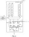
- FIG. 2 illustrates an example of an arithmetic circuit that calculates a local field value generated by d-body coupling.
- the arithmetic circuit 11 a (d ⁇ 1) includes registers 30 a 1 to 30 an , a selector circuit 31 , a multiplier unit 32 , and an adder unit 33 .
- the registers 30 a 1 to 30 an hold a plurality of weight values of d-body coupling of d neurons.
- the register 30 a 1 holds a plurality of weight values of d-body coupling of the d neurons including a neuron whose neuron ID is 1.
- the register 30 a 2 holds a plurality of weight values of d-body coupling of the d neurons including a neuron whose neuron ID is 2.
- the register 30 an holds a plurality of weight values of d-body coupling of the d neurons including a neuron whose neuron ID is n.
- the selector circuit 31 outputs a plurality of weight values stored in one of the registers 30 a 1 to 30 an on the basis of the selection signal outputted by the random signal generation circuit 10 . For example, when the selector circuit 31 receives a selection signal that specifies the neuron whose neuron ID is 1, the selector circuit 31 outputs a plurality of weight values stored in the register 30 a 1 .
- the multiplier unit 32 and the adder unit 33 calculate the energy (the local field value h id ) generated by d-body coupling, the energy being a part of the local field value h i expressed by the expression (3), on the basis of the output values x 1 to x n and the plurality of weight values outputted by the selector circuit 31 .
- the multiplier unit 32 includes m multiplier circuits 32 a 1 to 32 am
- the adder unit 33 includes p adder circuits 33 a 1 to 33 ap .
- the number of multiplier circuits 32 a 1 to 32 am and the number of adder circuits 33 a 1 to 33 ap will be described below.
- FIG. 3 illustrates examples of the update circuit 14 and the holding circuit 15 .
- the update circuit 14 includes a multiplexer 14 a and selector circuits 14 b 1 to 14 bn .
- the holding circuit 15 includes flip flops 15 a 1 to 15 an.
- the multiplexer 14 a generates a selection signal supplied to the selector circuit 14 b 1 to 14 bn on the basis of the selection signal outputted by the random signal generation circuit 10 . For example, when the multiplexer 14 a receives a selection signal for selecting one of the n neurons, the multiplexer 14 a supplies 1 as a selection signal to one of the selector circuits 14 b 1 to 14 bn that corresponds to the selected neuron. The multiplexer 14 a supplies 0 to the other selector circuits.
- the multiplexer 14 a when the multiplexer 14 a receives a selection signal that specifies the neuron whose neuron ID is 1, the multiplexer 14 a supplies 1 as the selection signal to the selector circuit 14 b 1 and supplies 0 as the selection signal to the selector circuits 14 b 2 to 14 bn.
- the n selector circuits 14 b 1 to 14 bn are arranged to correspond to the n neurons.
- Each of the selector circuits 14 b 1 to 14 bn has two input terminals. One of the input terminals of a selector circuit is connected to the output terminal of a corresponding one of the flip flops 15 a 1 to 15 an , and the other input terminal is connected to the output terminal of the comparator circuit 13 .
- this selector circuit selects and outputs the output value of the neuron outputted by the comparator circuit 13 .
- this selector circuit selects and outputs a value outputted by the corresponding one of the flip flops 15 a 1 to 15 an.
- the flip flops 15 a 1 to 15 an in the holding circuit 15 captures and outputs the values (n-bit updated output values) outputted by the selector circuits 14 b 1 to 14 bn in synchronization with the clock signal clk.
- the selector circuit 14 b 1 selects and outputs the output value of the neuron outputted by the comparator circuit 13 .
- the selector circuits 14 b 2 to 14 bn select and output the values outputted by the respective flip flops 15 a 2 to 15 an .
- the holding circuit 15 outputs n-bit output values in which only the bit value corresponding to the neuron whose neuron ID is 1 has been updated.
- FIG. 4 illustrates an example of an ising device 2 a in which an optimization problem using a third-order energy function is mapped.
- like reference characters refer to like elements.
- the ising device 2 a in which an optimization problem using a third-order energy function is mapped includes the two arithmetic circuits 11 a 1 and 11 a 2 .
- the arithmetic circuit 11 a 1 calculates the local field value h i2 , which is the energy generated by 2-body coupling of two neurons including the neuron whose neuron ID is i.
- the arithmetic circuit 11 a 2 calculates the local field value h i3 , which is the energy generated by 3-body coupling of three neurons including the neuron whose neuron ID is i.
- An adder circuit 12 a outputs a sum of the two local field values h i2 and h i3 .
- FIG. 5 illustrates an example of the arithmetic circuit 11 a 1 that calculates a local field value generated by 2-body coupling.
- the arithmetic circuit 11 a 1 includes registers 40 a 1 to 40 an , a selector circuit 41 , a multiplier unit 42 , and an adder unit 43 .
- the registers 40 a 1 to 40 an hold a plurality of weight values, each of which indicates 2-body coupling of two neurons.
- the register 40 a 1 holds weight values W 12 to W 1n , each of which indicates 2-body coupling of two neurons including the neuron whose neuron ID is 1.
- the register 40 a 2 holds a plurality of weight values W 21 and W 23 to W 2n each of which indicates 2-body coupling of two neurons including the neuron whose neuron ID is 2.
- the register 40 an holds weight values W n1 to W n(n-1) , each of which indicates 2-body coupling of two neurons including a neuron whose neuron ID is n.
- the selector circuit 41 outputs a plurality of weight values stored in one of the registers 40 a 1 to 40 an on the basis of the selection signal outputted by the random signal generation circuit 10 .
- the multiplier unit 42 includes n multiplier circuits 42 a 1 to 42 an , and the adder unit 43 includes q adder circuits 43 a 1 to 43 aq .
- the multiplier unit 42 and the adder unit 43 calculate the energy (the local field value h i2 ) generated by 2-body coupling, the energy being a part of the local field value h i expressed by the expression (3), on the basis of the output values x 1 to x n and the plurality of weight values outputted by the selector circuit 41 .
- FIG. 6 illustrates an example of the arithmetic circuit 11 a 2 that calculates a local field value generated by 3-body coupling.
- the arithmetic circuit 11 a 2 includes registers 50 a 1 to 50 an , a selector circuit 51 , a multiplier unit 52 , and an adder unit 53 .
- the register 50 a 1 to 50 an hold a plurality of weight values, each of which indicates 3-body coupling of three neurons.
- the register 50 a 1 holds weight values W 121 , W 131 , W 132 , . . . , and W 1n(n-1) , each of which indicates 3-body coupling of three neurons including the neuron whose neuron ID is 1.
- the register 50 a 2 holds a plurality of weight values W 221 , W 231 , W 232 , . . . , and W 2n(n-1) , each of which indicates 3-body coupling of three neurons including the neuron whose neuron ID is 2.
- the register 50 holds weight values W n21 , W n31 , W n32 , . . . , and W nn(n-1) , each of which indicates 3-body coupling of three neurons including the neuron whose neuron ID is n.
- the selector circuit 51 outputs a plurality of weight values stored in one of the registers 50 a 1 to 50 an on the basis of the selection signal outputted by the random signal generation circuit 10 .
- the multiplier unit 52 includes r multiplier circuits 52 a 1 to 52 ar
- the adder unit 53 includes s adder circuits 53 a 1 to 53 as .
- the multiplier unit 52 and the adder unit 53 calculate the energy (the local field value h i3 ) generated by 3-body coupling, the energy being a part of the local field value h i expressed by the expression (3), on the basis of the output values x 1 to x n and the plurality of weight values outputted by the selector circuit 51 .
- FIG. 7 is a flowchart illustrating an example of an operation of the information processing apparatus 1 .
- control device 3 extracts the weight values of 2-body coupling to d-body coupling stored in the memory 4 , for example (step S 1 ).
- This example assumes that the weight values based on the problem to be calculated are prepared in advance.
- control device 3 writes the extracted weight values in registers in arithmetic circuits 11 a 1 to 11 a (d ⁇ 1) (for example, in the registers 30 a 1 to 30 an in the case of the arithmetic circuit 11 a (d ⁇ 1)) (step S 2 ). Namely, in step S 2 , the optimization problem is mapped. In step S 2 , the control device 3 may write the bias value of an individual neuron in the bias value holding circuit 16 .
- step S 3 the control device 3 acquires the output values x 1 to x n of the n neurons as a result of the simulated annealing. Namely, the control device 3 acquires the output values x 1 to x n as a solution to the optimization problem (step S 4 ). Next, the control device 3 ends the present processing.
- FIG. 8 is a flowchart illustrating an example of simulated annealing.
- the random signal generation circuit 10 outputs a selection signal for randomly selecting a neuron whose output value is allowed to be updated (a neuron whose neuron ID is i) (step S 10 ).
- the arithmetic circuit 11 a 1 to 11 a calculate the local field values h i2 to h id that indicate the energies generated by 2-body coupling to d-body coupling, respectively (step S 11 ).
- the adder circuit calculates a sum of the local field values h i2 to h id (step S 12 ).
- step S 13 When a sum of the local field value h i (a sum of the sum calculated by the adder circuit 12 and a bias value) and a noise value is smaller than a threshold (for example, 0) (step S 13 : YES), the comparator circuit 13 outputs 1 as its output value (new_x i ) (step S 14 ).
- a threshold for example, 0
- step S 13 When a sum of the local field value h i and the noise value is equal to or more than the threshold (step S 13 : NO), the comparator circuit 13 outputs 0 as its output value (new_x i ) (step S 15 ).
- step S 16 After steps S 14 or S 15 , if the output value new_x i differs from the original output value x i of the neuron whose neuron ID is i (step S 16 : NO), the update circuit 14 outputs n-bit updated output values in which the i-th bit has been updated (step S 17 ). Next, the processing returns to step S 10 .
- step S 16 determines whether the output value new_x i is the same as the original output value x i (step S 16 : YES). If the output value new_x i is the same as the original output value x i (step S 16 : YES), the control device 3 determines whether the output values x 1 to x n (neuron states) have remained the same for a certain period (step S 18 ). If the output values x 1 to x n have remained the same for a certain period (step S 18 : YES), the control device 3 ends the simulated annealing.
- step S 18 If the output values x 1 to x n have changed within the certain period (step S 18 : NO), the processing returns to step S 10 .
- the simulated annealing is performed as the noise generation circuit 17 gradually drops the noise width under control of the control device 3 every time a neuron allowed to be updated is selected.
- the noise generation circuit 17 generates a noise value so that the probability with which the output value of the comparator circuit 13 represents 1 accords with a sigmoid function.
- the noise generation circuit 17 generates a noise value so that a probability P i (h i ) with which the output value x i of the neuron whose neuron ID is i represents 1 satisfies the following expression (4).
- P i ( h i ) 1/[1+exp( ⁇ h i /T )] (4)
- T represents an effective temperature
- a probability density function p(ns) of a noise value ns generated to obtain the probability P i (h i ) in expression (4) is expressed by the following expression (5).
- p ( ns ) exp( ⁇ h i /T )/[1+exp( ⁇ h i /T )] 2 (5)
- FIG. 9 illustrates progress of simulated annealing.
- FIG. 9 illustrates how the convergence into a solution is achieved as the noise width is dropped from W 1 to W 3 . Dropping the noise width means dropping the effective temperature T in expression (5).
- the arithmetic circuits 11 a 1 to 11 a calculate the energies (the local field values h i2 to h id ) generated by 2-body coupling to d-body coupling of 2 to d neurons, respectively.
- a value based on a sum of the local field values h i2 to h id is compared with a threshold, and the output values of the neurons are determined on the basis of the comparison result.
- an optimization problem using a high-order energy function does not need to be converted into an optimization problem using a plurality of second-order energy functions, an optimization problem is easily mapped in the ising device 2 .
- Examples of such an optimization problem using a high-order energy function include a non-deterministic polynomial (NP) complete problem.
- NP non-deterministic polynomial
- FIG. 10 illustrates examples of weight values indicating 2-body coupling.
- FIG. 10 illustrates a weight value group 60 a including a plurality of weight values each of which indicates 2-body coupling when the number of neurons is 4.
- W 21 is a weight value that indicates 2-body coupling of the two neurons whose neuron IDs are 2 and 1, respectively.
- W 21 W 12
- W 31 W 13
- W 41 W 14
- W 42 W 24
- W 43 W 34
- each of the weight values W 11 , W 22 , W 33 , and W 44 in a weight value group 60 b in FIG. 10 is 0.
- calculation may be performed without the weight values W 11 , W 22 , W 33 , and W 44 .
- both weight values having a symmetry relationship such as W 21 and W 12 are used to calculate the local field value h i2 generated by 2-body coupling, as illustrated in FIG. 5 .
- FIG. 11 illustrates examples of weight values indicating 3-body coupling.
- FIG. 11 illustrates a weight value group 61 a including a plurality of weight values each of which indicates 3-body coupling of three neurons including the neuron whose neuron ID is 2 when the number of neurons is 4.
- W 231 is a weight value that indicates 3-body coupling of the three neurons whose neuron IDs are 2, 3, and 1, respectively.
- the ising device 2 or 2 a when the ising device 2 or 2 a according to the present embodiment calculates a local field value h 23 generated by 3-body coupling that includes the neuron whose neuron ID is 2, the ising device 2 or 2 a uses the weight values in a triangular domain 61 e in FIG. 11 (six weight values in the example in FIG. 11 ).
- FIG. 12 illustrates examples of weight values indicating 3-body coupling when the number of neurons is n.
- FIG. 12 illustrates weight value groups 65 a 1 , 65 a 2 , . . . , and 65 an including weight values W ijk (i, j, and k are each a natural number not less than 1 and not more than n) each of which indicates 3-body coupling.
- the weight value group 65 a 1 includes weight values W 1jk in which i is 1
- the weight value group 65 a 2 includes weight values W 2jk in which i is 2
- the weight value group 65 an includes weight values W njk in which i is n.
- the ising device 2 or 2 a uses only the weight values in triangular domains 65 b 1 , 65 b 2 , . . . , and 65 bn in the weight value groups 65 a 1 to 65 an .
- the weight value group 65 a 1 of all the weight values arranged in a matrix in FIG. 12 , a plurality of weight values on a diagonal line (for example, weight values W 111 , W 122 , . . . , and W 1nn ) and a plurality of weight values arranged under the diagonal line are not used.
- the number of weight values included in each of the triangular domains 65 b 1 to 65 bn is expressed as Nw by expression (6).
- Nw n 2 - n 2 ( 6 )
- the value Nw is obtained by subtracting the number (n) of weight values on the above diagonal line from the number (n ⁇ n) of weight values included in one of the weight value groups 65 a 1 to 65 an and dividing the obtained value by half. Namely, when calculating the local field value h i3 , the ising device 2 or 2 a uses Nw weight values per i.
- FIG. 13 illustrates examples of weight values indicating 4-body coupling when the number of neurons is n.
- FIG. 13 illustrates weight value groups 66 a 1 , 66 a 2 , . . . , 66 an , 67 a 1 , . . . , and 67 an including weight values W ijkl (i, j, k, and l are each a natural number not less than 1 and not more than n) each of which indicates 4-body coupling.
- the weight value group 66 a 1 includes weight values W 11kl in which i and j are each 1, and the weight value group 66 a 2 includes weight values W 12kl in which i and j are 1 and 2, respectively, and the weight value group 66 an includes weight values W lnkl in which i is 1 and j is n.
- the weight value groups 67 a 1 to 67 an include weight values W 21kl to W 2nkl in which i is 2 and j is one of 1 to n.
- the ising device 2 uses only the weight values included in triangular domains 66 b 1 , 66 b 2 , 66 bn , 67 b 1 , . . . , and 67 bn in the weight value groups 66 a 1 to 66 an and 67 a 1 to 67 an .
- the number of weight values included in each of the triangular domains 66 b 1 to 66 bn and 67 b 1 to 67 bn is expressed as Nw by the above expression (6).
- the ising device 2 uses (n ⁇ Nw) weight values generated by 4-body coupling per i.
- n d - 3 ⁇ Nw n d - 3 ⁇ n 2 - n 2 ( 7 )
- control device 3 On the basis of the above contents, the control device 3 generates weight value lists to be written in registers in the arithmetic circuits 11 a 1 to 11 a (d ⁇ 1) in the following procedure, for example.
- FIG. 14 is a flowchart illustrating an example of weight value list generation processing.
- control device 3 sets a variable curr_d to 2 (step S 20 ).
- control device 3 determines whether the variable curr_d is 2 (step S 21 ).
- the control device 3 determines a size S of an individual weight value list to be n, which is the same as the number of neurons (step S 22 ).
- the size S may be n ⁇ 1.
- step S 22 the control device 3 generates weight value lists having the size S for 2-body coupling (step S 23 ).
- the control device 3 generates n weight value lists having the size S.
- the generated weight value lists are stored in the memory 4 , for example.
- control device 3 extracts the weight values, each of which indicates 2-body coupling of two neurons including the neuron whose neuron ID is i, from the 2-body-coupling weight value group stored in the memory 4 and copies the extracted weight values in the i-th weight value list of the n weight value lists (step S 24 ).
- the control device 3 performs this processing per i.
- the control device 3 copies the weight values W 12 , W 13 , and W 14 , each of which indicates 2-body coupling of two neurons including the neuron whose neuron ID is 1, from the weight value group 60 a as illustrated in FIG. 10 to the first weight value list.
- the control device 3 copies the weight values W 21 , W 23 , and W 24 , each of which indicates 2-body coupling of two neurons including the neuron whose neuron ID is 2, from the weight value group 60 a to the second weight value list.
- control device 3 copies the weight values W 31 , W 32 , and W 34 , each of which indicates 2-body coupling of two neurons including the neuron whose neuron ID is 3, from the weight value group 60 a to the third weight value list.
- control device 3 copies the weight values W 41 , W 42 , and W 43 , each of which indicates 2-body coupling of two neurons including the neuron whose neuron ID is 4, from the weight value group 60 a to the fourth weight value list.
- step S 21 when the variable curr_d is not 2 (step S 21 : NO), the control device 3 calculates a size S of an individual weight value list on the basis of expression (7) (step S 25 ).
- step S 25 the control device 3 generates weight value lists having the size S for curr_d-body coupling (step S 26 ).
- the control device 3 generates n weight value lists having the size S for curr_d-body coupling.
- the generated weight value lists are stored in the memory 4 , for example.
- control device 3 extracts the weight values, each of which indicates curr_d-body coupling of curr_d neurons including the neuron whose neuron ID is i, from the curr_d-body-coupling weight value groups and copies the extracted weight values in the i-th weight value lists (step S 27 ).
- the control device 3 copies only a plurality of weight values, such as those that are included in the triangular domains 66 b 1 to 66 bn illustrated in FIG. 13 .
- the control device 3 performs this processing per i.
- FIG. 15 illustrates an example of a weight value list.
- the weight values W 1121 to W 1nn(n-1) are included in the triangular domain 66 b 1 illustrated in FIG. 13 and the number of weight values W 1121 to W 11n(n-1) is Nw.
- the other weight values in the weight value list 70 are included in the triangular domains 66 b 2 to 66 bn illustrated in FIG. 13 .
- the weight value list 70 includes n ⁇ Nw weight values.
- step S 24 or S 27 in FIG. 14 the control device 3 increments the variable curr_d (step S 28 ) and determines whether curr_d d (step S 29 ).
- step S 29 YES
- step S 29 : NO the control device 3 ends the weight value list generation processing.
- the weight value lists may be transmitted from an apparatus other than the information processing apparatus 1 via a network to the information processing apparatus 1 , and the transmitted weight value lists may be stored in the memory 4 .
- this source apparatus include a client apparatus such as a client computer operated by a user and a server apparatus such as a server computer.
- the control device 3 writes the weight values included in the above weight value lists in registers in the arithmetic circuits 11 a 1 to 11 a (d ⁇ 1) illustrated in FIG. 1 , for example.
- the number of weight values written in an individual one of the registers 30 a 1 to 30 an is a number expressed by the above expression (7).
- the number of weight values written in an individual one of the registers 30 a 1 to 30 an is limited by a number expressed by expression (7).
- increase of the size of the registers 30 a 1 to 30 an is prevented.
- increase of the number m of the multiplier circuits 32 a 1 to 32 am in the multiplier unit 32 and the number p of the adder circuits 33 a 1 to 33 ap in the adder unit 33 that calculate a local field value by using the weight values is also prevented.
- the number m of the multiplier circuits 32 a 1 to 32 am is expressed by expression (8).
- m ( d ⁇ 1) ⁇ n d ⁇ 3 ⁇ Nw (8)
- FIG. 16 illustrates an example of an information processing apparatus 80 according to a second embodiment.
- like reference characters refer to like elements.
- the information processing apparatus 80 includes an ising device 81 including circuit units 81 a 1 to 81 a 4 and an update control circuit 81 b.
- Each of the circuit units 81 a 1 to 81 a 4 corresponds to a single neuron.
- a circuit that performs processing on the basis of an algorithm called “DeGloria algorithm” may be used as an individual one of the circuit units 81 a 1 to 81 a 4 .
- the number of circuit units 81 a 1 to 81 a 4 is 4, assuming that the number n of neurons is 4.
- a different number of circuit units may be used depending on the number n of neurons used.
- Each of the circuit units 81 a 1 to 81 a 4 calculates the above local field value h i (1 ⁇ i ⁇ 4) on the basis of the weight values indicating 2-body to d-body coupling and 4-bit output values x 1 , x 2 , x 3 , and x 4 of the four neurons.
- each of the circuit units 81 a 1 to 81 a 4 outputs 0 or 1 as one of the output values x 1 to x 4 on the basis of the result of a comparison between a sum of the local field value h i and a noise value and a threshold (for example, 0).
- Each of the circuit units 81 a 1 to 81 a 4 performs the following processing on the basis of a DeGloria algorithm when calculating the local field value h i .
- the neurons connected to this neuron perform addition or subtraction of the change amount caused by the updating on the original local field value h i .
- the circuit units 81 a 1 to 81 a 4 calculate the change amounts of the d ⁇ 1 local field values indicating the energies generated by 2-body to d-body coupling, respectively, on the basis of the weight values indicating 2-body to d-body coupling, the output values x 1 to x 4 , and a signal udn.
- the signal udn indicates the neuron ID of a neuron whose output value has been updated.
- each of the circuit units 81 a 1 to 81 a 4 calculates a sum of the change amounts of the d ⁇ 1 local field values.
- each of the circuit units 81 a 1 to 81 a 4 reverses the plus or minus of the sum on the basis of a signal uds, which is the updated output value of one of the neurons, and adds the reserved sum to the original sum. In this way, the original sum is updated.
- This updated sum corresponds to the local field value h i .
- each of the circuit units 81 a 1 to 81 a 4 has a function of holding a comparison result (output value) and a function of outputting one of the signals ud 1 to ud 4 , which is set to 1 when the previous output value held differs from the current output value.
- the update control circuit 81 b operates under control of the control device 3 .
- the update control circuit 81 b receives the output values x 1 to x 4 and the signals ud 1 to ud 4 from the circuit units 81 a 1 to 81 a 4 and outputs the signal udn indicating the neuron ID of the neuron whose output value has been updated, the signal uds indicating the updated output value, and the output values x 1 to x 4 .
- FIG. 17 illustrates an example of a circuit unit.
- the circuit units 81 a 2 to 81 a 4 are configured in the same way.
- the circuit unit 81 a 1 includes arithmetic circuits 82 and 83 , an adder circuit 84 , a selector circuit 85 , a multiplier circuit 86 , an adder circuit 87 , a register 88 , an adder circuit 89 , a comparator circuit 90 , an XOR circuit 91 , and a register 92 .
- the arithmetic circuit 82 calculates a change amount ⁇ h 12 of a local field value generated by 2-body coupling of two neurons including a neuron whose neuron ID is 1.
- the change amount ⁇ h 12 when the output value of a neuron whose neuron ID is 3 is updated is expressed by expression (10).
- the arithmetic circuit 82 when calculating the change amount ⁇ h 12 of the local field value generated by 2-body coupling, the arithmetic circuit 82 does not need the output values x 1 to x 4 .
- the arithmetic circuit 83 calculates a change amount ⁇ h 13 of a local field value generated by 3-body coupling of three neurons including the neuron whose neuron ID is 1.
- the change amount ⁇ h 13 when the output value of the neuron whose neuron ID is 3 is updated is expressed by expression (11).
- the arithmetic circuit 82 uses two of the output values x 1 to x 4 .
- the arithmetic circuits 82 and 83 may be realized by the following circuits.
- FIG. 18 illustrates an example of the arithmetic circuit 82 that calculates a change amount of a local field value generated by 2-body coupling.
- the arithmetic circuit 82 includes a register 82 a and a selector circuit 82 b.
- the register 82 a holds weight values W 12 to W 14 , each of which indicates 2-body coupling of two neurons including the neuron whose neuron ID is 1.
- the control device 3 writes the weight values W 12 to W 14 in the register 82 a in accordance with the above processing.
- the selector circuit 82 b selects one of the weight values W 12 to W 14 on the basis of the signal udn and outputs the selected weight value as the change amount ⁇ h 12 of the local field value. For example, when the selector circuit 82 b receives a signal udn indicating that the output value of the neuron whose neuron ID is 3 has been updated, since the change amount ⁇ h 12 is expressed by expression (10), the selector circuit 82 b selects and outputs the weight value W 13 . When the selector circuit 82 b receives a signal udn indicating that the output value of the neuron whose neuron ID is 2 has been updated, the selector circuit 82 b selects and outputs the weight value W 12 . When the selector circuit 82 b receives a signal udn indicating that the output value of the neuron whose neuron ID is 4, the selector circuit 82 b selects and outputs the weight value W 14 .
- FIG. 19 illustrates an example of the arithmetic circuit 83 that calculates a change amount of a local field value generated by 3-body coupling.
- the arithmetic circuit 83 includes a register 83 a , selector circuits 83 b and 83 c , a 2-output-value selector circuit 83 d , multiplier circuits 83 e and 83 f , and an adder circuit 83 g.
- the register 83 a holds weight values W 123 , W 124 , and W 134 , each of which indicates 3-body coupling of three neurons including the neuron whose neuron ID is 1.
- the control device 3 writes the weight values W 123 to W 134 in the register 83 a in accordance with the above processing.
- the selector circuit 83 b selects one of the weight values W 123 to W 134 on the basis of the signal udn and outputs the selected weight value.
- the selector circuit 83 c also selects one of the weight values W 123 to W 134 on the basis of the signal udn and outputs the selected weight value.
- the selector circuits 83 b and 83 c when the selector circuits 83 b and 83 c receive a signal udn indicating that the output value of the neuron whose neuron ID is 3 has been updated, since the change amount ⁇ h 13 is expressed by expression (11), the selector circuits 83 b and 83 c select and output the weight values W 123 and W 134 , respectively.
- the selector circuits 83 b and 83 c receive a signal udn indicating that the output value of the neuron whose neuron ID is 2 has been updated, the selector circuits 83 b and 83 c select and output the weight values W 123 and W 124 , respectively.
- the selector circuits 83 b and 83 c When the selector circuits 83 b and 83 c receive a signal udn indicating that the output value of the neuron whose neuron ID is 4, the selector circuits 83 b and 83 c select and output the weight values W 124 and W 134 , respectively.
- the 2-output-value selector circuit 83 d selects two of the output values x 1 to x 4 on the basis of the signal udn and outputs the selected output value.
- the 2-output-value selector circuit 83 d is realized by the following circuit, for example.
- FIG. 20 illustrates an example of the 2-output-value selector circuit 83 d.
- the 2-output-value selector circuit 83 d includes registers 100 to 102 , a selector circuit 103 , and a register 104 .
- the register 100 holds the output values x 2 and x 3 and outputs the output values x 2 and x 3 as 2-bit signals.
- the register 101 holds the output values x 2 and x 4 and outputs the output values x 2 and x 4 as 2-bit signals.
- the register 102 holds the output values x 3 and x 4 and outputs the output values x 3 and x 4 as 2-bit signals.
- the selector circuit 103 selects the signals outputted from one of the registers 100 to 102 on the basis of the signal udn and outputs the selected signals.
- the selector circuit 103 selects and outputs the 2-bit signals outputted from the register 100 .
- the selector circuit 103 receives a signal udn indicating that the output value of the neuron whose neuron ID is 3 has been updated, the selector circuit 103 selects and outputs the 2-bit signals outputted from the register 101 .
- the selector circuit 103 receives a signal udn indicating that the output value of the neuron whose neuron ID is 2 has been updated, the selector circuit 103 selects and outputs the 2-bit signals outputted from the register 102 .
- the register 104 holds the 2-bit signals outputted by the selector circuit 103 and outputs these signals in parallel.
- the output value x 1 is not illustrated in FIG. 20 .
- the multiplier circuit 83 e in FIG. 19 outputs a product of the weight value outputted by the selector circuit 83 b and one of the output values x 2 to x 4 outputted by the 2-output-value selector circuit 83 d .
- the selector circuit 83 b and the 2-output-value selector circuit 83 d receive a signal udn indicating that the output value of the neuron whose neuron ID is 3 has been updated, since the change amount ⁇ h 13 is expressed by expression (11), the multiplier circuit 83 e outputs a product of the weight value W 123 and the output value x 2 .
- the multiplier circuit 83 f outputs a product of the weight value outputted by the selector circuit 83 c and one of the output values x 2 to x 4 outputted by the 2-output-value selector circuit 83 d .
- the selector circuit 83 c and the 2-output-value selector circuit 83 d receive a signal udn indicating that the output value of the neuron whose neuron ID is 3 has been updated, since the change amount ⁇ h 13 is expressed by expression (11), the multiplier circuit 83 f outputs a product of the weight value W 134 and the output value x 4 .
- the adder circuit 83 g calculates a sum of the output values of the multiplier circuits 83 e and 83 f and outputs the sum as the change amount ⁇ h 13 .
- the adder circuit 84 calculates a sum of the change amounts ⁇ h 12 and ⁇ h 13 calculated by the arithmetic circuits 82 and 83 and outputs the sum as a change amount ⁇ h i of a local field value h 1 .
- the selector circuit 85 selects and outputs 1 or ⁇ 1 on the basis of the signal uds, which is the updated output value of the neuron whose output value has been updated. When the updated output value is 0, the selector circuit 85 selects and outputs ⁇ 1. When the updated output value is 1, the selector circuit 85 selects and outputs 1.
- the multiplier circuit 86 outputs a product of the change amount ⁇ h 1 outputted by the adder circuit 84 and the value outputted by the selector circuit 85 .
- the adder circuit 87 calculates and outputs a sum of the value outputted by the multiplier circuit 86 and the value (local field value h 1 ) stored in the register 88 .
- the register 88 captures the value outputted by the adder circuit 87 and updates the local field value h 1 .
- the register 88 includes a flip flop, for example.
- the register 88 holds a bias value b 1 as an initial value.
- the adder circuit 89 calculates a sum of the noise value outputted by the noise generation circuit 17 and the value outputted by the register 88 and outputs the sum.
- the comparator circuit 90 outputs 0 when the value outputted by the adder circuit 89 is equal to or more than a threshold. For example, the comparator circuit 90 outputs 1 when the value outputted by the adder circuit 89 is smaller than the threshold.
- the comparator circuit 90 is enabled or disenabled by the selection signal outputted by the random signal generation circuit 10 .
- the ising device 81 allows only one neuron to update its output value.
- comparator circuit 90 as described above is used.
- only one of the comparator circuits in the circuit units 81 a 1 to 81 a 4 is randomly selected and enabled (for example, the comparator circuit 90 in the circuit unit 81 a 1 ).
- the other comparator circuits are disenabled.
- the XOR circuit 91 is an exclusive-OR circuit that outputs 0 as the signal ud 1 when the value outputted by the comparator circuit 90 is the same as the value stored in the register 92 and that outputs 1 as the signal ud 1 when these values are different.
- the register 92 captures the value outputted by the comparator circuit 90 . In this way, the output value x 1 of the circuit unit 81 a 1 is updated.
- the above comparator circuit 90 , XOR circuit 91 , and register 92 realize functions equivalent to those of the comparator circuit 13 , the update circuit 14 , and the holding circuit 15 of the ising device 2 according to the first embodiment.
- the information processing apparatus 80 according to the second embodiment performs processing similar to that as illustrated in FIG. 7 .
- the simulated annealing performed by the information processing apparatus 80 is different from that performed by the information processing apparatus 1 in step S 3 in FIG. 7 in accordance with the procedure as illustrated in FIG. 8 .
- an example of the simulated annealing performed by the information processing apparatus 80 according to the second embodiment will be described.
- FIG. 21 is a flowchart illustrating an example of the simulated annealing performed by the information processing apparatus 80 according to the second embodiment.
- Each of the circuit units 81 a 1 to 81 a 4 calculates the change amount ⁇ h i2 of the local field value h i generated by 2-body coupling and the change amount ⁇ h i3 of the local field value h i generated by 3-body coupling (step S 31 ).
- the arithmetic circuit 82 calculates the change amount ⁇ h 12
- the arithmetic circuit 83 calculates the change amount ⁇ h 13 .
- each of the circuit units 81 a 1 to 81 a 4 calculates a sum of the change amounts ⁇ h i2 and ⁇ h i3 to obtain the change amount ⁇ h i (step S 32 ).
- the adder circuit 84 calculates a sum of the change amounts ⁇ h 12 and ⁇ h 13 to obtain the change amount ⁇ h 1 .
- each of the circuit units 81 a 1 to 81 a 4 updates the local field value h i (step S 33 ).
- the adder circuit 87 adds the change amount ⁇ h i to the local field value h 1 stored in the register 88 , to update the local field value h 1 .
- the comparator circuit 90 in the circuit unit 81 a 1 outputs 1 as new_x 1 .
- the comparator circuit 90 outputs 0 as new_x 1 .
- step S 35 or S 36 when new_x i differs from the original output value x i of the neuron whose neuron ID is i (step S 37 : NO), an updated output value obtained by updating the output value x i of the i-th circuit unit of the circuit units 81 a 1 to 81 a 4 is outputted (step S 38 ).
- the selection signal indicates selection of the neuron whose neuron ID is 1
- the XOR circuit 91 in circuit unit 81 a 1 sets the signal ud 1 to 1.
- new_x 1 is stored in the register 92 and is outputted as a new output value x 1 .
- step S 30 the processing returns to step S 30 .
- step S 37 When new_x i is the same as the original output value x i (step S 37 : YES), for example, the control device 3 receives the output values x 1 to x 4 via the update control circuit 81 b and determines whether the output values x 1 to x 4 (neuron states) have not changed for a certain period (step S 39 ). If the output values x 1 to x 4 have not changed for the certain period (step S 39 : YES), the control device 3 ends the simulated annealing.
- step S 39 If the output values x 1 to x 4 have changed within the certain period (step S 39 : NO), the processing returns to step S 30 .
- the simulated annealing is performed as the noise generation circuit 17 gradually drops the noise width under control of the control device 3 every time a neuron allowed to be updated is selected.
- the present embodiment is not limited to this example.
- the change amount ⁇ h 1d of a local field value generated by d ( ⁇ 4) body coupling is calculated, at least one arithmetic circuit that calculates ⁇ h id is added, in addition of the arithmetic circuits 82 and 83 . If the number of neurons is n, the arithmetic circuit that calculates ⁇ h id uses d ⁇ 1 output values among the output values x 1 to x n of the n neurons.
- the change amounts of the local field values generated by 2-body coupling to d-body coupling of 2 to d neurons are calculated, respectively.
- the local field value h i is updated on the basis of the value based on a sum of change amounts, and the output value of an individual neuron is determined on the basis of a result of the comparison between a sum of the updated local field value h i and a noise value and a threshold.
- an optimization problem using a high-order energy function does not need to be converted into an optimization problem using a plurality of second-order energy functions, an optimization problem is easily mapped in the ising device 81 .
- the ising device 81 according to the second embodiment needs fewer adder circuits and multiplier circuits than those needed in the ising device 2 according to the first embodiment.
- the above information processing apparatus, ising device, and information processing apparatus control method enable mapping of an optimization problem using a high-order energy function, without using any ancillary bit.
Landscapes
- Engineering & Computer Science (AREA)
- Physics & Mathematics (AREA)
- Theoretical Computer Science (AREA)
- General Physics & Mathematics (AREA)
- General Engineering & Computer Science (AREA)
- Software Systems (AREA)
- Mathematical Physics (AREA)
- Data Mining & Analysis (AREA)
- Evolutionary Computation (AREA)
- Computing Systems (AREA)
- Artificial Intelligence (AREA)
- Health & Medical Sciences (AREA)
- Life Sciences & Earth Sciences (AREA)
- Biomedical Technology (AREA)
- Computational Mathematics (AREA)
- Pure & Applied Mathematics (AREA)
- Mathematical Optimization (AREA)
- Mathematical Analysis (AREA)
- Biophysics (AREA)
- Computational Linguistics (AREA)
- Molecular Biology (AREA)
- General Health & Medical Sciences (AREA)
- Algebra (AREA)
- Neurology (AREA)
- Geometry (AREA)
- Computer Hardware Design (AREA)
- Probability & Statistics with Applications (AREA)
- Fuzzy Systems (AREA)
- Automation & Control Theory (AREA)
- Operations Research (AREA)
- Databases & Information Systems (AREA)
- Feedback Control In General (AREA)
- Complex Calculations (AREA)
Abstract
Description
P i(h i)=1/[1+exp(−h i /T)] (4)
p(ns)=exp(−h i /T)/[1+exp(−h i /T)]2 (5)
m=(d−1)×n d−3 ×Nw (8)
Claims (6)
Applications Claiming Priority (3)
| Application Number | Priority Date | Filing Date | Title |
|---|---|---|---|
| JP2016-120717 | 2016-06-17 | ||
| JP2016120717A JP6623947B2 (en) | 2016-06-17 | 2016-06-17 | Information processing apparatus, Ising apparatus, and control method of information processing apparatus |
| JPJP2016-120717 | 2016-06-17 |
Publications (2)
| Publication Number | Publication Date |
|---|---|
| US20170364477A1 US20170364477A1 (en) | 2017-12-21 |
| US10970361B2 true US10970361B2 (en) | 2021-04-06 |
Family
ID=60659614
Family Applications (1)
| Application Number | Title | Priority Date | Filing Date |
|---|---|---|---|
| US15/615,868 Expired - Fee Related US10970361B2 (en) | 2016-06-17 | 2017-06-07 | Information processing apparatus, ising device, and information processing apparatus control method |
Country Status (2)
| Country | Link |
|---|---|
| US (1) | US10970361B2 (en) |
| JP (1) | JP6623947B2 (en) |
Families Citing this family (16)
| Publication number | Priority date | Publication date | Assignee | Title |
|---|---|---|---|---|
| JP7068575B2 (en) * | 2018-02-06 | 2022-05-17 | 富士通株式会社 | Optimization system, optimization device and control method of optimization system |
| CN108520134A (en) * | 2018-03-30 | 2018-09-11 | 天津大学 | A Weight Analysis Method of Engine Noise Sources |
| JP7053995B2 (en) * | 2018-04-16 | 2022-04-13 | 富士通株式会社 | Optimization device and control method of optimization device |
| JP7100257B2 (en) * | 2018-10-04 | 2022-07-13 | 富士通株式会社 | Optimization device and control method of optimization device |
| JP7193708B2 (en) * | 2018-10-19 | 2022-12-21 | 富士通株式会社 | Optimization device and control method for optimization device |
| JP7137064B2 (en) * | 2018-10-19 | 2022-09-14 | 富士通株式会社 | Optimization device and control method for optimization device |
| US10769527B2 (en) * | 2018-12-11 | 2020-09-08 | Mipsology SAS | Accelerating artificial neural network computations by skipping input values |
| GB2580352B (en) * | 2019-01-03 | 2021-03-03 | Cisco Tech Inc | Random noise generation |
| JP7273288B2 (en) * | 2019-02-25 | 2023-05-15 | 富士通株式会社 | Sampling device and sampling device control method |
| JP7297540B2 (en) | 2019-06-06 | 2023-06-26 | 株式会社東芝 | Information processing device, PUBO solver, information processing method and program |
| JP7323777B2 (en) * | 2019-06-18 | 2023-08-09 | 富士通株式会社 | Optimization device and optimization method |
| US20230297339A1 (en) * | 2020-07-17 | 2023-09-21 | Semiconductor Energy Laboratory Co., Ltd. | Semiconductor device |
| JP7072041B2 (en) * | 2020-12-11 | 2022-05-19 | 株式会社東芝 | Arithmetic logic unit |
| JP7600776B2 (en) * | 2021-03-08 | 2024-12-17 | 富士通株式会社 | Optimization device, optimization program, and optimization method |
| US12189715B2 (en) * | 2021-05-28 | 2025-01-07 | Oracle International Corporation | Signal synthesizer data pump system |
| JP7610121B2 (en) * | 2021-06-21 | 2025-01-08 | 富士通株式会社 | Data processing device, program and data processing method |
Citations (9)
| Publication number | Priority date | Publication date | Assignee | Title |
|---|---|---|---|---|
| US5293457A (en) * | 1989-05-15 | 1994-03-08 | Mitsubishi Denki Kabushiki Kaisha | Neural network integrated circuit device having self-organizing function |
| JPH07200512A (en) | 1993-09-13 | 1995-08-04 | Ezel Inc | 1optimization problems solving device |
| US20130135439A1 (en) * | 2011-11-29 | 2013-05-30 | Fujitsu Limited | Stereoscopic image generating device and stereoscopic image generating method |
| US20160065210A1 (en) * | 2014-08-29 | 2016-03-03 | Hitachi, Ltd. | Semiconductor device |
| US20160064053A1 (en) * | 2014-08-29 | 2016-03-03 | Hitachi Ltd. | Semiconductor device and information processing device |
| US20170061326A1 (en) * | 2015-08-25 | 2017-03-02 | Qualcomm Incorporated | Method for improving performance of a trained machine learning model |
| US20170351949A1 (en) * | 2016-06-06 | 2017-12-07 | Fujitsu Limited | Ising device and control method thereof |
| US20180247691A1 (en) * | 2015-08-27 | 2018-08-30 | Hitachi, Ltd. | Semiconductor device and information processing device |
| US20190155330A1 (en) * | 2015-08-24 | 2019-05-23 | Hitachi, Ltd. | Information processing system |
Family Cites Families (5)
| Publication number | Priority date | Publication date | Assignee | Title |
|---|---|---|---|---|
| US4755963A (en) * | 1986-04-14 | 1988-07-05 | American Telephone And Telgraph Company, At&T Bell Laboratories | Highly parallel computation network with means for reducing the algebraic degree of the objective function |
| JP2552711B2 (en) * | 1988-07-15 | 1996-11-13 | 富士通株式会社 | Boltzmann machine type neuro computer system |
| JPH0478978A (en) * | 1990-07-20 | 1992-03-12 | Sanyo Electric Co Ltd | Neural network |
| JPH0652132A (en) * | 1992-07-28 | 1994-02-25 | Mitsubishi Electric Corp | Parallel operation semiconductor integrated circuit device and system using the same |
| JP6289011B2 (en) * | 2013-10-09 | 2018-03-07 | キヤノン株式会社 | Liquid supply device |
-
2016
- 2016-06-17 JP JP2016120717A patent/JP6623947B2/en not_active Expired - Fee Related
-
2017
- 2017-06-07 US US15/615,868 patent/US10970361B2/en not_active Expired - Fee Related
Patent Citations (10)
| Publication number | Priority date | Publication date | Assignee | Title |
|---|---|---|---|---|
| US5293457A (en) * | 1989-05-15 | 1994-03-08 | Mitsubishi Denki Kabushiki Kaisha | Neural network integrated circuit device having self-organizing function |
| JPH07200512A (en) | 1993-09-13 | 1995-08-04 | Ezel Inc | 1optimization problems solving device |
| US5581659A (en) | 1993-09-13 | 1996-12-03 | Yozan Inc. | System for solving an adaptation problem by adjusting weights of a neural network based on changes in a cost function |
| US20130135439A1 (en) * | 2011-11-29 | 2013-05-30 | Fujitsu Limited | Stereoscopic image generating device and stereoscopic image generating method |
| US20160065210A1 (en) * | 2014-08-29 | 2016-03-03 | Hitachi, Ltd. | Semiconductor device |
| US20160064053A1 (en) * | 2014-08-29 | 2016-03-03 | Hitachi Ltd. | Semiconductor device and information processing device |
| US20190155330A1 (en) * | 2015-08-24 | 2019-05-23 | Hitachi, Ltd. | Information processing system |
| US20170061326A1 (en) * | 2015-08-25 | 2017-03-02 | Qualcomm Incorporated | Method for improving performance of a trained machine learning model |
| US20180247691A1 (en) * | 2015-08-27 | 2018-08-30 | Hitachi, Ltd. | Semiconductor device and information processing device |
| US20170351949A1 (en) * | 2016-06-06 | 2017-12-07 | Fujitsu Limited | Ising device and control method thereof |
Non-Patent Citations (11)
| Title |
|---|
| A. DeGloria et al., "Efficient Implementation of the Boltzmann Machine Algorithm", IEEE Transactions on Neural Networks, vol. 4, No. 1, Jan. 1993, pp. 159-163 (5 pages). |
| C. R. Schneider et al., "Analog CMOS Deterministic Boltzmann Circuits", IEEE Journal of Solid-State Circuits, vol. 28, No. 8, Aug. 1993, pp. 907-914 (8 pages). |
| Graf, Hans Peter, E. Sackinger, and Lawrence D. Jackel. "Recent developments of electronic neural nets in North America." Journal of VLSI signal processing systems for signal, image and video technology 6.1 (1993): 19-31. (Year: 1993). * |
| Honkela, Timo, et al., eds. Artificial Neural Networks and Machine Learning-ICANN 2011: 21st International Conference on Artificial Neural Networks, Espoo, Finland, Jun. 14-17, 2011, Proceedings. vol. 6792. Springer, 2011: I-390. (Year: 2011). * |
| Honkela, Timo, et al., eds. Artificial Neural Networks and Machine Learning—ICANN 2011: 21st International Conference on Artificial Neural Networks, Espoo, Finland, Jun. 14-17, 2011, Proceedings. vol. 6792. Springer, 2011: I-390. (Year: 2011). * |
| R. Babbush et al., "Resource Efficient Gadgets for Compiling Adiabatic Quantum Optimization Problems", arXiv:1307.8041v1, [quant-ph], Jul. 31, 2013 (11 pages). |
| Ravanbakhsh, Siamak, Russell Greiner, and Brendan Frey. "Training restricted boltzmann machine by perturbation." arXiv preprint arXiv:1405.1436 (2014). (Year: 2014). * |
| Roudi, Yasser, Joanna Tyrcha, and John Hertz. "Ising model for neural data: model quality and approximate methods for extracting functional connectivity." Physical Review E 79.5 (2009): 051915. (Year: 2009). * |
| Sathasivam, Saratha. "Boltzmann machine and new activation function comparison." Applied Mathematical Sciences 5.78 (2011): 3853-3860. (Year: 2011). * |
| V. S. Denchev et al., "What is the Computational Value of Finite Range Tunneling?", arXiv:1512.02206v4, [quant-ph], Jan. 26, 2016 (17 pages). |
| Zhao, Zhi-jin, and Jia-wei Gu. "Recognition of digital modulation signals based on hybrid three-order restricted Boltzmann machine." 2015 IEEE 16th International Conference on Communication Technology (ICCT). IEEE, 2015: 166-169 (Year: 2015). * |
Also Published As
| Publication number | Publication date |
|---|---|
| JP2017224227A (en) | 2017-12-21 |
| US20170364477A1 (en) | 2017-12-21 |
| JP6623947B2 (en) | 2019-12-25 |
Similar Documents
| Publication | Publication Date | Title |
|---|---|---|
| US10970361B2 (en) | Information processing apparatus, ising device, and information processing apparatus control method | |
| CN114341884B (en) | System and method for modifying a neural network for binary processing applications | |
| Okuyama et al. | An Ising computer based on simulated quantum annealing by path integral Monte Carlo method | |
| US10891542B2 (en) | Ising device and control method thereof | |
| JP6006411B2 (en) | Semiconductor device | |
| US11169778B2 (en) | Converting floating point numbers to reduce the precision | |
| US20180005114A1 (en) | Information processing apparatus, ising device, and method for controlling information processing apparatus | |
| US20200293936A1 (en) | Phase estimation with randomized hamiltonians | |
| US20200042570A1 (en) | Optimization apparatus and method for controlling thereof | |
| US11715003B2 (en) | Optimization system, optimization apparatus, and optimization system control method for solving optimization problems by a stochastic search | |
| US11275995B2 (en) | Information processing apparatus, ising device, and control method for information processing apparatus | |
| US20190286981A1 (en) | Optimization apparatus and method for controlling thereof | |
| CN114819163A (en) | Quantum generation countermeasure network training method, device, medium, and electronic device | |
| JP2019079523A (en) | Generating randomness in neural networks | |
| Bowles et al. | Quadratic unconstrained binary optimization via quantum-inspired annealing | |
| US20220044121A1 (en) | Training device, inferring device, training method, inferring method, and non-transitory computer readable medium | |
| CN113168310A (en) | Hardware modules for converting numbers | |
| JP2022508009A (en) | Data processing device and data processing method | |
| Chowdhury et al. | Emulating quantum circuits with generalized Ising machines | |
| Phalak et al. | Approximate quantum random access memory architectures | |
| CN113222153A (en) | Quantum state simulation method and device, storage medium and electronic device | |
| US11809995B2 (en) | Information processing device and method, and recording medium for determining a variable data type for a neural network | |
| US20220092380A1 (en) | Optimization device, optimization method, and computer-readable recording medium storing optimization program | |
| US20210173978A1 (en) | Optimization device, optimization device control method, and computer-readable recording medium recording optimization device control program | |
| US20240386160A1 (en) | Information processing system, information processing method, and computer-readable recording medium storing program |
Legal Events
| Date | Code | Title | Description |
|---|---|---|---|
| AS | Assignment |
Owner name: FUJITSU LIMITED, JAPAN Free format text: ASSIGNMENT OF ASSIGNORS INTEREST;ASSIGNORS:THACH, DAVID;TAMURA, HIROTAKA;TSUKAMOTO, SANROKU;SIGNING DATES FROM 20170328 TO 20170525;REEL/FRAME:042627/0816 |
|
| STPP | Information on status: patent application and granting procedure in general |
Free format text: DOCKETED NEW CASE - READY FOR EXAMINATION |
|
| STPP | Information on status: patent application and granting procedure in general |
Free format text: NON FINAL ACTION MAILED |
|
| STPP | Information on status: patent application and granting procedure in general |
Free format text: RESPONSE TO NON-FINAL OFFICE ACTION ENTERED AND FORWARDED TO EXAMINER |
|
| STPP | Information on status: patent application and granting procedure in general |
Free format text: NOTICE OF ALLOWANCE MAILED -- APPLICATION RECEIVED IN OFFICE OF PUBLICATIONS |
|
| STPP | Information on status: patent application and granting procedure in general |
Free format text: PUBLICATIONS -- ISSUE FEE PAYMENT VERIFIED |
|
| STCF | Information on status: patent grant |
Free format text: PATENTED CASE |
|
| FEPP | Fee payment procedure |
Free format text: MAINTENANCE FEE REMINDER MAILED (ORIGINAL EVENT CODE: REM.); ENTITY STATUS OF PATENT OWNER: LARGE ENTITY |
|
| LAPS | Lapse for failure to pay maintenance fees |
Free format text: PATENT EXPIRED FOR FAILURE TO PAY MAINTENANCE FEES (ORIGINAL EVENT CODE: EXP.); ENTITY STATUS OF PATENT OWNER: LARGE ENTITY |
|
| STCH | Information on status: patent discontinuation |
Free format text: PATENT EXPIRED DUE TO NONPAYMENT OF MAINTENANCE FEES UNDER 37 CFR 1.362 |
|
| FP | Lapsed due to failure to pay maintenance fee |
Effective date: 20250406 |