US10958414B2 - Clock period randomization for defense against cryptographic attacks - Google Patents
Clock period randomization for defense against cryptographic attacks Download PDFInfo
- Publication number
- US10958414B2 US10958414B2 US15/436,489 US201715436489A US10958414B2 US 10958414 B2 US10958414 B2 US 10958414B2 US 201715436489 A US201715436489 A US 201715436489A US 10958414 B2 US10958414 B2 US 10958414B2
- Authority
- US
- United States
- Prior art keywords
- variable
- delay amount
- delay
- clock period
- generator
- Prior art date
- Legal status (The legal status is an assumption and is not a legal conclusion. Google has not performed a legal analysis and makes no representation as to the accuracy of the status listed.)
- Active, expires
Links
Images


Classifications
-
- H—ELECTRICITY
- H04—ELECTRIC COMMUNICATION TECHNIQUE
- H04L—TRANSMISSION OF DIGITAL INFORMATION, e.g. TELEGRAPHIC COMMUNICATION
- H04L9/00—Cryptographic mechanisms or cryptographic arrangements for secret or secure communications; Network security protocols
- H04L9/002—Countermeasures against attacks on cryptographic mechanisms
-
- G—PHYSICS
- G06—COMPUTING OR CALCULATING; COUNTING
- G06F—ELECTRIC DIGITAL DATA PROCESSING
- G06F7/00—Methods or arrangements for processing data by operating upon the order or content of the data handled
- G06F7/58—Random or pseudo-random number generators
- G06F7/582—Pseudo-random number generators
-
- G—PHYSICS
- G06—COMPUTING OR CALCULATING; COUNTING
- G06F—ELECTRIC DIGITAL DATA PROCESSING
- G06F7/00—Methods or arrangements for processing data by operating upon the order or content of the data handled
- G06F7/58—Random or pseudo-random number generators
- G06F7/588—Random number generators, i.e. based on natural stochastic processes
-
- H—ELECTRICITY
- H04—ELECTRIC COMMUNICATION TECHNIQUE
- H04L—TRANSMISSION OF DIGITAL INFORMATION, e.g. TELEGRAPHIC COMMUNICATION
- H04L9/00—Cryptographic mechanisms or cryptographic arrangements for secret or secure communications; Network security protocols
- H04L9/002—Countermeasures against attacks on cryptographic mechanisms
- H04L9/003—Countermeasures against attacks on cryptographic mechanisms for power analysis, e.g. differential power analysis [DPA] or simple power analysis [SPA]
-
- H—ELECTRICITY
- H04—ELECTRIC COMMUNICATION TECHNIQUE
- H04L—TRANSMISSION OF DIGITAL INFORMATION, e.g. TELEGRAPHIC COMMUNICATION
- H04L9/00—Cryptographic mechanisms or cryptographic arrangements for secret or secure communications; Network security protocols
- H04L9/002—Countermeasures against attacks on cryptographic mechanisms
- H04L9/004—Countermeasures against attacks on cryptographic mechanisms for fault attacks
-
- G—PHYSICS
- G06—COMPUTING OR CALCULATING; COUNTING
- G06F—ELECTRIC DIGITAL DATA PROCESSING
- G06F21/00—Security arrangements for protecting computers, components thereof, programs or data against unauthorised activity
- G06F21/70—Protecting specific internal or peripheral components, in which the protection of a component leads to protection of the entire computer
- G06F21/71—Protecting specific internal or peripheral components, in which the protection of a component leads to protection of the entire computer to assure secure computing or processing of information
- G06F21/72—Protecting specific internal or peripheral components, in which the protection of a component leads to protection of the entire computer to assure secure computing or processing of information in cryptographic circuits
-
- G—PHYSICS
- G06—COMPUTING OR CALCULATING; COUNTING
- G06F—ELECTRIC DIGITAL DATA PROCESSING
- G06F21/00—Security arrangements for protecting computers, components thereof, programs or data against unauthorised activity
- G06F21/70—Protecting specific internal or peripheral components, in which the protection of a component leads to protection of the entire computer
- G06F21/71—Protecting specific internal or peripheral components, in which the protection of a component leads to protection of the entire computer to assure secure computing or processing of information
- G06F21/75—Protecting specific internal or peripheral components, in which the protection of a component leads to protection of the entire computer to assure secure computing or processing of information by inhibiting the analysis of circuitry or operation
- G06F21/755—Protecting specific internal or peripheral components, in which the protection of a component leads to protection of the entire computer to assure secure computing or processing of information by inhibiting the analysis of circuitry or operation with measures against power attack
-
- H—ELECTRICITY
- H04—ELECTRIC COMMUNICATION TECHNIQUE
- H04L—TRANSMISSION OF DIGITAL INFORMATION, e.g. TELEGRAPHIC COMMUNICATION
- H04L2209/00—Additional information or applications relating to cryptographic mechanisms or cryptographic arrangements for secret or secure communication H04L9/00
- H04L2209/08—Randomization, e.g. dummy operations or using noise
-
- H—ELECTRICITY
- H04—ELECTRIC COMMUNICATION TECHNIQUE
- H04L—TRANSMISSION OF DIGITAL INFORMATION, e.g. TELEGRAPHIC COMMUNICATION
- H04L2209/00—Additional information or applications relating to cryptographic mechanisms or cryptographic arrangements for secret or secure communication H04L9/00
- H04L2209/12—Details relating to cryptographic hardware or logic circuitry
Definitions
- fault injections include varying the power supply, altering the device's clock period, altering the temperature, or using light, laser, x-rays, or ions to cause a fault.
- varying the power supply may cause a glitch resulting in an instruction skip. Skipping a conditional jump instruction could bypass an important security check.
- Varying the clock may result in a data misread (e.g., reading a value from the data bus before memory had provided the appropriate value to the bus) or an instruction miss (e.g. a circuit begins executing an instruction before the processor finishes completing the previous instruction).
- RAM may have one temperature tolerance for a write and a different temperature tolerance for a read
- changing the temperature to a number between these two temperature tolerances will put the device in a state where data can be written to, but not read from, RAM, or vice versa, depending on which temperature tolerance is higher.
- the present disclosure generally relates to methods and systems for protecting the security of data. More specifically, aspects of the present disclosure relate to protecting against cryptographic attacks using clock period randomization.
- one aspect of the subject matter described in this specification can be embodied in an apparatus randomly varying a device clock during cryptographic operation, the apparatus comprising: an input clock; and a clock period randomizer, the clock period randomizer generating a variable clock period that varies randomly to produce an output variable clock driving the device at a random clock rate at least during cryptographic operation.
- the clock period randomizer includes: a circuit including a variable capacitor; and a switch configured to switch the variable capacitor into or out of the circuit, the switch controlled by a trim code, wherein the circuit is configured to change a clock signal from low to high or from high to low based on an operation of the switch.
- the apparatus further comprises a trim code generator to generate the trim code, the trim code generator including a random number generator to generate a random number or a pseudorandom number.
- the trim code generator includes a bank of registers, each register holding a trim code.
- the trim code generator includes a linear feedback shift register.
- the circuit further includes: a fixed delay generator including an inverter, a resistor, and a capacitor; a variable delay generator including an inverter, a resistor, and the variable capacitor; a logic gate connected to the fixed delay generator and to the variable delay generator, the logic gate to output the clock signal having the variable clock period.
- the clock period randomizer includes: a fixed delay generator that generates a fixed delay; a variable delay generator that generates a variable delay; and a trim code generator configured to control the variable delay generator, wherein a clock signal has a variable period set by the fixed delay and the variable delay.
- the variable delay generator includes a first delay unit and a second delay unit, wherein the first delay unit includes first circuitry configured to generate a delay and a first mux configured to switch the first circuitry into and out of a circuit, wherein the first mux is controlled by a trim code generated by the trim code generator, wherein the second delay unit includes second circuitry configured to generate a delay and a second mux configured to switch the second circuitry into and out of a circuit, wherein the second mux is controlled by a trim code generated by the trim code generator, and wherein the trim code generator includes a random number generator that generates a random number or a pseudorandom number.
- the fixed delay is determined based on a minimum delay of the variable delay generator.
- a sum of the fixed delay and the minimum delay of the variable delay generator satisfies a minimum clock period of an associated device.
- an upper bound of a sum of the fixed delay and the minimum delay of the variable delay generator satisfies a predetermined performance threshold of an associated device.
- the clock period randomizer includes: a fixed delay generator that generates a fixed delay; and a variable delay generator that generates a variable delay, the variable delay generator including a varactor having a bottom plate, wherein the variable delay is generated by varying a voltage to the bottom plate of the varactor, and wherein a clock signal has a variable period set by the fixed delay and the variable delay.
- the clock period randomizer includes: a fixed delay generator that generates a fixed delay; and a variable delay generator that generates a variable delay, the variable delay generator including a phase interpolator that generates the variable delay, wherein a clock signal has a variable period set by the fixed delay and the variable delay.
- variable delay generator includes circuitry configured to generate a delay and a mux configured to switch the circuitry into and out of a circuit, wherein the mux is controlled by a trim code generated by the trim code generator, and wherein the trim code generator includes a random number generator that generates a random number or a pseudorandom number.
- a controller provides the trim code to the switch synchronously based on the input clock.
- the clock period randomizer includes: a digital to analog converter (DAC); a voltage regulator that receives an input reference that varies on a cycle by cycle basis; and 2n+1 inverters in series, the inverters driven by a signal output by the voltage regulator, wherein n is an integer greater than zero.
- DAC digital to analog converter
- variable capacitor is a linear capacitor.
- variable capacitor is a nonlinear capacitor.
- the clock period randomizer further includes a plurality of switches, wherein the circuit further includes a plurality of substantially identical variable capacitors, and wherein trim codes applied to the substantially identical variable capacitors are based on a unary coding.
- the clock period randomizer further includes a plurality of switches, wherein the circuit further includes a plurality of variable capacitors, and wherein trim codes applied to the variable capacitors are binary-weighted.
- the clock period randomizer further includes a plurality of switches, wherein the circuit further includes a first variable capacitor and a second variable capacitor, and wherein a first trim code applied to the first variable capacitor is a binary-weighted trim code, and wherein a second trim code applied to the second variable capacitor is based on a unary coding.
- one aspect of the subject matter described in this specification can be embodied in a method of generating a variable clock period for a clock signal of a device at least during a cryptographic operation to defend against a cryptographic attack, the method comprising: generating, by a fixed delay generator, a fixed delay; generating, by a variable delay generator, a variable delay; generating, by a random number generator, a random number or a pseudorandom number; controlling an amount of the variable delay based on the random number or the pseudorandom number; controlling a variable period of a clock signal based on the fixed delay and the variable delay; and driving the device at the variable clock period at least during cryptographic operation.
- a sum of the fixed delay and a minimum amount of the variable delay is greater than or equal to a minimum clock period of an associated device.
- a sum of the fixed delay and a maximum amount of the variable delay is less than or equal to a predetermined performance threshold of the associated device.
- one aspect of the subject matter described in this specification can be embodied in a method of randomizing a clock period for a clock of an associated device at least during a cryptographic operation to defend against a cryptographic attack, the method comprising: determining a set of trim codes, the set including at least a first trim code and a second trim code; generating, by physical electronic hardware, a random number or a pseudorandom number; selecting, based on the random number or the pseudorandom number, the first trim code from the set of trim codes; selecting, based on the random number or the pseudorandom number, the second trim code from the set of trim codes; providing the first trim code to a variable delay generator, the variable delay generator including elements that operate based on any trim code from the set of trim codes; and providing the second trim code to the variable delay generator, wherein when the first trim code is provided to the variable delay generator, a clock period of the associated device is a first amount of time, wherein when the second trim code is provided to the variable delay generator, a clock period of the associated
- variable delay generator has a minimum delay, wherein a fixed delay generator has a fixed delay, wherein the fixed delay contributes to a length of the clock period of the associated device, and wherein a sum of the fixed delay and the minimum delay of the variable delay generator is greater than or equal to a minimum clock period of the associated device.
- the sum of the fixed delay and the minimum delay of the variable delay generator is less than or equal to a predetermined performance threshold of the associated device.
- the first amount of time is at least 1% greater than the second amount of time.
- Embodiments of some or all of the processor and memory systems disclosed herein may also be configured to perform some or all of the method embodiments disclosed above.
- Embodiments of some or all of the methods disclosed above may also be represented as instructions embodied on non-transitory processor-readable storage media such as optical or magnetic memory.
- the systems of the present disclosure may alternatively be implemented in dedicated hardware that perform cryptographic functions such as, for example, Advanced Encryption Standard (AES), Secure Hash Algorithm (SHA), and the like.
- AES Advanced Encryption Standard
- SHA Secure Hash Algorithm
- FIG. 1 is a block diagram illustrating examples of conventional cryptographic attacks on a processing device.
- FIG. 2 is a block diagram illustrating example effects of using clock period randomization to defend against cryptographic attacks according to one or more embodiments described herein.
- FIG. 3 is a block diagram illustrating an example high-level system for defending against cryptographic attacks using clock period randomization according to one or more embodiments described herein.
- FIG. 4 is a circuit diagram illustrating an example system for generating clock period randomization including an arrangement of inverters, variable capacitors, and a logic gate according to one or more embodiments described herein.
- FIG. 5 is a block diagram illustrating an example system for generating trim codes according to one or more embodiments described herein.
- FIG. 6 is a flowchart illustrating an example method for generating clock period randomization according to one or more embodiments described herein.
- FIG. 7 is a block diagram illustrating an example system for generating clock period randomization including a synchronous mirror delay according to one or more embodiments described herein.
- FIG. 8 is a block diagram illustrating a method of generating a variable clock period for a device clock signal at least during a cryptographic operation to defend against a cryptographic attack according to an example embodiment.
- FIG. 9 is a block diagram illustrating a method of randomizing a clock period for a clock of an associated device at least during a cryptographic operation to defend against a cryptographic attack according to an example embodiment.
- FIG. 10 is a circuit diagram illustrating a bank of linear capacitors that may be switched into or out of a circuit according to at least one embodiment.
- FIG. 11 is a circuit diagram illustrating an example system for generating clock period randomization including a controller, a reference voltage source, a voltage regulator, and an odd number of inverters in series according to an example embodiment.
- Analysis may also be performed by measuring the electromagnetic radiation (EMR) or acoustic emission of the device rather than the power supply.
- EMR electromagnetic radiation
- This type of approach e.g., analyzing the power supply or the EMR of the device
- a side channel attack is generally referred to as a side channel attack.
- Another class of attacks aims to disrupt the device by causing the processor to malfunction, by manipulating the power supply, altering the device's clock period, altering the temperature, or using light, laser, x-rays, or ions to disturb the device during operation.
- These attacks are typically referred to as fault injection attacks 120 , and they rely on providing a disturbance at a particular point in time, such as when the processor is executing a branch or jump instruction.
- the methods and systems of the present disclosure are designed to make the process of attacking a device or system more difficult.
- embodiments of the present disclosure utilize a randomized, pseudorandomized, or variable clock period to protect the device against cryptographic attacks.
- side channel attacks and fault injection attacks may rely on a relatively consistent clock period.
- the methods and systems of the present disclosure provide or include a clock with a variable period.
- FIG. 2 illustrates example effects of using clock period randomization to defend against cryptographic attacks in accordance with one or more embodiments described herein.
- the clock periods in FIG. 2 could be defined in terms of P+R ⁇ D, as discussed above.
- randomizing a clock period makes a cryptographic attack more difficult as the attacker will not have prior knowledge of R for each time R changes.
- an attacker might compare a present measurement with a prior measurement, but the comparison will be frustrated without knowing the length of the corresponding clock cycles.
- the difficulty is compounded when an attack requires an iterative process to determine the bit values of a private key.
- a fault injection attack a certain attack for a given cryptographic algorithm may require fault injection immediately prior to execution of a certain instruction.
- a side channel attack might monitor supply current I DD 210 .
- the side channel attack based on power analysis is frustrated by reduced knowledge regarding which instruction is being executed at the time of measurement.
- finding a match for one of the various pairs might include attempting various time warp factors along with various time windows. The problem of finding the time t k in which to inject a fault 220 also becomes more difficult.
- the methods, apparatuses, and systems of the present disclosure may be used, for example, in hardware security applications where fault injection and/or differential side channel attacks are of concern. While there exist approaches for defending against side channel and fault injection attacks, none of the approaches provide or include clock period randomization in the manner provided in the methods and systems of the present disclosure.
- FIG. 3 illustrates an example high-level system 300 for defending against cryptographic attacks using clock period randomization.
- a device such as an integrated circuit, a chip, or a system on a chip, provides operations, including secure operations, including cryptographic operations such as encrypted communications.
- the device is driven, or clocked, by an input clock 360 to provide the operations.
- System 300 randomizes the device clock speed, at least during secure operation, to protect against cryptographic attacks.
- the system 300 may include clock period randomizer 350 comprising a fixed delay generator generating t FIXED 310 , a variable delay generator generating t VAR 320 , and a random number generator 330 .
- the fixed delay generator generating t FIXED 310 may be included in a circuit that generates a delay of t FIXED 310 .
- the variable delay generator generating t VAR 320 may be included in a circuit that generates a delay of t VAR 320 .
- the variable delay generator generating t VAR 320 may be controlled based on an output of the random number generator 330 , the output being a random number or a pseudorandom number.
- variable delay generator generating t VAR 320 may be controlled based on an output of the trim code generator 500 ( FIG. 5 ).
- the fixed delay generator generating t FIXED 310 , the variable delay generator generating t VAR 320 , and the random number generator may be connected.
- variable delay generator generating t VAR 320 may include inverter 430 a ( FIG. 4 ), resistor 445 a , and variable capacitor 440 a.
- the fixed delay generator generating t FIXED 310 may be t FIXED generator 710 ( FIG. 7 ).
- the variable delay generator generating t VAR 320 may include a tau ( ⁇ ) delay generator 720 and a mux to switch the tau ( ⁇ ) delay generator 720 into or out of the circuit comprising the variable delay generator generating t VAR 320 .
- input clock 360 may have a period of length P.
- P In reality, P will have a non-zero amount of jitter, but for the purpose of a high-level description, P can be deemed consistent from one clock cycle to the next.
- output variable clock 365 may have a period of length P+R ⁇ D, where R is a random or pseudorandom variable and D is a constant.
- the fixed delay 310 should be at least the minimum period (e.g., highest frequency) that the device can support.
- the variable delay 320 may be bounded by some maximum value t MAX . It should be noted that larger values of t MAX might make side channel and fault injection attacks less likely to succeed, but might also lower system performance by lowering the effective clock frequency.
- the variable delay 320 is set by means of an analog or digital control signal.
- the implementation of variable delay 320 ( FIG. 3 ) may include a ring oscillator, but other implementations are possible.
- the random number generator 330 may be, for example, a true random number generator (TRNG) that measures some random parameter or event in a system or device in which the system 300 is an integral part of or embedded in, a pseudorandom number generator such as a linear feedback shift register, some combination thereof, or some other implementation providing randomness or pseudorandomness.
- TRNG true random number generator
- pseudorandom number generator such as a linear feedback shift register, some combination thereof, or some other implementation providing randomness or pseudorandomness.
- variable delay t VAR 320 will have a certain minimum delay. This minimum delay may be considered when designing the fixed delay t FIXED 310 .
- the output variable clock 365 is lower-bounded by the maximum frequency of the device for which the clock period randomizer generates the variable clock period.
- the maximum frequency of the clock is itself variable.
- the lower bound for output variable clock 365 will also vary. Therefore, where the variable period is represented as P+R ⁇ D and R is a value in the interval [0 . . . 1], P is lower-bounded by the maximum frequency of the device for which the clock period randomizer generates the variable clock period.
- FIG. 4 illustrates an example system 400 for generating clock period randomization including an arrangement of inverters, variable capacitors, and a logic gate.
- FIG. 4 includes logic gate 410 , resistors 415 a - 415 d , inverters 420 a - 420 d , capacitors 425 a - 425 d , inverters 430 a - 430 d , variable capacitors 440 a - 440 d , resistors 445 a - 445 d , clock period randomizer 450 , input clock 460 , output variable clock 465 , signal ground 470 a - 470 d , signal ground 475 a - 475 d , fixed delay wire 480 , variable delay wire 485 , output variable clock wire 487 , and controller 490 .
- the bulk of a fixed delay t FIXED 310 ( FIG. 3 ) is provided by the combination of the four inverters 420 a - 420 d , resistors 415 a - 415 d , and capacitors 425 a - 425 d .
- Variable delay may, for example, be provided by pushing out the falling edge of the clock.
- this variable delay may be implemented by the combination of four inverters 430 a - 430 d , four resistors 445 a - 445 d , and four variable capacitors 440 a - 440 d .
- the four resistors 445 a - 445 d and four variable capacitors 440 a - 440 d may provide a variable delay based on the time constant they implement, and implementing this time constant may include the application of at least one trim code. At least one trim code may be changed in different cycles to implement a variable delay t VAR 320 .
- FIG. 4 depicts logic gate 410 as a NAND gate, but embodiments are not limited thereto.
- the clock period randomizer can be implemented with logic such as a NOR gate instead of a NAND gate.
- the system 400 may operate in the following manner.
- Input clock 460 provides a clock signal to controller 490 .
- the input clock 460 may be a clock with a fixed period, barring a negligible amount of jitter, and the input clock 460 may drive a device in which the clock period randomizer 450 is integral with or embedded in.
- the input clock 460 may drive, or provide clock to, the clock period randomizer 450 so that the clock period randomizer 450 operates to provide output variable clock 465 .
- the output variable clock 465 may provide a variable clock signal that drives circuitry or a processor that executes operations for which security is desired.
- the controller 490 provides a control signal to variable capacitors 440 a - 440 d .
- the control signal may comprise at least one trim code.
- the clock period randomizer 450 comprises both capacitors 470 a - 470 d and variable capacitors 445 a - 445 d .
- One advantage of a design is that a trim code may be provided to the variable capacitors 440 a - 440 d by the controller 490 synchronously. That is, the input clock 460 and the controller 490 that provides a trim code to the variable capacitors 440 a - 440 d may have a synchronous system design.
- variable delay chain inverters 430 a - 430 d , resistors 445 a - 445 d , variable capacitors 475 a - 475 d
- the time constant ⁇ of the variable delay chain varies based on the control signal. Therefore, the voltage at the variable delay wire 485 input to the logic gate 410 from the variable delay chain will vary based on the control signal.
- logic gate 410 implements a change in the clock signal from high to low or low to high via output variable clock wire 487 , resulting in output variable clock 465 .
- Signal ground 470 a - 470 d and signal ground 475 a - 475 d provide a reference voltage to each stage in the circuit.
- the control signal 490 provides the randomness or pseudorandomness to the clock period randomizer 450 to implement a random or pseudorandom variance in T.
- Clock period randomizer 450 as depicted in FIG. 4 includes four instances of a set comprising an inverter, a resistor, a capacitor, and a signal ground. Further, clock period randomizer 450 as depicted in FIG. 4 includes four instances of a set comprising an inverter, a resistor, a variable capacitor, and a signal ground. However, the embodiments are not limited thereto. A person having ordinary skill in the art will recognize that the numbers of the sets may vary as a function of design parameters or preferences.
- variable capacitors 440 a - 440 d may be implemented as a bank of linear capacitors (e.g., as illustrated in FIG. 10 and described in greater detail below).
- the control signals to capacitors 440 a - 440 d may operate one or more switches that switch capacitors 440 a - 440 d into/out of the circuit.
- variable capacitors 440 a - 440 d may be implemented as varactors where the bottom plate voltage is varied.
- the control signal to variable capacitors 440 a - 440 d may operate to vary the voltage to the bottom plates of the varactors.
- the elements providing the variable delay may be distributed more evenly around the ring by including a variable capacitor at each stage rather than only at an individual stage.
- the supply for the entire ring may be driven by a voltage regulator whose input reference varies on a cycle-by-cycle basis (e.g., as illustrated in FIG. 11 and described in greater detail below).
- the number of effective elements in the ring can be varied using a mux structure or a modified form of a synchronous mirror delay (e.g., as illustrated in FIG. 7 and described in greater detail below).
- a phase interpolator may be used for varying the delay.
- a subset of the phase interpolator controls are set to a random or pseudorandom input rather than to a known pattern such as a ramp.
- FIG. 10 is a circuit diagram illustrating a bank of linear capacitors 1050 that may be switched into or out of a circuit according to at least one embodiment.
- FIG. 10 includes switches 1030 a - 1030 n , signals Sel 0 through Sel n-1 , signals Sel 0 through Sel n-1 , linear capacitors 1040 a - 1040 n , input clock 1060 , signal ground 1075 a - 1075 n , variable delay wire 1085 , and controller 1090 , wherein, in at least one embodiment, n ⁇ 2.
- Capacitors 440 a - 440 d FIG.
- controller 4 may be linear capacitors 1040 a - 1040 n ; input clock 460 may be input clock 1060 ; signal ground 475 a - 475 d may be signal ground 1075 a - 1075 n ; variable delay wire 485 may be variable delay wire 1085 ; and/or controller 490 may be controller 1090 , but the embodiments are not limited thereto. In at least one embodiment, while not depicted, other elements may be connected to delay wire 1085 , e.g., inverters 430 a - 430 d , resistors 445 a - 445 d , and/or a logic gate 410 . Controller 1090 may comprise a trim code generator 500 ( FIG. 5 ), or be connected to a trim code generator 500 to receive at least one trim code from the trim code generator 500 , and provides the at least one trim code to the linear capacitors 1040 a - 1040 n.
- trim code generator 500 FIG. 5
- Controller 1090 provides a trim code comprising a signal (e.g. bit vector) either Sel i or Sel i , 0 ⁇ i ⁇ n ⁇ 1, to switches 1030 a - 1030 n to switch each of the linear capacitors 1040 a - 1040 n into or out of the circuit.
- the input clock 1060 and the controller 1090 may have a synchronous design such that the trim code is provided to the switches 1030 a - 1030 n synchronously based on the input clock 1060 .
- linear capacitors 1040 a - 1040 n are analogous to a digital to time converter (DTC), of which various implementations are known to one having ordinary skill in the art.
- DTC digital to time converter
- linear capacitors 1040 a - 1040 n may be identical (or “substantially identical” e.g. having a same part number or a same model number), in which case at least some trim codes in a set of trim codes applied to switches 1030 a - 1030 n may be based on a unary coding (e.g. thermometer coding).
- a unary coding e.g. thermometer coding
- linear capacitors 1040 a - 1040 n may be binary-weighted, in which case at least some trim codes in a set of trim codes are referred to herein as “binary-weighted trim codes” that increment as a binary number.
- linear capacitors 1040 a - 1040 n may be a combination of identical and binary-weighted linear capacitors (n sets of elements comprising linear capacitors), wherein the linear capacitors (n sets of elements comprising linear capacitors) corresponding to more significant bits are binary-weighted and are controlled by binary-weighted trim codes applied to the corresponding switches, and the linear capacitors corresponding to less significant bits are identical and are controlled by trim codes based on a unary coding.
- Linear capacitors 1040 a - 1040 n may be linear capacitors, but the embodiments are not limited thereto. For example, if capacitors in place of linear capacitors 1040 a - 1040 n are based on a CMOS device with the source and drain shorted, the capacitance will be non-linear.
- FIG. 11 is a circuit diagram illustrating an example system for generating clock period randomization including a controller, a reference voltage source, a voltage regulator, and an odd number of inverters in series according to an example embodiment.
- FIG. 11 includes inverters 1130 a - 1130 (2n+1), voltage regulator 1150 , controller 1190 , output variable clock wire 1187 , output variable clock 1165 , and reference voltage VREF.
- the supply for the entire ring may be driven by a voltage regulator 1150 whose input reference VREF varies on a cycle-by-cycle basis.
- the ring includes an odd number of inverters in series, i.e. the number of inverters in the ring is 2n+1, n>0.
- All stages in the ring are driven by voltage regulator 1150 .
- the stages are depicted as inverters, but the embodiments are not limited thereto.
- the output from voltage regulator 1150 is controlled by a reference signal VREF provided by the controller 1190 .
- VREF may be driven by a digital to analog converter (DAC) whose input changes periodically to produce the periodic variation; in this embodiment, the controller 1190 may include the DAC.
- the voltage regulator 1150 may include the DAC functionality; in this embodiment, the voltage regulator 1150 may have a digital voltage control input.
- FIG. 5 illustrates an example system for generating trim codes.
- FIG. 5 includes trim code generator 500 , random number generator 530 , seed 543 , m-bit pseudorandom binary sequence generator 515 , logic gate 510 , a shift register comprising flip flops 520 a - 520 m , modular arithmetic calculator 512 , a register bank comprising registers 540 a - 540 p , and mux 550 .
- the register bank comprising registers 540 a - 540 p may include 16 registers, but the embodiments are not limited thereto.
- the number of registers 540 in the register bank may be chosen by an implementer having ordinary skill in the art based on design parameters or preferences.
- the trim code generator 500 outputs trim codes using pseudorandomness to determine which trim code from a set of trim codes should be output.
- the trim codes may be for the control of a capacitor array forming part of an oscillator.
- the approach of the trim code generator 500 is not to know in hardware how much to vary the frequency, but simply to randomly select from a set of programmable trim codes such that the result from the application of the trim codes to a target circuit centers on a desired frequency.
- random number generator 530 provides a seed 543 to the m-bit pseudorandom binary sequence generator 515 , and the m-bit pseudorandom binary sequence generator 515 provides a m-bit pseudorandom binary sequence (mPRBS) to the modular arithmetic calculator 512 .
- mPRBS m-bit pseudorandom binary sequence
- the m-bit pseudorandom binary sequence generator 515 may be updated. If the mPRBS output by the m-bit pseudorandom binary sequence generator 515 is of sufficient length, it may be sufficient to update the seed 543 to the m-bit pseudorandom binary sequence generator 515 only once per cryptographic routine. In at least one other embodiment, the seed 543 could be updated periodically under control of a finite state machine.
- the modular arithmetic calculator 512 may determine mPRBS mod ⁇ , where ⁇ is a positive integer.
- the value determined by the modular arithmetic calculator 512 is provided to the mux 550 to control the mux 550 such that the value held in a certain register of the register bank comprising registers 540 a - 540 p will be provided as an output from the mux 550 .
- the output from the mux 550 may be provided as a control signal to the controller 490 ( FIG. 4 ) to control the clock period randomizer 450 .
- the output of the mux 550 may be provided as a control signal to the controller 1090 ( FIG. 10 ) to control the bank of linear capacitors 1050 which in turn may be part of the clock period randomizer 450 .
- the random number generator 530 is implemented as a true random number generator.
- the m-bit pseudorandom binary sequence generator 515 is implemented as a linear feedback shift register (LFSR).
- LFSR linear feedback shift register
- the value of m is chosen such that a desired level of pseudorandomness is achieved.
- logic gate 510 is depicted as a XNOR gate, a person having ordinary skill in the art will recognize that the embodiments of the m-bit pseudorandom binary sequence generator 515 are not limited thereto. There are many ways to implement a LFSR, and the logic gate(s) included in the LFSR may be other than a XNOR gate.
- ⁇ is equal to the number of registers 540 a - 540 p in the register bank connected to the mux 550 .
- the modular arithmetic calculator 512 determines mPRBS mod 16.
- the values held in the registers 540 a - 540 p are the trim codes that may be supplied to the controller 490 .
- the clock period randomizer 450 may include a number of switches (e.g. 1030 a - 1030 n ( FIG.
- ⁇ registers 540 a - 540 p may be desired.
- FIG. 6 illustrates an example method 600 for generating clock period randomization.
- the process 600 may include blocks 605 through 620 .
- the example process 600 may include one or more other steps or operations in addition to or instead of those illustrated in FIG. 6 and described in greater detail below.
- a determination may be made as to the minimum period of time (t MIN ) at which the synchronous system can operate.
- t MIN the minimum period of time
- a synchronous system design contains some critical path which sets the maximum operating frequency (f MAX ) for the system.
- f MAX the maximum operating frequency
- a maximum operating frequency f MAX may be based on a specification for a CPU, ASIC, or other integrated circuit that executes the cryptographic algorithm and receives the output variable clock 365 , 465 , or 1165 .
- a determination may be made as to the maximum period of time (t MAX ) at which the overall device can operate while maintaining a certain performance level (e.g., satisfying a performance threshold).
- the maximum period of time t MAX may be depend on design preferences. If the complexity of the cryptographic algorithm is relatively low, and the cryptographic algorithm is executed on an ASIC as opposed to a general purpose processor, then t MAX will be relatively low, but the ASIC may cost more than executing the cryptographic algorithm on the general purpose processor. On the other hand, if the complexity of the cryptographic algorithm is relatively high, and the cryptographic algorithm is executed on a general purpose processor, t MAX is of greater importance to design preferences and parameters because the execution of the cryptographic algorithm driven by the output variable clock 365 , 465 , or 1165 will require relatively more time.
- the minimum period of time for the clock period may be set to the minimum period of time (t MIN ) at which the synchronous system design can operate (determined at block 605 ).
- FIG. 7 illustrates an example system 700 for generating clock period randomization including a synchronous mirror delay (SMD).
- the fixed delay t FIXED 310 is provided by t FIXED generator 710 .
- t FIXED generator 710 may be implemented using inverters with capacitive or RC loading. However, in accordance with one or more other embodiments, t FIXED generator 710 may be implemented with any circuit that generates delay. In the example illustrated, t FIXED generator 710 also generates the inversion for the oscillator, though this functionality could also be provided elsewhere in the ring.
- the variable portion of the delay may be selected using the Select signals Sel 0 , Sel 1 , . . . , Sel n (where n is the number of full mirror delay stages).
- Each of the tau ( ⁇ ) delay generators 720 has a fixed delay. Selecting a given signal Sel i high results in a variable delay of 2 ⁇ i (assuming each tau ( ⁇ ) delay generator 720 is implemented to provide the same amount of delay).
- the selecting of a given signal Sel i high may be done by a mux 730 i receiving the Select signal. By making the selection of i random or pseudorandom, the overall delay of the oscillator will vary randomly or pseudorandomly between t FIXED and t FIXED +2 ⁇ n.
- a mux 730 i and the circuitry comprising the tau (i) delay generators 720 it switches into and out of the circuit may be referred to as a delay unit.
- controller 790 provides the Select signals Sel 0 , Sel 1 , . . . , Sel n .
- the controller 790 is the trim code generator 500 .
- the controller 790 is the trim code generator 500 wherein the output of mux 550 is a bit vector of length n.
- the controller 790 is the trim code generator 500 having ⁇ registers 540 a - 540 p , wherein the number of legal states selected by the Select signals is ⁇ .
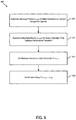
- FIG. 8 is a block diagram illustrating a method 800 of generating a variable clock period for a clock signal of a device at least during a cryptographic operation to defend against a cryptographic attack according to an example embodiment.
- FIG. 8 begins with the initiation ( 805 ) of a cryptographic operation. It is not required that an embodiment of the clock period randomizer described herein initiate the cryptographic operation; a device or unit other than the clock period randomizer may initiate the cryptographic operation. If the cryptographic operation is implemented in software, the software may trigger (e.g. cause) the clock period randomizer to commence a variable clock period that varies randomly to produce an output variable clock driving a device at a random clock rate at least during the cryptographic operation.
- initiation of the hardware for cryptographic operation may trigger (e.g. cause) the clock period randomizer to commence a variable clock period that varies randomly to produce an output variable clock driving a device at a random clock rate at least during the cryptographic operation.
- the clock period randomizer may be supplemented with logic to trigger (e.g. cause) the clock period randomizer to commence a variable clock period that varies randomly to produce an output variable clock driving a device at a random clock rate at least during the cryptographic operation.
- the clock period randomizer commences operation.
- a fixed delay generator generates ( 810 ) a fixed delay.
- the fixed delay generator may comprise a RC circuit, such as the portion of clock period randomizer 450 that includes resistors 415 a - 415 d , inverters 420 a - 420 d , and capacitors 425 a - 425 d .
- the fixed delay generator may comprise t FIXED generator 710 .
- t FIXED may be a temporal component in the time between pulses of VREF of FIG. 11 .
- t FIXED may be a temporal component in the time between digital signals from the digital voltage control input in embodiments of FIG. 11 wherein the voltage regulator 1150 includes the DAC functionality.
- variable delay generator generates ( 820 ) a variable delay.
- the variable delay generator may include inverters 430 a - 430 d , resistors 445 a - 445 d , and variable capacitors 440 a - 440 d and may receive a trim code from the trim code generator 500 .
- the variable delay generator may include tau ( ⁇ ) delay generators 720 and muxes 730 0 - 730 n and may receive a signal from controller 790 .
- the variable delay generator may include switches 1030 a - 1030 n and capacitors 1040 a - 1040 n and may receive from the controller 1090 a trim code generated by the trim code generator 500 .
- variable delay t VAR may be a randomly or pseudorandomly varying temporal component in the time between pulses of VREF of FIG. 11 . In at least one other embodiment, t VAR may be a randomly or pseudorandomly varying temporal component in the time between digital signals from the digital voltage control input in embodiments of FIG. 11 wherein the voltage regulator 1150 includes the DAC functionality.
- a random number generator generates ( 830 ) a random number or a pseudorandom number.
- the random number generator may be the random number generator 330 or 530 .
- an amount of the variable delay is controlled ( 840 ) based on the random number or the pseudorandom number.
- the amount of the variable delay may be controlled, based on the random number or the pseudorandom number, by the trim code generator 500 and the controller 490 , 790 , or 1090 .
- the amount of the variable delay may be controlled, based on the random number or the pseudorandom number, by the controller 1190 .
- the amount of the variable delay may be controlled, based on the random number or the pseudorandom number, by the voltage regulator 1150 which receives a digital signal, wherein the voltage regulator 1150 includes the DAC functionality.
- a variable period of a clock signal is controlled ( 850 ) based on the fixed delay and the variable delay.
- the variable period of the clock signal may be controlled, based on the fixed delay and the variable delay, by the trim code generator 500 and the controller 490 , 790 , or 1090 .
- the variable period of the clock signal may be controlled, based on the fixed delay and the variable delay, by the controller 1190 .
- the variable period of the clock signal may be controlled, based on the fixed delay and the variable delay, by the voltage regulator 1150 which receives a digital signal, wherein the voltage regulator 1150 includes the DAC functionality.
- the device is driven ( 860 ) at the variable clock period at least during cryptographic operation.
- the device may be driven by the output variable clock 365 , 465 , or 1165 .
- FIG. 9 is a block diagram illustrating a method 900 of randomizing a clock period for a clock of an associated device at least during a cryptographic operation to defend against a cryptographic attack according to an example embodiment.
- a set of trim codes is determined ( 910 ), the set including at least a first trim code and a second trim code.
- the set of trim codes may be generated or determined by the trim code generator 500 .
- the set of trim codes may be determined by a person having ordinary skill in the art based on the number(s) of bits each trim code in the set of trim code may comprise. Factors relevant to the number(s) of bits each trim code in the set of trim code may include the number of elements which the trim codes are used to control and the number of desired or permissible states of the elements which the trim codes are used to control.
- physical electronic hardware generates ( 920 ) a random number or a pseudorandom number.
- the random number or the pseudorandom number may be generated by the random number generator 330 or 530 .
- the first trim code is selected ( 930 ) from the set of trim codes based on the random number or the pseudorandom number.
- the first trim code from the set of trim codes may be selected, based on the random number or the pseudorandom number, by the trim code generator 500 , including m-bit pseudorandom binary sequence generator 515 , logic gate 510 , shift register comprising flip flops 520 a - 520 m , modular arithmetic calculator 512 , a register bank comprising registers 540 a - 540 p , and mux 550 .
- the second trim code is selected ( 940 ) from the set of trim codes based on the random number or the pseudorandom number.
- the second trim code from the set of trim codes may be selected, based on the random number or the pseudorandom number, by the trim code generator 500 , including m-bit pseudorandom binary sequence generator 515 , logic gate 510 , shift register comprising flip flops 520 a - 520 m , modular arithmetic calculator 512 , a register bank comprising registers 540 a - 540 p , and mux 550 .
- the first trim code is provided ( 950 ) to a variable delay generator, the variable delay generator including elements that operate based on any trim code from the set of trim codes.
- the set of trim codes may include only the trim codes for permissible states; in at least one embodiment, not all permutations of a bit vector of a certain length may be trim codes for permissible states because some permutations, when applied, may result in configurations (e.g. hardware configurations or switch configurations) which are not useful, desired, effective, and/or legal.
- the variable delay generator may include inverters 430 a - 430 d , resistors 445 a - 445 d , and variable capacitors 440 a - 440 d and may receive the first trim code and the second trim code from the trim code generator 500 .
- the variable delay generator may include tau ( ⁇ ) delay generators 720 and muxes 730 0 - 730 n and may receive a signal from controller 790 , the signal comprising the first trim code and the second trim code.
- the variable delay generator may include switches 1030 a - 1030 n and capacitors 1040 a - 1040 n and may receive from the controller 1090 the first trim code and the second trim code.
- variable delay t VAR may be a randomly or pseudorandomly varying temporal component in the time between pulses of VREF of FIG. 11
- the random or pseudorandom variance may be a function of the first trim code or and the second trim code, the function determined or calculated by logic comprising integrated circuitry or by the controller 1190 .
- t VAR may be a randomly or pseudorandomly varying temporal component in the time between digital signals from the digital voltage control input in embodiments of FIG. 11 wherein the voltage regulator 1150 includes the DAC functionality, and the digital signals are a function of the first trim code or the second trim code or comprise the first trim code or the second trim code.
- the second trim code is provided ( 960 ) to the variable delay generator, wherein when the first trim code is provided to the variable delay generator, a clock period of the associated device is a first amount of time, wherein when the second trim code is provided to the variable delay generator, a clock period of the associated device is a second amount of time, and wherein the first amount of time is at least 1% greater than the second amount of time.
- a “cryptographic operation” comprises an operation included in a cryptographic algorithm.
- a “cryptographic operation” further comprises an operation on a private key.
- Cryptographic algorithms include, but are not limited to, the algorithms provided in Federal Information Processing Standards Publication 202 (SHA-3 standard) and Federal Information Processing Standards Publication 197 (AES standard).
Landscapes
- Engineering & Computer Science (AREA)
- Computer Security & Cryptography (AREA)
- Computer Networks & Wireless Communication (AREA)
- Signal Processing (AREA)
- Physics & Mathematics (AREA)
- Theoretical Computer Science (AREA)
- General Physics & Mathematics (AREA)
- Mathematical Optimization (AREA)
- Mathematical Analysis (AREA)
- Pure & Applied Mathematics (AREA)
- General Engineering & Computer Science (AREA)
- Computational Mathematics (AREA)
- Pulse Circuits (AREA)
- Manipulation Of Pulses (AREA)
- Semiconductor Integrated Circuits (AREA)
- Test And Diagnosis Of Digital Computers (AREA)
- Debugging And Monitoring (AREA)
- Stabilization Of Oscillater, Synchronisation, Frequency Synthesizers (AREA)
Abstract
Description
Claims (29)
Priority Applications (10)
| Application Number | Priority Date | Filing Date | Title |
|---|---|---|---|
| US15/436,489 US10958414B2 (en) | 2016-02-23 | 2017-02-17 | Clock period randomization for defense against cryptographic attacks |
| EP17708948.9A EP3420667B1 (en) | 2016-02-23 | 2017-02-22 | Clock period randomization for defense against cryptographic attacks |
| DE212017000013.9U DE212017000013U1 (en) | 2016-02-23 | 2017-02-22 | Clock period randomization device for defense against cryptographic attacks |
| DE112017000048.3T DE112017000048B4 (en) | 2016-02-23 | 2017-02-22 | Clock period randomization to defend against cryptographic attacks |
| PCT/US2017/018813 WO2017147116A1 (en) | 2016-02-23 | 2017-02-22 | Clock period randomization for defense against cryptographic attacks |
| CN201780000669.2A CN107735981B (en) | 2016-02-23 | 2017-02-22 | Clock period randomization for defense against cryptographic attacks |
| GB1717083.8A GB2555725B (en) | 2016-02-23 | 2017-02-22 | Clock period randomization for defense against cryptographic attacks |
| JP2018525379A JP6621533B2 (en) | 2016-02-23 | 2017-02-22 | Clock cycle randomization for protection against cryptographic attacks |
| JP2019208908A JP7094932B2 (en) | 2016-02-23 | 2019-11-19 | Randomized clock period to protect against cryptographic attacks |
| US17/176,554 US11750361B2 (en) | 2016-02-23 | 2021-02-16 | Clock period randomization for defense against cryptographic attacks |
Applications Claiming Priority (2)
| Application Number | Priority Date | Filing Date | Title |
|---|---|---|---|
| US201662298842P | 2016-02-23 | 2016-02-23 | |
| US15/436,489 US10958414B2 (en) | 2016-02-23 | 2017-02-17 | Clock period randomization for defense against cryptographic attacks |
Related Child Applications (1)
| Application Number | Title | Priority Date | Filing Date |
|---|---|---|---|
| US17/176,554 Continuation US11750361B2 (en) | 2016-02-23 | 2021-02-16 | Clock period randomization for defense against cryptographic attacks |
Publications (2)
| Publication Number | Publication Date |
|---|---|
| US20170244546A1 US20170244546A1 (en) | 2017-08-24 |
| US10958414B2 true US10958414B2 (en) | 2021-03-23 |
Family
ID=59630310
Family Applications (2)
| Application Number | Title | Priority Date | Filing Date |
|---|---|---|---|
| US15/436,489 Active 2038-11-16 US10958414B2 (en) | 2016-02-23 | 2017-02-17 | Clock period randomization for defense against cryptographic attacks |
| US17/176,554 Active 2037-11-12 US11750361B2 (en) | 2016-02-23 | 2021-02-16 | Clock period randomization for defense against cryptographic attacks |
Family Applications After (1)
| Application Number | Title | Priority Date | Filing Date |
|---|---|---|---|
| US17/176,554 Active 2037-11-12 US11750361B2 (en) | 2016-02-23 | 2021-02-16 | Clock period randomization for defense against cryptographic attacks |
Country Status (7)
| Country | Link |
|---|---|
| US (2) | US10958414B2 (en) |
| EP (1) | EP3420667B1 (en) |
| JP (2) | JP6621533B2 (en) |
| CN (1) | CN107735981B (en) |
| DE (2) | DE212017000013U1 (en) |
| GB (1) | GB2555725B (en) |
| WO (1) | WO2017147116A1 (en) |
Cited By (7)
| Publication number | Priority date | Publication date | Assignee | Title |
|---|---|---|---|---|
| US20210194667A1 (en) * | 2016-02-23 | 2021-06-24 | Google Llc | Clock Period Randomization for Defense Against Cryptographic Attacks |
| US11283349B2 (en) * | 2020-04-23 | 2022-03-22 | Nvidia Corp. | Techniques to improve current regulator capability to protect the secured circuit from power side channel attack |
| US11507704B2 (en) | 2020-04-23 | 2022-11-22 | Nvidia Corp. | Current flattening circuit for protection against power side channel attacks |
| US11651194B2 (en) | 2019-11-27 | 2023-05-16 | Nvidia Corp. | Layout parasitics and device parameter prediction using graph neural networks |
| US12499956B2 (en) | 2022-12-06 | 2025-12-16 | Micron Technology, Inc. | Glitch detection |
| US12499226B2 (en) | 2023-02-27 | 2025-12-16 | Nxp B.V. | Circuit and method for protecting an application against a side channel attack |
| US12547778B2 (en) | 2021-12-22 | 2026-02-10 | Samsung Electronics Co., Ltd. | Malicious attack protection circuit, system-on-chip including the same, and operating method thereof |
Families Citing this family (29)
| Publication number | Priority date | Publication date | Assignee | Title |
|---|---|---|---|---|
| US10951391B2 (en) * | 2015-09-06 | 2021-03-16 | Bar-Ilan University | Randomized logic against side channel attacks |
| CN105894079B (en) * | 2016-04-22 | 2019-03-15 | 上海东软载波微电子有限公司 | Clock scrambling circuit |
| US10609068B2 (en) * | 2017-10-18 | 2020-03-31 | International Business Machines Corporation | Identification of attack flows in a multi-tier network topology |
| US10305479B1 (en) * | 2018-06-12 | 2019-05-28 | Nxp B.V. | Fault attack protection against synchronized fault injections |
| US10263767B1 (en) | 2018-07-03 | 2019-04-16 | Rajant Corporation | System and method for power analysis resistant clock |
| US10878133B2 (en) * | 2018-11-18 | 2020-12-29 | Nuvoton Technology Corporation | Mitigation of side-channel attacks using small-overhead random pre-charging |
| CN109861818A (en) * | 2019-03-06 | 2019-06-07 | 京东方科技集团股份有限公司 | Encryption and decryption circuit, encryption and decryption device, and encryption and decryption method |
| CN110298200B (en) * | 2019-07-05 | 2023-05-02 | 电子科技大学 | ASIC chip hardware back door detection method based on temperature statistics feature analysis |
| CN110726483B (en) * | 2019-09-30 | 2021-10-08 | 安徽问天量子科技股份有限公司 | Device and method for resisting avalanche transition region attack |
| FR3102268B1 (en) * | 2019-10-18 | 2023-03-10 | St Microelectronics Rousset | Circuit-on-chip authentication method and associated system-on-chip |
| CN114586034B (en) | 2019-11-19 | 2025-10-17 | 谷歌有限责任公司 | Voltage change detection under clock fluctuation |
| KR102348912B1 (en) * | 2019-12-06 | 2022-01-11 | 주식회사 이와이엘 | Random number generator for defense against side-channel attacks and Method for operating the same |
| KR102374329B1 (en) * | 2020-07-28 | 2022-03-14 | 경북대학교 산학협력단 | Apparatus and method for preventing power analysis attack using voltage change |
| US11741227B2 (en) | 2021-06-22 | 2023-08-29 | Intel Corporation | Platform security mechanism |
| US11762993B2 (en) * | 2021-04-12 | 2023-09-19 | Nxp B.V. | Securing cryptographic operations from side channel attacks using a chaotic oscillator |
| CN113111395B (en) * | 2021-04-20 | 2025-03-28 | 青芯半导体科技(上海)有限公司 | Scrambled clock generation circuit |
| GB202107381D0 (en) * | 2021-05-24 | 2021-07-07 | Nordic Semiconductor Asa | Security in integrated circuits |
| US12174955B2 (en) * | 2021-06-22 | 2024-12-24 | Intel Corporation | Integrated circuit side-channel mitigation mechanism |
| TWI773430B (en) * | 2021-07-09 | 2022-08-01 | 新唐科技股份有限公司 | Security activating system and method thereof |
| JP7710936B2 (en) * | 2021-09-06 | 2025-07-22 | キヤノン株式会社 | Information processing device, information processing method, and program |
| JP7653904B2 (en) * | 2021-11-29 | 2025-03-31 | ルネサスエレクトロニクス株式会社 | Semiconductor device and clock control method |
| CN114048470B (en) * | 2022-01-13 | 2022-06-24 | 浙江大学 | Method and device for defending hardware attack based on TDC module and electronic equipment |
| TWI818503B (en) * | 2022-04-11 | 2023-10-11 | 新唐科技股份有限公司 | Encryption device and encryption method |
| US20240235806A9 (en) * | 2022-10-25 | 2024-07-11 | Microsoft Technology Licensing, Llc | Detecting and mitigating side channel attacks with razor-flops |
| GB202216890D0 (en) * | 2022-11-11 | 2022-12-28 | Nordic Semiconductor Asa | Mitigating side channel attacks |
| WO2025239895A1 (en) * | 2024-05-16 | 2025-11-20 | Google Llc | Digital clock jitter circuit for security countermeasures |
| US20250355672A1 (en) * | 2024-05-20 | 2025-11-20 | Stmicroelectronics International N.V. | Hardware randomized boot clock |
| CN119247285B (en) * | 2024-12-04 | 2025-03-07 | 成都天成电科科技有限公司 | Encryption method, transmitting end and receiving end of modulation signal |
| CN119336125B (en) * | 2024-12-23 | 2025-07-11 | 深圳市纽创信安科技开发有限公司 | Random clock generating device and clock signal output method |
Citations (27)
| Publication number | Priority date | Publication date | Assignee | Title |
|---|---|---|---|---|
| US4932053A (en) | 1988-11-10 | 1990-06-05 | Sgs-Thomson Microelectronics, S.A. | Safety device against the unauthorized detection of protected data |
| US5164677A (en) | 1990-01-16 | 1992-11-17 | Digital Equipment Corporation | Method and apparatus for synchronizing signals |
| US5404402A (en) | 1993-12-21 | 1995-04-04 | Gi Corporation | Clock frequency modulation for secure microprocessors |
| CN1190830A (en) | 1997-01-16 | 1998-08-19 | 日本电气株式会社 | Pseudo-random number generation circuit and its application in data communication system |
| JP2001126480A (en) | 1999-10-29 | 2001-05-11 | Fujitsu Ltd | Semiconductor integrated circuit, control method of semiconductor integrated circuit, and variable delay circuit |
| JP2003178589A (en) | 2001-12-10 | 2003-06-27 | Toshiba Corp | Nonvolatile semiconductor memory device |
| US20030210101A1 (en) * | 2002-02-26 | 2003-11-13 | Mccorquodale Michael S. | MEMS-based, computer systems, clock generation and oscillator circuits and LC-tank apparatus for use therein |
| JP2003337750A (en) | 2002-05-22 | 2003-11-28 | Hitachi Ltd | Semiconductor device with internal analysis prevention function |
| US20030231122A1 (en) | 2002-06-14 | 2003-12-18 | International Business Machines Corporation | Multi-byte Lempel-Ziv 1(LZ1) decompression |
| US20050231296A1 (en) | 2004-02-12 | 2005-10-20 | Zarlink Semiconductor Ab | Directly modulated CMOS VCO |
| US6987405B1 (en) | 2002-10-18 | 2006-01-17 | Mips Technologies, Inc. | Apparatus and method for generating multi-phase signals with digitally controlled trim capacitors |
| JP2007248380A (en) | 2006-03-17 | 2007-09-27 | Fujitsu Ltd | Delay time evaluation method and circuit, and semiconductor device |
| JP2008113130A (en) | 2006-10-30 | 2008-05-15 | Sharp Corp | Encryption device |
| US20090163166A1 (en) * | 2007-12-21 | 2009-06-25 | Realtek Semiconductor Corp. | Phase lock loop with phase interpolation by reference clock and method for the same |
| US20100007398A1 (en) * | 2008-07-11 | 2010-01-14 | Integrated Device Technology, Inc. | Linear monotonic delay chain circuit |
| US20110074509A1 (en) * | 2008-03-31 | 2011-03-31 | Anil Samavedam | Non-linear capacitance compensation |
| US20110285420A1 (en) | 2010-05-24 | 2011-11-24 | Alexander Roger Deas | Logic system with resistance to side-channel attack by exhibiting a closed clock-data eye diagram |
| US20110296202A1 (en) * | 2010-05-25 | 2011-12-01 | Via Technologies, Inc. | Switch key instruction in a microprocessor that fetches and decrypts encrypted instructions |
| US8266194B2 (en) * | 2007-12-12 | 2012-09-11 | Nds Limited | Linear feedback shift registers with XOR logic gates including a bit generator to control movement along stages |
| US20130222067A1 (en) * | 2012-02-28 | 2013-08-29 | Kawasaki Microelectronics Inc. | Phase-locked loop |
| CN103378828A (en) | 2012-04-25 | 2013-10-30 | 飞思卡尔半导体公司 | Fine tuning circuit for clock source |
| US20140225110A1 (en) | 2013-02-12 | 2014-08-14 | Texas Instruments Incorporated | Default Trim Code Technique |
| GB2513987A (en) | 2013-03-15 | 2014-11-12 | Intel Corp | Parallel apparatus for high-speed, highly compressed LZ77 tokenization and huffman encoding for deflate compression |
| US9046552B2 (en) | 2013-03-15 | 2015-06-02 | Intel Corporation | On-die trim-able passive components for high volume manufacturing |
| WO2015145487A1 (en) | 2014-03-28 | 2015-10-01 | 三菱電機株式会社 | Clock phase control circuit |
| WO2016178826A1 (en) | 2015-05-01 | 2016-11-10 | Google Inc. | Asic block for high bandwidth lz77 decompression |
| WO2017147116A1 (en) | 2016-02-23 | 2017-08-31 | Google Inc. | Clock period randomization for defense against cryptographic attacks |
Family Cites Families (9)
| Publication number | Priority date | Publication date | Assignee | Title |
|---|---|---|---|---|
| CN101739061B (en) * | 2009-12-04 | 2015-06-03 | 威盛电子股份有限公司 | Clock generator and universal serial bus module |
| CN102254110A (en) * | 2010-05-20 | 2011-11-23 | 中国人民解放军国防科学技术大学 | Control circuit for randomization of overturning moment of register |
| US20110299678A1 (en) * | 2010-06-07 | 2011-12-08 | Alexander Roger Deas | Secure means for generating a specific key from unrelated parameters |
| KR20120095699A (en) * | 2011-02-21 | 2012-08-29 | 에스케이하이닉스 주식회사 | Phase interpolator |
| US8692599B2 (en) | 2012-08-22 | 2014-04-08 | Silicon Laboratories Inc. | Interpolative divider linearity enhancement techniques |
| US8971447B1 (en) * | 2013-10-17 | 2015-03-03 | Fujitsu Limited | Variable delay of data signals |
| JP6323065B2 (en) * | 2014-02-26 | 2018-05-16 | セイコーエプソン株式会社 | Microcomputer and electronic equipment |
| US9252792B2 (en) * | 2014-05-12 | 2016-02-02 | Texas Instruments Incorporated | Tunable frequency-to-voltage controlled oscillation |
| CN105894079B (en) | 2016-04-22 | 2019-03-15 | 上海东软载波微电子有限公司 | Clock scrambling circuit |
-
2017
- 2017-02-17 US US15/436,489 patent/US10958414B2/en active Active
- 2017-02-22 JP JP2018525379A patent/JP6621533B2/en active Active
- 2017-02-22 EP EP17708948.9A patent/EP3420667B1/en active Active
- 2017-02-22 DE DE212017000013.9U patent/DE212017000013U1/en active Active
- 2017-02-22 WO PCT/US2017/018813 patent/WO2017147116A1/en not_active Ceased
- 2017-02-22 GB GB1717083.8A patent/GB2555725B/en active Active
- 2017-02-22 CN CN201780000669.2A patent/CN107735981B/en active Active
- 2017-02-22 DE DE112017000048.3T patent/DE112017000048B4/en active Active
-
2019
- 2019-11-19 JP JP2019208908A patent/JP7094932B2/en active Active
-
2021
- 2021-02-16 US US17/176,554 patent/US11750361B2/en active Active
Patent Citations (33)
| Publication number | Priority date | Publication date | Assignee | Title |
|---|---|---|---|---|
| US4932053A (en) | 1988-11-10 | 1990-06-05 | Sgs-Thomson Microelectronics, S.A. | Safety device against the unauthorized detection of protected data |
| US5164677A (en) | 1990-01-16 | 1992-11-17 | Digital Equipment Corporation | Method and apparatus for synchronizing signals |
| US5404402A (en) | 1993-12-21 | 1995-04-04 | Gi Corporation | Clock frequency modulation for secure microprocessors |
| JPH07239837A (en) | 1993-12-21 | 1995-09-12 | General Instr Corp Of Delaware | Clock frequency modulation for a secret microprocessor. |
| CN1190830A (en) | 1997-01-16 | 1998-08-19 | 日本电气株式会社 | Pseudo-random number generation circuit and its application in data communication system |
| JP2001126480A (en) | 1999-10-29 | 2001-05-11 | Fujitsu Ltd | Semiconductor integrated circuit, control method of semiconductor integrated circuit, and variable delay circuit |
| US20020093872A1 (en) | 1999-10-29 | 2002-07-18 | Fujitsu Limited | Semiconductor integrated circuit, method of controlling the same, and variable delay circuit |
| US6930954B2 (en) | 2001-12-10 | 2005-08-16 | Kabushiki Kaisha Toshiba | Non-volatile semiconductor memory device |
| JP2003178589A (en) | 2001-12-10 | 2003-06-27 | Toshiba Corp | Nonvolatile semiconductor memory device |
| US20030210101A1 (en) * | 2002-02-26 | 2003-11-13 | Mccorquodale Michael S. | MEMS-based, computer systems, clock generation and oscillator circuits and LC-tank apparatus for use therein |
| JP2003337750A (en) | 2002-05-22 | 2003-11-28 | Hitachi Ltd | Semiconductor device with internal analysis prevention function |
| US20030231122A1 (en) | 2002-06-14 | 2003-12-18 | International Business Machines Corporation | Multi-byte Lempel-Ziv 1(LZ1) decompression |
| US6987405B1 (en) | 2002-10-18 | 2006-01-17 | Mips Technologies, Inc. | Apparatus and method for generating multi-phase signals with digitally controlled trim capacitors |
| US20050231296A1 (en) | 2004-02-12 | 2005-10-20 | Zarlink Semiconductor Ab | Directly modulated CMOS VCO |
| JP2007248380A (en) | 2006-03-17 | 2007-09-27 | Fujitsu Ltd | Delay time evaluation method and circuit, and semiconductor device |
| JP2008113130A (en) | 2006-10-30 | 2008-05-15 | Sharp Corp | Encryption device |
| CN101542969A (en) | 2006-10-30 | 2009-09-23 | 夏普株式会社 | Encrypting apparatus |
| US8266194B2 (en) * | 2007-12-12 | 2012-09-11 | Nds Limited | Linear feedback shift registers with XOR logic gates including a bit generator to control movement along stages |
| US20090163166A1 (en) * | 2007-12-21 | 2009-06-25 | Realtek Semiconductor Corp. | Phase lock loop with phase interpolation by reference clock and method for the same |
| US20110074509A1 (en) * | 2008-03-31 | 2011-03-31 | Anil Samavedam | Non-linear capacitance compensation |
| US20100007398A1 (en) * | 2008-07-11 | 2010-01-14 | Integrated Device Technology, Inc. | Linear monotonic delay chain circuit |
| US20110285420A1 (en) | 2010-05-24 | 2011-11-24 | Alexander Roger Deas | Logic system with resistance to side-channel attack by exhibiting a closed clock-data eye diagram |
| US20110296202A1 (en) * | 2010-05-25 | 2011-12-01 | Via Technologies, Inc. | Switch key instruction in a microprocessor that fetches and decrypts encrypted instructions |
| US20130222067A1 (en) * | 2012-02-28 | 2013-08-29 | Kawasaki Microelectronics Inc. | Phase-locked loop |
| US20130285729A1 (en) * | 2012-04-25 | 2013-10-31 | Freescale Semiconductor, Inc | Trimming circuit for clock source |
| CN103378828A (en) | 2012-04-25 | 2013-10-30 | 飞思卡尔半导体公司 | Fine tuning circuit for clock source |
| US20140225110A1 (en) | 2013-02-12 | 2014-08-14 | Texas Instruments Incorporated | Default Trim Code Technique |
| GB2513987A (en) | 2013-03-15 | 2014-11-12 | Intel Corp | Parallel apparatus for high-speed, highly compressed LZ77 tokenization and huffman encoding for deflate compression |
| US9046552B2 (en) | 2013-03-15 | 2015-06-02 | Intel Corporation | On-die trim-able passive components for high volume manufacturing |
| WO2015145487A1 (en) | 2014-03-28 | 2015-10-01 | 三菱電機株式会社 | Clock phase control circuit |
| WO2016178826A1 (en) | 2015-05-01 | 2016-11-10 | Google Inc. | Asic block for high bandwidth lz77 decompression |
| WO2017147116A1 (en) | 2016-02-23 | 2017-08-31 | Google Inc. | Clock period randomization for defense against cryptographic attacks |
| CN107735981A (en) | 2016-02-23 | 2018-02-23 | 谷歌有限责任公司 | Clock cycle randomization for defense against cryptographic attacks |
Non-Patent Citations (21)
| Title |
|---|
| "Application Note // Hardware GZIP Decompression", Internet article; As cited in search report for PCT application PCT/US2016/0238630 dated Nov. 10, 2016, 2003, p. 7. |
| "Foreign Office Action", Chinese Application No. 201780000669.2, dated Apr. 9, 2020, 42 pages. |
| "Foreign Office Action", CN Application 201780000669.2, dated Dec. 8, 2020, 9 pages. |
| "Foreign Office Action", Japanese Application No. 2018525379, dated Jul. 9, 2019, 6 pages. |
| "Foreign Office Action", Japanese Application No. 2018525379, dated Nov. 6, 2018, 6 pages. |
| "International Preliminary Report on Patentability", PCT Application No. PCT/US2017/018813, dated Aug. 28, 2018, 10 pages. |
| "Written Opinion", PCT Application No. PCT/US2016/028630, dated Nov. 10, 2016, 6 pages. |
| "Written Opinion", PCT Application No. PCT/US2017/018813, dated Aug. 31, 2017, 9 pages. |
| Aoyama, Morishige et al. 3Gbps, 5000ppm Spread Spectrum SerDes PHY with frequency tracking Phase Interpolator for Serial ATA, 2003 Symposium on VLSI Circuits Digest of Technical Papers, 107-110. |
| Asai, et al., "A Countermeasure Against Side Channel Attack on Cryptographic LSI Using Clock Variation Mechanism", 2013, 11 pages. |
| Bar-El, Nagai, et al. "The sorcerer's apprentice guide to fault attacks." Proceedings of the IEEE 94, No. 2 (2006): 370-382. |
| Bayrak et al., (an EDA-Friendly Protection Scheme against Side-Channel Attacks, EDAA 2013, 6 pages) (Year: 2013). * |
| Bayrak, et al., "An EDA-Friendly Protection Scheme Against Side-Channel Attacks", 2013 Design, Automation & Test in Europe Conference & Exhibition, US, IEEE, Mar. 18, 2013, Mar. 18, 2013, 8 pages. |
| Bialek et al. (Implementation of a digital trim scheme for SAR ADCs, Adv. Radio Sci., 11, 227-230, 2013) (Year: 2013). * |
| Horinouchi, et al., "Variation of Fault Attack Possibility with Jitter in Synchronization Signal Leaked Through Side-Channel of AES Circuit", SCIS2016[USB], Japan, Jan. 19, 2016, 2F3-3, pp. 1-7, Jan. 19, 2016, 12 pages. |
| Kocher, Paul C. "Timing attacks on implementations of Diffie-Hellman, RSA, DSS, and other systems." In Annual International Cryptology Conference, pp. 104-113. Springer Berlin Heidelberg, 1996. |
| Saeki, Takanori, et al. "A 2.5-ns clock access, 250-MHz, 256-Mb SDRAM with synchronous mirror delay." IEEE Journal of Solid-State Circuits 31, No. 11 (1996): 1656-1668. |
| Sidiropoulos, Stefanos, et al. "A semidigital dual delay-locked loop." IEEE Journal of Solid-State Circuits 32, No. 11 (1997): 1683-1692. |
| Toshiya Asai, et al. A Countermeasure Against Side Channel Attack Cryptographic LSI using Clock Variation Mechanism. IEEJ Transaction on Electronics, Information and Systems, Dec. 1, 2013, vol. 133 No. 12, pp. 2134-2142 (Year: 2013). * |
| Zafar, et al., "A Novel Countermeasure Enhancing Side Channel Immunity in FPGAs", 2008 International Conference on Advances in Electronics and Micro-electronics, US, IEEE, Sep. 29, 2008, pp. 132-137, Sep. 29, 2008, 8 pages. |
| Zafar, et al., "A Novel Countermeasure Enhancing Side Channel Immunity in FPGAs", cited in search report of PCT pplication PCT/US2017/018813 dated May 5, 2017, dated Oct. 10, 2008, 3 pages. |
Cited By (11)
| Publication number | Priority date | Publication date | Assignee | Title |
|---|---|---|---|---|
| US20210194667A1 (en) * | 2016-02-23 | 2021-06-24 | Google Llc | Clock Period Randomization for Defense Against Cryptographic Attacks |
| US11750361B2 (en) * | 2016-02-23 | 2023-09-05 | Google Llc | Clock period randomization for defense against cryptographic attacks |
| US11651194B2 (en) | 2019-11-27 | 2023-05-16 | Nvidia Corp. | Layout parasitics and device parameter prediction using graph neural networks |
| US12217151B2 (en) | 2019-11-27 | 2025-02-04 | Nvidia Corp. | Layout parasitics and device parameter prediction using graph neural networks |
| US11283349B2 (en) * | 2020-04-23 | 2022-03-22 | Nvidia Corp. | Techniques to improve current regulator capability to protect the secured circuit from power side channel attack |
| US11507704B2 (en) | 2020-04-23 | 2022-11-22 | Nvidia Corp. | Current flattening circuit for protection against power side channel attacks |
| US11594962B2 (en) | 2020-04-23 | 2023-02-28 | Nvidia Corp. | Techniques to improve current regulator capability to protect the secured circuit from power side channel attack |
| US11687679B2 (en) | 2020-04-23 | 2023-06-27 | Nvidia Corp. | Current flattening circuit for protection against power side channel attacks |
| US12547778B2 (en) | 2021-12-22 | 2026-02-10 | Samsung Electronics Co., Ltd. | Malicious attack protection circuit, system-on-chip including the same, and operating method thereof |
| US12499956B2 (en) | 2022-12-06 | 2025-12-16 | Micron Technology, Inc. | Glitch detection |
| US12499226B2 (en) | 2023-02-27 | 2025-12-16 | Nxp B.V. | Circuit and method for protecting an application against a side channel attack |
Also Published As
| Publication number | Publication date |
|---|---|
| US11750361B2 (en) | 2023-09-05 |
| CN107735981B (en) | 2021-06-25 |
| JP6621533B2 (en) | 2019-12-18 |
| US20170244546A1 (en) | 2017-08-24 |
| JP2018535606A (en) | 2018-11-29 |
| CN107735981A (en) | 2018-02-23 |
| DE212017000013U1 (en) | 2018-01-29 |
| DE112017000048T5 (en) | 2018-08-16 |
| JP2020058034A (en) | 2020-04-09 |
| EP3420667B1 (en) | 2020-09-30 |
| EP3420667A1 (en) | 2019-01-02 |
| JP7094932B2 (en) | 2022-07-04 |
| GB2555725A (en) | 2018-05-09 |
| US20210194667A1 (en) | 2021-06-24 |
| DE112017000048B4 (en) | 2024-02-15 |
| WO2017147116A1 (en) | 2017-08-31 |
| GB2555725B (en) | 2021-11-10 |
| GB201717083D0 (en) | 2017-11-29 |
Similar Documents
| Publication | Publication Date | Title |
|---|---|---|
| US11750361B2 (en) | Clock period randomization for defense against cryptographic attacks | |
| CN108073383B (en) | Enhanced random number generator | |
| JP4893895B2 (en) | Multi-bit sampling of oscillator jitter for random number generation | |
| KR20100127789A (en) | Digital random number generator based on digitally controlled oscillator | |
| US10263767B1 (en) | System and method for power analysis resistant clock | |
| KR101946509B1 (en) | System and method for protection from side-channel attacks by varying clock delays | |
| US9830130B2 (en) | Random number generator | |
| Lampert et al. | Robust, low-cost, auditable random number generation for embedded system security | |
| US20230176820A1 (en) | Random number generator and random number generation method | |
| JP7122142B2 (en) | Computing system with power fluctuation attack countermeasures | |
| CN116368463A (en) | Random number generator and random number generation method | |
| EP1562291A1 (en) | Apparatus for providing a random bit stream | |
| US9525457B1 (en) | Spread spectrum clock generation using a tapped delay line and entropy injection | |
| Luo et al. | Faulty clock detection for crypto circuits against differential fault analysis attack | |
| Garipcan et al. | Implementation of a digital TRNG using jitter based multiple entropy source on FPGA | |
| Soorat et al. | Hardware Random number Generator for cryptography | |
| EP3767849A1 (en) | A hardware component and a method for implementing a camouflage of current traces generated by a digital system | |
| Lee et al. | Metastability-based feedback method for enhancing fpga-based trng | |
| CN119645348A (en) | A pseudo-random sequence generating circuit and address sampling circuit | |
| EP3203460A1 (en) | Secure data storage | |
| US20150019603A1 (en) | Method for checking an output of a random number generator | |
| Jiménez et al. | FPGA implementation of hardware countermeasures | |
| Kilinc | True random number generation based on double-scroll chaotic system | |
| Mandrona et al. | Development of a statistically reliable pseudorandom bit sequence | |
| WO2014200326A1 (en) | Device and method for outputting random data |
Legal Events
| Date | Code | Title | Description |
|---|---|---|---|
| AS | Assignment |
Owner name: GOOGLE INC., CALIFORNIA Free format text: ASSIGNMENT OF ASSIGNORS INTEREST;ASSIGNOR:STARK, DONALD;REEL/FRAME:041322/0987 Effective date: 20170217 |
|
| AS | Assignment |
Owner name: GOOGLE LLC, CALIFORNIA Free format text: CHANGE OF NAME;ASSIGNOR:GOOGLE INC.;REEL/FRAME:044129/0001 Effective date: 20170929 |
|
| STPP | Information on status: patent application and granting procedure in general |
Free format text: RESPONSE TO NON-FINAL OFFICE ACTION ENTERED AND FORWARDED TO EXAMINER |
|
| STPP | Information on status: patent application and granting procedure in general |
Free format text: FINAL REJECTION MAILED |
|
| STPP | Information on status: patent application and granting procedure in general |
Free format text: RESPONSE AFTER FINAL ACTION FORWARDED TO EXAMINER |
|
| STPP | Information on status: patent application and granting procedure in general |
Free format text: ADVISORY ACTION MAILED |
|
| STCV | Information on status: appeal procedure |
Free format text: NOTICE OF APPEAL FILED |
|
| STCV | Information on status: appeal procedure |
Free format text: APPEAL BRIEF (OR SUPPLEMENTAL BRIEF) ENTERED AND FORWARDED TO EXAMINER |
|
| STCV | Information on status: appeal procedure |
Free format text: EXAMINER'S ANSWER TO APPEAL BRIEF MAILED |
|
| STCB | Information on status: application discontinuation |
Free format text: ABANDONED -- AFTER EXAMINER'S ANSWER OR BOARD OF APPEALS DECISION |
|
| STCV | Information on status: appeal procedure |
Free format text: ON APPEAL -- AWAITING DECISION BY THE BOARD OF APPEALS |
|
| STCV | Information on status: appeal procedure |
Free format text: BOARD OF APPEALS DECISION RENDERED |
|
| STPP | Information on status: patent application and granting procedure in general |
Free format text: NOTICE OF ALLOWANCE MAILED -- APPLICATION RECEIVED IN OFFICE OF PUBLICATIONS |
|
| STCF | Information on status: patent grant |
Free format text: PATENTED CASE |
|
| MAFP | Maintenance fee payment |
Free format text: PAYMENT OF MAINTENANCE FEE, 4TH YEAR, LARGE ENTITY (ORIGINAL EVENT CODE: M1551); ENTITY STATUS OF PATENT OWNER: LARGE ENTITY Year of fee payment: 4 |