US10886187B2 - Thermal management in integrated circuit using phononic bandgap structure - Google Patents
Thermal management in integrated circuit using phononic bandgap structure Download PDFInfo
- Publication number
- US10886187B2 US10886187B2 US15/792,580 US201715792580A US10886187B2 US 10886187 B2 US10886187 B2 US 10886187B2 US 201715792580 A US201715792580 A US 201715792580A US 10886187 B2 US10886187 B2 US 10886187B2
- Authority
- US
- United States
- Prior art keywords
- die
- encapsulation material
- integrated circuit
- nodes
- phononic
- Prior art date
- Legal status (The legal status is an assumption and is not a legal conclusion. Google has not performed a legal analysis and makes no representation as to the accuracy of the status listed.)
- Active, expires
Links
Images


Classifications
-
- H10W74/481—
-
- H—ELECTRICITY
- H01—ELECTRIC ELEMENTS
- H01L—SEMICONDUCTOR DEVICES NOT COVERED BY CLASS H10
- H01L23/00—Details of semiconductor or other solid state devices
- H01L23/28—Encapsulations, e.g. encapsulating layers, coatings, e.g. for protection
- H01L23/29—Encapsulations, e.g. encapsulating layers, coatings, e.g. for protection characterised by the material, e.g. carbon
- H01L23/298—Semiconductor material, e.g. amorphous silicon
-
- G—PHYSICS
- G10—MUSICAL INSTRUMENTS; ACOUSTICS
- G10K—SOUND-PRODUCING DEVICES; METHODS OR DEVICES FOR PROTECTING AGAINST, OR FOR DAMPING, NOISE OR OTHER ACOUSTIC WAVES IN GENERAL; ACOUSTICS NOT OTHERWISE PROVIDED FOR
- G10K11/00—Methods or devices for transmitting, conducting or directing sound in general; Methods or devices for protecting against, or for damping, noise or other acoustic waves in general
- G10K11/16—Methods or devices for protecting against, or for damping, noise or other acoustic waves in general
- G10K11/162—Selection of materials
-
- H—ELECTRICITY
- H01—ELECTRIC ELEMENTS
- H01L—SEMICONDUCTOR DEVICES NOT COVERED BY CLASS H10
- H01L23/00—Details of semiconductor or other solid state devices
- H01L23/28—Encapsulations, e.g. encapsulating layers, coatings, e.g. for protection
- H01L23/29—Encapsulations, e.g. encapsulating layers, coatings, e.g. for protection characterised by the material, e.g. carbon
- H01L23/293—Organic, e.g. plastic
- H01L23/295—Organic, e.g. plastic containing a filler
-
- H—ELECTRICITY
- H01—ELECTRIC ELEMENTS
- H01L—SEMICONDUCTOR DEVICES NOT COVERED BY CLASS H10
- H01L23/00—Details of semiconductor or other solid state devices
- H01L23/28—Encapsulations, e.g. encapsulating layers, coatings, e.g. for protection
- H01L23/31—Encapsulations, e.g. encapsulating layers, coatings, e.g. for protection characterised by the arrangement or shape
-
- H—ELECTRICITY
- H01—ELECTRIC ELEMENTS
- H01L—SEMICONDUCTOR DEVICES NOT COVERED BY CLASS H10
- H01L23/00—Details of semiconductor or other solid state devices
- H01L23/34—Arrangements for cooling, heating, ventilating or temperature compensation ; Temperature sensing arrangements
-
- H—ELECTRICITY
- H01—ELECTRIC ELEMENTS
- H01L—SEMICONDUCTOR DEVICES NOT COVERED BY CLASS H10
- H01L23/00—Details of semiconductor or other solid state devices
- H01L23/48—Arrangements for conducting electric current to or from the solid state body in operation, e.g. leads, terminal arrangements ; Selection of materials therefor
- H01L23/488—Arrangements for conducting electric current to or from the solid state body in operation, e.g. leads, terminal arrangements ; Selection of materials therefor consisting of soldered or bonded constructions
- H01L23/495—Lead-frames or other flat leads
- H01L23/49503—Lead-frames or other flat leads characterised by the die pad
- H01L23/49513—Lead-frames or other flat leads characterised by the die pad having bonding material between chip and die pad
-
- H—ELECTRICITY
- H01—ELECTRIC ELEMENTS
- H01L—SEMICONDUCTOR DEVICES NOT COVERED BY CLASS H10
- H01L23/00—Details of semiconductor or other solid state devices
- H01L23/48—Arrangements for conducting electric current to or from the solid state body in operation, e.g. leads, terminal arrangements ; Selection of materials therefor
- H01L23/488—Arrangements for conducting electric current to or from the solid state body in operation, e.g. leads, terminal arrangements ; Selection of materials therefor consisting of soldered or bonded constructions
- H01L23/495—Lead-frames or other flat leads
- H01L23/49575—Assemblies of semiconductor devices on lead frames
-
- H—ELECTRICITY
- H01—ELECTRIC ELEMENTS
- H01L—SEMICONDUCTOR DEVICES NOT COVERED BY CLASS H10
- H01L24/00—Arrangements for connecting or disconnecting semiconductor or solid-state bodies; Methods or apparatus related thereto
- H01L24/01—Means for bonding being attached to, or being formed on, the surface to be connected, e.g. chip-to-package, die-attach, "first-level" interconnects; Manufacturing methods related thereto
- H01L24/42—Wire connectors; Manufacturing methods related thereto
- H01L24/47—Structure, shape, material or disposition of the wire connectors after the connecting process
- H01L24/49—Structure, shape, material or disposition of the wire connectors after the connecting process of a plurality of wire connectors
-
- H—ELECTRICITY
- H03—ELECTRONIC CIRCUITRY
- H03H—IMPEDANCE NETWORKS, e.g. RESONANT CIRCUITS; RESONATORS
- H03H9/00—Networks comprising electromechanical or electro-acoustic elements; Electromechanical resonators
- H03H9/02—Details
- H03H9/02535—Details of surface acoustic wave devices
- H03H9/02543—Characteristics of substrate, e.g. cutting angles
- H03H9/02566—Characteristics of substrate, e.g. cutting angles of semiconductor substrates
-
- H10W40/00—
-
- H10W70/417—
-
- H10W72/50—
-
- H10W74/10—
-
- H10W74/40—
-
- H10W74/473—
-
- H10W90/811—
-
- G—PHYSICS
- G10—MUSICAL INSTRUMENTS; ACOUSTICS
- G10K—SOUND-PRODUCING DEVICES; METHODS OR DEVICES FOR PROTECTING AGAINST, OR FOR DAMPING, NOISE OR OTHER ACOUSTIC WAVES IN GENERAL; ACOUSTICS NOT OTHERWISE PROVIDED FOR
- G10K11/00—Methods or devices for transmitting, conducting or directing sound in general; Methods or devices for protecting against, or for damping, noise or other acoustic waves in general
- G10K11/16—Methods or devices for protecting against, or for damping, noise or other acoustic waves in general
- G10K11/162—Selection of materials
- G10K11/168—Plural layers of different materials, e.g. sandwiches
-
- H—ELECTRICITY
- H01—ELECTRIC ELEMENTS
- H01L—SEMICONDUCTOR DEVICES NOT COVERED BY CLASS H10
- H01L2224/00—Indexing scheme for arrangements for connecting or disconnecting semiconductor or solid-state bodies and methods related thereto as covered by H01L24/00
- H01L2224/01—Means for bonding being attached to, or being formed on, the surface to be connected, e.g. chip-to-package, die-attach, "first-level" interconnects; Manufacturing methods related thereto
- H01L2224/26—Layer connectors, e.g. plate connectors, solder or adhesive layers; Manufacturing methods related thereto
- H01L2224/31—Structure, shape, material or disposition of the layer connectors after the connecting process
- H01L2224/32—Structure, shape, material or disposition of the layer connectors after the connecting process of an individual layer connector
- H01L2224/321—Disposition
- H01L2224/32151—Disposition the layer connector connecting between a semiconductor or solid-state body and an item not being a semiconductor or solid-state body, e.g. chip-to-substrate, chip-to-passive
- H01L2224/32221—Disposition the layer connector connecting between a semiconductor or solid-state body and an item not being a semiconductor or solid-state body, e.g. chip-to-substrate, chip-to-passive the body and the item being stacked
- H01L2224/32245—Disposition the layer connector connecting between a semiconductor or solid-state body and an item not being a semiconductor or solid-state body, e.g. chip-to-substrate, chip-to-passive the body and the item being stacked the item being metallic
-
- H—ELECTRICITY
- H01—ELECTRIC ELEMENTS
- H01L—SEMICONDUCTOR DEVICES NOT COVERED BY CLASS H10
- H01L2224/00—Indexing scheme for arrangements for connecting or disconnecting semiconductor or solid-state bodies and methods related thereto as covered by H01L24/00
- H01L2224/01—Means for bonding being attached to, or being formed on, the surface to be connected, e.g. chip-to-package, die-attach, "first-level" interconnects; Manufacturing methods related thereto
- H01L2224/42—Wire connectors; Manufacturing methods related thereto
- H01L2224/44—Structure, shape, material or disposition of the wire connectors prior to the connecting process
- H01L2224/45—Structure, shape, material or disposition of the wire connectors prior to the connecting process of an individual wire connector
- H01L2224/45001—Core members of the connector
- H01L2224/45099—Material
-
- H—ELECTRICITY
- H01—ELECTRIC ELEMENTS
- H01L—SEMICONDUCTOR DEVICES NOT COVERED BY CLASS H10
- H01L2224/00—Indexing scheme for arrangements for connecting or disconnecting semiconductor or solid-state bodies and methods related thereto as covered by H01L24/00
- H01L2224/01—Means for bonding being attached to, or being formed on, the surface to be connected, e.g. chip-to-package, die-attach, "first-level" interconnects; Manufacturing methods related thereto
- H01L2224/42—Wire connectors; Manufacturing methods related thereto
- H01L2224/47—Structure, shape, material or disposition of the wire connectors after the connecting process
- H01L2224/48—Structure, shape, material or disposition of the wire connectors after the connecting process of an individual wire connector
- H01L2224/4805—Shape
- H01L2224/4809—Loop shape
- H01L2224/48091—Arched
-
- H—ELECTRICITY
- H01—ELECTRIC ELEMENTS
- H01L—SEMICONDUCTOR DEVICES NOT COVERED BY CLASS H10
- H01L2224/00—Indexing scheme for arrangements for connecting or disconnecting semiconductor or solid-state bodies and methods related thereto as covered by H01L24/00
- H01L2224/01—Means for bonding being attached to, or being formed on, the surface to be connected, e.g. chip-to-package, die-attach, "first-level" interconnects; Manufacturing methods related thereto
- H01L2224/42—Wire connectors; Manufacturing methods related thereto
- H01L2224/47—Structure, shape, material or disposition of the wire connectors after the connecting process
- H01L2224/48—Structure, shape, material or disposition of the wire connectors after the connecting process of an individual wire connector
- H01L2224/481—Disposition
- H01L2224/48151—Connecting between a semiconductor or solid-state body and an item not being a semiconductor or solid-state body, e.g. chip-to-substrate, chip-to-passive
- H01L2224/48221—Connecting between a semiconductor or solid-state body and an item not being a semiconductor or solid-state body, e.g. chip-to-substrate, chip-to-passive the body and the item being stacked
- H01L2224/48245—Connecting between a semiconductor or solid-state body and an item not being a semiconductor or solid-state body, e.g. chip-to-substrate, chip-to-passive the body and the item being stacked the item being metallic
- H01L2224/48247—Connecting between a semiconductor or solid-state body and an item not being a semiconductor or solid-state body, e.g. chip-to-substrate, chip-to-passive the body and the item being stacked the item being metallic connecting the wire to a bond pad of the item
-
- H—ELECTRICITY
- H01—ELECTRIC ELEMENTS
- H01L—SEMICONDUCTOR DEVICES NOT COVERED BY CLASS H10
- H01L2224/00—Indexing scheme for arrangements for connecting or disconnecting semiconductor or solid-state bodies and methods related thereto as covered by H01L24/00
- H01L2224/73—Means for bonding being of different types provided for in two or more of groups H01L2224/10, H01L2224/18, H01L2224/26, H01L2224/34, H01L2224/42, H01L2224/50, H01L2224/63, H01L2224/71
- H01L2224/732—Location after the connecting process
- H01L2224/73251—Location after the connecting process on different surfaces
- H01L2224/73265—Layer and wire connectors
-
- H—ELECTRICITY
- H01—ELECTRIC ELEMENTS
- H01L—SEMICONDUCTOR DEVICES NOT COVERED BY CLASS H10
- H01L23/00—Details of semiconductor or other solid state devices
- H01L23/28—Encapsulations, e.g. encapsulating layers, coatings, e.g. for protection
- H01L23/31—Encapsulations, e.g. encapsulating layers, coatings, e.g. for protection characterised by the arrangement or shape
- H01L23/3107—Encapsulations, e.g. encapsulating layers, coatings, e.g. for protection characterised by the arrangement or shape the device being completely enclosed
-
- H—ELECTRICITY
- H01—ELECTRIC ELEMENTS
- H01L—SEMICONDUCTOR DEVICES NOT COVERED BY CLASS H10
- H01L23/00—Details of semiconductor or other solid state devices
- H01L23/48—Arrangements for conducting electric current to or from the solid state body in operation, e.g. leads, terminal arrangements ; Selection of materials therefor
- H01L23/488—Arrangements for conducting electric current to or from the solid state body in operation, e.g. leads, terminal arrangements ; Selection of materials therefor consisting of soldered or bonded constructions
- H01L23/495—Lead-frames or other flat leads
- H01L23/49541—Geometry of the lead-frame
-
- H—ELECTRICITY
- H01—ELECTRIC ELEMENTS
- H01L—SEMICONDUCTOR DEVICES NOT COVERED BY CLASS H10
- H01L2924/00—Indexing scheme for arrangements or methods for connecting or disconnecting semiconductor or solid-state bodies as covered by H01L24/00
- H01L2924/0001—Technical content checked by a classifier
- H01L2924/00014—Technical content checked by a classifier the subject-matter covered by the group, the symbol of which is combined with the symbol of this group, being disclosed without further technical details
-
- H10W70/421—
-
- H10W72/884—
-
- H10W74/111—
-
- H10W90/736—
-
- H10W90/756—
Definitions
- This disclosure relates to an integrated circuit package that Includes a phononic handgap structure in the package.
- Individual discrete components are typically fabricated on a sillcon wafer before being cut into separate semiconductor die and assembled in a package.
- the package provides protection against impact and corrosion, holds the contact pins or leads which are used to connect from external circuits to the device, and dissipates heat produced in the device.
- Wire bonds may be used to make electrical connections between an integrated circuit and the leads of the package with fine wires connected from the package leads and bonded to conductive pads on the semiconductor die.
- the leads external to the package may be soldered to a printed circuit board.
- Modern surface mount devices eliminate the need for drilled holes through circuit boards and have short metal leads or pads on the package that can be secured by reflow soldering.
- QFN quad-flat no-leads
- DFN dual-flat no-leads
- MLF micro leadframe
- SON small outline no-leads
- FIG. 1 is an example integrated circuit (IC) package that includes a phononic bandgap structure
- FIG. 2 is a frequency dispersion plot illustrating a band gap in a phononic bandgap structure having a hexagonal lattice
- FIGS. 3A, 3B illustrate an example bandgap structure having a hexagonal lattice
- FIG. 4 is an example of another phononic bandgap structure having a rectillnear lattice
- FIG. 5 is illustrates an example heat channel formed by a phononic bandgap structure
- FIGS. 6A and 6B are cross sectional views of various example heat channels
- FIG. 7 is a top view of an example leadframe
- FIGS. 8A-8C illustrate formation of a phononic bandgap structure using an additive manufacture process to encapsulate an IC
- FIG. 9 is a cross sectional view of another embodiment of an IC with a phononic bandgap structure
- FIGS. 10A-10B illustrate a top and bottom view of an example IC package containing a phononic band structure
- FIG. 11 is a flow chart illustrating an example process for formation of a phononic bandgap structure within an IC package.
- the epoxy encapsulant for semiconductor chips/packages has typically served the primary purpose of providing environmental and mechanical protection for the integrated circuit (IC).
- IC integrated circuit
- a method for encapsulating an IC will now be disclosed in which a structure to perform an additional package function may be created during the process of encapsulation.
- a phonon is a collective excitation in a periodic, elastic arrangement of atoms or molecules in condensed matter, like solids and some liquids. Phonons are often referred to as a quasiparticle.
- a phonon represents an excited state in the quantum mechanical quantization of the modes of vibrations of elastic structures of interacting particles. Viewing a phonon as a particle, a quantum of vibration, it can be said that a phonon carries energy just like a molecule.
- the thermal behavior of phonons as they travel through a solid material may be analyzed in a similar manner to a gas.
- the thermal phonons are sound waves that have long mean free paths.
- phonons scatter from other phonons.
- phonons scatter from defects and other phonons. Phonons may be created and destroyed. Additional information on phonons may be found in the literature; see, for example: “Introduction to Solid State Physics” Charles Kittel, 2005, chapters 4 and 5, which is incorporated by reference herein.
- Additive manufacturing has enabled the deposition of patterned materials in a rapid and cost efficient manner.
- thermal control structures may be integrated directly into the encapsulation material of an IC.
- spatial thermal conductivity grading may be provided in the encapsulation of an IC package through the implementation of multi-material phononic bandgap (PBG) structures within the encapsulation.
- PBG multi-material phononic bandgap
- Embodiments may allow heat to flow along a defined path within the package, such as directly to a heat sink, while minimizing heating of other areas of the package. Integrating the PBG structures directly into the encapsulation provides an improved new packaging technique that may be used to minimize thermal stress or direct heat to a designated heat sink area on the package.
- FIG. 1 is an example integrated circuit (IC) package 100 that includes a phononic bandgap structure within the encapsulant material 110 .
- IC die 102 may be attached to a thermal pad 104 of a leadframe that includes a set of contacts 105 .
- IC die 100 may also be referred to as a “chip.”
- IC die 102 may be fabricated using known or later developed semiconductor processing techniques.
- IC die 102 may include an epitaxial (epi) layer on the top surface in which are formed various semiconductor transistor devices and interconnects.
- One or more conductive layers may be formed on the epi layer and patterned into interconnect traces and bond pads.
- a set of bond wires 106 may be attached to contacts 105 and bond pads located on the surface of IC die 108 using known or later developed wire bonding techniques.
- IC package 100 is a quad-flat no-leads (QFN) package; however, in other embodiments various known or later developed packaging configurations, such as DFN, MLF, SON, dual inline packages (DIP), etc, may be fabricated using the techniques disclosed herein to form an encapsulated package with a phononic bandgap structure included within the encapsulate material.
- QFN quad-flat no-leads
- DIP dual inline packages
- a solid encapsulant material 110 surrounds and encapsulates IC die 102 .
- a portion of the encapsulation material may include a matrix of interstitial nodes such as indicated at 121 , 122 that may be filled with a material that is different from encapsulation material 110 .
- nodes 121 , 122 are arranged in a three dimensional array of spherical spaces that are in turn separated by a lattice of encapsulation material 123 .
- Encapsulation material 123 may be the same or different as solid encapsulation material 110 .
- a phononic bandgap structure The structure formed by the matrix of nodes 121 , 122 and lattice 123 will be referred to herein as a “phononic bandgap structure.” As will be described in more detail below, a phononic bandgap structure may be used to guide heat phonons produced by IC die 102 to thermal pad 104 while preventing them from traveling to the top and side surfaces of IC package 100 , for example.
- Solid encapsulant material 110 is typically an epoxy based material that provides mechanical protection and seals IC die 102 from environmental gases and liquids.
- lattice 123 may be in contact at various places across the entire upper surface of IC die 102 .
- lattice 123 may be formed from the same material as solid encapsulation material 110 , or it may be formed using a different material by using an additive manufacturing process.
- the array of nodes 121 , 122 may be formed with one or more different materials.
- some of the nodes, such as nodes 121 may be filled with a first material and some of the nodes, such as nodes 122 , may be filled with different types of material.
- Node material may be a polymer or other material that has different intrinsic material properties from the lattice material 123 .
- node material 121 , 122 may be air, some other gas, or even a vacuum in some embodiments. In other embodiments, node material 121 , 122 may be soft or rubbery. In another embodiment, certain nodes 121 may be filled with a hard material, while other nodes 122 are filled with a soft material, for example. The hardness or softness of each material may be referred to as the “acoustic impedance” of the material.
- lattice 123 forms a square three dimensional (3D) array of spherical nodes.
- a differently shaped lattice may be formed to produce other shapes of arrays and nodes 121 , 122 , such as: triangular, rectillnear, hexagonal, round nodes, elongated nodes, tubes, etc.
- die attachment 125 may be a thin layer of adhesive material.
- die attachment 125 may include a portion 128 that is a phononic bandgap structure. As will be explained in more detail below, this may allow shielding a portion of the IC die 102 from heat that is transferred to thermal pad 104 from a heat producing section of IC die 102 or from a substrate to which IC 100 is attached. This configuration may be useful in a “flip chip” configuration in which the IC die is mounted upside down and it is desirable to isolate some regions of the active circuitry in the epi layer from the heat being conducted into the thermal pad, for example.
- a phononic crystal is an artificially manufactured structure, or material, with periodic constitutive or geometric properties that are designed to influence the characteristics of mechanical wave propagation.
- periodic constitutive or geometric properties that are designed to influence the characteristics of mechanical wave propagation.
- any reference to propagation henceforth may refer to either the wave or particle movement through the substrate.
- Propagation within this selected frequency range referred to as the band gap, is attenuated by a mechanism of interferences within the periodic system. Such behavior is similar to that of a more widely known nanostructure that is used in semiconductor applications, a photonic crystal.
- Phononic crystals are formed by a periodic repetition of inclusions in a matrix.
- the elastic properties, shape, and arrangement of the scatterers may strongly modify the propagation of the acoustic/elastic waves in the structure.
- the phononic band structure and dispersion curves can then be tailored with appropriate choices of materials, crystal lattices, and topology of inclusions.
- the propagation of acoustic waves in a phononic crystal is governed by the Bloch or Floquet theorem from which one can derive the band structure in the corresponding Brillouin zone.
- the periodicity of the structures, that defines the Brillouin zone may be in one (1D), two (2D), or three dimensions (3D).
- the general mechanism for the opening of a band gap is based on the destructive interference of the scattered waves by the inclusions. This necessitates a high contrast between the elastic properties of the materials. In periodic structures, this is called the Bragg mechanism and the first band gap generally occurs at a frequency which is about a fraction of c/a, where “c” is a typical velocity of sound, and “a” is the period of the structure.
- Phononic bandgap structures may be designed and modeled using simulation software available from various vendors. For example, physics-based systems may be modeled and simulated using COMSOL Multiphysics® simulation software from COMSOL®. “Multiphysics” and “COMSOL” are registered trademarks of COMSOL AB.
- FIG. 2 is a frequency dispersion plot illustrating a band gap in a phononic handgap structure having a hexagonal lattice.
- FIG. 3A illustrates a single cell 230 of the hexagonal matrix and illustrates Brillouin zone 231 for the hexagonal cell.
- FIG. 3B illustrates a larger portion of a hexagonal phononic crystal 232 formed by a 3D matrix of nodes as indicated at 233 .
- FIG. 4 is an example of another phononic bandgap structure having a square lattice.
- the x-axis of FIG. 2 represents the periphery of Brillouin zone 231 of phononic crystal 232 as defined by points ⁇ , M, and K.
- the y-axis represents the angular frequency of acoustic energy propagating in phononic crystal 232 in units of ⁇ /2 ⁇ C.
- the various plot lines represent propagation paths through Brillouin zone 231 .
- Region 235 represents a phononic band gap in which the propagation of waves falling within the defined band of frequencies is blocked by interference produced by the crystal lattice.
- the width and the frequency range covered by a phononic bandgap depends on the periodic spacing of the nodes 233 , which may be represented by lattice constant “a” as indicated at 336 in FIG. 4 , and the relative difference between the dielectric constant of the lattice material and the dielectric constant of the nodes.
- the frequency range covered by phononic bandgap 235 may be shifted to a higher frequency range for larger relative differences between the dielectric constant of the lattice and the dielectric constant of the nodes, while the phononic bandgap 235 may be shifted to a lower frequency range for smaller relative differences between the dielectric constant of the lattice and the dielectric constant of the nodes.
- n ⁇ ( ⁇ k , s ) 1 exp ⁇ ( ⁇ k , s k B ⁇ T ) - 1 ( 1 )
- ⁇ k,s is the angular frequency of the phonons (or photons) in the state
- k B is Boltzmann's constant
- n is the reduced Planck's constant
- T is the temperature
- the temperature produced during operation of the IC may be approximately 100 C, for example.
- phonons in the higher frequency range 1-100 THz regime need to be blocked.
- the peak of phononic energy will have a vibration frequency of approximately 50-75 THz.
- the resulting phononic wavelength Is in the range of approximately 0.1-10 nm.
- the opening of wide phononic band gaps requires two main conditions. The first one is to have a large physical contrast, such as density and speed of propagation of the wave movements, between the nodes and the lattice. The second condition is to present a sufficient filling factor of the nodes in the lattice unit cell.
- the forbidden band gap occurs in a frequency domain given by the ratio of an effective propagation velocity in the composite material to the value of the lattice parameter of the periodic array of nodes. Referring to FIG. 4 , as a rule of thumb the lattice dimension 336 may be selected to be about one half of the wavelength of the center of the target phononic bandgap.
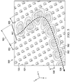
- FIG. 5 illustrates an example heat channel 550 formed by an example phononic bandgap structure 550 .
- This example illustrates a channel 551 that may be formed in IC 100 , referring back to FIG. 1 .
- a phononic bandgap structure may be formed within encapsulation material 123 by inserting a matrix of nodes 121 with a periodic spacing.
- the x-axis node spacing 554 is approximately equal to the y-axis node spacing 556 on one side of the channel.
- the node spacing 555 on the other side of channel 550 is approximately the same as node spacing 554 , 556 .
- the z-axis node spacing (not shown) is also approximately the same as node spacing 554 , 558 in this example.
- the node spacing 554 - 556 in this example may be selected to be approximately 2.5 nm, which is approximately one half of the wavelength of the center of the range of phononic wavelengths for 100 C heat, discussed above with regard to expressions (1)-(3).
- Channel 551 may be formed by not having any nodes within the region of the channel so that the channel region 551 has a width 553 that is larger than the wavelength of the desired bandgap. In this manner, acoustic energy in the form of heat energy phonons 552 that enter channel 551 may propagate through channel 551 as indicated by flow vector 528 .
- Phononic bandgap structure 551 may block a significant portion of the wave movement corresponding to heat energy in the 100 C temperature range and thereby cause it to propagate primarily through channel 551 .
- channel 551 is formed by omitting nodes within the channel region.
- a conductive layer may be formed through the phononic bandgap structure by omitting nodes within a layer region to form a node free conductive layer of encapsulation material within the phononic bandgap structure.
- channel 551 may be formed with a PBG structure lattice that has a bandgap at a different range of frequencies and will thereby allow heat phonons in the 100 C range to pass through.
- FIGS. 6A and 6B are cross sectional views of various example embodiments of heat channel 551 as shown in FIG. 5 that may be formed in IC 100 of FIG. 1 .
- FIG. 6A illustrates an example cross section of heat channel 551 that is more or less rectangular.
- FIG. 6B Illustrates an example cross section of heat channel 551 that is more or less square.
- Other cross sectional shapes may be implemented by selective omission of nodes. For example, a relatively wide channel may be implemented, a relatively tall channel may be implemented, a circular or oval cross section may be implemented, etc.
- FIG. 7 is a top view of an example QFN leadframe 700 that may be used to support IC 100 in FIG. 1 , for example.
- Other types of packages may use a leadframe strip that has a different known or later developed configuration.
- Lead frame strip 700 may include one or more arrays of individual lead frames.
- Lead frame strip 700 is typically fabricated from a copper sheet that is etched or stamped to form a pattern of thermal pads and contacts.
- Lead frame strip 700 may be plated with tin or another metal that will prevent oxidation of the copper and provide a lower contact surface that is easy to solder.
- An IC die may be attached to each individual lead frame.
- Each individual leadframe may include a thermal pad, such as thermal pads 104 .
- Each individual lead frame also includes a set of contacts that surround the thermal pad, such as contacts 105 .
- a sacrificial strip of metal connects all of the contacts together and provides mechanical support until a sawing process removes it.
- An IC die also referred to as a “chip,” is attached to each thermal pad during a packaging process. Wire bonding may then be performed to connect bond pads on each IC chip to respective contacts on the lead frame.
- the entire lead frame strip 700 may then be covered with a layer of mold compound using an additive process as described in more detail below to encapsulate the ICs. Lead frame strip 700 may then be singulated into individual packaged ICs by cutting along cut lines 728 , 729 .
- FIGS. 8A-8C are cross sectional views illustrating fabrication of the example IC package 100 of FIG. 1 .
- IC die 102 may be attached by die attach layer 842 to a thermal pad 104 of a leadframe that may be part of a leadframe strip similar to leadframe strip 700 shown in FIG. 7 that includes a set of contacts 105 .
- IC die 102 may be fabricated using known or later developed semiconductor processing techniques.
- IC die 102 may include an epitaxial (epi) layer 841 on the top surface in which are formed various semiconductor transistor devices and interconnects.
- One or more conductive layers may be formed on the epi layer and patterned into interconnect traces and bond pads 843 .
- a set of bond wires 106 may be attached to contacts 105 and bond pads 843 located on the surface of IC die 102 using known or later developed electrical connection techniques.
- IC package 100 is a quad-flat no-leads (QFN) package; however, in other embodiments various known or later developed packaging configurations, such as DFN, MLF, SON, dual inline packages (DIP), etc, may be fabricated using the techniques disclosed herein to form an encapsulated package with a thermal directing phononic bandgap structure included with the encapsulant material.
- FIG. 8B is a cross sectional view illustrating partial formation of encapsulation material 110 .
- Additive manufacturing processes are now being used in a number of areas.
- the international Association for Testing Materials (ASTM) has now promulgated ASTM F7292-12a “Standard Terminology for Additive Manufacturing Technologies” 2012 which is incorporated by reference herein.
- ASTM F2792 standard including: vat photopolymenzation, powder bed fusion, binder jetting, material jetting, sheet lamination, material extrusion, directed energy deposition.
- Hybrid processes may combine one or more of these seven basic processes with other manufacturing processes for additional processing flexibillty.
- Recent process advances allow additive manufacturing of 3D structures that have feature resolution of less than 10 nm, such as direct laser lithography, multi-photon lithograph, two-photon polymerization, etc.
- a vat photopolymerization process may be used in which leadframe strip and the ICs attached to it, such as IC die 102 , are lowered into a vat of liquid photopolymer resin.
- a light source such as a laser or projector, may then expose selected regions of the liquid photopolymer resin to initiate polymerization that converts exposed areas of the liquid resin to a solid.
- layers of encapsulant material 110 may be formed in selected shapes.
- encapsulant material that forms lattice 123 may be the same or different as the solid encapsulant material 110 .
- Nodes 121 may be formed with any selected lattice spacing.
- One or more heat channels 551 may be formed by varying the spacing of nodes 121 as the layers of encapsulant material are built up.
- FIG. 8C is a cross sectional view illustrating further partial formation of encapsulation material 110 around IC die 102 . Additional layers of liquid encapsulation material 110 have been exposed and converted to a solid. Selective exposure of the liquid resin allows lattice 123 to be formed with nodes 121 , as described with regard to FIG. 1 .
- the leadframe strip may be submerged in different vats at different times in order to allow different materials to form the nodes 121 within lattice 123 .
- Heat propagation vector 528 illustrates how heat produced by one portion of IC die 102 may be conducted to thermal pad 104 while this heat is blocked from reaching other portions of IC 102 by phononic bandgap structure that includes lattice 123 and periodically spaced nodes 121 .
- the leadframe strip may then be sawed or otherwise separated into individual encapsulated IC packages.
- encapsulation material 110 may be formed by other additive manufacturing processes.
- a powdered bed diffusion process may be used in which a powdered material is selectively consolidated by melting it together using a heat source such as a laser or electron beam.
- a material jetting process may be used in which droplets of material are deposited layer by layer to produce a stress directing encapsulation structure as described herein.
- bond wires 106 may require extra care to avoid disrupting the droplet streams.
- bond wires are not initially bonded to contacts 105 and bond pads 843 .
- a material jetting process may be used in which droplets of material are deposited layer by layer to produce a phononic bandgap structure as described herein.
- a conductive material may be deposited to form the bond wires between contacts 105 and bond pads 843 .
- a sintering process may be done by heating the encapsulated leadframe 700 assembly to further solidify the bond wires. The leadframe strip 700 may then be sawed or otherwise separated into individual encapsulated IC packages.
- IC die 102 is not initially attached to thermal pad 104 of a leadframe that may be part of a leadframe strip similar to leadframe strip 700 shown in FIG. 7 .
- a vat photopolymerization process may be used in which the leadframe strip is lowered into a vat of liquid photopolymer resin.
- a light source such as a laser or projector, may then expose selected regions of the liquid photopolymer resin to initiate polymerization that converts exposed areas of the liquid resin to a solid.
- layers of encapsulant material 110 may be formed in selected shapes.
- a phononic bandgap structure 126 as shown in FIG.
- a set of bond wires 106 may be attached to contacts 105 and bond pads 643 located on the surface of IC die 108 using known or later developed wire bonding techniques. Additional layers of resin may be exposed and hardened to form an additional phononic bandgap structure as described with regard to FIGS. 8A-8C , for example.
- the leadframe strip may then be sawed or otherwise separated into individual encapsulated IC packages.
- the phononic bandgap structure may be fabricated using a lattice material that includes filler particles diffused throughout the lattice material in place of the explicitly formed nodes as described above, such as nodes 121 .
- the filler particles are selected to have a size and material composition that will influence the characteristics of mechanical wave propagation, as described above.
- the filler material may be a polymer or other material that has different intrinsic material properties from the lattice material, in a similar manner as the difference between nodes 121 and lattice material 123 .
- the filler material may be hard, while in other embodiments the filler material may be soft or rubbery.
- multiple phononic bandgaps may be formed by using two or more types of fillers.
- a portion of the filler material may be a hard material, while another portion of the filler material may be a soft material.
- different size filler particle may be used in different regions or in a same region to form multiple bandgaps.
- a different number of filler particles per unit volume may be used in different regions to form different bandgaps.
- the filler dispersion will not be perfectly crystalline, but there will be a statistical mean separation of the filler particle that may lend itself to a bandgap based on the statistical mean separation distance of the filler particles.
- An additive manufacturing process may be used to encapsulate an IC die using two or more different polymers, such as one with filler particles and one without filler particles to form the PBG structures as described herein or other configurations of PBG structures.
- a selective molding process may be used in which one area of the encapsulation is molded with first polymer having either no filler particles or a first configuration of filler particles (size, material, number of particles per unit volume, etc.) and other areas are molded with a polymer having a different filler particle configuration to form a PBG structure as described herein or other configurations of PBG structures.
- FIG. 9 is a cross sectional view of another embodiment of an IC 900 with a phononic bandgap structure that includes lattice 123 that includes periodically spaced nodes 121 .
- a heat directing channel 951 is positioned to direct heat produced by one portion of IC 102 to another portion of IC 102 , as indicated by heat transfer vector 923 , while blocking the heat from other portions of IC 102 using a phononic bandgap structure as disclosed herein. This may be useful to maintain thermal balance of separate circuits within the IC, for example.
- FIG. 10A-10B are top and bottom views of an example IC package 1000 that includes a thermal directing phononic bandgap structure within the encapsulant material as described herein.
- IC 1000 is an illustration of a quad-flat no-leads (QFN) IC package that was encapsulated using additive manufacturing process to form thermal directing structures within the encapsulation material as described herein.
- FIG. 10A illustrates a top side
- FIG. 10B illustrates a bottom side of QFN package 1000 .
- Flat no-leads packages such as quad-flat no-leads (QFN) and dual-flat no-leads (DFN) physically and electrically connect integrated circuits to printed circuit boards.
- QFN quad-flat no-leads
- DNN dual-flat no-leads
- Flat no-leads also known as micro leadframe (MLF) and SON (small-outline no leads), is a surface-mount technology, one of several package technologies that connect ICs to the surfaces of PCBs without through-holes.
- Flat no-lead is a near chip scale plastic encapsulation package made with a planar copper lead frame substrate. Perimeter lands on the package bottom provide electrical connections to the PCB.
- Flat no-lead packages include an exposed thermal pad 1004 to improve heat transfer out of the IC (into the PCB). Heat transfer can be further facilitated by metal vias in the thermal pad.
- the QFN package is similar to the quad-flat package, and a ball grid array.
- QFN package 1000 includes a set of contacts 1005 arrayed around the perimeter of the package on the bottom side.
- Thermal pad 1004 has an exposed surface on the bottom side of QFN 1000 .
- An integrated circuit die (not shown) is mounted to the other side of thermal pad 1004 .
- the entire assembly is encapsulated in an encapsulation material 1010 using an additive manufacturing process as described herein to form a thermal directing phononic bandgap structure. While a QFN is illustrated in FIGS. 10A-10B , other embodiments may use other types of integrated circuit packages.
- FIG. 11 is a flow diagram illustrating fabrication of the example IC of FIG. 1 .
- an IC die may be attached to a thermal pad of a leadframe that includes a set of contacts as indicated at box 1102 .
- the IC die may be fabricated using known or later developed semiconductor processing techniques.
- the IC die may include an epitaxial (epi) layer on the top surface in which are formed various semiconductor transistor devices and interconnects.
- One or more conductive layers may be formed on the epi layer and patterned into interconnect traces and bond pads.
- a set of bond wires may be attached to the contacts and bond pads located on the surface of the IC die using known or later developed wire bonding techniques.
- a layer of thermal directing material that includes a phononic bandgap structure may be first formed on the thermal pad of the leadframe, as indicated at 1104 .
- the encapsulation material may be formed into a lattice with periodically spaced nodes that are filled with a different type of material to form a phononic bandgap structure.
- an additive manufacturing process may be used to create the lattice and fill the nodes in the lattice.
- An IC die may then be attached to the layer of stress directing encapsulation material, as indicated at 1106 .
- the IC die may then be completely encapsulated by an additive process to form a thermal directing structure within the encapsulation material as indicated at 1108 .
- a first portion of the encapsulation material may be solid and a second portion of the encapsulation material may include nodes filled with a second material to form a phononic bandgap structure.
- an additive manufacturing process may be used to create a lattice and fill the periodically spaced nodes in the lattice with a different type of material, or with several different types of material in different locations.
- the encapsulation process indicated at box 1108 may be done using a selective molding process in which one area of the encapsulation is molded with first polymer having either no filler particles or a first configuration of filler particles (size, material, number of particles per unit volume, etc.) and other areas are molded with a polymer having a different filler particle configuration diffused within the polymer to form a PBG structure as described herein or other configurations of PEG structures.
- IC packages may be formed in this manner.
- a quad-flat no-leads (QFN) package is illustrated in FIGS. 1-4 .
- various known or later developed packaging configurations such as DFN, MLF, SON, dual inline packages (DIP), etc, may be fabricated using the techniques disclosed herein to form an encapsulated package with stress directing material included with the encapsulant material.
- the lattice material may be relatively soft and the node material may be relatively hard.
- the lattice material may be relatively soft and the node material may be relatively hard.
- the node material may be air, another gas, or a vacuum, for example.
- a portion of the nodes may be formed with one kind of material, while another portion of the nodes may be formed with a different material.
- Several different types of material may be used to form different sets of nodes within the phononic bandgap structure to thereby tailor the performance of the phononic bandgap structure.
- a portion of the nodes may be formed with one lattice constant, while another portion of the nodes may be formed with a different lattice constant.
- Several different lattice constants may be used to form different sets of nodes within the phononic bandgap structure to thereby tailor the performance of the phononic bandgap structure.
- the nodes may be fabricated using various materials, such as: various polymers such as polyurethane, polyacrylates, etc., ceramic materials, metals, gases such as natural air, nitrogen etc. In some cases, a vacuum may be left and therefore no material would be used for some lattice nodes.
- a heat directing channel such as channel 551 as shown in FIG. 5 and channel 951 as shown in FIG. 9 or a heat deflecting layer such as layer 126 as shown in FIG. 1
- other embodiments may implement a wide layer in which a phononic bandgap is present.
- an IC die may be partially or completely surrounded by a phononic bandgap structure in the form of an enclosure that surrounds the IC, such as a box shaped or spherical shaped enclosure that is formed within the encapsulation material by selective placement of nodes within the encapsulation material such that heat is directed primarily to the thermal pad.
- the PBG structure may be symmetric in 3D, while in other embodiments the PBG structure may be asymmetric with different lattice spacing in different directions.
- the PBG structure may have a bandgap that is effective in all directions, while in other embodiments the PBG structure may have a bandgap in one direction but not in another direction, for example.
- Another example may demonstrate packages that are entirely encased in mold compound (such as a DIP).
- mold compound such as a DIP
- the only direct electrical contact with the board is through the pin legs. In this case it wouid be best to ensure that as much thermal energy directs down through the bottom portion of the mold compound and to the PCB in which it is mounted.
Landscapes
- Physics & Mathematics (AREA)
- Engineering & Computer Science (AREA)
- Acoustics & Sound (AREA)
- Computer Hardware Design (AREA)
- Microelectronics & Electronic Packaging (AREA)
- Power Engineering (AREA)
- Condensed Matter Physics & Semiconductors (AREA)
- General Physics & Mathematics (AREA)
- Multimedia (AREA)
- Structures Or Materials For Encapsulating Or Coating Semiconductor Devices Or Solid State Devices (AREA)
Abstract
Description
where ωk,s is the angular frequency of the phonons (or photons) in the state, kB is Boltzmann's constant, n is the reduced Planck's constant, and T is the temperature.
E=h×ν (2)
where h is Planck's constant, and ν is the frequency of the phonon.
lambda(λ)=v/ν (3)
Claims (12)
Priority Applications (3)
| Application Number | Priority Date | Filing Date | Title |
|---|---|---|---|
| US15/792,580 US10886187B2 (en) | 2017-10-24 | 2017-10-24 | Thermal management in integrated circuit using phononic bandgap structure |
| PCT/US2018/057351 WO2019084166A1 (en) | 2017-10-24 | 2018-10-24 | Thermal management in integrated circuit using phononic bandgap structure |
| US17/140,886 US12532772B2 (en) | 2017-10-24 | 2021-01-04 | Thermal management in integrated circuit using phononic bandgap structure |
Applications Claiming Priority (1)
| Application Number | Priority Date | Filing Date | Title |
|---|---|---|---|
| US15/792,580 US10886187B2 (en) | 2017-10-24 | 2017-10-24 | Thermal management in integrated circuit using phononic bandgap structure |
Related Child Applications (1)
| Application Number | Title | Priority Date | Filing Date |
|---|---|---|---|
| US17/140,886 Division US12532772B2 (en) | 2017-10-24 | 2021-01-04 | Thermal management in integrated circuit using phononic bandgap structure |
Publications (2)
| Publication Number | Publication Date |
|---|---|
| US20190122947A1 US20190122947A1 (en) | 2019-04-25 |
| US10886187B2 true US10886187B2 (en) | 2021-01-05 |
Family
ID=66170694
Family Applications (2)
| Application Number | Title | Priority Date | Filing Date |
|---|---|---|---|
| US15/792,580 Active 2038-04-11 US10886187B2 (en) | 2017-10-24 | 2017-10-24 | Thermal management in integrated circuit using phononic bandgap structure |
| US17/140,886 Active 2038-07-21 US12532772B2 (en) | 2017-10-24 | 2021-01-04 | Thermal management in integrated circuit using phononic bandgap structure |
Family Applications After (1)
| Application Number | Title | Priority Date | Filing Date |
|---|---|---|---|
| US17/140,886 Active 2038-07-21 US12532772B2 (en) | 2017-10-24 | 2021-01-04 | Thermal management in integrated circuit using phononic bandgap structure |
Country Status (2)
| Country | Link |
|---|---|
| US (2) | US10886187B2 (en) |
| WO (1) | WO2019084166A1 (en) |
Families Citing this family (4)
| Publication number | Priority date | Publication date | Assignee | Title |
|---|---|---|---|---|
| US10886187B2 (en) | 2017-10-24 | 2021-01-05 | Texas Instruments Incorporated | Thermal management in integrated circuit using phononic bandgap structure |
| US10557754B2 (en) | 2017-10-31 | 2020-02-11 | Texas Instruments Incorporated | Spectrometry in integrated circuit using a photonic bandgap structure |
| US20230194910A1 (en) * | 2021-12-22 | 2023-06-22 | Stmicroelectronics S.R.L. | Defect-based mems phononic crystal slab waveguide |
| US20240194629A1 (en) * | 2022-12-09 | 2024-06-13 | STATS ChipPAC Pte. Ltd. | Semiconductor Device and Method of Making a Semiconductor Package with Graphene for Die Attach |
Citations (62)
| Publication number | Priority date | Publication date | Assignee | Title |
|---|---|---|---|---|
| US3868764A (en) | 1973-11-09 | 1975-03-04 | Gen Motors Corp | Multiple magnetic alignment of semiconductor devices for bonding |
| US3868759A (en) | 1973-11-09 | 1975-03-04 | Gen Motors Corp | Magnetic pre-alignment of semiconductor device chips for bonding |
| US4974590A (en) | 1988-05-18 | 1990-12-04 | Olympus Optical Co., Ltd. | Ultrasonic probe for use in ultrasonic endoscope |
| US4999587A (en) | 1989-01-20 | 1991-03-12 | U.S. Philips Corp. | Waveguide oscillator tunable through integrated varactor diode and coupling probe |
| US5355577A (en) | 1992-06-23 | 1994-10-18 | Cohn Michael B | Method and apparatus for the assembly of microfabricated devices |
| US5500912A (en) | 1995-05-02 | 1996-03-19 | Motorola, Inc. | Holographic optical isolator utilizing opto-electronic transmitter and receiver disposed in a package |
| US5528074A (en) | 1994-02-03 | 1996-06-18 | Mitsubishi Denki Kabushiki Kaisha | Microwave semiconductor device and integrated circuit including microwave semiconductor devices |
| US5834320A (en) | 1995-06-05 | 1998-11-10 | Motorola, Inc. | Method of assembling a semiconductor device using a magnet |
| US6664615B1 (en) | 2001-11-20 | 2003-12-16 | National Semiconductor Corporation | Method and apparatus for lead-frame based grid array IC packaging |
| US20050224956A1 (en) | 2004-04-02 | 2005-10-13 | Chin-Li Kao | Chip package structure and chip packaging process |
| US6967347B2 (en) | 2001-05-21 | 2005-11-22 | The Regents Of The University Of Colorado | Terahertz interconnect system and applications |
| US6979105B2 (en) | 2002-01-18 | 2005-12-27 | Leysath Joseph A | Light device with photonic band pass filter |
| US20060054780A1 (en) | 2004-09-15 | 2006-03-16 | Raytheon Company | Multispectral imaging chip using photonic crystals |
| WO2006101577A2 (en) | 2005-03-16 | 2006-09-28 | Freescale Semiconductor, Inc. | Lead frame panel and a plurality of half-etched connection bars |
| US20070108545A1 (en) | 2005-11-17 | 2007-05-17 | Chua Janet B Y | Infrared-blocking encapsulant with organometallic colloids |
| US7228016B2 (en) | 2005-05-11 | 2007-06-05 | Hewlett-Packard Development Company, L.P. | Evanescent nanosensor using an optical resonator |
| US7305161B2 (en) | 2005-02-25 | 2007-12-04 | Board Of Regents, The University Of Texas System | Encapsulated photonic crystal structures |
| US20080112665A1 (en) | 2003-10-11 | 2008-05-15 | Beausoleil Raymond G | Photonic interconnect system |
| US20080218299A1 (en) | 2005-11-28 | 2008-09-11 | David Patrick Arnold | Method and Structure for Magnetically-Directed, Self-Assembly of Three-Dimensional Structures |
| US20090288852A1 (en) | 2008-05-20 | 2009-11-26 | Nec Electronics Corporation | Electronic device and method of manufacturing the same |
| US20100019247A1 (en) | 2006-10-05 | 2010-01-28 | Takahide Joichi | Light emitting device using gan led chip |
| US7733198B1 (en) | 2007-05-15 | 2010-06-08 | Sandia Corporation | Microfabricated bulk wave acoustic bandgap device |
| US20110001233A1 (en) | 2006-10-19 | 2011-01-06 | Teppei Iwase | Semiconductor device mounted structure and semiconductor device mounting method |
| US20110089815A1 (en) | 2009-10-15 | 2011-04-21 | Aurotek Corporation | Light-emitting device |
| US20110103632A1 (en) | 2009-10-30 | 2011-05-05 | Avago Technologies Wireless Ip (Singapore) Pte. Ltd. | Integrated acoustic horn and lead frame |
| US20110133597A1 (en) | 2009-12-05 | 2011-06-09 | Scannanotek Oy | Electromechanical systems, waveguides and methods of production |
| US20110221057A1 (en) | 2010-03-12 | 2011-09-15 | Stats Chippac, Ltd. | Semiconductor Device and Method of Forming Sacrificial Protective Layer to Protect Semiconductor Die Edge During Singulation |
| US8031012B2 (en) | 2008-02-08 | 2011-10-04 | Furukawa Electric Co., Ltd. | Optoelectronic oscillator and pulse generator |
| US8054145B2 (en) | 2008-04-30 | 2011-11-08 | Georgia Tech Research Corporation | Phononic crystal wave structures |
| US8094023B1 (en) | 2008-03-10 | 2012-01-10 | Sandia Corporation | Phononic crystal devices |
| US20120043628A1 (en) | 2010-08-19 | 2012-02-23 | Avago Technologies Wireless Ip (Singapore) Pte. Ltd. | Packaged device including a well for containing a die |
| US8143637B2 (en) | 2009-01-08 | 2012-03-27 | Renesas Electronics Corporation | Optically coupled device with an optical waveguide |
| US20120098611A1 (en) | 2007-12-17 | 2012-04-26 | Cymatics Laboratories Corp. | Integrated acoustic bandgap devices for energy confinement and methods of fabricating same |
| US20120154168A1 (en) | 2010-12-16 | 2012-06-21 | Baker Hughes Incorporated | Photonic crystal waveguide downhole communication system and method |
| US20130038174A1 (en) | 2011-08-08 | 2013-02-14 | Samsung Electro-Mechanics Co., Ltd. | Ultrasonic sensor |
| US20130228796A1 (en) | 2012-03-02 | 2013-09-05 | Cree, Inc. | High voltage semiconductor devices including electric arc suppression material and methods of forming the same |
| US8587182B2 (en) | 2006-10-24 | 2013-11-19 | Robert Bosch Gmbh | Ultrasonic transducer |
| US20140287703A1 (en) | 2013-03-19 | 2014-09-25 | Texas Instruments Incorporated | Integrated Circuit with Antenna for Dielectric Waveguide |
| US20140326902A1 (en) * | 2012-03-21 | 2014-11-06 | Charles George Tahan | Phoniton systems, devices, and methods |
| US9018074B2 (en) | 2009-10-01 | 2015-04-28 | Excelitas Canada, Inc. | Photonic semiconductor devices in LLC assembly with controlled molding boundary and method for forming same |
| US9070703B2 (en) | 2010-09-21 | 2015-06-30 | Texas Instruments Incorporated | High speed digital interconnect and method |
| US20150237423A1 (en) | 2013-03-21 | 2015-08-20 | Bichoy BAHR | Acoustic bandgap structures for integration of mems resonators |
| US9123737B2 (en) | 2010-09-21 | 2015-09-01 | Texas Instruments Incorporated | Chip to dielectric waveguide interface for sub-millimeter wave communications link |
| US20150295305A1 (en) | 2014-04-09 | 2015-10-15 | Texas Instruments Incorporated | Encapsulated Molded Package with Embedded Antenna for High Data Rate Communication Using a Dielectric Waveguide |
| US20160028367A1 (en) | 2014-07-25 | 2016-01-28 | Akoustis, Inc. | Single crystal acoustic resonator and bulk acoustic wave filter |
| US9343426B1 (en) | 2010-06-02 | 2016-05-17 | Maxim Integrated Products, Inc. | Use of device assembly for a generalization of three-dimensional metal interconnect technologies |
| US9450563B2 (en) | 2010-10-15 | 2016-09-20 | Commissariat A L'energie Atomique Et Aux Energies Alternatives | Acoustic wave bandpass filter comprising integrated acoustic guiding |
| US20160276311A1 (en) | 2014-09-26 | 2016-09-22 | Intel Corporation | Integrated circuit package having wirebonded multi-die stack |
| US20160327977A1 (en) | 2014-11-12 | 2016-11-10 | Intel Corporation | Flexible system-in-package solutions for wearable devices |
| US9583811B2 (en) | 2014-08-07 | 2017-02-28 | Infineon Technologies Ag | Transition between a plastic waveguide and a semiconductor chip, where the semiconductor chip is embedded and encapsulated within a mold compound |
| US20170084519A1 (en) | 2015-09-22 | 2017-03-23 | Freescale Semiconductor, Inc. | Semiconductor package and method of manufacturing same |
| US20170108655A1 (en) | 2011-12-28 | 2017-04-20 | Intel Corporation | Photonic package architecture |
| US9651718B2 (en) | 2014-01-27 | 2017-05-16 | Forelux Inc. | Photonic apparatus with periodic structures |
| WO2017111892A1 (en) | 2015-12-21 | 2017-06-29 | Intel Corporation | Integrated rf frontend structures |
| US20170186793A1 (en) | 2015-12-29 | 2017-06-29 | Viavi Solutions Inc. | Metal mirror based multispectral filter array |
| US20170253476A1 (en) | 2015-05-27 | 2017-09-07 | Texas Instruments Incorporated | Integrated Circuit Package with Sensor and Method of Making |
| US20170276870A1 (en) | 2010-11-30 | 2017-09-28 | Tshwane University Of Technology | Cmos based micro-photonic systems |
| US20170288123A1 (en) | 2014-09-19 | 2017-10-05 | Nihon Dempa Kogyo Co., Ltd. | Piezoelectric device and method for manufacturing the same |
| US20170292884A1 (en) | 2016-04-11 | 2017-10-12 | Nxp Usa, Inc. | Pressure-sensing integrated circuit device with diaphragm |
| US10062583B2 (en) | 2016-05-09 | 2018-08-28 | Qorvo Us, Inc. | Microelectronics package with inductive element and magnetically enhanced mold compound component |
| US10139564B1 (en) | 2015-01-28 | 2018-11-27 | National Technology & Engineering Solutions Of Sandia, Llc | Vertically integrated optoelectronics package for MEMS devices |
| US20190128735A1 (en) | 2017-10-31 | 2019-05-02 | Texas Instruments Incorporated | Spectrometry in Integrated Circuit Using a Photonic Bandgap Structure |
Family Cites Families (9)
| Publication number | Priority date | Publication date | Assignee | Title |
|---|---|---|---|---|
| SU1780469A1 (en) | 1990-02-12 | 1995-10-27 | Александровский завод им.50-летия СССР | Thermosetting plastic material for sealing semiconductor devices and integrated circuits |
| US6939505B2 (en) * | 2002-03-12 | 2005-09-06 | Massachusetts Institute Of Technology | Methods for forming articles having very small channels therethrough, and such articles, and methods of using such articles |
| US10643929B2 (en) | 2014-05-12 | 2020-05-05 | Texas Instruments Incorporated | Cantilevered leadframe support structure for magnetic wireless transfer between integrated circuit dies |
| US10358340B2 (en) * | 2016-04-28 | 2019-07-23 | Globalfoundries Singapore Pte. Ltd. | Integrated circuits having shielded MEMS devices and methods for fabricating shielded MEMS devices |
| US10886187B2 (en) | 2017-10-24 | 2021-01-05 | Texas Instruments Incorporated | Thermal management in integrated circuit using phononic bandgap structure |
| US10833648B2 (en) | 2017-10-24 | 2020-11-10 | Texas Instruments Incorporated | Acoustic management in integrated circuit using phononic bandgap structure |
| US10444432B2 (en) | 2017-10-31 | 2019-10-15 | Texas Instruments Incorporated | Galvanic signal path isolation in an encapsulated package using a photonic structure |
| US10497651B2 (en) | 2017-10-31 | 2019-12-03 | Texas Instruments Incorporated | Electromagnetic interference shield within integrated circuit encapsulation using photonic bandgap structure |
| US10371891B2 (en) | 2017-10-31 | 2019-08-06 | Texas Instruments Incorporated | Integrated circuit with dielectric waveguide connector using photonic bandgap structure |
-
2017
- 2017-10-24 US US15/792,580 patent/US10886187B2/en active Active
-
2018
- 2018-10-24 WO PCT/US2018/057351 patent/WO2019084166A1/en not_active Ceased
-
2021
- 2021-01-04 US US17/140,886 patent/US12532772B2/en active Active
Patent Citations (67)
| Publication number | Priority date | Publication date | Assignee | Title |
|---|---|---|---|---|
| US3868764A (en) | 1973-11-09 | 1975-03-04 | Gen Motors Corp | Multiple magnetic alignment of semiconductor devices for bonding |
| US3868759A (en) | 1973-11-09 | 1975-03-04 | Gen Motors Corp | Magnetic pre-alignment of semiconductor device chips for bonding |
| US4974590A (en) | 1988-05-18 | 1990-12-04 | Olympus Optical Co., Ltd. | Ultrasonic probe for use in ultrasonic endoscope |
| US4999587A (en) | 1989-01-20 | 1991-03-12 | U.S. Philips Corp. | Waveguide oscillator tunable through integrated varactor diode and coupling probe |
| US5355577A (en) | 1992-06-23 | 1994-10-18 | Cohn Michael B | Method and apparatus for the assembly of microfabricated devices |
| US5528074A (en) | 1994-02-03 | 1996-06-18 | Mitsubishi Denki Kabushiki Kaisha | Microwave semiconductor device and integrated circuit including microwave semiconductor devices |
| US5500912A (en) | 1995-05-02 | 1996-03-19 | Motorola, Inc. | Holographic optical isolator utilizing opto-electronic transmitter and receiver disposed in a package |
| US5834320A (en) | 1995-06-05 | 1998-11-10 | Motorola, Inc. | Method of assembling a semiconductor device using a magnet |
| US20060038168A1 (en) | 2001-05-21 | 2006-02-23 | Estes Michael J | Terahertz interconnect system and applications |
| US6967347B2 (en) | 2001-05-21 | 2005-11-22 | The Regents Of The University Of Colorado | Terahertz interconnect system and applications |
| US6664615B1 (en) | 2001-11-20 | 2003-12-16 | National Semiconductor Corporation | Method and apparatus for lead-frame based grid array IC packaging |
| US6979105B2 (en) | 2002-01-18 | 2005-12-27 | Leysath Joseph A | Light device with photonic band pass filter |
| US20080112665A1 (en) | 2003-10-11 | 2008-05-15 | Beausoleil Raymond G | Photonic interconnect system |
| US20050224956A1 (en) | 2004-04-02 | 2005-10-13 | Chin-Li Kao | Chip package structure and chip packaging process |
| US20060054780A1 (en) | 2004-09-15 | 2006-03-16 | Raytheon Company | Multispectral imaging chip using photonic crystals |
| US7305161B2 (en) | 2005-02-25 | 2007-12-04 | Board Of Regents, The University Of Texas System | Encapsulated photonic crystal structures |
| WO2006101577A2 (en) | 2005-03-16 | 2006-09-28 | Freescale Semiconductor, Inc. | Lead frame panel and a plurality of half-etched connection bars |
| US7228016B2 (en) | 2005-05-11 | 2007-06-05 | Hewlett-Packard Development Company, L.P. | Evanescent nanosensor using an optical resonator |
| US20070108545A1 (en) | 2005-11-17 | 2007-05-17 | Chua Janet B Y | Infrared-blocking encapsulant with organometallic colloids |
| US8138868B2 (en) | 2005-11-28 | 2012-03-20 | University Of Florida Research Foundation, Inc. | Method and structure for magnetically-directed, self-assembly of three-dimensional structures |
| US20080218299A1 (en) | 2005-11-28 | 2008-09-11 | David Patrick Arnold | Method and Structure for Magnetically-Directed, Self-Assembly of Three-Dimensional Structures |
| US20100019247A1 (en) | 2006-10-05 | 2010-01-28 | Takahide Joichi | Light emitting device using gan led chip |
| US20110001233A1 (en) | 2006-10-19 | 2011-01-06 | Teppei Iwase | Semiconductor device mounted structure and semiconductor device mounting method |
| US8587182B2 (en) | 2006-10-24 | 2013-11-19 | Robert Bosch Gmbh | Ultrasonic transducer |
| US7733198B1 (en) | 2007-05-15 | 2010-06-08 | Sandia Corporation | Microfabricated bulk wave acoustic bandgap device |
| US20120098611A1 (en) | 2007-12-17 | 2012-04-26 | Cymatics Laboratories Corp. | Integrated acoustic bandgap devices for energy confinement and methods of fabricating same |
| US8031012B2 (en) | 2008-02-08 | 2011-10-04 | Furukawa Electric Co., Ltd. | Optoelectronic oscillator and pulse generator |
| US8094023B1 (en) | 2008-03-10 | 2012-01-10 | Sandia Corporation | Phononic crystal devices |
| US8054145B2 (en) | 2008-04-30 | 2011-11-08 | Georgia Tech Research Corporation | Phononic crystal wave structures |
| US20090288852A1 (en) | 2008-05-20 | 2009-11-26 | Nec Electronics Corporation | Electronic device and method of manufacturing the same |
| US8143637B2 (en) | 2009-01-08 | 2012-03-27 | Renesas Electronics Corporation | Optically coupled device with an optical waveguide |
| US9018074B2 (en) | 2009-10-01 | 2015-04-28 | Excelitas Canada, Inc. | Photonic semiconductor devices in LLC assembly with controlled molding boundary and method for forming same |
| US20110089815A1 (en) | 2009-10-15 | 2011-04-21 | Aurotek Corporation | Light-emitting device |
| US20110103632A1 (en) | 2009-10-30 | 2011-05-05 | Avago Technologies Wireless Ip (Singapore) Pte. Ltd. | Integrated acoustic horn and lead frame |
| US20110133597A1 (en) | 2009-12-05 | 2011-06-09 | Scannanotek Oy | Electromechanical systems, waveguides and methods of production |
| US20110221057A1 (en) | 2010-03-12 | 2011-09-15 | Stats Chippac, Ltd. | Semiconductor Device and Method of Forming Sacrificial Protective Layer to Protect Semiconductor Die Edge During Singulation |
| US9343426B1 (en) | 2010-06-02 | 2016-05-17 | Maxim Integrated Products, Inc. | Use of device assembly for a generalization of three-dimensional metal interconnect technologies |
| US20120043628A1 (en) | 2010-08-19 | 2012-02-23 | Avago Technologies Wireless Ip (Singapore) Pte. Ltd. | Packaged device including a well for containing a die |
| US9070703B2 (en) | 2010-09-21 | 2015-06-30 | Texas Instruments Incorporated | High speed digital interconnect and method |
| US9123737B2 (en) | 2010-09-21 | 2015-09-01 | Texas Instruments Incorporated | Chip to dielectric waveguide interface for sub-millimeter wave communications link |
| US9450563B2 (en) | 2010-10-15 | 2016-09-20 | Commissariat A L'energie Atomique Et Aux Energies Alternatives | Acoustic wave bandpass filter comprising integrated acoustic guiding |
| US20170276870A1 (en) | 2010-11-30 | 2017-09-28 | Tshwane University Of Technology | Cmos based micro-photonic systems |
| US20120154168A1 (en) | 2010-12-16 | 2012-06-21 | Baker Hughes Incorporated | Photonic crystal waveguide downhole communication system and method |
| US20130038174A1 (en) | 2011-08-08 | 2013-02-14 | Samsung Electro-Mechanics Co., Ltd. | Ultrasonic sensor |
| US20170108655A1 (en) | 2011-12-28 | 2017-04-20 | Intel Corporation | Photonic package architecture |
| US20130228796A1 (en) | 2012-03-02 | 2013-09-05 | Cree, Inc. | High voltage semiconductor devices including electric arc suppression material and methods of forming the same |
| US20140326902A1 (en) * | 2012-03-21 | 2014-11-06 | Charles George Tahan | Phoniton systems, devices, and methods |
| US9373878B2 (en) | 2013-03-19 | 2016-06-21 | Texas Instruments Incorporated | Dielectric waveguide with RJ45 connector |
| US20140287703A1 (en) | 2013-03-19 | 2014-09-25 | Texas Instruments Incorporated | Integrated Circuit with Antenna for Dielectric Waveguide |
| US9306263B2 (en) | 2013-03-19 | 2016-04-05 | Texas Instruments Incorporated | Interface between an integrated circuit and a dielectric waveguide using a dipole antenna and a reflector |
| US20150237423A1 (en) | 2013-03-21 | 2015-08-20 | Bichoy BAHR | Acoustic bandgap structures for integration of mems resonators |
| US9651718B2 (en) | 2014-01-27 | 2017-05-16 | Forelux Inc. | Photonic apparatus with periodic structures |
| US20150295305A1 (en) | 2014-04-09 | 2015-10-15 | Texas Instruments Incorporated | Encapsulated Molded Package with Embedded Antenna for High Data Rate Communication Using a Dielectric Waveguide |
| US9647329B2 (en) | 2014-04-09 | 2017-05-09 | Texas Instruments Incorporated | Encapsulated molded package with embedded antenna for high data rate communication using a dielectric waveguide |
| US20160028367A1 (en) | 2014-07-25 | 2016-01-28 | Akoustis, Inc. | Single crystal acoustic resonator and bulk acoustic wave filter |
| US9583811B2 (en) | 2014-08-07 | 2017-02-28 | Infineon Technologies Ag | Transition between a plastic waveguide and a semiconductor chip, where the semiconductor chip is embedded and encapsulated within a mold compound |
| US20170288123A1 (en) | 2014-09-19 | 2017-10-05 | Nihon Dempa Kogyo Co., Ltd. | Piezoelectric device and method for manufacturing the same |
| US20160276311A1 (en) | 2014-09-26 | 2016-09-22 | Intel Corporation | Integrated circuit package having wirebonded multi-die stack |
| US20160327977A1 (en) | 2014-11-12 | 2016-11-10 | Intel Corporation | Flexible system-in-package solutions for wearable devices |
| US10139564B1 (en) | 2015-01-28 | 2018-11-27 | National Technology & Engineering Solutions Of Sandia, Llc | Vertically integrated optoelectronics package for MEMS devices |
| US20170253476A1 (en) | 2015-05-27 | 2017-09-07 | Texas Instruments Incorporated | Integrated Circuit Package with Sensor and Method of Making |
| US20170084519A1 (en) | 2015-09-22 | 2017-03-23 | Freescale Semiconductor, Inc. | Semiconductor package and method of manufacturing same |
| WO2017111892A1 (en) | 2015-12-21 | 2017-06-29 | Intel Corporation | Integrated rf frontend structures |
| US20170186793A1 (en) | 2015-12-29 | 2017-06-29 | Viavi Solutions Inc. | Metal mirror based multispectral filter array |
| US20170292884A1 (en) | 2016-04-11 | 2017-10-12 | Nxp Usa, Inc. | Pressure-sensing integrated circuit device with diaphragm |
| US10062583B2 (en) | 2016-05-09 | 2018-08-28 | Qorvo Us, Inc. | Microelectronics package with inductive element and magnetically enhanced mold compound component |
| US20190128735A1 (en) | 2017-10-31 | 2019-05-02 | Texas Instruments Incorporated | Spectrometry in Integrated Circuit Using a Photonic Bandgap Structure |
Non-Patent Citations (23)
| Title |
|---|
| "7 Families of Additive Manufacturing", According to ASTM F2792 Standards, Hybrid Manufacturing Technologies, pp. 1-2. |
| "Phonon", Wikipedia, available at https://en.wikipedia.org/wiki/Phonon on Aug. 2, 2017, pp. 1-9. |
| "Standard Terminology for Additive Manufacturing Technologies", ASTM International, F2792-12a,Sep. 9, 2013, pp. 1-3. |
| Benjamin Stassen Cook and Daniel Lee Revier, "Electromagnetic Interference Shield within Integrated Circuit Encapsulation Using Photonic Bandgap Structure", U.S. Appl. No. 15/799,757, filed Oct. 31, 2017, pp. 1-38. |
| Benjamin Stassen Cook and Daniel Lee Revier, "integrated Circuit with Dielectric Waveguide Connector Using Photonic Bandgap Structure", U.S. Appl. No. 15/800,042, filed Oct. 31, 2017, pp. 1-42. |
| Benjamin Stassen Cook and Daniel Lee Revier, "Spectrometry in Integrated Circuit Using a Photonic Bandgap Structure", U.S. Appl. No. 15/800,009, filed Oct. 31, 2017, pp. 1-41. |
| Benjamn Stassen Cook and Daniel Lee Revier, "Galvanic Signal Path Isolation in an Encapsulated Package Using a Photonic Structure", U.S. Appl. No. 15/799,140, filed Oct. 31, 2017, pp. 1-38. |
| Daniel Frederic Sievenpiper, "High-Impedance Electromagnetic Surfaces", 1999, University of California, pp. 1-162. |
| Daniel Lee Revier and Benjamin Stassen Cook, "Acoustic Management in Integrated Circuit Using Phononic Bandgap Structure", U.S. Appl. No. 15/792,591, filed Oct. 24, 2017, pp. 1-37. |
| Dr. Qin Hu, "Multiphoton Lithograpy Based 3D Micro/Nano Printing", EPSRC Centre for Innovative Manufacturing in Additive Manufacturing, pp. 1-30. |
| Hideo Kosaka et al, "Self-Collimating Phenomena in Photonic Crystals", Applied Physics Letters, vol. 74, No. 9, Mar. 1, 1999, pp. 1212-1214. |
| International Search Report for PCT/US2018/049135 dated Dec. 13, 2018. |
| International Search Report for PCT/US2018/049166 dated Dec. 13, 2018. |
| International Search Report for PCT/US2018/057351 dated Feb. 7, 2019. |
| International Search Report for PCT/US2018/057358 dated Feb. 7, 2019. |
| International Search Report for PCT/US2018/058478 dated Feb. 14, 2019. |
| International Search Report for PCT/US2018/058481 dated Feb. 7, 2019. |
| International Search Report for PCT/US2018/058487 dated Feb. 7, 2019. |
| International Search Report for PCT/US2018/058494 dated Feb. 21, 2019. |
| Mohammadi, et al. Complete phononic bandgaps and bandgap maps in two-dimensional silicon phononic crystal plates; Electronics Letters Aug. 2, 2017, vol. 43 No. 16. 2 pages. |
| Nagi Elabbasi, "Modeling Phononic Band Gap Materials and Structures", Comsol Blog, Feb. 10, 2016, pp. 1-7. |
| Optical Sensor-On-Chip ICs Simplify Handheld Spectrometer Design, available at https://www.digikey.com/en/articles/techzone/2017/jun/optical-sensor-on-chip-ics-simplify-handheld-spectrometer-design, Digi-Key Electronics, Jun. 28, 2017, pp. 1-6. |
| Yan Pennec and Bahram Djafari-Rouhani, "Fundamental Properties of Phononic Crystal", Chapter 2 in "Phononic Crystals", 2016, pp. 23-50. |
Also Published As
| Publication number | Publication date |
|---|---|
| US12532772B2 (en) | 2026-01-20 |
| US20210151357A1 (en) | 2021-05-20 |
| US20190122947A1 (en) | 2019-04-25 |
| WO2019084166A1 (en) | 2019-05-02 |
Similar Documents
| Publication | Publication Date | Title |
|---|---|---|
| US12532772B2 (en) | Thermal management in integrated circuit using phononic bandgap structure | |
| US10497651B2 (en) | Electromagnetic interference shield within integrated circuit encapsulation using photonic bandgap structure | |
| US10371891B2 (en) | Integrated circuit with dielectric waveguide connector using photonic bandgap structure | |
| US10833648B2 (en) | Acoustic management in integrated circuit using phononic bandgap structure | |
| US10444432B2 (en) | Galvanic signal path isolation in an encapsulated package using a photonic structure | |
| US10788367B2 (en) | Integrated circuit using photonic bandgap structure | |
| TWI764172B (en) | Package structure and manufacturing method thereof | |
| US10679955B2 (en) | Semiconductor package with heat-dissipating structure and method of manufacturing the same | |
| US7911047B2 (en) | Semiconductor device and method of fabricating the semiconductor device | |
| US20170133326A1 (en) | Wafer level fan-out with electromagnetic shielding | |
| TWI469301B (en) | Semiconductor multi-package module with wire contact interconnection in stacked package | |
| KR102600004B1 (en) | Semiconductor package | |
| KR102098592B1 (en) | Semiconductor package | |
| KR20050074961A (en) | Semiconductor stacked multi-package module having inverted second package | |
| US11127645B2 (en) | Grounding lids in integrated circuit devices | |
| US9818706B2 (en) | Moisture-resistant electronic component, notably microwave, and method for packaging such a component | |
| US8030138B1 (en) | Methods and systems of packaging integrated circuits | |
| US20140145348A1 (en) | Rf (radio frequency) module and method of maufacturing the same | |
| US10622270B2 (en) | Integrated circuit package with stress directing material | |
| KR100608366B1 (en) | Fine Pitch Ball Grid Array Package | |
| JP2023550701A (en) | Area shielding within the package of microelectronic devices | |
| CN216958002U (en) | Electronic component | |
| KR102060307B1 (en) | Semiconductor package | |
| JP2008270503A (en) | Semiconductor device and manufacturing method thereof |
Legal Events
| Date | Code | Title | Description |
|---|---|---|---|
| FEPP | Fee payment procedure |
Free format text: ENTITY STATUS SET TO UNDISCOUNTED (ORIGINAL EVENT CODE: BIG.); ENTITY STATUS OF PATENT OWNER: LARGE ENTITY |
|
| AS | Assignment |
Owner name: TEXAS INSTRUMENTS INCORPORATED, TEXAS Free format text: ASSIGNMENT OF ASSIGNORS INTEREST;ASSIGNORS:COOK, BENJAMIN STASSEN;REVIER, DANIEL LEE;REEL/FRAME:043951/0989 Effective date: 20171020 |
|
| STPP | Information on status: patent application and granting procedure in general |
Free format text: NON FINAL ACTION MAILED |
|
| STPP | Information on status: patent application and granting procedure in general |
Free format text: RESPONSE TO NON-FINAL OFFICE ACTION ENTERED AND FORWARDED TO EXAMINER |
|
| STPP | Information on status: patent application and granting procedure in general |
Free format text: NON FINAL ACTION MAILED |
|
| STPP | Information on status: patent application and granting procedure in general |
Free format text: RESPONSE TO NON-FINAL OFFICE ACTION ENTERED AND FORWARDED TO EXAMINER |
|
| STCF | Information on status: patent grant |
Free format text: PATENTED CASE |
|
| MAFP | Maintenance fee payment |
Free format text: PAYMENT OF MAINTENANCE FEE, 4TH YEAR, LARGE ENTITY (ORIGINAL EVENT CODE: M1551); ENTITY STATUS OF PATENT OWNER: LARGE ENTITY Year of fee payment: 4 |