US10739855B2 - Electronic device configured to collect biometric and amount of force data when a user touches a displayed image - Google Patents
Electronic device configured to collect biometric and amount of force data when a user touches a displayed image Download PDFInfo
- Publication number
- US10739855B2 US10739855B2 US16/017,438 US201816017438A US10739855B2 US 10739855 B2 US10739855 B2 US 10739855B2 US 201816017438 A US201816017438 A US 201816017438A US 10739855 B2 US10739855 B2 US 10739855B2
- Authority
- US
- United States
- Prior art keywords
- force
- electronic device
- sensor
- display
- input
- Prior art date
- Legal status (The legal status is an assumption and is not a legal conclusion. Google has not performed a legal analysis and makes no representation as to the accuracy of the status listed.)
- Active
Links
Images


Classifications
-
- G—PHYSICS
- G06—COMPUTING OR CALCULATING; COUNTING
- G06F—ELECTRIC DIGITAL DATA PROCESSING
- G06F3/00—Input arrangements for transferring data to be processed into a form capable of being handled by the computer; Output arrangements for transferring data from processing unit to output unit, e.g. interface arrangements
- G06F3/01—Input arrangements or combined input and output arrangements for interaction between user and computer
- G06F3/03—Arrangements for converting the position or the displacement of a member into a coded form
- G06F3/041—Digitisers, e.g. for touch screens or touch pads, characterised by the transducing means
- G06F3/044—Digitisers, e.g. for touch screens or touch pads, characterised by the transducing means by capacitive means
- G06F3/0445—Digitisers, e.g. for touch screens or touch pads, characterised by the transducing means by capacitive means using two or more layers of sensing electrodes, e.g. using two layers of electrodes separated by a dielectric layer
-
- G—PHYSICS
- G06—COMPUTING OR CALCULATING; COUNTING
- G06F—ELECTRIC DIGITAL DATA PROCESSING
- G06F21/00—Security arrangements for protecting computers, components thereof, programs or data against unauthorised activity
- G06F21/30—Authentication, i.e. establishing the identity or authorisation of security principals
- G06F21/31—User authentication
- G06F21/32—User authentication using biometric data, e.g. fingerprints, iris scans or voiceprints
-
- G—PHYSICS
- G06—COMPUTING OR CALCULATING; COUNTING
- G06F—ELECTRIC DIGITAL DATA PROCESSING
- G06F3/00—Input arrangements for transferring data to be processed into a form capable of being handled by the computer; Output arrangements for transferring data from processing unit to output unit, e.g. interface arrangements
- G06F3/01—Input arrangements or combined input and output arrangements for interaction between user and computer
- G06F3/016—Input arrangements with force or tactile feedback as computer generated output to the user
-
- G—PHYSICS
- G06—COMPUTING OR CALCULATING; COUNTING
- G06F—ELECTRIC DIGITAL DATA PROCESSING
- G06F3/00—Input arrangements for transferring data to be processed into a form capable of being handled by the computer; Output arrangements for transferring data from processing unit to output unit, e.g. interface arrangements
- G06F3/01—Input arrangements or combined input and output arrangements for interaction between user and computer
- G06F3/03—Arrangements for converting the position or the displacement of a member into a coded form
- G06F3/041—Digitisers, e.g. for touch screens or touch pads, characterised by the transducing means
- G06F3/044—Digitisers, e.g. for touch screens or touch pads, characterised by the transducing means by capacitive means
- G06F3/0447—Position sensing using the local deformation of sensor cells
-
- G06K9/00006—
-
- G06K9/00013—
-
- G—PHYSICS
- G06—COMPUTING OR CALCULATING; COUNTING
- G06V—IMAGE OR VIDEO RECOGNITION OR UNDERSTANDING
- G06V40/00—Recognition of biometric, human-related or animal-related patterns in image or video data
- G06V40/10—Human or animal bodies, e.g. vehicle occupants or pedestrians; Body parts, e.g. hands
- G06V40/12—Fingerprints or palmprints
- G06V40/13—Sensors therefor
-
- H—ELECTRICITY
- H03—ELECTRONIC CIRCUITRY
- H03K—PULSE TECHNIQUE
- H03K17/00—Electronic switching or gating, i.e. not by contact-making and –breaking
- H03K17/94—Electronic switching or gating, i.e. not by contact-making and –breaking characterised by the way in which the control signals are generated
- H03K17/96—Touch switches
- H03K17/9625—Touch switches using a force resistance transducer
-
- H—ELECTRICITY
- H03—ELECTRONIC CIRCUITRY
- H03K—PULSE TECHNIQUE
- H03K17/00—Electronic switching or gating, i.e. not by contact-making and –breaking
- H03K17/94—Electronic switching or gating, i.e. not by contact-making and –breaking characterised by the way in which the control signals are generated
- H03K17/96—Touch switches
- H03K17/964—Piezoelectric touch switches
-
- H—ELECTRICITY
- H03—ELECTRONIC CIRCUITRY
- H03K—PULSE TECHNIQUE
- H03K17/00—Electronic switching or gating, i.e. not by contact-making and –breaking
- H03K17/94—Electronic switching or gating, i.e. not by contact-making and –breaking characterised by the way in which the control signals are generated
- H03K17/965—Switches controlled by moving an element forming part of the switch
- H03K17/975—Switches controlled by moving an element forming part of the switch using a capacitive movable element
-
- G—PHYSICS
- G06—COMPUTING OR CALCULATING; COUNTING
- G06F—ELECTRIC DIGITAL DATA PROCESSING
- G06F2203/00—Indexing scheme relating to G06F3/00 - G06F3/048
- G06F2203/041—Indexing scheme relating to G06F3/041 - G06F3/045
- G06F2203/04105—Pressure sensors for measuring the pressure or force exerted on the touch surface without providing the touch position
-
- H—ELECTRICITY
- H03—ELECTRONIC CIRCUITRY
- H03K—PULSE TECHNIQUE
- H03K2217/00—Indexing scheme related to electronic switching or gating, i.e. not by contact-making or -breaking covered by H03K17/00
- H03K2217/94—Indexing scheme related to electronic switching or gating, i.e. not by contact-making or -breaking covered by H03K17/00 characterised by the way in which the control signal is generated
- H03K2217/96—Touch switches
- H03K2217/9607—Capacitive touch switches
- H03K2217/960755—Constructional details of capacitive touch and proximity switches
Definitions
- the described embodiments relate generally to force sensing. More particularly, the present embodiments relate to a force sensor in an input device.
- Many electronic devices include one or more input devices for receiving user inputs.
- Devices such as smart telephones, tablet computing devices, laptop computers, wearable communication and health devices, and navigation devices, and displays can include, or be connected to, an input device.
- an input device can provide information to a computing system regarding user interaction with a graphical user interface (GUI), such as selecting elements, returning to a home page, and other GUI features.
- GUI graphical user interface
- an input device can capture or receive biometric data associated with a user and provide such biometric data to a computing system.
- operation of an input device is binary.
- a key of a keyboard for example, is either pressed sufficiently to collapse a dome switch and generate an output signal, or it is not.
- An input button is either pressed sufficiently to close a switch and select an icon, or it is not.
- Binary inputs are inherently limited insofar as they can only occupy two states (present or absent, on or off, and so on). In some situations, it may be advantageous to also detect and measure the force of an input that is applied to an input device. In addition, when force is measured across a continuum of values, the detected force can function as a non-binary input.
- An input device can be included in an electronic device or operably connected to the electronic device using a wired or wireless connection.
- One or more force sensors in the input device is configured to detect a force input that is applied to a cover element.
- the cover element can be a portion of the housing of the electronic device or an input surface of the input device disposed in an aperture of the housing.
- the force sensor can employ any suitable force sensing technology, such as capacitive, piezoelectric, piezoresistive, ultrasonic, and magnetic force sensing technologies.
- the force sensor is a capacitive force sensor.
- the force sensor is formed with a first circuit layer that includes a first set of one or more electrodes and a second circuit layer that includes a second set of one or more electrodes.
- the second set of one or more electrodes is spaced apart from the first set of one or more electrodes by a compliant material (e.g., air, a silicone layer).
- Each electrode in the first set is aligned in at least one direction (e.g., vertically) with a respective electrode in the second set to produce one or more capacitors.
- the cover element When a force is applied to the cover element, the cover element bends or deflects which causes at least one electrode in the first set to move closer to a respective electrode in the second set.
- the capacitance of the capacitor formed by the two electrodes varies as the distance between the electrodes decreases.
- a force signal sensed from each capacitor represents a capacitance measurement of that capacitor.
- a processing device is configured to receive the force signal(s) and correlate the force signal(s) to an amount of force applied to the cover element.
- the input device includes a fingerprint sensor positioned below the cover element.
- the fingerprint sensor is configured to capture a fingerprint of a finger as the finger approaches or contacts the cover element.
- a force sensor is positioned below the fingerprint sensor and over a support element. The force sensor is configured to detect a force input applied to the cover element.
- an input device in another aspect, includes a cover element, one or more first force sensors positioned around a peripheral edge of the cover element, and a second force sensor positioned below the cover element.
- Each first force sensor is configured to detect a first force input applied to the cover element.
- the second force sensor is configured to detect a second force input applied to the cover element.
- the one or more first and the second force sensors can operate to detect force inputs in parallel, in series, or with a time offset.
- one force sensor can be used initially to detect an amount of applied force. As the amount of applied force increases, that force sensor reaches a maximum detectable force. At this point, the other force sensor may be used to detect the applied force.
- both the first and second force sensors can be used to detect a force input up to a given amount of force, and then one of the force sensors may be used to detect force inputs greater than the given amount of force.
- an input device for use with an electronic device can include a cover element, a fingerprint sensor positioned below the cover element, and a force sensor positioned below the fingerprint sensor and over a support element.
- the fingerprint sensor may be configured to capture a fingerprint of a finger as the finger approaches or contacts the cover element.
- the force sensor can be configured to detect a force input applied to the cover element.
- the input device may also include a compliant layer positioned below the cover element and around at least a portion of the fingerprint sensor.
- the input device can include additional components that receive one or more inputs from a user in addition to a force input.
- the input device includes a biometric sensor.
- the input device may include a switch element that detects a user input when a force input applied to the cover element exceeds a given amount of force. The switch element can generate or transmit a signal based on the detected user input, and a processing device can register the user input based on the signal received from the switch element.
- FIG. 1 shows one example of an electronic device that can include a force sensor in one or more input devices
- FIGS. 2A-2B show exploded views of a first input device that is suitable for use in the electronic device shown in FIG. 1 ;
- FIG. 3 shows a cross-sectional view of the input device shown in FIG. 2B when the input device is assembled
- FIG. 4 shows an exploded view of one example of the compliant layer shown in FIG. 3 ;
- FIG. 5 shows an exploded view of another example of the compliant layer shown in FIG. 3 ;
- FIG. 6 shows one example of a top view of the input device shown in FIG. 3 ;
- FIG. 7 shows another example of a top view of the input device shown in FIG. 3 ;
- FIG. 8 shows an exploded view of a second input device that is suitable for use in the electronic device shown in FIG. 1 ;
- FIG. 9 shows a cross-sectional view of the second input device shown in FIG. 8 when the input device is assembled
- FIG. 10 shows an exploded view of a third input device that is suitable for use in the electronic device shown in FIG. 1 ;
- FIG. 11 shows a cross-sectional view of the third input device shown in FIG. 10 when the input device is assembled.
- FIG. 12 shows a block diagram of one example of an electronic device that can include a force sensor in one or more input devices.
- cross-hatching in the figures is provided to distinguish the elements or components from one another.
- the cross-hatching is not intended to indicate a type of material or materials or the nature of the material(s).
- the following disclosure relates to an input device that includes one or more force sensors.
- the input device can be included in an electronic device and/or operably connected to an electronic device through a wired or wireless connection.
- the input device is an input button, but any suitable input device can include a force sensor.
- the force sensor includes two circuit layers in a stack of components that form the input device.
- the circuit layers are spaced apart from each other and a compliant material or air is disposed between the circuit layers.
- Each circuit layer includes a set of one or more electrodes, and each electrode in one set is aligned in at least one direction (e.g., vertically) with a respective electrode in the other set to produce one or more capacitors.
- the cover element bends or deflects which causes at least one electrode in one circuit layer to move closer to a respective electrode in the other circuit layer.
- the capacitance of the capacitor formed by the two electrodes varies as the distance between the electrodes changes.
- a force signal sensed from each capacitor represents a capacitance measurement of that capacitor.
- a processing device is configured to receive the force signal(s) and correlate the force signal(s) to an amount of force applied to the cover element.
- the force sensor is included in a compliant layer positioned at one or more locations within the input device.
- the compliant layer may be positioned around a periphery of the input button.
- the compliant layer may be formed with a compliant material disposed between two circuit layers.
- Each circuit layer includes a set of one or more electrodes, and each electrode in one set is aligned in at least one direction (e.g., vertically) with a respective electrode in the other set to produce one or more capacitors.
- the compliant material compresses or deforms, which causes at least one electrode in one circuit layer to move closer to a respective electrode in the other circuit layer.
- the capacitance of the capacitor formed by the two electrodes varies as the distance between the electrodes decreases.
- a processing device is configured to receive force signals from the capacitor(s) and correlate the force signals to an amount of applied force.
- the input device can include additional components that receive one or more inputs from a user in addition to a force input.
- the input device includes a biometric sensor.
- the biometric sensor is a fingerprint sensor that captures at least one fingerprint when a user's finger (or fingers) approaches and/or contacts the input surface.
- the input device may include a switch element that detects a user input when a force input exceeds a given amount of force.
- a switch element that detects a user input when a force input exceeds a given amount of force.
- Any suitable switch element can be used.
- an input device can include a dome switch that collapses when a force applied to an input surface exceeds a given magnitude. When collapsed, the dome switch completes a circuit that is detected by a processing device and recognized as an input (e.g., a selection of an icon, function, or application).
- force can function as a non-binary input.
- a force sensor can be configured to detect different amounts of force and the different amounts of force can be associated with different inputs to the electronic device, to an application, and/or to a function. For example, an increasing amount of force applied to an input device can be used to increase a level of sound output by a speaker in an electronic device.
- a first amount of force can be associated with a first input for an electronic device while a different second amount of force may be associated with a second input. For example, a first amount of force can be used to wake the electronic device from a sleep state while a larger second amount of force may be used to turn off the electronic device.
- increasing or decreasing amounts of force can be used to control an operation in a gaming application.
- an increasing amount of force may increase the speed of a moving object in a game (e.g., a car) while decreasing the amount of force can reduce the speed of the moving object.
- the absence of a force input may be used as a braking function to stop the movement of the object.
- FIG. 1 shows one example of an electronic device that can include a force sensor in one or more input devices.
- the electronic device 100 is implemented as a smart telephone.
- Other embodiments can implement the electronic device differently.
- an electronic device can be a laptop computer, a tablet computing device, a wearable computing device such as a smart watch or a health assistant, a digital music player, a display input device, a remote control device, and other types of electronic devices that include one or more input devices.
- the electronic device 100 includes a housing 102 surrounding a display 104 and an input device 106 .
- the input device 106 can be configured as an input/output device.
- the phrase “input device” is intended to include both input devices and input/output devices.
- the housing 102 can form an outer surface or partial outer surface for the internal components of the electronic device 100 , and may at least partially surround the display 104 and/or the input device 106 .
- the housing 102 can be formed of one or more components operably connected together, such as a front piece and a back piece. Alternatively, the housing 102 can be formed of a single piece operably connected to the display 104 .
- the display 104 can provide a visual output for the electronic device 100 and/or function to receive user inputs to the electronic device.
- the display 104 can be a multi-touch capacitive sensing touchscreen that can detect one or more user touch and/or force inputs.
- the display 104 may be substantially any size and may be positioned substantially anywhere on the electronic device 100 .
- the display 104 can be implemented with any suitable display, including, but not limited to, a multi-touch sensing touchscreen device that uses liquid crystal display (LCD) element, light emitting diode (LED) element, organic light-emitting display (OLED) element, or organic electro luminescence (OEL) element.
- LCD liquid crystal display
- LED light emitting diode
- OLED organic light-emitting display
- OEL organic electro luminescence
- the input device 106 can take the form of a home button, which may be a mechanical button, a soft button (e.g., a button that does not physically move but still accepts inputs), an icon or image on a display, and so on. Further, in some embodiments, the input device 106 can be integrated as part of a cover layer 108 and/or housing of the electronic device. Although not shown in FIG. 1 , the electronic device 100 can include one or more other input devices, such as a microphone, a speaker, other input buttons (e.g., volume, on-off), a camera, and one or more ports such as a network communication port and/or a power cord port.
- a home button which may be a mechanical button, a soft button (e.g., a button that does not physically move but still accepts inputs), an icon or image on a display, and so on.
- the input device 106 can be integrated as part of a cover layer 108 and/or housing of the electronic device.
- the electronic device 100 can include
- the cover layer 108 may be positioned over the front surface of the electronic device 100 . At least a portion of the cover layer 108 can receive touch and/or force inputs. In one embodiment, the cover layer 108 covers the display 104 and the input device 106 . Touch and force inputs can be received by the portions of the cover layer 108 that cover the display 104 and/or by the portion of the cover layer 108 that covers the input device 106 . In another embodiment, the cover layer 108 covers the display 104 but not the input device 106 . In such embodiments, the input device 106 can be positioned in an opening or aperture 110 formed in the cover layer 108 . The input device 106 can receive touch and/or force inputs as well as the portion of the cover layer 108 that covers the display 104 .
- the input surface of the input device may be integrated into the housing 102 .
- the input surface may be part of the housing 102 with the force sensor and other components of the input device disposed below the housing 102 .
- a depression or recess in the housing 102 may indicate the location of an input device (e.g., an input button).
- a force sensor or sensors can be included in one or more locations of the electronic device 100 .
- one or more force sensors may be included in the input device 106 (and/or in other input buttons or areas of the electronic device 100 ).
- the force sensor(s) can be used to measure an amount of force and/or a change in force that is applied to the input device 106 .
- one or more force sensors can be positioned under at least a portion of the housing 102 to detect a force and/or a change in force that is applied to the housing 102 .
- one or more force sensors may be included in a display stack of the display 104 .
- the force sensor(s) can be used to measure an amount of force and/or a change in force that is applied to the display 104 or to a portion of the display 104 .
- Embodiments described herein include one or more force sensors in the input device 106 .
- the input device 106 may also include additional operations or devices, such as a biometric sensor, other circuitry, support elements, and/or a switch element.
- the various components and devices can be arranged in a device stack that is positioned below a cover element.
- FIGS. 2A-2B show exploded views of a first input device suitable for use in the electronic device shown in FIG. 1 .
- the input device stack 200 includes a cover element 202 and a trim 204 .
- the trim 204 completely surrounds the sides of the cover element 202 and the perimeter of the top surface of the cover element 202 .
- Other embodiments are not limited to this configuration.
- the sides and/or top surface of the cover element 202 can be partially surrounded by the trim 204 .
- the trim 204 can be omitted in other embodiments.
- Both the cover element 202 and the trim 204 can be formed with any suitable opaque, transparent, and/or translucent material.
- the cover element 202 can be made of glass, plastic, or sapphire and the trim 204 may be made of a metal or plastic.
- one or more additional layers can be positioned below the cover element 202 .
- an opaque ink layer can be disposed below the cover element 202 when the cover element 202 is made of a transparent material. The opaque ink layer can conceal the other components in the input device stack 200 so that the other components are not visible through the transparent cover element 202 .
- a first circuit layer 206 can be disposed below the cover element 202 .
- Any suitable circuit layer may be used.
- the first circuit layer 206 may be a circuit board or a flexible circuit.
- the first circuit layer 206 can include one or more circuits, signal lines, and/or integrated circuits.
- the first circuit layer 206 includes a biometric sensor 208 .
- Any suitable type of biometric sensor can be used.
- the biometric sensor is a capacitive fingerprint sensor that captures at least one fingerprint when a user's finger (or fingers) approaches and/or contacts the cover element 202 .
- the first circuit layer 206 may be attached to the bottom surface of the cover element 202 with an adhesive layer 210 .
- Any suitable adhesive can be used for the adhesive layer.
- a pressure sensitive adhesive layer may be used as the adhesive layer 210 .
- a compliant layer 212 is disposed below the first circuit layer 206 .
- the compliant layer 212 includes an opening 214 formed in the compliant layer 212 .
- the opening 214 exposes the top surface of the first circuit layer 206 and/or the biometric sensor 208 when the device stack 200 is assembled.
- the compliant layer 212 is positioned around an interior perimeter of the trim 204 and/or around a peripheral edge of the cover element 202 (see FIG. 3 ). Although depicted in a circular shape, the compliant layer 212 can have any given shape and/or dimensions, such as a square or oval.
- the compliant layer 212 is shown as a continuous compliant layer in FIG. 2 , but other embodiments are not limited to this configuration.
- the compliant layer 212 does not include the opening 214 and the compliant layer 212 extends across at least a portion of the input device stack 200 .
- the compliant layer 212 may extend across the bottom surface of the cover element 202 , the bottom surface of the first circuit layer 206 , or a portion of the bottom surface of the cover element 202 (e.g., around the peripheral edge of the cover element) and the bottom surface of the first circuit layer 206 .
- a second circuit layer 218 is positioned below the first circuit layer 206 .
- a flexible circuit and a circuit board are examples of a circuit layer that can be used in the second circuit layer 218 .
- the second circuit layer 218 can include a first circuit section 220 and a second circuit section 222 .
- the first and second circuit sections 220 , 222 can be electrically connected one another other.
- the first circuit section 220 can include a first set of one or more force sensor components that are included in a force sensor. In some embodiments, the first circuit section 220 can be electrically connected to the first circuit layer 206 . For example, when the first circuit layer 206 includes a biometric sensor 208 , the biometric sensor 208 may be electrically connected to the first circuit section 220 of the second circuit layer 218 .
- the second circuit section 222 can include additional circuitry, such as signal lines, circuit components, integrated circuits, and the like.
- the second circuit section 222 may include a board-to-board connector 224 to electrically connect the second circuit layer 218 to other circuitry in the electronic device.
- the second circuit layer 218 can be operably connected to a processing device using the board-to-board connector 224 .
- the second circuit layer 218 may be operably connected to circuitry that transmits signals (e.g., sense signals) received from the force sensor component(s) in the first circuit section 220 to a processing device.
- the second circuit layer 218 may be operably connected to circuitry that provides signals (e.g., drive signals, a reference signal) to the one or more force sensor components in the first circuit section 220 .
- the first circuit section 220 of the second circuit layer 218 may be attached to the bottom surface of the first circuit layer 206 using an adhesive layer 216 .
- a die attach film may be used to attach the first circuit section 220 to the bottom surface of the first circuit layer 206 .
- a third circuit layer 226 is disposed below the first circuit section 220 of the second circuit layer 218 .
- the third circuit layer 226 may include a second set of one or more force sensor components that are included in a force sensor.
- the third circuit layer 226 is supported by and/or attached to a support element 228 .
- the support element 228 is attached to the trim 204 to produce an enclosure for the other components in the device stack 200 .
- the support element 228 may be attached to the trim 204 using any suitable attachment mechanism.
- the force sensor can use any suitable force sensing technology.
- Example sensing technologies include, but are not limited to, capacitive, piezoelectric, piezoresistive, ultrasonic, and magnetic.
- the force sensor is a capacitive force sensor.
- the first set of one or more force sensor components can include a first set of one or more electrodes 230 and the second set of one or more force sensor components a second set of one or more electrodes 232 .
- each electrode in the first and second sets of one or more electrodes 230 , 232 can have any given shape (e.g., rectangles, circles).
- the one or more electrodes in the first and second sets 230 , 232 may be arranged in any given pattern (e.g., one or more rows and one or more columns).
- FIGS. 2A and 2B show two electrodes in the first and second sets of one or more electrodes 230 , 232 .
- the first and second sets of one or more electrodes 230 , 232 may each be a single electrode or multiple discrete electrodes.
- the second set of one or more electrodes comprises multiple discrete electrodes.
- the second set of one or more electrodes can be a single electrode and the first set includes multiple discrete electrodes.
- both the first and second sets of one or more electrodes may each include multiple discrete electrodes.
- Each electrode in the first set of one or more electrodes 230 is aligned in at least one direction (e.g., vertically) with a respective electrode in the second set of one or more electrodes 232 to produce one or more capacitors.
- a force input is applied to the cover element 202 (e.g., the input surface of the input device)
- at least one electrode in the first set 230 moves closer to a respective electrode in the second set 232 , which varies the capacitance of the capacitor(s).
- a force signal sensed from each capacitor represents a capacitance measurement of that capacitor.
- a processing device (not shown) is configured to receive the force signal(s) and correlate the force signal(s) to an amount of force applied to the cover element 202 .
- the force sensor is configured to detect a range of force inputs with at least two force inputs representing different user inputs. For example, a first force input can select an icon and a different second force input can turn off an electronic device. Additionally or alternatively, in another example a first force input can produce a scrolling operation that scrolls at a first speed and a different second force input may produce a scrolling operation that scrolls at a different second speed (e.g., faster). Additionally or alternatively, in some embodiments the force sensor can replace other components in an input device. For example, a force sensor may replace a switch element.
- a switch element 234 can be positioned below the support element 228 .
- the switch element 234 registers a user input when a force input applied to the cover element 202 exceeds a given amount of force (e.g., a force threshold associated with closing the distance between the first circuit section 220 and the third circuit layer 226 ; see FIG. 3 ).
- a force threshold associated with closing the distance between the first circuit section 220 and the third circuit layer 226 ; see FIG. 3 .
- Any suitable switch element can be used.
- the switch element 234 may be a dome switch that collapses when the force input applied to the cover element 202 exceeds the force threshold. When collapsed, the dome switch completes a circuit that is detected by a processing device and recognized as a user input (e.g., a selection of an icon, function, or application).
- the dome switch is arranged such that the apex of the collapsible dome is proximate to the bottom surface of the support plate 228 .
- the base of the collapsible dome can be proximate to the bottom surface of the support plate 228 .
- FIG. 3 shows a cross-sectional view of the input device shown in FIG. 2B when the input device is assembled.
- the trim 204 is positioned in an aperture formed in the housing of an electronic device (e.g., aperture 1010 in housing 102 in FIG. 1 ).
- the trim 204 includes a shelf 300 that extends inward from the trim 204 toward the input device stack.
- the compliant layer 212 is positioned between the shelf 300 and a peripheral edge of the cover element 202 .
- the compliant layer 212 may be made of any suitable material or materials.
- the compliant layer 212 is a silicone layer.
- the compliant layer 212 can be formed as shown in FIG. 4 .
- a compliant material 400 may be positioned between two intermediate layers 402 , 404 .
- An exterior layer 406 , 408 can be disposed over each intermediate layer 402 , 404 .
- the compliant material 400 may be formed with silicone, the intermediate layers 402 , 404 can be formed with a polyimide, and the exterior layers 406 , 408 may be formed with a heat activated film.
- FIG. 5 shows an exploded view of another example of the compliant layer shown in FIG. 3 .
- a compliant material 500 may be positioned between two circuit layers 502 , 504 .
- a first set of one or more force sensor components 506 is formed in or on the first circuit layer 502 .
- a second set of one or more force sensor components 508 is formed in or on the second circuit layer 504 .
- the first and second sets of one or more force sensor components each include one or more electrodes.
- each circuit layer 502 , 504 can be formed with silicone
- each circuit layer 502 , 504 can be formed with a flexible circuit that includes a set of one or more electrodes (e.g., 230 , 232 )
- each exterior layer 510 , 512 may be formed with a heat activated film.
- the circuit layers 502 , 504 allow the compliant layer 212 to act as a second force sensor.
- the second force sensor can be used in series, concurrently, or offset in time with the first force sensor formed by the second and third circuit layers 218 , 226 .
- one force sensor e.g., the second force sensor
- the force sensor can be used initially to detect an amount of applied force. As the amount of applied force increases, the force sensor reaches a maximum detectable force. At this point, the other force sensor (e.g., the first force sensor) may be used to detect the applied force.
- both the first and second force sensors can be used to detect force inputs up to a given amount of force, and then one of the force sensors may be used to detect force inputs greater than the given amount of force.
- the second capacitive force sensor operates similarly to the first capacitive force sensor.
- Each electrode in the first set of one or more electrodes 506 is aligned in at least one direction (e.g., vertically) with a respective electrode in the second set of one or more electrodes 508 to produce one or more capacitors 514 .
- the capacitance of at least one capacitor 514 can vary when a user applies a force to the cover element 202 because the electrodes in at least one capacitor 514 move closer together.
- a user can apply the force to the cover element 202 with a device, such as a stylus, or with a body part (e.g., one or more fingers).
- Force signals produced by the one or more capacitors 514 represent capacitance measurement(s) of the one or more capacitors 514 .
- a processing device that receives the force signal(s) is configured to correlate the force signal(s) to an amount of force applied to the cover element 202 .
- the compliant layer 212 can seal the interface between the bottom surface of the cover element 202 and the top surface of the shelf 300 .
- the compliant layer 212 may act as an environmental seal that prevents contaminants, such as water, chemicals, and dirt, from entering the input device stack and/or the electronic device.
- the first circuit layer 206 (with the biometric sensor 208 ) is positioned below the cover element 202 , and the second circuit layer 218 is positioned below the first circuit layer 206 .
- the third circuit layer 226 is disposed below the second circuit layer 218 and over the support element 228 .
- the support element 228 is attached to the trim 204 using fasteners 302 . Any suitable type of fastener may be used, such as a screw, solder, and an adhesive.
- a gap 304 is defined between the second and third circuit layers 218 , 226 .
- the gap 304 is formed based at least in part by the downward step 305 in the support element 228 .
- the electrode(s) in the first and second sets of one or more electrodes form a capacitor.
- the gap 304 separates the electrodes in the first and second sets and includes the dielectric material for the capacitor(s). Any suitable dielectric material can be used.
- the dielectric material can include, but is not limited to, air, a compliant gel, a compliant material, and/or one or more compliant elements disposed between the second and third circuit layers 218 , 226 .
- the cover element 202 and the trim 204 are fixed in position and do not move when a force is applied to the cover element 202 .
- the gap 304 permits the first circuit section 220 of the second circuit layer 218 to bend or deflect relative to the third circuit layer 226 when a force input is applied to the cover element 202 . This deflection varies the capacitance of one or more capacitors formed by the electrode(s) in the first circuit section 220 and third circuit layer 226 .
- additional circuitry and/or components may be attached and electrically connected to the second circuit layer 218 .
- a second integrated circuit 306 may be attached and electrically connected to the second circuit layer 218 .
- some additional circuitry may be encapsulated with a protective and/or insulting material 308 .
- the protective and/or insulating material 308 can filter noise from signals and circuitry in or on the second circuit layer 218 .
- the protective and/or insulating material 308 extends into an opening 236 formed in the support element 228 (see FIGS. 2A-2B ).
- a switch element 234 may be disposed below the support element 228 .
- the switch element 234 is depicted as a dome switch in FIG. 3 .
- the dome switch is arranged such that the base of the collapsible dome is proximate (e.g., attached) to the bottom surface of the support plate 228 .
- the apex of the collapsible dome may be proximate to, or in contact with, the bottom surface of the support plate 228 .
- FIG. 6 shows one example of a top view of the input device shown in FIG. 3 .
- the cover element 202 is omitted for clarity.
- the compliant layer 212 is formed as a continuous ring of compliant material that is positioned around the trim 204 (e.g., over shelf 300 of the trim 204 in FIG. 3 ).
- the compliant layer 212 may act as an environmental seal that prevents contaminants, such as water, chemicals, and dirt, from entering the input device stack and/or the electronic device.
- the corners 600 of the first circuit layer 206 (and/or the biometric sensor 208 ) may be notched to ensure the compliant layer 212 meets all standards for an environmental seal, such as a width requirement.
- the adhesive layer 210 is used to attach the first circuit layer 206 to the bottom surface of the cover element. Additionally, in some embodiments the second circuit layer 218 extends beyond the trim 204 and folds over itself to provide a circuit layer. For example, in some embodiments the third circuit layer 226 can be a part of the second circuit layer 218 that is folded over and positioned over the support element 228 .
- FIG. 7 shows another example of a top view of the input device shown in FIG. 3 .
- the compliant layer 212 is formed as discrete compliant layers 700 , 702 , 704 , 706 that are positioned at different locations around the trim 204 (e.g., over the shelf 300 in FIG. 3 ).
- the edges and corners of the first circuit layer 206 do not have to be modified or notched.
- the dimensions or size of the biometric sensor can be larger when discrete compliant layers are included in the input device. Although only four discrete compliant layers are shown in FIG. 7 , other embodiments can include any number of discrete compliant layers.
- An environmental seal can be formed with a material that fills the gaps 708 around the discrete compliant layers 700 , 702 , 704 , 706 and between the cover element 202 and the trim 204 .
- the material is water and chemical resistance and is compliant relative to the discrete compliant layers 700 , 702 , 704 , 706 .
- the environmental seal prevents contaminants such as liquid, dirt, and dust from entering the input device stack and/or the electronic device.
- a glue may be used to form the environmental seal.
- FIG. 8 shows an exploded view of a second input device that is suitable for use in the electronic device shown in FIG. 1 .
- the input device stack 800 is inverted in FIG. 8 , with the cover element 802 shown at the bottom of the figure.
- one or more additional layers 804 can be positioned below the cover element 802 .
- the additional layer(s) can include, but are not limited to, an ink layer and/or an adhesive layer.
- a first circuit layer 806 may be positioned below the cover element 802 (or below the additional layer(s) 804 when included in the input device stack 800 ).
- the first circuit layer 806 may be any suitable circuit layer, such as a circuit board or a flexible circuit.
- the first circuit layer 806 includes a biometric sensor 808 formed on or in the first circuit layer 806 and operably connected to the first circuit layer 806 .
- the biometric sensor 808 is a fingerprint sensor.
- the first circuit layer 806 and the biometric sensor 808 can be molded into a plastic mold or enclosure 809 .
- the plastic enclosure 809 can serve as an environmental seal for the first circuit layer 806 and the biometric sensor 808 .
- a support layer 810 can be disposed below the first circuit layer 806 .
- the support layer 810 may include circuitry 812 , 814 , 816 electrically connected to a second circuit layer 818 .
- the second circuit layer 818 may be a flexible circuit or a circuit board.
- the second circuit layer 818 is a flexible circuit that includes a second circuit layer tail 820 that extends into the opening 822 in the trim 824 .
- circuitry 812 , 814 , and/or 816 may be electrically connected to contacts 826 , 828 on the first circuit layer 806 . In some embodiments, at least a portion of circuitry 812 may extend into the opening 830 in the trim 824 .
- the circuitry 812 , 814 , and/or 816 may be encapsulated with an insulating and/or protective material (not shown).
- a compliant layer 832 is positioned below the support layer 810 .
- the compliant layer 832 includes an opening 833 that permits the compliant layer 832 to reside around the interior perimeter of the trim 824 and/or around a peripheral edge of the cover element 802 .
- the compliant layer 832 can have any given shape and/or dimensions, such as a square or oval.
- the compliant layer 832 may include multiple discrete compliant layers in the device stack 800 . Additionally or alternatively, the compliant layer 832 may not include the opening 833 such that the compliant layer 832 extends across at least a portion of the input device stack 800 .
- the compliant layer 832 may extend across the bottom surface of the cover element 802 , the bottom surface of the first circuit layer 806 , or a portion of the bottom surface of the cover element 802 (e.g., around the peripheral edge of the cover element) and the bottom surface of the first circuit layer 806 .
- the compliant layer 832 may be made of any suitable material or combination of materials.
- the compliant layer 832 can be formed with silicone.
- the compliant layer 832 can be constructed as shown in FIG. 4 or in FIG. 5 .
- the compliant layer 832 may function as an additional force sensor when the compliant layer 832 is constructed as shown in FIG. 5 .
- a third circuit layer 834 may be disposed below the support layer 810 .
- the third circuit layer 834 may be any suitable circuit layer, such as a circuit board or a flexible circuit.
- the third circuit layer 834 is a flexible circuit that includes a circuit layer tail 836 that extends into the opening 822 of the trim 824 .
- the trim 824 forms a container or holder in that the trim 824 includes a cavity defined by the bottom surface and sides of the trim 824 .
- the cover element 802 , the optional one or more additional layers 804 , the first circuit layer 806 , the support layer 810 , the second circuit layer 818 , the compliant layer 832 , and the third circuit layer 834 all reside within the cavity of the trim 824 .
- the bottom surface of the trim 824 acts as a support element for the third circuit layer 834 .
- the second and third circuit layers 818 , 834 each include a set of one or more force sensor components that are included in a force sensor.
- the force sensor can use any suitable sensing technology.
- the second and third circuit layers 818 , 834 each include one or more electrodes (not shown) that are used to sense changes in capacitance.
- the electrode(s) may be configured as shown and described in conjunction with FIGS. 2A-2B .
- a processing device receives force signals that represent capacitance values for the one or more capacitors formed by the electrode(s).
- a processing device receives force signals from the one or more capacitors and correlates the force signals into an amount of force that is applied to the cover element 802 .
- FIG. 9 shows a cross-sectional view of the second input device shown in FIG. 8 when the input device is assembled.
- the trim 824 is positioned in an aperture 900 formed in the housing 902 of an electronic device (e.g., housing 102 in FIG. 1 ).
- the cover element 802 Disposed within the trim 824 are the cover element 802 and the various layers of the input device stack 800 (e.g., the optional additional layer(s) 804 , the first circuit layer 806 , the support layer 810 , the second circuit layer 818 , the third circuit layer 834 , and the compliant layer 832 ).
- the second circuit layer tail 820 and the third circuit layer tail 836 extend out of the trim 824 through the opening 822 .
- the second and third circuit layer tails 820 , 836 can be operably connected to other circuitry, such as a processing device and/or signal generator.
- the second and third circuit layers 818 , 834 can be included in a force sensor.
- the second and third circuit layers 818 , 834 may each include a set of one or more force sensor components that are included in the force sensor.
- the second and third circuit layers 818 , 834 can each include a set of one or more electrodes (not shown).
- the one or more electrodes may be configured as shown and described in conjunction with FIGS. 2A-2B .
- the second and third circuit layer tails 820 , 836 may be operably connected to one or more processing devices (not shown).
- the force signals received from the force sensor e.g., capacitor(s) formed with electrodes
- drive or reference signals may be transmitted to the force sensor (e.g., capacitor(s) formed with electrodes) using the other circuit layer tail (e.g., third circuit layer tail 836 ).
- a gap 912 is defined between the second and third circuit layers 818 , 834 .
- the gap 912 includes the dielectric material for the capacitor(s) that is formed with the sets of one or more electrodes in the second and third circuit layers 818 , 834 .
- the gap 912 permits the second circuit layer 818 to move, bend, or deflect relative to the third circuit layer 834 when a force input is applied to the cover element 802 . This deflection varies the capacitance of one or more capacitors formed by the electrode(s) in the second and third circuit layers 818 , 834 .
- the second circuit layer 818 is electrically connected to the first circuit layer 806 with bonding wires 904 .
- the bonding wires 904 may be covered or encapsulated by a protective and/or insulating material 906 .
- a seal 908 can be disposed between the trim 824 and the housing 902 .
- the seal is an O-ring that is positioned within an indentation 910 formed along an exterior surface of the trim 824 .
- the seal 908 can function as an environmental seal that prevents contaminants such as liquid, dirt, and dust from entering the input device stack and/or the electronic device.
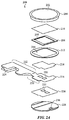
- FIG. 10 shows an exploded view of a third input device that is suitable for use in the electronic device shown in FIG. 1 .
- the input device stack 1000 is shown inverted with the cover element 1002 shown at the bottom of the figure.
- one or more additional layers 1004 can be positioned below the cover element 1002 .
- the additional layer(s) can include, but are not limited to, an ink layer and/or an adhesive layer.
- a first circuit layer 1006 may be positioned below the cover element 1002 (or below the additional layer(s) 1004 when included in the input device stack 1000 ).
- the first circuit layer 1006 may be any suitable circuit layer, such as a circuit board or a flexible circuit.
- the first circuit layer 1006 includes a biometric sensor 1008 formed on or in the first circuit layer 1006 and operably connected to the first circuit layer 1006 .
- the biometric sensor 1008 is a fingerprint sensor.
- the first circuit layer 1006 and the biometric sensor 1008 can be molded into a plastic mold or enclosure 1009 .
- the plastic enclosure 1009 can serve as an environmental seal for the first circuit layer 1006 and the biometric sensor 1008 .
- a support layer 1010 can be disposed below the first circuit layer 1006 .
- the support layer 1010 may include circuitry 1012 , 1014 , 1016 electrically connected to a second circuit layer 1018 .
- the second circuit layer 1018 may be a flexible circuit or a circuit board.
- the circuitry 1012 , 1014 , and/or 1016 may be electrically connected to one or both contacts 1020 , 1022 on the first circuit layer 1006 .
- at least a portion of the circuitry 1012 , 1014 , and/or 1016 may extend into the opening 1024 in the trim 1026 .
- a compliant layer 1028 is positioned below the support layer 1010 .
- the compliant layer 1028 includes an opening 1030 that permits the compliant layer 1028 to reside around the interior perimeter of the trim 1026 and/or a peripheral edge of the cover element 1002 .
- the compliant layer 1028 can have any given shape and/or dimensions, such as a square or an oval.
- the compliant layer 1028 may be configured as multiple discrete compliant layers in the device stack 1000 .
- the compliant layer 1018 may not include the opening 1024 such that the compliant layer 1028 extends across at least a portion of the input device stack 1000 .
- the compliant layer 1028 may extend across the bottom surface of the cover element 1002 , the bottom surface of the first circuit layer 1006 , or a portion of the bottom surface of the cover element 1002 (e.g., around the peripheral edge of the cover element) and the bottom surface of the first circuit layer 1006 .
- the compliant layer 1028 may be made of any suitable material or combination of materials.
- the compliant layer 1028 functions as a force sensor and is constructed as shown in FIG. 5 .
- the compliant layer 1028 includes a compliant layer tail 1032 that extends out of the opening 1024 (see FIG. 11 ).
- the compliant layer tail 1032 is described in more detail in conjunction with FIG. 11 .
- FIG. 11 shows a cross-sectional view of the third input device shown in FIG. 10 when the input device is assembled.
- the trim 1026 is positioned in an aperture 1100 formed in the housing 1102 of an electronic device (e.g., housing 102 in FIG. 1 ).
- the cover element 1002 Disposed within the trim 1026 are the cover element 1002 , the first circuit layer 1006 , the biometric sensor 1008 , the support layer 1010 , the second circuit layer 1018 , and the compliant layer 1028 .
- the compliant layer tail 1032 extends out of the trim 1026 through the opening 1024 .
- the compliant layer 1028 is constructed as shown in FIG. 5 and functions as a capacitive force sensor.
- the compliant layer tail 1032 includes a first flexible circuit 1104 and a second flexible circuit 1106 .
- Both the first and second flexible circuits 1104 , 1106 each include one or more electrodes in at least the portion of the compliant layer 1028 that is disposed around the interior perimeter of the trim 1026 .
- the electrode(s) can be configured as shown and described in conjunction with FIG. 5 .
- the flexible circuits 1104 , 1106 are operably connected to a processing device (not shown).
- the processing device is adapted to cause a reference or drive signal to be transmitted by one of the flexible circuits (e.g., 1104 ) to the one or more electrodes in that flexible circuit.
- the other flexible circuit e.g., 1106
- the processing device is adapted to correlate the force signals into an amount of force that is exerted on the cover element 1002 .
- a seal 1108 can be disposed between the trim 1026 and the housing 1102 .
- the seal is an O-ring that is positioned within an indentation 1110 formed along an exterior surface of the trim 1026 .
- the seal 1108 can function as an environmental seal that prevents contaminants such as liquid, dirt, and dust from entering the input device stack and/or the electronic device.
- the input device may include fewer or more components than those described and/or shown in the figures.
- the first circuit layer 206 , 806 , 1006 and the biometric sensor 208 , 808 , 1008 can be omitted in some embodiments.
- the switch element 234 may be omitted from the embodiment shown in FIGS. 2B and 3 , or the switch element 234 may be included in the embodiments illustrated in FIGS. 8 and 9 and/or FIGS. 10 and 11 .
- FIG. 1 Although the input device 106 is shown in FIG. 1 as a circular input device, other embodiments are not limited to this configuration.
- An input device can have any given shape and/or dimensions.
- shape and/or dimensions of the components shown in FIGS. 2-11 are illustrative only. Each component may have any given shape and/or dimensions.
- FIG. 12 shows a block diagram of one example of an electronic device that can include a force sensor in one or more input devices.
- the electronic device 1200 can include one or more processing devices 1202 , memory 1204 , one or more input/output devices 1206 , a power source 1208 , one or more sensors 1210 , a network/communication interface 1212 , a display 1214 , and one or more input devices 1216 that include at least one force sensor 1218 .
- processing devices 1202 can include one or more processing devices 1202 , memory 1204 , one or more input/output devices 1206 , a power source 1208 , one or more sensors 1210 , a network/communication interface 1212 , a display 1214 , and one or more input devices 1216 that include at least one force sensor 1218 .
- memory 1204 can include one or more processing devices 1202 , memory 1204 , one or more input/output devices 1206 , a power source 1208 , one or more sensors 1210 , a network
- the one or more processors 1202 can control some or all of the operations of the electronic device 1200 .
- the processing device(s) 1202 can communicate, either directly or indirectly, with substantially all of the components of the device.
- one or more system buses 1220 or other communication mechanisms can provide communication between the processing device(s) 1202 , the memory 1204 , the input/output device(s) 1206 , the power source 1208 , the one or more sensors 1210 , the network/communication interface 1212 , the display 1214 , the input device(s) 1216 , and/or the force sensor(s) 1218 .
- the processing device(s) 1202 can be implemented as any electronic device capable of processing, receiving, or transmitting data or instructions.
- the processing device 1202 can be configured to receive the force signals from the force sensor 1218 and correlate the force signals to an amount of force.
- the one or more processing devices 1202 can be a microprocessor, a central processing unit (CPU), an application-specific integrated circuit (ASIC), a digital signal processor (DSP), or combinations of multiple such devices.
- the term “processing device” is meant to encompass a single processor or processing unit, multiple processors, multiple processing units, or other suitably configured computing element or elements.
- the memory 1204 can store electronic data that can be used by the electronic device 1200 .
- the memory 1204 can store electrical data or content such as audio files, document files, timing and control signals, and image data.
- the memory 1204 can be configured as any type of memory.
- memory 1204 can be implemented as random access memory, read-only memory, Flash memory, removable memory, or other types of storage elements, in any combination.
- the one or more input/output devices 1206 can transmit and/or receive data to and from a user or another electronic device.
- Example input/output device(s) 1206 include, but are not limited to, a touch sensing input device such as a touchscreen or track pad, a microphone, a vibration or haptic device, and/or a speaker.
- the power source 1208 can be implemented with any device capable of providing energy to the electronic device 1200 .
- the power source 1208 can be one or more batteries or rechargeable batteries, or a connection cable that connects the electronic device to another power source such as a wall outlet.
- the electronic device 1200 may also include one or more sensors 1210 positioned substantially anywhere on or in the electronic device 1200 .
- the sensor or sensors 1210 may be configured to sense substantially any type of characteristic, such as but not limited to, images, atmospheric pressure, light, touch, temperature, heat, movement, relative motion, biometric data, and so on.
- the sensor(s) 1210 may be an image sensor, a temperature sensor, a light or optical sensor, an accelerometer, a gyroscope, a magnet, a barometer, a health monitoring sensor, and so on.
- the network communication interface 1212 can facilitate transmission of data to or from other electronic devices.
- a network communication interface can transmit electronic signals via a wireless and/or wired network connection.
- a communication signal is transmitted to a transmitter device and/or to a receiver device to permit the transmitter and receiver devices to communication with one another.
- wireless and wired network connections include, but are not limited to, cellular, Wi-Fi, Bluetooth, infrared (IR), Ethernet, and Near Field Communication (NFC).
- the display 1214 can provide a visual output to the user.
- the display 1214 can be implemented with any suitable technology, including, but not limited to, a multi-touch sensing touchscreen that uses liquid crystal display (LCD) element, light emitting diode (LED) element, organic light-emitting display (OLED) element, organic electroluminescence (OEL) element, or another type of display element.
- the display 1214 can function as an input device that allows the user to interact with the electronic device 1200 .
- the display can be a multi-touch touchscreen display.
- the electronic device 1200 further includes one or more input devices 1216 .
- Each input device 1216 can include a force sensor 1218 that is configured as one of the force sensors shown in FIGS. 2 and 3, 8 and 9 , or 10 and 11 .
- the processing device 1202 can process the force signals that are received from the force sensor(s) 1218 and correlate the force signals to an amount of force.
- FIG. 11 is exemplary only. In other examples, the electronic device may include fewer or more components than those shown in FIG. 11 . Additionally or alternatively, the electronic device can be included in a system and one or more components shown in FIG. 11 is separate from the electronic device but in communication with the electronic device. For example, an electronic device may be operatively connected to, or in communication with a separate display. As another example, one or more applications or data can be stored in a memory separate from the electronic device. As another example, a processing device in communication with the electronic device can control various functions in the electronic device and/or process data received from the electronic device. In some embodiments, the separate memory and/or processing device can be in a cloud-based system or in an associated device.
Landscapes
- Engineering & Computer Science (AREA)
- Theoretical Computer Science (AREA)
- General Engineering & Computer Science (AREA)
- Physics & Mathematics (AREA)
- General Physics & Mathematics (AREA)
- Human Computer Interaction (AREA)
- Computer Security & Cryptography (AREA)
- Multimedia (AREA)
- Computer Hardware Design (AREA)
- Software Systems (AREA)
- User Interface Of Digital Computer (AREA)
- Force Measurement Appropriate To Specific Purposes (AREA)
- Input From Keyboards Or The Like (AREA)
- Measurement Of The Respiration, Hearing Ability, Form, And Blood Characteristics Of Living Organisms (AREA)
- Image Input (AREA)
- Push-Button Switches (AREA)
Abstract
Description
Claims (18)
Priority Applications (1)
| Application Number | Priority Date | Filing Date | Title |
|---|---|---|---|
| US16/017,438 US10739855B2 (en) | 2016-03-31 | 2018-06-25 | Electronic device configured to collect biometric and amount of force data when a user touches a displayed image |
Applications Claiming Priority (2)
| Application Number | Priority Date | Filing Date | Title |
|---|---|---|---|
| US15/087,306 US10007343B2 (en) | 2016-03-31 | 2016-03-31 | Force sensor in an input device |
| US16/017,438 US10739855B2 (en) | 2016-03-31 | 2018-06-25 | Electronic device configured to collect biometric and amount of force data when a user touches a displayed image |
Related Parent Applications (1)
| Application Number | Title | Priority Date | Filing Date |
|---|---|---|---|
| US15/087,306 Continuation US10007343B2 (en) | 2016-03-31 | 2016-03-31 | Force sensor in an input device |
Publications (2)
| Publication Number | Publication Date |
|---|---|
| US20190025923A1 US20190025923A1 (en) | 2019-01-24 |
| US10739855B2 true US10739855B2 (en) | 2020-08-11 |
Family
ID=58547832
Family Applications (2)
| Application Number | Title | Priority Date | Filing Date |
|---|---|---|---|
| US15/087,306 Active US10007343B2 (en) | 2016-03-31 | 2016-03-31 | Force sensor in an input device |
| US16/017,438 Active US10739855B2 (en) | 2016-03-31 | 2018-06-25 | Electronic device configured to collect biometric and amount of force data when a user touches a displayed image |
Family Applications Before (1)
| Application Number | Title | Priority Date | Filing Date |
|---|---|---|---|
| US15/087,306 Active US10007343B2 (en) | 2016-03-31 | 2016-03-31 | Force sensor in an input device |
Country Status (7)
| Country | Link |
|---|---|
| US (2) | US10007343B2 (en) |
| JP (2) | JP6621936B2 (en) |
| KR (1) | KR102009123B1 (en) |
| CN (2) | CN108700970B (en) |
| AU (1) | AU2017241549C1 (en) |
| DE (1) | DE112017001809T5 (en) |
| WO (1) | WO2017172623A1 (en) |
Families Citing this family (28)
| Publication number | Priority date | Publication date | Assignee | Title |
|---|---|---|---|---|
| US10168814B2 (en) | 2012-12-14 | 2019-01-01 | Apple Inc. | Force sensing based on capacitance changes |
| US10817096B2 (en) | 2014-02-06 | 2020-10-27 | Apple Inc. | Force sensor incorporated into display |
| KR20170103026A (en) | 2013-02-08 | 2017-09-12 | 애플 인크. | Force determination based on capacitive sensing |
| US9671889B1 (en) | 2013-07-25 | 2017-06-06 | Apple Inc. | Input member with capacitive sensor |
| KR101855027B1 (en) | 2014-02-12 | 2018-05-04 | 애플 인크. | Force determination employing sheet sensor and capacitive array |
| US10198123B2 (en) | 2014-04-21 | 2019-02-05 | Apple Inc. | Mitigating noise in capacitive sensor |
| US10006937B2 (en) | 2015-03-06 | 2018-06-26 | Apple Inc. | Capacitive sensors for electronic devices and methods of forming the same |
| US9715301B2 (en) | 2015-08-04 | 2017-07-25 | Apple Inc. | Proximity edge sensing |
| US10007343B2 (en) | 2016-03-31 | 2018-06-26 | Apple Inc. | Force sensor in an input device |
| KR20180001358A (en) * | 2016-06-27 | 2018-01-04 | 엘지전자 주식회사 | Mobile terminal |
| KR102589636B1 (en) * | 2016-08-05 | 2023-10-17 | 삼성전자주식회사 | electronic device including fingerprint sensor |
| EP3288246A1 (en) * | 2016-08-16 | 2018-02-28 | Guangdong Oppo Mobile Telecommunications Corp., Ltd | Fingerprint module and method for manufacturing the fingerprint module |
| US10551951B2 (en) * | 2016-08-16 | 2020-02-04 | Guangdong Oppo Mobile Telecommunications Corp., Ltd. | Input assembly with fingerprint identification chip arranged between a touch panel and flexible circuit board |
| ES2726348T3 (en) * | 2016-08-16 | 2019-10-03 | Guangdong Oppo Mobile Telecommunications Corp Ltd | Fingerprint and terminal sensor that uses it |
| US11275920B1 (en) * | 2017-09-27 | 2022-03-15 | Apple Inc. | Elongated fingerprint sensor |
| WO2019071603A1 (en) * | 2017-10-13 | 2019-04-18 | 华为技术有限公司 | Structure of electronic device and electronic device |
| KR102447185B1 (en) * | 2018-01-02 | 2022-09-27 | 삼성전자 주식회사 | Pressure value compensation method of force sensor and electronic device using the same |
| US10866683B2 (en) | 2018-08-27 | 2020-12-15 | Apple Inc. | Force or touch sensing on a mobile device using capacitive or pressure sensing |
| US11847311B2 (en) * | 2019-05-22 | 2023-12-19 | Apple Inc. | Characterization of a venting state or other system parameter that affects the characterization of a force applied to a device |
| DE102019215697A1 (en) * | 2019-10-11 | 2021-04-15 | Continental Automotive Gmbh | Control unit for a vehicle and a vehicle |
| DE102019131683A1 (en) * | 2019-11-22 | 2021-05-27 | Bayerische Motoren Werke Aktiengesellschaft | Means of locomotion, device and method for operating an operating force-sensitive input device of a means of locomotion |
| US11189248B1 (en) | 2020-05-06 | 2021-11-30 | Apple Inc. | Systems and methods for switching vision correction graphical outputs on a display of an electronic device |
| US12093359B2 (en) | 2020-09-25 | 2024-09-17 | Apple Inc. | Electronic device having a sealed biometric input system |
| US11783629B2 (en) | 2021-03-02 | 2023-10-10 | Apple Inc. | Handheld electronic device |
| CN117315728A (en) * | 2022-06-28 | 2023-12-29 | 苹果公司 | Electronic device with biometric input system including composite cover element |
| US20240072800A1 (en) * | 2022-08-31 | 2024-02-29 | Interlink Electronics, Inc. | Sensing device |
| KR20250085809A (en) * | 2022-11-10 | 2025-06-12 | 알프스 알파인 가부시키가이샤 | Input device |
| CN120686968A (en) * | 2024-03-20 | 2025-09-23 | 华为技术有限公司 | Key operation method and related device |
Citations (226)
| Publication number | Priority date | Publication date | Assignee | Title |
|---|---|---|---|---|
| US4527862A (en) | 1982-12-03 | 1985-07-09 | Canon Kabushiki Kaisha | Liquid crystal display keyboard |
| JPS61292732A (en) | 1985-06-21 | 1986-12-23 | Nippon Telegr & Teleph Corp <Ntt> | Coordinate input device |
| US5343064A (en) | 1988-03-18 | 1994-08-30 | Spangler Leland J | Fully integrated single-crystal silicon-on-insulator process, sensors and circuits |
| WO1997018528A1 (en) | 1995-11-13 | 1997-05-22 | Synaptics, Inc. | Stylus input capacitive touchpad sensor |
| GB2313195A (en) | 1996-05-02 | 1997-11-19 | Univ Bristol | Data entry device |
| US5929517A (en) | 1994-12-29 | 1999-07-27 | Tessera, Inc. | Compliant integrated circuit package and method of fabricating the same |
| US6002389A (en) | 1996-04-24 | 1999-12-14 | Logitech, Inc. | Touch and pressure sensing method and apparatus |
| US6079282A (en) | 1998-06-26 | 2000-06-27 | Bossard Technologies Ag | Capacitive force sensor |
| JP2000200141A (en) | 1999-01-01 | 2000-07-18 | Smk Corp | Tablet with switch |
| US6154580A (en) | 1997-07-28 | 2000-11-28 | Nec Corporation | Tactile sensor and fingerprint sensor using same |
| US6310614B1 (en) | 1998-07-15 | 2001-10-30 | Smk Corporation | Touch-panel input device |
| US6323846B1 (en) | 1998-01-26 | 2001-11-27 | University Of Delaware | Method and apparatus for integrating manual input |
| CN1378169A (en) | 2001-03-30 | 2002-11-06 | 王建勤 | A keyboard using fingerprint recognition technology for information input |
| US6545495B2 (en) | 2001-04-17 | 2003-04-08 | Ut-Battelle, Llc | Method and apparatus for self-calibration of capacitive sensors |
| US20030094354A1 (en) | 2000-02-18 | 2003-05-22 | Ziad Badarneh | Operating device |
| US6568275B2 (en) | 2001-06-23 | 2003-05-27 | Abb Patent Gmbh | Capacitive differential pressure sensor |
| US6570557B1 (en) | 2001-02-10 | 2003-05-27 | Finger Works, Inc. | Multi-touch system and method for emulating modifier keys via fingertip chords |
| US6570707B1 (en) | 1999-11-10 | 2003-05-27 | Gunze Limited | Touch panel with high operability in low temperature environments |
| US6677932B1 (en) | 2001-01-28 | 2004-01-13 | Finger Works, Inc. | System and method for recognizing touch typing under limited tactile feedback conditions |
| US6676611B1 (en) | 1999-06-02 | 2004-01-13 | Siemens Aktiengesellschaft | Device and method for extracting physiological data |
| CN1502166A (en) | 2001-04-17 | 2004-06-02 | 3M | Flexible Capacitive Tactile Sensors |
| US6781576B2 (en) | 2001-03-14 | 2004-08-24 | Sensation, Inc. | Wireless input apparatus and method using a three-dimensional pointing device |
| US20050005703A1 (en) * | 2003-07-11 | 2005-01-13 | Alps Electric Co., Ltd. | Capacitive sensor |
| JP2005031425A (en) | 2003-07-14 | 2005-02-03 | Olympus Corp | Microscope objective lens |
| CN1577385A (en) | 2003-07-10 | 2005-02-09 | 株式会社Ntt都科摩 | Touch panel display apparatus |
| CN1582453A (en) | 2001-11-08 | 2005-02-16 | 皇家飞利浦电子股份有限公司 | Multi-point touch pad |
| US6933031B2 (en) | 2001-10-19 | 2005-08-23 | Matsushita Electric Industrial Co., Ltd. | Optical information recording medium and its manufacturing method |
| CN1707415A (en) | 2004-06-09 | 2005-12-14 | 夏普株式会社 | Protective cover for sensor surface for point-and-shoot operation |
| CN1714336A (en) | 2002-11-25 | 2005-12-28 | 3M创新有限公司 | Touch display containing field emission display and capacitor force sensor |
| US6989728B2 (en) | 2003-10-14 | 2006-01-24 | Duraswitch Industries, Inc. | Flexible magnetically coupled pushbutton switch |
| JP2006134144A (en) | 2004-11-08 | 2006-05-25 | Seiko Epson Corp | Fingerprint authentication device and IC card |
| US20060197753A1 (en) | 2005-03-04 | 2006-09-07 | Hotelling Steven P | Multi-functional hand-held device |
| US7158122B2 (en) | 2002-05-17 | 2007-01-02 | 3M Innovative Properties Company | Calibration of force based touch panel systems |
| JP2007097842A (en) | 2005-10-04 | 2007-04-19 | Fujitsu Ltd | Fingerprint collation device provided with fingerprint distortion detection device |
| US7211885B2 (en) | 2000-03-15 | 2007-05-01 | Thin Film Electronics Asa | Vertical electrical interconnections in a stack |
| CN101046720A (en) | 2006-03-30 | 2007-10-03 | 苹果电脑有限公司 | Force imaging input device and system |
| JP2007310539A (en) | 2006-05-17 | 2007-11-29 | Matsushita Electric Ind Co Ltd | Wiring substrate with conductive layer and method for manufacturing the same |
| US20070272919A1 (en) | 2006-05-24 | 2007-11-29 | Matsushita Electric Industrial Co., Ltd. | Stressed organic semiconductor devices |
| US7337085B2 (en) | 2005-06-10 | 2008-02-26 | Qsi Corporation | Sensor baseline compensation in a force-based touch device |
| CN101207971A (en) | 2006-12-15 | 2008-06-25 | 日本梅克特隆株式会社 | Adhesive sheet for capacitor and method of manufacturing printed wiring board with built-in capacitor |
| US20080150901A1 (en) | 2006-12-22 | 2008-06-26 | Robert Lowles | Integrated Liquid Crystal Display And Touchscreen For An Electronic Device |
| US7409876B2 (en) | 2005-06-02 | 2008-08-12 | Fidelica Microsystems | Authentication system having a flexible imaging pressure sensor |
| US20090015564A1 (en) | 2006-01-13 | 2009-01-15 | Xinlin Ye | Touch Force Detecting Apparatus For Infrared Touch Screen |
| US20090066345A1 (en) | 2004-04-01 | 2009-03-12 | Qimonda Ag | Sensor having organic field effect transistors |
| US7511702B2 (en) | 2006-03-30 | 2009-03-31 | Apple Inc. | Force and location sensitive display |
| CN101427468A (en) | 2006-04-20 | 2009-05-06 | 压力分布系统公司 | Reconfigurable tactile sensor input device |
| EP2073107A1 (en) | 2007-12-10 | 2009-06-24 | Research In Motion Limited | Electronic device and touch screen having discrete touch-sensitive areas |
| US20090237374A1 (en) | 2008-03-20 | 2009-09-24 | Motorola, Inc. | Transparent pressure sensor and method for using |
| EP2128747A1 (en) | 2008-05-29 | 2009-12-02 | Research In Motion Limited | Electronic device and tactile touch screen display |
| CN101630210A (en) | 2009-08-17 | 2010-01-20 | 友达光电股份有限公司 | Touch-sensitive display panel, composition for forming sealant and sealant |
| US20100045628A1 (en) | 2000-11-30 | 2010-02-25 | Palm, Inc. | Input detection system for a portable electronic device |
| CN101673001A (en) | 2008-09-12 | 2010-03-17 | 乐金显示有限公司 | Liquid crystal display device |
| US20100117989A1 (en) | 2008-11-12 | 2010-05-13 | Hon Hai Precision Industry Co., Ltd. | Touch panel module and touch panel system with same |
| US20100123686A1 (en) | 2008-11-19 | 2010-05-20 | Sony Ericsson Mobile Communications Ab | Piezoresistive force sensor integrated in a display |
| KR20100074005A (en) | 2008-12-23 | 2010-07-01 | 리서치 인 모션 리미티드 | Portable electronic device including tactile touch-sensitive input device and method of controlling same |
| US7784366B2 (en) | 2008-07-29 | 2010-08-31 | Motorola, Inc. | Single sided capacitive force sensor for electronic devices |
| US20100220065A1 (en) | 2009-02-27 | 2010-09-02 | Research In Motion Limited | Touch-sensitive display including a force-sensor and portable electronic device including same |
| US7800592B2 (en) | 2005-03-04 | 2010-09-21 | Apple Inc. | Hand held electronic device with multiple touch sensing devices |
| EP2237142A1 (en) | 2009-04-03 | 2010-10-06 | Sony Corporation | Information processing apparatus and estimating method |
| JP2010225031A (en) | 2009-03-25 | 2010-10-07 | Mitsubishi Electric Corp | Coordinate input display device |
| EP2267791A2 (en) | 2008-01-29 | 2010-12-29 | Melfas | Touch sensing apparatus with parasitic capacitance prevention structure |
| CN101950224A (en) | 2009-07-09 | 2011-01-19 | 索尼公司 | Mechanical quantity detection means and mechanical quantity pick-up unit |
| US20110012845A1 (en) | 2009-07-20 | 2011-01-20 | Rothkopf Fletcher R | Touch sensor structures for displays |
| US20110037726A1 (en) * | 2008-04-23 | 2011-02-17 | Jung Mok Lee | Display device and input device |
| US20110037706A1 (en) | 2009-08-14 | 2011-02-17 | Research In Motion Limited | Electronic device including tactile touch-sensitive input device and method of controlling same |
| US20110080373A1 (en) | 2009-10-07 | 2011-04-07 | Wintek Corporation | Touch Panel and Display Device Using the Same |
| EP2315102A1 (en) | 2009-10-02 | 2011-04-27 | Research In Motion Limited | A low power wakeup detection circuit and a portable electronic device having a low power wakeup detection circuit |
| EP2315186A2 (en) | 2009-10-26 | 2011-04-27 | Lg Electronics Inc. | Mobile terminal with flexible body for inputting a signal upon bending said body |
| US20110096013A1 (en) | 2009-01-08 | 2011-04-28 | Krumpelman Douglas M | Techniques for tactile feedback technology |
| CN201828892U (en) | 2010-11-02 | 2011-05-11 | 摩贝斯电子(苏州)有限公司 | Touch pad |
| JP2011100364A (en) | 2009-11-06 | 2011-05-19 | Sony Corp | Sensor device and electronic apparatus |
| US7946758B2 (en) | 2008-01-31 | 2011-05-24 | WIMM Labs | Modular movement that is fully functional standalone and interchangeable in other portable devices |
| CN102087432A (en) | 2009-12-03 | 2011-06-08 | 三星移动显示器株式会社 | Flat panel display integrated with touch screen panel |
| CN102103445A (en) | 2009-12-22 | 2011-06-22 | 索尼公司 | Sensor apparatus and information processing apparatus |
| WO2011081882A2 (en) | 2009-12-14 | 2011-07-07 | Synaptics Incorporated | System and method for measuring individual force in multi-object sensing |
| CN102138120A (en) | 2009-03-19 | 2011-07-27 | 索尼公司 | Sensor device and information processing device |
| EP2357547A1 (en) | 2010-01-04 | 2011-08-17 | Research In Motion Limited | Portable electronic device and method of controlling same |
| US20110216016A1 (en) | 2010-03-08 | 2011-09-08 | Plantronics, Inc. | Touch Sensor With Active Baseline Tracking |
| JP2011180854A (en) | 2010-03-02 | 2011-09-15 | Hitachi Displays Ltd | Coordinate input device and display device including the same |
| CN102193699A (en) | 2010-03-19 | 2011-09-21 | 索尼公司 | Sensor apparatus and display apparatus |
| US20110235156A1 (en) | 2010-03-26 | 2011-09-29 | Qualcomm Mems Technologies, Inc. | Methods and devices for pressure detection |
| US20110272088A1 (en) | 2010-05-06 | 2011-11-10 | Cincotti K Dominic | Systems and related methods for tractional grip frames for tablet devices |
| US8072437B2 (en) | 2009-08-26 | 2011-12-06 | Global Oled Technology Llc | Flexible multitouch electroluminescent display |
| WO2011156447A1 (en) | 2010-06-11 | 2011-12-15 | 3M Innovative Properties Company | Positional touch sensor with force measurement |
| CN102299166A (en) | 2010-06-25 | 2011-12-28 | 乐金显示有限公司 | OLED display with built-in touch panel |
| EP2413224A2 (en) | 2010-07-30 | 2012-02-01 | Apple Inc. | Compensation for capacitance change in touch sensing device |
| EP2418561A1 (en) | 2010-08-11 | 2012-02-15 | Research In Motion Limited | Electronic device including touch-sensitive display |
| US20120038577A1 (en) | 2010-08-16 | 2012-02-16 | Floatingtouch, Llc | Floating plane touch input device and method |
| EP2420918A2 (en) | 2010-08-19 | 2012-02-22 | LG Display Co., Ltd. | Display device having touch panel |
| CN102365608A (en) | 2009-03-31 | 2012-02-29 | 日本写真印刷株式会社 | Information input device and pressure detection unit used for information input device |
| US20120056826A1 (en) | 2010-09-08 | 2012-03-08 | Samsung Electronics Co. Ltd. | Touch screen panel display |
| WO2012031564A1 (en) | 2010-09-12 | 2012-03-15 | Shenzhen New Degree Technology Co., Ltd. | Displacement sensing touch panel and touch screen using the same |
| JP2012064108A (en) | 2010-09-17 | 2012-03-29 | Sony Corp | Sensor device and information processing unit |
| US20120092285A1 (en) | 2010-10-15 | 2012-04-19 | Jay Kevin Osborn | Touch sensor arrays with integrated inter-layer contacts |
| US20120090757A1 (en) | 2010-10-18 | 2012-04-19 | Qualcomm Mems Technologies, Inc. | Fabrication of touch, handwriting and fingerprint sensor |
| US20120098760A1 (en) | 2010-10-22 | 2012-04-26 | Hon Hai Precision Industry Co., Ltd. | Touch sensitive electronic device |
| US8169332B2 (en) | 2008-03-30 | 2012-05-01 | Pressure Profile Systems Corporation | Tactile device with force sensitive touch input surface |
| US8169416B2 (en) | 2008-04-02 | 2012-05-01 | Hi-Dis Touchscreen Co., Ltd. | Capacitive touch screen |
| US20120104097A1 (en) | 2009-07-09 | 2012-05-03 | Bilcare Technologies Singapore Pte. Ltd. | Reading device able to identify a tag or an object adapted to be identified, related methods and systems |
| CN102449583A (en) | 2009-06-03 | 2012-05-09 | 辛纳普蒂克斯公司 | Input device and method with pressure sensitive layer |
| CN102467308A (en) | 2010-11-12 | 2012-05-23 | 财团法人工业技术研究院 | Flexible projection type capacitive touch sensor |
| JP2012511360A (en) | 2008-12-11 | 2012-05-24 | ノキア コーポレイション | Apparatus and related methods for providing neural stimulation |
| US20120126941A1 (en) | 2010-11-19 | 2012-05-24 | Research In Motion Limited | Pressure password for a touchscreen device |
| CN102483673A (en) | 2009-07-10 | 2012-05-30 | 苹果公司 | Touch and hover sensing |
| CN102478985A (en) | 2010-11-30 | 2012-05-30 | 汉王科技股份有限公司 | Hand-written input device |
| US20120169612A1 (en) | 2010-12-30 | 2012-07-05 | Motorola, Inc. | Method and apparatus for a touch and nudge interface |
| US8228306B2 (en) | 2008-07-23 | 2012-07-24 | Flextronics Ap, Llc | Integration design for capacitive touch panels and liquid crystal displays |
| US20120188202A1 (en) | 2009-09-30 | 2012-07-26 | Sharp Kabushiki Kaisha | Liquid-crystal panel equipped with touch sensor function |
| US8253711B2 (en) | 2008-11-14 | 2012-08-28 | Korea Research Institute Of Standards And Science | Input module with capacitance sensors, method for manufacturing the input module and method for constructing algorithm for processing touch input applied to the input module |
| US8274495B2 (en) | 2010-05-25 | 2012-09-25 | General Display, Ltd. | System and method for contactless touch screen |
| EP2508960A2 (en) | 2011-04-06 | 2012-10-10 | Research In Motion Limited | Gesture recognition on a portable device with force-sensitive housing |
| US8289290B2 (en) | 2009-07-20 | 2012-10-16 | Sony Ericsson Mobile Communications Ab | Touch sensing apparatus for a mobile device, mobile device and method for touch operation sensing |
| US20120274602A1 (en) | 2011-04-29 | 2012-11-01 | Qualcomm Mems Technologies, Inc. | Wiring and periphery for integrated capacitive touch devices |
| WO2012147659A1 (en) | 2011-04-25 | 2012-11-01 | 信越ポリマー株式会社 | Method for manufacturing electrostatic capacity sensor sheet, and electrostatic capacity sensor sheet |
| US8310458B2 (en) | 2009-07-06 | 2012-11-13 | Research In Motion Limited | Electronic device including a moveable touch-sensitive input and method of controlling same |
| WO2012153555A1 (en) | 2011-05-12 | 2012-11-15 | アルプス電気株式会社 | Input device and multi-point load detection method employing input device |
| WO2012160844A1 (en) | 2011-05-20 | 2012-11-29 | アルプス電気株式会社 | Load sensing device, electronic equipment using load sensing device, and method for manufacturing load sensing device |
| US20120313863A1 (en) | 2011-06-07 | 2012-12-13 | Hannstar Display Corporation | Integrated touch panel structure and manufacturing method thereof |
| US8334849B2 (en) | 2009-08-25 | 2012-12-18 | Pixart Imaging Inc. | Firmware methods and devices for a mutual capacitance touch sensing device |
| US20120319987A1 (en) | 2011-06-15 | 2012-12-20 | Synaptics Incorporated | System and method for calibrating an input device |
| US8351993B2 (en) | 2010-10-08 | 2013-01-08 | Research In Motion Limited | Device having side sensor |
| US20130050126A1 (en) * | 2010-04-21 | 2013-02-28 | Tomohiro Kimura | Display device |
| US8390481B2 (en) | 2009-08-17 | 2013-03-05 | Apple Inc. | Sensing capacitance changes of a housing of an electronic device |
| US8421978B2 (en) | 2009-11-03 | 2013-04-16 | Wintek Corporation | Liquid crystal display panel comprising first connecting electrodes disposed on a padding device and electrically connected to active devices and to second connecting electrodes |
| US20130098548A1 (en) | 2011-10-20 | 2013-04-25 | Chin-Yu Chen | Lamination method of optical substrates |
| US20130128416A1 (en) | 2011-11-21 | 2013-05-23 | Douglas J. Weber | Self-optimizing chemical strengthening bath for glass |
| WO2013083207A1 (en) | 2011-12-08 | 2013-06-13 | Sony Mobile Communications Ab | Input interface, handheld electronic device and method of producing an input interface |
| US20130162591A1 (en) | 2011-12-21 | 2013-06-27 | Fujitsu Limited | Portable terminal device |
| US20130176270A1 (en) | 2012-01-09 | 2013-07-11 | Broadcom Corporation | Object classification for touch panels |
| CN103221906A (en) | 2010-07-31 | 2013-07-24 | 摩托罗拉解决方案公司 | Touch screen presentation system and operating method thereof |
| US8525797B2 (en) | 2007-11-09 | 2013-09-03 | Tpk Touch Solutions, Inc. | Touch screen display with electric field shielding layer |
| US8547350B2 (en) | 2009-02-17 | 2013-10-01 | Noah L. Anglin | Floating plane touch detection system |
| US8547339B2 (en) | 2008-01-04 | 2013-10-01 | Tactus Technology, Inc. | System and methods for raised touch screens |
| US8577289B2 (en) | 2011-02-17 | 2013-11-05 | Apple Inc. | Antenna with integrated proximity sensor for proximity-based radio-frequency power control |
| US8577644B1 (en) | 2013-03-11 | 2013-11-05 | Cypress Semiconductor Corp. | Hard press rejection |
| EP2660688A1 (en) | 2010-12-30 | 2013-11-06 | Egalax_Empia Technology Inc. | Capacitive touch screen and detection method |
| US20130328575A1 (en) | 2012-06-07 | 2013-12-12 | Samsung Electro-Mechanics Co., Ltd., | Touch sensor and method of manufacturing the same |
| WO2013183191A1 (en) | 2012-06-05 | 2013-12-12 | Necカシオモバイルコミュニケーションズ株式会社 | Mobile terminal device |
| US8633916B2 (en) | 2009-12-10 | 2014-01-21 | Apple, Inc. | Touch pad with force sensors and actuator feedback |
| US8638316B2 (en) | 2011-03-11 | 2014-01-28 | Cypress Semiconductor Corporation | Two prong capacitive sensor pattern |
| WO2014018121A1 (en) | 2012-07-26 | 2014-01-30 | Changello Enterprise Llc | Fingerprint-assisted force estimation |
| US8669963B2 (en) | 2010-02-03 | 2014-03-11 | Interlink Electronics, Inc. | Sensor system |
| JP2014052997A (en) | 2011-11-11 | 2014-03-20 | Panasonic Corp | Touch panel device |
| US20140085213A1 (en) | 2012-09-21 | 2014-03-27 | Apple Inc. | Force Sensing Using Bottom-Side Force Map |
| US20140085247A1 (en) | 2012-09-21 | 2014-03-27 | Apple Inc. | Force Sensing Using Dual-Layer Cover Glass with Gel Adhesive and Capacitive Sensing |
| US8704787B2 (en) | 2010-06-10 | 2014-04-22 | Sony Corporation | Information processing apparatus, information processing method, and computer program |
| US20140111953A1 (en) | 2012-10-19 | 2014-04-24 | Apple Inc. | Electronic Devices With Components Mounted to Touch Sensor Substrates |
| US8724861B1 (en) | 2010-12-06 | 2014-05-13 | University Of South Florida | Fingertip force, location, and orientation sensor |
| US8743083B2 (en) | 2010-10-15 | 2014-06-03 | Logitech Europe, S.A. | Dual mode touchpad with a low power mode using a proximity detection mode |
| US8780075B2 (en) | 2010-09-02 | 2014-07-15 | Sony Corporation | Information processing apparatus, input control method of information processing apparatus, and program |
| US8780055B2 (en) | 2009-10-02 | 2014-07-15 | Blackberry Limited | Low power wakeup detection circuit and a portable electronic device having a low power wakeup detection circuit |
| WO2014124173A1 (en) | 2013-02-08 | 2014-08-14 | Changello Enterprise Llc | Force determination based on capacitive sensing |
| US8810521B2 (en) | 2005-08-02 | 2014-08-19 | Nlt Technologies, Ltd. | Liquid crystal display apparatus |
| US8830205B2 (en) | 2009-10-09 | 2014-09-09 | Egalax—Empia Technology Inc. | Capacitive touch screen with square or rhombus conductive strips with extension pads |
| US8922523B2 (en) | 2011-11-29 | 2014-12-30 | Apple Inc. | Embedded force measurement |
| US8970507B2 (en) | 2009-10-02 | 2015-03-03 | Blackberry Limited | Method of waking up and a portable electronic device configured to perform the same |
| US20150070600A1 (en) | 2013-09-10 | 2015-03-12 | Sony Corporation | Sensor device, method of manufacturing sensor device, display apparatus, and input apparatus |
| US20150096388A1 (en) * | 2012-05-02 | 2015-04-09 | Seiko Instruments Inc. | Pressure sensor |
| US9007331B2 (en) | 2009-11-16 | 2015-04-14 | Broadcom Corporation | Touch sensitive panel detecting hovering finger |
| US9024898B2 (en) | 2012-12-27 | 2015-05-05 | Samsung Electro-Mechanics Co., Ltd. | Touch panel and method for manufacturing the same |
| US9024907B2 (en) | 2009-04-03 | 2015-05-05 | Synaptics Incorporated | Input device with capacitive force sensor and method for constructing the same |
| US9030440B2 (en) | 2012-05-18 | 2015-05-12 | Apple Inc. | Capacitive sensor packaging |
| US20150135108A1 (en) | 2012-05-18 | 2015-05-14 | Apple Inc. | Device, method, and graphical user interface for manipulating user interfaces based on fingerprint sensor inputs |
| US9057653B2 (en) | 2010-05-11 | 2015-06-16 | Synaptics Incorporated | Input device with force sensing |
| US20150169163A1 (en) * | 2013-12-17 | 2015-06-18 | Samsung Electronics Co. Ltd. | Electronic device and task configuring method of electronic device |
| US20150175861A1 (en) | 2011-12-28 | 2015-06-25 | Taica Corporation | Active Energy Ray-Curable Resin Composition, Method for Producing the Same, and Seal Material Using the Same |
| US20150185946A1 (en) | 2013-12-30 | 2015-07-02 | Google Inc. | Touch surface having capacitive and resistive sensors |
| US20150185909A1 (en) | 2012-07-06 | 2015-07-02 | Freescale Semiconductor, Inc. | Method of sensing a user input to a capacitive touch sensor, a capacitive touch sensor controller, an input device and an apparatus |
| US9086768B2 (en) | 2012-04-30 | 2015-07-21 | Apple Inc. | Mitigation of parasitic capacitance |
| US9088282B2 (en) | 2013-01-25 | 2015-07-21 | Apple Inc. | Proximity sensors with optical and electrical sensing capabilities |
| US9092129B2 (en) | 2010-03-17 | 2015-07-28 | Logitech Europe S.A. | System and method for capturing hand annotations |
| US9104898B2 (en) | 2012-11-21 | 2015-08-11 | Lenovo (Singapore) Pte. Ltd. | Utilizing force information to improve fingerprint reading |
| US9116569B2 (en) | 2008-11-26 | 2015-08-25 | Blackberry Limited | Touch-sensitive display method and apparatus |
| CN204650590U (en) | 2015-05-12 | 2015-09-16 | 天津柒城科技发展有限公司 | A kind of goods delivery manipulater |
| US9146642B2 (en) | 2009-09-07 | 2015-09-29 | Sony Corporation | Sensor device and information processing device |
| US20150346881A1 (en) * | 2013-01-10 | 2015-12-03 | Nissha Printing Co., Ltd. | Adhesive Layer Equipped Film-Like Pressure-Sensitive Sensor, Touch Pad, Touch-Input Function Equipped Protective Panel and Electronic Device, Using the Sensor |
| US9207134B2 (en) | 2013-04-04 | 2015-12-08 | Chung-Yuan Christian University | Electronic device and quad-axial force and torque measurement sensor thereof |
| US9218472B2 (en) | 2012-12-20 | 2015-12-22 | Google Technology Holdings LLP | Piezo based fingerprint sensor structure |
| US20150370396A1 (en) | 2012-12-14 | 2015-12-24 | Apple Inc. | Force Sensing Based on Capacitance Changes |
| US9235645B1 (en) | 2010-03-26 | 2016-01-12 | Open Invention Network, Llc | Systems and methods for managing the execution of processing jobs |
| US20160033342A1 (en) | 2013-03-15 | 2016-02-04 | Apple Inc. | Force-Sensitive Fingerprint Sensing Input |
| US20160042166A1 (en) | 2013-03-27 | 2016-02-11 | Samsung Electronics Co., Ltd. | Method and device for providing security content |
| US20160041648A1 (en) | 2013-03-15 | 2016-02-11 | Apple Inc. | Capacitive Baselining |
| US9262002B2 (en) | 2010-11-03 | 2016-02-16 | Qualcomm Incorporated | Force sensing touch screen |
| US20160062498A1 (en) | 2012-07-26 | 2016-03-03 | Apple Inc. | Ultrasound-Based Force and Touch Sensing |
| US20160098131A1 (en) | 2014-02-06 | 2016-04-07 | Apple Inc. | Force Sensor Incorporated into Display |
| US20160103544A1 (en) | 2014-02-12 | 2016-04-14 | Apple Inc. | Force Determination Employing Sheet Sensor and Capacitive Array |
| US9375874B2 (en) | 2013-12-03 | 2016-06-28 | Htc Corporation | Accessory, electronic assembly, control method, and method for forming an accessory |
| US9390308B2 (en) | 2014-09-12 | 2016-07-12 | Blackberry Limited | Fingerprint scanning method |
| US20160224168A1 (en) | 2013-09-17 | 2016-08-04 | Fujikura Ltd. | Electronic apparatus and method of controlling electronic apparatus |
| US9411457B2 (en) | 2010-10-12 | 2016-08-09 | New York University | Sensor having a set of plates, and method |
| US9411458B2 (en) | 2014-06-30 | 2016-08-09 | Synaptics Incorporated | System and method for determining input object information from proximity and force measurements |
| US9430102B2 (en) | 2012-07-05 | 2016-08-30 | Apple | Touch interface using patterned bulk amorphous alloy |
| US9454268B2 (en) | 2010-10-12 | 2016-09-27 | Parade Technologies, Ltd. | Force sensing capacitive hybrid touch sensor |
| US9459738B2 (en) | 2012-03-06 | 2016-10-04 | Apple Inc. | Calibration for pressure effects on touch sensor panels |
| US9477342B2 (en) | 2008-08-26 | 2016-10-25 | Google Technology Holdings LLC | Multi-touch force sensing touch-screen devices and methods |
| US20160314334A1 (en) * | 2015-04-23 | 2016-10-27 | Shenzhen Huiding Technology Co., Ltd. | Multifunction fingerprint sensor |
| US9490804B2 (en) | 2011-09-28 | 2016-11-08 | Cypress Semiconductor Corporation | Capacitance sensing circuits, methods and systems having conductive touch surface |
| US9494473B2 (en) | 2012-04-17 | 2016-11-15 | Mark Andrew Hanson | Force-sensitive occupancy sensing technology |
| US20160378255A1 (en) | 2013-11-26 | 2016-12-29 | Apple Inc. | Self-Calibration of Force Sensors and Inertial Compensation |
| US9535518B2 (en) | 2011-11-08 | 2017-01-03 | Samsung Electronics Co., Ltd. | Touch screen panel, method of manufacturing the same, and mobile device with the same |
| US9542589B2 (en) | 2010-10-28 | 2017-01-10 | Synaptics Incorporated | Signal strength enhancement in a biometric sensor array |
| US20170046008A1 (en) | 2014-04-21 | 2017-02-16 | Apple Inc. | Mitigating Noise in Capacitive Sensor |
| US9619044B2 (en) | 2013-09-25 | 2017-04-11 | Google Inc. | Capacitive and resistive-pressure touch-sensitive touchpad |
| US9671889B1 (en) | 2013-07-25 | 2017-06-06 | Apple Inc. | Input member with capacitive sensor |
| US9678586B2 (en) | 2011-06-20 | 2017-06-13 | Synaptics Incorporated | Touch and display device having an integrated sensor controller |
| US9697409B2 (en) | 2013-09-10 | 2017-07-04 | Apple Inc. | Biometric sensor stack structure |
| US9710095B2 (en) | 2007-01-05 | 2017-07-18 | Apple Inc. | Touch screen stack-ups |
| US9715290B2 (en) | 2010-10-08 | 2017-07-25 | Samsung Electronics Co., Ltd. | Slim type touch panel and mobile terminal including the same |
| US9715301B2 (en) | 2015-08-04 | 2017-07-25 | Apple Inc. | Proximity edge sensing |
| US20170220844A1 (en) * | 2016-01-29 | 2017-08-03 | Synaptics Incorporated | Optical fingerprint sensor under a display |
| US9772245B2 (en) | 2012-03-08 | 2017-09-26 | Ams International Ag | MEMS capacitive pressure sensor |
| US20170300172A1 (en) * | 2016-04-13 | 2017-10-19 | Microsoft Technology Licensing, Llc | Selective attenuation of sound for display devices |
| US9851828B2 (en) | 2013-03-15 | 2017-12-26 | Apple Inc. | Touch force deflection sensor |
| US9885627B2 (en) | 2015-04-24 | 2018-02-06 | Apple Inc. | Drift compensation for force sensing devices |
| US20180039332A1 (en) * | 2016-08-08 | 2018-02-08 | Beijing Xiaomi Mobile Software Co., Ltd. | Terminal and touch response method and device |
| US20180048058A1 (en) | 2016-08-11 | 2018-02-15 | Apple Inc. | Broadband Antenna |
| US9910529B2 (en) | 2013-11-08 | 2018-03-06 | Egalax_Empia Technology Inc. | Method, device, and system for detecting transmitter approaching or touching touch sensitive display |
| US20180069588A1 (en) | 2016-09-06 | 2018-03-08 | Apple Inc. | Electronic Device Antennas With Ground Isolation |
| US20180088702A1 (en) | 2016-09-23 | 2018-03-29 | Apple Inc. | Pressure compensation for force-sensitive touch screen |
| US20180138102A1 (en) | 2016-11-14 | 2018-05-17 | Obsidian Sensors, Inc. | Integrated packaging devices and methods with backside interconnections |
| US10000937B2 (en) | 2013-07-31 | 2018-06-19 | Technion Research & Development Foundation Limited | Inflatable connector |
| US10007343B2 (en) | 2016-03-31 | 2018-06-26 | Apple Inc. | Force sensor in an input device |
| US10068728B2 (en) | 2009-10-15 | 2018-09-04 | Synaptics Incorporated | Touchpad with capacitive force sensing |
| US10295562B1 (en) | 2015-03-06 | 2019-05-21 | Apple Inc. | Electronic watch with obscured sensor for detecting an applied force |
| US20190311172A1 (en) * | 2016-07-07 | 2019-10-10 | Samsung Electronics Co., Ltd. | Electronic device comprising sensor and method for operating same |
Family Cites Families (4)
| Publication number | Priority date | Publication date | Assignee | Title |
|---|---|---|---|---|
| US7719522B2 (en) | 2004-09-24 | 2010-05-18 | Apple Inc. | Raw data track pad device and system |
| US7920134B2 (en) | 2007-06-13 | 2011-04-05 | Apple Inc. | Periodic sensor autocalibration and emulation by varying stimulus level |
| US9710092B2 (en) * | 2012-06-29 | 2017-07-18 | Apple Inc. | Biometric initiated communication |
| US9577318B2 (en) * | 2014-08-19 | 2017-02-21 | Apple Inc. | Electronic device with fingerprint sensor and tunable hybrid antenna |
-
2016
- 2016-03-31 US US15/087,306 patent/US10007343B2/en active Active
-
2017
- 2017-03-27 WO PCT/US2017/024325 patent/WO2017172623A1/en not_active Ceased
- 2017-03-27 KR KR1020187025109A patent/KR102009123B1/en active Active
- 2017-03-27 AU AU2017241549A patent/AU2017241549C1/en not_active Ceased
- 2017-03-27 CN CN201780014481.3A patent/CN108700970B/en active Active
- 2017-03-27 JP JP2018545809A patent/JP6621936B2/en not_active Expired - Fee Related
- 2017-03-27 CN CN202210384732.XA patent/CN114741007B/en active Active
- 2017-03-27 DE DE112017001809.9T patent/DE112017001809T5/en not_active Withdrawn
-
2018
- 2018-06-25 US US16/017,438 patent/US10739855B2/en active Active
-
2019
- 2019-11-20 JP JP2019209391A patent/JP6903726B2/en active Active
Patent Citations (261)
| Publication number | Priority date | Publication date | Assignee | Title |
|---|---|---|---|---|
| US4527862A (en) | 1982-12-03 | 1985-07-09 | Canon Kabushiki Kaisha | Liquid crystal display keyboard |
| JPS61292732A (en) | 1985-06-21 | 1986-12-23 | Nippon Telegr & Teleph Corp <Ntt> | Coordinate input device |
| US5343064A (en) | 1988-03-18 | 1994-08-30 | Spangler Leland J | Fully integrated single-crystal silicon-on-insulator process, sensors and circuits |
| US5929517A (en) | 1994-12-29 | 1999-07-27 | Tessera, Inc. | Compliant integrated circuit package and method of fabricating the same |
| WO1997018528A1 (en) | 1995-11-13 | 1997-05-22 | Synaptics, Inc. | Stylus input capacitive touchpad sensor |
| US6002389A (en) | 1996-04-24 | 1999-12-14 | Logitech, Inc. | Touch and pressure sensing method and apparatus |
| GB2313195A (en) | 1996-05-02 | 1997-11-19 | Univ Bristol | Data entry device |
| US6154580A (en) | 1997-07-28 | 2000-11-28 | Nec Corporation | Tactile sensor and fingerprint sensor using same |
| US6323846B1 (en) | 1998-01-26 | 2001-11-27 | University Of Delaware | Method and apparatus for integrating manual input |
| US6079282A (en) | 1998-06-26 | 2000-06-27 | Bossard Technologies Ag | Capacitive force sensor |
| US6310614B1 (en) | 1998-07-15 | 2001-10-30 | Smk Corporation | Touch-panel input device |
| JP2000200141A (en) | 1999-01-01 | 2000-07-18 | Smk Corp | Tablet with switch |
| US6676611B1 (en) | 1999-06-02 | 2004-01-13 | Siemens Aktiengesellschaft | Device and method for extracting physiological data |
| US6570707B1 (en) | 1999-11-10 | 2003-05-27 | Gunze Limited | Touch panel with high operability in low temperature environments |
| US20030094354A1 (en) | 2000-02-18 | 2003-05-22 | Ziad Badarneh | Operating device |
| US7211885B2 (en) | 2000-03-15 | 2007-05-01 | Thin Film Electronics Asa | Vertical electrical interconnections in a stack |
| US20100045628A1 (en) | 2000-11-30 | 2010-02-25 | Palm, Inc. | Input detection system for a portable electronic device |
| US6677932B1 (en) | 2001-01-28 | 2004-01-13 | Finger Works, Inc. | System and method for recognizing touch typing under limited tactile feedback conditions |
| US6570557B1 (en) | 2001-02-10 | 2003-05-27 | Finger Works, Inc. | Multi-touch system and method for emulating modifier keys via fingertip chords |
| US6781576B2 (en) | 2001-03-14 | 2004-08-24 | Sensation, Inc. | Wireless input apparatus and method using a three-dimensional pointing device |
| CN1378169A (en) | 2001-03-30 | 2002-11-06 | 王建勤 | A keyboard using fingerprint recognition technology for information input |
| CN1502166A (en) | 2001-04-17 | 2004-06-02 | 3M | Flexible Capacitive Tactile Sensors |
| US6545495B2 (en) | 2001-04-17 | 2003-04-08 | Ut-Battelle, Llc | Method and apparatus for self-calibration of capacitive sensors |
| US6568275B2 (en) | 2001-06-23 | 2003-05-27 | Abb Patent Gmbh | Capacitive differential pressure sensor |
| US6933031B2 (en) | 2001-10-19 | 2005-08-23 | Matsushita Electric Industrial Co., Ltd. | Optical information recording medium and its manufacturing method |
| CN1582453A (en) | 2001-11-08 | 2005-02-16 | 皇家飞利浦电子股份有限公司 | Multi-point touch pad |
| US7158122B2 (en) | 2002-05-17 | 2007-01-02 | 3M Innovative Properties Company | Calibration of force based touch panel systems |
| CN1714336A (en) | 2002-11-25 | 2005-12-28 | 3M创新有限公司 | Touch display containing field emission display and capacitor force sensor |
| CN1577385A (en) | 2003-07-10 | 2005-02-09 | 株式会社Ntt都科摩 | Touch panel display apparatus |
| US20050005703A1 (en) * | 2003-07-11 | 2005-01-13 | Alps Electric Co., Ltd. | Capacitive sensor |
| JP2005031425A (en) | 2003-07-14 | 2005-02-03 | Olympus Corp | Microscope objective lens |
| US6989728B2 (en) | 2003-10-14 | 2006-01-24 | Duraswitch Industries, Inc. | Flexible magnetically coupled pushbutton switch |
| US20090066345A1 (en) | 2004-04-01 | 2009-03-12 | Qimonda Ag | Sensor having organic field effect transistors |
| CN1707415A (en) | 2004-06-09 | 2005-12-14 | 夏普株式会社 | Protective cover for sensor surface for point-and-shoot operation |
| JP2006134144A (en) | 2004-11-08 | 2006-05-25 | Seiko Epson Corp | Fingerprint authentication device and IC card |
| US7800592B2 (en) | 2005-03-04 | 2010-09-21 | Apple Inc. | Hand held electronic device with multiple touch sensing devices |
| US20060197753A1 (en) | 2005-03-04 | 2006-09-07 | Hotelling Steven P | Multi-functional hand-held device |
| US7409876B2 (en) | 2005-06-02 | 2008-08-12 | Fidelica Microsystems | Authentication system having a flexible imaging pressure sensor |
| US7337085B2 (en) | 2005-06-10 | 2008-02-26 | Qsi Corporation | Sensor baseline compensation in a force-based touch device |
| US8810521B2 (en) | 2005-08-02 | 2014-08-19 | Nlt Technologies, Ltd. | Liquid crystal display apparatus |
| JP2007097842A (en) | 2005-10-04 | 2007-04-19 | Fujitsu Ltd | Fingerprint collation device provided with fingerprint distortion detection device |
| US20090015564A1 (en) | 2006-01-13 | 2009-01-15 | Xinlin Ye | Touch Force Detecting Apparatus For Infrared Touch Screen |
| US7511702B2 (en) | 2006-03-30 | 2009-03-31 | Apple Inc. | Force and location sensitive display |
| US7538760B2 (en) | 2006-03-30 | 2009-05-26 | Apple Inc. | Force imaging input device and system |
| CN101046720A (en) | 2006-03-30 | 2007-10-03 | 苹果电脑有限公司 | Force imaging input device and system |
| CN101427468A (en) | 2006-04-20 | 2009-05-06 | 压力分布系统公司 | Reconfigurable tactile sensor input device |
| US7609178B2 (en) | 2006-04-20 | 2009-10-27 | Pressure Profile Systems, Inc. | Reconfigurable tactile sensor input device |
| JP2007310539A (en) | 2006-05-17 | 2007-11-29 | Matsushita Electric Ind Co Ltd | Wiring substrate with conductive layer and method for manufacturing the same |
| US20070272919A1 (en) | 2006-05-24 | 2007-11-29 | Matsushita Electric Industrial Co., Ltd. | Stressed organic semiconductor devices |
| CN101207971A (en) | 2006-12-15 | 2008-06-25 | 日本梅克特隆株式会社 | Adhesive sheet for capacitor and method of manufacturing printed wiring board with built-in capacitor |
| US20080150901A1 (en) | 2006-12-22 | 2008-06-26 | Robert Lowles | Integrated Liquid Crystal Display And Touchscreen For An Electronic Device |
| US9710095B2 (en) | 2007-01-05 | 2017-07-18 | Apple Inc. | Touch screen stack-ups |
| US8525797B2 (en) | 2007-11-09 | 2013-09-03 | Tpk Touch Solutions, Inc. | Touch screen display with electric field shielding layer |
| EP2073107A1 (en) | 2007-12-10 | 2009-06-24 | Research In Motion Limited | Electronic device and touch screen having discrete touch-sensitive areas |
| US8547339B2 (en) | 2008-01-04 | 2013-10-01 | Tactus Technology, Inc. | System and methods for raised touch screens |
| EP2267791A2 (en) | 2008-01-29 | 2010-12-29 | Melfas | Touch sensing apparatus with parasitic capacitance prevention structure |
| US7946758B2 (en) | 2008-01-31 | 2011-05-24 | WIMM Labs | Modular movement that is fully functional standalone and interchangeable in other portable devices |
| US20090237374A1 (en) | 2008-03-20 | 2009-09-24 | Motorola, Inc. | Transparent pressure sensor and method for using |
| US8169332B2 (en) | 2008-03-30 | 2012-05-01 | Pressure Profile Systems Corporation | Tactile device with force sensitive touch input surface |
| US8169416B2 (en) | 2008-04-02 | 2012-05-01 | Hi-Dis Touchscreen Co., Ltd. | Capacitive touch screen |
| US20110037726A1 (en) * | 2008-04-23 | 2011-02-17 | Jung Mok Lee | Display device and input device |
| CN102016780A (en) | 2008-04-23 | 2011-04-13 | 乐金显示有限公司 | Display device and input device |
| EP2128747A1 (en) | 2008-05-29 | 2009-12-02 | Research In Motion Limited | Electronic device and tactile touch screen display |
| US8228306B2 (en) | 2008-07-23 | 2012-07-24 | Flextronics Ap, Llc | Integration design for capacitive touch panels and liquid crystal displays |
| US7784366B2 (en) | 2008-07-29 | 2010-08-31 | Motorola, Inc. | Single sided capacitive force sensor for electronic devices |
| US9477342B2 (en) | 2008-08-26 | 2016-10-25 | Google Technology Holdings LLC | Multi-touch force sensing touch-screen devices and methods |
| US8111248B2 (en) | 2008-09-12 | 2012-02-07 | Lg Display Co., Ltd. | Liquid crystal display device and method of manufacturing thereof |
| CN101673001A (en) | 2008-09-12 | 2010-03-17 | 乐金显示有限公司 | Liquid crystal display device |
| US20100117989A1 (en) | 2008-11-12 | 2010-05-13 | Hon Hai Precision Industry Co., Ltd. | Touch panel module and touch panel system with same |
| US8253711B2 (en) | 2008-11-14 | 2012-08-28 | Korea Research Institute Of Standards And Science | Input module with capacitance sensors, method for manufacturing the input module and method for constructing algorithm for processing touch input applied to the input module |
| US20100123686A1 (en) | 2008-11-19 | 2010-05-20 | Sony Ericsson Mobile Communications Ab | Piezoresistive force sensor integrated in a display |
| US9116569B2 (en) | 2008-11-26 | 2015-08-25 | Blackberry Limited | Touch-sensitive display method and apparatus |
| JP2012511360A (en) | 2008-12-11 | 2012-05-24 | ノキア コーポレイション | Apparatus and related methods for providing neural stimulation |
| US8805517B2 (en) | 2008-12-11 | 2014-08-12 | Nokia Corporation | Apparatus for providing nerve stimulation and related methods |
| KR20100074005A (en) | 2008-12-23 | 2010-07-01 | 리서치 인 모션 리미티드 | Portable electronic device including tactile touch-sensitive input device and method of controlling same |
| US8760413B2 (en) | 2009-01-08 | 2014-06-24 | Synaptics Incorporated | Tactile surface |
| US20110096013A1 (en) | 2009-01-08 | 2011-04-28 | Krumpelman Douglas M | Techniques for tactile feedback technology |
| US8547350B2 (en) | 2009-02-17 | 2013-10-01 | Noah L. Anglin | Floating plane touch detection system |
| US20100220065A1 (en) | 2009-02-27 | 2010-09-02 | Research In Motion Limited | Touch-sensitive display including a force-sensor and portable electronic device including same |
| US9354752B2 (en) | 2009-03-19 | 2016-05-31 | Sony Corporation | Sensor apparatus and information processing apparatus |
| CN102138120A (en) | 2009-03-19 | 2011-07-27 | 索尼公司 | Sensor device and information processing device |
| US8780062B2 (en) | 2009-03-25 | 2014-07-15 | Mitsubishi Electric Corporation | Coordinate input display apparatus |
| JP2010225031A (en) | 2009-03-25 | 2010-10-07 | Mitsubishi Electric Corp | Coordinate input display device |
| US20120098767A1 (en) | 2009-03-31 | 2012-04-26 | Nissha Printing Co., Ltd. | Information input apparatus and pressure detection unit used in the information input apparatus |
| CN102365608A (en) | 2009-03-31 | 2012-02-29 | 日本写真印刷株式会社 | Information input device and pressure detection unit used for information input device |
| JP2010244252A (en) | 2009-04-03 | 2010-10-28 | Sony Corp | Information processing apparatus and estimation method |
| EP2237142A1 (en) | 2009-04-03 | 2010-10-06 | Sony Corporation | Information processing apparatus and estimating method |
| US9024907B2 (en) | 2009-04-03 | 2015-05-05 | Synaptics Incorporated | Input device with capacitive force sensor and method for constructing the same |
| CN102449583A (en) | 2009-06-03 | 2012-05-09 | 辛纳普蒂克斯公司 | Input device and method with pressure sensitive layer |
| US8310458B2 (en) | 2009-07-06 | 2012-11-13 | Research In Motion Limited | Electronic device including a moveable touch-sensitive input and method of controlling same |
| US20120104097A1 (en) | 2009-07-09 | 2012-05-03 | Bilcare Technologies Singapore Pte. Ltd. | Reading device able to identify a tag or an object adapted to be identified, related methods and systems |
| CN101950224A (en) | 2009-07-09 | 2011-01-19 | 索尼公司 | Mechanical quantity detection means and mechanical quantity pick-up unit |
| CN102483673A (en) | 2009-07-10 | 2012-05-30 | 苹果公司 | Touch and hover sensing |
| US8289290B2 (en) | 2009-07-20 | 2012-10-16 | Sony Ericsson Mobile Communications Ab | Touch sensing apparatus for a mobile device, mobile device and method for touch operation sensing |
| US20110012845A1 (en) | 2009-07-20 | 2011-01-20 | Rothkopf Fletcher R | Touch sensor structures for displays |
| US20110037706A1 (en) | 2009-08-14 | 2011-02-17 | Research In Motion Limited | Electronic device including tactile touch-sensitive input device and method of controlling same |
| CN101630210A (en) | 2009-08-17 | 2010-01-20 | 友达光电股份有限公司 | Touch-sensitive display panel, composition for forming sealant and sealant |
| US8390481B2 (en) | 2009-08-17 | 2013-03-05 | Apple Inc. | Sensing capacitance changes of a housing of an electronic device |
| US8334849B2 (en) | 2009-08-25 | 2012-12-18 | Pixart Imaging Inc. | Firmware methods and devices for a mutual capacitance touch sensing device |
| US8072437B2 (en) | 2009-08-26 | 2011-12-06 | Global Oled Technology Llc | Flexible multitouch electroluminescent display |
| US9146642B2 (en) | 2009-09-07 | 2015-09-29 | Sony Corporation | Sensor device and information processing device |
| US20120188202A1 (en) | 2009-09-30 | 2012-07-26 | Sharp Kabushiki Kaisha | Liquid-crystal panel equipped with touch sensor function |
| US8780055B2 (en) | 2009-10-02 | 2014-07-15 | Blackberry Limited | Low power wakeup detection circuit and a portable electronic device having a low power wakeup detection circuit |
| EP2315102A1 (en) | 2009-10-02 | 2011-04-27 | Research In Motion Limited | A low power wakeup detection circuit and a portable electronic device having a low power wakeup detection circuit |
| US8970507B2 (en) | 2009-10-02 | 2015-03-03 | Blackberry Limited | Method of waking up and a portable electronic device configured to perform the same |
| US20110080373A1 (en) | 2009-10-07 | 2011-04-07 | Wintek Corporation | Touch Panel and Display Device Using the Same |
| US8830205B2 (en) | 2009-10-09 | 2014-09-09 | Egalax—Empia Technology Inc. | Capacitive touch screen with square or rhombus conductive strips with extension pads |
| US10068728B2 (en) | 2009-10-15 | 2018-09-04 | Synaptics Incorporated | Touchpad with capacitive force sensing |
| EP2315186A2 (en) | 2009-10-26 | 2011-04-27 | Lg Electronics Inc. | Mobile terminal with flexible body for inputting a signal upon bending said body |
| US8421978B2 (en) | 2009-11-03 | 2013-04-16 | Wintek Corporation | Liquid crystal display panel comprising first connecting electrodes disposed on a padding device and electrically connected to active devices and to second connecting electrodes |
| US8913031B2 (en) | 2009-11-06 | 2014-12-16 | Sony Corporation | Sensor apparatus and electronic apparatus |
| JP2011100364A (en) | 2009-11-06 | 2011-05-19 | Sony Corp | Sensor device and electronic apparatus |
| US9007331B2 (en) | 2009-11-16 | 2015-04-14 | Broadcom Corporation | Touch sensitive panel detecting hovering finger |
| US9323372B2 (en) | 2009-12-03 | 2016-04-26 | Samsung Display Co., Ltd. | Flat panel display integrated with touch screen panel |
| CN102087432A (en) | 2009-12-03 | 2011-06-08 | 三星移动显示器株式会社 | Flat panel display integrated with touch screen panel |
| US8633916B2 (en) | 2009-12-10 | 2014-01-21 | Apple, Inc. | Touch pad with force sensors and actuator feedback |
| WO2011081882A2 (en) | 2009-12-14 | 2011-07-07 | Synaptics Incorporated | System and method for measuring individual force in multi-object sensing |
| US8436823B2 (en) | 2009-12-22 | 2013-05-07 | Sony Corporation | Sensor apparatus and information processing apparatus |
| JP2011134000A (en) | 2009-12-22 | 2011-07-07 | Sony Corp | Sensor apparatus and information processing apparatus |
| CN102103445A (en) | 2009-12-22 | 2011-06-22 | 索尼公司 | Sensor apparatus and information processing apparatus |
| EP2357547A1 (en) | 2010-01-04 | 2011-08-17 | Research In Motion Limited | Portable electronic device and method of controlling same |
| US8669963B2 (en) | 2010-02-03 | 2014-03-11 | Interlink Electronics, Inc. | Sensor system |
| JP2011180854A (en) | 2010-03-02 | 2011-09-15 | Hitachi Displays Ltd | Coordinate input device and display device including the same |
| US8730189B2 (en) | 2010-03-02 | 2014-05-20 | Japan Display Inc. | Coordinate input device and display device including the same |
| US20110216016A1 (en) | 2010-03-08 | 2011-09-08 | Plantronics, Inc. | Touch Sensor With Active Baseline Tracking |
| US9092129B2 (en) | 2010-03-17 | 2015-07-28 | Logitech Europe S.A. | System and method for capturing hand annotations |
| CN102193699A (en) | 2010-03-19 | 2011-09-21 | 索尼公司 | Sensor apparatus and display apparatus |
| JP2011197991A (en) | 2010-03-19 | 2011-10-06 | Sony Corp | Sensor device and display device |
| US9229587B2 (en) | 2010-03-19 | 2016-01-05 | Sony Corporation | Capacitive touchscreen sensor apparatus and display apparatus |
| US9235645B1 (en) | 2010-03-26 | 2016-01-12 | Open Invention Network, Llc | Systems and methods for managing the execution of processing jobs |
| US20110235156A1 (en) | 2010-03-26 | 2011-09-29 | Qualcomm Mems Technologies, Inc. | Methods and devices for pressure detection |
| US20130050126A1 (en) * | 2010-04-21 | 2013-02-28 | Tomohiro Kimura | Display device |
| US20110272088A1 (en) | 2010-05-06 | 2011-11-10 | Cincotti K Dominic | Systems and related methods for tractional grip frames for tablet devices |
| US9057653B2 (en) | 2010-05-11 | 2015-06-16 | Synaptics Incorporated | Input device with force sensing |
| US8274495B2 (en) | 2010-05-25 | 2012-09-25 | General Display, Ltd. | System and method for contactless touch screen |
| US8704787B2 (en) | 2010-06-10 | 2014-04-22 | Sony Corporation | Information processing apparatus, information processing method, and computer program |
| WO2011156447A1 (en) | 2010-06-11 | 2011-12-15 | 3M Innovative Properties Company | Positional touch sensor with force measurement |
| CN102299166A (en) | 2010-06-25 | 2011-12-28 | 乐金显示有限公司 | OLED display with built-in touch panel |
| EP2413224A2 (en) | 2010-07-30 | 2012-02-01 | Apple Inc. | Compensation for capacitance change in touch sensing device |
| US8963874B2 (en) | 2010-07-31 | 2015-02-24 | Symbol Technologies, Inc. | Touch screen rendering system and method of operation thereof |
| CN103221906A (en) | 2010-07-31 | 2013-07-24 | 摩托罗拉解决方案公司 | Touch screen presentation system and operating method thereof |
| EP2418561A1 (en) | 2010-08-11 | 2012-02-15 | Research In Motion Limited | Electronic device including touch-sensitive display |
| US20120038577A1 (en) | 2010-08-16 | 2012-02-16 | Floatingtouch, Llc | Floating plane touch input device and method |
| EP2420918A2 (en) | 2010-08-19 | 2012-02-22 | LG Display Co., Ltd. | Display device having touch panel |
| US8780075B2 (en) | 2010-09-02 | 2014-07-15 | Sony Corporation | Information processing apparatus, input control method of information processing apparatus, and program |
| US20120056826A1 (en) | 2010-09-08 | 2012-03-08 | Samsung Electronics Co. Ltd. | Touch screen panel display |
| WO2012031564A1 (en) | 2010-09-12 | 2012-03-15 | Shenzhen New Degree Technology Co., Ltd. | Displacement sensing touch panel and touch screen using the same |
| JP2012064108A (en) | 2010-09-17 | 2012-03-29 | Sony Corp | Sensor device and information processing unit |
| US8711122B2 (en) | 2010-09-17 | 2014-04-29 | Sony Corporation | Sensor apparatus and information processing apparatus |
| US8351993B2 (en) | 2010-10-08 | 2013-01-08 | Research In Motion Limited | Device having side sensor |
| US9715290B2 (en) | 2010-10-08 | 2017-07-25 | Samsung Electronics Co., Ltd. | Slim type touch panel and mobile terminal including the same |
| US9411457B2 (en) | 2010-10-12 | 2016-08-09 | New York University | Sensor having a set of plates, and method |
| US9454268B2 (en) | 2010-10-12 | 2016-09-27 | Parade Technologies, Ltd. | Force sensing capacitive hybrid touch sensor |
| US20120092285A1 (en) | 2010-10-15 | 2012-04-19 | Jay Kevin Osborn | Touch sensor arrays with integrated inter-layer contacts |
| US8743083B2 (en) | 2010-10-15 | 2014-06-03 | Logitech Europe, S.A. | Dual mode touchpad with a low power mode using a proximity detection mode |
| US20120090757A1 (en) | 2010-10-18 | 2012-04-19 | Qualcomm Mems Technologies, Inc. | Fabrication of touch, handwriting and fingerprint sensor |
| US20120098760A1 (en) | 2010-10-22 | 2012-04-26 | Hon Hai Precision Industry Co., Ltd. | Touch sensitive electronic device |
| US9542589B2 (en) | 2010-10-28 | 2017-01-10 | Synaptics Incorporated | Signal strength enhancement in a biometric sensor array |
| CN201828892U (en) | 2010-11-02 | 2011-05-11 | 摩贝斯电子(苏州)有限公司 | Touch pad |
| US9262002B2 (en) | 2010-11-03 | 2016-02-16 | Qualcomm Incorporated | Force sensing touch screen |
| CN102467308A (en) | 2010-11-12 | 2012-05-23 | 财团法人工业技术研究院 | Flexible projection type capacitive touch sensor |
| US20120126941A1 (en) | 2010-11-19 | 2012-05-24 | Research In Motion Limited | Pressure password for a touchscreen device |
| CN102478985A (en) | 2010-11-30 | 2012-05-30 | 汉王科技股份有限公司 | Hand-written input device |
| US8724861B1 (en) | 2010-12-06 | 2014-05-13 | University Of South Florida | Fingertip force, location, and orientation sensor |
| US20120169612A1 (en) | 2010-12-30 | 2012-07-05 | Motorola, Inc. | Method and apparatus for a touch and nudge interface |
| EP2660688A1 (en) | 2010-12-30 | 2013-11-06 | Egalax_Empia Technology Inc. | Capacitive touch screen and detection method |
| US8577289B2 (en) | 2011-02-17 | 2013-11-05 | Apple Inc. | Antenna with integrated proximity sensor for proximity-based radio-frequency power control |
| US8638316B2 (en) | 2011-03-11 | 2014-01-28 | Cypress Semiconductor Corporation | Two prong capacitive sensor pattern |
| EP2508960A2 (en) | 2011-04-06 | 2012-10-10 | Research In Motion Limited | Gesture recognition on a portable device with force-sensitive housing |
| US9541578B2 (en) | 2011-04-25 | 2017-01-10 | Shin-Etsu Polymer Co., Ltd. | Capacitive sensor sheet producing method and capacitive sensor sheet |
| WO2012147659A1 (en) | 2011-04-25 | 2012-11-01 | 信越ポリマー株式会社 | Method for manufacturing electrostatic capacity sensor sheet, and electrostatic capacity sensor sheet |
| US20120274602A1 (en) | 2011-04-29 | 2012-11-01 | Qualcomm Mems Technologies, Inc. | Wiring and periphery for integrated capacitive touch devices |
| EP2708985A1 (en) | 2011-05-12 | 2014-03-19 | Alps Electric Co., Ltd. | Input device and multi-point load detection method employing input device |
| WO2012153555A1 (en) | 2011-05-12 | 2012-11-15 | アルプス電気株式会社 | Input device and multi-point load detection method employing input device |
| WO2012160844A1 (en) | 2011-05-20 | 2012-11-29 | アルプス電気株式会社 | Load sensing device, electronic equipment using load sensing device, and method for manufacturing load sensing device |
| US20120313863A1 (en) | 2011-06-07 | 2012-12-13 | Hannstar Display Corporation | Integrated touch panel structure and manufacturing method thereof |
| US20120319987A1 (en) | 2011-06-15 | 2012-12-20 | Synaptics Incorporated | System and method for calibrating an input device |
| US9678586B2 (en) | 2011-06-20 | 2017-06-13 | Synaptics Incorporated | Touch and display device having an integrated sensor controller |
| US9490804B2 (en) | 2011-09-28 | 2016-11-08 | Cypress Semiconductor Corporation | Capacitance sensing circuits, methods and systems having conductive touch surface |
| US20130098548A1 (en) | 2011-10-20 | 2013-04-25 | Chin-Yu Chen | Lamination method of optical substrates |
| US9535518B2 (en) | 2011-11-08 | 2017-01-03 | Samsung Electronics Co., Ltd. | Touch screen panel, method of manufacturing the same, and mobile device with the same |
| JP2014052997A (en) | 2011-11-11 | 2014-03-20 | Panasonic Corp | Touch panel device |
| US9001080B2 (en) | 2011-11-11 | 2015-04-07 | Panasonic Intellectual Property Management Co., Ltd. | Touch-panel device |
| US20130128416A1 (en) | 2011-11-21 | 2013-05-23 | Douglas J. Weber | Self-optimizing chemical strengthening bath for glass |
| US8922523B2 (en) | 2011-11-29 | 2014-12-30 | Apple Inc. | Embedded force measurement |
| WO2013083207A1 (en) | 2011-12-08 | 2013-06-13 | Sony Mobile Communications Ab | Input interface, handheld electronic device and method of producing an input interface |
| JP2013131068A (en) | 2011-12-21 | 2013-07-04 | Fujitsu Ltd | Portable terminal device |
| US20130162591A1 (en) | 2011-12-21 | 2013-06-27 | Fujitsu Limited | Portable terminal device |
| US20150175861A1 (en) | 2011-12-28 | 2015-06-25 | Taica Corporation | Active Energy Ray-Curable Resin Composition, Method for Producing the Same, and Seal Material Using the Same |
| US20130176270A1 (en) | 2012-01-09 | 2013-07-11 | Broadcom Corporation | Object classification for touch panels |
| US9459738B2 (en) | 2012-03-06 | 2016-10-04 | Apple Inc. | Calibration for pressure effects on touch sensor panels |
| US9772245B2 (en) | 2012-03-08 | 2017-09-26 | Ams International Ag | MEMS capacitive pressure sensor |
| US9494473B2 (en) | 2012-04-17 | 2016-11-15 | Mark Andrew Hanson | Force-sensitive occupancy sensing technology |
| US9086768B2 (en) | 2012-04-30 | 2015-07-21 | Apple Inc. | Mitigation of parasitic capacitance |
| US20150096388A1 (en) * | 2012-05-02 | 2015-04-09 | Seiko Instruments Inc. | Pressure sensor |
| CN104700102A (en) | 2012-05-18 | 2015-06-10 | 苹果公司 | Capacitive sensor packaging |
| US9030440B2 (en) | 2012-05-18 | 2015-05-12 | Apple Inc. | Capacitive sensor packaging |
| US20150135108A1 (en) | 2012-05-18 | 2015-05-14 | Apple Inc. | Device, method, and graphical user interface for manipulating user interfaces based on fingerprint sensor inputs |
| WO2013183191A1 (en) | 2012-06-05 | 2013-12-12 | Necカシオモバイルコミュニケーションズ株式会社 | Mobile terminal device |
| US20150153829A1 (en) | 2012-06-05 | 2015-06-04 | Nec Casio Mobile Communications, Ltd. | Portable terminal device |
| US20130328575A1 (en) | 2012-06-07 | 2013-12-12 | Samsung Electro-Mechanics Co., Ltd., | Touch sensor and method of manufacturing the same |
| US9430102B2 (en) | 2012-07-05 | 2016-08-30 | Apple | Touch interface using patterned bulk amorphous alloy |
| US20150185909A1 (en) | 2012-07-06 | 2015-07-02 | Freescale Semiconductor, Inc. | Method of sensing a user input to a capacitive touch sensor, a capacitive touch sensor controller, an input device and an apparatus |
| WO2014018121A1 (en) | 2012-07-26 | 2014-01-30 | Changello Enterprise Llc | Fingerprint-assisted force estimation |
| US20160062498A1 (en) | 2012-07-26 | 2016-03-03 | Apple Inc. | Ultrasound-Based Force and Touch Sensing |
| US20160070404A1 (en) | 2012-07-26 | 2016-03-10 | Apple Inc. | Fingerprint-Assisted Force Estimation |
| US20140085247A1 (en) | 2012-09-21 | 2014-03-27 | Apple Inc. | Force Sensing Using Dual-Layer Cover Glass with Gel Adhesive and Capacitive Sensing |
| US20140085213A1 (en) | 2012-09-21 | 2014-03-27 | Apple Inc. | Force Sensing Using Bottom-Side Force Map |
| US20140111953A1 (en) | 2012-10-19 | 2014-04-24 | Apple Inc. | Electronic Devices With Components Mounted to Touch Sensor Substrates |
| US9104898B2 (en) | 2012-11-21 | 2015-08-11 | Lenovo (Singapore) Pte. Ltd. | Utilizing force information to improve fingerprint reading |
| US20160103542A1 (en) | 2012-12-14 | 2016-04-14 | Apple Inc. | Force Sensor Incorporated into Display |
| US20150370396A1 (en) | 2012-12-14 | 2015-12-24 | Apple Inc. | Force Sensing Based on Capacitance Changes |
| US9218472B2 (en) | 2012-12-20 | 2015-12-22 | Google Technology Holdings LLP | Piezo based fingerprint sensor structure |
| US9024898B2 (en) | 2012-12-27 | 2015-05-05 | Samsung Electro-Mechanics Co., Ltd. | Touch panel and method for manufacturing the same |
| US20150346881A1 (en) * | 2013-01-10 | 2015-12-03 | Nissha Printing Co., Ltd. | Adhesive Layer Equipped Film-Like Pressure-Sensitive Sensor, Touch Pad, Touch-Input Function Equipped Protective Panel and Electronic Device, Using the Sensor |
| US9088282B2 (en) | 2013-01-25 | 2015-07-21 | Apple Inc. | Proximity sensors with optical and electrical sensing capabilities |
| US20190369779A1 (en) | 2013-02-08 | 2019-12-05 | Apple Inc. | Force Determination Based on Capacitive Sensing |
| US20150370376A1 (en) | 2013-02-08 | 2015-12-24 | Apple Inc. | Force Determination Based on Capacitive Sensing |
| WO2014124173A1 (en) | 2013-02-08 | 2014-08-14 | Changello Enterprise Llc | Force determination based on capacitive sensing |
| US8577644B1 (en) | 2013-03-11 | 2013-11-05 | Cypress Semiconductor Corp. | Hard press rejection |
| US9851828B2 (en) | 2013-03-15 | 2017-12-26 | Apple Inc. | Touch force deflection sensor |
| US20160033342A1 (en) | 2013-03-15 | 2016-02-04 | Apple Inc. | Force-Sensitive Fingerprint Sensing Input |
| US20160041648A1 (en) | 2013-03-15 | 2016-02-11 | Apple Inc. | Capacitive Baselining |
| US20160042166A1 (en) | 2013-03-27 | 2016-02-11 | Samsung Electronics Co., Ltd. | Method and device for providing security content |
| US9207134B2 (en) | 2013-04-04 | 2015-12-08 | Chung-Yuan Christian University | Electronic device and quad-axial force and torque measurement sensor thereof |
| US20170235403A1 (en) | 2013-07-25 | 2017-08-17 | Apple Inc. | Input Member with Capacitive Sensor |
| US20190213377A1 (en) | 2013-07-25 | 2019-07-11 | Apple Inc. | Electronic Device with Strain-Based Force Sensor |
| US9671889B1 (en) | 2013-07-25 | 2017-06-06 | Apple Inc. | Input member with capacitive sensor |
| US10000937B2 (en) | 2013-07-31 | 2018-06-19 | Technion Research & Development Foundation Limited | Inflatable connector |
| US20150070600A1 (en) | 2013-09-10 | 2015-03-12 | Sony Corporation | Sensor device, method of manufacturing sensor device, display apparatus, and input apparatus |
| US9697409B2 (en) | 2013-09-10 | 2017-07-04 | Apple Inc. | Biometric sensor stack structure |
| US20160224168A1 (en) | 2013-09-17 | 2016-08-04 | Fujikura Ltd. | Electronic apparatus and method of controlling electronic apparatus |
| US9619044B2 (en) | 2013-09-25 | 2017-04-11 | Google Inc. | Capacitive and resistive-pressure touch-sensitive touchpad |
| US9910529B2 (en) | 2013-11-08 | 2018-03-06 | Egalax_Empia Technology Inc. | Method, device, and system for detecting transmitter approaching or touching touch sensitive display |
| US20160378255A1 (en) | 2013-11-26 | 2016-12-29 | Apple Inc. | Self-Calibration of Force Sensors and Inertial Compensation |
| US9375874B2 (en) | 2013-12-03 | 2016-06-28 | Htc Corporation | Accessory, electronic assembly, control method, and method for forming an accessory |
| US20150169163A1 (en) * | 2013-12-17 | 2015-06-18 | Samsung Electronics Co. Ltd. | Electronic device and task configuring method of electronic device |
| US20150185946A1 (en) | 2013-12-30 | 2015-07-02 | Google Inc. | Touch surface having capacitive and resistive sensors |
| US20160098131A1 (en) | 2014-02-06 | 2016-04-07 | Apple Inc. | Force Sensor Incorporated into Display |
| US10048789B2 (en) | 2014-02-12 | 2018-08-14 | Apple Inc. | Force determination employing sheet sensor and capacitive array |
| US20160103544A1 (en) | 2014-02-12 | 2016-04-14 | Apple Inc. | Force Determination Employing Sheet Sensor and Capacitive Array |
| US20190361560A1 (en) | 2014-02-12 | 2019-11-28 | Apple Inc. | Force Determination Employing Sheet Sensor and Capacitive Array |
| US20180275811A1 (en) | 2014-02-12 | 2018-09-27 | Apple Inc. | Force Determination Employing Sheet Sensor and Capacitive Array |
| US20170046008A1 (en) | 2014-04-21 | 2017-02-16 | Apple Inc. | Mitigating Noise in Capacitive Sensor |
| US9411458B2 (en) | 2014-06-30 | 2016-08-09 | Synaptics Incorporated | System and method for determining input object information from proximity and force measurements |
| US9390308B2 (en) | 2014-09-12 | 2016-07-12 | Blackberry Limited | Fingerprint scanning method |
| US10295562B1 (en) | 2015-03-06 | 2019-05-21 | Apple Inc. | Electronic watch with obscured sensor for detecting an applied force |
| US20160314334A1 (en) * | 2015-04-23 | 2016-10-27 | Shenzhen Huiding Technology Co., Ltd. | Multifunction fingerprint sensor |
| US9885627B2 (en) | 2015-04-24 | 2018-02-06 | Apple Inc. | Drift compensation for force sensing devices |
| CN204650590U (en) | 2015-05-12 | 2015-09-16 | 天津柒城科技发展有限公司 | A kind of goods delivery manipulater |
| US9715301B2 (en) | 2015-08-04 | 2017-07-25 | Apple Inc. | Proximity edge sensing |
| US20170322660A1 (en) | 2015-08-04 | 2017-11-09 | Apple Inc. | Proximity Edge Sensing |
| US20170220844A1 (en) * | 2016-01-29 | 2017-08-03 | Synaptics Incorporated | Optical fingerprint sensor under a display |
| US10007343B2 (en) | 2016-03-31 | 2018-06-26 | Apple Inc. | Force sensor in an input device |
| US20170300172A1 (en) * | 2016-04-13 | 2017-10-19 | Microsoft Technology Licensing, Llc | Selective attenuation of sound for display devices |
| US20190311172A1 (en) * | 2016-07-07 | 2019-10-10 | Samsung Electronics Co., Ltd. | Electronic device comprising sensor and method for operating same |
| US20180039332A1 (en) * | 2016-08-08 | 2018-02-08 | Beijing Xiaomi Mobile Software Co., Ltd. | Terminal and touch response method and device |
| US20180048058A1 (en) | 2016-08-11 | 2018-02-15 | Apple Inc. | Broadband Antenna |
| US20180069588A1 (en) | 2016-09-06 | 2018-03-08 | Apple Inc. | Electronic Device Antennas With Ground Isolation |
| US20180088702A1 (en) | 2016-09-23 | 2018-03-29 | Apple Inc. | Pressure compensation for force-sensitive touch screen |
| US20180138102A1 (en) | 2016-11-14 | 2018-05-17 | Obsidian Sensors, Inc. | Integrated packaging devices and methods with backside interconnections |
Non-Patent Citations (4)
| Title |
|---|
| Bau, et al., "TeslaTouch: Electrovibration for Touch Surfaces," UIST'10, Oct. 3-6, 2010, New York, New York USA, 10 pages. |
| Engineers Edge, Common Plastic Molding Design Material Specification, 2015, http://www.engineersedge.com/plastic/materials_common_plastic.htm, 3 pages. |
| Feist, "Samsung snags patent for new pressure sensitive touchscreens," posted on AndroidAuthority.com at URL: http://www.androidauthority.com/samsung-patent-pressure-sensitive-touchscreens-354860, Mar. 7, 2014, 1 page. |
| Widdle, "Measurement of the Poisson's ratio of flexible polyurethane foam and its influence on a uniaxial compression model," International Journal of Engineering Science, vol. 46, 2008, pp. 31-49. |
Also Published As
| Publication number | Publication date |
|---|---|
| JP6903726B2 (en) | 2021-07-14 |
| WO2017172623A1 (en) | 2017-10-05 |
| AU2017241549A1 (en) | 2018-08-23 |
| KR20180100712A (en) | 2018-09-11 |
| CN108700970B (en) | 2022-04-26 |
| US10007343B2 (en) | 2018-06-26 |
| KR102009123B1 (en) | 2019-08-08 |
| US20170285746A1 (en) | 2017-10-05 |
| JP2019507438A (en) | 2019-03-14 |
| JP6621936B2 (en) | 2019-12-18 |
| AU2017241549C1 (en) | 2019-09-05 |
| CN114741007B (en) | 2024-12-31 |
| CN114741007A (en) | 2022-07-12 |
| US20190025923A1 (en) | 2019-01-24 |
| JP2020053067A (en) | 2020-04-02 |
| AU2017241549B2 (en) | 2019-03-14 |
| CN108700970A (en) | 2018-10-23 |
| DE112017001809T5 (en) | 2019-01-10 |
Similar Documents
| Publication | Publication Date | Title |
|---|---|---|
| US10739855B2 (en) | Electronic device configured to collect biometric and amount of force data when a user touches a displayed image | |
| US10871830B2 (en) | Proximity detection for an input mechanism of an electronic device | |
| US11556095B2 (en) | Modular sensing assembly for an electronic device | |
| US8669963B2 (en) | Sensor system | |
| KR102471819B1 (en) | Electronic device including sensor module for sensing pressure and for transmitting and receiving ultrasound signal, using piezoelectric element | |
| CN207354414U (en) | Housing unit and electronic device | |
| CN207354417U (en) | Housing unit and electronic device | |
| CN207754725U (en) | Protective case component | |
| AU2018102095A4 (en) | Input device with force sensor | |
| CN110308858A (en) | Electronic equipment and control method of touch control assembly | |
| CN206363332U (en) | Biological information senses module | |
| CN207817731U (en) | Electronic equipment | |
| CN110308770A (en) | Electronic device and control method thereof | |
| CN207560109U (en) | Housing unit and electronic device | |
| WO2018081933A1 (en) | Electronic device | |
| WO2018081935A1 (en) | Biological recognition module and mobile terminal | |
| CN206363194U (en) | Mobile terminal | |
| CN206363335U (en) | Sensor | |
| CN110297583A (en) | The control method of electronic equipment and electronic equipment | |
| WO2018081934A1 (en) | Biological recognition module and mobile terminal |
Legal Events
| Date | Code | Title | Description |
|---|---|---|---|
| FEPP | Fee payment procedure |
Free format text: ENTITY STATUS SET TO UNDISCOUNTED (ORIGINAL EVENT CODE: BIG.); ENTITY STATUS OF PATENT OWNER: LARGE ENTITY |
|
| STPP | Information on status: patent application and granting procedure in general |
Free format text: NON FINAL ACTION MAILED |
|
| STPP | Information on status: patent application and granting procedure in general |
Free format text: RESPONSE TO NON-FINAL OFFICE ACTION ENTERED AND FORWARDED TO EXAMINER |
|
| STPP | Information on status: patent application and granting procedure in general |
Free format text: FINAL REJECTION MAILED |
|
| STPP | Information on status: patent application and granting procedure in general |
Free format text: RESPONSE AFTER FINAL ACTION FORWARDED TO EXAMINER |
|
| STPP | Information on status: patent application and granting procedure in general |
Free format text: DOCKETED NEW CASE - READY FOR EXAMINATION |
|
| STPP | Information on status: patent application and granting procedure in general |
Free format text: NON FINAL ACTION MAILED |
|
| STPP | Information on status: patent application and granting procedure in general |
Free format text: RESPONSE TO NON-FINAL OFFICE ACTION ENTERED AND FORWARDED TO EXAMINER |
|
| STPP | Information on status: patent application and granting procedure in general |
Free format text: NOTICE OF ALLOWANCE MAILED -- APPLICATION RECEIVED IN OFFICE OF PUBLICATIONS |
|
| STPP | Information on status: patent application and granting procedure in general |
Free format text: NOTICE OF ALLOWANCE MAILED -- APPLICATION RECEIVED IN OFFICE OF PUBLICATIONS |
|
| STPP | Information on status: patent application and granting procedure in general |
Free format text: PUBLICATIONS -- ISSUE FEE PAYMENT RECEIVED |
|
| STCF | Information on status: patent grant |
Free format text: PATENTED CASE |
|
| MAFP | Maintenance fee payment |
Free format text: PAYMENT OF MAINTENANCE FEE, 4TH YEAR, LARGE ENTITY (ORIGINAL EVENT CODE: M1551); ENTITY STATUS OF PATENT OWNER: LARGE ENTITY Year of fee payment: 4 |