US10630968B2 - Solid-state image sensor and imaging apparatus - Google Patents
Solid-state image sensor and imaging apparatus Download PDFInfo
- Publication number
- US10630968B2 US10630968B2 US15/450,480 US201715450480A US10630968B2 US 10630968 B2 US10630968 B2 US 10630968B2 US 201715450480 A US201715450480 A US 201715450480A US 10630968 B2 US10630968 B2 US 10630968B2
- Authority
- US
- United States
- Prior art keywords
- signal
- pixel
- test
- output
- unit
- Prior art date
- Legal status (The legal status is an assumption and is not a legal conclusion. Google has not performed a legal analysis and makes no representation as to the accuracy of the status listed.)
- Expired - Fee Related, expires
Links
Images


Classifications
-
- H—ELECTRICITY
- H04—ELECTRIC COMMUNICATION TECHNIQUE
- H04N—PICTORIAL COMMUNICATION, e.g. TELEVISION
- H04N17/00—Diagnosis, testing or measuring for television systems or their details
- H04N17/002—Diagnosis, testing or measuring for television systems or their details for television cameras
-
- H—ELECTRICITY
- H04—ELECTRIC COMMUNICATION TECHNIQUE
- H04N—PICTORIAL COMMUNICATION, e.g. TELEVISION
- H04N25/00—Circuitry of solid-state image sensors [SSIS]; Control thereof
- H04N25/60—Noise processing, e.g. detecting, correcting, reducing or removing noise
- H04N25/67—Noise processing, e.g. detecting, correcting, reducing or removing noise applied to fixed-pattern noise, e.g. non-uniformity of response
- H04N25/671—Noise processing, e.g. detecting, correcting, reducing or removing noise applied to fixed-pattern noise, e.g. non-uniformity of response for non-uniformity detection or correction
- H04N25/672—Noise processing, e.g. detecting, correcting, reducing or removing noise applied to fixed-pattern noise, e.g. non-uniformity of response for non-uniformity detection or correction between adjacent sensors or output registers for reading a single image
-
- H—ELECTRICITY
- H04—ELECTRIC COMMUNICATION TECHNIQUE
- H04N—PICTORIAL COMMUNICATION, e.g. TELEVISION
- H04N25/00—Circuitry of solid-state image sensors [SSIS]; Control thereof
- H04N25/70—SSIS architectures; Circuits associated therewith
- H04N25/76—Addressed sensors, e.g. MOS or CMOS sensors
-
- H—ELECTRICITY
- H04—ELECTRIC COMMUNICATION TECHNIQUE
- H04N—PICTORIAL COMMUNICATION, e.g. TELEVISION
- H04N25/00—Circuitry of solid-state image sensors [SSIS]; Control thereof
- H04N25/70—SSIS architectures; Circuits associated therewith
- H04N25/76—Addressed sensors, e.g. MOS or CMOS sensors
- H04N25/78—Readout circuits for addressed sensors, e.g. output amplifiers or A/D converters
-
- H04N5/3653—
-
- H04N5/374—
-
- H04N5/378—
-
- H—ELECTRICITY
- H04—ELECTRIC COMMUNICATION TECHNIQUE
- H04N—PICTORIAL COMMUNICATION, e.g. TELEVISION
- H04N5/00—Details of television systems
- H04N5/04—Synchronising
Definitions
- the embodiments of the present disclosure relates to a solid-state image sensor and an imaging apparatus.
- CMOS complementary metal oxide semiconductor
- CMOS complementary metal oxide semiconductor
- CMOS image sensor including the analog circuit and the digital circuit on the same chip have an advantage of reducing the number of peripheral integral circuits (IC).
- the CMOS image sensor includes a plurality of pixels each of which has a floating diffusion node (FD) to convert charges, which are previously photoelectrically converted, into a voltage, and an output amplifier (SF) to output the voltage as a pixel single.
- FD floating diffusion node
- SF output amplifier
- the pixel signal output from the SF is then read out in a column direction through a vertical signal line and output to the outside of the CMOS image sensor as image data that is one of analog data to which pixel signals are amplified with an analog circuit serving as a read processing unit and digital data into which the analog data is converted with the analog-to-digital (A/D) conversion circuit.
- the CMOS image sensor generally performs parallel output.
- the output amplifier disposed in the pixel for the FD does not get sufficient driving capability. To compensate this matter, it is necessary to take a long time to output the pixel signal to the analog circuit or the A/D conversion circuit.
- the parallel output of data is effective to take a long time to output the pixel signal to the analog circuit or the A/D conversion circuit. In such a CMOS image sensor that outputs the data in parallel, “horizontal stripe noise” caused by “variation in output signal levels” may occur.
- a known solid-state image sensor has an evaluation pattern generating unit to generate an evaluation pattern for evaluating the “horizontal stripe noise”, which quantitatively evaluates the “horizontal stripe noise” that occurs in processing with a column processing circuit (A/D conversion circuit).
- the evaluation pattern generating unit disconnects a selected column from a pixel unit and connects to fixed potential and keeps a non-selected column connected to the pixel unit, and then process a signal with reading unit.
- a solid-state image sensor includes a pixel unit having a plurality of pixels arranged in matrix, a read signal processing circuit, a test signal output circuit, a test signal generating circuit, and a control circuit that controls operations of the above mentioned circuits.
- Each of the plurality of pixels outputs a pixel signal that is obtained by amplifying a photoelectrically converted signal using an output amplifier in one or more pixel units.
- the read signal processing circuit reads the pixel signal output from the pixel unit in units of one or more pixels to a corresponding signal line and processes the pixel signal.
- the test signal output circuit having a test output amplifier for each signal line, outputs a signal from the test output amplifier to the signal line in response to a test signal input to the test output amplifier.
- the test signal generating circuit generates the test signal.
- FIG. 1 is an illustration of variation in output signal levels in association with a white image on a black background
- FIG. 2 is an illustration of variation in output signal levels in association with a black image on a white background
- FIG. 3 is an illustration of an evaluation pattern for the variation in output signal levels in association with the white image on the black background illustrated in FIG. 1 ;
- FIG. 4 is a block diagram illustrating an exemplary configuration of a solid-state image sensor having a column parallel analog-to-digital (A/D) conversion element according to an embodiment
- FIG. 5 is a block diagram illustrating a solid-state image sensor according to a first embodiment, in which a circuit configuration of an output amplifier (test output amplifier) of a test signal output unit in FIG. 4 and a circuit configuration of a pixel of a pixel unit in FIG. 4 are illustrated;
- FIG. 6A is a timing chart illustrating operation timing associated with reading a signal from a pixel in the pixel unit in the circuit of FIG. 5 ;
- FIG. 6B is a timing chart illustrating operation timing associated with reading a signal from the test output amplifier of the test signal output unit in the circuit of FIG. 5 ;
- FIG. 7 is a block diagram illustrating a solid-state image sensor according to a second embodiment, in which a circuit configuration of an output amplifier of the test signal output unit in FIG. 4 and a circuit configuration of a pixel of the pixel unit in FIG. 4 are illustrated;
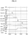
- FIG. 8 is a timing chart illustrating operation timing associated with reading a signal from a pixel in the pixel unit of the circuit diagram of FIG. 7 ;
- FIG. 9 is a timing chart illustrating operation timing associated with reading a signal from the test output amplifier of the test signal output unit in the circuit diagram of FIG. 7 ;
- FIG. 10 is a block diagram illustrating a solid-state image sensor according to a third embodiment, in which a circuit configuration of an output amplifier of the test signal output unit in FIG. 4 and a circuit configuration of a pixel in the pixel unit in FIG. 4 are illustrated;
- FIG. 11A is a timing chart illustrating operation timing associated with reading a signal from a pixel in the pixel unit of the circuit diagram of FIG. 10 ;
- FIG. 11B is a timing chart illustrating operation timing associated with reading a signal from the test output amplifier of the test signal output unit of the circuit diagram of FIG. 10 ;
- FIG. 12 is a block diagram illustrating a solid-state image sensor according to a first example, in which circuit configurations of a test signal generating unit that generates a test pattern in a column direction and a test signal output unit are illustrated;
- FIG. 13 is a diagram illustrating a solid-state image sensor according to a second example, in which circuit configurations of a test signal generating unit that generates a test pattern in a column direction and a test signal output unit are illustrated;
- FIG. 14 is a diagram illustrating a solid-state image sensor according to a third example, in which circuit configurations of a test signal generating unit that generates a test pattern in a column direction and a test signal output unit are illustrated;
- FIG. 15 is a schematic diagram illustrating an exemplary configuration of an imaging apparatus that uses the solid-state image sensor according to one of the embodiments.
- FIG. 1 is an illustration of variation in output signal levels in association with a white image on a black background.
- FIG. 2 is an illustration of variation in output signal levels in association with a black image on a white background.
- FIG. 3 is an illustration of an evaluation pattern for the variation in output signal levels in association with the white image on the black background illustrated in FIG. 1 .
- “Variation in output signal levels” in the solid-state image sensor is classified as a type of “horizontal stripe noise”.
- a stripe 5 that extends right to left from a white image 4 represents the variation in output signal levels, when there is the white image 4 in a black background 3 .
- a stripe 8 that extends right to left from a black image 7 represents the variation in output signal levels, when there is the black image 7 in a black background 6 .
- the variation in output signal levels as illustrated in FIG. 1 is, hereinafter, referred to as “variation of output signal level of white in a black background”
- the variation in output signal levels as illustrated in FIG. 2 is, hereinafter, referred to as “variation of output signal level of black in a white background” in the description to distinguish from each other.
- a method of quantitatively measuring the variation of output signal level of white in the black background includes calculating the difference in mean value between output of an area A, in which all pixels in the same row do not react to light but are fixed to a black level, and output of an area B, in which all pixels in the same row react to light.
- a method of quantitatively measuring the variation of the output signal level of black in the white background includes calculating the difference in mean value between output of an area A, in which all pixels in the same row react to light, and output of an area B, in which all pixels in the same row do not react to the light and are fixed to the black level.
- the solid-state image sensor is required to partially shield the surface of the solid-state image sensor from the light with a light shielding mask 9 to create these two areas, and needs an external operation to accomplish that goal. However, blocking out the light completely by external operation and reproducing an evaluation is difficult.
- FIG. 4 is a block diagram illustrating an exemplary configuration of a solid-state image sensor 10 having a parallel analog-to-digital (A/D) conversion element according to an embodiment of the present disclosure.
- the solid-state image sensor 10 of FIG. 4 includes a test signal generating unit 11 , a test signal output unit 12 , a pixel unit 13 , a read signal processing unit 14 , an output unit 15 , and a control circuit unit 16 .
- the pixel unit 13 includes a plurality of pixels, arranged in matrix, in each of which a signal that is photoelectrically converted from light into an electrical signal is amplified by an output amplifier to output a pixel signal.
- the read signal processing unit 14 reads out the pixel signal from the pixel unit 13 to a signal line in units of a single pixel or multiple pixels, and processes the pixel signal.
- the read signal processing unit 14 accordingly, includes an analog amplifier serving as a pixel reading circuit. Additionally, the read signal processing unit 14 may further include an analog-to-digital (A/D) conversion circuit.
- the output unit 15 includes an output amplifier used for an analog signal processed by the read signal processing unit 14 , and a differential amplification circuit for digital data used for a digital signal that is digitalized with the A/D conversion circuit.
- the test signal generating unit 11 requires no external operation for blocking out light in relation to variation in output signal levels, and includes a circuit to generate a test signal (voltage signal) for generating an evaluation pattern for quantitative evaluation, and the evaluation pattern can be reproduced.
- the evaluation pattern can measure the variation of output signal level of white in the black background and the variation of output signal level of black in the white background simultaneously, in a single shot.
- the test signal output unit 12 includes an output amplifier for testing (test output amplifier) for each signal line. Each test output amplifier is disposed in an area outside of the pixel unit 13 .
- the test signal output unit 12 outputs a signal from the test output amplifier to the signal line in response to input of the test signal to the test output amplifier.
- the test output amplifier inputs the test signal that is the evaluation pattern generated with the test signal generating unit 11 .
- a test evaluation pattern, which is artificially generated with the test signal generating unit 11 can be reproduced by the read signal processing unit 14 in the same way as the pixel of the pixel unit 13 is output.
- the test evaluation pattern artificially generated in the present embodiment, is a pattern that is generated by internal processing and is equal to the evaluation pattern generated by blocking out light externally.
- the control circuit unit 16 controls voltage generation and pulse drive conducted by the test signal generating unit 11 and timing to generate an internal clock to read the signals sequentially from the pixel unit 13 .
- the control circuit unit 16 also has a vertical scanning function to control a row address and row scanning, a signal processing control function of the read signal processing unit 14 , and an output control function of the output unit 15 .
- FIG. 5 is a block diagram illustrating a solid-state image sensor according to a first embodiment of the present disclosure, in which a detailed circuit configuration of an output amplifier (test output amplifier) of the test signal output unit 12 in FIG. 4 and a circuit configuration of a pixel of the pixel unit 13 in FIG. 4 are illustrated.
- the circuit configuration of FIG. 5 is described in terms of the pixels of the pixel unit 13 and the test output amplifier of the test signal output unit 12 .
- a pixel PX of the pixel unit 13 includes a photoelectric conversion element PD, a transfer transistor TX, a reset transistor RT, an amplifier transistor SF, and a floating diffusion node FD.
- the pixel PX includes a power supply VDD, a control line LTX of the transfer transistor TX, a control line LRT of the rest transistor RT, and a reset power supply control line LVDDRT.
- the amplifier transistor SF is configured as an output amplifier.
- the transfer transistor TX is connected between the photoelectric conversion element PD, such as a photo diode, and the floating diffusion node FD serving as an output node.
- the control circuit unit 16 applies a drive signal to the transfer control line LTX, the transfer transistor TX transfers electrons that are photoelectrically converted at the photoelectric conversion element PD to the floating diffusion node FD.
- the reset transistor RT is connected between the reset power supply control line LVDDRT and the floating diffusion node FD.
- a drive signal for resetting is applied to the gate of the reset transistor RT through the reset control line LRT, potential at the floating diffusion node FD is reset by the potential of the reset power supply control line LVDDRT.
- the floating diffusion node FD is connected to the gate of the amplifier transistor SF.
- the amplifier transistor SF is connected to a vertical signal line LVS and configured as a source follower circuit with a constant current source disposed outside the pixel unit 13 .
- the amplifier transistor SF amplifies the potential at the floating diffusion node FD and outputs a voltage corresponding to the potential to the vertical signal line LVS.
- the voltage output from each pixel PX is output to the read signal processing unit 14 , which is a signal reading circuit to read a signal from the pixel PX, through the vertical signal line LVS.
- the vertical signal line LVS used here, is a type of signal line.
- the pixel unit 13 actually includes a plurality pixels arranged in matrix.
- the reset control line LRT, the transfer control line LTX, and the reset power supply control line LVDDRT are wired as a set for each row.
- the control circuit unit 16 drives the reset control line LRT, the transfer control line LTX, and the reset power supply control line LVDDRT.
- the test signal output unit 12 includes an amplifier transistor for testing (test amplifier transistor) TSF, test signal input gate TFD, a power supply VDD, and the vertical signal line LVS.
- the read signal processing unit 14 includes an analog amplifier 14 a that processes a read signal and includes a column analog-to-digital (AD) convertor.
- AD analog-to-digital
- the test amplifier transistor TSF is connected between the power supply VDD and the vertical signal line LVS, and configured as a test output amplifier of a source follower circuit having a constant current source disposed outside the pixel unit 13 .
- the test amplifier transistor TSF amplifies potential at the test signal input gate TFD and outputs a voltage corresponding to the potential to the vertical signal line LVS.
- the test amplifier transistor TSF may have the same configuration and constant number as the amplifier transistor SF, which serves as an output amplifier of the pixel PX of the pixel unit 13 .
- the voltage output from the test signal generating unit 11 is input to the test signal input gate TFD as a test signal.
- FIG. 6A is a timing chart illustrating operation timing associated with reading a signal from a pixel PX of the pixel unit 13 in the circuit of FIG. 5 .
- FIG. 6B is a timing chart illustrating operation timing associated with reading a signal from the test output amplifier of the test signal output unit 12 in the circuit of FIG. 5 .
- a horizontal axis represents time in both FIG. 6A and FIG. 6B .
- a time tDark indicates a time of reading a reset signal from the pixel PX of the pixel unit 13 (hereinafter, referred to as a reset signal reading time tDark) and a time tSig indicates a time of reading a pixel signal level of the pixel PX (hereinafter, referred to as a pixel signal level reading time tSig).
- the control circuit unit 16 sets the reset power supply control line LVDDRT to the voltage of the power supply VDD, as illustrated in FIG. 6A , thereby activating pixel reading operation related to the pixel PX of the pixel unit 13 .
- the test signal generating unit 11 sets the test signal input gate TFD to ground (GND), thereby electrically disconnecting the test amplifier transistor TSF from the vertical signal line LVS in the test signal output unit 12 , so that the output signal of the pixel PX of the pixel unit 13 is read out.
- the control circuit unit 16 sets a reset voltage that flows through the reset control line LRT to a high (H) level voltage of power supply VDD before the reset signal reading time tDark. Through this, a reset operation of resetting the reset transistor RT to a reset voltage VFDdark of the floating diffusion node FD is performed.
- the amplifier transistor SF outputs the potential level VFDdark of the floating diffusion node FD reset by the reset voltage to the vertical signal line LVS, and then the potential level VFDdark is read out to the read signal processing unit 14 .
- the control circuit unit 16 sets the transfer transistor TX to the H level voltage of power supply VDD via the transfer control line LTX before the pixel signal level reading time tSig related to the pixel X, thereby charge-transferring electrons which are accumulated at the photoelectric conversion element PD to the floating diffusion node FD. Then, at the pixel signal level reading time tSig related to the pixel X, the amplifier transistor SF outputs to the vertical signal line LVS a voltage VFD that is a voltage of the signal level varied according to the number of charge-transferred electrons and a capacity of the floating diffusion node FD. That is, the pixel unit 13 reads out the signal to the read signal processing unit 14 .
- the control circuit unit 16 grounds the reset power supply control line LVDDRT and sets the reset control line LRT to power supply VDD. Through this, the floating diffusion node FD is also grounded, and an input level of the amplifier transistor SF of the pixel PX becomes a low (L) level, and thereby the amplifier transistor SF and the vertical signal line LVS are electrically disconnected.
- the test signal generating unit 11 generates a test signal of the voltage Vdark that is a voltage of the reset level of the floating diffusion node FD of the pixel PX (hereinafter, referred to as a reset level voltage Vdark, or simply a voltage Vdark) and a test signal of a voltage Vsig that is a voltage of the pixel signal level (hereinafter, referred to as a signal level voltage Vsig or simply a voltage Vsig).
- the test signals of the voltage Vdark and the voltage Vsig generated with the test signal generating unit 11 are input to the test signal input gate TFD.
- the test signal output unit 12 the output signal is read from the test amplifier transistor TSF to the vertical signal level LVS.
- the test amplifier transistor TSF of the test signal output unit 12 accordingly, becomes an output state to be tested.
- the test signal generating unit 11 inputs the potential level of the floating diffusion node FD that is the potential VFDdark to the test signal input gate TFD. Then, the signal, which is output to the vertical signal line LVS from the test amplifier transistor, is read out to the read signal processing unit 14 .
- the test signal generating unit 11 inputs the voltage VFDsig that is the signal level of the floating diffusion node FD to the test signal input gate TFD. Additionally, the transfer transistor TX is once boosted up to the H level voltage of power supply VDD with the transfer control line LTX. However, the reset power control line LVDDRT is at the ground level and the reset control line LRT is at the H level due to the voltage VDD so that the floating diffusion node FD is at the ground level. This allows the transfer control line LTX to operate in the same way as the reading operation of the pixel PX without charge-transferring the electrons accumulated at the photoelectric conversion element PD to the floating diffusion node FD.
- the test signal generating unit 11 inputs the voltage VFDsig that is a voltage of the signal level of the floating diffusion node FD to the test signal input gate TFD. Accordingly, the signal, which is output to the vertical signal line LVS from the test amplifier transistor TSF, is read out to the read signal processing unit 14 .
- the control circuit unit 16 operates the read signal processing unit 14 based on the output timing of the pixel signal in reading both the pixel signal and the test signal, respectively from the pixel unit 13 and the test signal output unit 12 .
- FIG. 7 is a block diagram illustrating a solid-state image sensor according to a second embodiment of the present disclosure, in which a circuit configuration of an output amplifier of a test signal output unit 12 in FIG. 4 and a circuit configuration of a pixel of a pixel unit 13 in FIG. 4 are illustrated.
- the pixel unit 13 includes a plurality of pixel groups. Circuit configurations of a pixel group of the pixel unit 13 and an output amplifier for testing (test output amplifier) of the test signal output unit 12 according to the second embodiment are individually described below.
- the pixel group of the pixel unit 13 includes a pixel 1 , a pixel 2 , a pixel output reset transistor SFR, a control line LSFR of the pixel output reset transistor SFR, and an amplifier transistor 2 SF.
- the pixel unit 13 of the second embodiment has a serial processing unit in each pixel group.
- the serial processing unit sequentially outputs pixel signals from pixels in the pixel group in time series.
- the pixel signals are read to a signal line on a pixel group basis.
- the pixel output reset transistor SFR is connected between ground and each of a pixel output OUT 1 of the pixel 1 , a pixel output OUT 2 of the pixel 2 , and an input gate of the amplifier transistor 2 SF.
- the amplifier transistor 2 SF is connected between a power supply VDD and a vertical signal line LVS.
- the pixel 1 includes a photoelectric conversion element PD 1 , a transfer transistor TX 1 , a reset transistor RT 1 , an amplifier transistor SF 1 , a selection transistor SW 1 , and a floating diffusion node FD 1 .
- the pixel 1 further includes a power supply VDD, a control line LTX 1 of the transfer transistor TX 1 , a control line LRT 1 and a reset power supply control line LVDDRT 1 of the reset transistor RT 1 , and a selection control line LSW 1 of the selection transistor SW 1 .
- the pixel 2 includes a photoelectric conversion element PD 2 , a transfer transistor TX 2 , a reset transistor RT 2 , an amplifier transistor SF 2 , a selection transistor SW 2 , and a floating diffusion node FD 2 .
- the pixel 2 further includes a power supply VDD, a control line LTX 2 of the transfer transistor TX 2 , a control line LRT 2 and a reset power supply control line LVDDRT 2 of the reset transistor RT 2 , and a selection control line LSW 2 of the selection transistor SW 2 .
- the transfer transistor TX 1 is connected between the photoelectric conversion element PD 1 , such as a photo diode, and the floating diffusion node FD 1 serving as an output node.
- the control circuit unit 16 applies a drive signal to the transfer control line LTX 1 , the transfer transistor TX 1 transfers electrons that are photoelectrically converted at the photoelectric conversion element PD 1 to the floating diffusion node FD 1 .
- the reset transistor RT 1 is connected between the reset power supply control line LVDDRT 1 and the floating diffusion node FD 1 .
- a drive signal for resetting is applied to the gate of the reset transistor RT 1 through the reset control line LRT 1 , potential at the floating diffusion node FD 1 is reset by potential of the reset power supply control line LVDDRT 1 .
- the floating diffusion node FD 1 is connected to the gate of the amplifier transistor SF 1 .
- the amplifier transistor SF 1 is connected to the pixel output OUT 1 via the selection transistor SW 1 and configured as a source follower circuit with a constant current source disposed outside the pixel unit 13 .
- the amplifier transistor SF 1 amplifies the potential at the floating diffusion node FD 1 and outputs a voltage corresponding to the potential to the pixel output OUT 1 .
- the pixel 2 has the same circuit configuration as the pixel 1 , and the amplifier transistor SF 2 amplifies potential at the floating diffusion node FD 2 and outputs a voltage corresponding to the potential to the pixel output OUT 2 .
- the amplifier transistor 2 SF is connected to the vertical signal line LVS and configured as a source follower circuit with a constant current source disposed outside the pixel unit 13 .
- the amplifier transistor 2 SF amplifies the potential of each of the pixel output OUT 1 and the pixel output OUT 2 , and serially outputs voltages corresponding to the potential to the vertical signal line LVS in time series, or performs serial output processing.
- the voltage output from each pixel group is output to the read signal processing unit 14 , which is a signal reading circuit that reads a pixel signal, through the vertical signal line LVS.
- the reset control line LRT 1 , the transfer control line LTX 1 , the reset power supply control line LVDDRT 1 , and the selection control line LSW 1 are wired as a set for each row.
- the reset control line LRT 2 , the transfer control line LTX 2 , the reset power supply control line LVDDRT 2 , and the selection control line LSW 2 are wired as a set for each row.
- the control circuit unit 16 drives the reset control lines LRT 1 and LRT 2 , the transfer control lines LTX 1 and LTX 2 , the reset power supply control lines LVDDRT 1 and LVDDRT 2 , and the selection control lines LSW 1 and LSW 2 .
- the test signal output unit 12 includes an amplifier transistor for testing (test amplifier transistor) T 2 SF, a test signal input gate T 2 OUT, a power supply VDD, and the vertical signal line LVS.
- the test amplifier transistor T 2 SF is connected between the power supply VDD and the vertical signal line LVS and configured as a source follower circuit with a constant current source disposed outside the pixel unit 13 .
- the test amplifier transistor TSF amplifies potential at the test signal input gate T 2 OUT and outputs a voltage corresponding to the potential to the vertical signal line LVS.
- the test amplifier transistor T 2 SF may have the same configuration and constant number as the amplifier transistor 2 SF, which serves as an output amplifier of the pixel group of the pixel unit 13 .
- the voltage output from the test signal generating unit 11 is input to the test signal input gate T 2 OUT as a test signal.
- FIG. 8 is a timing chart illustrating operation timing associated with reading a signal from a pixel in the pixel unit 13 of the circuit of FIG. 7 .
- FIG. 9 is a timing chart illustrating operation timing associated with reading a signal from the test output amplifier of the test signal output unit 12 in the circuit of FIG. 7 .
- operations of nodes which are shown in the circuit diagram of FIG. 7 , are individually illustrated and horizontal axis represents time.
- a time tDark 1 indicates a time of reading a reset signal from the pixel 1 of the pixel group of the pixel unit 13 (hereinafter, referred to as a reset signal reading time tDark 1 ) and a time tSig 1 indicates a time of reading a pixel signal level of the pixel 1 (hereinafter, referred to as a signal level reading time tSig 1 ).
- a reset signal reading time tDark 1 indicates a time of reading a reset signal from the pixel 1 of the pixel group of the pixel unit 13
- a time tSig 1 indicates a time of reading a pixel signal level of the pixel 1 (hereinafter, referred to as a signal level reading time tSig 1 ).
- a time tDark 2 indicates a time of reading a reset signal from the pixel 2 (hereinafter, referred to as a reset signal reading time tDark 2 ) and a time tSig 2 indicates a time of reading a pixel signal level of the pixel 2 (hereinafter, referred to as a signal level reading time tSig 2 ).
- the control circuit unit 16 sets the reset power supply control line LVDDRT 1 and the selection transistor SW 1 to the H level voltage of power supply VDD. This activates reading operation of the pixel 1 of the pixel group of the pixel unit 13 . Subsequently, the test signal generating unit 11 grounds the test signal input gate T 2 OUT, and thereby electrically disconnecting the test amplifier transistor T 2 SF from the vertical signal line LVS in the test signal output unit 12 , resulting in reading out of the signal from the pixel 1 of the pixel unit 13 .
- the control circuit unit 16 switches a connection of the selection control line LSW 1 of the selection transistor SW 1 from the power supply VDD to the ground and a connection of the selection control line LSW 2 of the selection transistor SW 2 from the ground to the power supply VDD, and thereby activating an reading operation to sequentially read pixels in the pixel group in time series.
- the reading operation of reading the output signal of the pixel 1 and the pixel 2 in the pixel group is described in time series below.
- the processing of reading the pixel 1 is described in time series with reference to FIG. 8 .
- the control circuit unit 16 sets the reset control line LRT 1 to the H level voltage of power supply VDD before the reset signal reading time tDark 1 .
- the reset transistor RT 1 accordingly, becomes a reset voltage Vout_dark that is a reset voltage of the floating diffusion node FD 1 due to the reset operation.
- the amplifier transistor SF 1 outputs the potential level Vout_dark of the floating diffusion node FD 1 reset with the reset voltage to the pixel output OUT 1 .
- the output of the pixel output OUT 1 is read out to the read signal processing unit 14 from the amplifier transistor 2 SF through the vertical signal line LVS, as an input signal.
- the control circuit unit 16 sets the transfer transistor TX 1 to the H level of the voltage VDD via the transfer control line LTX 1 before the pixel signal level reading time tSig 1 . Through this, electrons accumulated at the photoelectric conversion element PD 1 are charge-transferred to the floating diffusion node FD 1 .
- the amplifier transistor SF 1 outputs to the pixel output OUT 1 a voltage Vout_Sig 1 that is a voltage of the signal level varied according to the number of charge-transferred electrons and a capacity of the floating diffusion node FD 1 .
- the output of the pixel output OUT 1 is read out to the read signal processing unit 14 from the amplifier transistor 2 SF through the vertical signal line LVS, as an input signal.
- the control circuit unit 16 switches a control line, which controls reading operation, from the control line LRT 1 of the reset transistor RT 1 of the pixel 1 to the control line LRT 2 of the reset transistor RT 2 of the pixel 2 .
- the control circuit unit 16 also changes from the control line LTX 1 of the transfer transistor TX 1 to the control line TX 2 of the transfer transistor TX 2 .
- the potential Vout_dark of the pixel signal reset signal of the pixel 2 and the potential Vout_sig 2 of the pixel signal level of the pixel 2 are input to the amplifier transistor 2 SF in the pixel group. Through this, the amplifier transistor 2 SF outputs the pixel signal to the vertical signal line LVS.
- the control circuit unit 16 connects the control line LSW 1 of the selection transistor SW 1 of the pixel 1 and the control line LSW 2 of the selection transistor SW 2 of the pixel 2 to the ground, and sets the control line LSFR of the pixel output reset transistor SFR to the H level voltage of power supply VDD.
- the pixel outputs OUT 1 and OUT 2 are connected to the ground, accordingly. Through this, the input of the amplifier transistor 2 SF of the pixel group becomes the L level, and thus the amplifier transistor 2 SF and the vertical signal line LVS are electrically disconnected.
- the test signal generating unit 11 inputs test signals of the reset level voltage Vout_dark and the pixel signal level voltage Vout_sign to the test signal input gate T 2 OUT. Then, the test amplifier transistor T 2 SF of the test signal output unit 12 outputs the signal to the vertical signal level LVS. The test amplifier transistor T 2 SF of the test signal output unit 12 , accordingly, becomes an output state to be tested.
- the control circuit unit 16 Before the reset signal reading time tDark 1 , the control circuit unit 16 once boosts the reset control line LRT 1 up to the H level voltage with the power supply VDD at an operation timing of reading the pixel 1 of the pixel group. With this boost of the reset control line LRT 1 , the reset transistor RT 1 operates in the same way as the reset transistor RT 1 operates in the pixel signal reading operation.
- the test signal generating unit 11 inputs the potential Vout_dark, which is an output of the amplifier transistor SF 1 when the floating diffusion node FD 1 of the pixel 1 is the reset level, to the test signal input gate T 2 OUT. Then, the test amplifier transistor T 2 SF outputs the signal to the vertical signal line LVS, and the signal is read to the read signal processing unit 14 through the vertical signal line LVS.
- the test signal generating unit 11 inputs, to the test signal input gate T 2 OUT, the voltage Vout 1 _sig, which is a voltage output from the amplifier transistor SF 1 to which the pixel signal level of the floating diffusion node FD 1 is input.
- the control circuit unit 16 once boosts the transfer control line LTX 1 up to the H level voltage with the power supply VDD, and thus the transfer transistor TX 1 operates in the same way as the transfer transistor TX 1 operates in the pixel signal reading operation.
- the test signal generating unit 11 inputs, to the test signal input gate T 2 OUT, the potential Vout_sig, which is an output of the amplifier transistor SF 1 to which the pixels signal level of the floating diffusion node FD 1 is input. Then, the test amplifier transistor T 2 SF outputs the signal to the vertical signal line LVS, and the signal is read to the read signal processing unit 14 through the vertical signal line LVS.
- control circuit unit 16 switches a control line, which controls reading operation, from the control line LRT 1 of the reset transistor RT 1 of the pixel 1 to the control line LRT 2 of the reset transistor RT 2 of the pixel 2 .
- the control circuit unit 16 also changes from the control line LTX 1 of the transfer transistor TX 1 to the control line TX 2 of the transfer transistor TX 2 .
- the test signal generating unit 11 inputs, to the test signal input gate T 2 OUT, the potential Vout_dark that is an output of the amplifier transistor SF 2 when the floating diffusion node FD 2 of the pixel 2 is the reset level. Then, the test amplifier transistor T 2 SF outputs the signal to the vertical signal line LVS, and the signal is read to the read signal processing unit through the vertical signal line LVS.
- the test signal generating unit 11 inputs, to the test signal input gate T 2 OUT, the potential Vout_sig that is an output of the amplifier transistor SF 2 to which the pixel signal level of the floating diffusion node FD 2 is input. Then, the test amplifier transistor T 2 SF outputs the signal to the vertical signal line LVS, and the signal is read to the read signal processing unit 14 through the vertical signal line LVS.
- FIG. 10 is a block diagram illustrating a solid-state image sensor according to a third embodiment of the present disclosure, in which a circuit configuration of an output amplifier of a test signal output unit 12 in FIG. 4 and a circuit configuration of a pixel in the pixel unit 13 in FIG. 4 is illustrated.
- the pixel unit 13 includes a plurality of pixel groups. Circuit configurations of the pixel group of the pixel unit 13 and the test output amplifier of the test signal output unit 12 of FIG. 10 are individually described.
- a pixel group of a pixel unit 13 includes a pixel 1 , a pixel 2 , a pixel output reset transistor SFR, a control line LSFR of a pixel output reset transistor SFR, and an amplifier transistor 2 SF.
- the pixel output reset transistor SFR is connected between ground and each of a pixel output OUT 1 of the pixel 1 , a pixel output OUT 2 of the pixel 2 , and an input gate of the amplifier transistor 2 SF.
- the amplifier transistor 2 SF is connected between a power supply VDD and a vertical signal line LVS.
- the pixel 1 includes a photoelectric conversion element PD 1 , a transfer transistor TX 1 , a reset transistor RT 1 , an amplifier transistor SF 1 , a memory transfer transistor SL 1 , memory capacitor C 1 , a selection transistor SW 1 , and a floating diffusion node FD 1 .
- the pixel 1 further includes a power supply VDD, a control line LTX 1 of the transfer transistor TX 1 , a control line LRT 1 of the reset transistor RT 1 , and a reset power supply control line LVDDRT 1 of the reset transistor RT 1 .
- the pixel 1 also includes a memory selection control line LSL 1 of the memory transfer transistor SL 1 and a selection control line LSW 1 of the selection transistor SW 1 .
- the pixel 2 includes a photoelectric conversion element PD 2 , a transfer transistor TX 2 , a reset transistor RT 2 , an amplifier transistor SF 2 , a memory transfer transistor SL 2 , memory capacitor C 2 , a selection transistor SW 2 , and a floating diffusion node FD 2 .
- the pixel 2 further includes a power supply VDD, a control line LTX 2 of the transfer transistor TX 2 , a control line LRT 2 of the reset transistor RT 2 , and a reset power supply control line LVDDRT 2 of the reset transistor RT 2 .
- the pixel 2 also includes a memory selection control line LSL 2 of the memory transfer transistor SL 2 and a selection control line LSW 2 of the selection transistor SW 2 .
- the transfer transistor TX 1 is connected between the photoelectric conversion element PD 1 , such as a photo diode, and the floating diffusion node FD 1 serving as an output node.
- the control circuit unit 16 applies a drive signal to the transfer control line LTX 1 , the transfer transistor TX 1 transfers electrons that are photoelectrically converted at the photoelectric conversion element PD 1 to the floating diffusion node FD 1 .
- the reset transistor RT 1 is connected between the reset power supply control line LVDDRT 1 and the floating diffusion node FD 1 .
- a drive signal for resetting is applied to the gate of the reset transistor RT 1 through the reset control line LRT 1 , potential at the floating diffusion node FD 1 is reset by potential of the reset power supply control line LVDDRT 1 .
- the floating diffusion node FD 1 is connected to the gate of the amplifier transistor SF 1 .
- the amplifier transistor SF 1 is connected to the memory capacitor C 1 via the memory selection transistor SL 1 and configured as a source follower circuit with a constant current source disposed outside the pixel unit 13 .
- the amplifier transistor SF 1 amplifies the potential at the floating diffusion node FD 1 and stores a voltage corresponding to the potential in the memory capacitor C 1 .
- the selection transistor SW 1 is connected to the memory capacitor C 1 and the pixel output OUT 1 .
- the selection transistor SW 1 outputs the voltage stored in the memory capacitor C 1 to the pixel output OUT 1 .
- the pixel 2 has the same circuit configuration as the pixel 1 and outputs a voltage to the pixel output OUT 2 in the same way as pixel 1 .
- the amplifier transistor 2 SF is connected to the vertical signal line LVS and configured as an output amplifier of a source follower circuit having a constant current source disposed outside the pixel unit 13 .
- the amplifier transistor 2 SF amplifies the potential of each of the pixel output OUT 1 and the pixel output OUT 2 , and serially outputs voltages corresponding to the potential to the vertical signal line LVS in time series, or performs serial output processing.
- the voltage output from each pixel group is output to the read signal processing unit 14 , which is a signal reading circuit that reads a pixel signal, through the vertical signal line LVS.
- the reset control line LRT 1 In an array of pixel 1 of the pixel group of the pixel unit 13 , the reset control line LRT 1 , the transfer control line LTX 1 , the reset power supply control line LVDDRT 1 , and the selection control line LSW 1 are wired as a set for each row.
- the reset control line LRT 2 In an array of pixel 2 of the pixel group of the pixel unit 13 , the reset control line LRT 2 , the transfer control line LTX 2 , the reset power supply control line LVDDRT 2 , and the selection control line LSW 2 are wired as a set for each row.
- the control circuit unit 16 drives the reset control lines LRT 1 and LRT 2 , the transfer control lines LTX 1 and LTX 2 , the reset power supply control lines LVDDRT 1 and LVDDRT 2 , memory selection control lines LSL 1 and LSL 2 , and selection control lines LSW 1 and LSW 2 .
- the test signal output unit 12 includes an amplifier transistor for testing (test amplifier transistor) T 2 SF, a test signal input gate T 2 OUT, a power supply VDD, and the vertical signal line LVS.
- the test amplifier transistor T 2 SF is connected between the power supply VDD and the vertical signal line LVS and configured as a source follower circuit with a constant current source disposed outside the pixel unit 13 .
- the test amplifier transistor T 2 SF amplifies potential at the test signal input gate T 2 OUT and outputs a voltage corresponding to the potential to the vertical signal line LVS.
- the test amplifier transistor T 2 SF may have the same configuration and constant number as the amplifier transistor 2 SF, which serves as an output amplifier of the pixel group of the pixel unit 13 .
- the voltage output from the test signal generating unit 11 is input to the test signal input gate T 2 OUT as a test signal.
- FIG. 11A is a timing chart illustrating operation timing associated with reading a signal from a pixel in the pixel unit 13 in the circuit diagram of FIG. 10 .
- FIG. 11B is a timing chart illustrating operation timing associated with reading a signal from the test output amplifier of the test signal output unit 12 of the circuit diagram of FIG. 10 .
- FIG. 11A and FIG. 11B operations of nodes, which are shown in the circuit diagram of FIG. 10 , are individually illustrated and a horizontal axis represents time.
- a time tDark 1 indicates a time of reading a reset signal (hereinafter, referred to as a reset signal reading time tDark 1 ) from the pixel 1 of the pixel group of the pixel unit 13 and a time tSig 1 indicates a time of reading a pixel signal level of the pixel 1 (hereinafter, referred to as a signal level reading time tSig 1 ).
- a time tDark 1 indicates a time of reading a reset signal (hereinafter, referred to as a reset signal reading time tDark 1 ) from the pixel 1 of the pixel group of the pixel unit 13
- a time tSig 1 indicates a time of reading a pixel signal level of the pixel 1 (hereinafter, referred to as a signal level reading time tSig 1 ).
- a time tDark 2 indicates a time of reading a reset signal from the pixel 2 (hereinafter, referred to as a reset signal reading time tDark 2 ) and a time tSig 2 indicates a time of reading a pixel signal level of the pixel 2 (hereinafter, referred to as a signal level reading time tSig 2 ).
- the control circuit unit 16 sets the reset power supply control line LVDDRT and the selection control line LSW 1 of the selection transistor SW 1 to the H level voltage of power supply VDD, and thereby activating the pixel reading operation related to the pixel 1 of the pixel group of the pixel unit 13 .
- the test signal generating unit 11 grounds the test signal input gate T 2 OUT, and thereby electrically disconnecting the test amplifier transistor T 2 SF from the vertical signal line LVS in the test signal output unit 12 , and thus the output signal from the pixel 1 of the pixel unit 13 is read out.
- the control circuit unit 16 After controlling reading of pixel signal of the pixel 1 , the control circuit unit 16 switches a connection of the selection control line LSW 1 of the selection transistor SW 1 from the power supply VDD to the ground, and then a connection of the selection control line LSW 2 of the selection transistor SW 2 from the ground to the power supply VDD. This activates operation of reading from the pixels in the pixel group serially in time series.
- the control circuit unit 16 resets the potential at the floating diffusion nodes FD 1 and FD 2 before the reset signal reading time tDark 1 .
- the control circuit unit 16 sets each of the reset control lines LRT 1 and LRT 2 and each of the memory selection control lines LSL 1 and LSL 2 to H level voltage of power supply VDD, and thereby resetting the reset transistors RT 1 , RT 2 , and the memory selection transistors SL 1 and SL 2 .
- each output voltage corresponding to the reset level output from the amplifier transistors SF 1 and SF 2 is transferred to the corresponding one of the memory capacitor C 1 and the memory capacitor C 2 so that each memory can be reset.
- control circuit unit 16 connects the reset control line LRT 1 of the reset transistor RT 1 and the reset control line LRT 2 of the reset transistor RT 2 to the ground, which is the L level.
- the control circuit unit 16 then also connects the memory selection control line LSL 1 of the memory selection transistor SL 1 and the memory selection control line LSL 2 of the memory selection transistor SL 2 to the ground that is the L level.
- each output reset level voltage Vout_dark from the corresponding one of the amplifier transistors SF 1 and SF 2 is stored in the memory capacitor C 1 and the memory capacitor C 2 , respectively.
- the control circuit unit 16 boosts the control line LSW 1 of the selection transistor SW 1 up to the H level voltage of power supply VDD.
- the control circuit unit 16 connects the control line LSW 1 of the selection transistor SW 1 to the ground that is the L level, and boosts the control line LSW 2 of the selection transistor SW up to the H level voltage of power supply VDD.
- the pixel output OUT 2 of the pixel 2 is read and a signal is output from the amplifier transistor 2 SF to the read signal processing unit 14 through the vertical signal line LVS.
- the control circuit unit 16 sets the transfer control line LTX 1 of the transfer transistor TX 1 and the transfer control line LTX 2 of the transfer transistor TX 2 to the H level voltage with the power supply VDD.
- the control circuit unit 16 also sets the memory selection control line LSL 1 of the memory selection transistor SL 1 and the memory selection control line LSL 2 of the memory selection transistor SL 2 to the H level voltage with the power supply VDD.
- electrons are charge-transferred from the photoelectric conversion elements PD 1 and PD 2 to the floating diffusion nodes FD 1 to FD 2 , respectively.
- Each output voltage corresponding to each signal level from the amplifier transistors SF 1 and SF 2 is transferred to and stored in the corresponding one of the memory capacitor C 1 and the memory capacitor C 2 .
- the pixel signal from each pixel in the pixel group is stored in the memory capacitor in each pixel as described above.
- control circuit unit 16 connects the transfer control line LTX 1 of the transfer transistor TX 1 and the transfer control line LTX 2 of the transfer transistor TX 2 to the ground that is the L level.
- the control circuit unit 16 then connects the memory selection control line LSL 1 of the memory selection transistor SL 1 and the memory selection control line LSL 2 of the memory selection transistor SL 2 to the ground that is the L level.
- the output voltage Vout_sig of the signal level of the amplifier transistors SF 1 and SF 2 is stored in the memory capacitor C 1 and the memory capacitor C 2 .
- the control circuit unit 16 boosts the control line LSW 1 of the selection transistor SW 1 up to the H level voltage of power supply VDD at the pixel signal level reading time t Sig 1 .
- the control circuit unit 16 connects the control line LSW 1 of the selection transistor SW 1 to the ground of L level, and boosts the control line LSW 2 of the selection transistor SW 2 up to the power supply VDD of H level. Through this, an output signal of the pixel output OUT 2 of the pixel 2 is read from the amplifier transistor 2 SF to the read signal processing unit 14 through the vertical signal line LVS.
- the control circuit unit 16 connects the selection control line LSW 1 of the selection transistor SW 1 of the pixel 1 and the selection control line LSW 2 of the selection transistor SW 2 to the ground, and sets the control line LSFR of the pixel output reset transistor SFR to the H level voltage of power supply VDD, and thereby connecting the pixel outputs OUT 1 and OUT 2 to the ground.
- the input of the amplifier transistor 2 SF of the pixel group becomes the L level and the amplifier transistor 2 SF and the vertical signal line LVS are electrically disconnected.
- the test signal generating unit 11 generates a test signal of the reset level voltage Vout_dark that is a voltage of the reset level of each of the pixel outputs OUT 1 and the OUT 2 and a test signal of a voltage Vsig that is a voltage of the pixel signal level.
- the test signal voltages V_dark and the voltage V_sig are input to the test signal input gate T 2 OUT.
- the test amplifier transistor T 2 SF of the test signal output unit 12 outputs the signal to the vertical signal level LVS. Through this, the test amplifier transistor T 2 SF of the test signal output unit 12 enters in an output state to be tested.
- test signal generating unit 11 The operation of inputting the signal generated with the test signal generating unit 11 to the test signal input gate T 2 OUT of the test signal outputting unit 12 and reading the signal from the test amplifier transistor T 2 SF of the test signal output unit 12 is described in time series below. Before the reset signal reading time tDark 1 , the test signal generating unit 11 generates and inputs the pixel output reset level Vout_dark to the input gate T 2 OUT of the test signal input gate of the test signal output unit 12 .
- the control circuit unit 16 sets the reset control line LRT 1 of the reset transistor and the reset control line LRT 2 of the reset transistor RT 2 to the H level voltage of power supply VDD in the same way as the reading operation of the output signal.
- the control circuit unit 16 also sets the memory selection control line LSL 1 of the memory selection transistor SL 1 and the memory selection control line LSL 2 of the memory selection transistor SL 2 to the H level voltage of power supply VDD.
- the pixel unit 13 resets the potential of the floating diffusion nodes FD 1 and FD 2 to the reset potential.
- each output voltage corresponding to the reset level of the corresponding one of the amplifier transistors SF 1 and SF 2 is transferred to the corresponding one of the memory capacitor C 1 and the memory capacitor C 2 so that each memory is reset.
- the control circuit unit 16 then connects the reset control line LRT 1 of the reset transistor RT 1 and the reset control line LRT 2 of the reset transistor RT 2 to the ground that is the L level.
- the control circuit unit 16 then connects the memory selection control line LSL 1 of the memory selection transistor SL 1 and the memory selection control line LSL 2 of the memory selection transistor SL 2 to the ground that is the L level.
- the output voltage Vout_dark from each of the amplifier transistors SF 1 and SF 2 is stored in the corresponding one of the memory capacitor C 1 and the memory capacitor C 2 .
- the test signal generating unit 11 At the reset signal reading time tDark 1 and the reset signal reading time tDark 2 , the test signal generating unit 11 generates and inputs the output voltage Vout_dark to the test signal input gate 2 OUT of the test signal output unit 12 . Then, the test amplifier transistor T 2 SF outputs the signal to the vertical signal line LVS, and the signal is read to the read signal processing unit through the vertical signal line LVS.
- the pixel output level voltage Vout_sig generated with the test signal generating unit 11 is input to the test signal input gate T 2 OUT of the test signal output unit 12 .
- the control circuit unit 16 sets the transfer control line LTX 1 of the transfer transistor TX 1 the transfer control line LTX 2 of the transfer transistor TX 2 to the H level voltage of power supply VDD.
- the control circuit unit 16 also sets the memory selection control line LSL 1 of the memory selection transistor SL 1 and the memory selection control line LSL 2 of the memory selection transistor SL 2 to the H level voltage of power supply VDD.
- electrons are charge-transferred from the photoelectric conversion elements PD 1 and PD 2 to each of the floating diffusion nodes FD 1 and FD 2 .
- the output voltage corresponding to the signal level of each of the amplifier transistors SF 1 and SF 2 is stored in the corresponding one of the memory capacitors C 1 and C 2 .
- control circuit unit 16 connects the transfer control line LTX 1 of the transfer transistor TX 1 and the transfer control line LTX 2 of the transfer transistor TX 2 to the ground that is the L level.
- the control circuit unit 16 then also connects the memory selection control line LSL 1 of the memory selection transistor SL 1 and the memory selection control line LSL 2 of the memory selection transistor SL 2 to the ground that is the L level.
- the output voltage Vout_sig of the signal level of each of the amplifier transistors SF 1 and SF 2 is stored in the corresponding one of the memory capacitor C 1 and the memory capacitor C 2 .
- the pixel output level voltage Vout_sig generated with the test signal generating unit 11 is input to the test signal input gate T 2 OUT of the test signal output unit 12 .
- the test amplifier transistor T 2 SF outputs the signal to the vertical signal line LVS, and the signal is read to the read signal processing unit through the vertical signal line LVS.
- FIG. 12 is a block diagram illustrating circuit configurations of the test signal generating unit 11 and the test signal output unit 12 , according to a first example in the case of generating a test pattern in a column direction.
- the control circuit unit 16 in addition to the example configurations of the test signal generating unit 11 and the test signal output unit 12 for evaluating variation of output signal level of white in a black background, the control circuit unit 16 , the pixel unit 13 , and the read signal processing unit 14 are illustrated.
- the control circuit unit 16 , the pixel unit 13 , and the read signal processing unit 14 each has the same circuit configuration as the corresponding components illustrated in FIG. 5 .
- a vertical signal line LVS for one of a set of successive columns from 1 to k and a set of successive columns from m+1 to n is defined as a light shielding group (or light shielding part), and the vertical signal lines LVS for a set of successive columns from k+1 to m is defined as a non-light shielding group (or non-light shielding part).
- k, m, and n are integer numbers, and n>m>k>0. Accordingly, in this description, successive signal lines are the light shielding group and one or more signal lines other than the successive signal lines of the light shielding group are the non-light shielding group.
- the test signal generating unit 11 inputs a light shielding pulse to the test signal input gate TFD of the test amplifier transistor TSF that is connected to the vertical signal line LVS of the light shielding groups, which are the columns from 1 to k and the columns from m+1 to n in the test signal output unit 12 .
- the test signal generating unit 11 inputs a non-light shielding pulse to the test signal input gate TFD of the test amplifier transistor TSF connected to the vertical signal line LVS of the non-light shielding group, which is the columns from k+1 to m.
- the light shielding pulse and the non-light shielding pulse are synchronized with the time tDark at which a reset level signal output form a pixel of the pixel unit 13 is read, and the pixel signal level reading time tSig.
- the reset level voltage Vdark is usually applied
- the non-light shielding pulse the reset level voltage Vdark is applied at the time tDark and then lowered to the voltage Vsig right before the time tSig.
- the voltage Vdark and the voltage Vsig are generated based on a reference voltage Vre that is provided to the test signal generating unit 11 from the inside or the outside.
- FIG. 13 is a block diagram illustrating circuit configurations of the test signal generating unit 11 and the test signal output unit 12 , according to a second example in the case of generating a test pattern in a column direction.
- the test signal generating unit 11 provides the voltages Vdark and Vsig to the test signal output unit 12 .
- the test signal generating unit 11 includes input voltage switches SWV each of which is arranged corresponding to the test signal input gate TFD of the test amplifier transistor TSF corresponding to each vertical signal line LVS of the test signal output unit 12 .
- the input voltage switch SWV switches an input voltage according to one of the light shielding signal pulse and the non-light shielding signal pulse.
- Each input voltage switch SWV is controlled by the control circuit unit 16 using the light shielding signal pulse or the non-light shielding signal pulse.
- the input voltage switch SWV switches the input voltage in a manner that the potential of the reset level voltage Vdark generated with the test signal generating unit 11 is applied to the test signal input gate TFD of the test amplifier transistor TSF.
- the input voltage switch SWV switches the input voltage in a manner that the potential of the signal level voltage Vsig generated with the test signal generating unit 11 is applied to the test signal input gate TFD of the test amplifier transistor TSF.
- the voltage Vdark is input to the test signal input gate TFD of each test amplifier transistor TSF corresponding to the vertical signal line LVS of one of the light shielding groups each of which is the columns from 1 to k or the columns from m+1 to n, because a signal of H level is normally input to the input voltage switch SWV due to the light shielding pulse. Additionally, the voltage Vdark is input to the test signal input gate TFD of the test amplifier transistor TSF corresponding to the vertical signal line LVS of the non-light shielding group of the columns from k+1 to m because, a signal of H level is normally input to the input voltage switch SWV due to the non-light shielding pulse. At the time tSig, the signal of L level is input, and the voltage Vsig is input, accordingly.
- FIG. 14 is a diagram illustrating circuit configurations of the test signal generating unit 11 and the test signal output unit 12 , according to a third example in the case of generating a test pattern in a column direction.
- the test signal generating unit 11 provides the light shielding pulse or the non-light shielding pulse of one of the voltage Vdark or the voltage Vsig to the test signal output unit 12 .
- the test signal generating unit 11 includes pulse switches SWP each of which is arranged corresponding to the test signal input gate TFD of the test amplifier transistor TSF corresponding to each vertical signal line LVS of the test signal output unit 12 .
- the pulse switch SWP switches an input pulse according to one of a light shielding signal and a non-light shielding signal.
- Each pulse switch SWP is controlled by the control circuit unit 16 using the light shielding signal or the non-light shielding signal.
- the pulse switch SWP switches in a manner that the light shielding pulse generated with the test signal generating unit 11 is applied to the test signal input gate TFD of the test amplifier transistor TSF.
- the pulse switch SWP switches in a manner that the non-light shielding pulse generated with the test signal generating unit 11 is applied to the test signal input gate TFD of the test amplifier transistor TSF.
- a light shielding signal of H level is normally applied to the pulse switch SWP corresponding to the test signal input gate TFD of the test amplifier transistor TSF corresponding to the vertical signal line LVS of one of the light shielding groups each of which is the columns from 1 to k or the columns from m+1 to n, and thereby the light shielding pulse is input to the test signal input gate TFD.
- the light shielding pulse is normally the voltage Vdark.
- a light shielding signal of L level is normally applied to the pulse switch SWP corresponding to the test signal input gate TFD of the test amplifier transistor TSF corresponding to the vertical signal lines LVS of the light shielding group of the columns from k+1 to m, and thereby the non-light shielding pulse is input to the test signal input gate TFD.
- the voltage Vdark is input to the test signal input gate TFD at the time tDark
- the voltage Vsig is input to the test signal input gate TFD at the time tSig.
- the solid-state image sensor in one of the embodiments described above can perform a quantitative evaluation for a parallel processing operation for pixel signal reading from the signal lines of output of the amplifier transistors SF of pixels of the pixel unit 13 to the read signal processing unit 14 using an evaluation pattern.
- a test signal is directly input to a read signal processing unit including an A/D converter circuit, however, in this embodiments, a signal can be input to the signal line of the pixel via the test output amplifier, so that a impedance state from the signal line to the read signal processing unit can also be evaluated. Additionally, generating the same output state as an actual pixel is possible by inputting the test signal to the same output amplifier as the output amplifier of a pixel of the pixel unit.
- solid-state image sensor of any one of the above-described embodiments may be configured as described below.
- a serial processing unit of a pixel group of a pixel unit 13 may be disconnected from a signal line by connecting an input to ground.
- a test output amplifier of a test signal output unit 12 may have the same configuration and constant number as an output amplifier of each pixel of the pixel unit 13 .
- the test output amplifier of the test signal output unit 12 may have the same configuration as the serial processing unit of the pixel group of the pixel unit 13 .
- a control circuit unit 16 may perform the control operation as described follows: In reading a pixel signal from the pixel unit 13 , the test signal output unit 12 connects the output amplifier to the signal line by setting an input of the output amplifier of the test signal output unit 12 to the L level, resulting in output of the pixel signal from the pixel unit 13 to the signal line. In reading the test signal of the test signal output unit 12 , the output of a pixel signal of the output amplifier of each pixel of the pixel unit 13 or the serial processing unit is disconnected from the signal line by setting an input signal of the output amplifier of each pixel of the pixel unit 13 or the serial processing unit to the L level. This allows the output amplifier of the test signal output unit 12 to output the test signal to the signal line.
- a test signal generating unit 11 preferably has a reference voltage to generate a plurality of voltages.
- the control circuit unit 16 causes the test signal generating unit 11 to transit a voltage of the output amplifier of the pixel or the input of the serial processing unit from a pixel reset level to a signal level by synchronizing with a pixel signal reading time.
- Amplitude of the voltage generated at the test signal generating unit 11 is preferably larger than an input range of the output amplifier of the pixel or the serial processing unit.
- the test signal generating unit 11 desirably changes the amplitude of the voltage output to the test output amplifier of the test signal output unit 12 for each column or each line.
- the pixel unit 13 may be divided into two parts, a left pixel part and a right pixel part, and the test signal generating unit 11 may be divided into a first test signal generating unit for the left pixel part and a second test signal generating unit for the right pixel part.
- the solid-state imaging device accordingly, may include more than two test signal generating units and be able to control each test signal generating unit independently.
- FIG. 15 is a schematic diagram illustrating an exemplary configuration of an imaging apparatus that uses the solid-state image sensor of the disclosure.
- An imaging apparatus 20 includes an imaging device 21 with the solid-state image sensor 10 .
- the imaging apparatus includes, for example, a camera system.
- the solid-state image sensor 10 may be any one of the embodiments described above.
- the imaging apparatus 20 includes a lens 22 configured as an optical system that form an object image on an imaging surface of the solid-state image sensor 10 of the imaging device 21 using incident light.
- the imaging apparatus 20 further includes a driving device 23 to drive the imaging device 21 and a signal processing device 24 to process an output signal of the imaging device 21 .
- the driving device 23 includes a timing generator (drive-timing signal generating circuit) to drive circuits in the imaging device 21 including the solid-state image sensor 10 , and drives the imaging device 21 with a predetermined timing signal.
- the signal processing device 24 processes an output signal of the imaging device 21 .
- an image signal processed with the signal processing device 24 is stored in a recording medium, such as a memory, via an analog signal processing unit (AFE). Image information recorded to the recording medium is copied as a hard copy using, for example, a printer.
- the image signal processed with the signal processing device 24 may be displayed as a moving image on a monitor such as a liquid crystal display.
- Implementing the solid-state image sensor 10 of the disclosure to the imaging device 21 can embody an imaging apparatus with a high accuracy, such as a camera system. Imaging device 21 may also be used in other imaging apparatuses than a camera system.
Landscapes
- Engineering & Computer Science (AREA)
- Multimedia (AREA)
- Signal Processing (AREA)
- Health & Medical Sciences (AREA)
- Biomedical Technology (AREA)
- General Health & Medical Sciences (AREA)
- Solid State Image Pick-Up Elements (AREA)
- Transforming Light Signals Into Electric Signals (AREA)
Abstract
Description
Claims (12)
Applications Claiming Priority (2)
| Application Number | Priority Date | Filing Date | Title |
|---|---|---|---|
| JP2016056326A JP6733245B2 (en) | 2016-03-18 | 2016-03-18 | Solid-state imaging device and imaging device |
| JP2016-056326 | 2016-03-18 |
Publications (2)
| Publication Number | Publication Date |
|---|---|
| US20170272742A1 US20170272742A1 (en) | 2017-09-21 |
| US10630968B2 true US10630968B2 (en) | 2020-04-21 |
Family
ID=59847232
Family Applications (1)
| Application Number | Title | Priority Date | Filing Date |
|---|---|---|---|
| US15/450,480 Expired - Fee Related US10630968B2 (en) | 2016-03-18 | 2017-03-06 | Solid-state image sensor and imaging apparatus |
Country Status (2)
| Country | Link |
|---|---|
| US (1) | US10630968B2 (en) |
| JP (1) | JP6733245B2 (en) |
Cited By (1)
| Publication number | Priority date | Publication date | Assignee | Title |
|---|---|---|---|---|
| US11516423B2 (en) | 2020-03-18 | 2022-11-29 | Ricoh Company, Ltd. | Photoelectric conversion device and image forming apparatus |
Families Citing this family (6)
| Publication number | Priority date | Publication date | Assignee | Title |
|---|---|---|---|---|
| JP6769349B2 (en) | 2017-03-03 | 2020-10-14 | 株式会社リコー | Solid-state image sensor and image sensor |
| JP6969224B2 (en) | 2017-08-24 | 2021-11-24 | 株式会社リコー | Solid-state image sensor and image sensor |
| JP6889639B2 (en) | 2017-09-12 | 2021-06-18 | 株式会社ダイセル | Plastic lens |
| JP7159568B2 (en) | 2018-02-23 | 2022-10-25 | 株式会社リコー | Photoelectric conversion device, image reading device, and image forming device |
| JP7322552B2 (en) | 2019-07-01 | 2023-08-08 | 株式会社リコー | Photoelectric conversion device, line sensor, image reading device, and image forming device |
| JP7298373B2 (en) | 2019-07-31 | 2023-06-27 | 株式会社リコー | Photoelectric conversion device, image reading device, and image forming device |
Citations (9)
| Publication number | Priority date | Publication date | Assignee | Title |
|---|---|---|---|---|
| JP2000324404A (en) | 1999-05-14 | 2000-11-24 | Toshiba Corp | Solid-state image pickup unit |
| US20080259164A1 (en) * | 2007-04-18 | 2008-10-23 | Sony Corporation | Data transfer circuit, solid-state imaging device, and camera system |
| JP2010114487A (en) | 2008-11-04 | 2010-05-20 | Sony Corp | Solid-state image pickup apparatus and image pickup apparatus |
| US20110279724A1 (en) * | 2010-05-13 | 2011-11-17 | Sony Corporation | Solid-state imaging device and camera system |
| JP2012039299A (en) | 2010-08-05 | 2012-02-23 | Toshiba Corp | Solid state imaging device |
| US20120194716A1 (en) * | 2011-01-31 | 2012-08-02 | Olympus Corporation | Image pickup device |
| US20120228609A1 (en) | 2011-03-09 | 2012-09-13 | Canon Kabushiki Kaisha | Test circuit for testing signal receiving unit, image pickup apparatus, method of testing signal receiving unit, and method of testing image pickup apparatus |
| JP2015106908A (en) | 2013-12-03 | 2015-06-08 | 株式会社リコー | Column readout circuit and solid-state imaging apparatus |
| US20160006961A1 (en) * | 2014-07-04 | 2016-01-07 | Naoki ASABA | Photoelectric conversion element, image reading device, image forming apparatus, and signal control method |
-
2016
- 2016-03-18 JP JP2016056326A patent/JP6733245B2/en not_active Expired - Fee Related
-
2017
- 2017-03-06 US US15/450,480 patent/US10630968B2/en not_active Expired - Fee Related
Patent Citations (11)
| Publication number | Priority date | Publication date | Assignee | Title |
|---|---|---|---|---|
| JP2000324404A (en) | 1999-05-14 | 2000-11-24 | Toshiba Corp | Solid-state image pickup unit |
| US20080259164A1 (en) * | 2007-04-18 | 2008-10-23 | Sony Corporation | Data transfer circuit, solid-state imaging device, and camera system |
| JP2010114487A (en) | 2008-11-04 | 2010-05-20 | Sony Corp | Solid-state image pickup apparatus and image pickup apparatus |
| US20110279724A1 (en) * | 2010-05-13 | 2011-11-17 | Sony Corporation | Solid-state imaging device and camera system |
| JP2011239344A (en) | 2010-05-13 | 2011-11-24 | Sony Corp | Solid-state imaging device and camera system |
| JP2012039299A (en) | 2010-08-05 | 2012-02-23 | Toshiba Corp | Solid state imaging device |
| US20120194716A1 (en) * | 2011-01-31 | 2012-08-02 | Olympus Corporation | Image pickup device |
| US20120228609A1 (en) | 2011-03-09 | 2012-09-13 | Canon Kabushiki Kaisha | Test circuit for testing signal receiving unit, image pickup apparatus, method of testing signal receiving unit, and method of testing image pickup apparatus |
| JP2012199913A (en) | 2011-03-09 | 2012-10-18 | Canon Inc | Signal reception section test circuit, imaging apparatus, signal reception section test method and test method of imaging apparatus |
| JP2015106908A (en) | 2013-12-03 | 2015-06-08 | 株式会社リコー | Column readout circuit and solid-state imaging apparatus |
| US20160006961A1 (en) * | 2014-07-04 | 2016-01-07 | Naoki ASABA | Photoelectric conversion element, image reading device, image forming apparatus, and signal control method |
Non-Patent Citations (1)
| Title |
|---|
| Office Action dated Dec. 10, 2019, issued in corresponding Japanese Patent Application No. 2016-056326, six pages. |
Cited By (1)
| Publication number | Priority date | Publication date | Assignee | Title |
|---|---|---|---|---|
| US11516423B2 (en) | 2020-03-18 | 2022-11-29 | Ricoh Company, Ltd. | Photoelectric conversion device and image forming apparatus |
Also Published As
| Publication number | Publication date |
|---|---|
| JP6733245B2 (en) | 2020-07-29 |
| US20170272742A1 (en) | 2017-09-21 |
| JP2017175239A (en) | 2017-09-28 |
Similar Documents
| Publication | Publication Date | Title |
|---|---|---|
| US10630968B2 (en) | Solid-state image sensor and imaging apparatus | |
| US8289431B2 (en) | Image sensing device and image sensing system | |
| CN107683603B (en) | Solid-state imaging element, electronic device, and control method of solid-state imaging element | |
| US7755686B2 (en) | Physical quantity distribution detecting apparatus and imaging apparatus | |
| KR101711702B1 (en) | Imaging apparatus, imaging system, and method for driving imaging apparatus | |
| US7622699B2 (en) | Solid-state image pickup device, a method of driving the same, a signal processing method for the same, and image pickup apparatus | |
| US7961237B2 (en) | Photoelectric conversion device and image sensing system | |
| US9979913B2 (en) | Driving method of imaging device and driving method of imaging system | |
| US20090273695A1 (en) | Solid-state image pickup apparatus, drive method for the solid-state image pickup apparatus, and image pickup apparatus | |
| CN101990070A (en) | Solid-state image sensing device, analog-digital conversion method of solid-state image sensing device, and electronic apparatus | |
| US9961282B2 (en) | Image pickup apparatus and image pickup system | |
| US20170155856A1 (en) | Driving method for an image pickup apparatus, image pickup apparatus, and image pickup system | |
| US9426391B2 (en) | Solid-state imaging apparatus, method of controlling the same, and imaging system | |
| JP2010283735A (en) | Detection device and solid-state imaging device | |
| JP2020167542A (en) | Imaging equipment and signal processing equipment | |
| US8553121B2 (en) | Imaging apparatus and control method thereof | |
| CN104935834A (en) | solid state imaging device | |
| JP2008017011A (en) | Solid imaging apparatus | |
| US12238443B2 (en) | Photoelectric conversion device and imaging system | |
| JPH03225868A (en) | Solid-state image pickup element and image pickup device using same | |
| KR20150140385A (en) | Solid-state image capture element and image capture device | |
| JP2022071983A (en) | Ramp signal output circuit, photoelectric conversion apparatus, and capturing system | |
| US10397501B2 (en) | Solid-state image sensor and imaging apparatus | |
| JP7257299B2 (en) | Imaging system and imaging system application equipment | |
| US20160323529A1 (en) | Signal readout circuit, imaging apparatus, and imaging system |
Legal Events
| Date | Code | Title | Description |
|---|---|---|---|
| AS | Assignment |
Owner name: RICOH COMPANY, LTD., JAPAN Free format text: ASSIGNMENT OF ASSIGNORS INTEREST;ASSIGNORS:SUZUKI, ATSUSHI;KANNO, TOHRU;MIYOSHI, YUUYA;REEL/FRAME:041475/0763 Effective date: 20170302 |
|
| STPP | Information on status: patent application and granting procedure in general |
Free format text: NON FINAL ACTION MAILED |
|
| STPP | Information on status: patent application and granting procedure in general |
Free format text: RESPONSE TO NON-FINAL OFFICE ACTION ENTERED AND FORWARDED TO EXAMINER |
|
| FEPP | Fee payment procedure |
Free format text: PETITION RELATED TO MAINTENANCE FEES GRANTED (ORIGINAL EVENT CODE: PTGR); ENTITY STATUS OF PATENT OWNER: LARGE ENTITY |
|
| STPP | Information on status: patent application and granting procedure in general |
Free format text: NOTICE OF ALLOWANCE MAILED -- APPLICATION RECEIVED IN OFFICE OF PUBLICATIONS |
|
| STPP | Information on status: patent application and granting procedure in general |
Free format text: AWAITING TC RESP., ISSUE FEE NOT PAID |
|
| STPP | Information on status: patent application and granting procedure in general |
Free format text: PUBLICATIONS -- ISSUE FEE PAYMENT RECEIVED |
|
| STCF | Information on status: patent grant |
Free format text: PATENTED CASE |
|
| FEPP | Fee payment procedure |
Free format text: MAINTENANCE FEE REMINDER MAILED (ORIGINAL EVENT CODE: REM.); ENTITY STATUS OF PATENT OWNER: LARGE ENTITY |
|
| LAPS | Lapse for failure to pay maintenance fees |
Free format text: PATENT EXPIRED FOR FAILURE TO PAY MAINTENANCE FEES (ORIGINAL EVENT CODE: EXP.); ENTITY STATUS OF PATENT OWNER: LARGE ENTITY |
|
| STCH | Information on status: patent discontinuation |
Free format text: PATENT EXPIRED DUE TO NONPAYMENT OF MAINTENANCE FEES UNDER 37 CFR 1.362 |
|
| FP | Lapsed due to failure to pay maintenance fee |
Effective date: 20240421 |