US10629589B2 - Resistor fins - Google Patents
Resistor fins Download PDFInfo
- Publication number
- US10629589B2 US10629589B2 US15/991,143 US201815991143A US10629589B2 US 10629589 B2 US10629589 B2 US 10629589B2 US 201815991143 A US201815991143 A US 201815991143A US 10629589 B2 US10629589 B2 US 10629589B2
- Authority
- US
- United States
- Prior art keywords
- resistor
- fins
- nitride
- substrate
- present
- Prior art date
- Legal status (The legal status is an assumption and is not a legal conclusion. Google has not performed a legal analysis and makes no representation as to the accuracy of the status listed.)
- Expired - Fee Related
Links
Images


Classifications
-
- H—ELECTRICITY
- H10—SEMICONDUCTOR DEVICES; ELECTRIC SOLID-STATE DEVICES NOT OTHERWISE PROVIDED FOR
- H10D—INORGANIC ELECTRIC SEMICONDUCTOR DEVICES
- H10D84/00—Integrated devices formed in or on semiconductor substrates that comprise only semiconducting layers, e.g. on Si wafers or on GaAs-on-Si wafers
- H10D84/80—Integrated devices formed in or on semiconductor substrates that comprise only semiconducting layers, e.g. on Si wafers or on GaAs-on-Si wafers characterised by the integration of at least one component covered by groups H10D12/00 or H10D30/00, e.g. integration of IGFETs
- H10D84/811—Combinations of field-effect devices and one or more diodes, capacitors or resistors
-
- H01L27/0629—
-
- H—ELECTRICITY
- H01—ELECTRIC ELEMENTS
- H01L—SEMICONDUCTOR DEVICES NOT COVERED BY CLASS H10
- H01L21/00—Processes or apparatus adapted for the manufacture or treatment of semiconductor or solid state devices or of parts thereof
- H01L21/70—Manufacture or treatment of devices consisting of a plurality of solid state components formed in or on a common substrate or of parts thereof; Manufacture of integrated circuit devices or of parts thereof
- H01L21/71—Manufacture of specific parts of devices defined in group H01L21/70
- H01L21/76—Making of isolation regions between components
- H01L21/762—Dielectric regions, e.g. EPIC dielectric isolation, LOCOS; Trench refilling techniques, SOI technology, use of channel stoppers
- H01L21/76224—Dielectric regions, e.g. EPIC dielectric isolation, LOCOS; Trench refilling techniques, SOI technology, use of channel stoppers using trench refilling with dielectric materials
-
- H01L21/823431—
-
- H01L28/20—
-
- H01L29/0649—
-
- H01L29/66795—
-
- H01L29/6681—
-
- H01L29/7851—
-
- H—ELECTRICITY
- H10—SEMICONDUCTOR DEVICES; ELECTRIC SOLID-STATE DEVICES NOT OTHERWISE PROVIDED FOR
- H10D—INORGANIC ELECTRIC SEMICONDUCTOR DEVICES
- H10D1/00—Resistors, capacitors or inductors
- H10D1/40—Resistors
- H10D1/47—Resistors having no potential barriers
-
- H—ELECTRICITY
- H10—SEMICONDUCTOR DEVICES; ELECTRIC SOLID-STATE DEVICES NOT OTHERWISE PROVIDED FOR
- H10D—INORGANIC ELECTRIC SEMICONDUCTOR DEVICES
- H10D30/00—Field-effect transistors [FET]
- H10D30/01—Manufacture or treatment
- H10D30/021—Manufacture or treatment of FETs having insulated gates [IGFET]
- H10D30/024—Manufacture or treatment of FETs having insulated gates [IGFET] of fin field-effect transistors [FinFET]
- H10D30/0243—Manufacture or treatment of FETs having insulated gates [IGFET] of fin field-effect transistors [FinFET] using dummy structures having essentially the same shapes as the semiconductor bodies, e.g. to provide stability
-
- H—ELECTRICITY
- H10—SEMICONDUCTOR DEVICES; ELECTRIC SOLID-STATE DEVICES NOT OTHERWISE PROVIDED FOR
- H10D—INORGANIC ELECTRIC SEMICONDUCTOR DEVICES
- H10D30/00—Field-effect transistors [FET]
- H10D30/60—Insulated-gate field-effect transistors [IGFET]
- H10D30/62—Fin field-effect transistors [FinFET]
- H10D30/6211—Fin field-effect transistors [FinFET] having fin-shaped semiconductor bodies integral with the bulk semiconductor substrates
-
- H—ELECTRICITY
- H10—SEMICONDUCTOR DEVICES; ELECTRIC SOLID-STATE DEVICES NOT OTHERWISE PROVIDED FOR
- H10D—INORGANIC ELECTRIC SEMICONDUCTOR DEVICES
- H10D62/00—Semiconductor bodies, or regions thereof, of devices having potential barriers
- H10D62/10—Shapes, relative sizes or dispositions of the regions of the semiconductor bodies; Shapes of the semiconductor bodies
- H10D62/113—Isolations within a component, i.e. internal isolations
- H10D62/115—Dielectric isolations, e.g. air gaps
-
- H—ELECTRICITY
- H10—SEMICONDUCTOR DEVICES; ELECTRIC SOLID-STATE DEVICES NOT OTHERWISE PROVIDED FOR
- H10D—INORGANIC ELECTRIC SEMICONDUCTOR DEVICES
- H10D84/00—Integrated devices formed in or on semiconductor substrates that comprise only semiconducting layers, e.g. on Si wafers or on GaAs-on-Si wafers
- H10D84/01—Manufacture or treatment
- H10D84/0123—Integrating together multiple components covered by H10D12/00 or H10D30/00, e.g. integrating multiple IGBTs
- H10D84/0126—Integrating together multiple components covered by H10D12/00 or H10D30/00, e.g. integrating multiple IGBTs the components including insulated gates, e.g. IGFETs
- H10D84/0158—Integrating together multiple components covered by H10D12/00 or H10D30/00, e.g. integrating multiple IGBTs the components including insulated gates, e.g. IGFETs the components including FinFETs
-
- H—ELECTRICITY
- H10—SEMICONDUCTOR DEVICES; ELECTRIC SOLID-STATE DEVICES NOT OTHERWISE PROVIDED FOR
- H10D—INORGANIC ELECTRIC SEMICONDUCTOR DEVICES
- H10D84/00—Integrated devices formed in or on semiconductor substrates that comprise only semiconducting layers, e.g. on Si wafers or on GaAs-on-Si wafers
- H10D84/01—Manufacture or treatment
- H10D84/02—Manufacture or treatment characterised by using material-based technologies
- H10D84/03—Manufacture or treatment characterised by using material-based technologies using Group IV technology, e.g. silicon technology or silicon-carbide [SiC] technology
- H10D84/038—Manufacture or treatment characterised by using material-based technologies using Group IV technology, e.g. silicon technology or silicon-carbide [SiC] technology using silicon technology, e.g. SiGe
-
- H10W10/014—
-
- H10W10/17—
-
- H01L21/823481—
-
- H—ELECTRICITY
- H10—SEMICONDUCTOR DEVICES; ELECTRIC SOLID-STATE DEVICES NOT OTHERWISE PROVIDED FOR
- H10D—INORGANIC ELECTRIC SEMICONDUCTOR DEVICES
- H10D84/00—Integrated devices formed in or on semiconductor substrates that comprise only semiconducting layers, e.g. on Si wafers or on GaAs-on-Si wafers
- H10D84/01—Manufacture or treatment
- H10D84/0123—Integrating together multiple components covered by H10D12/00 or H10D30/00, e.g. integrating multiple IGBTs
- H10D84/0126—Integrating together multiple components covered by H10D12/00 or H10D30/00, e.g. integrating multiple IGBTs the components including insulated gates, e.g. IGFETs
- H10D84/0151—Manufacturing their isolation regions
Definitions
- the present invention relates generally to semiconductor device fabrication, and more specifically, to forming polysilicon fin resistors on a semiconductor substrate integrated with fabrication operations used to form field effect transistors (FETs).
- FETs field effect transistors
- Resistors have electrical resistivity characteristics and are typically employed with other passive and active electrical devices. Resistors are used for voltage biasing, current control, and adjusting signal levels, among other uses.
- CMOS complementary-metal-oxide-semiconductor
- conventional polysilicon resistors i.e., poly-resistors
- MOL Middle-of-line
- Embodiments of the invention are directed to a method for forming a resistor fins on a substrate.
- the method includes forming a shallow trench isolation material on dummy fins and the substrate, where the dummy fins formed on the substrate, and removing predefined ones of the dummy fins, thereby forming voids in the shallow trench isolation material corresponding to previous locations of the predefined ones of the dummy fins.
- the method includes depositing a first material into the voids, and reducing a height of the first material, thereby forming trenches in the shallow trench isolation material.
- the method includes depositing a second material into the trenches, the second material being on top of the first material, thereby forming the resistor fins of a resistor device, and forming a metal contact layer so as to contact a top surface of the first material at predefined locations.
- Embodiments of the invention are also directed to a resistor fin device.
- the resistor fin device includes resistor fins formed on a substrate, where the resistor fins are formed of a first material and a second material.
- the resistor fin device includes a shallow trench isolation material formed between the resistor fins and a metal contact layer in contact with the resistor fins.
- Embodiments of the invention are also directed to a method of forming a resistor fin device and a field-effect-transistor on a substrate.
- the method includes forming a shallow trench isolation material on sacrificial fins and the substrate, where the sacrificial fins are formed on the substrate.
- the method includes removing the sacrificial fins in the resistor fin device while removing one of the sacrificial fins in the field-effect-transistor, thereby forming voids in the shallow trench isolation material corresponding to previous locations of the sacrificial fins having been removed.
- the method includes forming a first material into the voids, such that the first material has a height that forms trenches in the shallow trench isolation material.
- the method includes forming a second material into the trenches, where the second material is on top of the first material, and forming a gate and source/drain regions in the field-effect-transistor. Further the method includes forming a metal contact layer so as to contact the first material at predefined locations in the resistor fin device and to contact source/drain regions in the field-effect-transistor.
- FIG. 1A depicts a cross-sectional view of a resistor structure with dummy fins according to embodiments of the present invention
- FIG. 1B depicts a cross-sectional view of a field-effect transistor (FET) structure with dummy fins according to embodiments of the present invention
- FIG. 2A depicts a cross-sectional view of the resistor structure after depositing a hard mask on the structure according to embodiments of the present invention
- FIG. 2B depicts a cross-sectional view of the FET structure after depositing a hard mask on the structure according to embodiments of the present invention
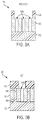
- FIG. 3A depicts a cross-sectional view of the resistor structure after removing the dummy fins and forming trenches according to embodiments of the present invention
- FIG. 3B depicts a cross-sectional view of the FET structure after removing a dummy fin and forming a trench according to embodiments of the present invention
- FIG. 4A depicts a cross-sectional view of the resistor structure after depositing a first material into the trenches according to embodiments of the present invention
- FIG. 4B depicts a cross-sectional view of the FET structure after depositing a first material into the trench according to embodiments of the present invention
- FIG. 5A depicts a cross-sectional view of the resistor structure after removing portions of the first material according to embodiments of the present invention
- FIG. 5B depicts a cross-sectional view of the FET structure after removing portions of the first material according to embodiments of the present invention
- FIG. 6A depicts a cross-sectional view of the resistor structure after depositing a second material to form resistor fins according to embodiments of the present invention
- FIG. 6B depicts a cross-sectional view of the FET structure after depositing a second material to form a resistor fin according to embodiments of the present invention
- FIG. 7A depicts a cross-sectional view of the resistor structure after removing portions of the shallow trench isolation (STI) layer according to embodiments of the present invention
- FIG. 7B depicts a cross-sectional view of the FET structure after removing portions of the STI layer according to embodiments of the present invention
- FIG. 8A depicts a top-down view of the resistor structure showing exposed resistor fins according to embodiments of the present invention
- FIG. 8B depicts a top-down view of the FET structure showing an exposed resistor fin and after forming a gate according to embodiments of the present invention
- FIG. 8C depicts a cross-sectional view of the FET structure showing an exposed resistor fin and source/drain regions according to embodiments of the present invention
- FIG. 8D depicts a cross-sectional view of the FET structure showing a resistor fin and a gate according to embodiments of the present invention
- FIG. 9A depicts a cross-sectional view of the resistor structure after depositing STI material according to embodiments of the present invention.
- FIG. 9B depicts a cross-sectional view of the FET structure after depositing STI material according to embodiments of the present invention.
- FIG. 10A depicts a cross-sectional view of the resistor structure after depositing a hard mask according to embodiments of the present invention
- FIG. 10B depicts a cross-sectional view of the FET structure after depositing a hard mask according to embodiments of the present invention
- FIG. 11A depicts a top-down view of completed resistor fins on a semiconductor structure after creating recesses and adding a metal contact layer according to embodiments of the present invention
- FIG. 11B depicts a cross-sectional view of completed resistor fins on a semiconductor structure according to embodiments of the present invention
- FIG. 11C depicts a top-down view of the completed resistor fin with a FET structure after creating recesses and adding a metal contact layer according to embodiments of the present invention
- FIG. 11D depicts a cross-sectional view of the completed resistor fin with a FET structure depicted in FIG. 11C according to embodiments of the present invention
- FIG. 12 is a flow chart of a method for forming resistor fins on a substrate according to embodiments of the present invention.
- FIG. 13 is a flow chart of a method of forming a resistor device and field-effect-transistor on a substrate according to embodiments of the present invention.
- references in the present description to forming layer “A” over layer “B” include situations in which one or more intermediate layers (e.g., layer “C”) is between layer “A” and layer “B” as long as the relevant characteristics and functionalities of layer “A” and layer “B” are not substantially changed by the intermediate layer(s).
- layer “C” one or more intermediate layers
- compositions comprising, “comprising,” “includes,” “including,” “has,” “having,” “contains” or “containing,” or any other variation thereof, are intended to cover a non-exclusive inclusion.
- a composition, a mixture, process, method, article, or apparatus that comprises a list of elements is not necessarily limited to only those elements but can include other elements not expressly listed or inherent to such composition, mixture, process, method, article, or apparatus.
- exemplary is used herein to mean “serving as an example, instance, or illustration.” Any embodiment or design described herein as “exemplary” is not necessarily to be construed as preferred or advantageous over other embodiments or designs.
- the term “one or more” is understood to include any integer number greater than or equal to one, i.e. one, two, three, four, etc.
- the term “a plurality” is understood to include any integer number greater than or equal to two, i.e. two, three, four, five, etc.
- connection can include an indirect “connection” and a direct “connection”.
- references in the specification to “one embodiment,” “an embodiment,” “an example embodiment,” etc., indicate that the embodiment described can include a particular feature, structure, or characteristic, but every embodiment can include the particular feature, structure, or characteristic. Moreover, such phrases are not necessarily referring to the same embodiment. Further, when a particular feature, structure, or characteristic is described in connection with an embodiment, it is submitted that it is within the knowledge of one skilled in the art to affect such feature, structure, or characteristic in connection with other embodiments whether or not explicitly described.
- the terms “upper,” “lower,” “right,” “left,” “vertical,” “horizontal,” “top,” “bottom,” and derivatives thereof shall relate to the described structures and methods, as oriented in the drawing figures.
- the terms “overlying,” “atop,” “on top,” “positioned on” or “positioned atop” mean that a first element, such as a first structure, is present on a second element, such as a second structure, where intervening elements such as an interface structure can be present between the first element and the second element.
- the term “direct contact” means that a first element, such as a first structure, and a second element, such as a second structure, are connected without any intermediary conducting, insulating or semiconductor layers at the interface of the two elements.
- the term “selective to,” such as, for example, “a first element selective to a second element,” means that the first element can be etched and the second element can act as an etch stop.
- Deposition is any process that grows, coats, or otherwise transfers a material onto the wafer.
- Available technologies include physical vapor deposition (PVD), chemical vapor deposition (CVD), electrochemical deposition (ECD), molecular beam epitaxy (MBE) and more recently, atomic layer deposition (ALD) among others.
- Removal/etching is any process that removes material from the wafer. Examples include etch processes (either wet or dry), and chemical-mechanical planarization (CMP), and the like.
- Semiconductor doping is the modification of electrical properties by doping, for example, transistor sources and drains, generally by diffusion and/or by ion implantation. These doping processes are followed by furnace annealing or by rapid thermal annealing (RTA). Annealing serves to activate the implanted dopants. Films of both conductors (e.g., poly-silicon, aluminum, copper, etc.) and insulators (e.g., various forms of silicon dioxide, silicon nitride, etc.) are used to connect and isolate transistors and their components. Selective doping of various regions of the semiconductor substrate allows the conductivity of the substrate to be changed with the application of voltage.
- RTA rapid thermal annealing
- Semiconductor lithography is the formation of three-dimensional relief images or patterns on the semiconductor substrate for subsequent transfer of the pattern to the substrate.
- the patterns are formed by a light sensitive polymer called a photo-resist.
- lithography and etch pattern transfer steps are repeated multiple times. Each pattern being printed on the wafer is aligned to the previously formed patterns and slowly the conductors, insulators and selectively doped regions are built up to form the final device.
- resistors onto a substrate in the form of resistor fins are methods and structures for forming resistors onto a substrate in the form of resistor fins.
- the motivation for the present invention includes the ability to simultaneously form, and using the same processes to fabricate, resistor fins with CMOS devices, thus minimizing the number of needed process steps.
- the present methods allow for the formation of resistors on a substrate as an alternative to using poly-resistors or MOL resistors.
- Embodiments described herein include removing only portions of a first resistive material and replacing the first material with a second insulator material to form resistor fins. By depositing and then removing only portions of the first material, resistor fins of a specific predetermined resistance range can be formed.
- forming resistor fins as described herein allow for interconnections with CMOS devices using the same dies and metallized deposition layers, thus increasing reliability when forming and connecting resistor fins to CMOS devices.
- FIG. 1A depicts a cross-sectional view of a resistor fin structure 100 (resistor structure) at an intermediate stage of being formed on a substrate 102
- FIG. 1B depicts a cross-sectional view of a FET structure 200 at an intermediate stage of being formed on the substrate 102
- the resistor structure 100 and the FET structure 200 are configured such that they are constructed from the same types of elements (e.g., fins, STI regions, hardmasks, etc.).
- elements of the resistor structure 100 that are of substantially the same type as elements of the FET structure 200 can be formed on the substrate 102 at substantially the same time using substantially the same fabrication processes.
- the resistor structure 100 and the FET structure 200 include substantially the same types of elements and have been formed on the substrate 102 at this stage of fabrication using the same fabrication processes.
- elements of the resistor structure 100 that are of the same type as elements of the FET structure 200 will be provided with the same reference number.
- the fabrication process described for elements of the resistor structure 100 that are of the same type as elements of the FET structure 200 apply equally to the FET structure 200 .
- the fabrication process described for elements of the FET structure 200 that are of the same type as elements of the resistor structure 100 apply equally to the resistor structure 100 .
- the resistor structure 100 includes the substrate 102 , one or more dummy fins 104 , a layer of STI material 106 , and a fin hard mask 108 .
- Three dummy fins 104 are illustrated in FIG. 1A . However, for ease of illustration, only one dummy fin 104 is provided with a reference number.
- the substrate 102 can include silicon, germanium, silicon germanium, silicon carbide, and those consisting essentially of III-V compound semiconductors. Other suitable substrates 102 include II-VI compound semiconductors.
- the substrate 102 can also include an organic semiconductor or a layered semiconductor such as, for example, Si/SiGe, a silicon-on-insulator, or a SiGe-on-insulator. A portion or the entire substrate 102 can be amorphous, polycrystalline, or monocrystalline. The substrate 102 can be doped or undoped, or contain doped regions and undoped regions therein. In one or more embodiments of the present invention, the dummy fins 104 are made of the same materials as the substrate 102 , but other embodiments are possible.
- the STI material 106 is deposited onto the resistor structure 100 and can be made of a flowable oxide.
- the fin hard mask 108 can be made of silicon nitride (SiN). In yet other embodiments, the fin hard mask 108 can be formed from the same material as the substrate 102 .
- the STI material 106 is used in integrated circuits to prevent electric current leakage between adjacent semiconductor device components.
- STI is generally used in CMOS process technology nodes of 250 nanometers and smaller. Older CMOS technologies and non-MOS technologies commonly use isolation based on “local oxidation of silicon” (LOCOS).
- LOC local oxidation of silicon
- STI is created early during the semiconductor device fabrication process before transistors or other devices are formed.
- the key steps of the STI deposition process involves etching a pattern of trenches in the silicon, depositing one or more dielectric materials (such as silicon dioxide) to fill the trenches, and removing the excess dielectric using a technique such as chemical-mechanical planarization.
- FIG. 1B depicts a cross-sectional view of a FET structure 200 that incorporates a resistor fin according to one or more embodiments of the present invention.
- FIG. 1B uses the same reference numbers and the same or similar processes as shown in FIG. 1A as appropriate.
- the dummy fins 104 can be doped with p-type dopants and/or n-type dopants to be utilized in a p-type FET or an n-type FET. It should be noted that the dummy fins 104 are only considered to be dummy fins (i.e., sacrificial fins) in the resistor structure 100 .
- the dummy fins 104 are not dummy fins but rather are the actual fins utilized to transmit the electron or hole current between the source and drain as understood by one skilled in the art. Although one dummy fin 104 is sacrificed, the other fins 104 remain in the FET structure 200 .
- forming elements of the resistor structure 100 and the FET structure 200 on the substrate 102 can be performed at the same time using the same or similar processes. In the following figures, only those differences between resistor structure 100 and FET structure 200 will be illustrated.
- a first hard mask 110 is placed over the top of the resistor structure 100 .
- the first hard mask 110 defines various openings, including first open region 112 A. Once the first hard mask 110 has been deposited, exposed first open region 112 A defines areas of the resistor structure 100 not protected from a future removal process.
- a first hard mask pattern isolates areas that are pre-selected to remain while allowing other areas (e.g., fin hard mask 108 and dummy fins 104 ) to be exposed to a future removal process as shown in subsequent figures.
- the first hard mask 110 has been deposited onto the FET structure 200 , thus defining a second open region 112 B and exposing a dummy fin 104 to a future removal process as shown in subsequent figures. It should be appreciated that the other dummy fins 104 will remain in the FET structure 200 .
- a mask pattern is placed over the resistor structure 100 and an etching process is performed.
- Methods of etching to remove material from the resistor structure 100 include gas phase hydrofluoric acid (HCl) and a wet etch process with an etchant containing ammonia and hydrogen peroxide.
- the etching process can include, but is not limited to, a directional anisotropic reactive-ion etching (RIE) process.
- RIE reactive-ion etching
- Embodiments of the present invention are not limited as to the specific process applied for etching the structure, and other processes are possible.
- the etching process removes the fin hard mask 108 (of FIG. 2A ) and dummy fins 104 (of FIG.
- the etching process after removing material from the resistor structure 100 , also creates a plurality of first trenches 114 A that are located between the remaining STI material 106 in the spaces previously occupied by the dummy fins 104 and extends downwards to the substrate 102 .
- the first trenches 114 A define spaces where the resistor fins will be fabricated in a future process as described herein.
- FIG. 3B depicts a cross-sectional view of the FET structure 200 after removing a dummy fin 104 and forming a second trench 114 B according to one or more embodiments of the present invention.
- FIG. 3B is a continuation of the processes shown in FIG. 2B .
- An etching process removes the fin hard mask 108 and a dummy fin 104 (of FIG. 2B ) down to a top surface of the substrate 102 .
- the etching process after removing material from the resistor structure 100 , also creates a second trench 114 B that is located between the remaining STI material 106 in the spaces where the dummy fin 104 previously occupied, and extends downwards to the substrate 102 .
- the second trench 114 B defines a space where the resistor fin will be fabricated in a future process as described herein.
- FIG. 4A depicts a cross-sectional view of the resistor structure 100 after removing the first hard mask 110 (of FIG. 3A ) and depositing a first material 116 into the first trenches 114 A (of FIG. 3A ) according to one or more embodiments of the present invention.
- FIG. 4A is a continuation of the processes illustrated in FIG. 3A .
- the first material 116 is conformally deposited onto the resistor structure 100 in a uniform layer.
- the first material 116 fills the first trenches 114 A (of FIG. 3A ) that were formed by the removal process described earlier.
- First material 116 is formed of, but is not limited to, doped polysilicon (Si) that has resistive characteristics based on the volume and height, width, and length dimensions of the first material 116 as formed.
- a planarization process is conducted to remove excess overfill of the first material 116 from the top surface of the resistor structure 100 .
- FIG. 4B depicts a cross-sectional view of the FET structure 200 after removing the first hard mask 110 (of FIG. 3B ) and depositing a first material 116 into the second trench 114 B (of FIG. 3B ) according to one or more embodiments of the present invention.
- FIG. 4B is a continuation of the processes shown in FIG. 3B .
- the first material 116 is conformally deposited onto the FET structure 200 in a uniform layer.
- the first material 116 fills the second trench 114 B (of FIG. 3B ) that was formed by the removal process described earlier.
- First material 116 is formed of, but is not limited to, doped polysilicon (Si) that has resistive characteristics based on the volume and height, width, and length dimensions of the first material 116 as formed.
- a planarization process is conducted to remove excess overfill of the first material 116 from the top surface of the FET structure 200 .
- FIG. 5A depicts a cross-sectional view of the resistor structure 100 after removing portions of the first material 116 according to one or more embodiments of the present invention.
- FIG. 5A is a continuation of the processes illustrated in FIG. 4A .
- the resistor structure 100 is shown after removing portions of the first material 116 by the same or a different removal process as shown in FIG. 3A .
- a plurality of third trenches 115 A are formed after conducting the removal process.
- the third trenches 115 A are in the same location as the first trenches 114 A shown in FIG. 3A , although in the present figure the third trenches 115 A are partially filled with a quantity of first material 116 .
- the third trenches 115 A are present between the STI material 106 and over the remaining first material 116 .
- the third trenches 115 A provide spaces for the deposition of additional layers of material as illustrated in the following figures.
- FIG. 5B depicts a cross-sectional view of the FET structure 200 after removing portions of the first material 116 according to one or more embodiments of the present invention.
- FIG. 5B is a continuation of the processes shown in FIG. 4B .
- the FET structure 200 is shown after removing portions of the first material 116 by the same or a different removal process as shown in FIG. 3A .
- a fourth trench 115 B is formed.
- the fourth trench 115 B is in the same location as the second trench 114 B shown in FIG. 3B , although in the present figure the fourth trench 115 B is partially filled with a quantity of first material 116 .
- the fourth trench 115 B is present in the STI material 106 and over the remaining first material 116 .
- the fourth trench 115 B provides space for the deposition of additional layers of material as illustrated in the following figures.
- FIG. 6A depicts a cross-sectional view of the resistor structure 100 after depositing a second material 118 to form a plurality of first resistor fins 120 A according to one or more embodiments of the present invention.
- FIG. 6A is a continuation of the processes illustrated in FIG. 5A .
- the second material 118 is conformally deposited on top of the first material 116 , and a planarization process is conducted to remove excess overfill of the second material 118 from the top surface of the resistor structure 100 .
- Suitable materials for the second material 118 include, but are not limited to, silicon-carbon-oxide (SiCO).
- the first material 116 and the second material 118 form a plurality of resistor fins 120 A as shown in subsequent figures.
- the second material 118 is an electrical insulator used to isolate the resistor fins 120 A from the surrounding resistor structure 100 .
- the resulting resistor structure 100 includes the substrate 102 , the plurality of resistor fins 120 A formed from first material 116 and second material 118 , and STI material 106 .
- FIG. 6B depicts a cross-sectional view of the FET structure 200 after depositing the second material 118 to form a second resistor fin 120 B according to one or more embodiments of the present invention.
- the second resistor fin 120 B includes the first material 116 and the second material 118 in the FET structure 200 .
- FIG. 6B is a continuation of the processes shown in FIG. 5B .
- the second material 118 is conformally deposited on top of the first material 116 .
- the second material 118 is formed of, but is not limited to, SiCO. Combined, the first material 116 and the second material 118 make up the materials to form the second resistor fin 120 B as shown in the following figures.
- the second material 118 is an electrical insulator used to isolate the second resistor fin 120 B from the surrounding FET structure 200 .
- a planarization process is conducted to remove excess overfill of the second material 118 from the top surface of the FET structure 200 .
- the resulting FET structure 200 includes the substrate 102 with the second resistor fin 120 B exhibiting an extended length and formed of first material 116 and second material 118 and surrounded by STI material 106 .
- FIG. 7A depicts a cross-sectional view of the resistor structure 100 after removing portions of the STI material 106 by the same or a different etching process as illustrated in FIG. 3A , thus producing one or more first void regions 117 .
- the second material 118 acts as a hard mask to protect the first material 116 during the etching process.
- FIG. 7B depicts a cross-sectional view of the FET structure 200 after removing portions of the STI material 106 by the same or a different etching process as illustrated in FIG. 3B , thus producing one or more second void regions 119 .
- portions of the second resistor fin 120 B is exposed.
- fins 104 formed of the substrate 102 are exposed by the second void regions 119 .
- the fins 104 extending up from the substrate 102 are on both sides of the second resistor fin 120 B.
- FIG. 8A depicts a top-down view of the resistor structure 100 showing exposed second resistor fins 120 A over the STI material 106 .
- the STI material 106 is positioned over the substrate 102 .
- the second material 118 of the second resistor fins 120 A is seen from the top-down view.
- FIG. 8B depicts a top-down view of the FET structure 200 after forming one or more gate structures 134 (gate) first and an epitaxially growing source/drain region 130 (source/drain or S/D) on top surface of the FET structure 200 .
- the second resistor fin 120 B is also shown.
- the one or more gates 134 are only formed in the FET structure 200 and not on the resistor structure 100 .
- the gates 134 are formed in a pattern that covers a selected part of the second resistor fin 120 B and the fins 104 .
- the source/drain region 130 is expitaxilly grown on the fins 104 formed of the substrate 102 (previously exposed by the second void regions 119 ).
- the source/drain region 130 is not formed on the second resistor fin 120 B in the FET structure 200 .
- the gates 134 includes a high-k gate dielectric and a gate conductor.
- the gate 134 can be, but is not limited to, made of silicon oxide, silicon nitride, silicon oxynitride, boron nitride, high-k materials, or any combination of these materials.
- Arbitrary cut lines A-A′ and B-B′ of the FET structure 200 are shown in more detail in the following figures.
- Epitaxial materials can be grown from gaseous or liquid precursors. Epitaxial materials can be grown using vapor-phase epitaxy (VPE), molecular-beam epitaxy (MBE), liquid-phase epitaxy (LPE), or other suitable process.
- VPE vapor-phase epitaxy
- MBE molecular-beam epitaxy
- LPE liquid-phase epitaxy
- Epitaxial silicon, silicon germanium, and/or carbon doped silicon (SiC) silicon can be doped during deposition (in-situ doped) by adding dopants, n-type dopants (e.g., phosphorus or arsenic) or p-type dopants (e.g., boron or gallium), depending on the type of transistor.
- dopants e.g., phosphorus or arsenic
- p-type dopants e.g., boron or gallium
- epitaxial growth and/or deposition and “epitaxially formed and/or grown” mean the growth of a semiconductor material (crystalline material) on a deposition surface of another semiconductor material (crystalline material), in which the semiconductor material being grown (crystalline overlayer) has substantially the same crystalline characteristics as the semiconductor material of the deposition surface (seed material).
- the chemical reactants provided by the source gases are controlled and the system parameters are set so that the depositing atoms arrive at the deposition surface of the semiconductor substrate with sufficient energy to move about on the surface such that the depositing atoms orient themselves to the crystal arrangement of the atoms of the deposition surface.
- an epitaxially grown semiconductor material has substantially the same crystalline characteristics as the deposition surface on which the epitaxially grown material is formed.
- an epitaxially grown semiconductor material deposited on a ⁇ 100 ⁇ orientated crystalline surface will take on a ⁇ 100 ⁇ orientation.
- epitaxial growth and/or deposition processes are selective to forming on semiconductor surface, and generally do not deposit material on exposed surfaces, such as silicon dioxide or silicon nitride surfaces.
- the gas source for the deposition of epitaxial semiconductor material include a silicon containing gas source, a germanium containing gas source, or a combination thereof.
- a silicon gas source that is selected from the group consisting of silane, disilane, trisilane, tetrasilane, hexachlorodisilane, tetrachlorosilane, dichlorosilane, trichlorosilane, methylsilane, dimethylsilane, ethylsilane, methyldisilane, dimethyldisilane, hexamethyldisilane and combinations thereof.
- An epitaxial germanium layer can be deposited from a germanium gas source that is selected from the group consisting of germane, digermane, halogermane, dichlorogermane, trichlorogermane, tetrachlorogermane and combinations thereof. While an epitaxial silicon germanium alloy layer can be formed utilizing a combination of such gas sources. Carrier gases like hydrogen, nitrogen, helium and argon can be used.
- high-k materials include, but are not limited to, metal oxides such as hafnium oxide, hafnium silicon oxide, hafnium silicon oxynitride, lanthanum oxide, lanthanum aluminum oxide, zirconium oxide, zirconium silicon oxide, zirconium silicon oxynitride, tantalum oxide, titanium oxide, barium strontium titanium oxide, barium titanium oxide, strontium titanium oxide, yttrium oxide, aluminum oxide, lead scandium tantalum oxide, and lead zinc niobate.
- the high-k gate 134 material can further include dopants such as lanthanum and aluminum.
- the gate conductor material can include doped polycrystalline or amorphous silicon, germanium, silicon germanium, a metal (e.g., tungsten, titanium, tantalum, ruthenium, zirconium, cobalt, copper, aluminum, lead, platinum, tin, silver, or gold), a conducting metallic compound material (e.g., tantalum nitride, titanium nitride, tantalum carbide, titanium carbide, titanium aluminum carbide, tungsten silicide, tungsten nitride, ruthenium oxide, cobalt silicide, or nickel silicide), carbon nanotube, conductive carbon, graphene, or any suitable combination of these materials.
- a metal e.g., tungsten, titanium, tantalum, ruthenium, zirconium, cobalt, copper, aluminum, lead, platinum, tin, silver, or gold
- a conducting metallic compound material e.g., tantalum nitride, titanium nitride,
- the conductive material can further include dopants that are incorporated during or after deposition.
- the gate 134 can further include a work function setting layer.
- the work function layer can be a nitride, including but not limited to titanium nitride (TiN), hafnium nitride (HfN), hafnium silicon nitride (HfSiN), tantalum nitride (TaN), tantalum silicon nitride (TaSiN), tungsten nitride (WN), molybdenum nitride (MoN), niobium nitride (NbN); a carbide, including but not limited to titanium carbide (TiC) titanium aluminum carbide (TiAlC), tantalum carbide (TaC), hafnium carbide (HfC), and combinations thereof.
- FIG. 8C depicts a cross-sectional view of the FET structure 200 showing an exposed second resistor fin 120 B and epitaxially-grown source/drain regions 130 according to one or more embodiments of the present invention.
- FIG. 8C is a continuation of the processes shown in FIG. 8B and shows the cross-sectional view at the cut line A-A′ of FIG. 8B .
- FIG. 8C includes the second resistor fin 120 B on the substrate 102 as shown in FIG. 8B .
- FIG. 8D depicts a cross-sectional view of the FET structure 200 showing the second resistor fin 120 B and a gate 134 according to one or more embodiments of the present invention.
- FIG. 8D is a continuation of the processes shown in FIG. 8B and shows the cross-sectional view at the cut line B-B′ of FIG. 8B .
- FIG. 9A depicts a cross-sectional view of the resistor structure 100 after depositing a STI material 106 according to one or more embodiments of the present invention.
- FIG. 9A is a continuation of the processes illustrated in FIG. 8A .
- an additional layer of STI material 106 is deposited onto the resistor structure 100 and surrounding the resistor fins 120 A.
- FIG. 9B depicts a cross-sectional view of the FET structure 200 after depositing a STI material 106 according to one or more embodiments of the present invention.
- FIG. 9B is a continuation of the processes shown in FIG. 8B .
- an additional layer of STI material 106 is deposited onto the FET structure 200 .
- the additional layer of STI material 106 is deposited to surround the source/drains 130 and the second resistor fin 120 B.
- FIG. 10A depicts a cross-sectional view of the resistor structure 100 after depositing a second hard mask 124 according to one or more embodiments of the present invention.
- FIG. 10A is a continuation of FIG. 9A .
- the second hard mask 124 is deposited onto the resistor structure 100 using a deposition process as shown in FIG. 2A .
- a separate deposition process is used to apply the second hard mask 124 .
- a first recess region 122 A (first recess) is created that is devoid of material and defines areas that are exposed to a future etching process.
- the second hard mask 124 can be a photoresist.
- FIG. 10B depicts a cross-sectional view of the FET structure 200 after depositing second hard mask 124 ′ according to one or more embodiments of the present invention.
- FIG. 10B is a continuation of the processes shown in FIG. 9B .
- the second hard mask 124 ′ is deposited onto the FET structure 200 using a deposition process as shown in FIG. 2A .
- a second recess region 122 B (second recess) is created that defines an area that are exposed to a future etching process.
- a separate etch process is utilized to open the second recess region 122 B in FET structure 200 than to open the first recess region 122 A in the resistor structure 100 .
- FIG. 11A depicts a top-down view of the completed resistor structure 100 after adding a metal contact layer 126 according to one or more embodiments of the present invention.
- FIG. 11A is a continuation of FIG. 10A .
- an etching process is conducted to remove portions of the STI material 106 from the resistor structure 100 .
- the resistor structure 100 is partially covered by the second hard mask 124 .
- the purpose of the second hard mask 124 and the etching process that follows is to define/etch an area in the STI material 106 (of FIG. 10A ) where the metal contact layer 126 (metal contacts) are to be deposited.
- the etching process causes STI material 106 to be removed and causes the second material 118 to be removed so that the first material 116 is exposed.
- this etching process occurs at only predefined locations on the first resistor fins 120 A in the resistor structure 100 .
- two material contacts 126 are formed on the exposed areas of the first material.
- the second hard mask 124 is removed.
- the two metal contacts 126 are electrically connected to the resistor fins 120 A (on the first material 116 ) for use in a semiconductor structure device as required.
- the metal contacts 126 will be located at the longitudinal ends of the resistor fins 120 A.
- the first resistor fins 120 A are covered by the STI material 106 and only hidden lines are shown to represent the covered first resistor fins 120 A.
- an optional planarization process can be performed to reduce the height of the metal contacts 126 .
- the metal contacts 126 can further include a work function setting layer (not shown).
- the work function setting layer can be a nitride, including but not limited to titanium nitride (TiN), hafnium nitride (HfN), hafnium silicon nitride (HfSiN), tantalum nitride (TaN), tantalum silicon nitride (TaSiN), tungsten nitride (WN), molybdenum nitride (MoN), niobium nitride (NbN); a carbide, including but not limited to titanium carbide (TiC) titanium aluminum carbide (TiAlC), tantalum carbide (TaC), hafnium carbide (HfC), and combinations thereof.
- TiN titanium nitride
- HfN hafnium nitride
- HfSiN hafnium silicon nitride
- TaN tantalum nitride
- TaSiN tantalum silicon nitride
- FIG. 11B depicts a cross-sectional view of the completed resistor structure 100 depicted in FIG. 11A according to one or more embodiments of the present invention.
- FIG. 11B is a continuation of the processes illustrated in FIG. 11A .
- FIG. 11B shows another view of the completed resistor structure 100 , with the substrate 102 , the plurality of resistor fins, of which only the first material 116 is shown, and the metal contact 126 .
- the metal contact 126 is formed on the exposed portions of the first material 116 , after the etching process removes STI material 106 and the second material 118 at the predefined locations in the resistor structure 100 .
- FIG. 11C depicts a top-down view of the completed FET structure 200 after creating the resistor fin 120 B and adding the metal contact layers 126 according to one or more embodiments of the present invention.
- FIG. 11C is a continuation of the processes shown in FIG. 10B .
- FIG. 11C also includes an arbitrary cut line B-B′ as illustrated in the following figure.
- the FET structure 200 is partially covered by the second hard mask 124 ′.
- the purpose of the second hard mask 124 ′ (showing second recess region 122 B of FIG. 10B ) and the etching process that follows is to define an area in the STI material 106 where the metal contact layer 126 (metal contacts) are deposited.
- the etching process causes STI material 106 to be removed but does not remove the second material 118 of the second resistor fin 120 B in the FET structure 200 . Therefore, the first material 116 is not exposed in the FET structure 200 . It is noted that a separate etch process is utilized to remove STI material 106 (but not the second material 118 of the second resistor fin 120 B) in the FET structure 200 from the etch process to remove the second material 118 of the first resistor fins 120 A in the resistor device 100 . Subsequently, the metal contact 126 is formed on the source/drain regions 130 but not on the second material 118 of the second resistor fin 120 B.
- FIG. 11D depicts a cross-sectional view of the completed resistor fin 120 B with a FET structure 200 shown in FIG. 11C according to one or more embodiments of the present invention.
- FIG. 11D is a continuation of the processes illustrated in FIG. 10B . This view includes gate 134 , source/drains 130 , and second resistor fin 120 B as shown in the preceding figures.
- metal interconnections can be formed between the resistor fin device 100 and other semiconductor devices on the substrate 102 .
- FIG. 12 depicts a flow chart of method 1200 for forming resistor fins on a substrate 120 according to embodiments of the present invention.
- shallow trench isolation material 106 is formed on dummy fins 104 and the substrate 102 , where the dummy fins 104 are formed on the substrate 102 .
- predefined ones of the dummy fins 104 are removed, thereby forming voids 114 A, 114 B in the shallow trench isolation material 106 corresponding to previous locations of the predefined ones of the dummy fins 104 that were removed.
- a first material 116 is deposited into the voids 114 A, 114 B.
- a height of the first material 116 is reduced, thereby forming trenches 115 A, 115 B in the shallow trench isolation material 106 .
- a second material 118 is deposited into the trenches 115 A, 115 B, where the second material 118 is on top of the first material 116 , thereby forming the resistor fins 120 B of the resistor fin device 100 .
- a metal contact layer 126 is formed so as to contact a top surface of the first material 116 at predefined locations.
- the first material 116 is a resistive material with a resistivity value so as to contact electricity.
- a field-effect-transistor 200 is formed at a same time as form the resistor fin device 100 .
- the field-effect-transistor 200 includes one of the resistor fins 120 B.
- the field-effect-transistor 200 includes source/drain regions 130 formed on other fins 104 .
- the first material 116 includes a doped polysilicon material.
- the second material 118 is an electrically-isolating insulator.
- the metal contact layer 126 includes a work function setting layer.
- FIG. 13 is a flow chart of a method 1300 of forming a resistor device 100 and field-effect-transistor 200 on a substrate 102 according to embodiments of the present invention.
- a shallow trench isolation material 106 formed on sacrificial fins 104 and the substrate 102 , where the sacrificial fins 104 are formed on the substrate 102 .
- the sacrificial fins 104 are removed in the resistor device 100 while removing one of the sacrificial fins 104 in the field-effect-transistor 200 , thereby forming voids 114 A, 114 B in the shallow trench isolation material 106 corresponding to previous locations of the sacrificial fins 104 having been removed.
- a first material 116 is formed into the voids 114 A, 114 B, where the first material 116 has a height that forms trenches 115 A, 115 B in the shallow trench isolation material 106 .
- a second material 118 formed into the trenches 115 A, 115 B, where the second material 118 is on top of the first material 116 .
- a gate 134 and source/drain regions 130 are formed in the field-effect-transistor 200 .
- a metal contact layer 126 is formed so as to contact the first material 116 at predefined locations in the resistor device 100 and to contact source/drain regions 130 in the field-effect-transistor 200 .
- the first material 116 is a doped polysilicon material.
- the second material 118 is an electrically-isolating insulator material.
- the first material 116 is a resistive material with a resistivity value.
- various functions or acts can take place at a given location and/or in connection with the operation of one or more apparatuses or systems.
- a portion of a given function or act can be performed at a first device or location, and the remainder of the function or act can be performed at one or more additional devices or locations.
Landscapes
- Engineering & Computer Science (AREA)
- Physics & Mathematics (AREA)
- Condensed Matter Physics & Semiconductors (AREA)
- General Physics & Mathematics (AREA)
- Manufacturing & Machinery (AREA)
- Computer Hardware Design (AREA)
- Microelectronics & Electronic Packaging (AREA)
- Power Engineering (AREA)
- Semiconductor Integrated Circuits (AREA)
- Metal-Oxide And Bipolar Metal-Oxide Semiconductor Integrated Circuits (AREA)
- Insulated Gate Type Field-Effect Transistor (AREA)
Abstract
Description
Claims (20)
Priority Applications (1)
| Application Number | Priority Date | Filing Date | Title |
|---|---|---|---|
| US15/991,143 US10629589B2 (en) | 2017-04-24 | 2018-05-29 | Resistor fins |
Applications Claiming Priority (2)
| Application Number | Priority Date | Filing Date | Title |
|---|---|---|---|
| US15/495,197 US10079229B1 (en) | 2017-04-24 | 2017-04-24 | Resistor fins |
| US15/991,143 US10629589B2 (en) | 2017-04-24 | 2018-05-29 | Resistor fins |
Related Parent Applications (1)
| Application Number | Title | Priority Date | Filing Date |
|---|---|---|---|
| US15/495,197 Division US10079229B1 (en) | 2017-04-24 | 2017-04-24 | Resistor fins |
Publications (2)
| Publication Number | Publication Date |
|---|---|
| US20180308837A1 US20180308837A1 (en) | 2018-10-25 |
| US10629589B2 true US10629589B2 (en) | 2020-04-21 |
Family
ID=63491115
Family Applications (2)
| Application Number | Title | Priority Date | Filing Date |
|---|---|---|---|
| US15/495,197 Expired - Fee Related US10079229B1 (en) | 2017-04-24 | 2017-04-24 | Resistor fins |
| US15/991,143 Expired - Fee Related US10629589B2 (en) | 2017-04-24 | 2018-05-29 | Resistor fins |
Family Applications Before (1)
| Application Number | Title | Priority Date | Filing Date |
|---|---|---|---|
| US15/495,197 Expired - Fee Related US10079229B1 (en) | 2017-04-24 | 2017-04-24 | Resistor fins |
Country Status (1)
| Country | Link |
|---|---|
| US (2) | US10079229B1 (en) |
Families Citing this family (8)
| Publication number | Priority date | Publication date | Assignee | Title |
|---|---|---|---|---|
| US11461620B2 (en) * | 2017-07-05 | 2022-10-04 | Samsung Electronics Co., Ltd. | Multi-bit, SoC-compatible neuromorphic weight cell using ferroelectric FETs |
| US11404423B2 (en) * | 2018-04-19 | 2022-08-02 | Taiwan Semiconductor Manufacturing Co., Ltd | Fin-based strap cell structure for improving memory performance |
| US10559572B2 (en) | 2018-06-29 | 2020-02-11 | International Business Machines Corporation | Vertical transistor contact for a memory cell with increased density |
| US10566453B2 (en) * | 2018-06-29 | 2020-02-18 | International Business Machines Corporation | Vertical transistor contact for cross-coupling in a memory cell |
| US20200118720A1 (en) * | 2018-10-11 | 2020-04-16 | Texas Instruments Incorporated | Tunable multi-segment thermistor |
| CN111613606B (en) * | 2019-02-22 | 2022-05-10 | 群创光电股份有限公司 | display device |
| US10797046B1 (en) * | 2019-03-29 | 2020-10-06 | GlobalFoundries, Inc. | Resistor structure for integrated circuit, and related methods |
| KR102771900B1 (en) | 2019-12-09 | 2025-02-25 | 삼성전자주식회사 | Resistor with doped regions |
Citations (12)
| Publication number | Priority date | Publication date | Assignee | Title |
|---|---|---|---|---|
| US6582987B2 (en) | 2000-12-30 | 2003-06-24 | Electronics And Telecommunications Research Institute | Method of fabricating microchannel array structure embedded in silicon substrate |
| US6969656B2 (en) | 2003-12-05 | 2005-11-29 | Freescale Semiconductor, Inc. | Method and circuit for multiplying signals with a transistor having more than one independent gate structure |
| US7064413B2 (en) | 2002-01-28 | 2006-06-20 | International Business Machines Corporation | Fin-type resistors |
| US20070128740A1 (en) | 2004-09-17 | 2007-06-07 | International Business Machines Corporation | Polysilicon Conductor Width Measurement for 3-Dimensional FETs |
| US8026521B1 (en) | 2010-10-11 | 2011-09-27 | Monolithic 3D Inc. | Semiconductor device and structure |
| US8816436B2 (en) | 2012-05-16 | 2014-08-26 | International Business Machines Corporation | Method and structure for forming fin resistors |
| US8836032B2 (en) | 2011-10-20 | 2014-09-16 | Broadcom Corporation | Fin-based adjustable resistor |
| US20150061076A1 (en) * | 2013-08-27 | 2015-03-05 | International Business Machines Corporation | High density resistor |
| US20150333057A1 (en) | 2014-05-13 | 2015-11-19 | Globalfoundries Inc. | Meander resistor |
| US9236267B2 (en) | 2012-02-09 | 2016-01-12 | Taiwan Semiconductor Manufacturing Company, Ltd. | Cut-mask patterning process for fin-like field effect transistor (FinFET) device |
| US20160190120A1 (en) | 2014-12-29 | 2016-06-30 | Globalfoundries Inc. | Fin resistor with overlying gate structure |
| US9419004B2 (en) * | 2014-04-03 | 2016-08-16 | Samsung Electronics Co., Ltd. | Fuse structure and semiconductor device including the same |
-
2017
- 2017-04-24 US US15/495,197 patent/US10079229B1/en not_active Expired - Fee Related
-
2018
- 2018-05-29 US US15/991,143 patent/US10629589B2/en not_active Expired - Fee Related
Patent Citations (12)
| Publication number | Priority date | Publication date | Assignee | Title |
|---|---|---|---|---|
| US6582987B2 (en) | 2000-12-30 | 2003-06-24 | Electronics And Telecommunications Research Institute | Method of fabricating microchannel array structure embedded in silicon substrate |
| US7064413B2 (en) | 2002-01-28 | 2006-06-20 | International Business Machines Corporation | Fin-type resistors |
| US6969656B2 (en) | 2003-12-05 | 2005-11-29 | Freescale Semiconductor, Inc. | Method and circuit for multiplying signals with a transistor having more than one independent gate structure |
| US20070128740A1 (en) | 2004-09-17 | 2007-06-07 | International Business Machines Corporation | Polysilicon Conductor Width Measurement for 3-Dimensional FETs |
| US8026521B1 (en) | 2010-10-11 | 2011-09-27 | Monolithic 3D Inc. | Semiconductor device and structure |
| US8836032B2 (en) | 2011-10-20 | 2014-09-16 | Broadcom Corporation | Fin-based adjustable resistor |
| US9236267B2 (en) | 2012-02-09 | 2016-01-12 | Taiwan Semiconductor Manufacturing Company, Ltd. | Cut-mask patterning process for fin-like field effect transistor (FinFET) device |
| US8816436B2 (en) | 2012-05-16 | 2014-08-26 | International Business Machines Corporation | Method and structure for forming fin resistors |
| US20150061076A1 (en) * | 2013-08-27 | 2015-03-05 | International Business Machines Corporation | High density resistor |
| US9419004B2 (en) * | 2014-04-03 | 2016-08-16 | Samsung Electronics Co., Ltd. | Fuse structure and semiconductor device including the same |
| US20150333057A1 (en) | 2014-05-13 | 2015-11-19 | Globalfoundries Inc. | Meander resistor |
| US20160190120A1 (en) | 2014-12-29 | 2016-06-30 | Globalfoundries Inc. | Fin resistor with overlying gate structure |
Non-Patent Citations (3)
| Title |
|---|
| Disclosed Anonymously, "Integrated Ciruits with FinFETs and Resistors," IP.com, IPCOM000241490D, May 5, 2015, pp. 1-3. |
| List of IBM Patents or Patent Applications Treated as Related, (Appendix P), Filed May 29, 2018; pp. 1-2. |
| Zhenxing Bi et al., "Resistor Fins", Related Application, U.S. Appl. No. 15/495,197, filed Apr. 24, 2017. |
Also Published As
| Publication number | Publication date |
|---|---|
| US20180308837A1 (en) | 2018-10-25 |
| US10079229B1 (en) | 2018-09-18 |
Similar Documents
| Publication | Publication Date | Title |
|---|---|---|
| US11705517B2 (en) | Nanosheet transistors with strained channel regions | |
| US10629589B2 (en) | Resistor fins | |
| US10128372B1 (en) | Bottom contact resistance reduction on VFET | |
| US10896972B2 (en) | Self-aligned contact for vertical field effect transistor | |
| US20190157267A1 (en) | Finfets with controllable and adjustable channel doping | |
| US9647120B1 (en) | Vertical FET symmetric and asymmetric source/drain formation | |
| US10833190B2 (en) | Super long channel device within VFET architecture | |
| US20200066711A1 (en) | Integrating a junction field effect transistor into a vertical field effect transistor | |
| US10032679B1 (en) | Self-aligned doping in source/drain regions for low contact resistance | |
| US10431667B2 (en) | Vertical field effect transistors with uniform threshold voltage | |
| US11239342B2 (en) | Vertical transistors having improved control of top source or drain junctions | |
| US10573745B2 (en) | Super long channel device within VFET architecture | |
| US10665694B2 (en) | Vertical transistors having improved gate length control | |
| WO2024060646A1 (en) | Improved epi growth uniformity with source/drain placeholder | |
| US10665715B2 (en) | Controlling gate length of vertical transistors | |
| US20250194140A1 (en) | Multiple fin heights for effective width tuning | |
| US10811508B2 (en) | Vertical transistors having multiple gate thicknesses for optimizing performance and device density |
Legal Events
| Date | Code | Title | Description |
|---|---|---|---|
| AS | Assignment |
Owner name: INTERNATIONAL BUSINESS MACHINES CORPORATION, NEW YORK Free format text: ASSIGNMENT OF ASSIGNORS INTEREST;ASSIGNORS:BI, ZHENXING;CHENG, KANGGUO;LI, JUNTAO;AND OTHERS;REEL/FRAME:045920/0963 Effective date: 20170420 Owner name: INTERNATIONAL BUSINESS MACHINES CORPORATION, NEW Y Free format text: ASSIGNMENT OF ASSIGNORS INTEREST;ASSIGNORS:BI, ZHENXING;CHENG, KANGGUO;LI, JUNTAO;AND OTHERS;REEL/FRAME:045920/0963 Effective date: 20170420 |
|
| FEPP | Fee payment procedure |
Free format text: ENTITY STATUS SET TO UNDISCOUNTED (ORIGINAL EVENT CODE: BIG.); ENTITY STATUS OF PATENT OWNER: LARGE ENTITY |
|
| STPP | Information on status: patent application and granting procedure in general |
Free format text: RESPONSE TO NON-FINAL OFFICE ACTION ENTERED AND FORWARDED TO EXAMINER |
|
| STPP | Information on status: patent application and granting procedure in general |
Free format text: NON FINAL ACTION MAILED |
|
| STPP | Information on status: patent application and granting procedure in general |
Free format text: RESPONSE TO NON-FINAL OFFICE ACTION ENTERED AND FORWARDED TO EXAMINER |
|
| STPP | Information on status: patent application and granting procedure in general |
Free format text: FINAL REJECTION MAILED |
|
| STPP | Information on status: patent application and granting procedure in general |
Free format text: RESPONSE AFTER FINAL ACTION FORWARDED TO EXAMINER |
|
| STPP | Information on status: patent application and granting procedure in general |
Free format text: ADVISORY ACTION MAILED |
|
| STPP | Information on status: patent application and granting procedure in general |
Free format text: NOTICE OF ALLOWANCE MAILED -- APPLICATION RECEIVED IN OFFICE OF PUBLICATIONS |
|
| STCF | Information on status: patent grant |
Free format text: PATENTED CASE |
|
| AS | Assignment |
Owner name: ELPIS TECHNOLOGIES INC., CANADA Free format text: ASSIGNMENT OF ASSIGNORS INTEREST;ASSIGNOR:INTERNATIONAL BUSINESS MACHINES CORPORATION;REEL/FRAME:052557/0327 Effective date: 20200306 |
|
| FEPP | Fee payment procedure |
Free format text: MAINTENANCE FEE REMINDER MAILED (ORIGINAL EVENT CODE: REM.); ENTITY STATUS OF PATENT OWNER: LARGE ENTITY |
|
| LAPS | Lapse for failure to pay maintenance fees |
Free format text: PATENT EXPIRED FOR FAILURE TO PAY MAINTENANCE FEES (ORIGINAL EVENT CODE: EXP.); ENTITY STATUS OF PATENT OWNER: LARGE ENTITY |
|
| STCH | Information on status: patent discontinuation |
Free format text: PATENT EXPIRED DUE TO NONPAYMENT OF MAINTENANCE FEES UNDER 37 CFR 1.362 |
|
| STCH | Information on status: patent discontinuation |
Free format text: PATENT EXPIRED DUE TO NONPAYMENT OF MAINTENANCE FEES UNDER 37 CFR 1.362 |
|
| FP | Lapsed due to failure to pay maintenance fee |
Effective date: 20240421 |