US10611632B1 - Singulation of wafer level packaging - Google Patents
Singulation of wafer level packaging Download PDFInfo
- Publication number
- US10611632B1 US10611632B1 US16/236,430 US201816236430A US10611632B1 US 10611632 B1 US10611632 B1 US 10611632B1 US 201816236430 A US201816236430 A US 201816236430A US 10611632 B1 US10611632 B1 US 10611632B1
- Authority
- US
- United States
- Prior art keywords
- wafer
- window assembly
- semiconductor wafer
- integrated circuits
- carrier fixture
- Prior art date
- Legal status (The legal status is an assumption and is not a legal conclusion. Google has not performed a legal analysis and makes no representation as to the accuracy of the status listed.)
- Active
Links
Images


Classifications
-
- B—PERFORMING OPERATIONS; TRANSPORTING
- B81—MICROSTRUCTURAL TECHNOLOGY
- B81C—PROCESSES OR APPARATUS SPECIALLY ADAPTED FOR THE MANUFACTURE OR TREATMENT OF MICROSTRUCTURAL DEVICES OR SYSTEMS
- B81C1/00—Manufacture or treatment of devices or systems in or on a substrate
- B81C1/00865—Multistep processes for the separation of wafers into individual elements
- B81C1/00896—Temporary protection during separation into individual elements
-
- G—PHYSICS
- G02—OPTICS
- G02B—OPTICAL ELEMENTS, SYSTEMS OR APPARATUS
- G02B26/00—Optical devices or arrangements for the control of light using movable or deformable optical elements
- G02B26/08—Optical devices or arrangements for the control of light using movable or deformable optical elements for controlling the direction of light
- G02B26/0816—Optical devices or arrangements for the control of light using movable or deformable optical elements for controlling the direction of light by means of one or more reflecting elements
- G02B26/0833—Optical devices or arrangements for the control of light using movable or deformable optical elements for controlling the direction of light by means of one or more reflecting elements the reflecting element being a micromechanical device, e.g. a MEMS mirror, DMD
-
- B—PERFORMING OPERATIONS; TRANSPORTING
- B81—MICROSTRUCTURAL TECHNOLOGY
- B81B—MICROSTRUCTURAL DEVICES OR SYSTEMS, e.g. MICROMECHANICAL DEVICES
- B81B7/00—Microstructural systems; Auxiliary parts of microstructural devices or systems
- B81B7/0032—Packages or encapsulation
- B81B7/0067—Packages or encapsulation for controlling the passage of optical signals through the package
-
- B—PERFORMING OPERATIONS; TRANSPORTING
- B81—MICROSTRUCTURAL TECHNOLOGY
- B81C—PROCESSES OR APPARATUS SPECIALLY ADAPTED FOR THE MANUFACTURE OR TREATMENT OF MICROSTRUCTURAL DEVICES OR SYSTEMS
- B81C1/00—Manufacture or treatment of devices or systems in or on a substrate
- B81C1/00015—Manufacture or treatment of devices or systems in or on a substrate for manufacturing microsystems
- B81C1/00261—Processes for packaging MEMS devices
- B81C1/00317—Packaging optical devices
-
- B—PERFORMING OPERATIONS; TRANSPORTING
- B81—MICROSTRUCTURAL TECHNOLOGY
- B81C—PROCESSES OR APPARATUS SPECIALLY ADAPTED FOR THE MANUFACTURE OR TREATMENT OF MICROSTRUCTURAL DEVICES OR SYSTEMS
- B81C99/00—Subject matter not provided for in other groups of this subclass
- B81C99/0035—Testing
- B81C99/004—Testing during manufacturing
-
- B—PERFORMING OPERATIONS; TRANSPORTING
- B81—MICROSTRUCTURAL TECHNOLOGY
- B81C—PROCESSES OR APPARATUS SPECIALLY ADAPTED FOR THE MANUFACTURE OR TREATMENT OF MICROSTRUCTURAL DEVICES OR SYSTEMS
- B81C2203/00—Forming microstructural systems
- B81C2203/01—Packaging MEMS
- B81C2203/0118—Bonding a wafer on the substrate, i.e. where the cap consists of another wafer
Definitions
- the packaging process for individual semiconductor dies begins before the semiconductor wafer has been singulated into the individual dies and the dies removed from a chuck on which the semiconductor wafer is adhered. In some cases, the semiconductor wafer is adhered to the chuck and singulated while still on the chuck.
- a packaging material e.g., glass
- a packaging material can then be placed over the semiconductor wafer and further processed as part of the packaging process. It is possible that portions of the semiconductor wafer become damaged while processing the packing material over the wafer. For example, portions of the glass may be removed and the glass portion removal process may result in damage to the underlying semiconductor wafer.
- a method includes, before attaching a window assembly to a semiconductor wafer, the semiconductor wafer including a plurality of integrated circuits and each integrated circuit including an electrical connection pad, adhering the window assembly to a carrier fixture. The method further includes, before attaching the window assembly to the semiconductor wafer, removing portions of the window assembly to create removal areas. The method then includes attaching the window assembly to the semiconductor wafer such that the electrical connection pad of each of the plurality of integrated circuits is within a removal area and removing the carrier fixture leaving the window assembly adhered to the semiconductor wafer with the electrical connection pad exposed of each of the plurality of integrated circuits.
- FIGS. 1-5 illustrate a wafer-level sequence of operations in accordance with an example.
- FIGS. 6-10 illustrate a wafer-level sequence of operations in accordance with another example in which a removable portion is removed in conjunction with removal of the carrier fixture.
- FIGS. 11-16 illustrate a wafer-level sequence of operations in accordance with yet another example.
- FIG. 17 shows a top view of a wafer in accordance with an example.
- FIGS. 18-21 illustrate a wafer-level sequence of operations in accordance with an example of a hermetically bonded structure.
- FIG. 22 shows an example of a wafer level packaging to produce a stacked die structure.
- damage can occur to a semiconductor wafer during wafer level packaging.
- the described examples reduces or avoids such damage by partially modifying a component to be placed over the wafer before the component is actually placed over the wafer. The partially modified component is then adhered to the wafer thereby avoiding the damage that would have otherwise occurred to the wafer.
- FIGS. 1-5 illustrates an example of a time sequence of operations for wafer level processing.
- FIG. 1 illustrates a wafer 100 that is to be adhered to another wafer 130 ( FIG. 3 ).
- wafer 130 is a semiconductor wafer including a plurality of integrated circuits, such as digital micromirror devices (DMDs), and the wafer 100 is a glass (or other type of optically translucent material) wafer.
- the wafer 100 is made from glass and is thus referred to as a window assembly 100 .
- the window assembly 100 includes a glass layer 102 and an interposer 106 .
- the interposer 106 may be made from an optically translucent material such as glass and is adhered to the glass layer by way of, for example, glue or other type of adhesive.
- the interposer 106 functions as a standoff to ensure that the glass layer 102 is not in contact with the underlying wafer 130 , especially not in contact with certain areas of wafer 130 .
- multiple movable mirrors are formed on the surface 131 ( FIG. 3 ) of the wafer 130 and the interposer 106 prevents the glass layer 102 from contacting and damaging the mirrors.
- the interposer 106 does contact wafer 130 but not in areas on the surface 131 of the wafer 130 that includes mirrors or other components that would be damaged by the interposer 106 .
- the window assembly 100 comprises two components (glass layer 102 and interposer 106 ). In other example, however, the window assembly 100 comprises a unitary glass member.
- a carrier fixture 120 is attached to the window assembly as shown in FIG. 1 .
- the carrier fixture 120 is attached to the window assembly by way of a tape 118 .
- All references to the tape 118 herein also includes any type of a temporary adhesive.
- the carrier fixture 120 may be made from metal, plastic, or other suitable material to provide support to the window assembly 100 as it is handled during wafer-level packaging.
- the tape 118 temporarily adheres the window assembly 100 to the carrier fixture 120 so that portions of the window assembly can be removed to create removal areas 110 ( FIG. 2 ).
- the tape can be an ultra-violet (UV) releasable tape meaning that the adhesive capability of the tape is degraded upon exposure to UV light.
- Each removal area 110 is made, for example, by a saw or other type of material removal process.
- the removal area 110 is formed in the window assembly 100 before the window assembly is adhered to the wafer 130 thereby avoiding damage to wafer 130 that might otherwise occur if portions of the window assembly were removed while the window assembly was already
- the window assembly 100 is then adhered to wafer 130 as shown in FIG. 3 .
- the wafer 130 itself may be attached to a chuck 135 to support the wafer during the wafer-level packaging. Glue or other type of adhesive mechanism can be used to adhere the window assembly 100 to the wafer 130 .
- Wafer 130 also includes multiple electrical connection pads such as electrical connection pads 132 and 142 as shown in FIGS. 3-5 . Each electrical pad provides electrical connectivity to an associated integrated circuit formed within wafer 130 .
- FIG. 4 illustrates that carrier fixture 120 has been removed.
- carrier fixture 120 is adhered to the window assembly by way of a temporary adhesive, for example, a UV-releasable tape 118 .
- the tape 118 is exposed to UV light for a suitable period of time.
- the adhesive capability of tape 118 degrades to the point that the carrier fixture 120 can be removed from the window assembly 100 . Absent the carrier fixture 120 , electrical connection pads 132 , 142 are exposed thereby permitting the various integrated circuits (e.g., DMDs) to be electrically tested. The electrical testing is thus performed on the various integrated circuits before the wafer 130 is singulated into individual dies.
- portions of the window assembly 100 would need to be removed to provide access to the electrical connection pads 132 , 142 for testing. Removal of portions of the window assembly 100 while adhered to the wafer might damages the integrated circuits and electrical connections in the areas where the glass comprising the window assembly 100 is being broken off to be removed. By removing portions of the window assembly to create the removal areas 110 before the window assembly 100 is attached to the wafer 130 , such damage is avoided.
- the testing of the individual integrated circuits helps to determine which integrated circuits are acceptable and which are not. Integrated circuits that do not pass the testing can be discarded.
- FIG. 5 illustrates that, following the testing, the wafer 130 is singulated into its individual dies.
- a saw, or type of wafer singulation device, can be used to saw through the wafer 130 .
- FIGS. 6-10 illustrate another example of creating the removal areas in a window assembly.
- two narrower cuts 610 are made through the window assembly 100 as shown.
- cuts 610 are spaced approximately 1 mm apart.
- the portion 620 of the window assembly between the two cuts 610 is a removal portion and may be referred to as a “swizzle stick”.
- the combination of the window assembly 100 and carrier fixture 120 is then adhered to the wafer 130 as shown in FIG. 7 .
- Glue is used to adhere the interposer to the wafer 130 , but glue is not included at the interface between the portion 620 and the wafer 130 .
- FIGS. 8 and 9 illustrate that the tape 118 is deactivated.
- the tape 118 is selectively deactivated. For example, the tape 118 is exposed to UV light at areas of the tape 118 other than at portions 620 .
- the carrier fixture 120 is removed from the window assembly 100 . Because the adhesive capability of the tape 118 is not deactivated at portions 620 , portions 620 are removed along with the carrier fixture as shown in FIG. 9 .
- the electrical connection pads 132 , 142 can be tested as described above, and then the wafer 130 can be singulated into its constituent dies ( FIG. 10 ).
- FIGS. 11-16 illustrate another example of wafer-level packaging.
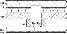
- a carrier fixture 750 is adhered to the window assembly 100 as described above using a releasable (e.g., UV-releasable) tape 118 .
- the window assembly may be temporarily placed on tape 760 .
- the carrier fixture 750 includes cut-outs 755 formed within the surface of the carrier fixture to be adhered to the window assembly 100 .
- FIG. 12 shows that a pair of cuts 780 are made all of the way through the window assembly and into the cut-out 755 . As the cuts 780 are made all of the way through the interposer 106 and glass layer 102 , the portion 785 of the window assembly 100 between the cuts 780 can then be removed as shown in FIG. 13 to create removal areas 790 .
- FIG. 14 that a wafer 130 has been singulated and then the window assembly 100 and carrier fixture 750 adhered to the singulated wafer 800 .
- the individual dies comprising the wafer 800 remain held in place by tape 809 .
- the tape is deactivated (e.g., through exposure to UV light) to thereby permit the carrier fixture 750 to be removed.
- FIG. 16 illustrates that the electrical connection pads 832 and 842 of associated integrated circuits of the individual dies can then be tested.
- FIG. 17 shows an example of top view of a wafer 1600 illustrating multiple integrated circuits 1608 and interposer openings 1615 .
- the interposer openings 1615 cover the integrated circuits 1608 as noted above.
- the glass layer 102 is not specifically shown in the top view for clarity.
- FIGS. 18-21 illustrate wafer-level packaging using hermetic bonding.
- a hermetic bond is any bond that forms a hermetic seal between the window assembly 100 and the wafer 130 , 800 preventing the permeation of gasses into the package.
- the structure 1700 shown in FIGS. 18-21 includes multiple layers including, for example, an interposer 1701 , a thermal oxide layer 1702 , a plasma oxide layer 1704 , and a glass layer 1708 (e.g., borosilicate glass).
- the glass layer 1708 is adhered to a carrier fixture 1712 using an adhesive material 1710 (e.g., tape or other type of temporary adhesive).
- Structures 1730 provide electrical connectivity to contact pads on a semiconductor wafer 1800 ( FIG. 18 ).
- a photoresist layer 1709 is provided as well as shown in FIG. 18 . The photoresist is subsequently removed.
- cuts 1720 and 1725 are made through the stack of the interposer 1701 , thermal oxide layer 1702 , plasma oxide layer 1704 , and the glass layer 1708 into the adhesive material 1710 thereby defining removal portions 1740 .
- Such cuts can be made using a saw or other suitable type of device.
- FIG. 21 illustrates that a semiconductor wafer 1800 is adhered to the structures 1730 . The carrier fixture 1712 can then be removed.
- FIG. 22 illustrates an example of wafer-level packaging involving wafers 2010 and 2020 .
- Each wafer 2010 , 2020 may comprise a semiconductor wafer including one or more integrated circuits, and the wafers are to be bonded together to form a plurality of stacked die structures.
- Wafer 2020 is shown attached to a carrier fixture 2024 by way of adhesive 2022 .
- Wafer 2020 is singulated while on the carrier fixture 2024 via cuts made at 2023 and 2027 but the singulated portions of wafer 2020 remain held in place on the carrier fixture 2024 due to the adhesive 2022 .
- the wafer 2010 is then bonded to wafer 2020 .
- Wafer 2010 then can be singulated at or near the cuts to wafer 2020 made at 2023 and 2027 to thereby form multiple stacked die structures. Because wafer 2020 was singulated while retained in place on the carrier fixture 2024 and because wafer 2010 is adhered to the singulated dies of wafer 2020 , the wafer-level packaging of FIG. 22 does not require any pick-and-place of individual dies onto wafer 2020 , and is thus a faster and more efficient process than if wafer 2010 had already been singulated and pick-and-place was needed to form the stacked structures.
- the stacked dies may then be removed from the carrier fixture 2024 .
- the resulting structures may be attached to a leadframe and then a mold compound may be used to partially or fully encapsulate the dies.
- a mold compound may be used to partially or fully encapsulate the dies.
- the mirror array remains optically exposed through the window assembly 100 .
Landscapes
- Engineering & Computer Science (AREA)
- Microelectronics & Electronic Packaging (AREA)
- Manufacturing & Machinery (AREA)
- Physics & Mathematics (AREA)
- General Physics & Mathematics (AREA)
- Optics & Photonics (AREA)
- Computer Hardware Design (AREA)
- Container, Conveyance, Adherence, Positioning, Of Wafer (AREA)
- Dicing (AREA)
Abstract
A method includes, before attaching a window assembly to a semiconductor wafer, the semiconductor wafer including a plurality of integrated circuits and each integrated circuit including an electrical connection pad, adhering the window assembly to a carrier fixture. The method further includes, before attaching the window assembly to the semiconductor wafer, removing portions of the window assembly to create removal areas. The method then includes attaching the window assembly to the semiconductor wafer such that the electrical connection pad of each of the plurality of integrated circuits is within a removal area and removing the carrier fixture leaving the window assembly adhered to the semiconductor wafer with the electrical connection pad exposed of each of the plurality of integrated circuits.
Description
In wafer level packaging, the packaging process for individual semiconductor dies begins before the semiconductor wafer has been singulated into the individual dies and the dies removed from a chuck on which the semiconductor wafer is adhered. In some cases, the semiconductor wafer is adhered to the chuck and singulated while still on the chuck. A packaging material (e.g., glass) can then be placed over the semiconductor wafer and further processed as part of the packaging process. It is possible that portions of the semiconductor wafer become damaged while processing the packing material over the wafer. For example, portions of the glass may be removed and the glass portion removal process may result in damage to the underlying semiconductor wafer.
In some examples, a method includes, before attaching a window assembly to a semiconductor wafer, the semiconductor wafer including a plurality of integrated circuits and each integrated circuit including an electrical connection pad, adhering the window assembly to a carrier fixture. The method further includes, before attaching the window assembly to the semiconductor wafer, removing portions of the window assembly to create removal areas. The method then includes attaching the window assembly to the semiconductor wafer such that the electrical connection pad of each of the plurality of integrated circuits is within a removal area and removing the carrier fixture leaving the window assembly adhered to the semiconductor wafer with the electrical connection pad exposed of each of the plurality of integrated circuits.
For a detailed description of various examples, reference will now be made to the accompanying drawings in which:
As noted above, damage can occur to a semiconductor wafer during wafer level packaging. The described examples reduces or avoids such damage by partially modifying a component to be placed over the wafer before the component is actually placed over the wafer. The partially modified component is then adhered to the wafer thereby avoiding the damage that would have otherwise occurred to the wafer.
A carrier fixture 120 is attached to the window assembly as shown in FIG. 1 . The carrier fixture 120 is attached to the window assembly by way of a tape 118. All references to the tape 118 herein also includes any type of a temporary adhesive. The carrier fixture 120 may be made from metal, plastic, or other suitable material to provide support to the window assembly 100 as it is handled during wafer-level packaging. The tape 118 temporarily adheres the window assembly 100 to the carrier fixture 120 so that portions of the window assembly can be removed to create removal areas 110 (FIG. 2 ). The tape can be an ultra-violet (UV) releasable tape meaning that the adhesive capability of the tape is degraded upon exposure to UV light. Each removal area 110 is made, for example, by a saw or other type of material removal process. The removal area 110 is formed in the window assembly 100 before the window assembly is adhered to the wafer 130 thereby avoiding damage to wafer 130 that might otherwise occur if portions of the window assembly were removed while the window assembly was already adhered to the wafer 130.
After the removal areas 110 are formed in the window assembly, the window assembly 100 is then adhered to wafer 130 as shown in FIG. 3 . The wafer 130 itself may be attached to a chuck 135 to support the wafer during the wafer-level packaging. Glue or other type of adhesive mechanism can be used to adhere the window assembly 100 to the wafer 130. Wafer 130 also includes multiple electrical connection pads such as electrical connection pads 132 and 142 as shown in FIGS. 3-5 . Each electrical pad provides electrical connectivity to an associated integrated circuit formed within wafer 130.
The testing of the individual integrated circuits helps to determine which integrated circuits are acceptable and which are not. Integrated circuits that do not pass the testing can be discarded.
The examples described above represent epoxy-based wafer-level packaging in that an epoxy-based adhesive may be used to adhere the carrier fixture 120, 750 to the window assembly 100 and to adhere the window assembly 100 to the wafer 130, 800. FIGS. 18-21 illustrate wafer-level packaging using hermetic bonding. A hermetic bond is any bond that forms a hermetic seal between the window assembly 100 and the wafer 130, 800 preventing the permeation of gasses into the package.
The structure 1700 shown in FIGS. 18-21 includes multiple layers including, for example, an interposer 1701, a thermal oxide layer 1702, a plasma oxide layer 1704, and a glass layer 1708 (e.g., borosilicate glass). The glass layer 1708 is adhered to a carrier fixture 1712 using an adhesive material 1710 (e.g., tape or other type of temporary adhesive). Structures 1730 provide electrical connectivity to contact pads on a semiconductor wafer 1800 (FIG. 18 ). A photoresist layer 1709 is provided as well as shown in FIG. 18 . The photoresist is subsequently removed.
As illustrated in FIG. 19 , cuts 1720 and 1725 are made through the stack of the interposer 1701, thermal oxide layer 1702, plasma oxide layer 1704, and the glass layer 1708 into the adhesive material 1710 thereby defining removal portions 1740. Such cuts can be made using a saw or other suitable type of device. FIG. 21 illustrates that a semiconductor wafer 1800 is adhered to the structures 1730. The carrier fixture 1712 can then be removed.
The wafer 2010 is then bonded to wafer 2020. Wafer 2010 then can be singulated at or near the cuts to wafer 2020 made at 2023 and 2027 to thereby form multiple stacked die structures. Because wafer 2020 was singulated while retained in place on the carrier fixture 2024 and because wafer 2010 is adhered to the singulated dies of wafer 2020, the wafer-level packaging of FIG. 22 does not require any pick-and-place of individual dies onto wafer 2020, and is thus a faster and more efficient process than if wafer 2010 had already been singulated and pick-and-place was needed to form the stacked structures. The stacked dies may then be removed from the carrier fixture 2024.
In all of the examples described herein, the resulting structures may be attached to a leadframe and then a mold compound may be used to partially or fully encapsulate the dies. In the case of a DMD, the mirror array remains optically exposed through the window assembly 100.
Modifications are possible in the described embodiments, and other embodiments are possible, within the scope of the claims.
Claims (20)
1. A method, comprising:
before attaching a window assembly to a semiconductor wafer, the semiconductor wafer including a plurality of integrated circuits, each of the plurality of integrated circuits including a respective electrical connection pad, adhering the window assembly to a carrier fixture;
before attaching the window assembly to the semiconductor wafer, removing portions of the window assembly to create removal areas;
attaching the window assembly to the semiconductor wafer such that the respective electrical connection pad of each of the plurality of integrated circuits is within a removal area; and
removing the carrier fixture leaving the window assembly adhered to the semiconductor wafer with the electrical connection pad exposed of each of the plurality of integrated circuits.
2. The method of claim 1 , wherein each integrated circuit includes a digital micromirror device, and each digital micromirror device comprises an array of movable mirrors and a control circuit to control each of the movable mirrors.
3. The method of claim 1 , wherein adhering the window assembly to the carrier fixture uses a tape.
4. The method of claim 3 , wherein the tape is ultraviolet (UV) light-releasable tape, and removing the carrier fixture comprises exposing the tape to UV light.
5. The method of claim 1 , wherein removing the portions of the window assembly comprises sawing completely through the window assembly.
6. The method of claim 1 , further comprising testing each of the plurality of integrated circuits using that integrated circuit's exposed electrical connection pad.
7. The method of claim 6 , further comprising singulating the semiconductor wafer into individual dies, each die having a separate portion of the window assembly.
8. A method, comprising:
before attaching a first wafer to a second wafer, the second wafer including a plurality of integrated circuits and each of the plurality of integrated circuits including a respective electrical connection pad, adhering the first wafer to a carrier fixture;
before attaching the first wafer to the second wafer, removing portions of the first wafer to create removable portions;
attaching the first wafer to the second wafer; and
removing the carrier fixture and the removable portions leaving the first wafer adhered to the second wafer with the electrical connection pad exposed of each of the plurality of integrated circuits.
9. The method of claim 8 , wherein removing the portions of the first wafer includes making a plurality of pairs of cuts through the first wafer to create a respective removable portion between each pair of cuts.
10. The method of claim 9 , wherein each pair of cuts is spaced approximately 1 mm apart.
11. The method of claim 8 , wherein each integrated circuit includes a digital micromirror device, and each digital micromirror device comprises an array of movable mirrors and a control circuit to control each of the movable mirrors.
12. The method of claim 8 , wherein adhering the first wafer to the carrier fixture uses a tape.
13. The method of claim 12 , wherein the tape is ultraviolet (UV) light-releasable tape, and removing the carrier fixture comprising exposing the tape to UV light.
14. The method of claim 8 , further comprising testing each of the plurality of integrated circuits using that integrated circuit's exposed electrical connection pad.
15. The method of claim 14 , further comprising singulating the second wafer.
16. The method of claim 8 , wherein the first wafer comprises an optically translucent material.
17. The method of claim 8 , wherein the first wafer comprises glass.
18. A method, comprising:
adhering a first semiconductor wafer to a carrier fixture;
singulating the first semiconductor wafer to form individual dies adhered to the carrier fixture;
adhering a second semiconductor wafer to the first semiconductor wafer; and
singulating the second semiconductor wafer to produce a plurality of stacked die structures, each stacked die structure including a respective die from the first semiconductor wafer adhered to a respective die from the second semiconductor wafer.
19. The method of claim 18 , wherein each semiconductor wafer includes a plurality of integrated circuits.
20. The method of claim 18 , further comprising removing the plurality of stacked die structures from the carrier fixture after singulating the second semiconductor wafer.
Priority Applications (2)
| Application Number | Priority Date | Filing Date | Title |
|---|---|---|---|
| US16/236,430 US10611632B1 (en) | 2018-12-29 | 2018-12-29 | Singulation of wafer level packaging |
| US16/840,625 US11235971B2 (en) | 2018-12-29 | 2020-04-06 | Singulation of wafer level packaging |
Applications Claiming Priority (1)
| Application Number | Priority Date | Filing Date | Title |
|---|---|---|---|
| US16/236,430 US10611632B1 (en) | 2018-12-29 | 2018-12-29 | Singulation of wafer level packaging |
Related Child Applications (1)
| Application Number | Title | Priority Date | Filing Date |
|---|---|---|---|
| US16/840,625 Continuation US11235971B2 (en) | 2018-12-29 | 2020-04-06 | Singulation of wafer level packaging |
Publications (1)
| Publication Number | Publication Date |
|---|---|
| US10611632B1 true US10611632B1 (en) | 2020-04-07 |
Family
ID=70056506
Family Applications (2)
| Application Number | Title | Priority Date | Filing Date |
|---|---|---|---|
| US16/236,430 Active US10611632B1 (en) | 2018-12-29 | 2018-12-29 | Singulation of wafer level packaging |
| US16/840,625 Active 2039-01-09 US11235971B2 (en) | 2018-12-29 | 2020-04-06 | Singulation of wafer level packaging |
Family Applications After (1)
| Application Number | Title | Priority Date | Filing Date |
|---|---|---|---|
| US16/840,625 Active 2039-01-09 US11235971B2 (en) | 2018-12-29 | 2020-04-06 | Singulation of wafer level packaging |
Country Status (1)
| Country | Link |
|---|---|
| US (2) | US10611632B1 (en) |
Cited By (1)
| Publication number | Priority date | Publication date | Assignee | Title |
|---|---|---|---|---|
| US11235971B2 (en) * | 2018-12-29 | 2022-02-01 | Texas Instruments Incorporated | Singulation of wafer level packaging |
Citations (7)
| Publication number | Priority date | Publication date | Assignee | Title |
|---|---|---|---|---|
| US20040002215A1 (en) * | 2001-12-21 | 2004-01-01 | Dewa Andrew S. | Whole wafer MEMS release process |
| US20050042792A1 (en) * | 2000-12-07 | 2005-02-24 | Patel Satyadev R. | Methods for depositing, releasing and packaging micro-electromechanical devices on wafer substrates |
| US20080164592A1 (en) * | 2007-01-10 | 2008-07-10 | Fraunhofer-Gesellschaft Zur Forderung Der Angewandten Forschung E.V. | Apparatus and method for housing micromechanical systems |
| US7622324B2 (en) * | 2002-09-25 | 2009-11-24 | Ziptronix | Wafer bonding hermetic encapsulation |
| US20170044009A1 (en) * | 2014-07-17 | 2017-02-16 | Texas Instruments Incorporated | Optical electronic device and method of fabrication |
| US20180068974A1 (en) * | 2015-12-17 | 2018-03-08 | International Business Machines Corporation | Advanced chip to wafer stacking |
| US20190330052A1 (en) * | 2017-04-26 | 2019-10-31 | Invensense, Inc. | Systems and methods for providing getters in microelectromechanical systems |
Family Cites Families (1)
| Publication number | Priority date | Publication date | Assignee | Title |
|---|---|---|---|---|
| US10611632B1 (en) * | 2018-12-29 | 2020-04-07 | Texas Instruments Incorporated | Singulation of wafer level packaging |
-
2018
- 2018-12-29 US US16/236,430 patent/US10611632B1/en active Active
-
2020
- 2020-04-06 US US16/840,625 patent/US11235971B2/en active Active
Patent Citations (7)
| Publication number | Priority date | Publication date | Assignee | Title |
|---|---|---|---|---|
| US20050042792A1 (en) * | 2000-12-07 | 2005-02-24 | Patel Satyadev R. | Methods for depositing, releasing and packaging micro-electromechanical devices on wafer substrates |
| US20040002215A1 (en) * | 2001-12-21 | 2004-01-01 | Dewa Andrew S. | Whole wafer MEMS release process |
| US7622324B2 (en) * | 2002-09-25 | 2009-11-24 | Ziptronix | Wafer bonding hermetic encapsulation |
| US20080164592A1 (en) * | 2007-01-10 | 2008-07-10 | Fraunhofer-Gesellschaft Zur Forderung Der Angewandten Forschung E.V. | Apparatus and method for housing micromechanical systems |
| US20170044009A1 (en) * | 2014-07-17 | 2017-02-16 | Texas Instruments Incorporated | Optical electronic device and method of fabrication |
| US20180068974A1 (en) * | 2015-12-17 | 2018-03-08 | International Business Machines Corporation | Advanced chip to wafer stacking |
| US20190330052A1 (en) * | 2017-04-26 | 2019-10-31 | Invensense, Inc. | Systems and methods for providing getters in microelectromechanical systems |
Cited By (1)
| Publication number | Priority date | Publication date | Assignee | Title |
|---|---|---|---|---|
| US11235971B2 (en) * | 2018-12-29 | 2022-02-01 | Texas Instruments Incorporated | Singulation of wafer level packaging |
Also Published As
| Publication number | Publication date |
|---|---|
| US11235971B2 (en) | 2022-02-01 |
| US20200231434A1 (en) | 2020-07-23 |
Similar Documents
| Publication | Publication Date | Title |
|---|---|---|
| US5622900A (en) | Wafer-like processing after sawing DMDs | |
| US6946326B2 (en) | Method and device for protecting micro electromechanical systems structures during dicing of a wafer | |
| US7466018B2 (en) | MEMS device wafer-level package | |
| US7749349B2 (en) | Methods and systems for releasably attaching support members to microfeature workpieces | |
| US7795074B2 (en) | WLCSP target and method for forming the same | |
| US20050064683A1 (en) | Method and apparatus for supporting wafers for die singulation and subsequent handling | |
| JPH11204551A (en) | Manufacture of semiconductor device | |
| CN104517898A (en) | Wafer processing method | |
| US9362105B2 (en) | Pre-cut wafer applied underfill film on dicing tape | |
| US20200339416A1 (en) | Encapsulant barrier | |
| US11235971B2 (en) | Singulation of wafer level packaging | |
| US10658240B1 (en) | Semiconductor die singulation | |
| KR102670600B1 (en) | Peeling method | |
| US7531432B2 (en) | Block-molded semiconductor device singulation methods and systems | |
| TW201729308A (en) | Manufacturing method of wafer level package structure | |
| KR100590394B1 (en) | Manufacturing tool for wafer level package and method of placing dice | |
| CN100530572C (en) | Wafer Level Packaging Method | |
| JP6758508B2 (en) | Substrate processing method and substrate processing system | |
| TWI482216B (en) | Low temperature thin wafer backside vacuum process with backgrinding tape | |
| JP2019169686A (en) | Manufacturing method of element chip | |
| US7250348B1 (en) | Apparatus and method for packaging semiconductor devices using a patterned photo sensitive film to reduce stress buffering | |
| WO2012135243A1 (en) | Pre-grooving for wafer applied underfill film |
Legal Events
| Date | Code | Title | Description |
|---|---|---|---|
| FEPP | Fee payment procedure |
Free format text: ENTITY STATUS SET TO UNDISCOUNTED (ORIGINAL EVENT CODE: BIG.); ENTITY STATUS OF PATENT OWNER: LARGE ENTITY |
|
| STCF | Information on status: patent grant |
Free format text: PATENTED CASE |
|
| MAFP | Maintenance fee payment |
Free format text: PAYMENT OF MAINTENANCE FEE, 4TH YEAR, LARGE ENTITY (ORIGINAL EVENT CODE: M1551); ENTITY STATUS OF PATENT OWNER: LARGE ENTITY Year of fee payment: 4 |