US10424551B2 - Integrated circuit wave device and method - Google Patents
Integrated circuit wave device and method Download PDFInfo
- Publication number
- US10424551B2 US10424551B2 US15/913,497 US201815913497A US10424551B2 US 10424551 B2 US10424551 B2 US 10424551B2 US 201815913497 A US201815913497 A US 201815913497A US 10424551 B2 US10424551 B2 US 10424551B2
- Authority
- US
- United States
- Prior art keywords
- integrated circuit
- wave
- shaping member
- bandwidth
- wave shaping
- Prior art date
- Legal status (The legal status is an assumption and is not a legal conclusion. Google has not performed a legal analysis and makes no representation as to the accuracy of the status listed.)
- Active
Links
Images


Classifications
-
- H—ELECTRICITY
- H01—ELECTRIC ELEMENTS
- H01L—SEMICONDUCTOR DEVICES NOT COVERED BY CLASS H10
- H01L23/00—Details of semiconductor or other solid state devices
- H01L23/58—Structural electrical arrangements for semiconductor devices not otherwise provided for, e.g. in combination with batteries
- H01L23/64—Impedance arrangements
- H01L23/66—High-frequency adaptations
-
- H10W44/20—
-
- G—PHYSICS
- G02—OPTICS
- G02B—OPTICAL ELEMENTS, SYSTEMS OR APPARATUS
- G02B19/00—Condensers, e.g. light collectors or similar non-imaging optics
- G02B19/0004—Condensers, e.g. light collectors or similar non-imaging optics characterised by the optical means employed
- G02B19/0009—Condensers, e.g. light collectors or similar non-imaging optics characterised by the optical means employed having refractive surfaces only
- G02B19/0014—Condensers, e.g. light collectors or similar non-imaging optics characterised by the optical means employed having refractive surfaces only at least one surface having optical power
-
- G—PHYSICS
- G02—OPTICS
- G02B—OPTICAL ELEMENTS, SYSTEMS OR APPARATUS
- G02B19/00—Condensers, e.g. light collectors or similar non-imaging optics
- G02B19/0004—Condensers, e.g. light collectors or similar non-imaging optics characterised by the optical means employed
- G02B19/0019—Condensers, e.g. light collectors or similar non-imaging optics characterised by the optical means employed having reflective surfaces only (e.g. louvre systems, systems with multiple planar reflectors)
- G02B19/0023—Condensers, e.g. light collectors or similar non-imaging optics characterised by the optical means employed having reflective surfaces only (e.g. louvre systems, systems with multiple planar reflectors) at least one surface having optical power
-
- G—PHYSICS
- G02—OPTICS
- G02B—OPTICAL ELEMENTS, SYSTEMS OR APPARATUS
- G02B19/00—Condensers, e.g. light collectors or similar non-imaging optics
- G02B19/0033—Condensers, e.g. light collectors or similar non-imaging optics characterised by the use
- G02B19/0076—Condensers, e.g. light collectors or similar non-imaging optics characterised by the use for use with a detector
-
- G—PHYSICS
- G02—OPTICS
- G02B—OPTICAL ELEMENTS, SYSTEMS OR APPARATUS
- G02B27/00—Optical systems or apparatus not provided for by any of the groups G02B1/00 - G02B26/00, G02B30/00
- G02B27/09—Beam shaping, e.g. changing the cross-sectional area, not otherwise provided for
- G02B27/0938—Using specific optical elements
- G02B27/095—Refractive optical elements
- G02B27/0955—Lenses
-
- G—PHYSICS
- G02—OPTICS
- G02B—OPTICAL ELEMENTS, SYSTEMS OR APPARATUS
- G02B27/00—Optical systems or apparatus not provided for by any of the groups G02B1/00 - G02B26/00, G02B30/00
- G02B27/09—Beam shaping, e.g. changing the cross-sectional area, not otherwise provided for
- G02B27/0938—Using specific optical elements
- G02B27/0977—Reflective elements
-
- G—PHYSICS
- G02—OPTICS
- G02B—OPTICAL ELEMENTS, SYSTEMS OR APPARATUS
- G02B3/00—Simple or compound lenses
- G02B3/02—Simple or compound lenses with non-spherical faces
- G02B3/08—Simple or compound lenses with non-spherical faces with discontinuous faces, e.g. Fresnel lens
-
- H—ELECTRICITY
- H01—ELECTRIC ELEMENTS
- H01L—SEMICONDUCTOR DEVICES NOT COVERED BY CLASS H10
- H01L21/00—Processes or apparatus adapted for the manufacture or treatment of semiconductor or solid state devices or of parts thereof
- H01L21/02—Manufacture or treatment of semiconductor devices or of parts thereof
- H01L21/04—Manufacture or treatment of semiconductor devices or of parts thereof the devices having potential barriers, e.g. a PN junction, depletion layer or carrier concentration layer
- H01L21/50—Assembly of semiconductor devices using processes or apparatus not provided for in a single one of the groups H01L21/18 - H01L21/326 or H10D48/04 - H10D48/07 e.g. sealing of a cap to a base of a container
- H01L21/56—Encapsulations, e.g. encapsulation layers, coatings
-
- H—ELECTRICITY
- H01—ELECTRIC ELEMENTS
- H01L—SEMICONDUCTOR DEVICES NOT COVERED BY CLASS H10
- H01L23/00—Details of semiconductor or other solid state devices
- H01L23/28—Encapsulations, e.g. encapsulating layers, coatings, e.g. for protection
- H01L23/31—Encapsulations, e.g. encapsulating layers, coatings, e.g. for protection characterised by the arrangement or shape
- H01L23/3107—Encapsulations, e.g. encapsulating layers, coatings, e.g. for protection characterised by the arrangement or shape the device being completely enclosed
- H01L23/3121—Encapsulations, e.g. encapsulating layers, coatings, e.g. for protection characterised by the arrangement or shape the device being completely enclosed a substrate forming part of the encapsulation
-
- H—ELECTRICITY
- H01—ELECTRIC ELEMENTS
- H01Q—ANTENNAS, i.e. RADIO AERIALS
- H01Q15/00—Devices for reflection, refraction, diffraction or polarisation of waves radiated from an antenna, e.g. quasi-optical devices
- H01Q15/02—Refracting or diffracting devices, e.g. lens, prism
- H01Q15/08—Refracting or diffracting devices, e.g. lens, prism formed of solid dielectric material
-
- H10W74/01—
-
- H10W74/114—
-
- H10W72/884—
Definitions
- This relates to an integrated circuit wave device and a method of manufacturing it, where the device may be a transmitter, receiver, transceiver, emitter or detector operable in connection with emitting or detecting waves (e.g., electromagnetic waves, pressure waves, etc.), and where the waves may be within a bandwidth selected from various ranges, such as from radio frequency to ultraviolet (i.e., through the visible spectrum and beyond).
- waves e.g., electromagnetic waves, pressure waves, etc.
- the waves may be within a bandwidth selected from various ranges, such as from radio frequency to ultraviolet (i.e., through the visible spectrum and beyond).
- Integrated circuit wave devices have myriad functions and applications, and may be generally categorized by virtue of the bandwidth of waves communicated either to, or from, the device.
- a device is formed as an integrated circuit package, with a part of the package including one or more elements for either detecting or emitting a wave.
- an integrated circuit package typically includes one or more semiconductor chips (or “dies”) that are affixed relative to one another and to a substrate in some type of casing, which is often a metal, plastic, glass or ceramic, and where the casing inclusive of what it encloses is referred to as a whole as the package.
- a die or dies includes the wave transmitting or receiving element(s), hereafter referred to as a communication element.
- radio frequency (RF) or infrared (IR) communication elements may be used to wirelessly transmit signals, in numerous applications.
- IR communication elements may be used in imaging or motion detection.
- communication elements may be used for power measurements.
- the operation and efficacy of the device is based in part on the proper communication of the wave to/from the communication element, so sufficiently directing the wave with respect to the element is important.
- a conventional wave directing apparatus including either lenses or reflectors, may be positioned external from the package, but relative to its communication element.
- Such lenses or reflectors improve signal strength, such as by focusing waves and also in connection with either sensing directionality or beam forming in a known output direction.
- Such approaches can improve signal performance, but they also have potential drawbacks.
- the positioning and affixation of wave directing apparatus requires additional manufacturing steps beyond the construction of the package itself.
- components external from the package, including these wave directing apparatus are more readily susceptible to being damaged or displaced as they are not necessarily protected in the same manner as components encapsulated within the package.
- a method includes: (a) affixing an integrated circuit die relative to a substrate; (b) creating a form relative to the integrated circuit die and the substrate; and (c) forming a wave shaping member having a shape conforming at least in part to a shape of the form.
- FIG. 1 illustrates an example method for creating and operating a wave device according to example embodiments.
- FIG. 2A illustrates a perspective view of various components of a wave device according to one example embodiment.
- FIG. 2B illustrates a cross-sectional view of FIG. 2A .
- FIG. 3A illustrates the perspective view of FIG. 2A after additional processing.
- FIG. 3B illustrates a cross-sectional view of FIG. 3A .
- FIG. 4 illustrates the cross-sectional view of FIG. 3B after additional processing.
- FIG. 5 illustrates the cross-sectional view of FIG. 4 after additional processing.
- FIG. 6 illustrates the cross-sectional view of FIG. 5 after additional processing.
- FIG. 7 illustrates the cross-sectional view of FIG. 6 after additional processing and in an operational illustration.
- FIG. 8 illustrates a cross-sectional view of an alternative embodiment wave device.
- FIG. 9A illustrates the cross-sectional view of FIG. 8 after additional processing
- FIGS. 9B and 9C illustrate respective cross-sectional views of alternative embodiments to that shown in FIG. 9A .
- FIG. 10 illustrates the cross-sectional view of FIG. 9A after additional processing.
- FIG. 11 illustrates the cross-sectional view of FIG. 10 after additional processing and in an operational illustration.
- Example embodiments relate to an integrated circuit wave device and the method of manufacturing it.
- FIG. 1 illustrates various steps of such a method 10
- FIGS. 2A through 7 illustrate the integrated circuit wave device 100 in various views and stages of the product formation. Additional details are described in co-owned U.S. Patent Application Publication No. 2017/0330841, which is hereby incorporated herein by reference.
- FIG. 1 the method 10 is shown with a first step 12 , which is necessarily preceded by various additional method steps as known, where the preceding steps form or provide various components that are shown in FIG. 2A .
- FIG. 2A illustrates a perspective view of various components of wave device 100 .
- a circuit die 102 is attached relative to a first surface 104 S1 of a substrate 104 .
- Circuit die 102 may be of various types and, for purposes of example embodiments, it includes apparatus and functionality for either transmitting/emitting or receiving/detecting (or both) a wave (i.e., either a signal or noise), the wave being of a particular device bandwidth referred to herein as BW D .
- die 102 is shown to include a wave surface 102 WS for either transmitting/emitting or receiving/detecting the wave.
- One die with one communication surface is shown and described, but alternative embodiments may include either multiple die (e.g., in an array) or multiple communication surfaces per the one or more die.
- Substrate 104 is constructed of various materials, and one consideration is that the material of substrate 104 be selected in anticipation of the type and/or bandwidth BW D of the wave that is communicated relative to device 100 .
- the substrate 104 material is selected to readily permit the wave to transmit through substrate 104 with little or no change in the signal direction or strength, so the substrate material does not have strong absorbance (i.e., at most a negligible effect) in the bandwidth BW D of interest so that a substantial portion of the wave passes through the material.
- the bandwidth BW D is in the visible spectrum because the anticipated wave is visible light
- the material for substrate 104 is transparent to the passage of the signal (i.e., the light). Such transmission of the wave signal through the material of substrate 104 is desired, so as to ultimately be communicated to/from wave surface 102 WS .
- step 12 may be of various techniques and may involve additional structure, with FIG. 2A illustrating one example.
- a first lead frame 106 is affixed to an upper surface of substrate 104 .
- Step 12 affixes circuit die 102 so that it is adjacent lead frame 106 , as further shown in FIG. 2B .
- FIG. 2B illustrates a cross-sectional view of FIG. 2A (along line 2 B therein), from which it is apparent that lead frame 106 is between a first surface 104 S1 of substrate 104 and die 102 .
- additional lead frames 108 and 110 may be affixed to substrate 104 , where these lead frames provide electrical connectivity points relative to die 102 .
- step 12 includes the connection of conductors 108 C and 110 C (e.g., bond wires) as between each lead frame 108 and 110 to a respective conductive pad on die 102 .
- a step 14 follows step 12 .
- a shaped material form is formed relative to a region of circuit die 102 .
- the shaped form is created using a sublimatable material, which is a material that may be subsequently sublimated, whereas alternative may be used in other embodiments as described hereinbelow.
- materials such as various types of polyols can sublimate or shrink/delaminate at temperatures outside the wire bonding process windows and molding process windows (described hereinbelow).
- the sublimatable material provides a sublimatable form, where the term “form” is used in the sense of comparable structures (such as a mold, cast, shape or matrix), because the form provides a precursor shape for forming an adjacent structure next to (or otherwise in conformance with at least a portion of the shape of) the form, as further described hereinbelow.
- FIG. 3A repeats the perspective view illustration of FIG. 2A
- FIG. 3B repeats the cross-sectional view illustration of FIG. 2B , but after the step 14 form described in FIG. 1 is formed.
- the step 14 form is shown as a hemispherical form 112 .
- hemispherical form 112 fully surrounds circuit die 102 (items covered by form 112 are shown with dashed lines in FIG. 3A ), and otherwise is formed in part above lead frames 106 , 108 and 110 , thereby also covering conductors 108 C and 110 C .
- the selected sublimatable materials for form 112 may be applied as solids that can be extruded as a melting bead at certain temperatures for depositing over select portions of the die/substrate/bond wires.
- the sublimatable materials may be dissolved in suitable solvents and applied as a solution of appropriate viscosity using a syringe dispensing mechanism that dispenses a bead over the die portions and surrounding substrate and bond wire portions (hereinafter referred to as “encapsulated components”).
- the solvent may be evaporated from the bead, thereby leaving a “glob” of the material over the circuit die 102 .
- a select sublimatable material may be applied as a liquid at room temperature, whereupon it may be cured by radiation (e.g., UV, IR, etc.) that creates cross-linking of chemical bonds to solidify as a bump.
- the step 14 application or completion of hemispherical form 112 insofar as its sublimatable material is concerned, may involve a heat (e.g., cure/bake) stage or stages.
- a step 16 follows step 14 .
- a conforming wave shaping member (or plural members) is formed adjacent part or all of the sublimatable form created in step 14 .
- FIG. 4 again illustrates the cross-sectional side view of FIG. 3B , with the addition of a wave shaping member 114 (as created in step 14 ) formed adjacent sublimatable form 112 .
- wave shaping member 114 is hemispherical, so at least the inner edge of wave shaping member 114 conforms to a part or all of the shape of form 112 , and therefore it provides an inner concave surface 114 1CS (and preferably parabolic) relative to integrated circuit die 102 .
- wave shaping member 114 may be created by a conforming layer having a thickness, preferably uniform, positioned atop the entirety of sublimatable form 112 .
- member 114 is referred to as “wave shaping” because the material used for member 114 is preferably one suited for altering the directionality of waves at the bandwidth BW D .
- the material used for wave shaping member 114 is reflective to that spectrum, so that light impinging on the inner concave surface of member 114 will reflect inwardly in the direction of die 102 .
- the change in wave directionality is “wave shaping,” as further described hereinbelow.
- an aperture 116 (or multiple apertures) is/are created through member 114 , so as to allow an air channel between the exterior of member 114 and the sublimatable material of sublimatable form 112 .
- FIG. 4 shows a single aperture 116 located near or at the upper apex of the curvature of member 114 .
- the diameter of aperture 116 also may be selected, such as in a range of 0.1 to 100's of wavelengths.
- Aperture 116 is shown as part of the step 16 formation of the wave shaping member(s) but, in an alternative embodiment, the aperture(s) can be formed as a separate step, after forming the wave shaping member, such as cutting, drilling and the like, and with various tools for doing so (e.g., laser).
- a step 18 follows step 16 .
- an integrated circuit packaging material is applied over the device, preferably so as to encapsulate wave shaping member 114 and the remainder of the components affixed to substrate 104 .
- FIG. 5 illustrates the cross-sectional side view of FIG. 4 , with the addition of an encapsulating mold 118 , formed according to step 18 by applying a select molding material over the desired circuit components. Additional steps may be required in connection with integrated circuit packaging.
- the molding materials may be selected from plastics, epoxy resins, etc.
- the select molding material may be applied by a packaging tool having a needle that is brought into contact with the wave shaping member 114 , whereupon the select molding material is deposited around the needle, thereby also creating at least one aperture 120 in fluid (e.g., air) communication with aperture 116 , where aperture 120 preferably has a dimension comparable to aperture 116 .
- fluid e.g., air
- aperture 120 preferably has a dimension comparable to aperture 116 .
- intense heat may be applied to the molding material, which may be liquefied and shaped into the desired structure.
- the select molding material having aperture 120 may be cured in one or more stages in a mold cure process.
- film assist molding may be used, so a film (or two films) is/are subjected to a vacuum, so as to conform to a separable mold form and to thereby define a region into which thereafter a molding material is filled, so the film therefore isolates the mold from the molding material.
- the mold form is separable, so as to release the encapsulated device that cured in the region, with the film having kept clean the mold form surfaces.
- aperture 120 may be realized as part of the film-protected mold form.
- Yet another example may use injection molding of many devices at once as an array or large contiguous mass, followed by sawing or other technique to separate individual devices from the mold.
- step 20 follows step 18 .
- the sublimatable material from step 14 is sublimated, so the material is exposed to proper processes so as to transition the substance directly from the solid to the gas phase without passing through the intermediate liquid phase.
- FIG. 6 illustrates the cross-sectional side view of FIG. 5 , where the patterned fill of the former material 112 in above-described Figures (i.e., from inside the concave shape of member 114 ) is shown as gone, so as to represent: the phase change of the substance to gas; and, as a result of the sublimation processes, the resultant sublimated gas is exhausted through apertures 116 and 120 , as shown by dotted arrows in the Figure.
- an interior cavity remains on the concave side of wave shaping member 114 , which may be occupied generally by the ambient material (e.g., air) remaining after the sublimated gas is exhausted from that area.
- the sublimation may be achieved in various ways consistent with the type of sublimatable material used in in the above-described step 14 .
- heat, radiation or other phase-change energy or process(es) may be applied to gasify the sublimatable material of hemispherical form 112 at suitable temperatures (i.e., sublimation/evaporation), such as relative to usual backend packaging flow conditions.
- step 20 may be modified or omitted if a non-sublimatable material or materials is/are used for the step 14 formation of a shaped form.
- the material used for the form in alternative embodiments may be of a type that responds to a treatment (e.g., heat), so part of the material sublimates directly from solid phase to gas, while other parts transition from solid to liquid in step 20 so as to be removable (e.g., by flowing) through apertures 116 and 120 , again as shown by dotted arrows in the FIG. 6 .
- a treatment e.g., heat
- step 20 may be eliminated entirely in an alternative embodiment, wherein the step 14 form is created by a material that remains solid and is not removed via an aperture, which would be achieved by substituting in step 14 a material that remains as part of the final package and is of a type that does not substantially attenuate the bandwidth BW D of interest (e.g., clear polymer, where the bandwidth BW D is visible light).
- a material that remains as part of the final package and is of a type that does not substantially attenuate the bandwidth BW D of interest e.g., clear polymer, where the bandwidth BW D is visible light.
- a step 22 follows step 20 .
- a cover, seal or other closure is formed over the step 18 aperture of the packaging material.
- FIG. 7 illustrates the cross-sectional side view of FIG. 6 , where a cover 122 is formed over aperture 120 , thereby enclosing any open area within the concavity of wave shaping member 114 .
- Cover 122 may be formed in various ways.
- aperture 120 may be covered or otherwise sealed with a film layer, such as one comprising a B-stage film or screen-printed encapsulant layer, and selection of a particular film layer to seal the package may depend on the size or shape of aperture 120 .
- step 22 completes the packaging of wave device 100 , although additional processes could be added.
- FIG. 7 also illustrates this step, which can occur in connection with testing and or later use of wave device 100 .
- waves are directed at a second surface 104 S2 of substrate 104 , which is opposite surface 104 S1 to which circuit die 102 is affixed (directly, or via intermediate structure, such as lead frame 106 ).
- Substrate 104 is preferably constructed of material(s) that permits the wave having a bandwidth BW D to pass through the substrate with reduced absorbance. Accordingly, as shown in FIG. 7 , as the waves are directed to surface 104 S2 , the signals pass through substrate 104 and impinge upon the concave surface of wave shaping member 114 .
- the waves are light and wave shaping member 114 is a parabolic reflector, so as a result the directionality of the incoming waves (or rays) is reflected to a different direction.
- the earlier sublimatable form 112 is shaped and dimensioned, so that the confirming and resulting wave shaping member 114 will provide a desired change in directionality of the incoming wave, which in this embodiment is a reflective angle of incidence toward wave surface 102 WS , as shown in FIG. 7 .
- waves after waves are reflected as described, they pass from the reflector to wave surface 102 WS , via the communication channel of air that remains inside the concave region of member 114 , with that channel having been earlier evacuated of the sublimatable material/gas.
- the reflected signal experiences zero loss, as the air through which it passes is a zero loss material.
- wave device 10 receiving a signal
- wave surface 102 WS provides a transmitting functionality, then the signal directionality is reversed, while the other benefits described hereinabove are still achieved.
- wave surface 102 WS may operate to transmit waves toward the inner concave surface 114 I CS of member 114 , in which case such waves would then be reflected toward surface 104 S1 of substrate 104 and then through substrate 104 , thereby providing a directional transmission of such waves, such as toward or in the direction of an intended target or receiving device.
- an example methodology and structure result in a semiconductor wave device with an integrated wave signal directionality feature, so as to improve manufacturability, device longevity, and so as to efficiently communicate energy from the wave signal to/from the receiver/transmitter of the wave device.
- Other wave shaping members may be situated, relative to one more integrated circuit die, as formed adjacent or in conformity with a sublimatable form that is subsequently sublimated, leaving the wave shaping member affixed and encapsulated in the wave device package. Another example embodiment is described hereinbelow.
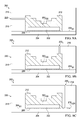
- FIG. 8 illustrates a cross-sectional view of an alternative embodiment wave device 200 , which also may be constructed according to method 10 of FIG. 1 , but which results in various different structural aspects. Accordingly, steps relating to method 10 are generally referenced hereinbelow, but their additional details are described hereinabove. Also, various illustrations and descriptions herein use cross-sectional views, which are helpful in understanding the overall device's three dimensions.
- the first step 12 of method 10 attaches a circuit die 202 relative to a first surface 204 S1 of a substrate 204 , where circuit die 202 may include apparatus and functionality for either transmitting or receiving (or both transmitting and receiving) a wave with bandwidth BW D .
- Substrate 204 is constructed of various materials. But with respect to wave device 200 , in contrast to the above-described device 100 , the material of substrate 204 is not required to be transmissive to bandwidth BW D , because the waves are not ultimately transmitted through that structure in this example embodiment. In any event, the attachment of die 202 relative to substrate 204 may include various techniques and structures, where FIG.
- step 14 of method 10 forms a shaped sublimatable material relative to a region of circuit die 202 , and a sublimatable form 212 is created in this example, which is illustrated as having a stair-step profile.
- Form 212 may be created using various processes, including 3-D printing for example, where form 212 provides a precursor shape for forming an adjacent and shape-conforming structure next to the form, as further described hereinbelow.
- FIG. 1 steps 16 and 18 are combined with respect to a single structure. More particularly, a conforming wave shaping member 218 (or plural members) is/are formed adjacent the sublimatable form 212 .
- conforming wave shaping member 218 (step 16 of method 10 ) is an integrated circuit packaging material (step 18 of method 10 ) applied over the device, preferably so as to encapsulate the sublimatable form 212 and the remainder of the items affixed to substrate 204 .
- FIG. 9A illustrates the cross-sectional view of FIG.
- the molding materials(s) forming member 218 are selected with a consideration of the type and/or bandwidth BW D of the wave that is communicated relative to device 100 , so that such materials readily permit the wave to transmit through member 218 with little or no change in the signal strength, so the molding material does not have strong absorbance in the bandwidth BW D of interest.
- a lateral aperture 220 is also created in fluid (e.g., air) communication with the sublimatable form 212 .
- FIG. 10 illustrates the cross-sectional view from FIG. 9A , further demonstrating step 20 of method 10 as applied to device 200 .
- FIG. 10 depicts that sublimatable form 212 from FIG. 9A is sublimated, again by process(es) to transition the substance directly from the solid to the gas phase without passing through the intermediate liquid phase.
- the sublimatable material encapsulated by encapsulating mold 218 turns to gas and is exhausted via aperture 220 , as shown by dotted arrows in the Figure. Therefore, in a resulting device 200 , an interior cavity remains relative to the surface of circuit die 212 , and waves may propagate with little or no interference from the air in that cavity.
- FIG. 11 illustrates the cross-sectional view from FIG. 10 , further demonstrating steps 22 and 24 of method 10 , as applied to device 200 .
- a cover 222 may be formed over the aperture 220 that was formerly in the packaging material, as shown in FIG. 10 .
- cover 222 encloses any open cavity between encapsulating mold 218 and circuit die 202 .
- FIG. 11 shows the final step 24 from FIG. 1 to process waves.
- Mold 218 comprises materials that readily permit the wave to transmit through it, with little or no change in the signal direction or strength. As a result, FIG. 11 shows such waves directed toward, and passing through, mold 218 .
- mold 218 presents a surface facing circuit die 202 and thereby creates a refractive directionality of the waves, so as to focus or direct the waves more toward the communication surface 202 CS of die 202 .
- mold 218 either alone or in combination with the air interface from the cavity left behind after sublimation of form 212 , again provides wave shaping directionality of the waves toward circuit die 202 (or, in an alternative embodiment, die 202 includes a transmitter, and such directionality may be achieved away from circuit die 202 ).
- mold 218 provides a lens, so as to change the direction of waves impinging on a first surface of the lens relative to the waves as they depart from a second surface of the lens.
- devices 200 1 and 200 2 both include vertical apertures 220 1 and 200 2 , respectively, as may be implemented in connection with both conventional molding processes and the above-described film assist molding approach.
- vertical aperture 220 1 is positioned toward a far (e.g., right, as shown) vertical edge of sublimatable form 212 , so as to serve the exhausting function described hereinabove, while still permitting a vertical implementation of the aperture through the integrated circuit packaging material wave shaping member 218 .
- This positioning is desirable, because it reduces the effect (if any) that the remaining bore of the aperture could have on disturbing the path of waves to/from device 200 1 .
- FIG. 9C illustrates for device 200 2 that form 212 includes a lateral extension 212 LEX , so as to provide a path for aperture 220 2 to be positioned even a greater distance laterally relative to communication surface 202 CS .
- various example embodiments provide improvements to: a method of creating; and a resulting integrated circuit wave device that communicates waves with a bandwidth that is minimally affected as the waves pass through an external portion of the device and are shaped internally of the device, either to or from an encapsulated integrated circuit die.
- Example embodiments may be created for waves of various bandwidths, with radio frequency (RF), visible light and infrared (IR) communication elements.
- RF radio frequency
- IR infrared
- Directionality and/or focus also may be used to a central point or to multiple points, such as with an array of sensors or transmitters.
- Such internal wave shaping is achieved by creating a form and an adjacent shape, where the form: is thereafter sublimated, leaving behind an air cavity and a wave shaping member; or is of a material that has at most a negligible effect on the bandwidth BW D of the waves passing through it.
- the wave shaping member may have many forms, such as lenses (e.g., Fresnel) or reflector shapes, where the shaping device may include singular or multiple such devices.
- different example embodiments may be created for different respective bandwidths BW D , and the device may thereby provide (or be incorporated into) numerous apparatus or applications, such as photodetctors/photosensors, cameras, range finders, focusing devices, targeting systems, automotive detectors and numerous others.
Landscapes
- Physics & Mathematics (AREA)
- General Physics & Mathematics (AREA)
- Optics & Photonics (AREA)
- Engineering & Computer Science (AREA)
- Microelectronics & Electronic Packaging (AREA)
- Condensed Matter Physics & Semiconductors (AREA)
- Computer Hardware Design (AREA)
- Power Engineering (AREA)
- Manufacturing & Machinery (AREA)
- Structures Or Materials For Encapsulating Or Coating Semiconductor Devices Or Solid State Devices (AREA)
Abstract
Description
Claims (22)
Priority Applications (1)
| Application Number | Priority Date | Filing Date | Title |
|---|---|---|---|
| US15/913,497 US10424551B2 (en) | 2016-12-30 | 2018-03-06 | Integrated circuit wave device and method |
Applications Claiming Priority (2)
| Application Number | Priority Date | Filing Date | Title |
|---|---|---|---|
| US15/395,456 US9929110B1 (en) | 2016-12-30 | 2016-12-30 | Integrated circuit wave device and method |
| US15/913,497 US10424551B2 (en) | 2016-12-30 | 2018-03-06 | Integrated circuit wave device and method |
Related Parent Applications (1)
| Application Number | Title | Priority Date | Filing Date |
|---|---|---|---|
| US15/395,456 Continuation US9929110B1 (en) | 2016-12-30 | 2016-12-30 | Integrated circuit wave device and method |
Publications (2)
| Publication Number | Publication Date |
|---|---|
| US20180197830A1 US20180197830A1 (en) | 2018-07-12 |
| US10424551B2 true US10424551B2 (en) | 2019-09-24 |
Family
ID=61629757
Family Applications (2)
| Application Number | Title | Priority Date | Filing Date |
|---|---|---|---|
| US15/395,456 Active US9929110B1 (en) | 2016-12-30 | 2016-12-30 | Integrated circuit wave device and method |
| US15/913,497 Active US10424551B2 (en) | 2016-12-30 | 2018-03-06 | Integrated circuit wave device and method |
Family Applications Before (1)
| Application Number | Title | Priority Date | Filing Date |
|---|---|---|---|
| US15/395,456 Active US9929110B1 (en) | 2016-12-30 | 2016-12-30 | Integrated circuit wave device and method |
Country Status (1)
| Country | Link |
|---|---|
| US (2) | US9929110B1 (en) |
Families Citing this family (9)
| Publication number | Priority date | Publication date | Assignee | Title |
|---|---|---|---|---|
| US11211305B2 (en) | 2016-04-01 | 2021-12-28 | Texas Instruments Incorporated | Apparatus and method to support thermal management of semiconductor-based components |
| US10861796B2 (en) | 2016-05-10 | 2020-12-08 | Texas Instruments Incorporated | Floating die package |
| US10179730B2 (en) | 2016-12-08 | 2019-01-15 | Texas Instruments Incorporated | Electronic sensors with sensor die in package structure cavity |
| US10411150B2 (en) | 2016-12-30 | 2019-09-10 | Texas Instruments Incorporated | Optical isolation systems and circuits and photon detectors with extended lateral P-N junctions |
| US10074639B2 (en) | 2016-12-30 | 2018-09-11 | Texas Instruments Incorporated | Isolator integrated circuits with package structure cavity and fabrication methods |
| US9929110B1 (en) * | 2016-12-30 | 2018-03-27 | Texas Instruments Incorporated | Integrated circuit wave device and method |
| US10121847B2 (en) | 2017-03-17 | 2018-11-06 | Texas Instruments Incorporated | Galvanic isolation device |
| CN109681793B (en) * | 2018-02-02 | 2019-12-27 | 全亿大科技(佛山)有限公司 | Lens, light guide cover and double-sided light emitting device |
| US11935844B2 (en) * | 2020-12-31 | 2024-03-19 | Texas Instruments Incorporated | Semiconductor device and method of the same |
Citations (88)
| Publication number | Priority date | Publication date | Assignee | Title |
|---|---|---|---|---|
| US3508126A (en) | 1964-08-19 | 1970-04-21 | Philips Corp | Semiconductor photodiode with p-n junction spaced from heterojunction |
| US3952265A (en) | 1974-10-29 | 1976-04-20 | Hughes Aircraft Company | Monolithic dual mode emitter-detector terminal for optical waveguide transmission lines |
| US4007978A (en) | 1974-01-18 | 1977-02-15 | Texas Instruments Incorporated | Integrated optical circuits |
| US4267484A (en) | 1979-08-28 | 1981-05-12 | The United States Of America As Represented By The Secretary Of The Air Force | Parallel multi-electrode spark gap switch |
| US4272753A (en) | 1978-08-16 | 1981-06-09 | Harris Corporation | Integrated circuit fuse |
| US4891730A (en) | 1989-05-10 | 1990-01-02 | The United States Of America As Represented By The Secretary Of The Army | Monolithic microwave integrated circuit terminal protection device |
| US4916506A (en) | 1988-11-18 | 1990-04-10 | Sprague Electric Company | Integrated-circuit lead-frame package with low-resistance ground-lead and heat-sink means |
| US4996577A (en) | 1984-01-23 | 1991-02-26 | International Rectifier Corporation | Photovoltaic isolator and process of manufacture thereof |
| US5340993A (en) | 1993-04-30 | 1994-08-23 | Motorola, Inc. | Optocoupler package wth integral voltage isolation barrier |
| US5389578A (en) | 1994-01-04 | 1995-02-14 | Texas Instruments Incorporated | Optical coupler |
| US5514892A (en) | 1994-09-30 | 1996-05-07 | Motorola, Inc. | Electrostatic discharge protection device |
| US5629838A (en) | 1993-06-24 | 1997-05-13 | Polychip, Inc. | Apparatus for non-conductively interconnecting integrated circuits using half capacitors |
| US5796570A (en) | 1996-09-19 | 1998-08-18 | National Semiconductor Corporation | Electrostatic discharge protection package |
| US5929514A (en) | 1998-05-26 | 1999-07-27 | Analog Devices, Inc. | Thermally enhanced lead-under-paddle I.C. leadframe |
| US5990519A (en) | 1998-11-27 | 1999-11-23 | United Microelectronics Corp. | Electrostatic discharge structure |
| US6031251A (en) | 1993-06-07 | 2000-02-29 | Motorola, Inc. | Linear integrated optocoupler and method for forming the same |
| US6242987B1 (en) | 1998-01-08 | 2001-06-05 | Infineon Technologies Ag | Oscillator structure having resonator disposed below oscillator circuit |
| RU2169962C2 (en) | 1999-07-13 | 2001-06-27 | Минг-Тунг ШЕН | Module with semiconductor integrated circuits and its manufacturing process |
| US6351011B1 (en) | 1998-12-08 | 2002-02-26 | Littlefuse, Inc. | Protection of an integrated circuit with voltage variable materials |
| US6365433B1 (en) | 1999-04-27 | 2002-04-02 | Sanyo Electric Co., Ltd. | Semiconductor device and manufacturing method thereof |
| US6507264B1 (en) | 2000-08-28 | 2003-01-14 | Littelfuse, Inc. | Integral fuse for use in semiconductor packages |
| US6509574B2 (en) | 1999-12-02 | 2003-01-21 | Texas Instruments Incorporated | Optocouplers having integrated organic light-emitting diodes |
| RU2201017C2 (en) | 2000-10-26 | 2003-03-20 | Зао "Синтэк" | Optron |
| US20030183916A1 (en) | 2002-03-27 | 2003-10-02 | John Heck | Packaging microelectromechanical systems |
| US20030222205A1 (en) | 2002-03-26 | 2003-12-04 | Hiroyuki Shoji | Photocoupler, method for producing the same, and electronic device equipped with the photocoupler |
| US20040080025A1 (en) | 2002-09-17 | 2004-04-29 | Shinko Electric Industries Co., Ltd. | Lead frame, method of manufacturing the same, and semiconductor device manufactured with the same |
| US20040084729A1 (en) | 2002-11-05 | 2004-05-06 | Leung Ka Y. | High voltage difference amplifier with spark gap ESD protection |
| US20040111881A1 (en) | 2002-01-23 | 2004-06-17 | Hung Yu Yang | Method of manufacturing an on-chip transformer balun |
| US6815808B2 (en) | 2000-10-10 | 2004-11-09 | Sanyo Electric, Co., Ltd. | Hollow airtight semiconductor device package |
| US6821822B1 (en) | 1998-03-26 | 2004-11-23 | Seiko Epson Corporation | Method of manufacturing semiconductor device, molding device for semiconductor device, and semiconductor device |
| US20050218300A1 (en) | 2004-04-02 | 2005-10-06 | Quinones Maria Clemens Y | Surface mount multi-channel optocoupler |
| RU2263999C1 (en) | 2004-02-02 | 2005-11-10 | ЗАО "Синтез электронных компонентов" | Integrated optocoupler |
| US6977468B1 (en) | 2003-02-03 | 2005-12-20 | Auburn University | Integrated spark gap device |
| US7015587B1 (en) | 2004-09-07 | 2006-03-21 | National Semiconductor Corporation | Stacked die package for semiconductor devices |
| US20060205106A1 (en) | 2005-02-25 | 2006-09-14 | Hiroshi Fukuda | Integrated micro electro-mechanical system and manufacturing method thereof |
| US20060281334A1 (en) | 2005-05-12 | 2006-12-14 | Lg Chem, Ltd. | Method for forming high-resolution pattern and substrate having prepattern formed thereby |
| US20070076421A1 (en) | 2005-10-05 | 2007-04-05 | Honda Motor Co., Ltd. | Turn signal lamp for a vehicle |
| US20070152308A1 (en) | 2004-10-18 | 2007-07-05 | Chippac, Inc | Multichip leadframe package |
| US20070229177A1 (en) | 2006-03-17 | 2007-10-04 | Kouichi Moriya | Surface mount crystal oscillator |
| US7321162B1 (en) | 1999-10-15 | 2008-01-22 | Amkor Technology, Inc. | Semiconductor package having reduced thickness |
| US7334326B1 (en) | 2001-06-19 | 2008-02-26 | Amkor Technology, Inc. | Method for making an integrated circuit substrate having embedded passive components |
| US20080217759A1 (en) | 2007-03-06 | 2008-09-11 | Taiwan Solutions Systems Corp. | Chip package substrate and structure thereof |
| EP1986297A2 (en) | 2007-04-25 | 2008-10-29 | MediaTek Inc. | Spark gaps for ESD protection |
| US20090052214A1 (en) | 2007-08-13 | 2009-02-26 | Fuji Electric Device Technology Co., Ltd. | Insulating transformer and power conversion device |
| US20090115049A1 (en) | 2007-11-06 | 2009-05-07 | Shinko Electric Industries Co., Ltd. | Semiconductor package |
| US20090127638A1 (en) | 2007-11-16 | 2009-05-21 | Infineon Technologies Ag | Electrical device and method |
| US7732892B2 (en) | 2006-11-03 | 2010-06-08 | Taiwan Semiconductor Manufacturing Co., Ltd. | Fuse structures and integrated circuit devices |
| US20100187652A1 (en) | 2008-07-28 | 2010-07-29 | Yang Xiao Charles | Method and structures of monolithically integrated esd suppression device |
| US20100252923A1 (en) | 2009-04-07 | 2010-10-07 | Elpida Memory, Inc. | Semiconductor device and method of manufacturing same |
| US7842542B2 (en) | 2008-07-14 | 2010-11-30 | Stats Chippac, Ltd. | Embedded semiconductor die package and method of making the same using metal frame carrier |
| US7869180B2 (en) | 2004-06-30 | 2011-01-11 | Research In Motion Limited | Spark gap apparatus and method for electrostatic discharge protection |
| US20110089540A1 (en) | 2009-10-16 | 2011-04-21 | Sun Microsystems, Inc. | Semiconductor die with integrated electro-static discharge device |
| US20110108747A1 (en) | 2009-11-12 | 2011-05-12 | Yong Liu | Optocoupler devices |
| US8018705B2 (en) | 2005-09-14 | 2011-09-13 | University Of Witwatersrand | Spark gap protection device |
| US20110233790A1 (en) | 2010-03-25 | 2011-09-29 | Qualcomm Incorporated | Sacrificial Material to Facilitate Thin Die Attach |
| EP2490263A2 (en) | 2011-02-17 | 2012-08-22 | Nxp B.V. | Optocoupler circuit |
| US8433084B2 (en) | 2009-05-11 | 2013-04-30 | Stmicroelectronics S.R.L. | Assembly of a capacitive acoustic transducer of the microelectromechanical type and package thereof |
| US8436460B1 (en) | 2007-05-04 | 2013-05-07 | Cypress Semiconductor Corporation | Multiple die paddle leadframe and semiconductor device package |
| US20130134445A1 (en) | 2011-11-29 | 2013-05-30 | Cree, Inc. | Complex primary optics and methods of fabrication |
| US20130194057A1 (en) | 2012-01-30 | 2013-08-01 | Avago Technologies Wireless Ip (Singapore) Pte. Ltd. | Temperature controlled acoustic resonator |
| US8569082B2 (en) | 2008-10-14 | 2013-10-29 | Texas Instruments Incorporated | Semiconductor package with a mold material encapsulating a chip and a portion of a lead frame |
| US20130315533A1 (en) | 2012-05-23 | 2013-11-28 | Avago Technologies Ecbu Ip (Singapore) Pte. Ltd. | Premolded cavity for optoelectronic device |
| US20130320548A1 (en) | 2012-05-31 | 2013-12-05 | Burton J. Carpenter | Integrated circuit die assembly with heat spreader |
| US20130329324A1 (en) | 2012-06-09 | 2013-12-12 | Apple Inc. | Esd path for connector receptacle |
| US20140001632A1 (en) | 2012-06-29 | 2014-01-02 | Trent S. Uehling | Semiconductor package structure having an air gap and method for forming |
| US8633551B1 (en) | 2012-06-29 | 2014-01-21 | Intel Corporation | Semiconductor package with mechanical fuse |
| US20140091909A1 (en) | 2012-10-01 | 2014-04-03 | Patrick Smith | Surveillance Devices with Multiple Capacitors |
| US20140264905A1 (en) | 2013-03-13 | 2014-09-18 | Stats Chippac, Ltd. | Semiconductor Device and Method of Forming WLCSP with Semiconductor Die Embedded within Interconnect Structure |
| US20150035091A1 (en) | 2013-07-31 | 2015-02-05 | Stmicroelectronics S.R.I. | Process for manufacturing a packaged device, in particular a packaged micro-electro-mechanical sensor, having an accessible structure, such as a mems microphone and packaged device obtained thereby |
| US20150069537A1 (en) | 2013-09-08 | 2015-03-12 | Wai Yew Lo | Package-on-package semiconductor sensor device |
| GB2521619A (en) | 2013-12-23 | 2015-07-01 | Nokia Technologies Oy | An apparatus and associated methods for flexible carrier substrates |
| US20150249043A1 (en) | 2014-02-28 | 2015-09-03 | Infineon Technologies Ag | Method of Packaging a Semiconductor Chip Using a 3D Printing Process and Semiconductor Package Having Angled Surfaces |
| US20150255693A1 (en) | 2012-05-24 | 2015-09-10 | Osram Opto Semiconductors Gmbh | Optoelectronic component device and method for producing an optoelectronic component device |
| US9184012B2 (en) | 2012-12-19 | 2015-11-10 | Allegro Microsystems, Llc | Integrated circuit fuse and method of fabricating the integrated circuit fuse |
| US20150369682A1 (en) | 2014-06-18 | 2015-12-24 | Seiko Epson Corporation | Physical Quantity Sensor Apparatus, Altimeter, Electronic Apparatus, And Moving Object |
| US20150369681A1 (en) | 2014-06-18 | 2015-12-24 | Seiko Epson Corporation | Physical quantity sensor, electronic device, altimeter, electronic apparatus, and mobile object |
| US20150380353A1 (en) | 2013-02-12 | 2015-12-31 | Freescale Semiconductor, Inc. | Method of fabricating an integrated circuit device, and an integrated circuit device therefrom |
| US20160003436A1 (en) | 2013-02-08 | 2016-01-07 | Osram Opto Semiconductors Gmbh | Optoelectronic Lighting Module, Optoelectronic Lighting Apparatus and Vehicle Headlamp |
| US20160064696A1 (en) | 2014-08-27 | 2016-03-03 | 3M Innovative Properties Company | Thermally-assisted self-assembly method of nanoparticles and nanowires within engineered periodic structures |
| US20160103082A1 (en) | 2013-05-23 | 2016-04-14 | Mitsuteru Kimura | Hydrogen gas sensor with concentration function and hydrogen gas sensor probe used in same |
| US20160167089A1 (en) | 2014-12-11 | 2016-06-16 | Palo Alto Research Center Incorporation | Forming sacrificial structures using phase-change materials that sublimate |
| US20160209285A1 (en) | 2015-01-20 | 2016-07-21 | Seiko Epson Corporation | Pressure sensor, method of manufacturing pressure sensor, altimeter, electronic apparatus, and moving object |
| US9419075B1 (en) | 2015-01-28 | 2016-08-16 | Texas Instruments Incorporated | Wafer substrate removal |
| US20170089789A1 (en) | 2015-09-28 | 2017-03-30 | Seiko Epson Corporation | Pressure sensor, altimeter, electronic apparatus, and moving object |
| US20170134004A1 (en) | 2015-11-10 | 2017-05-11 | Seiko Epson Corporation | Oscillator, electronic apparatus, and moving object |
| US9748207B2 (en) | 2014-06-23 | 2017-08-29 | The Silanna Group Pty Ltd | Bonded dies with isolation |
| US20170330841A1 (en) | 2016-05-10 | 2017-11-16 | Texas Instruments Incorporated | Floating Die Package |
| US9929110B1 (en) * | 2016-12-30 | 2018-03-27 | Texas Instruments Incorporated | Integrated circuit wave device and method |
-
2016
- 2016-12-30 US US15/395,456 patent/US9929110B1/en active Active
-
2018
- 2018-03-06 US US15/913,497 patent/US10424551B2/en active Active
Patent Citations (89)
| Publication number | Priority date | Publication date | Assignee | Title |
|---|---|---|---|---|
| US3508126A (en) | 1964-08-19 | 1970-04-21 | Philips Corp | Semiconductor photodiode with p-n junction spaced from heterojunction |
| US4007978A (en) | 1974-01-18 | 1977-02-15 | Texas Instruments Incorporated | Integrated optical circuits |
| US3952265A (en) | 1974-10-29 | 1976-04-20 | Hughes Aircraft Company | Monolithic dual mode emitter-detector terminal for optical waveguide transmission lines |
| US4272753A (en) | 1978-08-16 | 1981-06-09 | Harris Corporation | Integrated circuit fuse |
| US4267484A (en) | 1979-08-28 | 1981-05-12 | The United States Of America As Represented By The Secretary Of The Air Force | Parallel multi-electrode spark gap switch |
| US4996577A (en) | 1984-01-23 | 1991-02-26 | International Rectifier Corporation | Photovoltaic isolator and process of manufacture thereof |
| US4916506A (en) | 1988-11-18 | 1990-04-10 | Sprague Electric Company | Integrated-circuit lead-frame package with low-resistance ground-lead and heat-sink means |
| US4891730A (en) | 1989-05-10 | 1990-01-02 | The United States Of America As Represented By The Secretary Of The Army | Monolithic microwave integrated circuit terminal protection device |
| US5340993A (en) | 1993-04-30 | 1994-08-23 | Motorola, Inc. | Optocoupler package wth integral voltage isolation barrier |
| US6031251A (en) | 1993-06-07 | 2000-02-29 | Motorola, Inc. | Linear integrated optocoupler and method for forming the same |
| US5629838A (en) | 1993-06-24 | 1997-05-13 | Polychip, Inc. | Apparatus for non-conductively interconnecting integrated circuits using half capacitors |
| US5389578A (en) | 1994-01-04 | 1995-02-14 | Texas Instruments Incorporated | Optical coupler |
| US5514892A (en) | 1994-09-30 | 1996-05-07 | Motorola, Inc. | Electrostatic discharge protection device |
| US5796570A (en) | 1996-09-19 | 1998-08-18 | National Semiconductor Corporation | Electrostatic discharge protection package |
| US6242987B1 (en) | 1998-01-08 | 2001-06-05 | Infineon Technologies Ag | Oscillator structure having resonator disposed below oscillator circuit |
| US6821822B1 (en) | 1998-03-26 | 2004-11-23 | Seiko Epson Corporation | Method of manufacturing semiconductor device, molding device for semiconductor device, and semiconductor device |
| US5929514A (en) | 1998-05-26 | 1999-07-27 | Analog Devices, Inc. | Thermally enhanced lead-under-paddle I.C. leadframe |
| US5990519A (en) | 1998-11-27 | 1999-11-23 | United Microelectronics Corp. | Electrostatic discharge structure |
| US6351011B1 (en) | 1998-12-08 | 2002-02-26 | Littlefuse, Inc. | Protection of an integrated circuit with voltage variable materials |
| US6365433B1 (en) | 1999-04-27 | 2002-04-02 | Sanyo Electric Co., Ltd. | Semiconductor device and manufacturing method thereof |
| RU2169962C2 (en) | 1999-07-13 | 2001-06-27 | Минг-Тунг ШЕН | Module with semiconductor integrated circuits and its manufacturing process |
| US7321162B1 (en) | 1999-10-15 | 2008-01-22 | Amkor Technology, Inc. | Semiconductor package having reduced thickness |
| US6509574B2 (en) | 1999-12-02 | 2003-01-21 | Texas Instruments Incorporated | Optocouplers having integrated organic light-emitting diodes |
| US6507264B1 (en) | 2000-08-28 | 2003-01-14 | Littelfuse, Inc. | Integral fuse for use in semiconductor packages |
| US6815808B2 (en) | 2000-10-10 | 2004-11-09 | Sanyo Electric, Co., Ltd. | Hollow airtight semiconductor device package |
| RU2201017C2 (en) | 2000-10-26 | 2003-03-20 | Зао "Синтэк" | Optron |
| US7334326B1 (en) | 2001-06-19 | 2008-02-26 | Amkor Technology, Inc. | Method for making an integrated circuit substrate having embedded passive components |
| US20040111881A1 (en) | 2002-01-23 | 2004-06-17 | Hung Yu Yang | Method of manufacturing an on-chip transformer balun |
| US20030222205A1 (en) | 2002-03-26 | 2003-12-04 | Hiroyuki Shoji | Photocoupler, method for producing the same, and electronic device equipped with the photocoupler |
| US20030183916A1 (en) | 2002-03-27 | 2003-10-02 | John Heck | Packaging microelectromechanical systems |
| US20040080025A1 (en) | 2002-09-17 | 2004-04-29 | Shinko Electric Industries Co., Ltd. | Lead frame, method of manufacturing the same, and semiconductor device manufactured with the same |
| US20040084729A1 (en) | 2002-11-05 | 2004-05-06 | Leung Ka Y. | High voltage difference amplifier with spark gap ESD protection |
| US6977468B1 (en) | 2003-02-03 | 2005-12-20 | Auburn University | Integrated spark gap device |
| RU2263999C1 (en) | 2004-02-02 | 2005-11-10 | ЗАО "Синтез электронных компонентов" | Integrated optocoupler |
| US20050218300A1 (en) | 2004-04-02 | 2005-10-06 | Quinones Maria Clemens Y | Surface mount multi-channel optocoupler |
| US7869180B2 (en) | 2004-06-30 | 2011-01-11 | Research In Motion Limited | Spark gap apparatus and method for electrostatic discharge protection |
| US7015587B1 (en) | 2004-09-07 | 2006-03-21 | National Semiconductor Corporation | Stacked die package for semiconductor devices |
| US20070152308A1 (en) | 2004-10-18 | 2007-07-05 | Chippac, Inc | Multichip leadframe package |
| US20060205106A1 (en) | 2005-02-25 | 2006-09-14 | Hiroshi Fukuda | Integrated micro electro-mechanical system and manufacturing method thereof |
| US20060281334A1 (en) | 2005-05-12 | 2006-12-14 | Lg Chem, Ltd. | Method for forming high-resolution pattern and substrate having prepattern formed thereby |
| US8018705B2 (en) | 2005-09-14 | 2011-09-13 | University Of Witwatersrand | Spark gap protection device |
| US20070076421A1 (en) | 2005-10-05 | 2007-04-05 | Honda Motor Co., Ltd. | Turn signal lamp for a vehicle |
| US20070229177A1 (en) | 2006-03-17 | 2007-10-04 | Kouichi Moriya | Surface mount crystal oscillator |
| US7732892B2 (en) | 2006-11-03 | 2010-06-08 | Taiwan Semiconductor Manufacturing Co., Ltd. | Fuse structures and integrated circuit devices |
| US20080217759A1 (en) | 2007-03-06 | 2008-09-11 | Taiwan Solutions Systems Corp. | Chip package substrate and structure thereof |
| EP1986297A2 (en) | 2007-04-25 | 2008-10-29 | MediaTek Inc. | Spark gaps for ESD protection |
| US20080266730A1 (en) | 2007-04-25 | 2008-10-30 | Karsten Viborg | Spark Gaps for ESD Protection |
| US8436460B1 (en) | 2007-05-04 | 2013-05-07 | Cypress Semiconductor Corporation | Multiple die paddle leadframe and semiconductor device package |
| US20090052214A1 (en) | 2007-08-13 | 2009-02-26 | Fuji Electric Device Technology Co., Ltd. | Insulating transformer and power conversion device |
| US20090115049A1 (en) | 2007-11-06 | 2009-05-07 | Shinko Electric Industries Co., Ltd. | Semiconductor package |
| US20090127638A1 (en) | 2007-11-16 | 2009-05-21 | Infineon Technologies Ag | Electrical device and method |
| US7842542B2 (en) | 2008-07-14 | 2010-11-30 | Stats Chippac, Ltd. | Embedded semiconductor die package and method of making the same using metal frame carrier |
| US20100187652A1 (en) | 2008-07-28 | 2010-07-29 | Yang Xiao Charles | Method and structures of monolithically integrated esd suppression device |
| US8569082B2 (en) | 2008-10-14 | 2013-10-29 | Texas Instruments Incorporated | Semiconductor package with a mold material encapsulating a chip and a portion of a lead frame |
| US20100252923A1 (en) | 2009-04-07 | 2010-10-07 | Elpida Memory, Inc. | Semiconductor device and method of manufacturing same |
| US8433084B2 (en) | 2009-05-11 | 2013-04-30 | Stmicroelectronics S.R.L. | Assembly of a capacitive acoustic transducer of the microelectromechanical type and package thereof |
| US20110089540A1 (en) | 2009-10-16 | 2011-04-21 | Sun Microsystems, Inc. | Semiconductor die with integrated electro-static discharge device |
| US20110108747A1 (en) | 2009-11-12 | 2011-05-12 | Yong Liu | Optocoupler devices |
| US20110233790A1 (en) | 2010-03-25 | 2011-09-29 | Qualcomm Incorporated | Sacrificial Material to Facilitate Thin Die Attach |
| EP2490263A2 (en) | 2011-02-17 | 2012-08-22 | Nxp B.V. | Optocoupler circuit |
| US20130134445A1 (en) | 2011-11-29 | 2013-05-30 | Cree, Inc. | Complex primary optics and methods of fabrication |
| US20130194057A1 (en) | 2012-01-30 | 2013-08-01 | Avago Technologies Wireless Ip (Singapore) Pte. Ltd. | Temperature controlled acoustic resonator |
| US20130315533A1 (en) | 2012-05-23 | 2013-11-28 | Avago Technologies Ecbu Ip (Singapore) Pte. Ltd. | Premolded cavity for optoelectronic device |
| US20150255693A1 (en) | 2012-05-24 | 2015-09-10 | Osram Opto Semiconductors Gmbh | Optoelectronic component device and method for producing an optoelectronic component device |
| US20130320548A1 (en) | 2012-05-31 | 2013-12-05 | Burton J. Carpenter | Integrated circuit die assembly with heat spreader |
| US20130329324A1 (en) | 2012-06-09 | 2013-12-12 | Apple Inc. | Esd path for connector receptacle |
| US20140001632A1 (en) | 2012-06-29 | 2014-01-02 | Trent S. Uehling | Semiconductor package structure having an air gap and method for forming |
| US8633551B1 (en) | 2012-06-29 | 2014-01-21 | Intel Corporation | Semiconductor package with mechanical fuse |
| US20140091909A1 (en) | 2012-10-01 | 2014-04-03 | Patrick Smith | Surveillance Devices with Multiple Capacitors |
| US9184012B2 (en) | 2012-12-19 | 2015-11-10 | Allegro Microsystems, Llc | Integrated circuit fuse and method of fabricating the integrated circuit fuse |
| US20160003436A1 (en) | 2013-02-08 | 2016-01-07 | Osram Opto Semiconductors Gmbh | Optoelectronic Lighting Module, Optoelectronic Lighting Apparatus and Vehicle Headlamp |
| US20150380353A1 (en) | 2013-02-12 | 2015-12-31 | Freescale Semiconductor, Inc. | Method of fabricating an integrated circuit device, and an integrated circuit device therefrom |
| US20140264905A1 (en) | 2013-03-13 | 2014-09-18 | Stats Chippac, Ltd. | Semiconductor Device and Method of Forming WLCSP with Semiconductor Die Embedded within Interconnect Structure |
| US20160103082A1 (en) | 2013-05-23 | 2016-04-14 | Mitsuteru Kimura | Hydrogen gas sensor with concentration function and hydrogen gas sensor probe used in same |
| US20150035091A1 (en) | 2013-07-31 | 2015-02-05 | Stmicroelectronics S.R.I. | Process for manufacturing a packaged device, in particular a packaged micro-electro-mechanical sensor, having an accessible structure, such as a mems microphone and packaged device obtained thereby |
| US20150069537A1 (en) | 2013-09-08 | 2015-03-12 | Wai Yew Lo | Package-on-package semiconductor sensor device |
| GB2521619A (en) | 2013-12-23 | 2015-07-01 | Nokia Technologies Oy | An apparatus and associated methods for flexible carrier substrates |
| US20150249043A1 (en) | 2014-02-28 | 2015-09-03 | Infineon Technologies Ag | Method of Packaging a Semiconductor Chip Using a 3D Printing Process and Semiconductor Package Having Angled Surfaces |
| US20150369681A1 (en) | 2014-06-18 | 2015-12-24 | Seiko Epson Corporation | Physical quantity sensor, electronic device, altimeter, electronic apparatus, and mobile object |
| US20150369682A1 (en) | 2014-06-18 | 2015-12-24 | Seiko Epson Corporation | Physical Quantity Sensor Apparatus, Altimeter, Electronic Apparatus, And Moving Object |
| US9748207B2 (en) | 2014-06-23 | 2017-08-29 | The Silanna Group Pty Ltd | Bonded dies with isolation |
| US20160064696A1 (en) | 2014-08-27 | 2016-03-03 | 3M Innovative Properties Company | Thermally-assisted self-assembly method of nanoparticles and nanowires within engineered periodic structures |
| US20160167089A1 (en) | 2014-12-11 | 2016-06-16 | Palo Alto Research Center Incorporation | Forming sacrificial structures using phase-change materials that sublimate |
| US20160209285A1 (en) | 2015-01-20 | 2016-07-21 | Seiko Epson Corporation | Pressure sensor, method of manufacturing pressure sensor, altimeter, electronic apparatus, and moving object |
| US9419075B1 (en) | 2015-01-28 | 2016-08-16 | Texas Instruments Incorporated | Wafer substrate removal |
| US20170089789A1 (en) | 2015-09-28 | 2017-03-30 | Seiko Epson Corporation | Pressure sensor, altimeter, electronic apparatus, and moving object |
| US20170134004A1 (en) | 2015-11-10 | 2017-05-11 | Seiko Epson Corporation | Oscillator, electronic apparatus, and moving object |
| US20170330841A1 (en) | 2016-05-10 | 2017-11-16 | Texas Instruments Incorporated | Floating Die Package |
| US9929110B1 (en) * | 2016-12-30 | 2018-03-27 | Texas Instruments Incorporated | Integrated circuit wave device and method |
Non-Patent Citations (12)
| Title |
|---|
| Cameron G. Clark, "The Basics of Arc Flash," GE Industrial Solutions web site accessed Oct. 5, 2016, http://apps.geindustrial.com/publibrary/checkout/ArcFlash4?TNR=White%20Papers%7CArcFlash4%7Cgeneric (3 pages). |
| European Search Report for 17796774.2 dated May 9, 2019. |
| International Search Report for PCT/US2017/031987 dated Sep. 7, 2017. |
| International Search Report for PCT/US2017/068983 dated May 17, 2018. |
| International Search Report for PCT/US2017/068997 dated May 24, 2018. |
| Maloberti, F., "Layout of Analog CMOS Integrated Circuit, Part 2 Transistors and Basic Cells Layout," retrieved from http://ims.unipv.it/Courses/download/AIC/Layout02.pdf, dated Mar. 15, 2004 (38 pages). |
| National Semiconductor Corporation, "Semiconductor Packaging Assembly Technology," National Semiconductor Corporation, Aug. 1999, pp. 1-8. |
| OSRAM Opto Semiconductors GmbH, Oslon Compact (850nm), version 1.6; SFH 4710; dated Dec. 1, 2015; 13 pages. |
| Texas Instruments Application Report "The ISO72x Family of High-Speed Digital Isolators," SLLA198—Jan. 2006 (12 pages). |
| Texas Instruments Developers Guide "Digital Isolator Design Guide," SLLA284A, Jan. 2009 (19 pages). |
| Texas Instruments Product Brochure ISO7841x High-Performance, 8000-Vpk Reinforced Quad-Channel Digital Isolator, dated Nov. 2014 (37 pages). |
| Wikipedia article "3D Printing," retrieved from "http://en.wikipedia.org/w/index.php?title=3D_printing&oldid=624190184", dated Sep. 4, 2014 (35 pages). |
Also Published As
| Publication number | Publication date |
|---|---|
| US20180197830A1 (en) | 2018-07-12 |
| US9929110B1 (en) | 2018-03-27 |
Similar Documents
| Publication | Publication Date | Title |
|---|---|---|
| US10424551B2 (en) | Integrated circuit wave device and method | |
| KR102459731B1 (en) | Optical Fingerprint Sensor Package | |
| CN103119925B (en) | Infrared camera architecture system and method | |
| US8114304B2 (en) | Method for producing electronic components | |
| JP5362003B2 (en) | Mold optical package with fiber coupling | |
| EP2828629B1 (en) | Electromagnetic radiation micro device, wafer element and method for manufacturing such a micro device | |
| US20040201090A1 (en) | Electronic device with cavity and a method for producing the same | |
| US20050014307A1 (en) | Manufacturing method of a semiconductor device | |
| JP7660061B2 (en) | Semiconductor package, electronic device, and method for manufacturing semiconductor package | |
| US9742968B2 (en) | Image acquisition system and method for the manufacture thereof | |
| CN114361151A (en) | Novel optical sensing chip packaging structure combined with super lens | |
| KR20070041572A (en) | How to manufacture a camera module at the wafer level | |
| CN110556368A (en) | Photoelectric sensor and preparation method thereof | |
| JP4335851B2 (en) | Gas sensor module for spectroscopically measuring gas concentration | |
| CN114325641A (en) | Photoinduction chip and manufacturing method thereof, laser radar and electronic equipment | |
| US20100096717A1 (en) | Electronic device and process for manufacturing electronic device | |
| CN115015948A (en) | Optical sensor and manufacturing method | |
| CN100446248C (en) | Electronic component and its manufacturing method | |
| US10529869B2 (en) | Electronic component, electronic equipment, and method for manufacturing electronic component | |
| US11894339B2 (en) | Proximity sensor | |
| WO2009137022A1 (en) | Camera system including radiation shield and method of shielding radiation | |
| CN101567321A (en) | Packaging method of image sensing device | |
| JP2010243365A (en) | Infrared sensor device manufacturing method | |
| JP7055010B2 (en) | Optical equipment | |
| WO2014027476A1 (en) | Semiconductor device |
Legal Events
| Date | Code | Title | Description |
|---|---|---|---|
| FEPP | Fee payment procedure |
Free format text: ENTITY STATUS SET TO UNDISCOUNTED (ORIGINAL EVENT CODE: BIG.); ENTITY STATUS OF PATENT OWNER: LARGE ENTITY |
|
| STPP | Information on status: patent application and granting procedure in general |
Free format text: FINAL REJECTION MAILED |
|
| STPP | Information on status: patent application and granting procedure in general |
Free format text: NOTICE OF ALLOWANCE MAILED -- APPLICATION RECEIVED IN OFFICE OF PUBLICATIONS |
|
| STPP | Information on status: patent application and granting procedure in general |
Free format text: AWAITING TC RESP, ISSUE FEE PAYMENT RECEIVED |
|
| STPP | Information on status: patent application and granting procedure in general |
Free format text: PUBLICATIONS -- ISSUE FEE PAYMENT VERIFIED |
|
| STCF | Information on status: patent grant |
Free format text: PATENTED CASE |
|
| MAFP | Maintenance fee payment |
Free format text: PAYMENT OF MAINTENANCE FEE, 4TH YEAR, LARGE ENTITY (ORIGINAL EVENT CODE: M1551); ENTITY STATUS OF PATENT OWNER: LARGE ENTITY Year of fee payment: 4 |