US10381473B2 - High-electron-mobility transistor with buried interconnect - Google Patents
High-electron-mobility transistor with buried interconnect Download PDFInfo
- Publication number
- US10381473B2 US10381473B2 US15/643,328 US201715643328A US10381473B2 US 10381473 B2 US10381473 B2 US 10381473B2 US 201715643328 A US201715643328 A US 201715643328A US 10381473 B2 US10381473 B2 US 10381473B2
- Authority
- US
- United States
- Prior art keywords
- layer
- contact
- disposed
- trench
- electronic device
- Prior art date
- Legal status (The legal status is an assumption and is not a legal conclusion. Google has not performed a legal analysis and makes no representation as to the accuracy of the status listed.)
- Active
Links
Images


Classifications
-
- H01L29/7787—
-
- H—ELECTRICITY
- H10—SEMICONDUCTOR DEVICES; ELECTRIC SOLID-STATE DEVICES NOT OTHERWISE PROVIDED FOR
- H10D—INORGANIC ELECTRIC SEMICONDUCTOR DEVICES
- H10D30/00—Field-effect transistors [FET]
- H10D30/40—FETs having zero-dimensional [0D], one-dimensional [1D] or two-dimensional [2D] charge carrier gas channels
- H10D30/47—FETs having zero-dimensional [0D], one-dimensional [1D] or two-dimensional [2D] charge carrier gas channels having 2D charge carrier gas channels, e.g. nanoribbon FETs or high electron mobility transistors [HEMT]
- H10D30/471—High electron mobility transistors [HEMT] or high hole mobility transistors [HHMT]
- H10D30/475—High electron mobility transistors [HEMT] or high hole mobility transistors [HHMT] having wider bandgap layer formed on top of lower bandgap active layer, e.g. undoped barrier HEMTs such as i-AlGaN/GaN HEMTs
- H10D30/4755—High electron mobility transistors [HEMT] or high hole mobility transistors [HHMT] having wider bandgap layer formed on top of lower bandgap active layer, e.g. undoped barrier HEMTs such as i-AlGaN/GaN HEMTs having wide bandgap charge-carrier supplying layers, e.g. modulation doped HEMTs such as n-AlGaAs/GaAs HEMTs
-
- H10W20/031—
-
- H—ELECTRICITY
- H01—ELECTRIC ELEMENTS
- H01L—SEMICONDUCTOR DEVICES NOT COVERED BY CLASS H10
- H01L21/00—Processes or apparatus adapted for the manufacture or treatment of semiconductor or solid state devices or of parts thereof
- H01L21/02—Manufacture or treatment of semiconductor devices or of parts thereof
- H01L21/02104—Forming layers
- H01L21/02365—Forming inorganic semiconducting materials on a substrate
- H01L21/02367—Substrates
- H01L21/0237—Materials
- H01L21/02373—Group 14 semiconducting materials
- H01L21/02381—Silicon, silicon germanium, germanium
-
- H—ELECTRICITY
- H01—ELECTRIC ELEMENTS
- H01L—SEMICONDUCTOR DEVICES NOT COVERED BY CLASS H10
- H01L21/00—Processes or apparatus adapted for the manufacture or treatment of semiconductor or solid state devices or of parts thereof
- H01L21/02—Manufacture or treatment of semiconductor devices or of parts thereof
- H01L21/02104—Forming layers
- H01L21/02365—Forming inorganic semiconducting materials on a substrate
- H01L21/02518—Deposited layers
- H01L21/02521—Materials
- H01L21/02538—Group 13/15 materials
- H01L21/0254—Nitrides
-
- H—ELECTRICITY
- H01—ELECTRIC ELEMENTS
- H01L—SEMICONDUCTOR DEVICES NOT COVERED BY CLASS H10
- H01L21/00—Processes or apparatus adapted for the manufacture or treatment of semiconductor or solid state devices or of parts thereof
- H01L21/70—Manufacture or treatment of devices consisting of a plurality of solid state components formed in or on a common substrate or of parts thereof; Manufacture of integrated circuit devices or of parts thereof
- H01L21/71—Manufacture of specific parts of devices defined in group H01L21/70
- H01L21/768—Applying interconnections to be used for carrying current between separate components within a device comprising conductors and dielectrics
- H01L21/76838—Applying interconnections to be used for carrying current between separate components within a device comprising conductors and dielectrics characterised by the formation and the after-treatment of the conductors
- H01L21/76895—Local interconnects; Local pads, as exemplified by patent document EP0896365
-
- H—ELECTRICITY
- H01—ELECTRIC ELEMENTS
- H01L—SEMICONDUCTOR DEVICES NOT COVERED BY CLASS H10
- H01L23/00—Details of semiconductor or other solid state devices
- H01L23/52—Arrangements for conducting electric current within the device in operation from one component to another, i.e. interconnections, e.g. wires, lead frames
- H01L23/535—Arrangements for conducting electric current within the device in operation from one component to another, i.e. interconnections, e.g. wires, lead frames including internal interconnections, e.g. cross-under constructions
-
- H01L29/0649—
-
- H01L29/0653—
-
- H01L29/2003—
-
- H01L29/205—
-
- H01L29/402—
-
- H01L29/4175—
-
- H01L29/42312—
-
- H01L29/42316—
-
- H01L29/47—
-
- H01L29/66462—
-
- H01L29/7786—
-
- H—ELECTRICITY
- H10—SEMICONDUCTOR DEVICES; ELECTRIC SOLID-STATE DEVICES NOT OTHERWISE PROVIDED FOR
- H10D—INORGANIC ELECTRIC SEMICONDUCTOR DEVICES
- H10D30/00—Field-effect transistors [FET]
- H10D30/01—Manufacture or treatment
- H10D30/015—Manufacture or treatment of FETs having heterojunction interface channels or heterojunction gate electrodes, e.g. HEMT
-
- H—ELECTRICITY
- H10—SEMICONDUCTOR DEVICES; ELECTRIC SOLID-STATE DEVICES NOT OTHERWISE PROVIDED FOR
- H10D—INORGANIC ELECTRIC SEMICONDUCTOR DEVICES
- H10D30/00—Field-effect transistors [FET]
- H10D30/40—FETs having zero-dimensional [0D], one-dimensional [1D] or two-dimensional [2D] charge carrier gas channels
- H10D30/47—FETs having zero-dimensional [0D], one-dimensional [1D] or two-dimensional [2D] charge carrier gas channels having 2D charge carrier gas channels, e.g. nanoribbon FETs or high electron mobility transistors [HEMT]
- H10D30/471—High electron mobility transistors [HEMT] or high hole mobility transistors [HHMT]
- H10D30/475—High electron mobility transistors [HEMT] or high hole mobility transistors [HHMT] having wider bandgap layer formed on top of lower bandgap active layer, e.g. undoped barrier HEMTs such as i-AlGaN/GaN HEMTs
-
- H—ELECTRICITY
- H10—SEMICONDUCTOR DEVICES; ELECTRIC SOLID-STATE DEVICES NOT OTHERWISE PROVIDED FOR
- H10D—INORGANIC ELECTRIC SEMICONDUCTOR DEVICES
- H10D30/00—Field-effect transistors [FET]
- H10D30/40—FETs having zero-dimensional [0D], one-dimensional [1D] or two-dimensional [2D] charge carrier gas channels
- H10D30/47—FETs having zero-dimensional [0D], one-dimensional [1D] or two-dimensional [2D] charge carrier gas channels having 2D charge carrier gas channels, e.g. nanoribbon FETs or high electron mobility transistors [HEMT]
- H10D30/471—High electron mobility transistors [HEMT] or high hole mobility transistors [HHMT]
- H10D30/477—Vertical HEMTs or vertical HHMTs
-
- H—ELECTRICITY
- H10—SEMICONDUCTOR DEVICES; ELECTRIC SOLID-STATE DEVICES NOT OTHERWISE PROVIDED FOR
- H10D—INORGANIC ELECTRIC SEMICONDUCTOR DEVICES
- H10D62/00—Semiconductor bodies, or regions thereof, of devices having potential barriers
- H10D62/10—Shapes, relative sizes or dispositions of the regions of the semiconductor bodies; Shapes of the semiconductor bodies
- H10D62/113—Isolations within a component, i.e. internal isolations
- H10D62/115—Dielectric isolations, e.g. air gaps
- H10D62/116—Dielectric isolations, e.g. air gaps adjoining the input or output regions of field-effect devices, e.g. adjoining source or drain regions
-
- H—ELECTRICITY
- H10—SEMICONDUCTOR DEVICES; ELECTRIC SOLID-STATE DEVICES NOT OTHERWISE PROVIDED FOR
- H10D—INORGANIC ELECTRIC SEMICONDUCTOR DEVICES
- H10D62/00—Semiconductor bodies, or regions thereof, of devices having potential barriers
- H10D62/80—Semiconductor bodies, or regions thereof, of devices having potential barriers characterised by the materials
- H10D62/82—Heterojunctions
- H10D62/824—Heterojunctions comprising only Group III-V materials heterojunctions, e.g. GaN/AlGaN heterojunctions
-
- H—ELECTRICITY
- H10—SEMICONDUCTOR DEVICES; ELECTRIC SOLID-STATE DEVICES NOT OTHERWISE PROVIDED FOR
- H10D—INORGANIC ELECTRIC SEMICONDUCTOR DEVICES
- H10D64/00—Electrodes of devices having potential barriers
- H10D64/111—Field plates
-
- H—ELECTRICITY
- H10—SEMICONDUCTOR DEVICES; ELECTRIC SOLID-STATE DEVICES NOT OTHERWISE PROVIDED FOR
- H10D—INORGANIC ELECTRIC SEMICONDUCTOR DEVICES
- H10D64/00—Electrodes of devices having potential barriers
- H10D64/20—Electrodes characterised by their shapes, relative sizes or dispositions
- H10D64/23—Electrodes carrying the current to be rectified, amplified, oscillated or switched, e.g. sources, drains, anodes or cathodes
- H10D64/251—Source or drain electrodes for field-effect devices
- H10D64/254—Source or drain electrodes for field-effect devices for lateral devices wherein the source or drain electrodes extend entirely through the semiconductor bodies, e.g. via-holes for back side contacts
-
- H—ELECTRICITY
- H10—SEMICONDUCTOR DEVICES; ELECTRIC SOLID-STATE DEVICES NOT OTHERWISE PROVIDED FOR
- H10D—INORGANIC ELECTRIC SEMICONDUCTOR DEVICES
- H10D64/00—Electrodes of devices having potential barriers
- H10D64/20—Electrodes characterised by their shapes, relative sizes or dispositions
- H10D64/27—Electrodes not carrying the current to be rectified, amplified, oscillated or switched, e.g. gates
- H10D64/311—Gate electrodes for field-effect devices
- H10D64/411—Gate electrodes for field-effect devices for FETs
-
- H—ELECTRICITY
- H10—SEMICONDUCTOR DEVICES; ELECTRIC SOLID-STATE DEVICES NOT OTHERWISE PROVIDED FOR
- H10D—INORGANIC ELECTRIC SEMICONDUCTOR DEVICES
- H10D64/00—Electrodes of devices having potential barriers
- H10D64/60—Electrodes characterised by their materials
- H10D64/64—Electrodes comprising a Schottky barrier to a semiconductor
-
- H10P14/2905—
-
- H10P14/3416—
-
- H10W20/0698—
-
- H10W20/20—
-
- H01L29/1066—
-
- H01L29/41775—
-
- H—ELECTRICITY
- H10—SEMICONDUCTOR DEVICES; ELECTRIC SOLID-STATE DEVICES NOT OTHERWISE PROVIDED FOR
- H10D—INORGANIC ELECTRIC SEMICONDUCTOR DEVICES
- H10D62/00—Semiconductor bodies, or regions thereof, of devices having potential barriers
- H10D62/10—Shapes, relative sizes or dispositions of the regions of the semiconductor bodies; Shapes of the semiconductor bodies
- H10D62/17—Semiconductor regions connected to electrodes not carrying current to be rectified, amplified or switched, e.g. channel regions
- H10D62/343—Gate regions of field-effect devices having PN junction gates
-
- H—ELECTRICITY
- H10—SEMICONDUCTOR DEVICES; ELECTRIC SOLID-STATE DEVICES NOT OTHERWISE PROVIDED FOR
- H10D—INORGANIC ELECTRIC SEMICONDUCTOR DEVICES
- H10D62/00—Semiconductor bodies, or regions thereof, of devices having potential barriers
- H10D62/80—Semiconductor bodies, or regions thereof, of devices having potential barriers characterised by the materials
- H10D62/85—Semiconductor bodies, or regions thereof, of devices having potential barriers characterised by the materials being Group III-V materials, e.g. GaAs
- H10D62/8503—Nitride Group III-V materials, e.g. AlN or GaN
-
- H—ELECTRICITY
- H10—SEMICONDUCTOR DEVICES; ELECTRIC SOLID-STATE DEVICES NOT OTHERWISE PROVIDED FOR
- H10D—INORGANIC ELECTRIC SEMICONDUCTOR DEVICES
- H10D64/00—Electrodes of devices having potential barriers
- H10D64/20—Electrodes characterised by their shapes, relative sizes or dispositions
- H10D64/23—Electrodes carrying the current to be rectified, amplified, oscillated or switched, e.g. sources, drains, anodes or cathodes
- H10D64/251—Source or drain electrodes for field-effect devices
- H10D64/256—Source or drain electrodes for field-effect devices for lateral devices wherein the source or drain electrodes are recessed in semiconductor bodies
-
- H—ELECTRICITY
- H10—SEMICONDUCTOR DEVICES; ELECTRIC SOLID-STATE DEVICES NOT OTHERWISE PROVIDED FOR
- H10D—INORGANIC ELECTRIC SEMICONDUCTOR DEVICES
- H10D64/00—Electrodes of devices having potential barriers
- H10D64/20—Electrodes characterised by their shapes, relative sizes or dispositions
- H10D64/23—Electrodes carrying the current to be rectified, amplified, oscillated or switched, e.g. sources, drains, anodes or cathodes
- H10D64/251—Source or drain electrodes for field-effect devices
- H10D64/258—Source or drain electrodes for field-effect devices characterised by the relative positions of the source or drain electrodes with respect to the gate electrode
Definitions
- a high-electron-mobility transistor is a field effect transistor (FET) that incorporates a junction between two materials with different band gaps as the channel instead of a doped region as is typically the case for metal-oxide semiconductor FETs (MOSFETs).
- FET field effect transistor
- MOSFETs metal-oxide semiconductor FETs
- HEMTs are characterized by low on-state resistance, high breakdown voltage, and low switching losses, making them excellent power devices (e.g., power amplifiers) in, for example, wireless communication systems.
- HEMTs using gallium nitride (GaN) and aluminum GaN (AlGaN) on silicon substrates are important for handling high voltages and currents at high frequencies in power electronics.
- GaN-based HEMTs are used more in power switching applications than other types of HEMTs as their characteristics and cost structure are proving to be very suitable for a wide range of applications.
- HEMTs are planar with both their source and drain disposed at the upper surface.
- the main current flow is in the lateral direction from source to drain.
- the gate is also on the same surface as the source and drain. Consequently, metallization and routing for a device that can handle high currents require at least two, or more likely three, levels of metal.
- the interconnects create parasitic inductive and capacitive components. The resistive, capacitive, and inductive parasitics all contribute to degradation of the high frequency performance of the device, and also make it difficult to prevent oscillations in the circuit in which the device is placed when the device is switching states.
- Embodiments according to the present invention provide high-electron-mobility transistor (HEMT) devices that have current flowing substantially in the vertical direction.
- HEMTs according to the present invention reduce the number of parasitic interconnections and simplify routing of the source, gate, and drain terminals.
- each cell of a device has only two terminals disposed at one (e.g., the upper) surface and a third terminal at the opposite (e.g., bottom) surface.
- Vertical current-flow devices in embodiments according to the present invention advantageously include a gallium nitride (GaN) epitaxial layer that can be grown on standard available silicon substrates of at least six, eight, or 12 inches in diameter using equipment that is compatible with silicon processing, thereby reducing manufacturing costs.
- GaN gallium nitride
- Vertical current-flow devices in embodiments according to the present invention also improve breakdown voltage by reducing the electric field near the gate facing the drain, especially at the gate edge near the drain. Moreover, a vertical current-flow device in embodiments according to the present invention advantageously reduces cell pitch so that there can be more cells in a given area relative to conventional devices.
- an HEMT includes a substrate layer of silicon, a first contact disposed on a first surface of the substrate layer, and a number of layers disposed on a second surface of the substrate layer opposite the first surface.
- the layers include a buffer layer, a first layer that includes gallium (e.g., a gallium nitride layer), a two-dimensional electron gas (2DEG) layer, and a second layer that includes gallium (e.g., an aluminum gallium nitride layer).
- a second contact and a gate contact are disposed on those layers.
- a trench containing conducting material extends completely through the layers and into the substrate layer. The trench also includes an insulating layer disposed between the conducting material and some of the layers.
- the conducting material in the trench is in contact with the substrate layer through an opening in the insulating layer and is also in contact with the 2DEG layer and the second layer.
- the first contact is a drain contact and the second contact is a source contact.
- the first contact is a source contact and the second contact is a drain contact.
- HEMTs according to the present invention have vertical structures as opposed to conventional planar or lateral structures, the number of levels of metal needed to route source, drain, and gate metal lines to their corresponding pads or terminals is reduced. Also, in HEMTs according to the present invention, a special connection (either on the integrated circuit or chip or in the package) between the silicon substrate and the appropriate electrical potential is not needed. This facilitates fabrication and also eliminates sources of resistive, capacitive, and inductive parasitic components that can interfere with device performance and cause unwanted oscillations when the device is switching states.
- cell width is reduced, meaning that cell density can be increased (that is, more HEMTs can be placed in a given area relative to conventional, e.g., lateral or planar, structures).
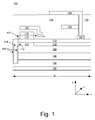
- FIG. 1 is an illustration of a portion of an electronic device that includes a high-electron-mobility transistor (HEMT) in embodiments according to the present invention.
- HEMT high-electron-mobility transistor
- FIG. 2 is an illustration of a portion of an electronic device that includes an HEMT in embodiments according to the present invention.
- FIGS. 3A and 3B are flowcharts of an example of a method for fabricating an HEMT in embodiments according to the present invention.
- FIG. 1 is an illustration of a cross-section of a portion of an electronic device that includes a high-electron-mobility transistor (HEMT) 100 in embodiments according to the present invention.
- the illustrated portion may be referred to as a cell.
- the HEMT 100 includes a first contact (source contact 102 ) on a first surface of a silicon substrate or layer 104 , and a number of layers on a second surface of the silicon layer (the second surface is opposite the first surface).
- the layers on the second surface of the silicon layer 104 include a buffer layer 106 , a first layer 108 that includes gallium, a two-dimensional electron gas (2DEG) layer 110 , and a second layer 112 that includes gallium.
- 2DEG two-dimensional electron gas
- the first layer 108 is composed of gallium nitride (GaN) and the second layer 112 is composed of aluminum GaN (AlGaN).
- GaN gallium nitride
- AlGaN aluminum GaN
- the present invention is not so limited. Materials other than GaN-based materials such as gallium arsenide (GaAs) and aluminum GaAs (AlGaAs) may be utilized in place of GaN and AlGaN, respectively.
- the buffer layer 106 includes aluminum nitride and alternating layers of AlGaN and GaN.
- the alternating layers in the buffer layer 106 may have different thicknesses.
- the source contact 102 is planar as shown in FIG. 1 and is composed of source metal.
- the silicon layer 104 is composed of highly conductive, very low resistance silicon. In an embodiment, the resistivity of the silicon in the silicon layer 104 is less than or equal to approximately one milliohm-centimeter.
- a gate contact 114 is disposed on the second layer 112 .
- the gate contact 114 extends from the second layer 112 , so that it is at least partially exposed relative to the second layer.
- the gate contact 114 includes a doped region 115 and a metal electrode 116 (an ohmic contact).
- the doped region 115 is composed of GaN that is doped to p-type with a p-type dopant such as, but not limited to, magnesium.
- the first layer 108 is in contact with the second layer 112 through an opening 111 in the 2DEG layer 110 .
- the ends of the opening 111 are substantially aligned with the edges of the gate contact 114 .
- a second contact (drain contact 124 ) is also disposed on the second layer 112 .
- the drain contact 124 extends from the second layer 112 , so that it is at least partially exposed relative to the second layer.
- the HEMT 100 includes a trench 118 that may be referred to herein as a buried interconnect.
- the trench 118 includes an insulating layer 120 and is filled with a conducting material such as metal.
- the metal may be tungsten, for example.
- the insulating layer 120 is composed of an insulating material (e.g., a dielectric) such as silicon nitride, for example.
- the trench 118 extends through the second layer 112 , the 2DEG layer 110 , the first layer 108 , and the buffer layer 106 into the silicon layer 104 .
- the insulating layer 120 is on the sidewalls of the trench 118 but is not on the top of the trench (at the second layer 112 ) or at the bottom of the trench (at the silicon layer 104 ).
- the conducting material in the trench 118 is in direct (electrical) contact with the silicon layer 104 .
- the trench 118 provides a path of less or least resistance between the upper surface (at the second layer 112 ) of the HEMT 100 and the source contact 102 .
- the insulating layer 120 is recessed so that the second layer 112 , the 2DEG layer 110 , and the conducting material in the trench 118 are in direct (electrical) contact. That is, the insulating layer 120 is disposed on the sidewalls of the trench 118 only between the conducting material in the trench and the first layer 108 , the buffer layer 106 , and the silicon layer 104 (but not at the bottom of the trench as described above).
- the trench 118 is separated from the gate contact 114 by a spacer 122 .
- the spacer 122 is composed of an insulating material and may be composed of the same insulating material used in the insulating layer 120 .
- the spacer 122 thus isolates the gate contact 114 from the trench 118 .
- the spacer 122 allows the gate contact 114 and the trench 118 to be fabricated as close as possible to each other (depending on the limitations of the fabrication process) without shorting the gate to the trench and source, thus reducing the cell width W.
- the HEMT 100 includes a passivation layer 128 , a first field plate 130 , and a second field plate 132 .
- the field plates 130 and 132 spread out the electrical field and mitigate peaking of the electrical field at the gate edge, extending the breakdown voltage of the device.
- the first field plate 130 is disposed within the passivation layer 128 , near the gate contact 114 , and is separated from the gate contact by a portion or region of the passivation layer.
- a metal interconnect 126 extends from the drain contact 124 through and out of the passivation layer 128 so that it is exposed outside of the passivation layer.
- the second field plate 132 is disposed between the drain contact 124 and the gate contact 114 and is connected to the metal interconnect 126 . Electrical connections to the gate contact 114 and to the first field plate 130 are in the z-direction.
- the HEMT 100 includes only a gate contact 114 and a drain contact 124 at the “top” surface (at or on the second layer 112 ) and a source contact 102 at the “bottom” surface (at or on the silicon layer 104 ). Consequently, source inductance, which is a major parasitic issue that can cause ringing in gate switching waveforms, is eliminated. Also, with the source contact 102 disposed at the bottom, source-to-gate metallization coupling is reduced or minimized, which significantly reduces parasitic effects.
- FIG. 2 is an illustration of a cross-section of a portion of an electronic device that includes an HEMT 200 in embodiments according to the present invention.
- the illustrated portion may be referred to as a cell.
- the HEMT 200 includes a first contact (drain contact 202 ) on a first surface of a silicon substrate or layer 204 , and a number of layers on a second surface of the silicon layer (the second surface is opposite the first surface).
- the layers on the second surface of the silicon layer 204 include a buffer layer 206 , a first layer 208 that includes gallium, a 2DEG layer 210 , and a second layer 212 that includes gallium.
- the first layer 208 is composed of GaN and the second layer 212 is composed of AlGaN.
- the present invention is not so limited. Materials other than GaN-based materials such as GaAs and AlGaAs may be utilized in place of GaN and AlGaN, respectively.
- the buffer layer 206 includes aluminum nitride and alternating layers of AlGaN and GaN.
- the alternating layers in the buffer layer 206 may have different thicknesses.
- the drain contact 202 is planar as shown in FIG. 2 and is composed of drain metal.
- the silicon layer 204 is composed of highly conductive, very low resistance silicon. In an embodiment, the resistivity of the silicon in the silicon layer 204 is less than or equal to approximately one milliohm-centimeter.
- a gate contact 214 is disposed on the second layer 212 .
- the gate contact 214 extends from the second layer 212 , so that it is at least partially exposed relative to the second layer.
- the gate contact 214 includes a doped region 215 and a metal electrode 216 (an ohmic contact).
- the doped region 215 is composed of GaN that is doped to p-type with a p-type dopant such as, but not limited to, magnesium.
- the first layer 208 is in contact with the second layer 212 through an opening 211 in the 2DEG layer 210 .
- the ends of the opening 211 are substantially aligned with the edges of the gate contact 214 .
- a second contact is also disposed on the second layer 212 .
- the source contact 224 extends from the second layer 212 , so that it is at least partially exposed relative to the second layer.
- the HEMT 200 includes a trench 218 that may be referred to herein as a buried interconnect.
- the trench 218 includes an insulating layer 220 and is filled with a conducting material such as metal.
- the metal may be tungsten, for example.
- the insulating layer 220 is composed of an insulating material (e.g., a dielectric) such as silicon nitride, for example. In an embodiment, the thickness of the insulating layer 220 is proportional to the drain voltage level.
- the trench 218 extends through the second layer 212 , the 2DEG layer 210 , the first layer 208 , and the buffer layer 206 into the silicon layer 204 .
- the insulating layer 220 is on the sidewalls of the trench 218 but is not on the top of the trench (at the second layer 212 ) or at the bottom of the trench (at the silicon layer 204 ).
- the conducting material in the trench 218 is in direct (electrical) contact with the silicon layer 204 .
- the trench 218 provides a path of less or least resistance between the upper surface (at the second layer 212 ) of the HEMT 200 and the drain contact 202 .
- the insulating layer 220 is recessed so that the second layer 21 , the 2DEG layer 210 , and the conducting material in the trench 218 are in direct (electrical) contact. That is, the insulating layer 220 is disposed on the sidewalls of the trench 218 only between the conducting material in the trench and the first layer 208 , the buffer layer 206 , and the silicon layer 204 (but not at the bottom of the trench as described above).
- the HEMT 200 includes a passivation layer 228 and a field plate 232 .
- the field plate 232 spreads out the electrical field, mitigates peaking of the electrical field at the gate edge, and extends the breakdown voltage of the device.
- the field plate 232 is disposed within the passivation layer 228 , near the gate contact 214 , and is separated from the gate contact by a portion or region of the passivation layer.
- a metal interconnect 230 extends from the source contact 224 through and out of the passivation layer 228 so that it is exposed outside of the passivation layer.
- the field plate 232 is connected to the metal interconnect 230 . Electrical connections to the gate contact 214 and the field plate 232 are in the z-direction.
- the HEMT 200 includes only a gate contact 214 and a source contact 224 at the “top” surface (at or on the second layer 212 ) and a drain contact 202 at the “bottom” surface (at or on the silicon layer 204 ). Because the drain metal is present only at the bottom of the HEMT 200 , the interaction between the gate metal and the drain metal is removed and there is no capacitive coupling between the drain contact 202 and either the gate or the source. Consequently, the parasitics between the drain contact 202 (the switching terminal) and the gate and the source are reduced or minimized. This results in fewer parasitic effects like gate ringing and improves device performance.
- FIGS. 1 and 2 provide other advantages.
- the HEMTs 100 and 200 have vertical structures as opposed to conventional lateral or planar structures, the number of levels of metal needed to route source, drain, and gate metal lines to their corresponding pads or terminals is reduced. Also, a special connection (either on the integrated circuit or chip or in the package) between the conductive silicon substrate and the appropriate electrical potential is not needed.
- cell width is reduced, meaning that cell density can be increased (more HEMTs can be placed in a given area relative to conventional, e.g., planar or lateral, structures).
- FIGS. 3A and 3B are flowcharts 300 of a method or process for fabricating a device (e.g., the HEMTs 100 and 200 of FIGS. 1 and 2 , respectively) in embodiments according to the present invention.
- FIGS. 3A and 3B are discussed in the context of a single cell, but can be readily extended to the fabrication in parallel of multiple such cells.
- a first contact is formed on a first surface of a substrate (silicon) layer.
- the first contact is a source contact.
- the first contact is a drain contact.
- a buffer layer is formed on a second surface of the substrate layer, where the second surface is opposite the first surface.
- a first layer that includes gallium is formed adjacent to the buffer layer.
- the first layer is grown epitaxially with metal-organic chemical vapor deposition (MOCVD).
- MOCVD metal-organic chemical vapor deposition
- a 2DEG layer is formed adjacent to the first layer.
- a second layer that includes gallium is formed adjacent to the 2DEG layer.
- the second layer is grown epitaxially with MOCVD.
- a second contact is formed on the second layer.
- the second contact is a drain contact.
- the second contact is a source contact.
- a gate contact is formed on the second layer.
- a trench is formed (e.g., plasma-etched or reactive ion-etched), where the trench has sidewalls that extend completely through the second layer, the 2DEG layer, the first layer, and the buffer layer and into the substrate layer, and has a bottom within the substrate layer.
- the sidewalls of the trench are lined with an insulating material.
- the insulating material is disposed such that, when the trench is filled with conducting material (block 320 ), the conducting material in the trench is in direct contact with the second layer, with the 2DEG layer, and with the substrate layer. This can be achieved by lining the sidewalls of the trench (not including the bottom of the trench) with insulating material only to the height of the bottom of the 2DEG layer, or by lining the sidewalls of the trench (not including the bottom of the trench) with insulating material to a height above the bottom of the 2DEG layer and then removing the insulating material to the bottom of the 2DEG layer.
- conducting material is deposited into the trench.
- remaining elements of the device are formed, such as but not limited to a passivation layer, field plates, and gate, source, and drain interconnects.
- a spacer is formed on the second layer next to the gate contact, and then the trench is formed next to the spacer.
- the trench is formed, and a liner insulator is then deposited into the trench and etched in such a way that it leaves the spacer next to the gate contact and along the sidewalls of the trench.
- FIGS. 3A and 3B operations described as separate blocks may be combined and performed in the same process step (that is, in the same time interval, after the preceding process step and before the next process step). Also, the operations may be performed in a different order than the order in which they are described below. Furthermore, fabrication processes and steps may be performed along with the processes and steps discussed herein; that is, there may be a number of process steps before, in between, and/or after the steps shown and described herein. Importantly, embodiments according to the present invention can be implemented in conjunction with these other (perhaps conventional) processes and steps without significantly perturbing them. Generally speaking, embodiments according to the present invention can replace portions of a conventional process without significantly affecting peripheral processes and steps.
- each cell of a device has only two terminals disposed at one (e.g., the upper) surface and a third terminal at the opposite (e.g., bottom) surface.
- HEMTs according to the present invention reduce the number of parasitic interconnections, simplify routing of the source, gate, and drain terminals, and permit increased cell densities.
Landscapes
- Engineering & Computer Science (AREA)
- Physics & Mathematics (AREA)
- Condensed Matter Physics & Semiconductors (AREA)
- General Physics & Mathematics (AREA)
- Computer Hardware Design (AREA)
- Microelectronics & Electronic Packaging (AREA)
- Power Engineering (AREA)
- Manufacturing & Machinery (AREA)
- Junction Field-Effect Transistors (AREA)
- Chemical & Material Sciences (AREA)
- Materials Engineering (AREA)
- Electrodes Of Semiconductors (AREA)
Abstract
Description
Claims (15)
Priority Applications (7)
| Application Number | Priority Date | Filing Date | Title |
|---|---|---|---|
| US15/643,328 US10381473B2 (en) | 2016-12-02 | 2017-07-06 | High-electron-mobility transistor with buried interconnect |
| EP17205012.2A EP3331027A3 (en) | 2016-12-02 | 2017-12-01 | High-electron-mobility transistor with buried interconnect |
| KR1020170163858A KR102197365B1 (en) | 2016-12-02 | 2017-12-01 | High-electron-mobility transistor with buried interconnect |
| EP22202778.1A EP4148806A1 (en) | 2016-12-02 | 2017-12-01 | High-electron-mobility transistor with buried interconnect |
| CN202211131635.6A CN115394650A (en) | 2016-12-02 | 2017-12-04 | High electron mobility transistor with buried interconnect |
| CN201711262724.3A CN108155233A (en) | 2016-12-02 | 2017-12-04 | High Electron Mobility Transistors with Buried Interconnects |
| US16/450,513 US10665711B2 (en) | 2016-12-02 | 2019-06-24 | High-electron-mobility transistor with buried interconnect |
Applications Claiming Priority (2)
| Application Number | Priority Date | Filing Date | Title |
|---|---|---|---|
| US201662429629P | 2016-12-02 | 2016-12-02 | |
| US15/643,328 US10381473B2 (en) | 2016-12-02 | 2017-07-06 | High-electron-mobility transistor with buried interconnect |
Related Child Applications (1)
| Application Number | Title | Priority Date | Filing Date |
|---|---|---|---|
| US16/450,513 Division US10665711B2 (en) | 2016-12-02 | 2019-06-24 | High-electron-mobility transistor with buried interconnect |
Publications (2)
| Publication Number | Publication Date |
|---|---|
| US20180158942A1 US20180158942A1 (en) | 2018-06-07 |
| US10381473B2 true US10381473B2 (en) | 2019-08-13 |
Family
ID=60569755
Family Applications (2)
| Application Number | Title | Priority Date | Filing Date |
|---|---|---|---|
| US15/643,328 Active US10381473B2 (en) | 2016-12-02 | 2017-07-06 | High-electron-mobility transistor with buried interconnect |
| US16/450,513 Active US10665711B2 (en) | 2016-12-02 | 2019-06-24 | High-electron-mobility transistor with buried interconnect |
Family Applications After (1)
| Application Number | Title | Priority Date | Filing Date |
|---|---|---|---|
| US16/450,513 Active US10665711B2 (en) | 2016-12-02 | 2019-06-24 | High-electron-mobility transistor with buried interconnect |
Country Status (4)
| Country | Link |
|---|---|
| US (2) | US10381473B2 (en) |
| EP (2) | EP4148806A1 (en) |
| KR (1) | KR102197365B1 (en) |
| CN (2) | CN115394650A (en) |
Cited By (1)
| Publication number | Priority date | Publication date | Assignee | Title |
|---|---|---|---|---|
| US20220231157A1 (en) * | 2019-05-30 | 2022-07-21 | Gpower Semiconductor, Inc. | Semiconductor device, method of manufacturing the same, and semiconductor package structure |
Families Citing this family (12)
| Publication number | Priority date | Publication date | Assignee | Title |
|---|---|---|---|---|
| US10224426B2 (en) | 2016-12-02 | 2019-03-05 | Vishay-Siliconix | High-electron-mobility transistor devices |
| US10381473B2 (en) | 2016-12-02 | 2019-08-13 | Vishay-Siliconix | High-electron-mobility transistor with buried interconnect |
| US11257811B2 (en) | 2017-07-14 | 2022-02-22 | Cambridge Enterprise Limited | Power semiconductor device with an auxiliary gate structure |
| GB2564482B (en) | 2017-07-14 | 2021-02-10 | Cambridge Entpr Ltd | A power semiconductor device with a double gate structure |
| US11336279B2 (en) | 2017-07-14 | 2022-05-17 | Cambridge Enterprise Limited | Power semiconductor device with a series connection of two devices |
| US10833063B2 (en) | 2018-07-25 | 2020-11-10 | Vishay SIliconix, LLC | High electron mobility transistor ESD protection structures |
| EP3671825A1 (en) | 2018-12-20 | 2020-06-24 | IMEC vzw | Method for connecting a buried interconnect rail and a semiconductor fin in an integrated circuit chip |
| US12382651B2 (en) | 2019-05-07 | 2025-08-05 | Cambridge Gan Devices Limited | Power semiconductor device with an auxiliary gate structure |
| US11955478B2 (en) * | 2019-05-07 | 2024-04-09 | Cambridge Gan Devices Limited | Power semiconductor device with an auxiliary gate structure |
| CN113809160A (en) * | 2021-08-25 | 2021-12-17 | 西安电子科技大学 | A kind of gold-free field plate GaN-based radio frequency device and its manufacturing method |
| CN116190412A (en) * | 2021-11-29 | 2023-05-30 | 中国科学院苏州纳米技术与纳米仿生研究所 | Device structure and manufacturing method of a high electron mobility transistor |
| CN117457735A (en) * | 2023-12-22 | 2024-01-26 | 英诺赛科(珠海)科技有限公司 | Transistor structure and manufacturing method and chip |
Citations (33)
| Publication number | Priority date | Publication date | Assignee | Title |
|---|---|---|---|---|
| US20020020873A1 (en) | 2000-08-08 | 2002-02-21 | Advanced Power Technology, Inc. | Power MOS device with asymmetrical channel structure for enhanced linear operation capability |
| US20060108659A1 (en) | 2004-11-25 | 2006-05-25 | Matsushita Electric Industrial Co., Ltd. | Schottky barrier diode and diode array |
| US20080142837A1 (en) | 2006-11-09 | 2008-06-19 | The Furukawa Electric Co., Ltd. | Vertical type semiconductor device and manufacturing method of the device |
| US20080296618A1 (en) | 2007-06-01 | 2008-12-04 | The Regents Of The University Of California | P-GaN/AlGaN/AlN/GaN ENHANCEMENT-MODE FIELD EFFECT TRANSISTOR |
| US20090065785A1 (en) | 2007-09-06 | 2009-03-12 | Robert Beach | III-nitride power semiconductor device |
| US20090140295A1 (en) | 2007-11-16 | 2009-06-04 | Shusuke Kaya | GaN-based semiconductor device and method of manufacturing the same |
| US20090166677A1 (en) * | 2007-12-28 | 2009-07-02 | Daisuke Shibata | Semiconductor device and manufacturing method thereof |
| US7781894B2 (en) | 2005-12-06 | 2010-08-24 | Sanyo Electric Co., Ltd. | Semiconductor device and manufacturing method of same |
| US7816764B2 (en) | 2000-08-04 | 2010-10-19 | The Regents Of The University Of California | Method of controlling stress in gallium nitride films deposited on substrates |
| US7851825B2 (en) | 2007-12-10 | 2010-12-14 | Transphorm Inc. | Insulated gate e-mode transistors |
| US7898004B2 (en) | 2008-12-10 | 2011-03-01 | Transphorm Inc. | Semiconductor heterostructure diodes |
| US20110101370A1 (en) | 2009-10-30 | 2011-05-05 | Imec | Semiconductor device and method of manufacturing thereof |
| US7985986B2 (en) | 2008-07-31 | 2011-07-26 | Cree, Inc. | Normally-off semiconductor devices |
| US20110210337A1 (en) * | 2010-03-01 | 2011-09-01 | International Rectifier Corporation | Monolithic integration of silicon and group III-V devices |
| US8039352B2 (en) | 2007-05-24 | 2011-10-18 | The Regents Of The University Of California | Polarization-induced barriers for N-face nitride-based electronics |
| US8049252B2 (en) | 2006-01-17 | 2011-11-01 | Cree, Inc. | Methods of fabricating transistors including dielectrically-supported gate electrodes and related devices |
| US20120007049A1 (en) | 2010-07-07 | 2012-01-12 | Samsung Electro-Mechanics Co., Ltd. | Nitride-based semiconductor device and method for manufacturing the same |
| US8114717B2 (en) | 2005-11-15 | 2012-02-14 | The Regents Of The University Of California | Methods to shape the electric field in electron devices, passivate dislocations and point defects, and enhance the luminescence efficiency of optical devices |
| US20120043586A1 (en) * | 2010-08-23 | 2012-02-23 | Fujitsu Limited | Semiconductor device and method for manufacturing the same |
| US20120080724A1 (en) | 2010-10-05 | 2012-04-05 | Sanken Electric Co., Ltd. | Semiconductor device |
| US8390027B2 (en) | 2007-10-01 | 2013-03-05 | Fuji Electric Co., Ltd. | Gallium nitride semiconductor device and manufacturing method thereof |
| US20130088280A1 (en) | 2011-10-07 | 2013-04-11 | Transphorm Inc. | High power semiconductor electronic components with increased reliability |
| US20130153919A1 (en) | 2011-12-20 | 2013-06-20 | Infineon Technologies Austria Ag | III-V Semiconductor Devices with Buried Contacts |
| US8587033B1 (en) | 2012-06-04 | 2013-11-19 | Infineon Technologies Austria Ag | Monolithically integrated HEMT and current protection device |
| EP2779246A2 (en) | 2013-03-15 | 2014-09-17 | Semiconductor Components Industries, LLC | Method of forming a high electron mobility semiconductor device and structure therefor |
| US20150069615A1 (en) | 2013-09-12 | 2015-03-12 | Kabushiki Kaisha Toshiba | Semiconductor device |
| US9083175B2 (en) | 2012-05-16 | 2015-07-14 | Nxp, B.V. | Protection circuit |
| US9142543B2 (en) | 2013-02-06 | 2015-09-22 | Seiko Instruments Inc. | Semiconductor device having an ESD protection circuit |
| US9331472B2 (en) | 2011-11-09 | 2016-05-03 | Mediatek Inc | ESD protection circuit |
| US20170357283A1 (en) | 2016-06-08 | 2017-12-14 | Panasonic Corporation | Substrate voltage control circuit |
| US20180047719A1 (en) | 2013-05-23 | 2018-02-15 | Infineon Technologies Austria Ag | Method of Manufacturing a Semiconductor Die |
| US9941267B2 (en) | 2014-09-09 | 2018-04-10 | Taiwan Semiconductor Manufacturing Company Limited | Electro-static discharge protection circuit |
| US20180151681A1 (en) | 2016-11-28 | 2018-05-31 | Infineon Technologies Austria Ag | Normally Off HEMT with Self Aligned Gate Structure |
Family Cites Families (22)
| Publication number | Priority date | Publication date | Assignee | Title |
|---|---|---|---|---|
| KR100348902B1 (en) * | 1999-11-30 | 2002-08-14 | 한국전자통신연구원 | Method of manufacturing a gamma gate of hemt |
| US6527938B2 (en) | 2001-06-21 | 2003-03-04 | Syntheon, Llc | Method for microporous surface modification of implantable metallic medical articles |
| US8629019B2 (en) | 2002-09-24 | 2014-01-14 | Vishay-Siliconix | Method of forming self aligned contacts for a power MOSFET |
| US11791385B2 (en) * | 2005-03-11 | 2023-10-17 | Wolfspeed, Inc. | Wide bandgap transistors with gate-source field plates |
| US7583485B1 (en) | 2005-07-26 | 2009-09-01 | Vishay-Siliconix | Electrostatic discharge protection circuit for integrated circuits |
| US7544545B2 (en) | 2005-12-28 | 2009-06-09 | Vishay-Siliconix | Trench polysilicon diode |
| WO2007084688A1 (en) | 2006-01-18 | 2007-07-26 | Vishay-Siliconix | Floating gate structure with high electrostatic discharge performance |
| WO2008096521A1 (en) * | 2007-02-07 | 2008-08-14 | Nec Corporation | Semiconductor device |
| KR100922575B1 (en) * | 2007-12-05 | 2009-10-21 | 한국전자통신연구원 | A semiconductor device having a tee gate electrode and a method of manufacturing the same |
| JP2010103236A (en) * | 2008-10-22 | 2010-05-06 | Panasonic Corp | Nitride semiconductor device |
| US8269019B2 (en) | 2010-03-10 | 2012-09-18 | Probiodrug Ag | Inhibitors |
| JP5837499B2 (en) * | 2010-08-20 | 2015-12-24 | シャープ株式会社 | Inverter |
| US8088660B1 (en) * | 2010-12-15 | 2012-01-03 | Infineon Technologies Austria Ag | Method for producing a plug in a semiconductor body |
| CN102738228A (en) * | 2012-06-28 | 2012-10-17 | 电子科技大学 | High electron mobility transistor (HEMT) with gate edge groove type source field plate structure |
| US20140026445A1 (en) * | 2012-07-24 | 2014-01-30 | Greg Schlichte | Integral climbing boot |
| JP6174874B2 (en) * | 2013-03-15 | 2017-08-02 | ルネサスエレクトロニクス株式会社 | Semiconductor device |
| KR102065113B1 (en) | 2013-05-01 | 2020-01-10 | 삼성전자주식회사 | High electron mobility transistor and method of driving the same |
| KR102067597B1 (en) * | 2013-05-27 | 2020-01-17 | 엘지전자 주식회사 | Nitride semiconductor and method thereof |
| US9306014B1 (en) * | 2013-12-27 | 2016-04-05 | Power Integrations, Inc. | High-electron-mobility transistors |
| US9748224B2 (en) * | 2014-10-28 | 2017-08-29 | Semiconductor Components Industries, Llc | Heterojunction semiconductor device having integrated clamping device |
| US10224426B2 (en) | 2016-12-02 | 2019-03-05 | Vishay-Siliconix | High-electron-mobility transistor devices |
| US10381473B2 (en) | 2016-12-02 | 2019-08-13 | Vishay-Siliconix | High-electron-mobility transistor with buried interconnect |
-
2017
- 2017-07-06 US US15/643,328 patent/US10381473B2/en active Active
- 2017-12-01 KR KR1020170163858A patent/KR102197365B1/en active Active
- 2017-12-01 EP EP22202778.1A patent/EP4148806A1/en active Pending
- 2017-12-01 EP EP17205012.2A patent/EP3331027A3/en not_active Ceased
- 2017-12-04 CN CN202211131635.6A patent/CN115394650A/en active Pending
- 2017-12-04 CN CN201711262724.3A patent/CN108155233A/en active Pending
-
2019
- 2019-06-24 US US16/450,513 patent/US10665711B2/en active Active
Patent Citations (34)
| Publication number | Priority date | Publication date | Assignee | Title |
|---|---|---|---|---|
| US7816764B2 (en) | 2000-08-04 | 2010-10-19 | The Regents Of The University Of California | Method of controlling stress in gallium nitride films deposited on substrates |
| US20020020873A1 (en) | 2000-08-08 | 2002-02-21 | Advanced Power Technology, Inc. | Power MOS device with asymmetrical channel structure for enhanced linear operation capability |
| US20060108659A1 (en) | 2004-11-25 | 2006-05-25 | Matsushita Electric Industrial Co., Ltd. | Schottky barrier diode and diode array |
| US8114717B2 (en) | 2005-11-15 | 2012-02-14 | The Regents Of The University Of California | Methods to shape the electric field in electron devices, passivate dislocations and point defects, and enhance the luminescence efficiency of optical devices |
| US7781894B2 (en) | 2005-12-06 | 2010-08-24 | Sanyo Electric Co., Ltd. | Semiconductor device and manufacturing method of same |
| US8049252B2 (en) | 2006-01-17 | 2011-11-01 | Cree, Inc. | Methods of fabricating transistors including dielectrically-supported gate electrodes and related devices |
| US20080142837A1 (en) | 2006-11-09 | 2008-06-19 | The Furukawa Electric Co., Ltd. | Vertical type semiconductor device and manufacturing method of the device |
| US8039352B2 (en) | 2007-05-24 | 2011-10-18 | The Regents Of The University Of California | Polarization-induced barriers for N-face nitride-based electronics |
| US20080296618A1 (en) | 2007-06-01 | 2008-12-04 | The Regents Of The University Of California | P-GaN/AlGaN/AlN/GaN ENHANCEMENT-MODE FIELD EFFECT TRANSISTOR |
| US20090065785A1 (en) | 2007-09-06 | 2009-03-12 | Robert Beach | III-nitride power semiconductor device |
| US8390027B2 (en) | 2007-10-01 | 2013-03-05 | Fuji Electric Co., Ltd. | Gallium nitride semiconductor device and manufacturing method thereof |
| US20090140295A1 (en) | 2007-11-16 | 2009-06-04 | Shusuke Kaya | GaN-based semiconductor device and method of manufacturing the same |
| US7851825B2 (en) | 2007-12-10 | 2010-12-14 | Transphorm Inc. | Insulated gate e-mode transistors |
| US20090166677A1 (en) * | 2007-12-28 | 2009-07-02 | Daisuke Shibata | Semiconductor device and manufacturing method thereof |
| US7985986B2 (en) | 2008-07-31 | 2011-07-26 | Cree, Inc. | Normally-off semiconductor devices |
| US7898004B2 (en) | 2008-12-10 | 2011-03-01 | Transphorm Inc. | Semiconductor heterostructure diodes |
| US20110101370A1 (en) | 2009-10-30 | 2011-05-05 | Imec | Semiconductor device and method of manufacturing thereof |
| US20110210337A1 (en) * | 2010-03-01 | 2011-09-01 | International Rectifier Corporation | Monolithic integration of silicon and group III-V devices |
| US20120007049A1 (en) | 2010-07-07 | 2012-01-12 | Samsung Electro-Mechanics Co., Ltd. | Nitride-based semiconductor device and method for manufacturing the same |
| US20120043586A1 (en) * | 2010-08-23 | 2012-02-23 | Fujitsu Limited | Semiconductor device and method for manufacturing the same |
| US20120080724A1 (en) | 2010-10-05 | 2012-04-05 | Sanken Electric Co., Ltd. | Semiconductor device |
| US20130088280A1 (en) | 2011-10-07 | 2013-04-11 | Transphorm Inc. | High power semiconductor electronic components with increased reliability |
| US9331472B2 (en) | 2011-11-09 | 2016-05-03 | Mediatek Inc | ESD protection circuit |
| US20130153919A1 (en) | 2011-12-20 | 2013-06-20 | Infineon Technologies Austria Ag | III-V Semiconductor Devices with Buried Contacts |
| US9083175B2 (en) | 2012-05-16 | 2015-07-14 | Nxp, B.V. | Protection circuit |
| US8587033B1 (en) | 2012-06-04 | 2013-11-19 | Infineon Technologies Austria Ag | Monolithically integrated HEMT and current protection device |
| US9142543B2 (en) | 2013-02-06 | 2015-09-22 | Seiko Instruments Inc. | Semiconductor device having an ESD protection circuit |
| US20140264453A1 (en) * | 2013-03-15 | 2014-09-18 | Semiconductor Components Industries, Llc | Method of forming a high electron mobility semiconductor device and structure therefor |
| EP2779246A2 (en) | 2013-03-15 | 2014-09-17 | Semiconductor Components Industries, LLC | Method of forming a high electron mobility semiconductor device and structure therefor |
| US20180047719A1 (en) | 2013-05-23 | 2018-02-15 | Infineon Technologies Austria Ag | Method of Manufacturing a Semiconductor Die |
| US20150069615A1 (en) | 2013-09-12 | 2015-03-12 | Kabushiki Kaisha Toshiba | Semiconductor device |
| US9941267B2 (en) | 2014-09-09 | 2018-04-10 | Taiwan Semiconductor Manufacturing Company Limited | Electro-static discharge protection circuit |
| US20170357283A1 (en) | 2016-06-08 | 2017-12-14 | Panasonic Corporation | Substrate voltage control circuit |
| US20180151681A1 (en) | 2016-11-28 | 2018-05-31 | Infineon Technologies Austria Ag | Normally Off HEMT with Self Aligned Gate Structure |
Non-Patent Citations (3)
| Title |
|---|
| Lee, Finella; The Effects of Gate Metals on the Performance of p-GaN/AlGaN/GaN High Electron Mobility Transistors; Mantech Conference; May 19, 2014; Denver Colorado, US. |
| Meneghini, Matteo; Technology and Reliability of Normally-Off GaN HEMTs with p-Type Gate; Energies, MDPI; Journal; Jan. 24, 2017; Basel, CH. |
| Wuerfl et al., "Reliability issues of Gan based high voltage power devices", Microelectronics and Reliability, Elsevier Science LTD., vol. 51, No. 9, Jul. 5, 2011, Berlin, Germany. |
Cited By (2)
| Publication number | Priority date | Publication date | Assignee | Title |
|---|---|---|---|---|
| US20220231157A1 (en) * | 2019-05-30 | 2022-07-21 | Gpower Semiconductor, Inc. | Semiconductor device, method of manufacturing the same, and semiconductor package structure |
| US12272743B2 (en) * | 2019-05-30 | 2025-04-08 | Gpower Semiconductor, Inc. | Semiconductor device comprising a drain back contact electrode, method of manufacturing the same, and semiconductor package structure |
Also Published As
| Publication number | Publication date |
|---|---|
| EP3331027A3 (en) | 2018-10-24 |
| EP4148806A1 (en) | 2023-03-15 |
| KR20180063837A (en) | 2018-06-12 |
| US20180158942A1 (en) | 2018-06-07 |
| KR102197365B1 (en) | 2020-12-31 |
| US20190312137A1 (en) | 2019-10-10 |
| EP3331027A2 (en) | 2018-06-06 |
| CN115394650A (en) | 2022-11-25 |
| CN108155233A (en) | 2018-06-12 |
| US10665711B2 (en) | 2020-05-26 |
Similar Documents
| Publication | Publication Date | Title |
|---|---|---|
| US10665711B2 (en) | High-electron-mobility transistor with buried interconnect | |
| US20230420526A1 (en) | Wide bandgap transistors with gate-source field plates | |
| US9887268B2 (en) | Capacitively-coupled field-plate structures for semiconductor devices | |
| JP5755671B2 (en) | Wide band gap transistor with multiple field plates | |
| US12446252B2 (en) | Transistors including semiconductor surface modification and related fabrication methods | |
| CN104319238B (en) | Form the method and its structure of high electron mobility semiconductor device | |
| US12471341B2 (en) | Method of fabricating a semiconductor device | |
| US11695052B2 (en) | III-Nitride transistor with a cap layer for RF operation | |
| US10985253B2 (en) | Semiconductor devices with multiple channels and three-dimensional electrodes | |
| US10971615B2 (en) | High power performance gallium nitride high electron mobility transistor with ledges and field plates | |
| EP3185295A1 (en) | Semiconductor package structure based on cascade circuits | |
| CN117594595A (en) | Integrated depletion-mode and enhancement-mode gallium nitride high electron mobility transistor | |
| KR20200144496A (en) | Semiconductor device and method for fabricating a wafer | |
| US12218202B2 (en) | Semiconductor device incorporating a substrate recess | |
| US12211912B2 (en) | Semiconductor device and fabrication method thereof | |
| WO2026035596A1 (en) | Gallium nitride-based semiconductor devices with dielectric segments and methods of fabrication thereof |
Legal Events
| Date | Code | Title | Description |
|---|---|---|---|
| AS | Assignment |
Owner name: VISHAY-SILICONIX, CALIFORNIA Free format text: ASSIGNMENT OF ASSIGNORS INTEREST;ASSIGNORS:SHIBIB, AYMAN;TERRILL, KYLE;DING, YONGPING;AND OTHERS;REEL/FRAME:042927/0022 Effective date: 20170616 |
|
| STPP | Information on status: patent application and granting procedure in general |
Free format text: NOTICE OF ALLOWANCE MAILED -- APPLICATION RECEIVED IN OFFICE OF PUBLICATIONS |
|
| AS | Assignment |
Owner name: JPMORGAN CHASE BANK, N.A., AS ADMINISTRATIVE AGENT Free format text: SECURITY INTEREST;ASSIGNORS:VISHAY DALE ELECTRONICS, INC.;DALE ELECTRONICS, INC.;VISHAY DALE ELECTRONICS, LLC;AND OTHERS;REEL/FRAME:049440/0876 Effective date: 20190605 Owner name: JPMORGAN CHASE BANK, N.A., AS ADMINISTRATIVE AGENT, ILLINOIS Free format text: SECURITY INTEREST;ASSIGNORS:VISHAY DALE ELECTRONICS, INC.;DALE ELECTRONICS, INC.;VISHAY DALE ELECTRONICS, LLC;AND OTHERS;REEL/FRAME:049440/0876 Effective date: 20190605 |
|
| STCF | Information on status: patent grant |
Free format text: PATENTED CASE |
|
| MAFP | Maintenance fee payment |
Free format text: PAYMENT OF MAINTENANCE FEE, 4TH YEAR, LARGE ENTITY (ORIGINAL EVENT CODE: M1551); ENTITY STATUS OF PATENT OWNER: LARGE ENTITY Year of fee payment: 4 |