US10157786B2 - Selective formation of metallic films on metallic surfaces - Google Patents
Selective formation of metallic films on metallic surfaces Download PDFInfo
- Publication number
- US10157786B2 US10157786B2 US15/356,306 US201615356306A US10157786B2 US 10157786 B2 US10157786 B2 US 10157786B2 US 201615356306 A US201615356306 A US 201615356306A US 10157786 B2 US10157786 B2 US 10157786B2
- Authority
- US
- United States
- Prior art keywords
- substrate
- deposition
- metal
- dielectric
- precursor
- Prior art date
- Legal status (The legal status is an assumption and is not a legal conclusion. Google has not performed a legal analysis and makes no representation as to the accuracy of the status listed.)
- Active
Links
Images


Classifications
-
- H—ELECTRICITY
- H01—ELECTRIC ELEMENTS
- H01L—SEMICONDUCTOR DEVICES NOT COVERED BY CLASS H10
- H01L21/00—Processes or apparatus adapted for the manufacture or treatment of semiconductor or solid state devices or of parts thereof
- H01L21/70—Manufacture or treatment of devices consisting of a plurality of solid state components formed in or on a common substrate or of parts thereof; Manufacture of integrated circuit devices or of parts thereof
- H01L21/71—Manufacture of specific parts of devices defined in group H01L21/70
- H01L21/768—Applying interconnections to be used for carrying current between separate components within a device comprising conductors and dielectrics
- H01L21/76838—Applying interconnections to be used for carrying current between separate components within a device comprising conductors and dielectrics characterised by the formation and the after-treatment of the conductors
- H01L21/76841—Barrier, adhesion or liner layers
- H01L21/7685—Barrier, adhesion or liner layers the layer covering a conductive structure
-
- H10W20/038—
-
- C—CHEMISTRY; METALLURGY
- C23—COATING METALLIC MATERIAL; COATING MATERIAL WITH METALLIC MATERIAL; CHEMICAL SURFACE TREATMENT; DIFFUSION TREATMENT OF METALLIC MATERIAL; COATING BY VACUUM EVAPORATION, BY SPUTTERING, BY ION IMPLANTATION OR BY CHEMICAL VAPOUR DEPOSITION, IN GENERAL; INHIBITING CORROSION OF METALLIC MATERIAL OR INCRUSTATION IN GENERAL
- C23C—COATING METALLIC MATERIAL; COATING MATERIAL WITH METALLIC MATERIAL; SURFACE TREATMENT OF METALLIC MATERIAL BY DIFFUSION INTO THE SURFACE, BY CHEMICAL CONVERSION OR SUBSTITUTION; COATING BY VACUUM EVAPORATION, BY SPUTTERING, BY ION IMPLANTATION OR BY CHEMICAL VAPOUR DEPOSITION, IN GENERAL
- C23C16/00—Chemical coating by decomposition of gaseous compounds, without leaving reaction products of surface material in the coating, i.e. chemical vapour deposition [CVD] processes
- C23C16/04—Coating on selected surface areas, e.g. using masks
-
- C—CHEMISTRY; METALLURGY
- C23—COATING METALLIC MATERIAL; COATING MATERIAL WITH METALLIC MATERIAL; CHEMICAL SURFACE TREATMENT; DIFFUSION TREATMENT OF METALLIC MATERIAL; COATING BY VACUUM EVAPORATION, BY SPUTTERING, BY ION IMPLANTATION OR BY CHEMICAL VAPOUR DEPOSITION, IN GENERAL; INHIBITING CORROSION OF METALLIC MATERIAL OR INCRUSTATION IN GENERAL
- C23C—COATING METALLIC MATERIAL; COATING MATERIAL WITH METALLIC MATERIAL; SURFACE TREATMENT OF METALLIC MATERIAL BY DIFFUSION INTO THE SURFACE, BY CHEMICAL CONVERSION OR SUBSTITUTION; COATING BY VACUUM EVAPORATION, BY SPUTTERING, BY ION IMPLANTATION OR BY CHEMICAL VAPOUR DEPOSITION, IN GENERAL
- C23C16/00—Chemical coating by decomposition of gaseous compounds, without leaving reaction products of surface material in the coating, i.e. chemical vapour deposition [CVD] processes
- C23C16/06—Chemical coating by decomposition of gaseous compounds, without leaving reaction products of surface material in the coating, i.e. chemical vapour deposition [CVD] processes characterised by the deposition of metallic material
- C23C16/08—Chemical coating by decomposition of gaseous compounds, without leaving reaction products of surface material in the coating, i.e. chemical vapour deposition [CVD] processes characterised by the deposition of metallic material from metal halides
- C23C16/14—Deposition of only one other metal element
-
- C—CHEMISTRY; METALLURGY
- C23—COATING METALLIC MATERIAL; COATING MATERIAL WITH METALLIC MATERIAL; CHEMICAL SURFACE TREATMENT; DIFFUSION TREATMENT OF METALLIC MATERIAL; COATING BY VACUUM EVAPORATION, BY SPUTTERING, BY ION IMPLANTATION OR BY CHEMICAL VAPOUR DEPOSITION, IN GENERAL; INHIBITING CORROSION OF METALLIC MATERIAL OR INCRUSTATION IN GENERAL
- C23C—COATING METALLIC MATERIAL; COATING MATERIAL WITH METALLIC MATERIAL; SURFACE TREATMENT OF METALLIC MATERIAL BY DIFFUSION INTO THE SURFACE, BY CHEMICAL CONVERSION OR SUBSTITUTION; COATING BY VACUUM EVAPORATION, BY SPUTTERING, BY ION IMPLANTATION OR BY CHEMICAL VAPOUR DEPOSITION, IN GENERAL
- C23C16/00—Chemical coating by decomposition of gaseous compounds, without leaving reaction products of surface material in the coating, i.e. chemical vapour deposition [CVD] processes
- C23C16/44—Chemical coating by decomposition of gaseous compounds, without leaving reaction products of surface material in the coating, i.e. chemical vapour deposition [CVD] processes characterised by the method of coating
- C23C16/455—Chemical coating by decomposition of gaseous compounds, without leaving reaction products of surface material in the coating, i.e. chemical vapour deposition [CVD] processes characterised by the method of coating characterised by the method used for introducing gases into reaction chamber or for modifying gas flows in reaction chamber
- C23C16/45523—Pulsed gas flow or change of composition over time
- C23C16/45525—Atomic layer deposition [ALD]
- C23C16/45527—Atomic layer deposition [ALD] characterized by the ALD cycle, e.g. different flows or temperatures during half-reactions, unusual pulsing sequence, use of precursor mixtures or auxiliary reactants or activations
- C23C16/45536—Use of plasma, radiation or electromagnetic fields
-
- C—CHEMISTRY; METALLURGY
- C23—COATING METALLIC MATERIAL; COATING MATERIAL WITH METALLIC MATERIAL; CHEMICAL SURFACE TREATMENT; DIFFUSION TREATMENT OF METALLIC MATERIAL; COATING BY VACUUM EVAPORATION, BY SPUTTERING, BY ION IMPLANTATION OR BY CHEMICAL VAPOUR DEPOSITION, IN GENERAL; INHIBITING CORROSION OF METALLIC MATERIAL OR INCRUSTATION IN GENERAL
- C23C—COATING METALLIC MATERIAL; COATING MATERIAL WITH METALLIC MATERIAL; SURFACE TREATMENT OF METALLIC MATERIAL BY DIFFUSION INTO THE SURFACE, BY CHEMICAL CONVERSION OR SUBSTITUTION; COATING BY VACUUM EVAPORATION, BY SPUTTERING, BY ION IMPLANTATION OR BY CHEMICAL VAPOUR DEPOSITION, IN GENERAL
- C23C16/00—Chemical coating by decomposition of gaseous compounds, without leaving reaction products of surface material in the coating, i.e. chemical vapour deposition [CVD] processes
- C23C16/44—Chemical coating by decomposition of gaseous compounds, without leaving reaction products of surface material in the coating, i.e. chemical vapour deposition [CVD] processes characterised by the method of coating
- C23C16/455—Chemical coating by decomposition of gaseous compounds, without leaving reaction products of surface material in the coating, i.e. chemical vapour deposition [CVD] processes characterised by the method of coating characterised by the method used for introducing gases into reaction chamber or for modifying gas flows in reaction chamber
- C23C16/45523—Pulsed gas flow or change of composition over time
- C23C16/45525—Atomic layer deposition [ALD]
- C23C16/45553—Atomic layer deposition [ALD] characterized by the use of precursors specially adapted for ALD
-
- H—ELECTRICITY
- H01—ELECTRIC ELEMENTS
- H01L—SEMICONDUCTOR DEVICES NOT COVERED BY CLASS H10
- H01L21/00—Processes or apparatus adapted for the manufacture or treatment of semiconductor or solid state devices or of parts thereof
- H01L21/02—Manufacture or treatment of semiconductor devices or of parts thereof
- H01L21/02041—Cleaning
- H01L21/02057—Cleaning during device manufacture
- H01L21/02068—Cleaning during device manufacture during, before or after processing of conductive layers, e.g. polysilicon or amorphous silicon layers
-
- H—ELECTRICITY
- H01—ELECTRIC ELEMENTS
- H01L—SEMICONDUCTOR DEVICES NOT COVERED BY CLASS H10
- H01L21/00—Processes or apparatus adapted for the manufacture or treatment of semiconductor or solid state devices or of parts thereof
- H01L21/02—Manufacture or treatment of semiconductor devices or of parts thereof
- H01L21/04—Manufacture or treatment of semiconductor devices or of parts thereof the devices having potential barriers, e.g. a PN junction, depletion layer or carrier concentration layer
- H01L21/18—Manufacture or treatment of semiconductor devices or of parts thereof the devices having potential barriers, e.g. a PN junction, depletion layer or carrier concentration layer the devices having semiconductor bodies comprising elements of Group IV of the Periodic Table or AIIIBV compounds with or without impurities, e.g. doping materials
- H01L21/28—Manufacture of electrodes on semiconductor bodies using processes or apparatus not provided for in groups H01L21/20 - H01L21/268
- H01L21/283—Deposition of conductive or insulating materials for electrodes conducting electric current
- H01L21/285—Deposition of conductive or insulating materials for electrodes conducting electric current from a gas or vapour, e.g. condensation
- H01L21/28506—Deposition of conductive or insulating materials for electrodes conducting electric current from a gas or vapour, e.g. condensation of conductive layers
- H01L21/28512—Deposition of conductive or insulating materials for electrodes conducting electric current from a gas or vapour, e.g. condensation of conductive layers on semiconductor bodies comprising elements of Group IV of the Periodic Table
- H01L21/28518—Deposition of conductive or insulating materials for electrodes conducting electric current from a gas or vapour, e.g. condensation of conductive layers on semiconductor bodies comprising elements of Group IV of the Periodic Table the conductive layers comprising silicides
-
- H—ELECTRICITY
- H01—ELECTRIC ELEMENTS
- H01L—SEMICONDUCTOR DEVICES NOT COVERED BY CLASS H10
- H01L21/00—Processes or apparatus adapted for the manufacture or treatment of semiconductor or solid state devices or of parts thereof
- H01L21/02—Manufacture or treatment of semiconductor devices or of parts thereof
- H01L21/04—Manufacture or treatment of semiconductor devices or of parts thereof the devices having potential barriers, e.g. a PN junction, depletion layer or carrier concentration layer
- H01L21/18—Manufacture or treatment of semiconductor devices or of parts thereof the devices having potential barriers, e.g. a PN junction, depletion layer or carrier concentration layer the devices having semiconductor bodies comprising elements of Group IV of the Periodic Table or AIIIBV compounds with or without impurities, e.g. doping materials
- H01L21/28—Manufacture of electrodes on semiconductor bodies using processes or apparatus not provided for in groups H01L21/20 - H01L21/268
- H01L21/283—Deposition of conductive or insulating materials for electrodes conducting electric current
- H01L21/285—Deposition of conductive or insulating materials for electrodes conducting electric current from a gas or vapour, e.g. condensation
- H01L21/28506—Deposition of conductive or insulating materials for electrodes conducting electric current from a gas or vapour, e.g. condensation of conductive layers
- H01L21/28512—Deposition of conductive or insulating materials for electrodes conducting electric current from a gas or vapour, e.g. condensation of conductive layers on semiconductor bodies comprising elements of Group IV of the Periodic Table
- H01L21/28556—Deposition of conductive or insulating materials for electrodes conducting electric current from a gas or vapour, e.g. condensation of conductive layers on semiconductor bodies comprising elements of Group IV of the Periodic Table by chemical means, e.g. CVD, LPCVD, PECVD, laser CVD
- H01L21/28562—Selective deposition
-
- H—ELECTRICITY
- H01—ELECTRIC ELEMENTS
- H01L—SEMICONDUCTOR DEVICES NOT COVERED BY CLASS H10
- H01L21/00—Processes or apparatus adapted for the manufacture or treatment of semiconductor or solid state devices or of parts thereof
- H01L21/02—Manufacture or treatment of semiconductor devices or of parts thereof
- H01L21/04—Manufacture or treatment of semiconductor devices or of parts thereof the devices having potential barriers, e.g. a PN junction, depletion layer or carrier concentration layer
- H01L21/18—Manufacture or treatment of semiconductor devices or of parts thereof the devices having potential barriers, e.g. a PN junction, depletion layer or carrier concentration layer the devices having semiconductor bodies comprising elements of Group IV of the Periodic Table or AIIIBV compounds with or without impurities, e.g. doping materials
- H01L21/28—Manufacture of electrodes on semiconductor bodies using processes or apparatus not provided for in groups H01L21/20 - H01L21/268
- H01L21/283—Deposition of conductive or insulating materials for electrodes conducting electric current
- H01L21/285—Deposition of conductive or insulating materials for electrodes conducting electric current from a gas or vapour, e.g. condensation
- H01L21/28506—Deposition of conductive or insulating materials for electrodes conducting electric current from a gas or vapour, e.g. condensation of conductive layers
- H01L21/28512—Deposition of conductive or insulating materials for electrodes conducting electric current from a gas or vapour, e.g. condensation of conductive layers on semiconductor bodies comprising elements of Group IV of the Periodic Table
- H01L21/28568—Deposition of conductive or insulating materials for electrodes conducting electric current from a gas or vapour, e.g. condensation of conductive layers on semiconductor bodies comprising elements of Group IV of the Periodic Table the conductive layers comprising transition metals
-
- H—ELECTRICITY
- H01—ELECTRIC ELEMENTS
- H01L—SEMICONDUCTOR DEVICES NOT COVERED BY CLASS H10
- H01L21/00—Processes or apparatus adapted for the manufacture or treatment of semiconductor or solid state devices or of parts thereof
- H01L21/02—Manufacture or treatment of semiconductor devices or of parts thereof
- H01L21/04—Manufacture or treatment of semiconductor devices or of parts thereof the devices having potential barriers, e.g. a PN junction, depletion layer or carrier concentration layer
- H01L21/18—Manufacture or treatment of semiconductor devices or of parts thereof the devices having potential barriers, e.g. a PN junction, depletion layer or carrier concentration layer the devices having semiconductor bodies comprising elements of Group IV of the Periodic Table or AIIIBV compounds with or without impurities, e.g. doping materials
- H01L21/30—Treatment of semiconductor bodies using processes or apparatus not provided for in groups H01L21/20 - H01L21/26
- H01L21/31—Treatment of semiconductor bodies using processes or apparatus not provided for in groups H01L21/20 - H01L21/26 to form insulating layers thereon, e.g. for masking or by using photolithographic techniques; After treatment of these layers; Selection of materials for these layers
- H01L21/3105—After-treatment
-
- H—ELECTRICITY
- H01—ELECTRIC ELEMENTS
- H01L—SEMICONDUCTOR DEVICES NOT COVERED BY CLASS H10
- H01L21/00—Processes or apparatus adapted for the manufacture or treatment of semiconductor or solid state devices or of parts thereof
- H01L21/70—Manufacture or treatment of devices consisting of a plurality of solid state components formed in or on a common substrate or of parts thereof; Manufacture of integrated circuit devices or of parts thereof
- H01L21/71—Manufacture of specific parts of devices defined in group H01L21/70
- H01L21/768—Applying interconnections to be used for carrying current between separate components within a device comprising conductors and dielectrics
- H01L21/76801—Applying interconnections to be used for carrying current between separate components within a device comprising conductors and dielectrics characterised by the formation and the after-treatment of the dielectrics, e.g. smoothing
- H01L21/76822—Modification of the material of dielectric layers, e.g. grading, after-treatment to improve the stability of the layers, to increase their density etc.
- H01L21/76826—Modification of the material of dielectric layers, e.g. grading, after-treatment to improve the stability of the layers, to increase their density etc. by contacting the layer with gases, liquids or plasmas
-
- H—ELECTRICITY
- H01—ELECTRIC ELEMENTS
- H01L—SEMICONDUCTOR DEVICES NOT COVERED BY CLASS H10
- H01L21/00—Processes or apparatus adapted for the manufacture or treatment of semiconductor or solid state devices or of parts thereof
- H01L21/70—Manufacture or treatment of devices consisting of a plurality of solid state components formed in or on a common substrate or of parts thereof; Manufacture of integrated circuit devices or of parts thereof
- H01L21/71—Manufacture of specific parts of devices defined in group H01L21/70
- H01L21/768—Applying interconnections to be used for carrying current between separate components within a device comprising conductors and dielectrics
- H01L21/76838—Applying interconnections to be used for carrying current between separate components within a device comprising conductors and dielectrics characterised by the formation and the after-treatment of the conductors
- H01L21/76841—Barrier, adhesion or liner layers
- H01L21/76843—Barrier, adhesion or liner layers formed in openings in a dielectric
- H01L21/76849—Barrier, adhesion or liner layers formed in openings in a dielectric the layer being positioned on top of the main fill metal
-
- H—ELECTRICITY
- H01—ELECTRIC ELEMENTS
- H01L—SEMICONDUCTOR DEVICES NOT COVERED BY CLASS H10
- H01L21/00—Processes or apparatus adapted for the manufacture or treatment of semiconductor or solid state devices or of parts thereof
- H01L21/70—Manufacture or treatment of devices consisting of a plurality of solid state components formed in or on a common substrate or of parts thereof; Manufacture of integrated circuit devices or of parts thereof
- H01L21/71—Manufacture of specific parts of devices defined in group H01L21/70
- H01L21/768—Applying interconnections to be used for carrying current between separate components within a device comprising conductors and dielectrics
- H01L21/76838—Applying interconnections to be used for carrying current between separate components within a device comprising conductors and dielectrics characterised by the formation and the after-treatment of the conductors
- H01L21/76841—Barrier, adhesion or liner layers
- H01L21/76853—Barrier, adhesion or liner layers characterized by particular after-treatment steps
- H01L21/76861—Post-treatment or after-treatment not introducing additional chemical elements into the layer
- H01L21/76864—Thermal treatment
-
- H—ELECTRICITY
- H01—ELECTRIC ELEMENTS
- H01L—SEMICONDUCTOR DEVICES NOT COVERED BY CLASS H10
- H01L21/00—Processes or apparatus adapted for the manufacture or treatment of semiconductor or solid state devices or of parts thereof
- H01L21/70—Manufacture or treatment of devices consisting of a plurality of solid state components formed in or on a common substrate or of parts thereof; Manufacture of integrated circuit devices or of parts thereof
- H01L21/71—Manufacture of specific parts of devices defined in group H01L21/70
- H01L21/768—Applying interconnections to be used for carrying current between separate components within a device comprising conductors and dielectrics
- H01L21/76838—Applying interconnections to be used for carrying current between separate components within a device comprising conductors and dielectrics characterised by the formation and the after-treatment of the conductors
- H01L21/76841—Barrier, adhesion or liner layers
- H01L21/76867—Barrier, adhesion or liner layers characterized by methods of formation other than PVD, CVD or deposition from a liquids
-
- H—ELECTRICITY
- H01—ELECTRIC ELEMENTS
- H01L—SEMICONDUCTOR DEVICES NOT COVERED BY CLASS H10
- H01L21/00—Processes or apparatus adapted for the manufacture or treatment of semiconductor or solid state devices or of parts thereof
- H01L21/70—Manufacture or treatment of devices consisting of a plurality of solid state components formed in or on a common substrate or of parts thereof; Manufacture of integrated circuit devices or of parts thereof
- H01L21/71—Manufacture of specific parts of devices defined in group H01L21/70
- H01L21/768—Applying interconnections to be used for carrying current between separate components within a device comprising conductors and dielectrics
- H01L21/76838—Applying interconnections to be used for carrying current between separate components within a device comprising conductors and dielectrics characterised by the formation and the after-treatment of the conductors
- H01L21/76877—Filling of holes, grooves or trenches, e.g. vias, with conductive material
- H01L21/76883—Post-treatment or after-treatment of the conductive material
-
- H—ELECTRICITY
- H01—ELECTRIC ELEMENTS
- H01L—SEMICONDUCTOR DEVICES NOT COVERED BY CLASS H10
- H01L21/00—Processes or apparatus adapted for the manufacture or treatment of semiconductor or solid state devices or of parts thereof
- H01L21/70—Manufacture or treatment of devices consisting of a plurality of solid state components formed in or on a common substrate or of parts thereof; Manufacture of integrated circuit devices or of parts thereof
- H01L21/71—Manufacture of specific parts of devices defined in group H01L21/70
- H01L21/768—Applying interconnections to be used for carrying current between separate components within a device comprising conductors and dielectrics
- H01L21/76838—Applying interconnections to be used for carrying current between separate components within a device comprising conductors and dielectrics characterised by the formation and the after-treatment of the conductors
- H01L21/76886—Modifying permanently or temporarily the pattern or the conductivity of conductive members, e.g. formation of alloys, reduction of contact resistances
- H01L21/76889—Modifying permanently or temporarily the pattern or the conductivity of conductive members, e.g. formation of alloys, reduction of contact resistances by forming silicides of refractory metals
-
- H—ELECTRICITY
- H01—ELECTRIC ELEMENTS
- H01L—SEMICONDUCTOR DEVICES NOT COVERED BY CLASS H10
- H01L23/00—Details of semiconductor or other solid state devices
- H01L23/52—Arrangements for conducting electric current within the device in operation from one component to another, i.e. interconnections, e.g. wires, lead frames
- H01L23/522—Arrangements for conducting electric current within the device in operation from one component to another, i.e. interconnections, e.g. wires, lead frames including external interconnections consisting of a multilayer structure of conductive and insulating layers inseparably formed on the semiconductor body
- H01L23/532—Arrangements for conducting electric current within the device in operation from one component to another, i.e. interconnections, e.g. wires, lead frames including external interconnections consisting of a multilayer structure of conductive and insulating layers inseparably formed on the semiconductor body characterised by the materials
- H01L23/53204—Conductive materials
- H01L23/53209—Conductive materials based on metals, e.g. alloys, metal silicides
- H01L23/53228—Conductive materials based on metals, e.g. alloys, metal silicides the principal metal being copper
- H01L23/53238—Additional layers associated with copper layers, e.g. adhesion, barrier, cladding layers
-
- H10D64/0112—
-
- H10P14/418—
-
- H10P14/432—
-
- H10P70/27—
-
- H10P95/00—
-
- H10W20/037—
-
- H10W20/0526—
-
- H10W20/055—
-
- H10W20/056—
-
- H10W20/064—
-
- H10W20/066—
-
- H10W20/096—
-
- H10W20/425—
Definitions
- Integrated circuits are currently manufactured by an elaborate process in which various layers of materials are sequentially constructed in a predetermined arrangement on a semiconductor substrate.
- the first metal surface comprises copper.
- the second metallic material may comprise a metal nitride or metal silicide.
- the second metallic material comprises a transition metal, such as tungsten.
- the second precursor in the deposition cycles may be, for example, a metal halide.
- methods for selectively depositing a film on a first metal surface of a substrate relative to a second dielectric surface are provided.
- the substrate may be cleaned prior to deposition, for example with a plasma comprising noble gas.
- the gas used in the plasma cleaning process comprises only argon.
- the cleaning may serve to remove a passivation layer from the first metal surface.
- a film is selectively deposited on the first metal surface relative to the second dielectric surface.
- the film may comprise, for example, a metal nitride or metal silicide.
- Selectivity for deposition on the first metal surface relative to the second dielectric surface may be greater than about 50% or even greater than 70%, 80% or 90% in some embodiments.
- the second dielectric surface has not been treated to block deposition prior to selective deposition.
- the second dielectric surface does not comprise a blocking layer or passivation layer when the film is selectively deposited.
- FIG. 1 is a flow chart generally illustrating a method for forming a metal film in accordance with one embodiment
- FIG. 2 is a schematic example illustrating a method for selectively forming a metal film on a copper portion of a substrate in accordance with one embodiment
- FIG. 3 is a schematic example illustrating a method for selectively forming a Tungsten (W) film on a copper portion of a substrate using disilane and WF 6 in accordance with one embodiment.
- W Tungsten
- FIGS. 4 a and 4 b show scanning electron microscope (SEM) images of a copper surface and a low-k surface, respectively, treated in accordance with embodiments of the methods disclosed herein.
- FIG. 5 shows low-energy ion scattering spectrums of four samples.
- FIG. 6A shows an image of tungsten selectively deposited on a copper surface relative to a low-k surface (Cu lines embedded in low-k (ELK)) in accordance with embodiments of the methods disclosed herein.
- FIG. 6B shows an image of a copper line embedded in a low-k material.
- FIG. 8 shows an SEM image of tungsten selectively deposited on copper lines using the conditions described in Example 4.
- methods are disclosed for selective deposition of metallic films on metal or metallic materials while avoiding deposition on dielectric materials, such as a low-k material.
- a metallic film may be deposited on copper for end of the line substrate processing.
- metallic films are deposited on an integrated circuit workpiece comprising copper lines in dielectric material.
- the selective deposition methods disclosed herein can be used to deposit material onto copper thereby decreasing electromigration of the copper.
- the selective deposition is on the copper metal layers and not on dielectric materials on the substrate. Deposition on the dielectric materials in these applications is undesirable because it can decrease the effective dielectric value.
- the process flows described herein are used to selectively deposit metal on micrometer-scale (or smaller) features during integrated circuit fabrication.
- feature size may be less than 100 micrometers, less than 1 micrometer or less than 200 nm.
- the feature size/line widths may be less than 1 micrometer, less than 200 nm, less than 100 nm, or even less than 50 nm.
- the skilled artisan will recognize that selective deposition on larger features and in other contexts is possible using the disclosed methods.
- the process will be considered to have 90% selectivity.
- the selectivity is above about 80%, more preferably above 90%, even more preferably above 95%, and most preferably about 100%. In some cases selectivity above 50% is acceptable.
- multiple deposition cycles are used to deposit material.
- the selectively deposited film is a metallic layer.
- the metallic layer may be elemental metal.
- the metallic layer can include additional elements, such as Si, B, N, and dopants.
- the metallic layer is a metal nitride or metal silicide.
- metal indicates that a film, reactant or other material comprises one or more metals.
- the second dielectric surface does not comprise a passivation or blocking layer, such as a self-assembled monolayer (SAM), that would prevent the actual top surface of the second dielectric surface from being exposed to the chemicals of the deposition processes described herein.
- SAM self-assembled monolayer
- the film is deposited selectively on the first metal surface on a substrate which has not received treatment designed to prevent deposition of the film on the second dielectric surface, such as a blocking or passivation treatment. That is, in some embodiments selective deposition can be obtained even though deposition is not blocked on the second dielectric surface by a blocking or passivation layer. Instead, the deposition conditions are selected such that the selective deposition process will occur without the need for pretreatment of the second dielectric surface prior to deposition.
- the second dielectric layer may be treated.
- it is desirable to passivated the first metal surface and the second dielectric surface may be exposed to the same passivation treatment as the first metal surface.
- both the first Cu surface and the second dielectric surface may be exposed to BTA or other passivating chemical.
- no specific further treatments or exposures are done for the second dielectric surface before a cleaning step to remove the passivation layer from the metal surface.
- no treatment designed to block deposition of the film on the second dielectric surface need be carried out.
- the second dielectric surface comprises only surface groups that are naturally occurring in the low-k material, and does not comprise a significant amount of functional groups or ligands that would not naturally be present in the low-k material itself. In some embodiments no active treatment of the second dielectric surface is carried out after cleaning that would add surface groups to the second dielectric surface. In some embodiments the second dielectric surface comprises only surface groups that are naturally occurring in low-k materials, including those that could be formed during for transportation of the substrate in air, for example.
- the substrate can comprise various types of materials.
- the substrate typically comprises a number of thin films with varying chemical and physical properties.
- the substrate may comprise a dielectric layer and a metal layer.
- the substrate can comprise metal carbide.
- the substrate can comprise a conductive oxide.
- the second surface is preferably a dielectric surface.
- the dielectric comprises SiO 2 .
- the dielectric is a porous material.
- the porous dielectric contains pores which are connected to each other, while in other embodiments the pores are not connected to each other.
- the dielectric comprises a low-k material, defined as an insulator with a dielectric value below about 4.0. In some embodiments the dielectric value of the low-k material is below about 3.5, below about 3.0, below about 2.5 and below about 2.3.
- the precursors employed in the processes disclosed herein may be solid, liquid or gaseous material under standard conditions (room temperature and atmospheric pressure), provided that the precursors are in vapor phase before being conducted into the reaction chamber and contacted with the substrate surface.
- Plasma conditions can also be used.
- plasma can be formed from the vapor phase reactants or precursors in some embodiments.
- “Pulsing” a vaporized precursor onto the substrate means that the precursor vapor is conducted into the chamber for a limited period of time. Typically, the pulsing time is from about 0.05 to 10 seconds. However, depending on the substrate type and its surface area, the pulsing time may be even higher than 10 seconds. Pulsing times can be on the order of minutes in some cases. In some cases to ensure full saturation of reactions, the precursor might be supplied in multiple shorter pulses rather than in one longer pulse.
- the mass flow rate of the precursors can also be determined by the skilled artisan.
- the flow rate of precursors is preferably between about 1 and 1000 sccm without limitation, more preferably between about 100 and 500 sccm.
- the pressure in the reaction chamber is typically from about 0.01 to about 20 mbar, more preferably from about 1 to about 10 mbar. However, in some cases the pressure will be higher or lower than this range, as can be readily determined by the skilled artisan.
- a first precursor is provided to the substrate such that a layer is selectively formed on a first metal surface of the substrate relative to a second dielectric surface of the substrate.
- the first precursor preferably comprises silicon or boron.
- a 0.05-4 nm thick layer of Si or B is formed on the metal surface of the substrate.
- a 0.1-2 nm thick layer of Si or B is formed on the metal surface of the substrate.
- less than 1 nm of Si or B can be used.
- the metal surface on the substrate can catalyze or assist in the adsorption or decomposition of the first precursor in comparison to the reactivity of the second surface or insulator.
- the formation of silicon or boron on the metal surface is self-limiting, such that up to a monolayer is formed upon exposure to the reactant.
- the silicon or boron source chemical can decompose on the copper or metal surface.
- the silicon source chemical is selected from the silane family Si n H 2n+2 (n is equal to or greater than 1) or the cyclic silane family Si n H 2n (n is equal to or greater than 3).
- the silicon source comprises silane or disilane. Most preferably the silane is disilane Si 2 H 6 or trisilane Si 3 H 8 .
- the silicon source can be selected from silane compounds having the formula: SiH x L y , where L is a ligand selected from the groups including: alkyl, alkenyl, alkynyl, alkoxide, and amine. In some cases L is a ligand selected from the halide group: F, Cl, Br and I.
- the first precursor comprises boron.
- the first precursor is diborane (B 2 H 6 ).
- Diborane has similar properties to some of the silane based compounds. For example, diborane has a lower decomposition temperature than disilane but similar thermal stability to trisilane (silcore).
- boron compounds Other precursors comprising boron could also be used.
- the availability of a vast number of boron compounds makes it possible to choose one with the desired properties.
- one or more of the following boron compounds is used:
- n is an integer from 1 to 10, preferably from 2 to 6, and x is an even integer, preferably 4, 6 or 8.
- n is an integer from 1 to 10, preferably form 2 to 6, and m is an integer different than n, from 1 to 10, preferably from 2 to 6.
- examples include nido-boranes (B n H n+4 ), arachno-boranes (B n H n+6 ) and hyph-boranes (B n H n+8 ).
- examples include conjuncto-boranes (B n H m ).
- borane complexes such as (CH 3 CH 2 ) 3 N—BH 3 can be used.
- Borane halides particularly fluorides, bromides and chlorides.
- An example of a suitable compound is B 2 H 5 Br.
- Further examples comprise boron halides with a high boron/halide ratio, such as B 2 F 4 , B 2 Cl 4 and B 2 Br 4 . It is also possible to use borane halide complexes.
- n is an integer from 1 to 10, preferably from 2 to 6, and x is an even integer, preferably 2, 4 or 6.
- Examples of carboranes according toformula IV include closo-carboranes (C 2 B n H n+2 ), nido-carboranes (C 2 B n H n+4 ) and arachno-carboranes (C 2 B n H n+6 ).
- R is linear or branched C1 to C10, preferably C1 to C4 alkyl or H
- X is linear or branched C1 to C10, preferably C1 to C4 alkyl, H or halogen.
- R is linear or branched C1 to C10, preferably C1 to C4 alkyl or substituted or unsubstituted aryl group.
- An example of a suitable aminoborane is (CH 3 ) 2 NB(CH 3 ) 2 .
- Alkyl borons or alkyl boranes wherein the alkyl is typically linear or branched C1 to C10 alkyl, preferably C2 to C4 alkyl.
- the first precursor comprises germanium.
- the germanium source chemical is selected from the germane family Ge n H 2n+2 (n is equal to or greater than 1) or the cyclic germane family Ge n H 2n (n is equal to or greater than 3).
- the germanium source comprises germane GeH 4 .
- the germanium source can be selected from germane compounds having the formula: GeH x L y , where L is a ligand selected from the groups including: alkyl, alkenyl, alkynyl, alkoxide, and amine. In some cases L is a ligand selected from the halide group: F, Cl, Br and I.
- the second reactant comprises a metal.
- the metal is a transition metal.
- the transition metal can be selected from the group of: Ti, V, Cr, Mn, Nb, Mo, Ru, Rh, Pd, Ag, Hf, Ta, W, Re, Os, Ir and Pt.
- the second reactant comprises W, Ta, Nb, Ti, Mo or V.
- the second reactant preferably comprises tungsten.
- the second reactant comprises a noble metal.
- the noble metal can be selected from the group: Au, Pt, Ir, Pd, Os, Ag, Rh, and Ru.
- the second reactant comprises a metal halide (F, Cl, Br, I). In some preferred embodiments the second reactant comprises a transition metal halide. In some embodiments the second reactant preferably comprises fluorine. In some embodiments, the second reactant comprises WF 6 , TaF 5 , NbF 5 , TiF 4 , MoF x , VF x . In some embodiments the second reactant comprises WF 6 .
- the second reactant can be used to form a variety of different materials on the substrate.
- the second reactant reacts with the first reactant on the substrate to form a metallic material on the substrate. Any of the metals disclosed above for the second reactant can be in the film deposited on the substrate.
- an elemental metal film can be formed.
- a metal nitride film can be formed.
- a metal silicide film can be formed.
- a metallic or elemental metal film is first formed through reaction of the Si or B on the substrate surface and the second reactant and later converted to a corresponding metal silicide or metal nitride through further processing.
- the first metallic or elemental metal film may be exposed to a third reactant to convert it to a metal silicide or metal nitride.
- further processing of the metallic material can be done to dope the metallic material or convert the metallic material to a metal nitride or metal silicide.
- the material can be converted to a corresponding metal nitride using plasma or a NH 3 -treatment.
- an electrically conductive metallic material can be converted to a more electrically resistive material or to a dielectric material by using different treatments and depending on the starting metallic material.
- multiple pulses of one of the reactants can be provided prior to providing the next reactant. In some embodiments, any excess reactants can be removed prior to the provision of the next reactant. In some embodiments the process chamber can be purged prior to provision of the next reactant.
- vapor phase precursors can be provided to the reaction space with the aid of an inert carrier gas.
- Removing excess reactants can include evacuating some of the contents of the reaction space or purging the reaction space with helium, nitrogen or any other inert gas.
- purging can comprise turning off the flow of the reactive gas while continuing to flow an inert carrier gas to the reaction space.
- the temperature is selected to facilitate the selective deposition.
- Deposition is generally defined as selective if the amount of the deposited material per surface area or volume (e.g. at/cm 2 or at/cm 3 ) on the first surface is greater than the amount of the deposited material per surface area or volume on the second surface.
- the amount of material deposited on the surfaces can be determined by measuring the thicknesses of each layer. In some cases, the thickness measurement might not be possible due to non-continuous film.
- the selectivity can be determined by measuring the deposited atoms per surface area or volume.
- the selectivity can be expressed as the ratio of material formed on the first surface to amount of material formed on the first and second surfaces combined.
- the selectivity is above about 70%, above about 80%, more preferably above 90%, even more preferably above 95%, and most preferably about 100%. In some cases selectivity above 50% is acceptable.
- the deposition temperature is selected such that the selectivity is above about 90%. In some embodiments, the deposition temperature is selected such that a selectivity of about 100% is achieved.
- the deposition temperature is selected such that the first precursor comprising silicon or boron forms a layer containing silicon or boron on the first metal surface. In some embodiments the first precursor does not form a layer on the second low-k surface, or forms a less than a complete layer on the second surface.
- the particular temperature utilized can depend, in part, on the silicon or boron precursor that is selected along with the first surface or metal and the second surface or dielectric on the substrate.
- the silicon or boron source forms on the first metal surface instead of the second dielectric surface to form a layer comprising silicon or boron.
- the layer comprising silicon or boron is about a monolayer or less. In some cases, more than a monolayer of silicon or boron can be formed.
- a 0.05-4 nm thick layer of silicon or boron is formed on the metal surface of the substrate.
- a 0.1-2 nm thick layer of silicon or boron is formed on the metal surface of the substrate.
- the formation of silicon or boron on the metal surface is self-limiting.
- the layer comprising silicon or boron is formed by decomposition.
- the silicon or boron layer can form on both the metal and dielectric surfaces at higher temperatures. In such situations, the use of lower temperatures is preferred because the silicon or boron can form on the metal surface at a lower temperature than the dielectric surface.
- the temperature can be selected such that the silicon precursor interacts preferentially with the first surface or metal surface relative to the second surface or dielectric surface.
- deposition temperatures are selected to achieve the desired level of selectivity.
- a temperature can be selected such that absorption of the silicon or boron containing precursor to the low-k material is limited to an amount necessary to achieve a desired level of selectivity.
- the deposition temperature can be selected based on the silicon or boron source and the particular substrate surfaces that are used (e.g. low k surface and copper surface).
- the deposition temperature is preferably less than 200° C., more preferably less than about 175° C., and most preferably less than about 150° C. In some cases temperatures of less than about 100° C. can be used. However, at temperatures below about 100° C. a careful dosing of the precursors and optimization of the process may be used to achieve uniform films.
- the deposition temperature range for selective deposition having selectivity of over 50% in films having thicknesses of less than about 5 nm (e.g. W thickness) deposited using disilane and WF 6 is from about 50° C. to about 200° C. In some embodiments desirable levels of uniformity and selectivity can be achieved using deposition temperature ranges from about 100° C. to about 150° C. In these temperature ranges a person skilled in the art can optimize the process to achieve desired or acceptable uniformity and selectivity for the films deposited using a particular reactor with particular precursors.
- the silicon or boron-containing precursor and the second metal precursor are provided at the same temperature and in the same reaction space.
- the silicon precursor is provided at a first deposition temperature and the second metal reactant is provided at a second deposition temperature. In practice, this may mean providing the first reactant in a first reaction space and providing the second metal reactant in a second reaction space.
- a selectivity of more than about 90% relative to a dielectric surface can be achieved with a deposition temperature of about 130° C., for example about 130 ⁇ 15° C.
- a silicon containing precursor, such as disilane when using a silicon containing precursor, such as disilane, and depositing tungsten on a copper surface a selectivity of more than about 80% relative to a dielectric surface can be achieved, for example using a deposition temperature from about 100 to about 150° C.
- a selectivity of more than about 50% relative to a dielectric surface can be achieved with a deposition temperature from about 80 to about 175° C.
- a selectivity of more than about 95% relative to a dielectric can be achieved with a deposition temperature of below about 160° C.
- a selectivity of more than about 80%, preferably more than about 90%, relative to a dielectric can be achieved with a deposition temperature of below about 150° C.
- the deposition temperature may be below about 140° C., 130° C. or 120° C.
- the deposition temperature for trisilane can be even lower than the deposition temperature for disilane.
- the deposited film may be, for example and without limitation, a tungsten film.
- the thickness of the film that is selectively deposited is less than about 10 nm, less than about 5 nm, about 4 nm or less or, in some embodiments, from about 1 nm to about 4 nm.
- a desired level of selectivity for example more than 50%, more preferably more than 80%, is achieved with the thicknesses of the selectively deposited film being over about 10 nm.
- a W film having a thickness of about 10 nm or less is deposited selectively over Cu on a substrate surface with a selectivity of greater than 50% relative to a low-k dielectric material.
- a W film having a thickness of about 5 nm or less is deposited selectively over Cu on a substrate surface with a selectivity of greater than about 80% relative to a low-k dielectric material.
- a W film having a thickness of about 3 nm or less is deposited selectively over Cu on a substrate surface with a selectivity of greater than about 90% relative to a low-k dielectric material.
- the temperature can be slightly higher than the temperature for processes that achieve more than 90% selectivity.
- deposition conditions and/or reactants are selected such that etching of the low-k surface is avoided or minimized.
- metal fluorides can start fluorinating the Si—OH groups and in some cases they can etch the low-k.
- the deposition temperature is selected so that etching of the low-k dielectric is avoided or eliminated.
- the substrate temperature during the provision of the second reactant can be the same as the temperature during the provision of the silicon or boron containing reactant. In other embodiments, different temperatures may be used.
- a temperature of about 150° C. can be used.
- the temperature of the substrate can be increased when providing the second reactant to increase the conversion of the metal reactant.
- a higher temperature can be used when TaF 5 and NbF 5 are used as the second reactant.
- the temperatures can be over about 300° C.
- NbF 5 the temperature can be above about 250° C. This can be accomplished by heating the substrate, using a higher reaction temperature for the second material or other means known to the skilled artisan.
- the substrate surface is cleaned prior to beginning the deposition process.
- the copper surface can be cleaned or reduced such that pure elemental copper is on the substrate surface.
- An example of an embodiment in which a copper surface is cleaned prior to deposition is illustrated at step 12 in FIG. 1 .
- the cleaning step can be done in any of a variety of methods, for example using a chemical such as citric acid or plasma.
- the substrate surface may be cleaned using hydrogen containing plasma or radicals, such as H-plasma or NH 3 -plasma.
- HCl treatment is used as the cleaning method.
- Other cleaning methods are also possible.
- the specific cleaning method to be used in any particular case can be selected based on a variety of factors such as the materials and the deposition conditions, including, for example, the types of materials on the substrate surface.
- a first material on which selective deposition is desired such as copper
- the passivation may be the result of an intentional treatment of the substrate to form the passivation layer, or may result from the processing conditions, such as exposure to oxygen during transport of the substrate.
- the surface(s) of the substrate may be passivated, for example, prior to transfer from one reaction space to another.
- the surface of the first material may be passivated against oxidation in air using any of a variety of known passivation chemicals.
- the Cu surface may be passivated, for example with BTA (benzotriazole). This passivation can be removed with the cleaning methods described herein.
- a passivation layer such as a passivation layer on Cu, is removed by cleaning with plasma consisting only of Ar.
- a passivation layer o is removed with Ar and H-containing plasma.
- a passivation layer is removed with Ar and H and N-containing plasma.
- Ar other noble gases, such as He, Ne, Kr or Xe could possibly be used in substantially same conditions.
- more than one type of plasma may be used.
- Ar-containing plasma, Ar and H-containing plasma and Ar, H and N-containing plasma may be provided. In some embodiments all three types of plasma are provided consecutively.
- Ar may be provided, for example, from about 1 to about 3000 sccm, more preferably from about 300 to about 1500 sccm, and most preferably from about 1000 to about 1300 sccm.
- H 2 may be provided, for example, from about 1 to about 500 sccm, more preferably from about 10 to about 200 sccm, and most preferably from about 30 to about 100 sccm.
- N 2 may be provided, for example, at about from about 1 to about 500 sccm, more preferably from about 5 to about 200 sccm, and most preferably from about 5 to about 30 sccm. Similar conditions can be used for other types of plasma.
- plasma may be generated at a power of less than about 1500 Watts, for example about 1 to about 1000 Watts, about 1 to about 500 W, or about 1 to about 200 W or less.
- the plasma is provided for less than about 200 s, for example about 180 s or less, about 60 s or less, or about 30 s or less.
- Temperature during the surface cleaning may be, for example, from about room temperature to about 150° C., or from about 100 to about 130° C.
- conditions for surface cleaning are selected such that etching of the low-k surface is avoided or minimized.
- the dielectric material on which deposition is to be avoided can be treated prior to deposition.
- the dielectric material may be treated after a surface cleaning and prior to deposition.
- a dielectric or insulator surface can be treated to enhance the selectivity of the deposition process by decreasing the amount of material deposited on the dielectric or insulator surface.
- the treatment is intended to restore the dielectric layer and not to block deposition on the dielectric layer.
- the dielectric or insulator surface is a low-k surface, which has been outgassed to remove moisture absorbed from the atmosphere.
- the treatment of the dielectric or insulator is a dielectric restoration step.
- Different kinds of dielectric restoration steps can be performed before the selective deposition and after the surface has been cleaned (if carried out).
- the dielectric surface is treated by contacting the dielectric surface with one or more silanes, such as disilane.
- the low-k is treated with trimethylchlorosilane (CH 3 ) 3 SiCl (TMCS) or with other type of alkylhalosilanes having formula R 3-x SiX x , wherein x is from 1 to 3 and each R can independently be selected to be C1-C5 hydrocarbon, such as methyl, ethyl, propyl or butyl, preferably methyl, and X is halide, preferably chloride.
- TMCS trimethylchlorosilane
- TMCS trimethylchlorosilane
- R 3-x SiX x wherein x is from 1 to 3 and each R can independently be selected to be C1-C5 hydrocarbon, such as methyl, ethyl, propyl or butyl, preferably methyl
- X is halide, preferably chloride.
- the restoration chemical is selected from the silane family and has the chemical formula Si n H 2n+2 (n is equal to or greater than 1), or the cyclic silane family and has the chemical formula Si n H 2n (n is equal to or greater than 3).
- the restoration chemical is a silicon source comprising silane or disilane.
- the silane is disilane Si 2 H 6 or trisilane Si 3 H 8 .
- the silicon source can be selected from silane compounds having the formula: SiH x L y , where L is a ligand selected from the groups including: alkyl, alkenyl, alkynyl, alkoxide, and amine. In some cases L is a ligand selected from the halide group: F, Cl, Br and I.
- a dielectric surface restoration step is carried out prior to selective deposition by exposing the substrate to one or more restoration chemicals, such as Si 2 H 6 or TMCS, at a temperature of about room temperature to about 150° C., or about 100° C. to about 130° C.
- a restoration chemical such as Si 2 H 6
- TMCS TMCS
- the reaction chamber at a flow rate of about 5 to 100 sccm, or about 30 to 60 sccm.
- the restoration chemical is provided to the reaction chamber for about 1 to 20 s, or about 1 to 10 s.
- a restoration chemical, such as TMCS is provided in pulses. About 1-20 or about 1-10 pulses may be provided, for example with a pulse and purge time of about 1 to 10 seconds each.
- the treatment and/or chemicals may not fully or even partially restore a dielectric surface.
- the dielectric surface is damaged, it may also be restored after selective deposition steps by conducting a surface restoration step.
- Some dielectric materials can have porous structures. In order to avoid diffusion, etching, and other undesirable processes the pores can be sealed or terminated with protective groups prior to beginning the deposition process. Thus, in some embodiments a porous dielectric material can be treated to seal the pores or terminate with a protective group prior to beginning the selective deposition. In some embodiments the porous dielectric material is treated prior to providing a metal reactant.
- the pores are sealed via silylation, i.e., forming —Si(CH 3 ) 3 groups on the low-k surface. Etching can in part be avoided by silylation prior to introducing metal fluoride or other reactants. Silylation can also be used to block the low-k pores to avoid reactant penetration into the low-k. In some embodiments silylation is accomplished through the reaction of a silicon compound, for instance Cl—Si(CH 3 ) 3 , with an Si—OH terminated surface of a low-k material: Si—OH+Cl—Si(CH 3 ) 3 ⁇ Si—O—Si(CH 3 ) 3 +HCl. Thus, in some embodiments an appropriate surface termination is formed prior to providing the silicon compound. Also the use of silicon compounds with longer carbon containing ligands is possible.
- an organic layer can be formed by ALD on the low-k material prior to deposition to block the pores and to make the low-k surface more resistant to metal fluorides.
- the surface can be treated after selective deposition, for example using an isotropic selective metal etch, to remove material from the insulator surface without fully removing material from the metallic surface.
- an isotropic selective metal etch for example, HCl vapor or a wet etch can be used.
- FIG. 1 is a flow chart 10 in accordance with one embodiment.
- a substrate with a metal (copper) surface and a low-k surface is first provided 11 .
- the Cu surface is cleaned 12 , for example to remove oxide or other passivation layer.
- the copper surface can, for example, be reduced to pure Cu by H 2 plasma at low temperatures without destroying the low-k surface.
- cleaning of the substrate surface 12 is followed by an optional low-k surface restoration step 17 , as discussed above.
- the low-k surface may be contacted with a silicon-containing restoration chemical, such as a silane.
- the substrate surface is optionally further annealed in an inert atmosphere 18 after the low-k treatment step 17 .
- the annealing is carried out at a temperature that is higher than the temperature during the cleaning step 12 or the following tungsten deposition steps 13 - 15 .
- the temperature for the annealing step 18 is preferably from about 150 to about 400° C., from about 150 to about 300° C., or from about 200 to about 275° C. and in some cases at about 250° C. Without being held to any theory, it is believed that this heat treatment step may enhance the cleaning step 12 , for example by enhancing the removal of any passivation chemical or layer, and thus enhance selectivity. Annealing may be carried out even if a dielectric or low-k treatment step is not conducted in a particular embodiment.
- a silicon or boron source is provided to the substrate, such that a silicon or boron containing species is deposited on the Cu surface 13 .
- the silicon source is disilane.
- the disilane can be selectively decomposed on the Cu surface relative to the low-k surface using a temperature at which the silicon precursor forms silicon on the copper surface but does form silicon on the hydrophobic low-k surface.
- the silicon or boron source reacts with the copper surface in a self-limiting manner. It is believed that the Cu surface can facilitate the formation of silicon relative to the formation on the low-k surface. Silicon dioxide based surfaces like the low-k (SiOC) surfaces are not catalytically active relative to metal surfaces.
- a 0.05-4 nm thick layer comprising silicon or boron is formed on the metal surface of the substrate in each deposition cycle. In some embodiments a 0.1-2 nm thick layer comprising silicon or boron is formed on the metal surface of the substrate in each cycle. In preferred embodiments the formation of a layer comprising silicon or boron on the metal surface is self-limiting. Thus, at most a monolayer comprising silicon or boron is formed in each cycle.
- a second reactant such as a metal halide
- a metal halide is used to convert 14 the layer comprising silicon or boron to a layer comprising the corresponding metal from the second reactant, such as the metal in the metal halide.
- WF 6 , TaF 5 , NbF 5 or other compounds that are able to react with the Si or B layer are introduced to the substrate surface to form a metallic layer or metal silicide.
- the silicon or boron precursor (e.g. disilane) and second reactant (such as metal halide) pulses can be repeated 15 to form a metallic layer 16 with a desired thickness.
- the metallic layer is elemental metal.
- the metallic layer can include additional elements, such as Si, B, N, and dopants.
- the metallic layer is further treated to form a different material.
- an elemental metal layer can be treated using a third reactant to form a metal nitride or metal silicide.
- the deposition cycle can be defined as providing the silicon or boron precursor and providing the second metal reactant. In some embodiments no other reactants are provided in the deposition cycle. In some embodiments the deposition cycle is repeated to form a metallic layer with a desired thickness. In some embodiments a 0.05-4 nm thick metallic layer is formed in each cycle. In some embodiments, preferably a 0.1-2 nm thick metallic layer is formed in each cycle. In some embodiments the metallic layer has a thickness of 1-2 nm. In other embodiments the thickness of the deposited metallic layer is above about 2 nm, in some cases above about 30 nm, and in some cases above about 50 nm. In preferred embodiments the layer has thickness of less than 10 nm.
- the deposition cycle is repeated 10 or more times. In some embodiments, the deposition cycle is repeated at least 50 times. In some embodiments the deposition cycle is repeated about 100 times or more. The number of cycles can be selected based on the desired thickness of the metallic layer.
- no other reactants are provided besides the precursor comprising silicon or boron and the second metal reactant.
- the material in the first surface such as copper, is not converted or reacted to form another compound during the selective deposition cycle.
- a half deposition cycle can be performed.
- a silicon or boron precursor pulse or alternatively a second metal reactant can be provided.
- a silicon or boron precursor pulse is provided.
- the formed material can form a sacrificial layer of silicon oxide or boron oxide (or metal oxide) when exposed to air or an oxygen containing atmosphere.
- the sacrificial layer can prevent the metallic material underneath the silicon oxide or boron oxide layer from oxidizing when exposed to air or an oxygen-containing atmosphere outside the reactor.
- the formed silicon oxide or boron oxide layer can be removed in further processing steps, for example with a single pulse of metal source chemicals described herein, preferably with WF 6 , TaF 5 , NbF 5 , TiF 4 , MoF x or VF x and more preferably with WF 6 .
- the entire process flow is carried out in a single reaction chamber; for example in a single process module.
- the various steps are carried out in two or more reaction chambers.
- the cleaning 12 and surface restoration are carried out in a first reaction chamber.
- the substrate may then be transported to a second reaction chamber where the heat anneal 18 (if used) and selective deposition 13 - 15 are carried out.
- the anneal step 18 is carried out in a second reaction chamber, and the substrate is transported back to the first reaction chamber, or to a third reaction chamber where selective deposition 13 - 15 is carried out.
- the cleaning and surface restoration are carried out in first reaction chamber and the selective deposition is carried out in a second, different reaction chamber without the heat anneal step in between the cleaning and depositions step.
- the substrate may be cooled down for a period of time prior to transport, if required. In some embodiments, the cool down is carried out for about 0 to 30 min, or about 0 to 10 minutes, at a pressure ranging from vacuum to about 2 atm, or about 0.1 torr to about 760 torr, or about 1 torr to about 760 torr.
- the substrate may be transported, for example, under vacuum or in the presence of N 2 (and possibly some O 2 ) at about 1 to 1000 torr.
- the surface is preferably very clean.
- the cleaning may be conducted via gas or liquid phase.
- citric acid or some other later-generation cleaning agents may be used in the liquid phase to remove the commonly employed benzotriazole (BTA) passivating agent from the surface.
- BTA benzotriazole
- NH 3 or N 2 /H 2 containing plasma may be used as a gas phase approach to remove the BTA layer.
- H-radicals are used to ensure the surface is void of any oxidized copper.
- FIGS. 2 and 3 show schematic representations in accordance with some embodiments.
- FIG. 2 illustrates a substrate 20 with a silicon dioxide 22 insulating region and a copper surface 24 . Selective deposition (not shown) is performed to deposit metal 26 on the copper regions 24 of the substrate while avoiding deposition on the SiO 2 22.
- FIG. 3 shows a schematic representation of a selective deposition process using disilane and WF 6 .
- the substrate 30 has a silicon dioxide surface 32 and copper surface 34 .
- the cleaned, pure copper surface 34 is exposed to Si 2 H 6 (disilane) at 150° C. This temperature is too low to allow spontaneous decomposition of disilane, but high enough that when in the presence of a metal surface the formation of Si on the metal surface will take place. As a result, the copper surface 34 is covered with a layer of silicon.
- the silicon layer is converted to a metallic layer by exposing it to a metal fluoride (second reaction step).
- Suitable fluorides are, for example, WF 6 , NbF 5 , and TaF 5 .
- WF 6 is reactive enough to undergo the reaction at 150° C. In the case of other metal fluorides, elevated temperatures may be required for the second reaction step.
- the WF 6 reacts with the deposited silicon to form SiF 4 which leaves the substrate surface and deposits tungsten.
- an additional cycle can continue with the first step, if desired.
- more deposition cycles will produce a thicker metal layer 36 on the metallic substrate. The selectivity will be retained and no film will be deposited on two variants of a low-k SiO 2 : Low-K 3.0 and Low-K 2.3.
- a copper piece was cut and cleaned with citric acid.
- the citric acid solution was prepared by mixing approximately 5 g of citric acid crystals in 50 ml of water. The solution was stirred until all crystals had dissolved. A fresh solution was prepared for each film deposition run and discarded immediately after use.
- the copper piece was dipped in the solution, left immersed for 30 seconds, and stirred a few times during that period. The copper piece was then lifted and dried by draining the liquid back into the solution. If the piece was dried by nitrogen blowing, water marks were produced. Finally, the back side of the copper piece was dried by placing the piece on a piece of clean room tissue. The cleaned copper piece was then placed onto an adapter wafer and loaded into a vacuum load lock within three minutes of cleaning.
- the copper piece After loading the copper piece into the vacuum load lock, it was transported by vacuum transport into the reaction chamber.
- the film deposition took place in an ASM Pulsar®2000 cross-flow ALD-reactor.
- the temperature of the reaction chamber was 150° C. and the substrate was left to stabilize for one minute.
- hydrogen radicals were used for the final cleaning of the copper surface to remove any oxide possibly formed after the cleaning.
- the overall pressure during the H-radical cleaning step was approximately 0.4 torr, and the H 2 flow rate was 400 sccm.
- the plasma power was 125 W and the H-radical exposure time was 1.5 minutes.
- the cleaned surface was exposed to a disilane pulse of 1 s, with a 2 s purge period before the following metal fluoride pulse.
- the flow rate of disilane was approximately 30 sccm during the pulse.
- This step produced a silicon layer on the copper surface.
- This silicon layer was then converted into a layer of metallic tungsten (W) by exposing it to WF 6 .
- the WF 6 pulse length was 0.6 s with a 2 s purge. WF 6 reacts with silicon to produce metallic tungsten on the surface, and volatile SiF 4 as long as there is silicon remaining. As a result, a layer of W is formed, with WF 6 as the surface species.
- the deposition is continued with a disilane pulse, SiF 4 is initially formed followed by formation of Si on the metal surface, this time facilitated by the tungsten surface.
- the deposition may be continued at least up to 35 nm thick layer of W while maintaining the selectivity.
- the overall pressure during the deposition was approximately 2.0 torr and the overall carrier gas used was purified N 2 .
- the selectivity was retained for at least 50 nm of tungsten and no film was deposited on two variants of low-K (SiO 2 ): Low-K 3.0 and Low-K 2.3.
- FIG. 4 a shows a SEM image of 100 cycles of providing disilane and WF 6 to a Cu surface.
- FIG. 4 b shows a SEM image of 100 cycles of providing disilane and WF 6 to a Low-K 2.3 surface, which was in the same reactor during the deposition as the sample analyzed in FIG. 4 a.
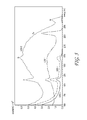
- FIG. 5 shows a low-energy ion scattering (LEIS) spectrum of the varies copper and dielectric samples. Disilane and WF 6 were provided in each cycle.
- a curve marked with LEIS1 represents 2 cycles on a Cu surface.
- a curve marked with LEIS2 represents 100 cycles on a Cu surface. It can be seen from the LEIS2 spectrum that the Cu surface is fully covered by W as indicated by the peak at about 2675 eV.
- a curve marked with LEIS3 represents 100 cycles on a low-K 2.3 surface.
- a curve marked with LEIS4 represents 100 cycles on a low-K 3.0 surface.
- the peaks at energy values of about 2675 eV represent the W peak and the peak total area corresponds to the amount of W in the surface of the sample. With the scale of FIG.
- the curves for LEIS1, LEIS3, and LEIS4 do not show significant peaks for W. It can be calculated from the peak areas in the spectrums that the selectivity of the W process applied to Cu vs. low-K 2.3 is at least about 98% and at least about 92% in the case of Cu vs. low-K 3.0.
- FIG. 6A A sample comprising copper lines embedded in a low-k material (ELK 2.3) was provided. Tungsten was selectively deposited on the copper, as shown in the TEM in FIG. 6A . In contrast, the control ( FIG. 6B ) shows no tungsten deposited over the copper. A magnification of the image of FIG. 6A is provided in FIG. 7 , showing the thickness of the W selectively deposited on the top of the Cu line.
- Tungsten was selectively deposited on a substrate comprising copper lines in a low-k material.
- a passivation removal step was carried out in which the substrate was treated consecutively with Ar plasma, Ar+H 2 plasma and with Ar+H 2 +N 2 plasma for a total of 30 seconds without interruption. Plasma was generated at 100 W power at 100° C. Ar was flowed at 1200 sccm, H 2 at 50 sccm and N 2 at 18 sccm.
- a dielectric surface restoration step was carried out.
- the substrate was treated with Si 2 H 6 for 5 seconds, which is believed, without being bound to any theory, to prevent the oxidation of the of the surfaces of the copper line and not necessarily to restore the surfaces.
- the flow rate of the Si 2 H 6 was 42 sccm.
- the substrate was transpored to a different module under nitrogen with some O 2 at 760 torr.
- Tungsten was then selectively deposited on the copper lines relative to the low-k material using alternating and sequential pulses of WF 6 and disilane, generally as described above. Deposition continued for 30 cycles at a temperature of about 130° C. A selectivity of greater than 95% was observed given a W thickness of less than 10 nm (about 8 nm nominal thickness). An SEM image of the selectively grown W on Cu is shown in FIG. 8 .
Landscapes
- Chemical & Material Sciences (AREA)
- Engineering & Computer Science (AREA)
- Physics & Mathematics (AREA)
- Chemical Kinetics & Catalysis (AREA)
- General Chemical & Material Sciences (AREA)
- Computer Hardware Design (AREA)
- Condensed Matter Physics & Semiconductors (AREA)
- Power Engineering (AREA)
- Microelectronics & Electronic Packaging (AREA)
- General Physics & Mathematics (AREA)
- Mechanical Engineering (AREA)
- Materials Engineering (AREA)
- Manufacturing & Machinery (AREA)
- Metallurgy (AREA)
- Organic Chemistry (AREA)
- Plasma & Fusion (AREA)
- Electromagnetism (AREA)
- Chemical Vapour Deposition (AREA)
- Electrodes Of Semiconductors (AREA)
- Internal Circuitry In Semiconductor Integrated Circuit Devices (AREA)
- Crystallography & Structural Chemistry (AREA)
Abstract
Metallic layers can be selectively deposited on one surface of a substrate relative to a second surface of the substrate. In some embodiments, the metallic layers are selectively deposited on copper instead of insulating or dielectric materials. In some embodiments, a first precursor forms a layer on the first surface and is subsequently reacted or converted to form a metallic layer. The deposition temperature may be selected such that a selectivity of above about 50% or even about 90% is achieved.
Description
The present application is a continuation of U.S. application Ser. No. 14/737,293, filed Jun. 11, 2015, which is a continuation of U.S. application Ser. No. 13/708,863, filed Dec. 7, 2012, now U.S. Pat. No. 9,112,003, which claims priority to U.S. Provisional Application No. 61/569,142, filed Dec. 9, 2011, each of which is hereby incorporated by reference in its entirety.
The present application relates generally to the field of semiconductor fabrication.
Integrated circuits are currently manufactured by an elaborate process in which various layers of materials are sequentially constructed in a predetermined arrangement on a semiconductor substrate.
Meeting the ever increasing electromigration (EM) requirement in copper interconnects is becoming more difficult as Moore's law progresses, resulting in smaller devices. As line dimensions shrink, critical void size for EM failure is also reduced, causing a sharp decrease in mean time to failure. A significant improvement in EM resistance is required to enable continued scaling.
The interface between the dielectric diffusion barrier and copper has been shown to be the main path for copper diffusion and the weakest link in resisting EM failure. The implementation of a selective metal cap has been challenging because of the difficulty in achieving good selectivity on copper versus the dielectric surface. Methods are disclosed herein for selective deposition on metal surfaces that can be used in this context to decrease electromigration.
In one aspect, methods are provided for selectively depositing a film on a substrate comprising a first metal surface and a second dielectric surface. The methods may comprise cleaning the substrate, for example to remove a passivation layer from the metal surface, followed by a plurality of deposition cycles, each comprising contacting the substrate with a first precursor comprising silicon or boron to selectively form a layer of first material comprising Si or B on the first metal surface relative to the second dielectric surface. The first material may be converted to a second metallic material by exposing the substrate to a second precursor comprising metal. In some embodiments, selectivity for deposition on the first surface relative to the second surface may be greater than about 50%, or even greater than about 90%. The deposition temperature may be, for example, less than about 150° C.
In some embodiments, at least the metal surface on the substrate is cleaned by exposure to a plasma. The plasma may, for example, comprise one or more of Ar, H, and N. In some embodiments the substrate is annealed after cleaning and prior to carrying out the one or more deposition cycles. The dielectric layer may also be treated in a dielectric restoration step after cleaning and prior to deposition. In some embodiments the dielectric restoration step comprises exposing the substrate to one or more silanes.
In some embodiments the first metal surface comprises copper. The second metallic material may comprise a metal nitride or metal silicide. In some embodiments the second metallic material comprises a transition metal, such as tungsten. The second precursor in the deposition cycles may be, for example, a metal halide.
Methods for selectively depositing a film on a substrate comprising a first copper surface and a second dielectric surface are also provided herein. The methods may comprise contacting the substrate with a plasma and subsequently conducting one or more deposition cycles, each comprising contacting the substrate with a first precursor comprising silicon or boron and contacting the substrate with a second precursor comprising a metal fluoride. The temperature of the substrate during the deposition cycles is selected such that the a film forms on the first surface with a selectivity of greater than about 90% relative to the second surface.
In some embodiments, the substrate is an integrated circuit workpiece comprising copper lines with a width of less than about 1 micrometer. The methods may also include a dielectric surface restoration step, such as contacting the substrate with Si2H6 or trimethylchlorosilane. In some embodiments, different process steps are carried out in different reaction spaces. For example, the substrate may be contacted with plasma in a first reaction chamber while deposition cycles are carried out in a second reaction chamber.
In some embodiments, methods for selectively depositing a film on a first metal surface of a substrate relative to a second dielectric surface are provided. The substrate may be cleaned prior to deposition, for example with a plasma comprising noble gas. In some embodiments the gas used in the plasma cleaning process comprises only argon. The cleaning may serve to remove a passivation layer from the first metal surface. After cleaning, a film is selectively deposited on the first metal surface relative to the second dielectric surface. The film may comprise, for example, a metal nitride or metal silicide. Selectivity for deposition on the first metal surface relative to the second dielectric surface may be greater than about 50% or even greater than 70%, 80% or 90% in some embodiments. In some embodiments, the second dielectric surface has not been treated to block deposition prior to selective deposition. Thus, in some embodiments the second dielectric surface does not comprise a blocking layer or passivation layer when the film is selectively deposited.
In some embodiments, selective deposition comprises alternately exposing the substrate to a first reactant and a second reactant, where the second reactant is different from the first reactant. The methods may also comprise a dielectric surface restoration step. For example, the dielectric surface may be contacted with one or more silanes after the cleaning and prior to deposition. In other embodiments a dielectric restoration step may be carried out after deposition. In addition, in some embodiments the substrate may be annealed after cleaning and prior to deposition, for example at about 150 to about 400° C.
In some embodiments, methods are disclosed for selective deposition of metallic films on metal or metallic materials while avoiding deposition on dielectric materials, such as a low-k material. For example, a metallic film may be deposited on copper for end of the line substrate processing. In some embodiments, metallic films are deposited on an integrated circuit workpiece comprising copper lines in dielectric material.
In some such applications, the selective deposition methods disclosed herein can be used to deposit material onto copper thereby decreasing electromigration of the copper. In some embodiments, the selective deposition is on the copper metal layers and not on dielectric materials on the substrate. Deposition on the dielectric materials in these applications is undesirable because it can decrease the effective dielectric value.
In some embodiments, the process flows described herein are used to selectively deposit metal on micrometer-scale (or smaller) features during integrated circuit fabrication. In some embodiments feature size may be less than 100 micrometers, less than 1 micrometer or less than 200 nm. In the case of selective deposition of W on Cu for interconnect applications, in some embodiments the feature size/line widths may be less than 1 micrometer, less than 200 nm, less than 100 nm, or even less than 50 nm. Of course the skilled artisan will recognize that selective deposition on larger features and in other contexts is possible using the disclosed methods.
In some embodiments, the selective deposition can avoid additional processing steps, thereby saving time and decreasing the costs associated with processing the substrates. For example, lithography will be very expensive in the future for small dimensions. With 8 or more layers of Cu metallization in the chips, the time and cost savings achievable using selective deposition are magnified because time is saved for each area of copper metallization during substrate processing. Also, the methods disclosed herein can obviate the need for dielectric diffusion barriers and other processing steps
In some embodiments the methods comprise selectively depositing a film on a substrate comprising a first metal surface and a second dielectric surface using a plurality of deposition cycles. The cycle comprises: contacting the substrate with a first precursor comprising silicon or boron to selectively form a layer of first material comprising Si or B over the first metal surface relative to the second dielectric surface; and converting the first material to a second metallic material by exposing the substrate to a second precursor comprising metal. The selective deposition involves forming a greater amount of material on the first metal surface relative to the second dielectric surface. The selectivity can be expressed as the ratio of material formed on the first surface to amount of material formed on the first and second surfaces combined. For example, if a process deposits 10 nm of W on a first copper surface and 1 nm on a second low-k surface, the process will be considered to have 90% selectivity. Preferably, the selectivity is above about 80%, more preferably above 90%, even more preferably above 95%, and most preferably about 100%. In some cases selectivity above 50% is acceptable. In some embodiments, multiple deposition cycles are used to deposit material. In some embodiments the selectively deposited film is a metallic layer. The metallic layer may be elemental metal. In some embodiments, the metallic layer can include additional elements, such as Si, B, N, and dopants. Thus, in some embodiments the metallic layer is a metal nitride or metal silicide. As used herein, “metallic” indicates that a film, reactant or other material comprises one or more metals.
Selective deposition using the methods described herein does not require treatment of the dielectric layer to block deposition thereon. As a result, in some embodiments the second dielectric surface does not comprise a passivation or blocking layer, such as a self-assembled monolayer (SAM), that would prevent the actual top surface of the second dielectric surface from being exposed to the chemicals of the deposition processes described herein. Thus, in some embodiments the film is deposited selectively on the first metal surface on a substrate which has not received treatment designed to prevent deposition of the film on the second dielectric surface, such as a blocking or passivation treatment. That is, in some embodiments selective deposition can be obtained even though deposition is not blocked on the second dielectric surface by a blocking or passivation layer. Instead, the deposition conditions are selected such that the selective deposition process will occur without the need for pretreatment of the second dielectric surface prior to deposition.
However, in some embodiments the second dielectric layer may be treated. For example, in some embodiments it is desirable to passivated the first metal surface and the second dielectric surface may be exposed to the same passivation treatment as the first metal surface. For example, in the case of Cu both the first Cu surface and the second dielectric surface may be exposed to BTA or other passivating chemical. However, no specific further treatments or exposures (besides what it may receive during transportation of the sample) are done for the second dielectric surface before a cleaning step to remove the passivation layer from the metal surface. In particular no treatment designed to block deposition of the film on the second dielectric surface need be carried out.
In some embodiments at the time of selective deposition of the film, the second dielectric surface comprises only surface groups that are naturally occurring in the low-k material, and does not comprise a significant amount of functional groups or ligands that would not naturally be present in the low-k material itself. In some embodiments no active treatment of the second dielectric surface is carried out after cleaning that would add surface groups to the second dielectric surface. In some embodiments the second dielectric surface comprises only surface groups that are naturally occurring in low-k materials, including those that could be formed during for transportation of the substrate in air, for example.
The substrate can comprise various types of materials. When manufacturing integrated circuits, the substrate typically comprises a number of thin films with varying chemical and physical properties. For example and without limitation, the substrate may comprise a dielectric layer and a metal layer. In some embodiments the substrate can comprise metal carbide. In some embodiments the substrate can comprise a conductive oxide.
Preferably the substrate has a first surface comprising a metal, referred to herein as the first metal surface. In some embodiments the first surface is essentially an elemental metal, such as Cu. In some embodiments the first surface comprises a metal nitride. In some embodiments the first surface comprises a transition metal. The transition metal can be selected from the group: Ti, V, Cr, Mn, Nb, Mo, Ru, Rh, Pd, Ag, Au, Hf, Ta, W, Re, Os, Ir and Pt. In some embodiments the first surface preferably comprises copper. In some embodiments the first surface comprises a noble metal. The noble metal can be selected from the group: Au, Pt, Ir, Pd, Os, Ag, Re, Rh, and Ru.
The second surface is preferably a dielectric surface. In some embodiments, the dielectric comprises SiO2. In some embodiments the dielectric is a porous material. In some embodiments the porous dielectric contains pores which are connected to each other, while in other embodiments the pores are not connected to each other. In some embodiments the dielectric comprises a low-k material, defined as an insulator with a dielectric value below about 4.0. In some embodiments the dielectric value of the low-k material is below about 3.5, below about 3.0, below about 2.5 and below about 2.3.
The precursors employed in the processes disclosed herein may be solid, liquid or gaseous material under standard conditions (room temperature and atmospheric pressure), provided that the precursors are in vapor phase before being conducted into the reaction chamber and contacted with the substrate surface. Plasma conditions can also be used. Thus, plasma can be formed from the vapor phase reactants or precursors in some embodiments. “Pulsing” a vaporized precursor onto the substrate means that the precursor vapor is conducted into the chamber for a limited period of time. Typically, the pulsing time is from about 0.05 to 10 seconds. However, depending on the substrate type and its surface area, the pulsing time may be even higher than 10 seconds. Pulsing times can be on the order of minutes in some cases. In some cases to ensure full saturation of reactions, the precursor might be supplied in multiple shorter pulses rather than in one longer pulse.
The mass flow rate of the precursors can also be determined by the skilled artisan. In one embodiment, for deposition on 300 mm wafers the flow rate of precursors is preferably between about 1 and 1000 sccm without limitation, more preferably between about 100 and 500 sccm.
The pressure in the reaction chamber is typically from about 0.01 to about 20 mbar, more preferably from about 1 to about 10 mbar. However, in some cases the pressure will be higher or lower than this range, as can be readily determined by the skilled artisan.
First Precursor:
In some embodiments a first precursor is provided to the substrate such that a layer is selectively formed on a first metal surface of the substrate relative to a second dielectric surface of the substrate. In some embodiments the first precursor preferably comprises silicon or boron. In some embodiments a 0.05-4 nm thick layer of Si or B is formed on the metal surface of the substrate. In some embodiments a 0.1-2 nm thick layer of Si or B is formed on the metal surface of the substrate. In some embodiments less than 1 nm of Si or B can be used. Without being bound to a theory, it is believed that the metal surface on the substrate can catalyze or assist in the adsorption or decomposition of the first precursor in comparison to the reactivity of the second surface or insulator. In some embodiments the formation of silicon or boron on the metal surface is self-limiting, such that up to a monolayer is formed upon exposure to the reactant. In some embodiments the silicon or boron source chemical can decompose on the copper or metal surface.
In some embodiments, the silicon source chemical is selected from the silane family SinH2n+2 (n is equal to or greater than 1) or the cyclic silane family SinH2n (n is equal to or greater than 3). In some embodiments the silicon source comprises silane or disilane. Most preferably the silane is disilane Si2H6 or trisilane Si3H8. In some embodiments the silicon source can be selected from silane compounds having the formula: SiHxLy, where L is a ligand selected from the groups including: alkyl, alkenyl, alkynyl, alkoxide, and amine. In some cases L is a ligand selected from the halide group: F, Cl, Br and I.
In some embodiments the first precursor comprises boron. In some embodiments the first precursor is diborane (B2H6). Diborane has similar properties to some of the silane based compounds. For example, diborane has a lower decomposition temperature than disilane but similar thermal stability to trisilane (silcore).
Other precursors comprising boron could also be used. The availability of a vast number of boron compounds makes it possible to choose one with the desired properties. In addition, it is possible to use more than one boron compound. Preferably, one or more of the following boron compounds is used:
Boranes according to formula I or formula II.
BnHn+x, (I)
BnHn+x, (I)
Wherein n is an integer from 1 to 10, preferably from 2 to 6, and x is an even integer, preferably 4, 6 or 8.
BnHm (II)
BnHm (II)
Wherein n is an integer from 1 to 10, preferably form 2 to 6, and m is an integer different than n, from 1 to 10, preferably from 2 to 6.
Of the above boranes according to formula I, examples include nido-boranes (BnHn+4), arachno-boranes (BnHn+6) and hyph-boranes (BnHn+8). Of the boranes according to formula II, examples include conjuncto-boranes (BnHm). Also, borane complexes such as (CH3CH2)3N—BH3 can be used.
Borane halides, particularly fluorides, bromides and chlorides. An example of a suitable compound is B2H5Br. Further examples comprise boron halides with a high boron/halide ratio, such as B2F4, B2Cl4 and B2Br4. It is also possible to use borane halide complexes.
Halogenoboranes according to formula III.
BnXn (III)
BnXn (III)
Wherein X is Cl or Br and n is 4 or an integer from 8 to 12 when X is Cl, or n is an integer from 7 to 10 when X is Br.
Carboranes according to formula IV.
C2BnHn+x (IV)
C2BnHn+x (IV)
Wherein n is an integer from 1 to 10, preferably from 2 to 6, and x is an even integer, preferably 2, 4 or 6.
Examples of carboranes according toformula IV include closo-carboranes (C2BnHn+2), nido-carboranes (C2BnHn+4) and arachno-carboranes (C2BnHn+6).
Amine-borane adducts according to formula V.
R3NBX3 (V)
R3NBX3 (V)
Wherein R is linear or branched C1 to C10, preferably C1 to C4 alkyl or H, and X is linear or branched C1 to C10, preferably C1 to C4 alkyl, H or halogen.
Aminoboranes where one or more of the substituents on B is an amino group according to formula VI.
R2N (VI)
R2N (VI)
Wherein R is linear or branched C1 to C10, preferably C1 to C4 alkyl or substituted or unsubstituted aryl group.
An example of a suitable aminoborane is (CH3)2NB(CH3)2.
Cyclic borazine (—BH—NH—)3 and its volatile derivatives.
Alkyl borons or alkyl boranes, wherein the alkyl is typically linear or branched C1 to C10 alkyl, preferably C2 to C4 alkyl.
In some embodiments the first precursor comprises germanium. In some embodiments, the germanium source chemical is selected from the germane family GenH2n+2 (n is equal to or greater than 1) or the cyclic germane family GenH2n (n is equal to or greater than 3). In some preferred embodiments the germanium source comprises germane GeH4. In some embodiments the germanium source can be selected from germane compounds having the formula: GeHxLy, where L is a ligand selected from the groups including: alkyl, alkenyl, alkynyl, alkoxide, and amine. In some cases L is a ligand selected from the halide group: F, Cl, Br and I.
Metal Source Chemicals
Preferably the second reactant comprises a metal. In some embodiments the metal is a transition metal. The transition metal can be selected from the group of: Ti, V, Cr, Mn, Nb, Mo, Ru, Rh, Pd, Ag, Hf, Ta, W, Re, Os, Ir and Pt. In some embodiments the second reactant comprises W, Ta, Nb, Ti, Mo or V. In some embodiments the second reactant preferably comprises tungsten.
In some embodiments the second reactant comprises a noble metal. The noble metal can be selected from the group: Au, Pt, Ir, Pd, Os, Ag, Rh, and Ru.
In some embodiments the second reactant comprises a metal halide (F, Cl, Br, I). In some preferred embodiments the second reactant comprises a transition metal halide. In some embodiments the second reactant preferably comprises fluorine. In some embodiments, the second reactant comprises WF6, TaF5, NbF5, TiF4, MoFx, VFx. In some embodiments the second reactant comprises WF6.
The second reactant can be used to form a variety of different materials on the substrate. In some embodiments the second reactant reacts with the first reactant on the substrate to form a metallic material on the substrate. Any of the metals disclosed above for the second reactant can be in the film deposited on the substrate.
In some embodiments an elemental metal film can be formed. In some embodiments a metal nitride film can be formed. In some embodiments a metal silicide film can be formed.
In some embodiments a metallic or elemental metal film is first formed through reaction of the Si or B on the substrate surface and the second reactant and later converted to a corresponding metal silicide or metal nitride through further processing. For example, the first metallic or elemental metal film may be exposed to a third reactant to convert it to a metal silicide or metal nitride.
In some embodiments further processing of the metallic material can be done to dope the metallic material or convert the metallic material to a metal nitride or metal silicide. In some embodiments, for example, the material can be converted to a corresponding metal nitride using plasma or a NH3-treatment. In some embodiments an electrically conductive metallic material can be converted to a more electrically resistive material or to a dielectric material by using different treatments and depending on the starting metallic material.
In some embodiments multiple pulses of one of the reactants can be provided prior to providing the next reactant. In some embodiments, any excess reactants can be removed prior to the provision of the next reactant. In some embodiments the process chamber can be purged prior to provision of the next reactant.
In some embodiments vapor phase precursors can be provided to the reaction space with the aid of an inert carrier gas. Removing excess reactants can include evacuating some of the contents of the reaction space or purging the reaction space with helium, nitrogen or any other inert gas. In some embodiments purging can comprise turning off the flow of the reactive gas while continuing to flow an inert carrier gas to the reaction space.
Deposition Temperature:
In some embodiments the temperature is selected to facilitate the selective deposition. Deposition is generally defined as selective if the amount of the deposited material per surface area or volume (e.g. at/cm2 or at/cm3) on the first surface is greater than the amount of the deposited material per surface area or volume on the second surface. The amount of material deposited on the surfaces can be determined by measuring the thicknesses of each layer. In some cases, the thickness measurement might not be possible due to non-continuous film. In some cases the selectivity can be determined by measuring the deposited atoms per surface area or volume. As mentioned above, the selectivity can be expressed as the ratio of material formed on the first surface to amount of material formed on the first and second surfaces combined. Preferably, the selectivity is above about 70%, above about 80%, more preferably above 90%, even more preferably above 95%, and most preferably about 100%. In some cases selectivity above 50% is acceptable.
In some embodiments the deposition temperature is selected such that the selectivity is above about 90%. In some embodiments, the deposition temperature is selected such that a selectivity of about 100% is achieved.
In some embodiments, the deposition temperature is selected such that the first precursor comprising silicon or boron forms a layer containing silicon or boron on the first metal surface. In some embodiments the first precursor does not form a layer on the second low-k surface, or forms a less than a complete layer on the second surface.
The particular temperature utilized can depend, in part, on the silicon or boron precursor that is selected along with the first surface or metal and the second surface or dielectric on the substrate. Preferably, the silicon or boron source forms on the first metal surface instead of the second dielectric surface to form a layer comprising silicon or boron. Preferably, the layer comprising silicon or boron is about a monolayer or less. In some cases, more than a monolayer of silicon or boron can be formed. In some embodiments a 0.05-4 nm thick layer of silicon or boron is formed on the metal surface of the substrate. In some embodiments preferably a 0.1-2 nm thick layer of silicon or boron is formed on the metal surface of the substrate. In some embodiments the formation of silicon or boron on the metal surface is self-limiting. In some embodiments the layer comprising silicon or boron is formed by decomposition.
In some cases the silicon or boron layer can form on both the metal and dielectric surfaces at higher temperatures. In such situations, the use of lower temperatures is preferred because the silicon or boron can form on the metal surface at a lower temperature than the dielectric surface. Thus, the temperature can be selected such that the silicon precursor interacts preferentially with the first surface or metal surface relative to the second surface or dielectric surface.
In some embodiments deposition temperatures are selected to achieve the desired level of selectivity. For example, a temperature can be selected such that absorption of the silicon or boron containing precursor to the low-k material is limited to an amount necessary to achieve a desired level of selectivity.
The deposition temperature can be selected based on the silicon or boron source and the particular substrate surfaces that are used (e.g. low k surface and copper surface).
In some embodiments the deposition temperature is preferably less than 200° C., more preferably less than about 175° C., and most preferably less than about 150° C. In some cases temperatures of less than about 100° C. can be used. However, at temperatures below about 100° C. a careful dosing of the precursors and optimization of the process may be used to achieve uniform films. In some embodiments the deposition temperature range for selective deposition having selectivity of over 50% in films having thicknesses of less than about 5 nm (e.g. W thickness) deposited using disilane and WF6 is from about 50° C. to about 200° C. In some embodiments desirable levels of uniformity and selectivity can be achieved using deposition temperature ranges from about 100° C. to about 150° C. In these temperature ranges a person skilled in the art can optimize the process to achieve desired or acceptable uniformity and selectivity for the films deposited using a particular reactor with particular precursors.
In some embodiments the silicon or boron-containing precursor and the second metal precursor are provided at the same temperature and in the same reaction space. In some embodiments the silicon precursor is provided at a first deposition temperature and the second metal reactant is provided at a second deposition temperature. In practice, this may mean providing the first reactant in a first reaction space and providing the second metal reactant in a second reaction space.
In one embodiment, when using a silicon containing precursor, such as disilane, and depositing on a copper surface a selectivity of more than about 90% relative to a dielectric surface can be achieved with a deposition temperature of about 130° C., for example about 130±15° C. In some embodiments, when using a silicon containing precursor, such as disilane, and depositing tungsten on a copper surface a selectivity of more than about 80% relative to a dielectric surface can be achieved, for example using a deposition temperature from about 100 to about 150° C. In some embodiments, when using a silicon containing precursor, such as disilane, and depositing on a copper surface a selectivity of more than about 50% relative to a dielectric surface can be achieved with a deposition temperature from about 80 to about 175° C. In other embodiments using disilane and depositing on a copper surface, a selectivity of more than about 95% relative to a dielectric can be achieved with a deposition temperature of below about 160° C. In other embodiments using disilane and depositing tungsten using WF6 on a copper surface, a selectivity of more than about 80%, preferably more than about 90%, relative to a dielectric can be achieved with a deposition temperature of below about 150° C. In some such embodiments the deposition temperature may be below about 140° C., 130° C. or 120° C. The deposition temperature for trisilane can be even lower than the deposition temperature for disilane. In the above mentioned embodiments the deposited film may be, for example and without limitation, a tungsten film.
In some embodiments the thickness of the film that is selectively deposited is less than about 10 nm, less than about 5 nm, about 4 nm or less or, in some embodiments, from about 1 nm to about 4 nm. However, in some cases a desired level of selectivity, for example more than 50%, more preferably more than 80%, is achieved with the thicknesses of the selectively deposited film being over about 10 nm.
In some embodiments a W film having a thickness of about 10 nm or less is deposited selectively over Cu on a substrate surface with a selectivity of greater than 50% relative to a low-k dielectric material.
In some embodiments a W film having a thickness of about 5 nm or less is deposited selectively over Cu on a substrate surface with a selectivity of greater than about 80% relative to a low-k dielectric material.
In some embodiments a W film having a thickness of about 3 nm or less is deposited selectively over Cu on a substrate surface with a selectivity of greater than about 90% relative to a low-k dielectric material.
If a lower selectivity is preferred the temperature can be slightly higher than the temperature for processes that achieve more than 90% selectivity.
In some embodiments, deposition conditions and/or reactants are selected such that etching of the low-k surface is avoided or minimized. For example, at higher temperatures metal fluorides can start fluorinating the Si—OH groups and in some cases they can etch the low-k. Thus in some embodiments the deposition temperature is selected so that etching of the low-k dielectric is avoided or eliminated.
The substrate temperature during the provision of the second reactant can be the same as the temperature during the provision of the silicon or boron containing reactant. In other embodiments, different temperatures may be used.
In embodiments where WF6 is used as the second reactant with disilane as the first reactant a temperature of about 150° C. can be used.
In some embodiments, the temperature of the substrate can be increased when providing the second reactant to increase the conversion of the metal reactant. For example, a higher temperature can be used when TaF5 and NbF5 are used as the second reactant. For example, when using TaF5 the temperatures can be over about 300° C. When using NbF5 the temperature can be above about 250° C. This can be accomplished by heating the substrate, using a higher reaction temperature for the second material or other means known to the skilled artisan.
Surface Cleaning
In some embodiments the substrate surface is cleaned prior to beginning the deposition process. For example, for embodiments when the first material is copper, the copper surface can be cleaned or reduced such that pure elemental copper is on the substrate surface. An example of an embodiment in which a copper surface is cleaned prior to deposition is illustrated at step 12 in FIG. 1 .
The cleaning step can be done in any of a variety of methods, for example using a chemical such as citric acid or plasma. For example, the substrate surface may be cleaned using hydrogen containing plasma or radicals, such as H-plasma or NH3-plasma. In some embodiments HCl treatment is used as the cleaning method. Other cleaning methods are also possible. The specific cleaning method to be used in any particular case can be selected based on a variety of factors such as the materials and the deposition conditions, including, for example, the types of materials on the substrate surface.
In some cases a first material on which selective deposition is desired, such as copper, is passivated. The passivation may be the result of an intentional treatment of the substrate to form the passivation layer, or may result from the processing conditions, such as exposure to oxygen during transport of the substrate.
The surface(s) of the substrate may be passivated, for example, prior to transfer from one reaction space to another. In some embodiments the surface of the first material may be passivated against oxidation in air using any of a variety of known passivation chemicals. In some embodiments in which selective deposition on Cu is desired, the Cu surface may be passivated, for example with BTA (benzotriazole). This passivation can be removed with the cleaning methods described herein.
In some embodiments, a passivation layer, such as a passivation layer on Cu, is removed by cleaning with plasma consisting only of Ar. In other embodiments a passivation layer o is removed with Ar and H-containing plasma. In other embodiments a passivation layer is removed with Ar and H and N-containing plasma. It may be noted that instead of Ar, other noble gases, such as He, Ne, Kr or Xe could possibly be used in substantially same conditions. In some embodiments more than one type of plasma may be used. For example, one or more of Ar-containing plasma, Ar and H-containing plasma and Ar, H and N-containing plasma may be provided. In some embodiments all three types of plasma are provided consecutively.
In some embodiments utilizing Ar-containing plasma, Ar may be provided, for example, from about 1 to about 3000 sccm, more preferably from about 300 to about 1500 sccm, and most preferably from about 1000 to about 1300 sccm. In some embodiments utilizing H-containing plasma, H2 may be provided, for example, from about 1 to about 500 sccm, more preferably from about 10 to about 200 sccm, and most preferably from about 30 to about 100 sccm. In some embodiments utilizing N-containing plasma, N2 may be provided, for example, at about from about 1 to about 500 sccm, more preferably from about 5 to about 200 sccm, and most preferably from about 5 to about 30 sccm. Similar conditions can be used for other types of plasma.
In some embodiments plasma may be generated at a power of less than about 1500 Watts, for example about 1 to about 1000 Watts, about 1 to about 500 W, or about 1 to about 200 W or less.
In some embodiments the plasma is provided for less than about 200 s, for example about 180 s or less, about 60 s or less, or about 30 s or less.
Temperature during the surface cleaning may be, for example, from about room temperature to about 150° C., or from about 100 to about 130° C.
In some embodiments, conditions for surface cleaning are selected such that etching of the low-k surface is avoided or minimized.
Dielectric Surface Treatment
In some embodiments, the dielectric material on which deposition is to be avoided can be treated prior to deposition. For example, in some embodiments the dielectric material may be treated after a surface cleaning and prior to deposition. In some embodiments, a dielectric or insulator surface can be treated to enhance the selectivity of the deposition process by decreasing the amount of material deposited on the dielectric or insulator surface. In some embodiments the treatment is intended to restore the dielectric layer and not to block deposition on the dielectric layer.
In some embodiments the dielectric or insulator surface is a low-k surface, which has been outgassed to remove moisture absorbed from the atmosphere.
In some embodiments the treatment of the dielectric or insulator is a dielectric restoration step. Different kinds of dielectric restoration steps can be performed before the selective deposition and after the surface has been cleaned (if carried out).
In some embodiments the dielectric surface is treated by contacting the dielectric surface with one or more silanes, such as disilane. In some embodiments the low-k is treated with trimethylchlorosilane (CH3)3SiCl (TMCS) or with other type of alkylhalosilanes having formula R3-xSiXx, wherein x is from 1 to 3 and each R can independently be selected to be C1-C5 hydrocarbon, such as methyl, ethyl, propyl or butyl, preferably methyl, and X is halide, preferably chloride. U.S. Pat. No. 6,391,785 discloses various surface modifications and treatments and is incorporated herein in its entirety. In some embodiments any of the surface modifications or treatments disclosed in U.S. Pat. No. 6,391,785 can be used in the methods disclosed herein.
In some embodiments, the restoration chemical is selected from the silane family and has the chemical formula SinH2n+2 (n is equal to or greater than 1), or the cyclic silane family and has the chemical formula SinH2n (n is equal to or greater than 3). In some embodiments the restoration chemical is a silicon source comprising silane or disilane. In some embodiments the silane is disilane Si2H6 or trisilane Si3H8. In some embodiments the silicon source can be selected from silane compounds having the formula: SiHxLy, where L is a ligand selected from the groups including: alkyl, alkenyl, alkynyl, alkoxide, and amine. In some cases L is a ligand selected from the halide group: F, Cl, Br and I.
In some embodiments a dielectric surface restoration step is carried out prior to selective deposition by exposing the substrate to one or more restoration chemicals, such as Si2H6 or TMCS, at a temperature of about room temperature to about 150° C., or about 100° C. to about 130° C. In some embodiments a restoration chemical, such as Si2H6, is provided to the reaction chamber at a flow rate of about 5 to 100 sccm, or about 30 to 60 sccm. In some embodiments the restoration chemical is provided to the reaction chamber for about 1 to 20 s, or about 1 to 10 s. In some embodiments a restoration chemical, such as TMCS, is provided in pulses. About 1-20 or about 1-10 pulses may be provided, for example with a pulse and purge time of about 1 to 10 seconds each.
While this step is called a surface restoration step, and the chemicals used are called restoration chemicals, these designations are used herein for simplicity and no particular restorative function is implied. Thus, in some embodiments the treatment and/or chemicals may not fully or even partially restore a dielectric surface.
If the dielectric surface is damaged, it may also be restored after selective deposition steps by conducting a surface restoration step.
Some dielectric materials can have porous structures. In order to avoid diffusion, etching, and other undesirable processes the pores can be sealed or terminated with protective groups prior to beginning the deposition process. Thus, in some embodiments a porous dielectric material can be treated to seal the pores or terminate with a protective group prior to beginning the selective deposition. In some embodiments the porous dielectric material is treated prior to providing a metal reactant.
In some embodiments the pores are sealed via silylation, i.e., forming —Si(CH3)3 groups on the low-k surface. Etching can in part be avoided by silylation prior to introducing metal fluoride or other reactants. Silylation can also be used to block the low-k pores to avoid reactant penetration into the low-k. In some embodiments silylation is accomplished through the reaction of a silicon compound, for instance Cl—Si(CH3)3, with an Si—OH terminated surface of a low-k material: Si—OH+Cl—Si(CH3)3→Si—O—Si(CH3)3+HCl. Thus, in some embodiments an appropriate surface termination is formed prior to providing the silicon compound. Also the use of silicon compounds with longer carbon containing ligands is possible.
Methods for sealing the pores are disclosed, for example, in U.S. Pat. No. 6,759,325. The disclosure of sealing methods in U.S. Pat. No. 6,759,325 is hereby incorporated by reference in its entirety.
In some embodiments an organic layer can be formed by ALD on the low-k material prior to deposition to block the pores and to make the low-k surface more resistant to metal fluorides.
In some embodiments where the selectivity is imperfect or a higher selectivity is desired, the surface can be treated after selective deposition, for example using an isotropic selective metal etch, to remove material from the insulator surface without fully removing material from the metallic surface. For example, HCl vapor or a wet etch can be used.
Exemplary Process Flows
In some embodiments, cleaning of the substrate surface 12 is followed by an optional low-k surface restoration step 17, as discussed above. For example, the low-k surface may be contacted with a silicon-containing restoration chemical, such as a silane.
In some embodiments the substrate surface is optionally further annealed in an inert atmosphere 18 after the low-k treatment step 17. The annealing is carried out at a temperature that is higher than the temperature during the cleaning step 12 or the following tungsten deposition steps 13-15. The temperature for the annealing step 18 is preferably from about 150 to about 400° C., from about 150 to about 300° C., or from about 200 to about 275° C. and in some cases at about 250° C. Without being held to any theory, it is believed that this heat treatment step may enhance the cleaning step 12, for example by enhancing the removal of any passivation chemical or layer, and thus enhance selectivity. Annealing may be carried out even if a dielectric or low-k treatment step is not conducted in a particular embodiment.
Next, a silicon or boron source is provided to the substrate, such that a silicon or boron containing species is deposited on the Cu surface 13. In some embodiments the silicon source is disilane. In some embodiments, the disilane can be selectively decomposed on the Cu surface relative to the low-k surface using a temperature at which the silicon precursor forms silicon on the copper surface but does form silicon on the hydrophobic low-k surface. In some embodiments, the silicon or boron source reacts with the copper surface in a self-limiting manner. It is believed that the Cu surface can facilitate the formation of silicon relative to the formation on the low-k surface. Silicon dioxide based surfaces like the low-k (SiOC) surfaces are not catalytically active relative to metal surfaces.
In some embodiments a 0.05-4 nm thick layer comprising silicon or boron is formed on the metal surface of the substrate in each deposition cycle. In some embodiments a 0.1-2 nm thick layer comprising silicon or boron is formed on the metal surface of the substrate in each cycle. In preferred embodiments the formation of a layer comprising silicon or boron on the metal surface is self-limiting. Thus, at most a monolayer comprising silicon or boron is formed in each cycle.
After the silicon or boron containing layer is formed on the copper layer a second reactant, such as a metal halide, is used to convert 14 the layer comprising silicon or boron to a layer comprising the corresponding metal from the second reactant, such as the metal in the metal halide. In some embodiments, WF6, TaF5, NbF5 or other compounds that are able to react with the Si or B layer are introduced to the substrate surface to form a metallic layer or metal silicide. In some embodiments, the silicon or boron precursor (e.g. disilane) and second reactant (such as metal halide) pulses can be repeated 15 to form a metallic layer 16 with a desired thickness. In some embodiments the metallic layer is elemental metal. In some embodiments, the metallic layer can include additional elements, such as Si, B, N, and dopants. In some embodiments the metallic layer is further treated to form a different material. For example an elemental metal layer can be treated using a third reactant to form a metal nitride or metal silicide.
The deposition cycle can be defined as providing the silicon or boron precursor and providing the second metal reactant. In some embodiments no other reactants are provided in the deposition cycle. In some embodiments the deposition cycle is repeated to form a metallic layer with a desired thickness. In some embodiments a 0.05-4 nm thick metallic layer is formed in each cycle. In some embodiments, preferably a 0.1-2 nm thick metallic layer is formed in each cycle. In some embodiments the metallic layer has a thickness of 1-2 nm. In other embodiments the thickness of the deposited metallic layer is above about 2 nm, in some cases above about 30 nm, and in some cases above about 50 nm. In preferred embodiments the layer has thickness of less than 10 nm.
In some embodiments the deposition cycle is repeated 10 or more times. In some embodiments, the deposition cycle is repeated at least 50 times. In some embodiments the deposition cycle is repeated about 100 times or more. The number of cycles can be selected based on the desired thickness of the metallic layer.
In some embodiments, no other reactants are provided besides the precursor comprising silicon or boron and the second metal reactant.
In some embodiments the material in the first surface, such as copper, is not converted or reacted to form another compound during the selective deposition cycle.
In some embodiments, after the one or more deposition cycles are completed a half deposition cycle can be performed. For example, a silicon or boron precursor pulse or alternatively a second metal reactant can be provided. In some embodiments, after the one or more deposition cycles a silicon or boron precursor pulse is provided. When a silicon or boron precursor pulse (or other metal reactant) is provided, the formed material can form a sacrificial layer of silicon oxide or boron oxide (or metal oxide) when exposed to air or an oxygen containing atmosphere. The sacrificial layer can prevent the metallic material underneath the silicon oxide or boron oxide layer from oxidizing when exposed to air or an oxygen-containing atmosphere outside the reactor. The formed silicon oxide or boron oxide layer can be removed in further processing steps, for example with a single pulse of metal source chemicals described herein, preferably with WF6, TaF5, NbF5, TiF4, MoFx or VFx and more preferably with WF6.
In some embodiments the entire process flow is carried out in a single reaction chamber; for example in a single process module. However, in other embodiments the various steps are carried out in two or more reaction chambers. For example, in some embodiments the cleaning 12 and surface restoration (if used) are carried out in a first reaction chamber. If the optional heat anneal step is needed or desired, the substrate may then be transported to a second reaction chamber where the heat anneal 18 (if used) and selective deposition 13-15 are carried out. In some embodiments the anneal step 18 is carried out in a second reaction chamber, and the substrate is transported back to the first reaction chamber, or to a third reaction chamber where selective deposition 13-15 is carried out. In some embodiments the cleaning and surface restoration (if used) are carried out in first reaction chamber and the selective deposition is carried out in a second, different reaction chamber without the heat anneal step in between the cleaning and depositions step. The substrate may be cooled down for a period of time prior to transport, if required. In some embodiments, the cool down is carried out for about 0 to 30 min, or about 0 to 10 minutes, at a pressure ranging from vacuum to about 2 atm, or about 0.1 torr to about 760 torr, or about 1 torr to about 760 torr. The substrate may be transported, for example, under vacuum or in the presence of N2 (and possibly some O2) at about 1 to 1000 torr.
The following non-limiting examples illustrate certain preferred embodiments of the invention. They were carried out in an ASM Pulsar® 2000 cross-flow ALD-reactor supplied by ASM Microchemistry Oy, Espoo.
To selectively deposit a metallic layer on a metal surface, for example, the surface is preferably very clean. The cleaning may be conducted via gas or liquid phase. Specifically for copper, citric acid or some other later-generation cleaning agents may be used in the liquid phase to remove the commonly employed benzotriazole (BTA) passivating agent from the surface. Alternatively, NH3 or N2/H2 containing plasma may be used as a gas phase approach to remove the BTA layer. Finally, H-radicals are used to ensure the surface is void of any oxidized copper.
Next, the silicon layer is converted to a metallic layer by exposing it to a metal fluoride (second reaction step). Suitable fluorides are, for example, WF6, NbF5, and TaF5. Of these, WF6 is reactive enough to undergo the reaction at 150° C. In the case of other metal fluorides, elevated temperatures may be required for the second reaction step. As illustrated, in FIG. 3 the WF6 reacts with the deposited silicon to form SiF4 which leaves the substrate surface and deposits tungsten. After this step, the film deposition has completed a full cycle, an additional cycle can continue with the first step, if desired. Continuing with more deposition cycles will produce a thicker metal layer 36 on the metallic substrate. The selectivity will be retained and no film will be deposited on two variants of a low-k SiO2: Low-K 3.0 and Low-K 2.3.
A copper piece was cut and cleaned with citric acid. The citric acid solution was prepared by mixing approximately 5 g of citric acid crystals in 50 ml of water. The solution was stirred until all crystals had dissolved. A fresh solution was prepared for each film deposition run and discarded immediately after use. The copper piece was dipped in the solution, left immersed for 30 seconds, and stirred a few times during that period. The copper piece was then lifted and dried by draining the liquid back into the solution. If the piece was dried by nitrogen blowing, water marks were produced. Finally, the back side of the copper piece was dried by placing the piece on a piece of clean room tissue. The cleaned copper piece was then placed onto an adapter wafer and loaded into a vacuum load lock within three minutes of cleaning.
After loading the copper piece into the vacuum load lock, it was transported by vacuum transport into the reaction chamber. The film deposition took place in an ASM Pulsar® 2000 cross-flow ALD-reactor. The temperature of the reaction chamber was 150° C. and the substrate was left to stabilize for one minute. Next, hydrogen radicals were used for the final cleaning of the copper surface to remove any oxide possibly formed after the cleaning. The overall pressure during the H-radical cleaning step was approximately 0.4 torr, and the H2 flow rate was 400 sccm. The plasma power was 125 W and the H-radical exposure time was 1.5 minutes.
Immediately after the cleaning step, the cleaned surface was exposed to a disilane pulse of 1 s, with a 2 s purge period before the following metal fluoride pulse. The flow rate of disilane was approximately 30 sccm during the pulse. This step produced a silicon layer on the copper surface. This silicon layer was then converted into a layer of metallic tungsten (W) by exposing it to WF6. The WF6 pulse length was 0.6 s with a 2 s purge. WF6 reacts with silicon to produce metallic tungsten on the surface, and volatile SiF4 as long as there is silicon remaining. As a result, a layer of W is formed, with WF6 as the surface species. If the deposition is continued with a disilane pulse, SiF4 is initially formed followed by formation of Si on the metal surface, this time facilitated by the tungsten surface. The deposition may be continued at least up to 35 nm thick layer of W while maintaining the selectivity. The overall pressure during the deposition was approximately 2.0 torr and the overall carrier gas used was purified N2.
The selectivity was retained for at least 50 nm of tungsten and no film was deposited on two variants of low-K (SiO2): Low-K 3.0 and Low-K 2.3.
A sample comprising copper lines embedded in a low-k material (ELK 2.3) was provided. Tungsten was selectively deposited on the copper, as shown in the TEM in FIG. 6A . In contrast, the control (FIG. 6B ) shows no tungsten deposited over the copper. A magnification of the image of FIG. 6A is provided in FIG. 7 , showing the thickness of the W selectively deposited on the top of the Cu line.
It will be appreciated by those skilled in the art that various modifications and changes can be made without departing from the scope of the invention. Similar other modifications and changes are intended to fall within the scope of the invention, as defined by the appended claims.
Tungsten was selectively deposited on a substrate comprising copper lines in a low-k material. A passivation removal step was carried out in which the substrate was treated consecutively with Ar plasma, Ar+H2 plasma and with Ar+H2+N2 plasma for a total of 30 seconds without interruption. Plasma was generated at 100 W power at 100° C. Ar was flowed at 1200 sccm, H2 at 50 sccm and N2 at 18 sccm.
Following the passivation removal step, a dielectric surface restoration step was carried out. The substrate was treated with Si2H6 for 5 seconds, which is believed, without being bound to any theory, to prevent the oxidation of the of the surfaces of the copper line and not necessarily to restore the surfaces. The flow rate of the Si2H6 was 42 sccm.
After cooldown for 6 minutes at 600 torr in a N2 atmosphere, the substrate was transpored to a different module under nitrogen with some O2 at 760 torr.
Tungsten was then selectively deposited on the copper lines relative to the low-k material using alternating and sequential pulses of WF6 and disilane, generally as described above. Deposition continued for 30 cycles at a temperature of about 130° C. A selectivity of greater than 95% was observed given a W thickness of less than 10 nm (about 8 nm nominal thickness). An SEM image of the selectively grown W on Cu is shown in FIG. 8 .
Claims (21)
1. A method for selectively depositing a film on a first metal surface of a substrate relative to a second dielectric surface of the substrate, the method comprising:
contacting the substrate with one or more silanes; and
carrying out one or more deposition cycles at a temperature of less than 150° C., each cycle comprising:
contacting the substrate with a first precursor comprising tungsten (W); and
contacting the substrate with a second precursor,
wherein deposition on the first metal surface relative to the second dielectric surface has a selectivity of greater than 50%.
2. The method of claim 1 , wherein at least one deposition cycle comprises contacting the substrate with the second precursor prior to contacting the substrate with the first precursor.
3. The method of claim 1 , wherein the substrate is contacted with a silane having the formula SinH2n+2, where n is equal to or greater than 1.
4. The method of claim 1 , wherein the substrate is contacted with a silane selected from silane and trisilane.
5. The method of claim 1 , wherein the substrate is contacted with disilane.
6. The method of claim 1 , wherein the substrate is contacted with a silane having the formula SiHxLy, where L is a ligand selected from alkyl, alkenyl, alkynyl, alkoxide and amide groups.
7. The method of claim 1 , wherein substrate is contacted with an alkylhalosilane having the formula R3-xSiL, wherein L is a halide, x is from 1 to 3 and each R can be independently selected from C1-C5 hydrocarbons.
8. The method of claim 7 , wherein L is chloride.
9. The method of claim 1 , wherein contacting the substrate with at least one silane forms —Si(CH3)3 groups on the second dielectric surface.
10. The method of claim 1 , wherein the substrate is contacted with one or more silanes after carrying out one or more deposition cycles.
11. The method of claim 1 , wherein the one or more deposition cycles are carried out subsequent to contacting the substrate with one or more silanes.
12. The method of claim 1 , wherein the second precursor comprises silicon or boron.
13. The method of claim 1 , wherein the first precursor comprises a tungsten halide.
14. The method of claim 1 , wherein the first precursor comprises WF6.
15. The method of claim 1 , additionally comprising cleaning the substrate prior to contacting the substrate with the one or more silanes.
16. The method of claim 15 , wherein cleaning comprises exposing the substrate to a plasma.
17. The method of claim 15 , wherein cleaning comprises removing a passivation layer from the first metal surface.
18. The method of claim 1 , wherein the first metal surface comprises copper.
19. The method of claim 1 , wherein the film comprises elemental tungsten.
20. The method of claim 1 , wherein deposition on the first metal surface relative to the second dielectric surface has a selectivity of greater than 90%.
21. The method of claim 1 , wherein contacting the substrate with one or more silanes and the deposition cycles are carried out in different reaction spaces.
Priority Applications (2)
| Application Number | Priority Date | Filing Date | Title |
|---|---|---|---|
| US15/356,306 US10157786B2 (en) | 2011-12-09 | 2016-11-18 | Selective formation of metallic films on metallic surfaces |
| US16/213,479 US11056385B2 (en) | 2011-12-09 | 2018-12-07 | Selective formation of metallic films on metallic surfaces |
Applications Claiming Priority (4)
| Application Number | Priority Date | Filing Date | Title |
|---|---|---|---|
| US201161569142P | 2011-12-09 | 2011-12-09 | |
| US13/708,863 US9112003B2 (en) | 2011-12-09 | 2012-12-07 | Selective formation of metallic films on metallic surfaces |
| US14/737,293 US9502289B2 (en) | 2011-12-09 | 2015-06-11 | Selective formation of metallic films on metallic surfaces |
| US15/356,306 US10157786B2 (en) | 2011-12-09 | 2016-11-18 | Selective formation of metallic films on metallic surfaces |
Related Parent Applications (1)
| Application Number | Title | Priority Date | Filing Date |
|---|---|---|---|
| US14/737,293 Continuation US9502289B2 (en) | 2011-12-09 | 2015-06-11 | Selective formation of metallic films on metallic surfaces |
Related Child Applications (1)
| Application Number | Title | Priority Date | Filing Date |
|---|---|---|---|
| US16/213,479 Continuation US11056385B2 (en) | 2011-12-09 | 2018-12-07 | Selective formation of metallic films on metallic surfaces |
Publications (2)
| Publication Number | Publication Date |
|---|---|
| US20170069527A1 US20170069527A1 (en) | 2017-03-09 |
| US10157786B2 true US10157786B2 (en) | 2018-12-18 |
Family
ID=48870579
Family Applications (4)
| Application Number | Title | Priority Date | Filing Date |
|---|---|---|---|
| US13/708,863 Active 2033-07-31 US9112003B2 (en) | 2011-12-09 | 2012-12-07 | Selective formation of metallic films on metallic surfaces |
| US14/737,293 Active US9502289B2 (en) | 2011-12-09 | 2015-06-11 | Selective formation of metallic films on metallic surfaces |
| US15/356,306 Active US10157786B2 (en) | 2011-12-09 | 2016-11-18 | Selective formation of metallic films on metallic surfaces |
| US16/213,479 Active US11056385B2 (en) | 2011-12-09 | 2018-12-07 | Selective formation of metallic films on metallic surfaces |
Family Applications Before (2)
| Application Number | Title | Priority Date | Filing Date |
|---|---|---|---|
| US13/708,863 Active 2033-07-31 US9112003B2 (en) | 2011-12-09 | 2012-12-07 | Selective formation of metallic films on metallic surfaces |
| US14/737,293 Active US9502289B2 (en) | 2011-12-09 | 2015-06-11 | Selective formation of metallic films on metallic surfaces |
Family Applications After (1)
| Application Number | Title | Priority Date | Filing Date |
|---|---|---|---|
| US16/213,479 Active US11056385B2 (en) | 2011-12-09 | 2018-12-07 | Selective formation of metallic films on metallic surfaces |
Country Status (1)
| Country | Link |
|---|---|
| US (4) | US9112003B2 (en) |
Cited By (29)
| Publication number | Priority date | Publication date | Assignee | Title |
|---|---|---|---|---|
| US20190157148A1 (en) * | 2017-11-17 | 2019-05-23 | Taiwan Semiconductor Manufacturing Co., Ltd. | Semiconductor structure with doped via plug and method for forming the same |
| US20190181034A1 (en) * | 2011-12-09 | 2019-06-13 | Asm International N.V. | Selective formation of metallic films on metallic surfaces |
| US10727119B2 (en) | 2017-04-26 | 2020-07-28 | Applied Materials, Inc. | Process integration approach of selective tungsten via fill |
| US10741411B2 (en) | 2015-02-23 | 2020-08-11 | Asm Ip Holding B.V. | Removal of surface passivation |
| US10793946B1 (en) | 2016-06-08 | 2020-10-06 | Asm Ip Holding B.V. | Reaction chamber passivation and selective deposition of metallic films |
| US10847361B2 (en) | 2015-08-05 | 2020-11-24 | Asm Ip Holding B.V. | Selective deposition of aluminum and nitrogen containing material |
| US10872765B2 (en) | 2018-05-02 | 2020-12-22 | Asm Ip Holding B.V. | Selective layer formation using deposition and removing |
| US10903113B2 (en) | 2015-08-05 | 2021-01-26 | Asm Ip Holding B.V. | Selective deposition of aluminum and nitrogen containing material |
| US10900120B2 (en) | 2017-07-14 | 2021-01-26 | Asm Ip Holding B.V. | Passivation against vapor deposition |
| US11047040B2 (en) | 2014-04-16 | 2021-06-29 | Asm Ip Holding B.V. | Dual selective deposition |
| US11081342B2 (en) | 2016-05-05 | 2021-08-03 | Asm Ip Holding B.V. | Selective deposition using hydrophobic precursors |
| US11094535B2 (en) | 2017-02-14 | 2021-08-17 | Asm Ip Holding B.V. | Selective passivation and selective deposition |
| US11139163B2 (en) | 2019-10-31 | 2021-10-05 | Asm Ip Holding B.V. | Selective deposition of SiOC thin films |
| US11145506B2 (en) | 2018-10-02 | 2021-10-12 | Asm Ip Holding B.V. | Selective passivation and selective deposition |
| US11170993B2 (en) | 2017-05-16 | 2021-11-09 | Asm Ip Holding B.V. | Selective PEALD of oxide on dielectric |
| US11174550B2 (en) | 2015-08-03 | 2021-11-16 | Asm Ip Holding B.V. | Selective deposition on metal or metallic surfaces relative to dielectric surfaces |
| US11213853B2 (en) | 2014-02-04 | 2022-01-04 | Asm Ip Holding B.V. | Selective deposition of metals, metal oxides, and dielectrics |
| US11387107B2 (en) | 2016-06-01 | 2022-07-12 | Asm Ip Holding B.V. | Deposition of organic films |
| US11404313B2 (en) | 2017-04-26 | 2022-08-02 | Applied Materials, Inc. | Selective tungsten deposition at low temperatures |
| US11430656B2 (en) | 2016-11-29 | 2022-08-30 | Asm Ip Holding B.V. | Deposition of oxide thin films |
| US11446699B2 (en) | 2015-10-09 | 2022-09-20 | Asm Ip Holding B.V. | Vapor phase deposition of organic films |
| US11501965B2 (en) | 2017-05-05 | 2022-11-15 | Asm Ip Holding B.V. | Plasma enhanced deposition processes for controlled formation of metal oxide thin films |
| US11608557B2 (en) | 2020-03-30 | 2023-03-21 | Asm Ip Holding B.V. | Simultaneous selective deposition of two different materials on two different surfaces |
| US11643720B2 (en) | 2020-03-30 | 2023-05-09 | Asm Ip Holding B.V. | Selective deposition of silicon oxide on metal surfaces |
| US11728175B2 (en) | 2016-06-01 | 2023-08-15 | Asm Ip Holding B.V. | Deposition of organic films |
| US11898240B2 (en) | 2020-03-30 | 2024-02-13 | Asm Ip Holding B.V. | Selective deposition of silicon oxide on dielectric surfaces relative to metal surfaces |
| US11965238B2 (en) | 2019-04-12 | 2024-04-23 | Asm Ip Holding B.V. | Selective deposition of metal oxides on metal surfaces |
| US12138654B2 (en) | 2015-10-09 | 2024-11-12 | Asm Ip Holding B.V. | Vapor phase deposition of organic films |
| US12482648B2 (en) | 2018-10-02 | 2025-11-25 | Asm Ip Holding B.V. | Selective passivation and selective deposition |
Families Citing this family (376)
| Publication number | Priority date | Publication date | Assignee | Title |
|---|---|---|---|---|
| US9394608B2 (en) | 2009-04-06 | 2016-07-19 | Asm America, Inc. | Semiconductor processing reactor and components thereof |
| JP5507909B2 (en) * | 2009-07-14 | 2014-05-28 | 東京エレクトロン株式会社 | Deposition method |
| US8802201B2 (en) | 2009-08-14 | 2014-08-12 | Asm America, Inc. | Systems and methods for thin-film deposition of metal oxides using excited nitrogen-oxygen species |
| TWI509695B (en) | 2010-06-10 | 2015-11-21 | Asm國際股份有限公司 | Method for selectively depositing a film on a substrate |
| US9312155B2 (en) | 2011-06-06 | 2016-04-12 | Asm Japan K.K. | High-throughput semiconductor-processing apparatus equipped with multiple dual-chamber modules |
| US10854498B2 (en) | 2011-07-15 | 2020-12-01 | Asm Ip Holding B.V. | Wafer-supporting device and method for producing same |
| US20130023129A1 (en) | 2011-07-20 | 2013-01-24 | Asm America, Inc. | Pressure transmitter for a semiconductor processing environment |
| US9017481B1 (en) | 2011-10-28 | 2015-04-28 | Asm America, Inc. | Process feed management for semiconductor substrate processing |
| US10714315B2 (en) | 2012-10-12 | 2020-07-14 | Asm Ip Holdings B.V. | Semiconductor reaction chamber showerhead |
| US20160376700A1 (en) | 2013-02-01 | 2016-12-29 | Asm Ip Holding B.V. | System for treatment of deposition reactor |
| US10683571B2 (en) | 2014-02-25 | 2020-06-16 | Asm Ip Holding B.V. | Gas supply manifold and method of supplying gases to chamber using same |
| US10167557B2 (en) | 2014-03-18 | 2019-01-01 | Asm Ip Holding B.V. | Gas distribution system, reactor including the system, and methods of using the same |
| US11015245B2 (en) | 2014-03-19 | 2021-05-25 | Asm Ip Holding B.V. | Gas-phase reactor and system having exhaust plenum and components thereof |
| US10858737B2 (en) | 2014-07-28 | 2020-12-08 | Asm Ip Holding B.V. | Showerhead assembly and components thereof |
| US9890456B2 (en) | 2014-08-21 | 2018-02-13 | Asm Ip Holding B.V. | Method and system for in situ formation of gas-phase compounds |
| US10941490B2 (en) | 2014-10-07 | 2021-03-09 | Asm Ip Holding B.V. | Multiple temperature range susceptor, assembly, reactor and system including the susceptor, and methods of using the same |
| US9657845B2 (en) | 2014-10-07 | 2017-05-23 | Asm Ip Holding B.V. | Variable conductance gas distribution apparatus and method |
| US10062564B2 (en) * | 2014-12-15 | 2018-08-28 | Tokyo Electron Limited | Method of selective gas phase film deposition on a substrate by modifying the surface using hydrogen plasma |
| KR102185458B1 (en) | 2015-02-03 | 2020-12-03 | 에이에스엠 아이피 홀딩 비.브이. | Selective deposition |
| US10276355B2 (en) | 2015-03-12 | 2019-04-30 | Asm Ip Holding B.V. | Multi-zone reactor, system including the reactor, and method of using the same |
| US10458018B2 (en) | 2015-06-26 | 2019-10-29 | Asm Ip Holding B.V. | Structures including metal carbide material, devices including the structures, and methods of forming same |
| US10600673B2 (en) | 2015-07-07 | 2020-03-24 | Asm Ip Holding B.V. | Magnetic susceptor to baseplate seal |
| US10343186B2 (en) | 2015-10-09 | 2019-07-09 | Asm Ip Holding B.V. | Vapor phase deposition of organic films |
| US10211308B2 (en) | 2015-10-21 | 2019-02-19 | Asm Ip Holding B.V. | NbMC layers |
| US10570514B2 (en) | 2015-11-30 | 2020-02-25 | Basf Se | Process for the generation of metallic films |
| US11139308B2 (en) | 2015-12-29 | 2021-10-05 | Asm Ip Holding B.V. | Atomic layer deposition of III-V compounds to form V-NAND devices |
| US10529554B2 (en) | 2016-02-19 | 2020-01-07 | Asm Ip Holding B.V. | Method for forming silicon nitride film selectively on sidewalls or flat surfaces of trenches |
| CN109075021B (en) | 2016-03-03 | 2023-09-05 | 应用材料公司 | Modified self-assembled monolayer barrier utilizing intermittent air-water exposure |
| US9981286B2 (en) | 2016-03-08 | 2018-05-29 | Asm Ip Holding B.V. | Selective formation of metal silicides |
| US10343920B2 (en) | 2016-03-18 | 2019-07-09 | Asm Ip Holding B.V. | Aligned carbon nanotubes |
| US10204782B2 (en) | 2016-04-18 | 2019-02-12 | Imec Vzw | Combined anneal and selective deposition process |
| KR102182550B1 (en) | 2016-04-18 | 2020-11-25 | 에이에스엠 아이피 홀딩 비.브이. | Method of forming induced self-assembly layer on a substrate |
| US10865475B2 (en) | 2016-04-21 | 2020-12-15 | Asm Ip Holding B.V. | Deposition of metal borides and silicides |
| US10190213B2 (en) | 2016-04-21 | 2019-01-29 | Asm Ip Holding B.V. | Deposition of metal borides |
| KR20180128515A (en) | 2016-04-25 | 2018-12-03 | 어플라이드 머티어리얼스, 인코포레이티드 | Chemical delivery chambers for self-assembling monolayer processes |
| US10032628B2 (en) | 2016-05-02 | 2018-07-24 | Asm Ip Holding B.V. | Source/drain performance through conformal solid state doping |
| US10367080B2 (en) | 2016-05-02 | 2019-07-30 | Asm Ip Holding B.V. | Method of forming a germanium oxynitride film |
| US11453943B2 (en) | 2016-05-25 | 2022-09-27 | Asm Ip Holding B.V. | Method for forming carbon-containing silicon/metal oxide or nitride film by ALD using silicon precursor and hydrocarbon precursor |
| US10358715B2 (en) * | 2016-06-03 | 2019-07-23 | Applied Materials, Inc. | Integrated cluster tool for selective area deposition |
| US9805974B1 (en) * | 2016-06-08 | 2017-10-31 | Asm Ip Holding B.V. | Selective deposition of metallic films |
| US10014212B2 (en) * | 2016-06-08 | 2018-07-03 | Asm Ip Holding B.V. | Selective deposition of metallic films |
| US10612137B2 (en) | 2016-07-08 | 2020-04-07 | Asm Ip Holdings B.V. | Organic reactants for atomic layer deposition |
| US9859151B1 (en) | 2016-07-08 | 2018-01-02 | Asm Ip Holding B.V. | Selective film deposition method to form air gaps |
| US10714385B2 (en) | 2016-07-19 | 2020-07-14 | Asm Ip Holding B.V. | Selective deposition of tungsten |
| KR102532607B1 (en) | 2016-07-28 | 2023-05-15 | 에이에스엠 아이피 홀딩 비.브이. | Substrate processing apparatus and method of operating the same |
| US9887082B1 (en) | 2016-07-28 | 2018-02-06 | Asm Ip Holding B.V. | Method and apparatus for filling a gap |
| US9812320B1 (en) | 2016-07-28 | 2017-11-07 | Asm Ip Holding B.V. | Method and apparatus for filling a gap |
| US10573522B2 (en) | 2016-08-16 | 2020-02-25 | Lam Research Corporation | Method for preventing line bending during metal fill process |
| TW201819665A (en) | 2016-09-10 | 2018-06-01 | 美商應用材料股份有限公司 | Selectively improved in-situ pre-cleaning for selective deposition |
| US10643826B2 (en) | 2016-10-26 | 2020-05-05 | Asm Ip Holdings B.V. | Methods for thermally calibrating reaction chambers |
| US11532757B2 (en) | 2016-10-27 | 2022-12-20 | Asm Ip Holding B.V. | Deposition of charge trapping layers |
| US10229833B2 (en) | 2016-11-01 | 2019-03-12 | Asm Ip Holding B.V. | Methods for forming a transition metal nitride film on a substrate by atomic layer deposition and related semiconductor device structures |
| US10714350B2 (en) | 2016-11-01 | 2020-07-14 | ASM IP Holdings, B.V. | Methods for forming a transition metal niobium nitride film on a substrate by atomic layer deposition and related semiconductor device structures |
| US10643904B2 (en) | 2016-11-01 | 2020-05-05 | Asm Ip Holdings B.V. | Methods for forming a semiconductor device and related semiconductor device structures |
| US10134757B2 (en) | 2016-11-07 | 2018-11-20 | Asm Ip Holding B.V. | Method of processing a substrate and a device manufactured by using the method |
| KR102546317B1 (en) | 2016-11-15 | 2023-06-21 | 에이에스엠 아이피 홀딩 비.브이. | Gas supply unit and substrate processing apparatus including the same |
| KR102762543B1 (en) | 2016-12-14 | 2025-02-05 | 에이에스엠 아이피 홀딩 비.브이. | Substrate processing apparatus |
| US11447861B2 (en) | 2016-12-15 | 2022-09-20 | Asm Ip Holding B.V. | Sequential infiltration synthesis apparatus and a method of forming a patterned structure |
| US11581186B2 (en) | 2016-12-15 | 2023-02-14 | Asm Ip Holding B.V. | Sequential infiltration synthesis apparatus |
| KR102700194B1 (en) | 2016-12-19 | 2024-08-28 | 에이에스엠 아이피 홀딩 비.브이. | Substrate processing apparatus |
| US10269558B2 (en) | 2016-12-22 | 2019-04-23 | Asm Ip Holding B.V. | Method of forming a structure on a substrate |
| US10867788B2 (en) | 2016-12-28 | 2020-12-15 | Asm Ip Holding B.V. | Method of forming a structure on a substrate |
| US11390950B2 (en) | 2017-01-10 | 2022-07-19 | Asm Ip Holding B.V. | Reactor system and method to reduce residue buildup during a film deposition process |
| TWI739984B (en) * | 2017-01-31 | 2021-09-21 | 美商應用材料股份有限公司 | Schemes for selective deposition for patterning applications |
| US10655221B2 (en) | 2017-02-09 | 2020-05-19 | Asm Ip Holding B.V. | Method for depositing oxide film by thermal ALD and PEALD |
| US10468261B2 (en) | 2017-02-15 | 2019-11-05 | Asm Ip Holding B.V. | Methods for forming a metallic film on a substrate by cyclical deposition and related semiconductor device structures |
| US10529563B2 (en) | 2017-03-29 | 2020-01-07 | Asm Ip Holdings B.V. | Method for forming doped metal oxide films on a substrate by cyclical deposition and related semiconductor device structures |
| USD876504S1 (en) | 2017-04-03 | 2020-02-25 | Asm Ip Holding B.V. | Exhaust flow control ring for semiconductor deposition apparatus |
| US10510590B2 (en) | 2017-04-10 | 2019-12-17 | Lam Research Corporation | Low resistivity films containing molybdenum |
| KR102457289B1 (en) | 2017-04-25 | 2022-10-21 | 에이에스엠 아이피 홀딩 비.브이. | Method for depositing a thin film and manufacturing a semiconductor device |
| US10892156B2 (en) | 2017-05-08 | 2021-01-12 | Asm Ip Holding B.V. | Methods for forming a silicon nitride film on a substrate and related semiconductor device structures |
| US10770286B2 (en) | 2017-05-08 | 2020-09-08 | Asm Ip Holdings B.V. | Methods for selectively forming a silicon nitride film on a substrate and related semiconductor device structures |
| KR102271771B1 (en) * | 2017-05-25 | 2021-07-01 | 삼성전자주식회사 | Method of forming thin film and method of manufacturing integrated circuit device |
| US9947582B1 (en) | 2017-06-02 | 2018-04-17 | Asm Ip Holding B.V. | Processes for preventing oxidation of metal thin films |
| TWI729285B (en) * | 2017-06-14 | 2021-06-01 | 荷蘭商Asm Ip控股公司 | Selective deposition of metallic films |
| US12040200B2 (en) | 2017-06-20 | 2024-07-16 | Asm Ip Holding B.V. | Semiconductor processing apparatus and methods for calibrating a semiconductor processing apparatus |
| US11306395B2 (en) | 2017-06-28 | 2022-04-19 | Asm Ip Holding B.V. | Methods for depositing a transition metal nitride film on a substrate by atomic layer deposition and related deposition apparatus |
| US10685834B2 (en) | 2017-07-05 | 2020-06-16 | Asm Ip Holdings B.V. | Methods for forming a silicon germanium tin layer and related semiconductor device structures |
| TWI772459B (en) | 2017-07-14 | 2022-08-01 | 荷蘭商Asm Ip控股公司 | Methods for preparing self-assembled monolayers |
| KR20190009245A (en) | 2017-07-18 | 2019-01-28 | 에이에스엠 아이피 홀딩 비.브이. | Methods for forming a semiconductor device structure and related semiconductor device structures |
| TWI722301B (en) | 2017-07-18 | 2021-03-21 | 美商應用材料股份有限公司 | Methods for depositing blocking layers on metal material surfaces |
| US11374112B2 (en) | 2017-07-19 | 2022-06-28 | Asm Ip Holding B.V. | Method for depositing a group IV semiconductor and related semiconductor device structures |
| US11018002B2 (en) | 2017-07-19 | 2021-05-25 | Asm Ip Holding B.V. | Method for selectively depositing a Group IV semiconductor and related semiconductor device structures |
| US10541333B2 (en) | 2017-07-19 | 2020-01-21 | Asm Ip Holding B.V. | Method for depositing a group IV semiconductor and related semiconductor device structures |
| US10590535B2 (en) | 2017-07-26 | 2020-03-17 | Asm Ip Holdings B.V. | Chemical treatment, deposition and/or infiltration apparatus and method for using the same |
| TWI815813B (en) | 2017-08-04 | 2023-09-21 | 荷蘭商Asm智慧財產控股公司 | Showerhead assembly for distributing a gas within a reaction chamber |
| US10692741B2 (en) | 2017-08-08 | 2020-06-23 | Asm Ip Holdings B.V. | Radiation shield |
| US10770336B2 (en) | 2017-08-08 | 2020-09-08 | Asm Ip Holding B.V. | Substrate lift mechanism and reactor including same |
| US11139191B2 (en) | 2017-08-09 | 2021-10-05 | Asm Ip Holding B.V. | Storage apparatus for storing cassettes for substrates and processing apparatus equipped therewith |
| US10249524B2 (en) | 2017-08-09 | 2019-04-02 | Asm Ip Holding B.V. | Cassette holder assembly for a substrate cassette and holding member for use in such assembly |
| US11769682B2 (en) | 2017-08-09 | 2023-09-26 | Asm Ip Holding B.V. | Storage apparatus for storing cassettes for substrates and processing apparatus equipped therewith |
| USD900036S1 (en) | 2017-08-24 | 2020-10-27 | Asm Ip Holding B.V. | Heater electrical connector and adapter |
| US11830730B2 (en) | 2017-08-29 | 2023-11-28 | Asm Ip Holding B.V. | Layer forming method and apparatus |
| KR102491945B1 (en) | 2017-08-30 | 2023-01-26 | 에이에스엠 아이피 홀딩 비.브이. | Substrate processing apparatus |
| US11295980B2 (en) | 2017-08-30 | 2022-04-05 | Asm Ip Holding B.V. | Methods for depositing a molybdenum metal film over a dielectric surface of a substrate by a cyclical deposition process and related semiconductor device structures |
| US11056344B2 (en) | 2017-08-30 | 2021-07-06 | Asm Ip Holding B.V. | Layer forming method |
| US10515896B2 (en) * | 2017-08-31 | 2019-12-24 | Taiwan Semiconductor Manufacturing Co., Ltd. | Interconnect structure for semiconductor device and methods of fabrication thereof |
| KR102401446B1 (en) | 2017-08-31 | 2022-05-24 | 에이에스엠 아이피 홀딩 비.브이. | Substrate processing apparatus |
| KR102630301B1 (en) | 2017-09-21 | 2024-01-29 | 에이에스엠 아이피 홀딩 비.브이. | Method of sequential infiltration synthesis treatment of infiltrateable material and structures and devices formed using same |
| US10844484B2 (en) | 2017-09-22 | 2020-11-24 | Asm Ip Holding B.V. | Apparatus for dispensing a vapor phase reactant to a reaction chamber and related methods |
| US10658205B2 (en) | 2017-09-28 | 2020-05-19 | Asm Ip Holdings B.V. | Chemical dispensing apparatus and methods for dispensing a chemical to a reaction chamber |
| US10403504B2 (en) | 2017-10-05 | 2019-09-03 | Asm Ip Holding B.V. | Method for selectively depositing a metallic film on a substrate |
| US10319588B2 (en) | 2017-10-10 | 2019-06-11 | Asm Ip Holding B.V. | Method for depositing a metal chalcogenide on a substrate by cyclical deposition |
| US10923344B2 (en) | 2017-10-30 | 2021-02-16 | Asm Ip Holding B.V. | Methods for forming a semiconductor structure and related semiconductor structures |
| US10892161B2 (en) | 2017-11-14 | 2021-01-12 | Applied Materials, Inc. | Enhanced selective deposition process |
| US10910262B2 (en) | 2017-11-16 | 2021-02-02 | Asm Ip Holding B.V. | Method of selectively depositing a capping layer structure on a semiconductor device structure |
| KR102443047B1 (en) | 2017-11-16 | 2022-09-14 | 에이에스엠 아이피 홀딩 비.브이. | Substrate processing apparatus method and apparatus manufactured thereby |
| TWI831756B (en) * | 2017-11-20 | 2024-02-11 | 美商蘭姆研究公司 | Method and apparatus for forming metal film |
| US11022879B2 (en) | 2017-11-24 | 2021-06-01 | Asm Ip Holding B.V. | Method of forming an enhanced unexposed photoresist layer |
| CN111344522B (en) | 2017-11-27 | 2022-04-12 | 阿斯莫Ip控股公司 | Units including clean mini environments |
| KR102597978B1 (en) | 2017-11-27 | 2023-11-06 | 에이에스엠 아이피 홀딩 비.브이. | Storage device for storing wafer cassettes for use with batch furnaces |
| SG11202005432RA (en) * | 2017-12-17 | 2020-07-29 | Applied Materials Inc | Silicide films through selective deposition |
| US10872771B2 (en) | 2018-01-16 | 2020-12-22 | Asm Ip Holding B. V. | Method for depositing a material film on a substrate within a reaction chamber by a cyclical deposition process and related device structures |
| TWI799494B (en) * | 2018-01-19 | 2023-04-21 | 荷蘭商Asm 智慧財產控股公司 | Deposition method |
| WO2019142055A2 (en) | 2018-01-19 | 2019-07-25 | Asm Ip Holding B.V. | Method for depositing a gap-fill layer by plasma-assisted deposition |
| USD903477S1 (en) | 2018-01-24 | 2020-12-01 | Asm Ip Holdings B.V. | Metal clamp |
| US11018047B2 (en) | 2018-01-25 | 2021-05-25 | Asm Ip Holding B.V. | Hybrid lift pin |
| USD880437S1 (en) | 2018-02-01 | 2020-04-07 | Asm Ip Holding B.V. | Gas supply plate for semiconductor manufacturing apparatus |
| US11081345B2 (en) | 2018-02-06 | 2021-08-03 | Asm Ip Holding B.V. | Method of post-deposition treatment for silicon oxide film |
| US10896820B2 (en) | 2018-02-14 | 2021-01-19 | Asm Ip Holding B.V. | Method for depositing a ruthenium-containing film on a substrate by a cyclical deposition process |
| US11685991B2 (en) | 2018-02-14 | 2023-06-27 | Asm Ip Holding B.V. | Method for depositing a ruthenium-containing film on a substrate by a cyclical deposition process |
| US10731249B2 (en) | 2018-02-15 | 2020-08-04 | Asm Ip Holding B.V. | Method of forming a transition metal containing film on a substrate by a cyclical deposition process, a method for supplying a transition metal halide compound to a reaction chamber, and related vapor deposition apparatus |
| KR102636427B1 (en) | 2018-02-20 | 2024-02-13 | 에이에스엠 아이피 홀딩 비.브이. | Substrate processing method and apparatus |
| US10658181B2 (en) | 2018-02-20 | 2020-05-19 | Asm Ip Holding B.V. | Method of spacer-defined direct patterning in semiconductor fabrication |
| US10975470B2 (en) | 2018-02-23 | 2021-04-13 | Asm Ip Holding B.V. | Apparatus for detecting or monitoring for a chemical precursor in a high temperature environment |
| US11473195B2 (en) | 2018-03-01 | 2022-10-18 | Asm Ip Holding B.V. | Semiconductor processing apparatus and a method for processing a substrate |
| US11404275B2 (en) | 2018-03-02 | 2022-08-02 | Lam Research Corporation | Selective deposition using hydrolysis |
| US11629406B2 (en) | 2018-03-09 | 2023-04-18 | Asm Ip Holding B.V. | Semiconductor processing apparatus comprising one or more pyrometers for measuring a temperature of a substrate during transfer of the substrate |
| US11114283B2 (en) | 2018-03-16 | 2021-09-07 | Asm Ip Holding B.V. | Reactor, system including the reactor, and methods of manufacturing and using same |
| KR102646467B1 (en) | 2018-03-27 | 2024-03-11 | 에이에스엠 아이피 홀딩 비.브이. | Method of forming an electrode on a substrate and a semiconductor device structure including an electrode |
| US11230766B2 (en) | 2018-03-29 | 2022-01-25 | Asm Ip Holding B.V. | Substrate processing apparatus and method |
| US11088002B2 (en) | 2018-03-29 | 2021-08-10 | Asm Ip Holding B.V. | Substrate rack and a substrate processing system and method |
| KR102501472B1 (en) | 2018-03-30 | 2023-02-20 | 에이에스엠 아이피 홀딩 비.브이. | Substrate processing method |
| KR102600229B1 (en) | 2018-04-09 | 2023-11-10 | 에이에스엠 아이피 홀딩 비.브이. | Substrate supporting device, substrate processing apparatus including the same and substrate processing method |
| KR102806630B1 (en) | 2018-05-03 | 2025-05-12 | 램 리써치 코포레이션 | Method for depositing tungsten and other metals on 3D NAND structures |
| US12025484B2 (en) | 2018-05-08 | 2024-07-02 | Asm Ip Holding B.V. | Thin film forming method |
| TWI811348B (en) | 2018-05-08 | 2023-08-11 | 荷蘭商Asm 智慧財產控股公司 | Methods for depositing an oxide film on a substrate by a cyclical deposition process and related device structures |
| US12272527B2 (en) | 2018-05-09 | 2025-04-08 | Asm Ip Holding B.V. | Apparatus for use with hydrogen radicals and method of using same |
| TWI816783B (en) | 2018-05-11 | 2023-10-01 | 荷蘭商Asm 智慧財產控股公司 | Methods for forming a doped metal carbide film on a substrate and related semiconductor device structures |
| KR102596988B1 (en) | 2018-05-28 | 2023-10-31 | 에이에스엠 아이피 홀딩 비.브이. | Method of processing a substrate and a device manufactured by the same |
| TWI840362B (en) | 2018-06-04 | 2024-05-01 | 荷蘭商Asm Ip私人控股有限公司 | Wafer handling chamber with moisture reduction |
| US11718913B2 (en) | 2018-06-04 | 2023-08-08 | Asm Ip Holding B.V. | Gas distribution system and reactor system including same |
| US11286562B2 (en) | 2018-06-08 | 2022-03-29 | Asm Ip Holding B.V. | Gas-phase chemical reactor and method of using same |
| KR102568797B1 (en) | 2018-06-21 | 2023-08-21 | 에이에스엠 아이피 홀딩 비.브이. | Substrate processing system |
| US10797133B2 (en) | 2018-06-21 | 2020-10-06 | Asm Ip Holding B.V. | Method for depositing a phosphorus doped silicon arsenide film and related semiconductor device structures |
| KR102854019B1 (en) | 2018-06-27 | 2025-09-02 | 에이에스엠 아이피 홀딩 비.브이. | Periodic deposition method for forming a metal-containing material and films and structures comprising the metal-containing material |
| TWI815915B (en) | 2018-06-27 | 2023-09-21 | 荷蘭商Asm Ip私人控股有限公司 | Cyclic deposition methods for forming metal-containing material and films and structures including the metal-containing material |
| US10612136B2 (en) | 2018-06-29 | 2020-04-07 | ASM IP Holding, B.V. | Temperature-controlled flange and reactor system including same |
| KR102686758B1 (en) | 2018-06-29 | 2024-07-18 | 에이에스엠 아이피 홀딩 비.브이. | Method for depositing a thin film and manufacturing a semiconductor device |
| US10755922B2 (en) | 2018-07-03 | 2020-08-25 | Asm Ip Holding B.V. | Method for depositing silicon-free carbon-containing film as gap-fill layer by pulse plasma-assisted deposition |
| US10388513B1 (en) | 2018-07-03 | 2019-08-20 | Asm Ip Holding B.V. | Method for depositing silicon-free carbon-containing film as gap-fill layer by pulse plasma-assisted deposition |
| US10767789B2 (en) | 2018-07-16 | 2020-09-08 | Asm Ip Holding B.V. | Diaphragm valves, valve components, and methods for forming valve components |
| US11053591B2 (en) | 2018-08-06 | 2021-07-06 | Asm Ip Holding B.V. | Multi-port gas injection system and reactor system including same |
| US10883175B2 (en) | 2018-08-09 | 2021-01-05 | Asm Ip Holding B.V. | Vertical furnace for processing substrates and a liner for use therein |
| US10829852B2 (en) | 2018-08-16 | 2020-11-10 | Asm Ip Holding B.V. | Gas distribution device for a wafer processing apparatus |
| US11430674B2 (en) | 2018-08-22 | 2022-08-30 | Asm Ip Holding B.V. | Sensor array, apparatus for dispensing a vapor phase reactant to a reaction chamber and related methods |
| US11024523B2 (en) | 2018-09-11 | 2021-06-01 | Asm Ip Holding B.V. | Substrate processing apparatus and method |
| KR102707956B1 (en) | 2018-09-11 | 2024-09-19 | 에이에스엠 아이피 홀딩 비.브이. | Method for deposition of a thin film |
| US11049751B2 (en) | 2018-09-14 | 2021-06-29 | Asm Ip Holding B.V. | Cassette supply system to store and handle cassettes and processing apparatus equipped therewith |
| DE102018131694B4 (en) * | 2018-09-28 | 2025-03-13 | Taiwan Semiconductor Manufacturing Co., Ltd. | METHOD FOR FORMING AN INTEGRATED CIRCUIT STRUCTURE |
| CN110970344B (en) | 2018-10-01 | 2024-10-25 | Asmip控股有限公司 | Substrate holding device, system including the same and method of using the same |
| US11232963B2 (en) | 2018-10-03 | 2022-01-25 | Asm Ip Holding B.V. | Substrate processing apparatus and method |
| KR102592699B1 (en) | 2018-10-08 | 2023-10-23 | 에이에스엠 아이피 홀딩 비.브이. | Substrate support unit and apparatuses for depositing thin film and processing the substrate including the same |
| US10847365B2 (en) | 2018-10-11 | 2020-11-24 | Asm Ip Holding B.V. | Method of forming conformal silicon carbide film by cyclic CVD |
| US10811256B2 (en) | 2018-10-16 | 2020-10-20 | Asm Ip Holding B.V. | Method for etching a carbon-containing feature |
| KR102546322B1 (en) | 2018-10-19 | 2023-06-21 | 에이에스엠 아이피 홀딩 비.브이. | Substrate processing apparatus and substrate processing method |
| KR102605121B1 (en) | 2018-10-19 | 2023-11-23 | 에이에스엠 아이피 홀딩 비.브이. | Substrate processing apparatus and substrate processing method |
| USD948463S1 (en) | 2018-10-24 | 2022-04-12 | Asm Ip Holding B.V. | Susceptor for semiconductor substrate supporting apparatus |
| US12378665B2 (en) | 2018-10-26 | 2025-08-05 | Asm Ip Holding B.V. | High temperature coatings for a preclean and etch apparatus and related methods |
| US11087997B2 (en) | 2018-10-31 | 2021-08-10 | Asm Ip Holding B.V. | Substrate processing apparatus for processing substrates |
| KR102748291B1 (en) | 2018-11-02 | 2024-12-31 | 에이에스엠 아이피 홀딩 비.브이. | Substrate support unit and substrate processing apparatus including the same |
| US11572620B2 (en) | 2018-11-06 | 2023-02-07 | Asm Ip Holding B.V. | Methods for selectively depositing an amorphous silicon film on a substrate |
| US11031242B2 (en) | 2018-11-07 | 2021-06-08 | Asm Ip Holding B.V. | Methods for depositing a boron doped silicon germanium film |
| US10818758B2 (en) | 2018-11-16 | 2020-10-27 | Asm Ip Holding B.V. | Methods for forming a metal silicate film on a substrate in a reaction chamber and related semiconductor device structures |
| US10847366B2 (en) | 2018-11-16 | 2020-11-24 | Asm Ip Holding B.V. | Methods for depositing a transition metal chalcogenide film on a substrate by a cyclical deposition process |
| KR20250116174A (en) * | 2018-11-19 | 2025-07-31 | 램 리써치 코포레이션 | Molybdenum templates for tungsten |
| US10559458B1 (en) | 2018-11-26 | 2020-02-11 | Asm Ip Holding B.V. | Method of forming oxynitride film |
| US12040199B2 (en) | 2018-11-28 | 2024-07-16 | Asm Ip Holding B.V. | Substrate processing apparatus for processing substrates |
| US11217444B2 (en) | 2018-11-30 | 2022-01-04 | Asm Ip Holding B.V. | Method for forming an ultraviolet radiation responsive metal oxide-containing film |
| KR102636428B1 (en) | 2018-12-04 | 2024-02-13 | 에이에스엠 아이피 홀딩 비.브이. | A method for cleaning a substrate processing apparatus |
| US11158513B2 (en) | 2018-12-13 | 2021-10-26 | Asm Ip Holding B.V. | Methods for forming a rhenium-containing film on a substrate by a cyclical deposition process and related semiconductor device structures |
| JP7504584B2 (en) | 2018-12-14 | 2024-06-24 | エーエスエム・アイピー・ホールディング・ベー・フェー | Method and system for forming device structures using selective deposition of gallium nitride - Patents.com |
| KR102857307B1 (en) | 2018-12-14 | 2025-09-08 | 램 리써치 코포레이션 | Atomic layer deposition on 3D NAND structures |
| TWI819180B (en) | 2019-01-17 | 2023-10-21 | 荷蘭商Asm 智慧財產控股公司 | Methods of forming a transition metal containing film on a substrate by a cyclical deposition process |
| KR102727227B1 (en) | 2019-01-22 | 2024-11-07 | 에이에스엠 아이피 홀딩 비.브이. | Semiconductor processing device |
| SG11202108217UA (en) | 2019-01-28 | 2021-08-30 | Lam Res Corp | Deposition of metal films |
| CN111524788B (en) | 2019-02-01 | 2023-11-24 | Asm Ip私人控股有限公司 | Method for forming topologically selective films of silicon oxide |
| TWI845607B (en) | 2019-02-20 | 2024-06-21 | 荷蘭商Asm Ip私人控股有限公司 | Cyclical deposition method and apparatus for filling a recess formed within a substrate surface |
| US11482533B2 (en) | 2019-02-20 | 2022-10-25 | Asm Ip Holding B.V. | Apparatus and methods for plug fill deposition in 3-D NAND applications |
| KR102626263B1 (en) | 2019-02-20 | 2024-01-16 | 에이에스엠 아이피 홀딩 비.브이. | Cyclical deposition method including treatment step and apparatus for same |
| JP7603377B2 (en) | 2019-02-20 | 2024-12-20 | エーエスエム・アイピー・ホールディング・ベー・フェー | Method and apparatus for filling recesses formed in a substrate surface - Patents.com |
| TWI842826B (en) | 2019-02-22 | 2024-05-21 | 荷蘭商Asm Ip私人控股有限公司 | Substrate processing apparatus and method for processing substrate |
| KR102762833B1 (en) | 2019-03-08 | 2025-02-04 | 에이에스엠 아이피 홀딩 비.브이. | STRUCTURE INCLUDING SiOCN LAYER AND METHOD OF FORMING SAME |
| KR102782593B1 (en) | 2019-03-08 | 2025-03-14 | 에이에스엠 아이피 홀딩 비.브이. | Structure Including SiOC Layer and Method of Forming Same |
| KR102858005B1 (en) | 2019-03-08 | 2025-09-09 | 에이에스엠 아이피 홀딩 비.브이. | Method for Selective Deposition of Silicon Nitride Layer and Structure Including Selectively-Deposited Silicon Nitride Layer |
| CN113557320B (en) | 2019-03-11 | 2024-08-27 | 朗姆研究公司 | Precursors for depositing molybdenum-containing films |
| JP2020167398A (en) | 2019-03-28 | 2020-10-08 | エーエスエム・アイピー・ホールディング・ベー・フェー | Door openers and substrate processing equipment provided with door openers |
| KR102809999B1 (en) | 2019-04-01 | 2025-05-19 | 에이에스엠 아이피 홀딩 비.브이. | Method of manufacturing semiconductor device |
| WO2020210260A1 (en) | 2019-04-11 | 2020-10-15 | Lam Research Corporation | High step coverage tungsten deposition |
| KR102897355B1 (en) | 2019-04-19 | 2025-12-08 | 에이에스엠 아이피 홀딩 비.브이. | Layer forming method and apparatus |
| KR20200125453A (en) | 2019-04-24 | 2020-11-04 | 에이에스엠 아이피 홀딩 비.브이. | Gas-phase reactor system and method of using same |
| KR20200130121A (en) | 2019-05-07 | 2020-11-18 | 에이에스엠 아이피 홀딩 비.브이. | Chemical source vessel with dip tube |
| KR102869364B1 (en) | 2019-05-07 | 2025-10-10 | 에이에스엠 아이피 홀딩 비.브이. | Method for Reforming Amorphous Carbon Polymer Film |
| KR20200130652A (en) | 2019-05-10 | 2020-11-19 | 에이에스엠 아이피 홀딩 비.브이. | Method of depositing material onto a surface and structure formed according to the method |
| JP7612342B2 (en) | 2019-05-16 | 2025-01-14 | エーエスエム・アイピー・ホールディング・ベー・フェー | Wafer boat handling apparatus, vertical batch furnace and method |
| JP7598201B2 (en) | 2019-05-16 | 2024-12-11 | エーエスエム・アイピー・ホールディング・ベー・フェー | Wafer boat handling apparatus, vertical batch furnace and method |
| USD947913S1 (en) | 2019-05-17 | 2022-04-05 | Asm Ip Holding B.V. | Susceptor shaft |
| USD975665S1 (en) | 2019-05-17 | 2023-01-17 | Asm Ip Holding B.V. | Susceptor shaft |
| CN113874545A (en) * | 2019-05-22 | 2021-12-31 | 朗姆研究公司 | Nucleation-free tungsten deposition |
| USD935572S1 (en) | 2019-05-24 | 2021-11-09 | Asm Ip Holding B.V. | Gas channel plate |
| USD922229S1 (en) | 2019-06-05 | 2021-06-15 | Asm Ip Holding B.V. | Device for controlling a temperature of a gas supply unit |
| KR20200141002A (en) | 2019-06-06 | 2020-12-17 | 에이에스엠 아이피 홀딩 비.브이. | Method of using a gas-phase reactor system including analyzing exhausted gas |
| US12252785B2 (en) | 2019-06-10 | 2025-03-18 | Asm Ip Holding B.V. | Method for cleaning quartz epitaxial chambers |
| KR20200143254A (en) | 2019-06-11 | 2020-12-23 | 에이에스엠 아이피 홀딩 비.브이. | Method of forming an electronic structure using an reforming gas, system for performing the method, and structure formed using the method |
| USD944946S1 (en) | 2019-06-14 | 2022-03-01 | Asm Ip Holding B.V. | Shower plate |
| USD931978S1 (en) | 2019-06-27 | 2021-09-28 | Asm Ip Holding B.V. | Showerhead vacuum transport |
| KR102911421B1 (en) | 2019-07-03 | 2026-01-12 | 에이에스엠 아이피 홀딩 비.브이. | Temperature control assembly for substrate processing apparatus and method of using same |
| JP7499079B2 (en) | 2019-07-09 | 2024-06-13 | エーエスエム・アイピー・ホールディング・ベー・フェー | Plasma device using coaxial waveguide and substrate processing method |
| KR20210008310A (en) | 2019-07-10 | 2021-01-21 | 에이에스엠 아이피 홀딩 비.브이. | Substrate supporting assembly and substrate processing apparatus comprising the same |
| KR102895115B1 (en) | 2019-07-16 | 2025-12-03 | 에이에스엠 아이피 홀딩 비.브이. | Substrate processing apparatus |
| KR102860110B1 (en) | 2019-07-17 | 2025-09-16 | 에이에스엠 아이피 홀딩 비.브이. | Methods of forming silicon germanium structures |
| KR20210010816A (en) | 2019-07-17 | 2021-01-28 | 에이에스엠 아이피 홀딩 비.브이. | Radical assist ignition plasma system and method |
| US11643724B2 (en) | 2019-07-18 | 2023-05-09 | Asm Ip Holding B.V. | Method of forming structures using a neutral beam |
| KR102903090B1 (en) | 2019-07-19 | 2025-12-19 | 에이에스엠 아이피 홀딩 비.브이. | Method of Forming Topology-Controlled Amorphous Carbon Polymer Film |
| TWI839544B (en) | 2019-07-19 | 2024-04-21 | 荷蘭商Asm Ip私人控股有限公司 | Method of forming topology-controlled amorphous carbon polymer film |
| TWI851767B (en) | 2019-07-29 | 2024-08-11 | 荷蘭商Asm Ip私人控股有限公司 | Methods for selective deposition utilizing n-type dopants and/or alternative dopants to achieve high dopant incorporation |
| KR20210015655A (en) | 2019-07-30 | 2021-02-10 | 에이에스엠 아이피 홀딩 비.브이. | Substrate processing apparatus and method |
| CN112309899B (en) | 2019-07-30 | 2025-11-14 | Asmip私人控股有限公司 | Substrate processing equipment |
| CN112309900B (en) | 2019-07-30 | 2025-11-04 | Asmip私人控股有限公司 | Substrate processing equipment |
| US11587815B2 (en) | 2019-07-31 | 2023-02-21 | Asm Ip Holding B.V. | Vertical batch furnace assembly |
| US11227782B2 (en) | 2019-07-31 | 2022-01-18 | Asm Ip Holding B.V. | Vertical batch furnace assembly |
| US11587814B2 (en) | 2019-07-31 | 2023-02-21 | Asm Ip Holding B.V. | Vertical batch furnace assembly |
| KR20210018759A (en) | 2019-08-05 | 2021-02-18 | 에이에스엠 아이피 홀딩 비.브이. | Liquid level sensor for a chemical source vessel |
| CN112342526A (en) | 2019-08-09 | 2021-02-09 | Asm Ip私人控股有限公司 | Heater assembly including cooling device and method of using same |
| CN114269963A (en) | 2019-08-12 | 2022-04-01 | 朗姆研究公司 | Tungsten deposition |
| USD965044S1 (en) | 2019-08-19 | 2022-09-27 | Asm Ip Holding B.V. | Susceptor shaft |
| USD965524S1 (en) | 2019-08-19 | 2022-10-04 | Asm Ip Holding B.V. | Susceptor support |
| US11639548B2 (en) | 2019-08-21 | 2023-05-02 | Asm Ip Holding B.V. | Film-forming material mixed-gas forming device and film forming device |
| KR20210024423A (en) | 2019-08-22 | 2021-03-05 | 에이에스엠 아이피 홀딩 비.브이. | Method for forming a structure with a hole |
| USD930782S1 (en) | 2019-08-22 | 2021-09-14 | Asm Ip Holding B.V. | Gas distributor |
| USD940837S1 (en) | 2019-08-22 | 2022-01-11 | Asm Ip Holding B.V. | Electrode |
| USD949319S1 (en) | 2019-08-22 | 2022-04-19 | Asm Ip Holding B.V. | Exhaust duct |
| USD979506S1 (en) | 2019-08-22 | 2023-02-28 | Asm Ip Holding B.V. | Insulator |
| TWI838570B (en) | 2019-08-23 | 2024-04-11 | 荷蘭商Asm Ip私人控股有限公司 | Method for depositing silicon oxide film having improved quality by peald using bis(diethylamino)silane |
| US11286558B2 (en) | 2019-08-23 | 2022-03-29 | Asm Ip Holding B.V. | Methods for depositing a molybdenum nitride film on a surface of a substrate by a cyclical deposition process and related semiconductor device structures including a molybdenum nitride film |
| JP2022546404A (en) | 2019-08-28 | 2022-11-04 | ラム リサーチ コーポレーション | deposition of metal |
| KR102778456B1 (en) | 2019-08-29 | 2025-03-12 | 삼성전자주식회사 | Semiconductor device and method of fabricating the same |
| KR102868968B1 (en) | 2019-09-03 | 2025-10-10 | 에이에스엠 아이피 홀딩 비.브이. | Methods and apparatus for depositing a chalcogenide film and structures including the film |
| US12334351B2 (en) | 2019-09-03 | 2025-06-17 | Lam Research Corporation | Molybdenum deposition |
| KR102806450B1 (en) | 2019-09-04 | 2025-05-12 | 에이에스엠 아이피 홀딩 비.브이. | Methods for selective deposition using a sacrificial capping layer |
| KR102733104B1 (en) | 2019-09-05 | 2024-11-22 | 에이에스엠 아이피 홀딩 비.브이. | Substrate processing apparatus |
| US11094588B2 (en) | 2019-09-05 | 2021-08-17 | Applied Materials, Inc. | Interconnection structure of selective deposition process |
| US12469693B2 (en) | 2019-09-17 | 2025-11-11 | Asm Ip Holding B.V. | Method of forming a carbon-containing layer and structure including the layer |
| US11469139B2 (en) | 2019-09-20 | 2022-10-11 | Taiwan Semiconductor Manufacturing Company, Ltd. | Bottom-up formation of contact plugs |
| US11562901B2 (en) | 2019-09-25 | 2023-01-24 | Asm Ip Holding B.V. | Substrate processing method |
| CN112593212B (en) | 2019-10-02 | 2023-12-22 | Asm Ip私人控股有限公司 | Method for forming topologically selective silicon oxide film through cyclic plasma enhanced deposition process |
| KR20210042810A (en) | 2019-10-08 | 2021-04-20 | 에이에스엠 아이피 홀딩 비.브이. | Reactor system including a gas distribution assembly for use with activated species and method of using same |
| TW202128273A (en) | 2019-10-08 | 2021-08-01 | 荷蘭商Asm Ip私人控股有限公司 | Gas injection system, reactor system, and method of depositing material on surface of substratewithin reaction chamber |
| TWI846953B (en) | 2019-10-08 | 2024-07-01 | 荷蘭商Asm Ip私人控股有限公司 | Substrate processing device |
| TWI846966B (en) | 2019-10-10 | 2024-07-01 | 荷蘭商Asm Ip私人控股有限公司 | Method of forming a photoresist underlayer and structure including same |
| US12009241B2 (en) | 2019-10-14 | 2024-06-11 | Asm Ip Holding B.V. | Vertical batch furnace assembly with detector to detect cassette |
| KR20220082023A (en) | 2019-10-15 | 2022-06-16 | 램 리써치 코포레이션 | Molybdenum filling |
| TWI834919B (en) | 2019-10-16 | 2024-03-11 | 荷蘭商Asm Ip私人控股有限公司 | Method of topology-selective film formation of silicon oxide |
| US11637014B2 (en) | 2019-10-17 | 2023-04-25 | Asm Ip Holding B.V. | Methods for selective deposition of doped semiconductor material |
| KR102845724B1 (en) | 2019-10-21 | 2025-08-13 | 에이에스엠 아이피 홀딩 비.브이. | Apparatus and methods for selectively etching films |
| KR20210050453A (en) | 2019-10-25 | 2021-05-07 | 에이에스엠 아이피 홀딩 비.브이. | Methods for filling a gap feature on a substrate surface and related semiconductor structures |
| US11646205B2 (en) | 2019-10-29 | 2023-05-09 | Asm Ip Holding B.V. | Methods of selectively forming n-type doped material on a surface, systems for selectively forming n-type doped material, and structures formed using same |
| KR102890638B1 (en) | 2019-11-05 | 2025-11-25 | 에이에스엠 아이피 홀딩 비.브이. | Structures with doped semiconductor layers and methods and systems for forming same |
| US11501968B2 (en) | 2019-11-15 | 2022-11-15 | Asm Ip Holding B.V. | Method for providing a semiconductor device with silicon filled gaps |
| KR102861314B1 (en) | 2019-11-20 | 2025-09-17 | 에이에스엠 아이피 홀딩 비.브이. | Method of depositing carbon-containing material on a surface of a substrate, structure formed using the method, and system for forming the structure |
| KR20210065848A (en) | 2019-11-26 | 2021-06-04 | 에이에스엠 아이피 홀딩 비.브이. | Methods for selectivley forming a target film on a substrate comprising a first dielectric surface and a second metallic surface |
| CN112951697B (en) | 2019-11-26 | 2025-07-29 | Asmip私人控股有限公司 | Substrate processing apparatus |
| CN120432376A (en) | 2019-11-29 | 2025-08-05 | Asm Ip私人控股有限公司 | Substrate processing equipment |
| CN112885692B (en) | 2019-11-29 | 2025-08-15 | Asmip私人控股有限公司 | Substrate processing apparatus |
| JP7527928B2 (en) | 2019-12-02 | 2024-08-05 | エーエスエム・アイピー・ホールディング・ベー・フェー | Substrate processing apparatus and substrate processing method |
| KR20210070898A (en) | 2019-12-04 | 2021-06-15 | 에이에스엠 아이피 홀딩 비.브이. | Substrate processing apparatus |
| US11885013B2 (en) | 2019-12-17 | 2024-01-30 | Asm Ip Holding B.V. | Method of forming vanadium nitride layer and structure including the vanadium nitride layer |
| US11527403B2 (en) | 2019-12-19 | 2022-12-13 | Asm Ip Holding B.V. | Methods for filling a gap feature on a substrate surface and related semiconductor structures |
| US11227794B2 (en) | 2019-12-19 | 2022-01-18 | Taiwan Semiconductor Manufacturing Co., Ltd. | Method for making self-aligned barrier for metal vias In-Situ during a metal halide pre-clean and associated interconnect structure |
| JP7730637B2 (en) | 2020-01-06 | 2025-08-28 | エーエスエム・アイピー・ホールディング・ベー・フェー | Gas delivery assembly, components thereof, and reactor system including same |
| KR20210089079A (en) | 2020-01-06 | 2021-07-15 | 에이에스엠 아이피 홀딩 비.브이. | Channeled lift pin |
| US11993847B2 (en) | 2020-01-08 | 2024-05-28 | Asm Ip Holding B.V. | Injector |
| CN115136285A (en) * | 2020-01-16 | 2022-09-30 | 恩特格里斯公司 | Method of etching or deposition |
| KR102882467B1 (en) | 2020-01-16 | 2025-11-05 | 에이에스엠 아이피 홀딩 비.브이. | Method of forming high aspect ratio features |
| KR102675856B1 (en) | 2020-01-20 | 2024-06-17 | 에이에스엠 아이피 홀딩 비.브이. | Method of forming thin film and method of modifying surface of thin film |
| TWI889744B (en) | 2020-01-29 | 2025-07-11 | 荷蘭商Asm Ip私人控股有限公司 | Contaminant trap system, and baffle plate stack |
| TW202513845A (en) | 2020-02-03 | 2025-04-01 | 荷蘭商Asm Ip私人控股有限公司 | Semiconductor structures and methods for forming the same |
| KR20210100010A (en) | 2020-02-04 | 2021-08-13 | 에이에스엠 아이피 홀딩 비.브이. | Method and apparatus for transmittance measurements of large articles |
| JP7353200B2 (en) * | 2020-02-06 | 2023-09-29 | 東京エレクトロン株式会社 | Film forming method |
| US11776846B2 (en) | 2020-02-07 | 2023-10-03 | Asm Ip Holding B.V. | Methods for depositing gap filling fluids and related systems and devices |
| CN113257655A (en) | 2020-02-13 | 2021-08-13 | Asm Ip私人控股有限公司 | Substrate processing apparatus including light receiving device and calibration method of light receiving device |
| TW202146691A (en) | 2020-02-13 | 2021-12-16 | 荷蘭商Asm Ip私人控股有限公司 | Gas distribution assembly, shower plate assembly, and method of adjusting conductance of gas to reaction chamber |
| US11781243B2 (en) | 2020-02-17 | 2023-10-10 | Asm Ip Holding B.V. | Method for depositing low temperature phosphorous-doped silicon |
| TWI895326B (en) | 2020-02-28 | 2025-09-01 | 荷蘭商Asm Ip私人控股有限公司 | System dedicated for parts cleaning |
| KR20210113043A (en) | 2020-03-04 | 2021-09-15 | 에이에스엠 아이피 홀딩 비.브이. | Alignment fixture for a reactor system |
| KR20210116240A (en) | 2020-03-11 | 2021-09-27 | 에이에스엠 아이피 홀딩 비.브이. | Substrate handling device with adjustable joints |
| KR20210116249A (en) | 2020-03-11 | 2021-09-27 | 에이에스엠 아이피 홀딩 비.브이. | lockout tagout assembly and system and method of using same |
| CN113394086A (en) | 2020-03-12 | 2021-09-14 | Asm Ip私人控股有限公司 | Method for producing a layer structure having a target topological profile |
| US12173404B2 (en) | 2020-03-17 | 2024-12-24 | Asm Ip Holding B.V. | Method of depositing epitaxial material, structure formed using the method, and system for performing the method |
| KR102755229B1 (en) | 2020-04-02 | 2025-01-14 | 에이에스엠 아이피 홀딩 비.브이. | Thin film forming method |
| TWI887376B (en) | 2020-04-03 | 2025-06-21 | 荷蘭商Asm Ip私人控股有限公司 | Method for manufacturing semiconductor device |
| TWI888525B (en) | 2020-04-08 | 2025-07-01 | 荷蘭商Asm Ip私人控股有限公司 | Apparatus and methods for selectively etching silcon oxide films |
| US11821078B2 (en) | 2020-04-15 | 2023-11-21 | Asm Ip Holding B.V. | Method for forming precoat film and method for forming silicon-containing film |
| KR20210128343A (en) | 2020-04-15 | 2021-10-26 | 에이에스엠 아이피 홀딩 비.브이. | Method of forming chromium nitride layer and structure including the chromium nitride layer |
| US11996289B2 (en) | 2020-04-16 | 2024-05-28 | Asm Ip Holding B.V. | Methods of forming structures including silicon germanium and silicon layers, devices formed using the methods, and systems for performing the methods |
| TW202143328A (en) | 2020-04-21 | 2021-11-16 | 荷蘭商Asm Ip私人控股有限公司 | Method for adjusting a film stress |
| US11898243B2 (en) | 2020-04-24 | 2024-02-13 | Asm Ip Holding B.V. | Method of forming vanadium nitride-containing layer |
| TWI887400B (en) | 2020-04-24 | 2025-06-21 | 荷蘭商Asm Ip私人控股有限公司 | Methods and apparatus for stabilizing vanadium compounds |
| TW202208671A (en) | 2020-04-24 | 2022-03-01 | 荷蘭商Asm Ip私人控股有限公司 | Methods of forming structures including vanadium boride and vanadium phosphide layers |
| KR20210132600A (en) | 2020-04-24 | 2021-11-04 | 에이에스엠 아이피 홀딩 비.브이. | Methods and systems for depositing a layer comprising vanadium, nitrogen, and a further element |
| KR102866804B1 (en) | 2020-04-24 | 2025-09-30 | 에이에스엠 아이피 홀딩 비.브이. | Vertical batch furnace assembly comprising a cooling gas supply |
| KR102783898B1 (en) | 2020-04-29 | 2025-03-18 | 에이에스엠 아이피 홀딩 비.브이. | Solid source precursor vessel |
| KR20210134869A (en) | 2020-05-01 | 2021-11-11 | 에이에스엠 아이피 홀딩 비.브이. | Fast FOUP swapping with a FOUP handler |
| JP7726664B2 (en) | 2020-05-04 | 2025-08-20 | エーエスエム・アイピー・ホールディング・ベー・フェー | Substrate processing system for processing a substrate |
| JP7736446B2 (en) | 2020-05-07 | 2025-09-09 | エーエスエム・アイピー・ホールディング・ベー・フェー | Reactor system with tuned circuit |
| KR102788543B1 (en) | 2020-05-13 | 2025-03-27 | 에이에스엠 아이피 홀딩 비.브이. | Laser alignment fixture for a reactor system |
| TW202146699A (en) | 2020-05-15 | 2021-12-16 | 荷蘭商Asm Ip私人控股有限公司 | Method of forming a silicon germanium layer, semiconductor structure, semiconductor device, method of forming a deposition layer, and deposition system |
| KR102905441B1 (en) | 2020-05-19 | 2025-12-30 | 에이에스엠 아이피 홀딩 비.브이. | Substrate processing apparatus |
| KR20210145079A (en) | 2020-05-21 | 2021-12-01 | 에이에스엠 아이피 홀딩 비.브이. | Flange and apparatus for processing substrates |
| KR102795476B1 (en) | 2020-05-21 | 2025-04-11 | 에이에스엠 아이피 홀딩 비.브이. | Structures including multiple carbon layers and methods of forming and using same |
| KR102702526B1 (en) | 2020-05-22 | 2024-09-03 | 에이에스엠 아이피 홀딩 비.브이. | Apparatus for depositing thin films using hydrogen peroxide |
| TW202212650A (en) | 2020-05-26 | 2022-04-01 | 荷蘭商Asm Ip私人控股有限公司 | Method for depositing boron and gallium containing silicon germanium layers |
| TWI876048B (en) | 2020-05-29 | 2025-03-11 | 荷蘭商Asm Ip私人控股有限公司 | Substrate processing device |
| TW202212620A (en) | 2020-06-02 | 2022-04-01 | 荷蘭商Asm Ip私人控股有限公司 | Apparatus for processing substrate, method of forming film, and method of controlling apparatus for processing substrate |
| KR20210156219A (en) | 2020-06-16 | 2021-12-24 | 에이에스엠 아이피 홀딩 비.브이. | Method for depositing boron containing silicon germanium layers |
| JP7703376B2 (en) | 2020-06-24 | 2025-07-07 | エーエスエム・アイピー・ホールディング・ベー・フェー | Method for forming a layer comprising silicon - Patent application |
| TWI873359B (en) | 2020-06-30 | 2025-02-21 | 荷蘭商Asm Ip私人控股有限公司 | Substrate processing method |
| US12431354B2 (en) | 2020-07-01 | 2025-09-30 | Asm Ip Holding B.V. | Silicon nitride and silicon oxide deposition methods using fluorine inhibitor |
| KR102707957B1 (en) | 2020-07-08 | 2024-09-19 | 에이에스엠 아이피 홀딩 비.브이. | Method for processing a substrate |
| TWI864307B (en) | 2020-07-17 | 2024-12-01 | 荷蘭商Asm Ip私人控股有限公司 | Structures, methods and systems for use in photolithography |
| TWI878570B (en) | 2020-07-20 | 2025-04-01 | 荷蘭商Asm Ip私人控股有限公司 | Method and system for depositing molybdenum layers |
| KR20220011092A (en) | 2020-07-20 | 2022-01-27 | 에이에스엠 아이피 홀딩 비.브이. | Method and system for forming structures including transition metal layers |
| TW202219303A (en) | 2020-07-27 | 2022-05-16 | 荷蘭商Asm Ip私人控股有限公司 | Thin film deposition process |
| TWI900627B (en) | 2020-08-11 | 2025-10-11 | 荷蘭商Asm Ip私人控股有限公司 | Methods for depositing a titanium aluminum carbide film structure on a substrate, gate electrode, and semiconductor deposition apparatus |
| TWI893183B (en) | 2020-08-14 | 2025-08-11 | 荷蘭商Asm Ip私人控股有限公司 | Substrate processing method |
| US12040177B2 (en) | 2020-08-18 | 2024-07-16 | Asm Ip Holding B.V. | Methods for forming a laminate film by cyclical plasma-enhanced deposition processes |
| KR20220026500A (en) | 2020-08-25 | 2022-03-04 | 에이에스엠 아이피 홀딩 비.브이. | Method of cleaning a surface |
| KR102855073B1 (en) | 2020-08-26 | 2025-09-03 | 에이에스엠 아이피 홀딩 비.브이. | Method and system for forming metal silicon oxide and metal silicon oxynitride |
| KR20220027772A (en) | 2020-08-27 | 2022-03-08 | 에이에스엠 아이피 홀딩 비.브이. | Method and system for forming patterned structures using multiple patterning process |
| TWI904232B (en) | 2020-09-10 | 2025-11-11 | 荷蘭商Asm Ip私人控股有限公司 | Methods for depositing gap filing fluids and related systems and devices |
| USD990534S1 (en) | 2020-09-11 | 2023-06-27 | Asm Ip Holding B.V. | Weighted lift pin |
| KR20220036866A (en) | 2020-09-16 | 2022-03-23 | 에이에스엠 아이피 홀딩 비.브이. | Silicon oxide deposition method |
| USD1012873S1 (en) | 2020-09-24 | 2024-01-30 | Asm Ip Holding B.V. | Electrode for semiconductor processing apparatus |
| TWI889903B (en) | 2020-09-25 | 2025-07-11 | 荷蘭商Asm Ip私人控股有限公司 | Semiconductor processing method |
| KR20230074418A (en) * | 2020-09-25 | 2023-05-30 | 램 리써치 코포레이션 | Selective deposition of metal oxides using silanes as suppressors |
| US12009224B2 (en) | 2020-09-29 | 2024-06-11 | Asm Ip Holding B.V. | Apparatus and method for etching metal nitrides |
| KR20220045900A (en) | 2020-10-06 | 2022-04-13 | 에이에스엠 아이피 홀딩 비.브이. | Deposition method and an apparatus for depositing a silicon-containing material |
| CN114293174A (en) | 2020-10-07 | 2022-04-08 | Asm Ip私人控股有限公司 | Gas supply unit and substrate processing apparatus including the same |
| TW202229613A (en) | 2020-10-14 | 2022-08-01 | 荷蘭商Asm Ip私人控股有限公司 | Method of depositing material on stepped structure |
| KR102873665B1 (en) | 2020-10-15 | 2025-10-17 | 에이에스엠 아이피 홀딩 비.브이. | Method of manufacturing semiconductor device, and substrate treatment apparatus using ether-cat |
| TW202217037A (en) | 2020-10-22 | 2022-05-01 | 荷蘭商Asm Ip私人控股有限公司 | Method of depositing vanadium metal, structure, device and a deposition assembly |
| TW202223136A (en) | 2020-10-28 | 2022-06-16 | 荷蘭商Asm Ip私人控股有限公司 | Method for forming layer on substrate, and semiconductor processing system |
| TW202229620A (en) | 2020-11-12 | 2022-08-01 | 特文特大學 | Deposition system, method for controlling reaction condition, method for depositing |
| TW202229795A (en) | 2020-11-23 | 2022-08-01 | 荷蘭商Asm Ip私人控股有限公司 | A substrate processing apparatus with an injector |
| TW202235649A (en) | 2020-11-24 | 2022-09-16 | 荷蘭商Asm Ip私人控股有限公司 | Methods for filling a gap and related systems and devices |
| TW202235675A (en) | 2020-11-30 | 2022-09-16 | 荷蘭商Asm Ip私人控股有限公司 | Injector, and substrate processing apparatus |
| US11515200B2 (en) * | 2020-12-03 | 2022-11-29 | Applied Materials, Inc. | Selective tungsten deposition within trench structures |
| KR20220081907A (en) | 2020-12-09 | 2022-06-16 | 에이에스엠 아이피 홀딩 비.브이. | Toposelective vapor deposition using an inhibitor |
| US12255053B2 (en) | 2020-12-10 | 2025-03-18 | Asm Ip Holding B.V. | Methods and systems for depositing a layer |
| TW202233884A (en) | 2020-12-14 | 2022-09-01 | 荷蘭商Asm Ip私人控股有限公司 | Method of forming structures for threshold voltage control |
| US11946137B2 (en) | 2020-12-16 | 2024-04-02 | Asm Ip Holding B.V. | Runout and wobble measurement fixtures |
| TW202232639A (en) | 2020-12-18 | 2022-08-16 | 荷蘭商Asm Ip私人控股有限公司 | Wafer processing apparatus with a rotatable table |
| TWI847071B (en) | 2020-12-18 | 2024-07-01 | 美商應用材料股份有限公司 | Methods of depositing films |
| TW202242184A (en) | 2020-12-22 | 2022-11-01 | 荷蘭商Asm Ip私人控股有限公司 | Precursor capsule, precursor vessel, vapor deposition assembly, and method of loading solid precursor into precursor vessel |
| TW202226899A (en) | 2020-12-22 | 2022-07-01 | 荷蘭商Asm Ip私人控股有限公司 | Plasma treatment device having matching box |
| TW202231903A (en) | 2020-12-22 | 2022-08-16 | 荷蘭商Asm Ip私人控股有限公司 | Transition metal deposition method, transition metal layer, and deposition assembly for depositing transition metal on substrate |
| US11702733B2 (en) | 2021-05-07 | 2023-07-18 | Applied Materials, Inc. | Methods for depositing blocking layers on conductive surfaces |
| USD980813S1 (en) | 2021-05-11 | 2023-03-14 | Asm Ip Holding B.V. | Gas flow control plate for substrate processing apparatus |
| USD980814S1 (en) | 2021-05-11 | 2023-03-14 | Asm Ip Holding B.V. | Gas distributor for substrate processing apparatus |
| USD1023959S1 (en) | 2021-05-11 | 2024-04-23 | Asm Ip Holding B.V. | Electrode for substrate processing apparatus |
| USD981973S1 (en) | 2021-05-11 | 2023-03-28 | Asm Ip Holding B.V. | Reactor wall for substrate processing apparatus |
| USD990441S1 (en) | 2021-09-07 | 2023-06-27 | Asm Ip Holding B.V. | Gas flow control plate |
| CN116065139B (en) * | 2021-11-02 | 2024-11-08 | 东京毅力科创株式会社 | Film forming method and film forming apparatus |
| USD1099184S1 (en) | 2021-11-29 | 2025-10-21 | Asm Ip Holding B.V. | Weighted lift pin |
| USD1060598S1 (en) | 2021-12-03 | 2025-02-04 | Asm Ip Holding B.V. | Split showerhead cover |
| US20240087882A1 (en) * | 2022-09-09 | 2024-03-14 | Applied Materials, Inc. | Fluorine-doped silicon-containing materials |
Citations (146)
| Publication number | Priority date | Publication date | Assignee | Title |
|---|---|---|---|---|
| US4863879A (en) | 1987-12-16 | 1989-09-05 | Ford Microelectronics, Inc. | Method of manufacturing self-aligned GaAs MESFET |
| US4948755A (en) | 1987-10-08 | 1990-08-14 | Standard Microsystems Corporation | Method of manufacturing self-aligned conformal metallization of semiconductor wafer by selective metal deposition |
| EP0469456A1 (en) | 1990-07-30 | 1992-02-05 | Mitsubishi Gas Chemical Company, Inc. | Process for producing copper-clad laminate |
| US5447887A (en) | 1994-04-01 | 1995-09-05 | Motorola, Inc. | Method for capping copper in semiconductor devices |
| US5633036A (en) | 1995-04-21 | 1997-05-27 | The Board Of Trustees Of The University Of Illinois | Selective low temperature chemical vapor deposition of titanium disilicide onto silicon regions |
| EP0880168A2 (en) | 1997-05-22 | 1998-11-25 | Sharp Kabushiki Kaisha | System and method of selectively cleaning copper substrate surfaces, in-situ, to remove copper oxides |
| US5869135A (en) | 1997-10-03 | 1999-02-09 | Massachusetts Institute Of Technology | Selective chemical vapor deposition of polymers |
| US5925494A (en) | 1996-02-16 | 1999-07-20 | Massachusetts Institute Of Technology | Vapor deposition of polymer films for photolithography |
| US6046108A (en) | 1999-06-25 | 2000-04-04 | Taiwan Semiconductor Manufacturing Company | Method for selective growth of Cu3 Ge or Cu5 Si for passivation of damascene copper structures and device manufactured thereby |
| KR20010001072A (en) | 1999-06-01 | 2001-01-05 | 부원영 | A Football Game on Online Network |
| US20010019803A1 (en) | 1999-12-06 | 2001-09-06 | The Regents Of The University Of California | Mitigation of substrate defects in reflective reticles using sequential coating and annealing |
| US20010025205A1 (en) | 1994-11-14 | 2001-09-27 | Applied Materials, Inc. | Construction of a film on a semiconductor wafer |
| US20020068458A1 (en) | 2000-12-06 | 2002-06-06 | Chiang Tony P. | Method for integrated in-situ cleaning and susequent atomic layer deposition within a single processing chamber |
| WO2002045167A2 (en) | 2000-11-30 | 2002-06-06 | Asm International N.V. | Thin films for magnetic devices |
| US20020090777A1 (en) | 2001-01-05 | 2002-07-11 | Leonard Forbes | Methods of forming capacitor structures, and capacitor structures |
| US6482740B2 (en) | 2000-05-15 | 2002-11-19 | Asm Microchemistry Oy | Method of growing electrical conductors by reducing metal oxide film with organic compound containing -OH, -CHO, or -COOH |
| US20030027431A1 (en) | 1999-12-22 | 2003-02-06 | Ofer Sneh | Apparatus and method to achieve continuous interface and ultrathin film during atomic layer deposition |
| US20030066487A1 (en) | 2001-09-28 | 2003-04-10 | Nobumasa Suzuki | Plasma processing system and surface processing method |
| US6586330B1 (en) | 2002-05-07 | 2003-07-01 | Tokyo Electron Limited | Method for depositing conformal nitrified tantalum silicide films by thermal CVD |
| US20030143839A1 (en) | 2000-05-15 | 2003-07-31 | Ivo Raaijmakers | Sealing porous structures |
| US20030181035A1 (en) | 2001-12-21 | 2003-09-25 | Applied Materials, Inc. | Selective deposition of abarrier layer on a metal film |
| US6679951B2 (en) | 2000-05-15 | 2004-01-20 | Asm Intenational N.V. | Metal anneal with oxidation prevention |
| KR20040056026A (en) | 2002-12-23 | 2004-06-30 | 주식회사 하이닉스반도체 | Method of forming a capping layer |
| US6811448B1 (en) | 2003-07-15 | 2004-11-02 | Advanced Micro Devices, Inc. | Pre-cleaning for silicidation in an SMOS process |
| US20040219746A1 (en) | 2003-04-29 | 2004-11-04 | Micron Technology, Inc. | Systems and methods for forming metal oxide layers |
| US6844258B1 (en) | 2003-05-09 | 2005-01-18 | Novellus Systems, Inc. | Selective refractory metal and nitride capping |
| US6878628B2 (en) | 2000-05-15 | 2005-04-12 | Asm International Nv | In situ reduction of copper oxide prior to silicon carbide deposition |
| US20050136604A1 (en) | 2000-08-10 | 2005-06-23 | Amir Al-Bayati | Semiconductor on insulator vertical transistor fabrication and doping process |
| US20050223989A1 (en) | 2004-03-31 | 2005-10-13 | Lee Chung J | System for forming composite polymer dielectric film |
| US6958174B1 (en) | 1999-03-15 | 2005-10-25 | Regents Of The University Of Colorado | Solid material comprising a thin metal film on its surface and methods for producing the same |
| US20060019493A1 (en) | 2004-07-15 | 2006-01-26 | Li Wei M | Methods of metallization for microelectronic devices utilizing metal oxide |
| US20060047132A1 (en) | 2004-09-02 | 2006-03-02 | Rohm And Haas Electronic Materials Llc | Method |
| US7067407B2 (en) | 2003-08-04 | 2006-06-27 | Asm International, N.V. | Method of growing electrical conductors |
| US20060141155A1 (en) | 2002-11-15 | 2006-06-29 | Havard University | Atomic layer deposition using metal amidinates |
| US7084060B1 (en) | 2005-05-04 | 2006-08-01 | International Business Machines Corporation | Forming capping layer over metal wire structure using selective atomic layer deposition |
| US20060199399A1 (en) | 2005-02-22 | 2006-09-07 | Muscat Anthony J | Surface manipulation and selective deposition processes using adsorbed halogen atoms |
| US7118779B2 (en) | 2003-05-09 | 2006-10-10 | Asm America, Inc. | Reactor surface passivation through chemical deactivation |
| US20060226409A1 (en) | 2005-04-06 | 2006-10-12 | International Business Machines Corporation | Structure for confining the switching current in phase memory (PCM) cells |
| US20060292845A1 (en) | 2004-09-17 | 2006-12-28 | Chiang Tony P | Processing substrates using site-isolated processing |
| US20070063317A1 (en) | 2005-06-24 | 2007-03-22 | Samsung Electronics Co., Ltd. | Overlay key, method of forming the overlay key, semiconductor device including the overlay key and method of manufacturing the semiconductor device |
| US20070099422A1 (en) | 2005-10-28 | 2007-05-03 | Kapila Wijekoon | Process for electroless copper deposition |
| US20070241390A1 (en) | 2006-04-14 | 2007-10-18 | Masayuki Tanaka | Semiconductor device and method for manufacturing the same |
| US7323411B1 (en) | 2003-09-26 | 2008-01-29 | Cypress Semiconductor Corporation | Method of selective tungsten deposition on a silicon surface |
| US20080066680A1 (en) | 1996-06-21 | 2008-03-20 | Asm America, Inc. | Sequential chemical vapor deposition |
| US20080072819A1 (en) | 1998-09-11 | 2008-03-27 | Asm International N.V. | Metal oxide films |
| US7405143B2 (en) | 2004-03-25 | 2008-07-29 | Asm International N.V. | Method for fabricating a seed layer |
| US20080179741A1 (en) | 2007-01-31 | 2008-07-31 | Christof Streck | Increasing reliability of copper-based metallization structures in a microstructure device by using aluminum nitride |
| US7425350B2 (en) | 2005-04-29 | 2008-09-16 | Asm Japan K.K. | Apparatus, precursors and deposition methods for silicon-containing materials |
| US20080241575A1 (en) | 2007-03-28 | 2008-10-02 | Lavoie Adrein R | Selective aluminum doping of copper interconnects and structures formed thereby |
| US20080282970A1 (en) | 2005-11-16 | 2008-11-20 | Peter Nicholas Heys | Cyclopentadienyl Type Hafnium and Zirconium Precursors and Use Thereof in Atomic Layer Deposition |
| US7476618B2 (en) | 2004-10-26 | 2009-01-13 | Asm Japan K.K. | Selective formation of metal layers in an integrated circuit |
| US20090035949A1 (en) | 2001-08-03 | 2009-02-05 | Jaakko Niinisto | Method of depositing rare earth oxide thin films |
| US7494927B2 (en) | 2000-05-15 | 2009-02-24 | Asm International N.V. | Method of growing electrical conductors |
| US20090071505A1 (en) | 2007-09-19 | 2009-03-19 | Hitachi-Kokusai Electric Inc. | Cleaning method and substrate processing apparatus |
| US20090081385A1 (en) | 2007-09-14 | 2009-03-26 | Peter Nicholas Heys | Methods of atomic layer deposition using hafnium and zirconium-based precursors |
| US20090203222A1 (en) | 2006-06-02 | 2009-08-13 | Christian Dussarrat | Method of forming dielectric films, new precursors and their use in semiconductor manufacturing |
| US7595271B2 (en) | 2005-12-01 | 2009-09-29 | Asm America, Inc. | Polymer coating for vapor deposition tool |
| US20090269507A1 (en) | 2008-04-29 | 2009-10-29 | Sang-Ho Yu | Selective cobalt deposition on copper surfaces |
| US20090274887A1 (en) | 2008-05-02 | 2009-11-05 | Millward Dan B | Graphoepitaxial Self-Assembly of Arrays of Downward Facing Half-Cylinders |
| US20100015756A1 (en) | 2008-07-16 | 2010-01-21 | Applied Materials, Inc. | Hybrid heterojunction solar cell fabrication using a doping layer mask |
| US20100147396A1 (en) | 2008-12-15 | 2010-06-17 | Asm Japan K.K. | Multiple-Substrate Transfer Apparatus and Multiple-Substrate Processing Apparatus |
| US7754621B2 (en) | 2000-04-14 | 2010-07-13 | Asm International N.V. | Process for producing zirconium oxide thin films |
| US20100248473A1 (en) | 2009-03-31 | 2010-09-30 | Tokyo Electron Limited | Selective deposition of metal-containing cap layers for semiconductor devices |
| US20100270626A1 (en) | 2009-04-27 | 2010-10-28 | Raisanen Petri I | Atomic layer deposition of hafnium lanthanum oxides |
| US20110053800A1 (en) | 2009-09-01 | 2011-03-03 | Sungkyunkwan University Foundation For Corporate Collaboration | Method of manufacturing patterned subtrate for culturing cells, patterned subtrate for culturing cells, patterning method of culturing cells, and patterned cell chip |
| US7910177B2 (en) | 2001-02-13 | 2011-03-22 | Mosaid Technologies Incorporated | Sequential pulse deposition |
| US7914847B2 (en) | 2003-05-09 | 2011-03-29 | Asm America, Inc. | Reactor surface passivation through chemical deactivation |
| US7927942B2 (en) | 2008-12-19 | 2011-04-19 | Asm International N.V. | Selective silicide process |
| US20110124192A1 (en) | 2006-04-11 | 2011-05-26 | Seshadri Ganguli | Process for forming cobalt-containing materials |
| US7964505B2 (en) | 2005-01-19 | 2011-06-21 | Applied Materials, Inc. | Atomic layer deposition of tungsten materials |
| US20110221061A1 (en) | 2008-12-01 | 2011-09-15 | Shiva Prakash | Anode for an organic electronic device |
| JP2011187583A (en) | 2010-03-05 | 2011-09-22 | Tokyo Electron Ltd | Method of manufacturing semiconductor device |
| WO2011156705A2 (en) | 2010-06-10 | 2011-12-15 | Asm International N.V. | Selective formation of metallic films on metallic surfaces |
| US20110311726A1 (en) | 2010-06-18 | 2011-12-22 | Cambridge Nanotech Inc. | Method and apparatus for precursor delivery |
| US20120032311A1 (en) | 2010-08-09 | 2012-02-09 | International Business Machines Corporation | Multi component dielectric layer |
| US20120046421A1 (en) | 2010-08-17 | 2012-02-23 | Uchicago Argonne, Llc | Ordered Nanoscale Domains by Infiltration of Block Copolymers |
| US20120088369A1 (en) | 2010-10-06 | 2012-04-12 | Applied Materials, Inc. | Atomic Layer Deposition Of Photoresist Materials And Hard Mask Precursors |
| US20120189868A1 (en) | 2009-07-31 | 2012-07-26 | Akzo Nobel Chemicals International B.V. | Process for the preparation of a coated substrate, coated substrate, and use thereof |
| US20120219824A1 (en) | 2011-02-28 | 2012-08-30 | Uchicago Argonne Llc | Atomic layer deposition of super-conducting niobium silicide |
| US20120264291A1 (en) | 2001-07-25 | 2012-10-18 | Applied Materials, Inc. | Process for forming cobalt-containing materials |
| US8293658B2 (en) | 2010-02-17 | 2012-10-23 | Asm America, Inc. | Reactive site deactivation against vapor deposition |
| US20120269970A1 (en) | 2011-03-29 | 2012-10-25 | Tokyo Electron Limited | Cleaning method and film depositing method |
| KR20120120902A (en) | 2011-04-22 | 2012-11-02 | 에이에스엠 인터내셔널 엔.브이. | Metal silicide, metal germanide, methods for making the same and nickel thin film depositions |
| US20130005133A1 (en) | 2011-06-28 | 2013-01-03 | Samsung Electronics Co., Ltd. | Method of manufacturing a semiconductor device |
| US20130089983A1 (en) | 2010-07-01 | 2013-04-11 | Tokyo Electron Limited | Method of manufacturing semiconductor device |
| US20130095664A1 (en) | 2011-10-12 | 2013-04-18 | ASM International. N.V. | Atomic layer deposition of antimony oxide films |
| US8425739B1 (en) | 2008-09-30 | 2013-04-23 | Stion Corporation | In chamber sodium doping process and system for large scale cigs based thin film photovoltaic materials |
| US20130115768A1 (en) | 2008-12-19 | 2013-05-09 | Viljami J. Pore | Methods for depositing nickel films and for making nickel silicide and nickel germanide |
| US20130146881A1 (en) | 2000-08-10 | 2013-06-13 | Semiconductor Energy Laboratory Co., Ltd. | Area sensor and display apparatus provided with an area sensor |
| US20130196502A1 (en) | 2011-12-09 | 2013-08-01 | ASM International. N.V. | Selective formation of metallic films on metallic surfaces |
| US20130203267A1 (en) | 2012-02-06 | 2013-08-08 | Asm Ip Holding B.V. | Multiple vapor sources for vapor deposition |
| US20130280919A1 (en) | 2010-11-19 | 2013-10-24 | Hitachi Kokusai Electric Inc. | Method of manufacturing semiconductor device, substrate processing method and substrate processing apparatus |
| US20130284094A1 (en) | 2009-12-15 | 2013-10-31 | Primestar Solar, Inc. | Modular System for Continuous Deposition of a Thin Film Layer on a Substrate |
| US20130316080A1 (en) | 2012-05-28 | 2013-11-28 | Tokyo Electron Limited | Film forming method |
| US20140001572A1 (en) | 2012-06-29 | 2014-01-02 | Mark T. Bohr | Through gate fin isolation |
| US20140024200A1 (en) | 2012-07-20 | 2014-01-23 | Tokyo Electron Limited | Film deposition apparatus and film deposition method |
| US20140091308A1 (en) | 2012-09-28 | 2014-04-03 | Sansaptak DASGUPTA | Self-aligned structures and methods for asymmetric gan transistors & enhancement mode operation |
| US20140120738A1 (en) | 2012-11-01 | 2014-05-01 | Asm Ip Holding B.V. | Method of depositing thin film |
| JP2014093331A (en) | 2012-10-31 | 2014-05-19 | Tokyo Electron Ltd | Deposition method of polymerized film, environment maintenance method of deposition device, deposition device and manufacturing method of electronic product |
| US20140152383A1 (en) | 2012-11-30 | 2014-06-05 | Dmitri E. Nikonov | Integrated circuits and systems and methods for producing the same |
| US20140190409A1 (en) | 2009-07-22 | 2014-07-10 | Tokyo Electron Limited | Device and method for forming film |
| US20140193598A1 (en) | 2011-08-10 | 2014-07-10 | 3M Innovative Properties Company | Multilayer Adhesive Film, in Particular for Bonding Optical Sensors |
| US8778815B2 (en) | 2012-05-28 | 2014-07-15 | Tokyo Electron Limited | Film forming method |
| US20140205766A1 (en) | 2013-01-24 | 2014-07-24 | Jennifer Lynn Lyon | Surface nanoreplication using polymer nanomasks |
| US20140209022A1 (en) | 2013-01-31 | 2014-07-31 | Tokyo Electron Limited | Raw material gas supply device, film forming apparatus, raw material gas supply method, and non-transitory storage medium |
| US20140227461A1 (en) | 2013-02-14 | 2014-08-14 | Dillard University | Multiple Beam Pulsed Laser Deposition Of Composite Films |
| US20140273527A1 (en) | 2013-03-13 | 2014-09-18 | Asm Ip Holding B.V. | Methods for forming silicon nitride thin films |
| US20140273290A1 (en) | 2013-03-15 | 2014-09-18 | Tokyo Electron Limited | Solvent anneal processing for directed-self assembly applications |
| WO2014156782A1 (en) | 2013-03-28 | 2014-10-02 | 東京エレクトロン株式会社 | Method for manufacturing hollow structure |
| US8890264B2 (en) | 2012-09-26 | 2014-11-18 | Intel Corporation | Non-planar III-V field effect transistors with conformal metal gate electrode and nitrogen doping of gate dielectric interface |
| WO2014209390A1 (en) | 2013-06-28 | 2014-12-31 | Intel Corporation | Selective epitaxially grown iii-v materials based devices |
| US20150004806A1 (en) | 2006-11-01 | 2015-01-01 | Lam Research Corporation | Low-k oxide deposition by hydrolysis and condensation |
| US20150011032A1 (en) | 2010-02-17 | 2015-01-08 | Japan Display Inc. | Method for fabricating a liquid crystal display device comprising an alignment film that includes a photolytic polymer and a non-photolytic polymer |
| US20150037972A1 (en) | 2013-07-30 | 2015-02-05 | Lam Research Corporation | Methods and apparatuses for atomic layer cleaning of contacts and vias |
| US20150064931A1 (en) | 2013-09-02 | 2015-03-05 | Tokyo Electron Limited | Film formation method and film formation apparatus |
| US8980418B2 (en) | 2011-03-24 | 2015-03-17 | Uchicago Argonne, Llc | Sequential infiltration synthesis for advanced lithography |
| US20150087158A1 (en) | 2012-04-27 | 2015-03-26 | Tokyo Electron Limited | Method for depositing a film and film deposition apparatus |
| US8993404B2 (en) | 2013-01-23 | 2015-03-31 | Intel Corporation | Metal-insulator-metal capacitor formation techniques |
| US20150093890A1 (en) | 2013-09-27 | 2015-04-02 | James M. Blackwell | Cobalt metal precursors |
| WO2015047345A1 (en) | 2013-09-27 | 2015-04-02 | Intel Corporation | Forming layers of materials over small regions by selective chemical reaction including limiting encroachment of the layers over adjacent regions |
| US20150097292A1 (en) | 2005-06-03 | 2015-04-09 | Intel Corporation | Interconnects having sealing structures to enable selective metal capping layers |
| US20150118863A1 (en) | 2013-10-25 | 2015-04-30 | Lam Research Corporation | Methods and apparatus for forming flowable dielectric films having low porosity |
| US20150162214A1 (en) | 2013-12-09 | 2015-06-11 | Applied Materials, Inc. | Methods Of Selective Layer Deposition |
| US20150170961A1 (en) | 2013-12-18 | 2015-06-18 | Patricio E. Romero | Selective area deposition of metal films by atomic layer deposition (ald) and chemical vapor deposition (cvd) |
| US20150179798A1 (en) | 2013-12-24 | 2015-06-25 | Scott B. Clendenning | Conformal thin film deposition of electropositive metal alloy films |
| WO2015094305A1 (en) | 2013-12-19 | 2015-06-25 | Intel Corporation | Self-aligned gate edge and local interconnect and method to fabricate same |
| US9067958B2 (en) | 2013-10-14 | 2015-06-30 | Intel Corporation | Scalable and high yield synthesis of transition metal bis-diazabutadienes |
| US20150217330A1 (en) | 2014-02-04 | 2015-08-06 | Asm Ip Holding B.V. | Selective deposition of metals, metal oxides, and dielectrics |
| US20150240121A1 (en) | 2014-02-27 | 2015-08-27 | Tokyo Electron Limited | Method for Improving Chemical Resistance of Polymerized Film, Polymerized Film Forming Method, Film Forming Apparatus, and Electronic Product Manufacturing Method |
| WO2015147843A1 (en) | 2014-03-27 | 2015-10-01 | Intel Corporation | Precursor and process design for photo-assisted metal atomic layer deposition (ald) and chemical vapor deposition (cvd) |
| WO2015147858A1 (en) | 2014-03-28 | 2015-10-01 | Intel Corporation | Selective epitaxially grown iii-v materials based devices |
| US20150299848A1 (en) | 2014-04-16 | 2015-10-22 | Asm Ip Holding B.V. | Dual selective deposition |
| US20150371866A1 (en) | 2014-06-19 | 2015-12-24 | Applied Materials, Inc. | Highly selective doped oxide removal method |
| US20150376211A1 (en) | 2015-03-30 | 2015-12-31 | L'Air Liquide, Société Anonyme pour l'Etude et l'Exploitation des Procédés Georges Claude | Si-CONTAINING FILM FORMING PRECURSORS AND METHODS OF USING THE SAME |
| US20160075884A1 (en) | 2014-02-10 | 2016-03-17 | National Tsing Hua University | Inorganic-organic Hybrid Oxide Polymer and Manufacturing Method thereof |
| US20160186004A1 (en) | 2014-12-30 | 2016-06-30 | Rohm And Haas Electronic Materials Llc | Copolymer formulation for directed self assembly, methods of manufacture thereof and articles comprising the same |
| US20160222504A1 (en) | 2015-02-03 | 2016-08-04 | Asm Ip Holding B.V. | Selective deposition |
| US20160247695A1 (en) | 2015-02-23 | 2016-08-25 | Asm Ip Holding B.V. | Removal of surface passivation |
| US20160293398A1 (en) | 2015-04-03 | 2016-10-06 | Lam Research Corporation | Deposition of conformal films by atomic layer deposition and atomic layer etch |
| US20170040164A1 (en) | 2015-08-05 | 2017-02-09 | Asm Ip Holding B.V. | Selective deposition of aluminum and nitrogen containing material |
| US20170037513A1 (en) | 2015-08-03 | 2017-02-09 | Asm Ip Holding B.V. | Selective deposition on metal or metallic surfaces relative to dielectric surfaces |
| US20170100742A1 (en) | 2015-10-09 | 2017-04-13 | Asm Ip Holding B.V. | Vapor phase deposition of organic films |
| US20170100743A1 (en) | 2015-10-09 | 2017-04-13 | Asm Ip Holding B.V. | Vapor phase deposition of organic films |
| US20170154806A1 (en) | 2015-08-05 | 2017-06-01 | Asm Ip Holding B.V. | Selective deposition of aluminum and nitrogen containing material |
| US20170323776A1 (en) | 2016-05-05 | 2017-11-09 | Asm Ip Holding B.V. | Selective deposition using hydrophobic precursors |
| US9911595B1 (en) | 2017-03-17 | 2018-03-06 | Lam Research Corporation | Selective growth of silicon nitride |
Family Cites Families (115)
| Publication number | Priority date | Publication date | Assignee | Title |
|---|---|---|---|---|
| US4804640A (en) | 1985-08-27 | 1989-02-14 | General Electric Company | Method of forming silicon and aluminum containing dielectric film and semiconductor device including said film |
| DE4115872A1 (en) | 1991-05-15 | 1992-11-19 | Basf Ag | METHOD FOR PRODUCING THIN POLYIMIDE PROTECTIVE LAYERS ON CERAMIC SUPRAL LADDERS OR HIGH TEMPERATURE SUPRAL LADDERS |
| JP3048749B2 (en) | 1992-04-28 | 2000-06-05 | キヤノン株式会社 | Thin film formation method |
| FI104383B (en) | 1997-12-09 | 2000-01-14 | Fortum Oil & Gas Oy | Procedure for coating the inside of a plant |
| AU6785900A (en) | 1999-08-19 | 2001-03-13 | Ppg Industries Ohio, Inc. | Hydrophobic particulate inorganic oxides and polymeric compositions containing same |
| US7015271B2 (en) | 1999-08-19 | 2006-03-21 | Ppg Industries Ohio, Inc. | Hydrophobic particulate inorganic oxides and polymeric compositions containing same |
| US6391785B1 (en) | 1999-08-24 | 2002-05-21 | Interuniversitair Microelektronica Centrum (Imec) | Method for bottomless deposition of barrier layers in integrated circuit metallization schemes |
| JP4382219B2 (en) | 1999-10-29 | 2009-12-09 | 日本電気株式会社 | Method of hydrogenating polycrystalline silicon film and method of manufacturing thin film transistor |
| US6426015B1 (en) | 1999-12-14 | 2002-07-30 | Applied Materials, Inc. | Method of reducing undesired etching of insulation due to elevated boron concentrations |
| US6455425B1 (en) | 2000-01-18 | 2002-09-24 | Advanced Micro Devices, Inc. | Selective deposition process for passivating top interface of damascene-type Cu interconnect lines |
| JP4703810B2 (en) | 2000-03-07 | 2011-06-15 | 東京エレクトロン株式会社 | CVD film forming method |
| KR100719177B1 (en) | 2000-07-31 | 2007-05-17 | 주식회사 하이닉스반도체 | Tungsten Film Formation Method Using Selective Atomic Layer Deposition |
| JP4095763B2 (en) | 2000-09-06 | 2008-06-04 | 株式会社ルネサステクノロジ | Semiconductor device and manufacturing method thereof |
| US6455414B1 (en) | 2000-11-28 | 2002-09-24 | Tokyo Electron Limited | Method for improving the adhesion of sputtered copper films to CVD transition metal based underlayers |
| KR20030027392A (en) | 2001-09-28 | 2003-04-07 | 삼성전자주식회사 | Method for forming a titanium silicide thin film |
| TW508648B (en) | 2001-12-11 | 2002-11-01 | United Microelectronics Corp | Method of reducing the chamber particle level |
| US20030192090P1 (en) | 2002-04-03 | 2003-10-09 | Meilland Alain A. | Hybrid tea rose plant named 'Meibderos' |
| US7041609B2 (en) | 2002-08-28 | 2006-05-09 | Micron Technology, Inc. | Systems and methods for forming metal oxides using alcohols |
| KR100459724B1 (en) | 2002-09-11 | 2004-12-03 | 삼성전자주식회사 | Semiconductor device having a SiN etch stopper by low temperature ALD and fabricating method the same |
| US6982230B2 (en) | 2002-11-08 | 2006-01-03 | International Business Machines Corporation | Deposition of hafnium oxide and/or zirconium oxide and fabrication of passivated electronic structures |
| US7553686B2 (en) | 2002-12-17 | 2009-06-30 | The Regents Of The University Of Colorado, A Body Corporate | Al2O3 atomic layer deposition to enhance the deposition of hydrophobic or hydrophilic coatings on micro-electromechanical devices |
| US6802945B2 (en) | 2003-01-06 | 2004-10-12 | Megic Corporation | Method of metal sputtering for integrated circuit metal routing |
| US7375033B2 (en) | 2003-11-14 | 2008-05-20 | Micron Technology, Inc. | Multi-layer interconnect with isolation layer |
| US7207096B2 (en) | 2004-01-22 | 2007-04-24 | International Business Machines Corporation | Method of manufacturing high performance copper inductors with bond pads |
| KR20050103811A (en) | 2004-04-27 | 2005-11-01 | 삼성에스디아이 주식회사 | Thin film transistor fabricated by plasma deposition process |
| TW200539321A (en) | 2004-05-28 | 2005-12-01 | Applied Materials Inc | Method for improving high density plasmachemical vapor deposition process |
| KR20070089197A (en) | 2004-11-22 | 2007-08-30 | 어플라이드 머티어리얼스, 인코포레이티드 | Substrate Processing Equipment Using Batch Processing Chamber |
| US7276433B2 (en) | 2004-12-03 | 2007-10-02 | Micron Technology, Inc. | Methods of forming integrated circuitry, methods of forming memory circuitry, and methods of forming field effect transistors |
| US7160583B2 (en) | 2004-12-03 | 2007-01-09 | 3M Innovative Properties Company | Microfabrication using patterned topography and self-assembled monolayers |
| US7429402B2 (en) * | 2004-12-10 | 2008-09-30 | Applied Materials, Inc. | Ruthenium as an underlayer for tungsten film deposition |
| JP4258515B2 (en) | 2005-02-04 | 2009-04-30 | パナソニック株式会社 | Diffraction element, diffraction element manufacturing method, optical pickup device, and optical disc apparatus |
| US7666773B2 (en) | 2005-03-15 | 2010-02-23 | Asm International N.V. | Selective deposition of noble metal thin films |
| US20070014919A1 (en) | 2005-07-15 | 2007-01-18 | Jani Hamalainen | Atomic layer deposition of noble metal oxides |
| US8771804B2 (en) | 2005-08-31 | 2014-07-08 | Lam Research Corporation | Processes and systems for engineering a copper surface for selective metal deposition |
| KR100891779B1 (en) | 2005-11-28 | 2009-04-07 | 허니웰 인터내셔날 인코포레이티드 | Organometallic precursors and related intermediates for deposition processes, their production and methods of use |
| US7695567B2 (en) | 2006-02-10 | 2010-04-13 | Applied Materials, Inc. | Water vapor passivation of a wall facing a plasma |
| US8187678B2 (en) | 2006-02-13 | 2012-05-29 | Stc.Unm | Ultra-thin microporous/hybrid materials |
| US7601651B2 (en) | 2006-03-31 | 2009-10-13 | Applied Materials, Inc. | Method to improve the step coverage and pattern loading for dielectric films |
| FR2900276B1 (en) | 2006-04-25 | 2008-09-12 | St Microelectronics Sa | PEALD DEPOSITION OF A SILICON MATERIAL |
| US8278176B2 (en) | 2006-06-07 | 2012-10-02 | Asm America, Inc. | Selective epitaxial formation of semiconductor films |
| US7611751B2 (en) | 2006-11-01 | 2009-11-03 | Asm America, Inc. | Vapor deposition of metal carbide films |
| US7790631B2 (en) | 2006-11-21 | 2010-09-07 | Intel Corporation | Selective deposition of a dielectric on a self-assembled monolayer-adsorbed metal |
| JP4881262B2 (en) | 2006-11-28 | 2012-02-22 | 株式会社荏原製作所 | Substrate surface treatment method |
| US8205625B2 (en) | 2006-11-28 | 2012-06-26 | Ebara Corporation | Apparatus and method for surface treatment of substrate, and substrate processing apparatus and method |
| CN101883877A (en) | 2007-11-06 | 2010-11-10 | Hcf合伙人股份两合公司 | Atomic layer deposition method |
| KR100920033B1 (en) | 2007-12-10 | 2009-10-07 | (주)피앤테크 | Thin Film Formation Method Using Precursor for SIO Thin Film Manufacturing |
| US9217200B2 (en) | 2007-12-21 | 2015-12-22 | Asm International N.V. | Modification of nanoimprint lithography templates by atomic layer deposition |
| JP5198106B2 (en) | 2008-03-25 | 2013-05-15 | 東京エレクトロン株式会社 | Film forming apparatus and film forming method |
| US7993950B2 (en) | 2008-04-30 | 2011-08-09 | Cavendish Kinetics, Ltd. | System and method of encapsulation |
| US7951637B2 (en) | 2008-08-27 | 2011-05-31 | Applied Materials, Inc. | Back contact solar cells using printed dielectric barrier |
| JP2012506947A (en) | 2008-10-27 | 2012-03-22 | アプライド マテリアルズ インコーポレイテッド | Method for vapor deposition of ternary compounds |
| KR101556238B1 (en) | 2009-02-17 | 2015-10-01 | 삼성전자주식회사 | Method of manufacturing semiconductor device having buried wiring line |
| US20100314765A1 (en) * | 2009-06-16 | 2010-12-16 | Liang Wen-Ping | Interconnection structure of semiconductor integrated circuit and method for making the same |
| JP2011018742A (en) | 2009-07-08 | 2011-01-27 | Renesas Electronics Corp | Method of manufacturing semiconductor device |
| US8318249B2 (en) | 2009-11-20 | 2012-11-27 | Eastman Kodak Company | Method for selective deposition and devices |
| US8562750B2 (en) | 2009-12-17 | 2013-10-22 | Lam Research Corporation | Method and apparatus for processing bevel edge |
| US8178439B2 (en) * | 2010-03-30 | 2012-05-15 | Tokyo Electron Limited | Surface cleaning and selective deposition of metal-containing cap layers for semiconductor devices |
| US8945305B2 (en) | 2010-08-31 | 2015-02-03 | Micron Technology, Inc. | Methods of selectively forming a material using parylene coating |
| US8771807B2 (en) | 2011-05-24 | 2014-07-08 | Air Products And Chemicals, Inc. | Organoaminosilane precursors and methods for making and using same |
| WO2012167141A2 (en) * | 2011-06-03 | 2012-12-06 | Novellus Systems, Inc. | Metal and silicon containing capping layers for interconnects |
| CN102332395B (en) | 2011-09-23 | 2014-03-05 | 复旦大学 | Method for selectively depositing gate oxides and gate electrodes |
| TWI541377B (en) | 2011-11-04 | 2016-07-11 | Asm國際股份有限公司 | Method of forming doped cerium oxide film |
| KR20130056608A (en) | 2011-11-22 | 2013-05-30 | 에스케이하이닉스 주식회사 | Phase-change random access memory device and method of manufacturing the same |
| US20130157409A1 (en) | 2011-12-16 | 2013-06-20 | Kaushik Vaidya | Selective atomic layer deposition of passivation layers for silicon-based photovoltaic devices |
| US8623468B2 (en) | 2012-01-05 | 2014-01-07 | Taiwan Semiconductor Manufacturing Company, Ltd. | Methods of fabricating metal hard masks |
| US9005877B2 (en) | 2012-05-15 | 2015-04-14 | Tokyo Electron Limited | Method of forming patterns using block copolymers and articles thereof |
| US20130323930A1 (en) | 2012-05-29 | 2013-12-05 | Kaushik Chattopadhyay | Selective Capping of Metal Interconnect Lines during Air Gap Formation |
| EP2875166B1 (en) | 2012-07-20 | 2018-04-11 | L'Air Liquide Société Anonyme pour l'Etude et l'Exploitation des Procédés Georges Claude | Organosilane precursors for ald/cvd silicon-containing film applications |
| WO2014119693A1 (en) | 2013-01-31 | 2014-08-07 | 大日本印刷株式会社 | Electron beam curable resin composition, reflector resin frame, reflector, semiconductor light-emitting device, and molded article production method |
| US8980734B2 (en) | 2013-03-08 | 2015-03-17 | Freescale Semiconductor, Inc. | Gate security feature |
| US9564309B2 (en) | 2013-03-14 | 2017-02-07 | Asm Ip Holding B.V. | Si precursors for deposition of SiN at low temperatures |
| US9147574B2 (en) | 2013-03-14 | 2015-09-29 | Tokyo Electron Limited | Topography minimization of neutral layer overcoats in directed self-assembly applications |
| US9136110B2 (en) | 2013-03-15 | 2015-09-15 | Tokyo Electron Limited | Multi-step bake apparatus and method for directed self-assembly lithography control |
| US9159558B2 (en) | 2013-03-15 | 2015-10-13 | International Business Machines Corporation | Methods of reducing defects in directed self-assembled structures |
| US9552979B2 (en) | 2013-05-31 | 2017-01-24 | Asm Ip Holding B.V. | Cyclic aluminum nitride deposition in a batch reactor |
| JP2015012179A (en) | 2013-06-28 | 2015-01-19 | 住友電気工業株式会社 | Vapor phase growth method |
| US9017526B2 (en) | 2013-07-08 | 2015-04-28 | Lam Research Corporation | Ion beam etching system |
| TW201509799A (en) | 2013-07-19 | 2015-03-16 | Air Liquide | Hexacoordinate silicon-containing precursors for ALD/CVD silicon-containing film applications |
| CA3009048A1 (en) | 2013-09-20 | 2015-03-26 | Baker Hughes, A Ge Company, Llc | Composites for use in stimulation and sand control operations |
| JP2015111563A (en) | 2013-11-06 | 2015-06-18 | Dowaエレクトロニクス株式会社 | Copper particle dispersion and method for producing conductive film using the same |
| US20150275355A1 (en) | 2014-03-26 | 2015-10-01 | Air Products And Chemicals, Inc. | Compositions and methods for the deposition of silicon oxide films |
| KR20160031903A (en) | 2014-09-15 | 2016-03-23 | 에스케이하이닉스 주식회사 | Electronic device and method for fabricating the same |
| US10062564B2 (en) | 2014-12-15 | 2018-08-28 | Tokyo Electron Limited | Method of selective gas phase film deposition on a substrate by modifying the surface using hydrogen plasma |
| US9613831B2 (en) | 2015-03-25 | 2017-04-04 | Qorvo Us, Inc. | Encapsulated dies with enhanced thermal performance |
| US9805914B2 (en) | 2015-04-03 | 2017-10-31 | Applied Materials, Inc. | Methods for removing contamination from surfaces in substrate processing systems |
| US9978866B2 (en) | 2015-04-22 | 2018-05-22 | Taiwan Semiconductor Manufacturing Co., Ltd. | Semiconductor structure and manufacturing method thereof |
| US9646883B2 (en) | 2015-06-12 | 2017-05-09 | International Business Machines Corporation | Chemoepitaxy etch trim using a self aligned hard mask for metal line to via |
| EP3310788A4 (en) | 2015-06-18 | 2019-02-20 | INTEL Corporation | INTRINSICALLY SELECTIVE PRECURSORS FOR THE DEPOSITION OF SECOND OR THIRD LINE TRANSITION METAL THIN FILMS |
| US10814349B2 (en) | 2015-10-09 | 2020-10-27 | Asm Ip Holding B.V. | Vapor phase deposition of organic films |
| US20170107413A1 (en) | 2015-10-19 | 2017-04-20 | Liang Wang | Anti-icing composition driven by catalytic hydrogen generation under subzero temperatures |
| US9455138B1 (en) | 2015-11-10 | 2016-09-27 | Asm Ip Holding B.V. | Method for forming dielectric film in trenches by PEALD using H-containing gas |
| US9786491B2 (en) | 2015-11-12 | 2017-10-10 | Asm Ip Holding B.V. | Formation of SiOCN thin films |
| US9786492B2 (en) | 2015-11-12 | 2017-10-10 | Asm Ip Holding B.V. | Formation of SiOCN thin films |
| US9349687B1 (en) | 2015-12-19 | 2016-05-24 | International Business Machines Corporation | Advanced manganese/manganese nitride cap/etch mask for air gap formation scheme in nanocopper low-K interconnect |
| US20170298503A1 (en) | 2016-04-18 | 2017-10-19 | Asm Ip Holding B.V. | Combined anneal and selective deposition systems |
| US10204782B2 (en) | 2016-04-18 | 2019-02-12 | Imec Vzw | Combined anneal and selective deposition process |
| KR102182550B1 (en) | 2016-04-18 | 2020-11-25 | 에이에스엠 아이피 홀딩 비.브이. | Method of forming induced self-assembly layer on a substrate |
| US10171919B2 (en) | 2016-05-16 | 2019-01-01 | The Regents Of The University Of Colorado, A Body Corporate | Thermal and thermoacoustic nanodevices and methods of making and using same |
| US10373820B2 (en) | 2016-06-01 | 2019-08-06 | Asm Ip Holding B.V. | Deposition of organic films |
| US10453701B2 (en) | 2016-06-01 | 2019-10-22 | Asm Ip Holding B.V. | Deposition of organic films |
| US9805974B1 (en) | 2016-06-08 | 2017-10-31 | Asm Ip Holding B.V. | Selective deposition of metallic films |
| US10014212B2 (en) | 2016-06-08 | 2018-07-03 | Asm Ip Holding B.V. | Selective deposition of metallic films |
| US9803277B1 (en) | 2016-06-08 | 2017-10-31 | Asm Ip Holding B.V. | Reaction chamber passivation and selective deposition of metallic films |
| US9972695B2 (en) | 2016-08-04 | 2018-05-15 | International Business Machines Corporation | Binary metal oxide based interlayer for high mobility channels |
| US10186420B2 (en) | 2016-11-29 | 2019-01-22 | Asm Ip Holding B.V. | Formation of silicon-containing thin films |
| US10269558B2 (en) | 2016-12-22 | 2019-04-23 | Asm Ip Holding B.V. | Method of forming a structure on a substrate |
| JP7169072B2 (en) | 2017-02-14 | 2022-11-10 | エーエスエム アイピー ホールディング ビー.ブイ. | Selective passivation and selective deposition |
| JP6832776B2 (en) | 2017-03-30 | 2021-02-24 | 東京エレクトロン株式会社 | Selective growth method |
| CN110546302B (en) | 2017-05-05 | 2022-05-27 | Asm Ip 控股有限公司 | Plasma enhanced deposition method for controlled formation of oxygen-containing films |
| KR102684628B1 (en) | 2017-05-16 | 2024-07-15 | 에이에스엠 아이피 홀딩 비.브이. | Selective PEALD of oxides on dielectrics |
| US10900120B2 (en) | 2017-07-14 | 2021-01-26 | Asm Ip Holding B.V. | Passivation against vapor deposition |
| US10763108B2 (en) | 2017-08-18 | 2020-09-01 | Lam Research Corporation | Geometrically selective deposition of a dielectric film |
| US10283710B2 (en) | 2017-09-05 | 2019-05-07 | Sandisk Technologies Llc | Resistive random access memory device containing replacement word lines and method of making thereof |
| US10847363B2 (en) | 2017-11-20 | 2020-11-24 | Tokyo Electron Limited | Method of selective deposition for forming fully self-aligned vias |
| JP7146690B2 (en) | 2018-05-02 | 2022-10-04 | エーエスエム アイピー ホールディング ビー.ブイ. | Selective layer formation using deposition and removal |
-
2012
- 2012-12-07 US US13/708,863 patent/US9112003B2/en active Active
-
2015
- 2015-06-11 US US14/737,293 patent/US9502289B2/en active Active
-
2016
- 2016-11-18 US US15/356,306 patent/US10157786B2/en active Active
-
2018
- 2018-12-07 US US16/213,479 patent/US11056385B2/en active Active
Patent Citations (170)
| Publication number | Priority date | Publication date | Assignee | Title |
|---|---|---|---|---|
| US4948755A (en) | 1987-10-08 | 1990-08-14 | Standard Microsystems Corporation | Method of manufacturing self-aligned conformal metallization of semiconductor wafer by selective metal deposition |
| US4863879A (en) | 1987-12-16 | 1989-09-05 | Ford Microelectronics, Inc. | Method of manufacturing self-aligned GaAs MESFET |
| EP0469456A1 (en) | 1990-07-30 | 1992-02-05 | Mitsubishi Gas Chemical Company, Inc. | Process for producing copper-clad laminate |
| US5447887A (en) | 1994-04-01 | 1995-09-05 | Motorola, Inc. | Method for capping copper in semiconductor devices |
| US20010025205A1 (en) | 1994-11-14 | 2001-09-27 | Applied Materials, Inc. | Construction of a film on a semiconductor wafer |
| US5633036A (en) | 1995-04-21 | 1997-05-27 | The Board Of Trustees Of The University Of Illinois | Selective low temperature chemical vapor deposition of titanium disilicide onto silicon regions |
| US5925494A (en) | 1996-02-16 | 1999-07-20 | Massachusetts Institute Of Technology | Vapor deposition of polymer films for photolithography |
| US20080066680A1 (en) | 1996-06-21 | 2008-03-20 | Asm America, Inc. | Sequential chemical vapor deposition |
| US20020047144A1 (en) | 1997-05-22 | 2002-04-25 | Tue Nguyen | Integrated circuit prepared by selectively cleaning copper substrates, in-situ, to remove copper oxides |
| EP0880168A2 (en) | 1997-05-22 | 1998-11-25 | Sharp Kabushiki Kaisha | System and method of selectively cleaning copper substrate surfaces, in-situ, to remove copper oxides |
| US5869135A (en) | 1997-10-03 | 1999-02-09 | Massachusetts Institute Of Technology | Selective chemical vapor deposition of polymers |
| US20080072819A1 (en) | 1998-09-11 | 2008-03-27 | Asm International N.V. | Metal oxide films |
| US6958174B1 (en) | 1999-03-15 | 2005-10-25 | Regents Of The University Of Colorado | Solid material comprising a thin metal film on its surface and methods for producing the same |
| KR20010001072A (en) | 1999-06-01 | 2001-01-05 | 부원영 | A Football Game on Online Network |
| US6046108A (en) | 1999-06-25 | 2000-04-04 | Taiwan Semiconductor Manufacturing Company | Method for selective growth of Cu3 Ge or Cu5 Si for passivation of damascene copper structures and device manufactured thereby |
| US20010019803A1 (en) | 1999-12-06 | 2001-09-06 | The Regents Of The University Of California | Mitigation of substrate defects in reflective reticles using sequential coating and annealing |
| US20030027431A1 (en) | 1999-12-22 | 2003-02-06 | Ofer Sneh | Apparatus and method to achieve continuous interface and ultrathin film during atomic layer deposition |
| US7754621B2 (en) | 2000-04-14 | 2010-07-13 | Asm International N.V. | Process for producing zirconium oxide thin films |
| US8536058B2 (en) | 2000-05-15 | 2013-09-17 | Asm International N.V. | Method of growing electrical conductors |
| US7955979B2 (en) | 2000-05-15 | 2011-06-07 | Asm International N.V. | Method of growing electrical conductors |
| US20030143839A1 (en) | 2000-05-15 | 2003-07-31 | Ivo Raaijmakers | Sealing porous structures |
| US7494927B2 (en) | 2000-05-15 | 2009-02-24 | Asm International N.V. | Method of growing electrical conductors |
| US6679951B2 (en) | 2000-05-15 | 2004-01-20 | Asm Intenational N.V. | Metal anneal with oxidation prevention |
| US6482740B2 (en) | 2000-05-15 | 2002-11-19 | Asm Microchemistry Oy | Method of growing electrical conductors by reducing metal oxide film with organic compound containing -OH, -CHO, or -COOH |
| US6759325B2 (en) | 2000-05-15 | 2004-07-06 | Asm Microchemistry Oy | Sealing porous structures |
| US6921712B2 (en) | 2000-05-15 | 2005-07-26 | Asm International Nv | Process for producing integrated circuits including reduction using gaseous organic compounds |
| US7241677B2 (en) | 2000-05-15 | 2007-07-10 | Asm International N.V. | Process for producing integrated circuits including reduction using gaseous organic compounds |
| US6878628B2 (en) | 2000-05-15 | 2005-04-12 | Asm International Nv | In situ reduction of copper oxide prior to silicon carbide deposition |
| US6887795B2 (en) | 2000-05-15 | 2005-05-03 | Asm International N.V. | Method of growing electrical conductors |
| US20130146881A1 (en) | 2000-08-10 | 2013-06-13 | Semiconductor Energy Laboratory Co., Ltd. | Area sensor and display apparatus provided with an area sensor |
| US20050136604A1 (en) | 2000-08-10 | 2005-06-23 | Amir Al-Bayati | Semiconductor on insulator vertical transistor fabrication and doping process |
| US7220669B2 (en) | 2000-11-30 | 2007-05-22 | Asm International N.V. | Thin films for magnetic device |
| KR100869326B1 (en) | 2000-11-30 | 2008-11-18 | 에이에스엠 인터내셔널 엔.브이. | Thin Films for Magnetic Devices |
| WO2002045167A2 (en) | 2000-11-30 | 2002-06-06 | Asm International N.V. | Thin films for magnetic devices |
| EP1340269B1 (en) | 2000-11-30 | 2009-02-25 | Asm International N.V. | Thin films for magnetic devices |
| JP4333900B2 (en) | 2000-11-30 | 2009-09-16 | エーエスエム インターナショナル エヌ.ヴェー. | Magnetic memory cell, method for manufacturing magnetic structure and magnetic element, and method for growing metal layer for magnetic structure |
| US20020068458A1 (en) | 2000-12-06 | 2002-06-06 | Chiang Tony P. | Method for integrated in-situ cleaning and susequent atomic layer deposition within a single processing chamber |
| US20020090777A1 (en) | 2001-01-05 | 2002-07-11 | Leonard Forbes | Methods of forming capacitor structures, and capacitor structures |
| US7910177B2 (en) | 2001-02-13 | 2011-03-22 | Mosaid Technologies Incorporated | Sequential pulse deposition |
| US20120264291A1 (en) | 2001-07-25 | 2012-10-18 | Applied Materials, Inc. | Process for forming cobalt-containing materials |
| US20090035949A1 (en) | 2001-08-03 | 2009-02-05 | Jaakko Niinisto | Method of depositing rare earth oxide thin films |
| US20030066487A1 (en) | 2001-09-28 | 2003-04-10 | Nobumasa Suzuki | Plasma processing system and surface processing method |
| US20030181035A1 (en) | 2001-12-21 | 2003-09-25 | Applied Materials, Inc. | Selective deposition of abarrier layer on a metal film |
| US6586330B1 (en) | 2002-05-07 | 2003-07-01 | Tokyo Electron Limited | Method for depositing conformal nitrified tantalum silicide films by thermal CVD |
| US20060141155A1 (en) | 2002-11-15 | 2006-06-29 | Havard University | Atomic layer deposition using metal amidinates |
| KR20040056026A (en) | 2002-12-23 | 2004-06-30 | 주식회사 하이닉스반도체 | Method of forming a capping layer |
| US20040219746A1 (en) | 2003-04-29 | 2004-11-04 | Micron Technology, Inc. | Systems and methods for forming metal oxide layers |
| US7799135B2 (en) | 2003-05-09 | 2010-09-21 | Asm America, Inc. | Reactor surface passivation through chemical deactivation |
| US7914847B2 (en) | 2003-05-09 | 2011-03-29 | Asm America, Inc. | Reactor surface passivation through chemical deactivation |
| US7118779B2 (en) | 2003-05-09 | 2006-10-10 | Asm America, Inc. | Reactor surface passivation through chemical deactivation |
| US6844258B1 (en) | 2003-05-09 | 2005-01-18 | Novellus Systems, Inc. | Selective refractory metal and nitride capping |
| US6811448B1 (en) | 2003-07-15 | 2004-11-02 | Advanced Micro Devices, Inc. | Pre-cleaning for silicidation in an SMOS process |
| US7067407B2 (en) | 2003-08-04 | 2006-06-27 | Asm International, N.V. | Method of growing electrical conductors |
| US7323411B1 (en) | 2003-09-26 | 2008-01-29 | Cypress Semiconductor Corporation | Method of selective tungsten deposition on a silicon surface |
| US7405143B2 (en) | 2004-03-25 | 2008-07-29 | Asm International N.V. | Method for fabricating a seed layer |
| US20050223989A1 (en) | 2004-03-31 | 2005-10-13 | Lee Chung J | System for forming composite polymer dielectric film |
| US20060019493A1 (en) | 2004-07-15 | 2006-01-26 | Li Wei M | Methods of metallization for microelectronic devices utilizing metal oxide |
| US20060047132A1 (en) | 2004-09-02 | 2006-03-02 | Rohm And Haas Electronic Materials Llc | Method |
| US20060292845A1 (en) | 2004-09-17 | 2006-12-28 | Chiang Tony P | Processing substrates using site-isolated processing |
| US7476618B2 (en) | 2004-10-26 | 2009-01-13 | Asm Japan K.K. | Selective formation of metal layers in an integrated circuit |
| US7964505B2 (en) | 2005-01-19 | 2011-06-21 | Applied Materials, Inc. | Atomic layer deposition of tungsten materials |
| US20060199399A1 (en) | 2005-02-22 | 2006-09-07 | Muscat Anthony J | Surface manipulation and selective deposition processes using adsorbed halogen atoms |
| US20060226409A1 (en) | 2005-04-06 | 2006-10-12 | International Business Machines Corporation | Structure for confining the switching current in phase memory (PCM) cells |
| US7425350B2 (en) | 2005-04-29 | 2008-09-16 | Asm Japan K.K. | Apparatus, precursors and deposition methods for silicon-containing materials |
| US7084060B1 (en) | 2005-05-04 | 2006-08-01 | International Business Machines Corporation | Forming capping layer over metal wire structure using selective atomic layer deposition |
| US20150097292A1 (en) | 2005-06-03 | 2015-04-09 | Intel Corporation | Interconnects having sealing structures to enable selective metal capping layers |
| US20070063317A1 (en) | 2005-06-24 | 2007-03-22 | Samsung Electronics Co., Ltd. | Overlay key, method of forming the overlay key, semiconductor device including the overlay key and method of manufacturing the semiconductor device |
| US20070099422A1 (en) | 2005-10-28 | 2007-05-03 | Kapila Wijekoon | Process for electroless copper deposition |
| US20080282970A1 (en) | 2005-11-16 | 2008-11-20 | Peter Nicholas Heys | Cyclopentadienyl Type Hafnium and Zirconium Precursors and Use Thereof in Atomic Layer Deposition |
| US7595271B2 (en) | 2005-12-01 | 2009-09-29 | Asm America, Inc. | Polymer coating for vapor deposition tool |
| US20110124192A1 (en) | 2006-04-11 | 2011-05-26 | Seshadri Ganguli | Process for forming cobalt-containing materials |
| US20070241390A1 (en) | 2006-04-14 | 2007-10-18 | Masayuki Tanaka | Semiconductor device and method for manufacturing the same |
| US20090203222A1 (en) | 2006-06-02 | 2009-08-13 | Christian Dussarrat | Method of forming dielectric films, new precursors and their use in semiconductor manufacturing |
| US20090311879A1 (en) | 2006-06-02 | 2009-12-17 | L'air Liquide, Societe Anonyme Pour L'etude Et L'exploitation Des Procedes Georges Claude | Method of forming high-k dielectric films based on novel titanium, zirconium, and hafnium precursors and their use for semiconductor manufacturing |
| US20150004806A1 (en) | 2006-11-01 | 2015-01-01 | Lam Research Corporation | Low-k oxide deposition by hydrolysis and condensation |
| US20080179741A1 (en) | 2007-01-31 | 2008-07-31 | Christof Streck | Increasing reliability of copper-based metallization structures in a microstructure device by using aluminum nitride |
| US20080241575A1 (en) | 2007-03-28 | 2008-10-02 | Lavoie Adrein R | Selective aluminum doping of copper interconnects and structures formed thereby |
| US20090081385A1 (en) | 2007-09-14 | 2009-03-26 | Peter Nicholas Heys | Methods of atomic layer deposition using hafnium and zirconium-based precursors |
| US20090071505A1 (en) | 2007-09-19 | 2009-03-19 | Hitachi-Kokusai Electric Inc. | Cleaning method and substrate processing apparatus |
| US20090269507A1 (en) | 2008-04-29 | 2009-10-29 | Sang-Ho Yu | Selective cobalt deposition on copper surfaces |
| US20090274887A1 (en) | 2008-05-02 | 2009-11-05 | Millward Dan B | Graphoepitaxial Self-Assembly of Arrays of Downward Facing Half-Cylinders |
| US20100015756A1 (en) | 2008-07-16 | 2010-01-21 | Applied Materials, Inc. | Hybrid heterojunction solar cell fabrication using a doping layer mask |
| US8425739B1 (en) | 2008-09-30 | 2013-04-23 | Stion Corporation | In chamber sodium doping process and system for large scale cigs based thin film photovoltaic materials |
| US20110221061A1 (en) | 2008-12-01 | 2011-09-15 | Shiva Prakash | Anode for an organic electronic device |
| US20100147396A1 (en) | 2008-12-15 | 2010-06-17 | Asm Japan K.K. | Multiple-Substrate Transfer Apparatus and Multiple-Substrate Processing Apparatus |
| US9129897B2 (en) | 2008-12-19 | 2015-09-08 | Asm International N.V. | Metal silicide, metal germanide, methods for making the same |
| US7927942B2 (en) | 2008-12-19 | 2011-04-19 | Asm International N.V. | Selective silicide process |
| US8293597B2 (en) | 2008-12-19 | 2012-10-23 | Asm International N.V. | Selective silicide process |
| US20130115768A1 (en) | 2008-12-19 | 2013-05-09 | Viljami J. Pore | Methods for depositing nickel films and for making nickel silicide and nickel germanide |
| US20100248473A1 (en) | 2009-03-31 | 2010-09-30 | Tokyo Electron Limited | Selective deposition of metal-containing cap layers for semiconductor devices |
| US20100270626A1 (en) | 2009-04-27 | 2010-10-28 | Raisanen Petri I | Atomic layer deposition of hafnium lanthanum oxides |
| US20140190409A1 (en) | 2009-07-22 | 2014-07-10 | Tokyo Electron Limited | Device and method for forming film |
| US20120189868A1 (en) | 2009-07-31 | 2012-07-26 | Akzo Nobel Chemicals International B.V. | Process for the preparation of a coated substrate, coated substrate, and use thereof |
| US20110053800A1 (en) | 2009-09-01 | 2011-03-03 | Sungkyunkwan University Foundation For Corporate Collaboration | Method of manufacturing patterned subtrate for culturing cells, patterned subtrate for culturing cells, patterning method of culturing cells, and patterned cell chip |
| US20130284094A1 (en) | 2009-12-15 | 2013-10-31 | Primestar Solar, Inc. | Modular System for Continuous Deposition of a Thin Film Layer on a Substrate |
| US20150011032A1 (en) | 2010-02-17 | 2015-01-08 | Japan Display Inc. | Method for fabricating a liquid crystal display device comprising an alignment film that includes a photolytic polymer and a non-photolytic polymer |
| US8293658B2 (en) | 2010-02-17 | 2012-10-23 | Asm America, Inc. | Reactive site deactivation against vapor deposition |
| JP2011187583A (en) | 2010-03-05 | 2011-09-22 | Tokyo Electron Ltd | Method of manufacturing semiconductor device |
| US20160276208A1 (en) | 2010-06-10 | 2016-09-22 | Asm International N.V. | Selective formation of metallic films on metallic surfaces |
| US9257303B2 (en) | 2010-06-10 | 2016-02-09 | Asm International N.V. | Selective formation of metallic films on metallic surfaces |
| US20130189837A1 (en) | 2010-06-10 | 2013-07-25 | Asm International N.V. | Selective formation of metallic films on metallic surfaces |
| WO2011156705A2 (en) | 2010-06-10 | 2011-12-15 | Asm International N.V. | Selective formation of metallic films on metallic surfaces |
| US8956971B2 (en) | 2010-06-10 | 2015-02-17 | Asm International N.V. | Selective formation of metallic films on metallic surfaces |
| US20110311726A1 (en) | 2010-06-18 | 2011-12-22 | Cambridge Nanotech Inc. | Method and apparatus for precursor delivery |
| US20130089983A1 (en) | 2010-07-01 | 2013-04-11 | Tokyo Electron Limited | Method of manufacturing semiconductor device |
| US20120032311A1 (en) | 2010-08-09 | 2012-02-09 | International Business Machines Corporation | Multi component dielectric layer |
| US20120046421A1 (en) | 2010-08-17 | 2012-02-23 | Uchicago Argonne, Llc | Ordered Nanoscale Domains by Infiltration of Block Copolymers |
| US20120088369A1 (en) | 2010-10-06 | 2012-04-12 | Applied Materials, Inc. | Atomic Layer Deposition Of Photoresist Materials And Hard Mask Precursors |
| US20130280919A1 (en) | 2010-11-19 | 2013-10-24 | Hitachi Kokusai Electric Inc. | Method of manufacturing semiconductor device, substrate processing method and substrate processing apparatus |
| US20120219824A1 (en) | 2011-02-28 | 2012-08-30 | Uchicago Argonne Llc | Atomic layer deposition of super-conducting niobium silicide |
| US8980418B2 (en) | 2011-03-24 | 2015-03-17 | Uchicago Argonne, Llc | Sequential infiltration synthesis for advanced lithography |
| US20120269970A1 (en) | 2011-03-29 | 2012-10-25 | Tokyo Electron Limited | Cleaning method and film depositing method |
| KR20120120902A (en) | 2011-04-22 | 2012-11-02 | 에이에스엠 인터내셔널 엔.브이. | Metal silicide, metal germanide, methods for making the same and nickel thin film depositions |
| US20130005133A1 (en) | 2011-06-28 | 2013-01-03 | Samsung Electronics Co., Ltd. | Method of manufacturing a semiconductor device |
| US20140193598A1 (en) | 2011-08-10 | 2014-07-10 | 3M Innovative Properties Company | Multilayer Adhesive Film, in Particular for Bonding Optical Sensors |
| US20130095664A1 (en) | 2011-10-12 | 2013-04-18 | ASM International. N.V. | Atomic layer deposition of antimony oxide films |
| US9502289B2 (en) | 2011-12-09 | 2016-11-22 | Asm International N.V. | Selective formation of metallic films on metallic surfaces |
| US20130196502A1 (en) | 2011-12-09 | 2013-08-01 | ASM International. N.V. | Selective formation of metallic films on metallic surfaces |
| US9112003B2 (en) * | 2011-12-09 | 2015-08-18 | Asm International N.V. | Selective formation of metallic films on metallic surfaces |
| US20130203267A1 (en) | 2012-02-06 | 2013-08-08 | Asm Ip Holding B.V. | Multiple vapor sources for vapor deposition |
| US20150087158A1 (en) | 2012-04-27 | 2015-03-26 | Tokyo Electron Limited | Method for depositing a film and film deposition apparatus |
| US8778815B2 (en) | 2012-05-28 | 2014-07-15 | Tokyo Electron Limited | Film forming method |
| US20130316080A1 (en) | 2012-05-28 | 2013-11-28 | Tokyo Electron Limited | Film forming method |
| US20140001572A1 (en) | 2012-06-29 | 2014-01-02 | Mark T. Bohr | Through gate fin isolation |
| US20140024200A1 (en) | 2012-07-20 | 2014-01-23 | Tokyo Electron Limited | Film deposition apparatus and film deposition method |
| US8890264B2 (en) | 2012-09-26 | 2014-11-18 | Intel Corporation | Non-planar III-V field effect transistors with conformal metal gate electrode and nitrogen doping of gate dielectric interface |
| US20140091308A1 (en) | 2012-09-28 | 2014-04-03 | Sansaptak DASGUPTA | Self-aligned structures and methods for asymmetric gan transistors & enhancement mode operation |
| JP2014093331A (en) | 2012-10-31 | 2014-05-19 | Tokyo Electron Ltd | Deposition method of polymerized film, environment maintenance method of deposition device, deposition device and manufacturing method of electronic product |
| US20140120738A1 (en) | 2012-11-01 | 2014-05-01 | Asm Ip Holding B.V. | Method of depositing thin film |
| US20140152383A1 (en) | 2012-11-30 | 2014-06-05 | Dmitri E. Nikonov | Integrated circuits and systems and methods for producing the same |
| US8993404B2 (en) | 2013-01-23 | 2015-03-31 | Intel Corporation | Metal-insulator-metal capacitor formation techniques |
| US20140205766A1 (en) | 2013-01-24 | 2014-07-24 | Jennifer Lynn Lyon | Surface nanoreplication using polymer nanomasks |
| US20140209022A1 (en) | 2013-01-31 | 2014-07-31 | Tokyo Electron Limited | Raw material gas supply device, film forming apparatus, raw material gas supply method, and non-transitory storage medium |
| US20140227461A1 (en) | 2013-02-14 | 2014-08-14 | Dillard University | Multiple Beam Pulsed Laser Deposition Of Composite Films |
| US20140273527A1 (en) | 2013-03-13 | 2014-09-18 | Asm Ip Holding B.V. | Methods for forming silicon nitride thin films |
| US20140273290A1 (en) | 2013-03-15 | 2014-09-18 | Tokyo Electron Limited | Solvent anneal processing for directed-self assembly applications |
| WO2014156782A1 (en) | 2013-03-28 | 2014-10-02 | 東京エレクトロン株式会社 | Method for manufacturing hollow structure |
| WO2014209390A1 (en) | 2013-06-28 | 2014-12-31 | Intel Corporation | Selective epitaxially grown iii-v materials based devices |
| US20150037972A1 (en) | 2013-07-30 | 2015-02-05 | Lam Research Corporation | Methods and apparatuses for atomic layer cleaning of contacts and vias |
| US20150064931A1 (en) | 2013-09-02 | 2015-03-05 | Tokyo Electron Limited | Film formation method and film formation apparatus |
| WO2015047345A1 (en) | 2013-09-27 | 2015-04-02 | Intel Corporation | Forming layers of materials over small regions by selective chemical reaction including limiting encroachment of the layers over adjacent regions |
| US20150093890A1 (en) | 2013-09-27 | 2015-04-02 | James M. Blackwell | Cobalt metal precursors |
| US9067958B2 (en) | 2013-10-14 | 2015-06-30 | Intel Corporation | Scalable and high yield synthesis of transition metal bis-diazabutadienes |
| US20150118863A1 (en) | 2013-10-25 | 2015-04-30 | Lam Research Corporation | Methods and apparatus for forming flowable dielectric films having low porosity |
| US20150162214A1 (en) | 2013-12-09 | 2015-06-11 | Applied Materials, Inc. | Methods Of Selective Layer Deposition |
| US20150170961A1 (en) | 2013-12-18 | 2015-06-18 | Patricio E. Romero | Selective area deposition of metal films by atomic layer deposition (ald) and chemical vapor deposition (cvd) |
| US9236292B2 (en) | 2013-12-18 | 2016-01-12 | Intel Corporation | Selective area deposition of metal films by atomic layer deposition (ALD) and chemical vapor deposition (CVD) |
| WO2015094305A1 (en) | 2013-12-19 | 2015-06-25 | Intel Corporation | Self-aligned gate edge and local interconnect and method to fabricate same |
| US20150179798A1 (en) | 2013-12-24 | 2015-06-25 | Scott B. Clendenning | Conformal thin film deposition of electropositive metal alloy films |
| US20150217330A1 (en) | 2014-02-04 | 2015-08-06 | Asm Ip Holding B.V. | Selective deposition of metals, metal oxides, and dielectrics |
| US20160075884A1 (en) | 2014-02-10 | 2016-03-17 | National Tsing Hua University | Inorganic-organic Hybrid Oxide Polymer and Manufacturing Method thereof |
| US20150240121A1 (en) | 2014-02-27 | 2015-08-27 | Tokyo Electron Limited | Method for Improving Chemical Resistance of Polymerized Film, Polymerized Film Forming Method, Film Forming Apparatus, and Electronic Product Manufacturing Method |
| WO2015147843A1 (en) | 2014-03-27 | 2015-10-01 | Intel Corporation | Precursor and process design for photo-assisted metal atomic layer deposition (ald) and chemical vapor deposition (cvd) |
| US20170058401A1 (en) | 2014-03-27 | 2017-03-02 | Intel Corporation | Precursor and Process Design for Photo-Assisted Metal Atomic Layer Deposition (ALD) and Chemical Vapor Deposition (CVD) |
| WO2015147858A1 (en) | 2014-03-28 | 2015-10-01 | Intel Corporation | Selective epitaxially grown iii-v materials based devices |
| US20150299848A1 (en) | 2014-04-16 | 2015-10-22 | Asm Ip Holding B.V. | Dual selective deposition |
| US20150371866A1 (en) | 2014-06-19 | 2015-12-24 | Applied Materials, Inc. | Highly selective doped oxide removal method |
| US20160186004A1 (en) | 2014-12-30 | 2016-06-30 | Rohm And Haas Electronic Materials Llc | Copolymer formulation for directed self assembly, methods of manufacture thereof and articles comprising the same |
| US20160222504A1 (en) | 2015-02-03 | 2016-08-04 | Asm Ip Holding B.V. | Selective deposition |
| US20160247695A1 (en) | 2015-02-23 | 2016-08-25 | Asm Ip Holding B.V. | Removal of surface passivation |
| US9490145B2 (en) | 2015-02-23 | 2016-11-08 | Asm Ip Holding B.V. | Removal of surface passivation |
| US20150376211A1 (en) | 2015-03-30 | 2015-12-31 | L'Air Liquide, Société Anonyme pour l'Etude et l'Exploitation des Procédés Georges Claude | Si-CONTAINING FILM FORMING PRECURSORS AND METHODS OF USING THE SAME |
| US20160293398A1 (en) | 2015-04-03 | 2016-10-06 | Lam Research Corporation | Deposition of conformal films by atomic layer deposition and atomic layer etch |
| US20170037513A1 (en) | 2015-08-03 | 2017-02-09 | Asm Ip Holding B.V. | Selective deposition on metal or metallic surfaces relative to dielectric surfaces |
| US20170040164A1 (en) | 2015-08-05 | 2017-02-09 | Asm Ip Holding B.V. | Selective deposition of aluminum and nitrogen containing material |
| US20170154806A1 (en) | 2015-08-05 | 2017-06-01 | Asm Ip Holding B.V. | Selective deposition of aluminum and nitrogen containing material |
| US20170100742A1 (en) | 2015-10-09 | 2017-04-13 | Asm Ip Holding B.V. | Vapor phase deposition of organic films |
| US20170100743A1 (en) | 2015-10-09 | 2017-04-13 | Asm Ip Holding B.V. | Vapor phase deposition of organic films |
| US20170323776A1 (en) | 2016-05-05 | 2017-11-09 | Asm Ip Holding B.V. | Selective deposition using hydrophobic precursors |
| US9911595B1 (en) | 2017-03-17 | 2018-03-06 | Lam Research Corporation | Selective growth of silicon nitride |
Non-Patent Citations (62)
| Title |
|---|
| "Tungsten and Tungsten Silicide Chemical Vapor Deposition", TimeDomain CVD, Inc., retrieved from link: http://www.timedomaincvd.com/CVD_Fundamentals/films/W_WSi.html, Last modified Jul. 11, 2008. |
| Au et al., "Selective Chemical Vapor Deposition of Manganese Self-Aligned Capping Layer for Cu Interconnections in Microelectronics", Journal of the Electrochemical Society, vol. 157, No. 6, 2010, pp. D341-D345. |
| Bernal-Ramos, et al., "Atomic Layer Deposition of Cobalt Silicide Thin Films Studied by in Situ Infrared Spectroscopy", Chem. Mater. 2015, 27, pp. 4943-4949. |
| Bouteville et al., "Selective R.T.L.P.C.V.D. of Tungsten by Silane Reduction on Patterned PPQ/Si Wafers" Journal De Physique IV, Colloque C2, suppl. au Journal de Physique II, vol. 1, Sep. 1991, pp. C2-857-C2-864. |
| Burton, B.B. et al., "Atomic Layer Deposition of MgO Using Bis(ethylcyclopentadienyl)magnesium and H2O". J. Phys. Chem. C, 2009, 113, 1939-1946. |
| Burton, B.B., et al. "SiO2 Atomic Layer Deposition Using Tris(dimethylamino)silane and Hydrogen Peroxide Studied by in Situ Transmission FTIR Spectroscopy". J. Phys. Chem. C, 2009, 113, 8249-8257. |
| Carlsson, J., "Precursor Design for Chemical Vapour Deposition", Acta Chemica Scandinavica, vol. 45, 1991, pp. 864-869. |
| Chang et al, "Influences of damage and contamination from reactive ion etching on selective tungsten deposition in a low-pressure chemical-vapor-deposition reactor", J. Appl. Phys., vol. 80, No. 5, Sep. 1, 1996, pp. 3056-3061. |
| Chen et al., Highly Stable Monolayer Resists for Atomic Layer Deposition on Germanium and Silicon, Chem. Matter, vol. 18, No. 16, pp. 3733-3741, 2006. |
| Coclite, et al.; 25th Anniversary Article: CVD Polymers: A New Paradigm for Surface Modification and Device Fabrication; Advanced Materials; Oct. 2013; 25; pp. 5392-5423. |
| Elam et al., "Kinetics of the WF6 and Si2H6 surface reactions during tungsten atomic layer deposition", Surface Science, vol. 479, 2001, pp. 121-135. |
| Elam et al., "Nucleation and growth during tungsten atomic layer deposition on SiO2 surfaces", Thin Solid Films, vol. 386, 2001 pp. 41-52. |
| Ellinger et al., "Selective Area Spatial Atomic Layer Deposition of ZnO, Al2O3, and Aluminum-Doped ZnO Using Poly(vinyl pyrrolidone)", Chem. Mater. 2014, 26, pp. 1514-1522. |
| Fabreguette et al., Quartz crystal microbalance study of tungsten atomic layer deposition using WF6 and Si2H6, Thin Solid Films, vol. 488, 2005, pp. 103-110. |
| Farm et al. Selective-Area Atomic Layer Deposition Using Poly( methyl methacrylate) Films as Mask Layers, J. Phys. Chem. C, 2008, 112, pp. 15791-15795. (Year: 2008). |
| Farr, Isaac Vincent; Synthesis and Characterization of Novel Polyimide Gas Separation Membrane Material Systems, Chapter 2; Virginia Tech Chemistry PhD Dissertation; URN# etd-080999-123034; Jul. 26, 1999. |
| File History of U.S. Appl. No. 13/702,992, filed Mar. 26, 2013. |
| File History of U.S. Appl. No. 13/708,863, filed Dec. 7, 2012. |
| File History of U.S. Appl. No. 15/177,195, filed Jun. 8, 2016. |
| George, Steven M.; Atomic Layer Deposition: An Overview; Chem. Rev. 2010, 110, pp. 111-131; Steven M.; Atomic Layer Deposition: An Overview; Chem. Rev. 2010, 110, pp. 111-131; Feb. 12, 2009. |
| Ghosal et al., Controlling Atomic Layer Deposition of TiO2 in Aerogels through Surface Functionalization, Chem. Matter, vol. 21, pp. 1989-1992, 2009. |
| Grubbs et al., "Nucleation and growth during the atomic layer deposition of W on Al2O3 and Al2O3 on W", Thin Solid Films, vol. 467, 2004, pp. 16-27. |
| Hymes et al., "Surface cleaning of copper by thermal and plasma treatment in reducing and inert ambients", J. Vac. Sci. Technol. B, vol. 16, No. 3, May/Jun. 1998, pp. 1107-1109. |
| International Search Report and Written Opinion dated Feb. 17, 2012 in Application No. PCT/US2011/039970, filed Jun. 10, 2011. |
| King, Dielectric Barrier, Etch Stop, and Metal Capping Materials for State of the Art and beyond Metal Interconnects, ECS Journal of Solid State Science and Technology, vol. 4, Issue 1, pp. N3029-N3047, 2015. |
| Klaus et al., "Atomic layer deposition of tungsten using sequential surface chemistry with a sacrificial stripping reaction", Thin Solid Films, vol. 360, 2000, pp. 145-153. |
| Klaus et al., "Atomically controlled growth of tungsten and tungsten nitride using sequential surface reactions", Applied Surface Science 162-163, 2000, pp. 479-491. |
| Lee et al., Area-Selective Atomic Layor Deposition Using Self-Assembled Monolayer and Scanning Probe Lithography, Journal of the Electrochemical Society, vol. 156, Issue 9, pp. G125-G128, 2009. |
| Lei et al., "Real-time observation and opitimization of tungsten atomic layer deposition process cycle", J. Vac. Sci. Technol. B, vol. 24, No. 2, Mar./Apr. 2006, pp. 780-789. |
| Lemonds, A.M., "Atomic layer deposition of TaSix thin films on SiO2 using TaF5 and Si2H6", Thin Solid Films, 488, 2005 pp. 9-14. |
| Lemonds, Andrew Michael, "Atomic Layer Deposition and Properties of Refractory Transition Metal-Based Copper-Diffusion Barriers for ULSI Interconnect", The University of Texas at Austin, 2003, pp. 1-197. |
| Leusink et al., "Growth kinetics and inhibition of growth of chemical vapor deposited thin tungsten films on silicon from tungsten hexafluoride", J. Appl. Phys., vol. 72, No. 2, Jul. 15, 1992, pp. 490-498. |
| Liang, Xuehai, et al., "Growth of Ge Nanofilms Using Electrochemical Atomic Layer Deposition, with a "Bait and Switch" Surface-Limited Reaction". Journal of American Chemical Society, 2011, 133, 8199-8024. |
| Lohokare et al., "Reactions of Disilane on Cu(111): Direct Observation of Competitive Dissociation, Disproportionation, and Thin Film Growth Processes", Langmuir 1995, vol. 11, pp. 3902-3912. |
| Low et al., Selective deposition of CVD iron on silicon dioxide and tungsten, Microelectronic Engineering 83, pp. 2229-2233, 2006. |
| Mackus et al., Influence of Oxygen Exposure on the Nucleation of Platinum Atomic Layer Deposition: Consequences for Film Growth, Nanopatterning, and Nanoparticle Synthesis, Chem. Matter, vol. 25, pp. 1905-1911, 2013. |
| Mackus et al., Local deposition of high-purity Pt nanostructures by combining electron beam induced deposition and atomic layer deposition, Journal of Applied Physics, vol. 107, pp. 116102-1-116102-3, 2010. |
| Maluf et al., "Selective tungsten filling of sub-0.25m trenches for the fabrication of scaled contacts and x-ray masks", J. Vac. Sci. Technol. B, vol. 8, No. 3, May/Jun. 1990, pp. 568-569. |
| Norrman, et al.; 6 Studies of Spin-Coated Polymer Films; Annu. Rep. Prag. Chem.; Sect. C; 2005; 101; pp. 174-201. |
| Notice of Allowance dated Apr. 5, 2017 in U.S. Appl. No. 15/177,195. |
| Office Action dated Aug. 29, 2014 in U.S. Appl. No. 13/702,992. |
| Office Action dated Jun. 8, 2017 in Korean Application No. 2013-7000596. |
| Office Action dated Nov. 7, 2014 in U.S. Appl. No. 13/708,863. |
| Overhage et al., Selective Atomic Layer Deposition (SALD) of Titanium Dioxide on Silicon and Copper Patterned Substrates, Journal of Undergraduate Research 4, 29, Mar. 2011 in 4 pages. |
| Parulekar et al., Atomic Layer Deposition of Zirconium Oxide on Copper Patterned Silicon Substrate, Journal of Undergraduate Research, vol. 7, pp. 15-17, 2014. |
| Parulekar et al., Selective atomic layer deposition of zirconium oxide on copper patterned silicon substrate, pp. 1-6, 2013. |
| Prasittichai et al., "Area Selective Molecular Layer Deposition of Polyurea Film", Applied Materials & Interfaces, 2013, vol. 5, pp. 13391-13396. |
| Proslier et al., "Atomic Layer Deposition and Superconducting Properties of NbSi Films", The Journal of Physical Chemistry C, 2011, vol. 115, No. 50, pp. 1-26. |
| Putkonen, et al.; Atomic Layer Deposition of Polyimide Thin Films; Journal of Materials Chemistry; 2007, 17, pp. 664-669. |
| Ratta, Varun; Crystallization, Morphology, Thermal Stability and Adhesive Properties of Novel High Performance Semicrystalline Polyimides, Chapter 1; Virginia Tech Chemistry PhD Dissertation; URN # etd-051799-162256; Apr. 26, 1999. |
| Roberts et al., "Selective Mn deposition on Cu lines", poster presentation, 12th International Conference on Atomic Layer Deposition, Jun. 19, 2012, Dresden, Germany. |
| Sapp, et al.; Thermo-Mechanical and Electrical Characterization of Through-Silicon Vias with a Vapor Deposited Polyimide Dielectric Liner; IEEE; 2012. |
| Schmeißer, Decomposition of formic acid, Chemnitz University of Technology, pp. 1-13, Aug. 31, 2011. |
| Schmeißer, Reduction of Copper Oxide by Formic Acid an ab-initio study, Chemnitz University of Technology, pp. 1-42, Sep. 2011. |
| Selvaraj et al., Selective atomic layer deposition of zirconia on copper patterned silicon substrates using ethanol as oxygen source as well as copper reductant, Journal of Vacuum Science & Technology A, vol. 32, No. 1, pp. 010601-1-010601-4, Jan. 2014. |
| Senesky et al., "Aluminum nitride as a masking material for the plasma etching of silicon carbide structures," 2010, IEEE, pp. 352-355. |
| Sundberg, et al.; Organic and Inorganic-Organic Thin Film Structures by Molecular Layer Deposition: A Review; Beilstein J. Nanotechnol; 2014, 5, pp. 1104-1136. |
| Toirov, et al.; Thermal Cyclodehydration of Polyamic Acid Initiated by UV-Irradiation; Iranian Polymer Journal; vol. 5, No. 1; pp. 16-22; 1996; Iran. |
| Vallat et al., Selective deposition of Ta205 by adding plasma etching super-cycles in plasma enhanced atomic layer deposition steps, Journal of Vacuum Science & Technology A, vol. 35, No. 1, pp. 01B104-1-01B104-7, Jan. 2017. |
| Vervuurt et al., "Area-selective atomic layer deposition of platinum using photosensitive polyimide", Nanotechnology 27, 2016, in 6 pages. |
| Yu et al., "Gas/surface reactions in the chemical vapor deposition of tungsten using WF6/SiH4 mixtures", J. Vac. Sci. Technol. A, vol. 7, No. 3, May/Jun. 1989, pp. 625-629. |
| Zhou, et al.; Fabrication of Organic Interfacial Layers by Molecular Layer Deposition: Present Status and Future Opportunities; Journal of Vacuum Science & Technology; A 31 (4), 040801-1 to 040801-18; 2013. |
Cited By (54)
| Publication number | Priority date | Publication date | Assignee | Title |
|---|---|---|---|---|
| US11056385B2 (en) * | 2011-12-09 | 2021-07-06 | Asm International N.V. | Selective formation of metallic films on metallic surfaces |
| US20190181034A1 (en) * | 2011-12-09 | 2019-06-13 | Asm International N.V. | Selective formation of metallic films on metallic surfaces |
| US11975357B2 (en) | 2014-02-04 | 2024-05-07 | Asm Ip Holding B.V. | Selective deposition of metals, metal oxides, and dielectrics |
| US11213853B2 (en) | 2014-02-04 | 2022-01-04 | Asm Ip Holding B.V. | Selective deposition of metals, metal oxides, and dielectrics |
| US11525184B2 (en) | 2014-04-16 | 2022-12-13 | Asm Ip Holding B.V. | Dual selective deposition |
| US11047040B2 (en) | 2014-04-16 | 2021-06-29 | Asm Ip Holding B.V. | Dual selective deposition |
| US10741411B2 (en) | 2015-02-23 | 2020-08-11 | Asm Ip Holding B.V. | Removal of surface passivation |
| US11062914B2 (en) | 2015-02-23 | 2021-07-13 | Asm Ip Holding B.V. | Removal of surface passivation |
| US11174550B2 (en) | 2015-08-03 | 2021-11-16 | Asm Ip Holding B.V. | Selective deposition on metal or metallic surfaces relative to dielectric surfaces |
| US10847361B2 (en) | 2015-08-05 | 2020-11-24 | Asm Ip Holding B.V. | Selective deposition of aluminum and nitrogen containing material |
| US10903113B2 (en) | 2015-08-05 | 2021-01-26 | Asm Ip Holding B.V. | Selective deposition of aluminum and nitrogen containing material |
| US11446699B2 (en) | 2015-10-09 | 2022-09-20 | Asm Ip Holding B.V. | Vapor phase deposition of organic films |
| US12134108B2 (en) | 2015-10-09 | 2024-11-05 | Asm Ip Holding B.V. | Vapor phase deposition of organic films |
| US12138654B2 (en) | 2015-10-09 | 2024-11-12 | Asm Ip Holding B.V. | Vapor phase deposition of organic films |
| US11654454B2 (en) | 2015-10-09 | 2023-05-23 | Asm Ip Holding B.V. | Vapor phase deposition of organic films |
| US11081342B2 (en) | 2016-05-05 | 2021-08-03 | Asm Ip Holding B.V. | Selective deposition using hydrophobic precursors |
| US12080548B2 (en) | 2016-05-05 | 2024-09-03 | Asm Ip Holding B.V. | Selective deposition using hydrophobic precursors |
| US12205820B2 (en) | 2016-06-01 | 2025-01-21 | Asm Ip Holding B.V. | Deposition of organic films |
| US11728175B2 (en) | 2016-06-01 | 2023-08-15 | Asm Ip Holding B.V. | Deposition of organic films |
| US11387107B2 (en) | 2016-06-01 | 2022-07-12 | Asm Ip Holding B.V. | Deposition of organic films |
| US12300505B2 (en) | 2016-06-01 | 2025-05-13 | Asm Ip Holding B.V. | Deposition of organic films |
| US10793946B1 (en) | 2016-06-08 | 2020-10-06 | Asm Ip Holding B.V. | Reaction chamber passivation and selective deposition of metallic films |
| US12154785B2 (en) | 2016-11-29 | 2024-11-26 | Asm Ip Holding B.V. | Deposition of oxide thin films |
| US11430656B2 (en) | 2016-11-29 | 2022-08-30 | Asm Ip Holding B.V. | Deposition of oxide thin films |
| US12170197B2 (en) | 2017-02-14 | 2024-12-17 | Asm Ip Holding B.V. | Selective passivation and selective deposition |
| US11094535B2 (en) | 2017-02-14 | 2021-08-17 | Asm Ip Holding B.V. | Selective passivation and selective deposition |
| US11404313B2 (en) | 2017-04-26 | 2022-08-02 | Applied Materials, Inc. | Selective tungsten deposition at low temperatures |
| US10727119B2 (en) | 2017-04-26 | 2020-07-28 | Applied Materials, Inc. | Process integration approach of selective tungsten via fill |
| US11967525B2 (en) | 2017-04-26 | 2024-04-23 | Applied Materials, Inc. | Selective tungsten deposition at low temperatures |
| US11501965B2 (en) | 2017-05-05 | 2022-11-15 | Asm Ip Holding B.V. | Plasma enhanced deposition processes for controlled formation of metal oxide thin films |
| US11728164B2 (en) | 2017-05-16 | 2023-08-15 | Asm Ip Holding B.V. | Selective PEALD of oxide on dielectric |
| US11170993B2 (en) | 2017-05-16 | 2021-11-09 | Asm Ip Holding B.V. | Selective PEALD of oxide on dielectric |
| US11739422B2 (en) | 2017-07-14 | 2023-08-29 | Asm Ip Holding B.V. | Passivation against vapor deposition |
| US10900120B2 (en) | 2017-07-14 | 2021-01-26 | Asm Ip Holding B.V. | Passivation against vapor deposition |
| US11396701B2 (en) | 2017-07-14 | 2022-07-26 | Asm Ip Holding B.V. | Passivation against vapor deposition |
| US11515206B2 (en) | 2017-11-17 | 2022-11-29 | Taiwan Semiconductor Manufacturing Company, Ltd. | Semiconductor structure with doped via plug |
| US11908740B2 (en) | 2017-11-17 | 2024-02-20 | Taiwan Semiconductor Manufacturing Company, Ltd. | Semiconductor structure with doped via plug |
| US10763168B2 (en) * | 2017-11-17 | 2020-09-01 | Taiwan Semiconductor Manufacturing Co., Ltd. | Semiconductor structure with doped via plug and method for forming the same |
| US20190157148A1 (en) * | 2017-11-17 | 2019-05-23 | Taiwan Semiconductor Manufacturing Co., Ltd. | Semiconductor structure with doped via plug and method for forming the same |
| US10872765B2 (en) | 2018-05-02 | 2020-12-22 | Asm Ip Holding B.V. | Selective layer formation using deposition and removing |
| US11804373B2 (en) | 2018-05-02 | 2023-10-31 | ASM IP Holding, B.V. | Selective layer formation using deposition and removing |
| US11501966B2 (en) | 2018-05-02 | 2022-11-15 | Asm Ip Holding B.V. | Selective layer formation using deposition and removing |
| US11145506B2 (en) | 2018-10-02 | 2021-10-12 | Asm Ip Holding B.V. | Selective passivation and selective deposition |
| US11830732B2 (en) | 2018-10-02 | 2023-11-28 | Asm Ip Holding B.V. | Selective passivation and selective deposition |
| US12482648B2 (en) | 2018-10-02 | 2025-11-25 | Asm Ip Holding B.V. | Selective passivation and selective deposition |
| US12322593B2 (en) | 2018-10-02 | 2025-06-03 | Asm Ip Holding B.V. | Selective passivation and selective deposition |
| US11965238B2 (en) | 2019-04-12 | 2024-04-23 | Asm Ip Holding B.V. | Selective deposition of metal oxides on metal surfaces |
| US11139163B2 (en) | 2019-10-31 | 2021-10-05 | Asm Ip Holding B.V. | Selective deposition of SiOC thin films |
| US12068156B2 (en) | 2019-10-31 | 2024-08-20 | Asm Ip Holding B.V. | Selective deposition of SiOC thin films |
| US11664219B2 (en) | 2019-10-31 | 2023-05-30 | Asm Ip Holding B.V. | Selective deposition of SiOC thin films |
| US11608557B2 (en) | 2020-03-30 | 2023-03-21 | Asm Ip Holding B.V. | Simultaneous selective deposition of two different materials on two different surfaces |
| US11643720B2 (en) | 2020-03-30 | 2023-05-09 | Asm Ip Holding B.V. | Selective deposition of silicon oxide on metal surfaces |
| US11898240B2 (en) | 2020-03-30 | 2024-02-13 | Asm Ip Holding B.V. | Selective deposition of silicon oxide on dielectric surfaces relative to metal surfaces |
| US12540387B2 (en) | 2020-03-30 | 2026-02-03 | Asm Ip Holding B.V. | Simultaneous selective deposition of two different materials on two different surfaces |
Also Published As
| Publication number | Publication date |
|---|---|
| US11056385B2 (en) | 2021-07-06 |
| US20160005649A1 (en) | 2016-01-07 |
| US9502289B2 (en) | 2016-11-22 |
| US20170069527A1 (en) | 2017-03-09 |
| US20190181034A1 (en) | 2019-06-13 |
| US20130196502A1 (en) | 2013-08-01 |
| US9112003B2 (en) | 2015-08-18 |
Similar Documents
| Publication | Publication Date | Title |
|---|---|---|
| US11056385B2 (en) | Selective formation of metallic films on metallic surfaces | |
| US10049924B2 (en) | Selective formation of metallic films on metallic surfaces | |
| US10793946B1 (en) | Reaction chamber passivation and selective deposition of metallic films | |
| US10014212B2 (en) | Selective deposition of metallic films | |
| US9805974B1 (en) | Selective deposition of metallic films | |
| KR102855628B1 (en) | Selective deposition of metal oxides on metal surfaces | |
| JP6116425B2 (en) | Method for forming metal thin film | |
| KR102234260B1 (en) | Selective deposition of metallic films |
Legal Events
| Date | Code | Title | Description |
|---|---|---|---|
| STCF | Information on status: patent grant |
Free format text: PATENTED CASE |
|
| AS | Assignment |
Owner name: ASM INTERNATIONAL N.V., NETHERLANDS Free format text: ASSIGNMENT OF ASSIGNORS INTEREST;ASSIGNORS:HAUKKA, SUVI P.;NISKANEN, ANTTI;TUOMINEN, MARKO;REEL/FRAME:055717/0788 Effective date: 20130403 |
|
| MAFP | Maintenance fee payment |
Free format text: PAYMENT OF MAINTENANCE FEE, 4TH YEAR, LARGE ENTITY (ORIGINAL EVENT CODE: M1551); ENTITY STATUS OF PATENT OWNER: LARGE ENTITY Year of fee payment: 4 |