US10121043B2 - Printed circuit board assembly with image sensor mounted thereon - Google Patents
Printed circuit board assembly with image sensor mounted thereon Download PDFInfo
- Publication number
- US10121043B2 US10121043B2 US14/543,936 US201414543936A US10121043B2 US 10121043 B2 US10121043 B2 US 10121043B2 US 201414543936 A US201414543936 A US 201414543936A US 10121043 B2 US10121043 B2 US 10121043B2
- Authority
- US
- United States
- Prior art keywords
- opening
- insulation layer
- sensor portion
- image sensing
- layer
- Prior art date
- Legal status (The legal status is an assumption and is not a legal conclusion. Google has not performed a legal analysis and makes no representation as to the accuracy of the status listed.)
- Active, expires
Links
- 238000009413 insulation Methods 0.000 claims abstract description 44
- 239000000853 adhesive Substances 0.000 claims description 35
- 230000001070 adhesive effect Effects 0.000 claims description 35
- 230000002093 peripheral effect Effects 0.000 claims description 11
- 239000003822 epoxy resin Substances 0.000 claims description 6
- 229920000647 polyepoxide Polymers 0.000 claims description 6
- BQCADISMDOOEFD-UHFFFAOYSA-N Silver Chemical group [Ag] BQCADISMDOOEFD-UHFFFAOYSA-N 0.000 claims description 3
- 239000000463 material Substances 0.000 claims description 3
- 229910052709 silver Inorganic materials 0.000 claims description 3
- 239000004332 silver Substances 0.000 claims description 3
- 239000011248 coating agent Substances 0.000 claims description 2
- 238000000576 coating method Methods 0.000 claims description 2
- 238000000034 method Methods 0.000 abstract description 13
- LAXBNTIAOJWAOP-UHFFFAOYSA-N 2-chlorobiphenyl Chemical compound ClC1=CC=CC=C1C1=CC=CC=C1 LAXBNTIAOJWAOP-UHFFFAOYSA-N 0.000 description 12
- 101710149812 Pyruvate carboxylase 1 Proteins 0.000 description 12
- 229910000679 solder Inorganic materials 0.000 description 8
- RKUAZJIXKHPFRK-UHFFFAOYSA-N 1,3,5-trichloro-2-(2,4-dichlorophenyl)benzene Chemical compound ClC1=CC(Cl)=CC=C1C1=C(Cl)C=C(Cl)C=C1Cl RKUAZJIXKHPFRK-UHFFFAOYSA-N 0.000 description 5
- XUIMIQQOPSSXEZ-UHFFFAOYSA-N Silicon Chemical compound [Si] XUIMIQQOPSSXEZ-UHFFFAOYSA-N 0.000 description 5
- 229910052710 silicon Inorganic materials 0.000 description 4
- 239000010703 silicon Substances 0.000 description 4
- 239000004020 conductor Substances 0.000 description 3
- 238000012986 modification Methods 0.000 description 3
- 230000004048 modification Effects 0.000 description 3
- PCHJSUWPFVWCPO-UHFFFAOYSA-N gold Chemical compound [Au] PCHJSUWPFVWCPO-UHFFFAOYSA-N 0.000 description 2
- 239000010931 gold Substances 0.000 description 2
- 229910052737 gold Inorganic materials 0.000 description 2
- 238000010438 heat treatment Methods 0.000 description 2
- 238000004519 manufacturing process Methods 0.000 description 2
- 239000000758 substrate Substances 0.000 description 2
- RYGMFSIKBFXOCR-UHFFFAOYSA-N Copper Chemical compound [Cu] RYGMFSIKBFXOCR-UHFFFAOYSA-N 0.000 description 1
- 229910045601 alloy Inorganic materials 0.000 description 1
- 239000000956 alloy Substances 0.000 description 1
- 239000007795 chemical reaction product Substances 0.000 description 1
- 229910052802 copper Inorganic materials 0.000 description 1
- 239000010949 copper Substances 0.000 description 1
- 239000000284 extract Substances 0.000 description 1
- 239000003292 glue Substances 0.000 description 1
- 230000017525 heat dissipation Effects 0.000 description 1
- 229910052751 metal Inorganic materials 0.000 description 1
- 239000002184 metal Substances 0.000 description 1
- 150000002739 metals Chemical class 0.000 description 1
- 238000004806 packaging method and process Methods 0.000 description 1
- 230000002028 premature Effects 0.000 description 1
- 238000005476 soldering Methods 0.000 description 1
- 230000035882 stress Effects 0.000 description 1
- 230000008646 thermal stress Effects 0.000 description 1
- 238000011282 treatment Methods 0.000 description 1
Images


Classifications
-
- G06K9/0002—
-
- G—PHYSICS
- G06—COMPUTING; CALCULATING OR COUNTING
- G06V—IMAGE OR VIDEO RECOGNITION OR UNDERSTANDING
- G06V40/00—Recognition of biometric, human-related or animal-related patterns in image or video data
- G06V40/10—Human or animal bodies, e.g. vehicle occupants or pedestrians; Body parts, e.g. hands
- G06V40/12—Fingerprints or palmprints
- G06V40/13—Sensors therefor
- G06V40/1306—Sensors therefor non-optical, e.g. ultrasonic or capacitive sensing
-
- H—ELECTRICITY
- H01—ELECTRIC ELEMENTS
- H01L—SEMICONDUCTOR DEVICES NOT COVERED BY CLASS H10
- H01L23/00—Details of semiconductor or other solid state devices
- H01L23/12—Mountings, e.g. non-detachable insulating substrates
- H01L23/13—Mountings, e.g. non-detachable insulating substrates characterised by the shape
-
- H—ELECTRICITY
- H01—ELECTRIC ELEMENTS
- H01L—SEMICONDUCTOR DEVICES NOT COVERED BY CLASS H10
- H01L23/00—Details of semiconductor or other solid state devices
- H01L23/12—Mountings, e.g. non-detachable insulating substrates
- H01L23/14—Mountings, e.g. non-detachable insulating substrates characterised by the material or its electrical properties
- H01L23/142—Metallic substrates having insulating layers
-
- H—ELECTRICITY
- H05—ELECTRIC TECHNIQUES NOT OTHERWISE PROVIDED FOR
- H05K—PRINTED CIRCUITS; CASINGS OR CONSTRUCTIONAL DETAILS OF ELECTRIC APPARATUS; MANUFACTURE OF ASSEMBLAGES OF ELECTRICAL COMPONENTS
- H05K1/00—Printed circuits
- H05K1/18—Printed circuits structurally associated with non-printed electric components
- H05K1/182—Printed circuits structurally associated with non-printed electric components associated with components mounted in the printed circuit board, e.g. insert mounted components [IMC]
- H05K1/184—Components including terminals inserted in holes through the printed circuit board and connected to printed contacts on the walls of the holes or at the edges thereof or protruding over or into the holes
-
- H—ELECTRICITY
- H05—ELECTRIC TECHNIQUES NOT OTHERWISE PROVIDED FOR
- H05K—PRINTED CIRCUITS; CASINGS OR CONSTRUCTIONAL DETAILS OF ELECTRIC APPARATUS; MANUFACTURE OF ASSEMBLAGES OF ELECTRICAL COMPONENTS
- H05K3/00—Apparatus or processes for manufacturing printed circuits
- H05K3/46—Manufacturing multilayer circuits
- H05K3/4644—Manufacturing multilayer circuits by building the multilayer layer by layer, i.e. build-up multilayer circuits
-
- H—ELECTRICITY
- H01—ELECTRIC ELEMENTS
- H01L—SEMICONDUCTOR DEVICES NOT COVERED BY CLASS H10
- H01L2224/00—Indexing scheme for arrangements for connecting or disconnecting semiconductor or solid-state bodies and methods related thereto as covered by H01L24/00
- H01L2224/01—Means for bonding being attached to, or being formed on, the surface to be connected, e.g. chip-to-package, die-attach, "first-level" interconnects; Manufacturing methods related thereto
- H01L2224/42—Wire connectors; Manufacturing methods related thereto
- H01L2224/44—Structure, shape, material or disposition of the wire connectors prior to the connecting process
- H01L2224/45—Structure, shape, material or disposition of the wire connectors prior to the connecting process of an individual wire connector
- H01L2224/45001—Core members of the connector
- H01L2224/45099—Material
- H01L2224/451—Material with a principal constituent of the material being a metal or a metalloid, e.g. boron (B), silicon (Si), germanium (Ge), arsenic (As), antimony (Sb), tellurium (Te) and polonium (Po), and alloys thereof
- H01L2224/45138—Material with a principal constituent of the material being a metal or a metalloid, e.g. boron (B), silicon (Si), germanium (Ge), arsenic (As), antimony (Sb), tellurium (Te) and polonium (Po), and alloys thereof the principal constituent melting at a temperature of greater than or equal to 950°C and less than 1550°C
- H01L2224/45144—Gold (Au) as principal constituent
-
- H—ELECTRICITY
- H01—ELECTRIC ELEMENTS
- H01L—SEMICONDUCTOR DEVICES NOT COVERED BY CLASS H10
- H01L2224/00—Indexing scheme for arrangements for connecting or disconnecting semiconductor or solid-state bodies and methods related thereto as covered by H01L24/00
- H01L2224/01—Means for bonding being attached to, or being formed on, the surface to be connected, e.g. chip-to-package, die-attach, "first-level" interconnects; Manufacturing methods related thereto
- H01L2224/42—Wire connectors; Manufacturing methods related thereto
- H01L2224/47—Structure, shape, material or disposition of the wire connectors after the connecting process
- H01L2224/48—Structure, shape, material or disposition of the wire connectors after the connecting process of an individual wire connector
- H01L2224/4805—Shape
- H01L2224/4809—Loop shape
- H01L2224/48091—Arched
-
- H—ELECTRICITY
- H01—ELECTRIC ELEMENTS
- H01L—SEMICONDUCTOR DEVICES NOT COVERED BY CLASS H10
- H01L23/00—Details of semiconductor or other solid state devices
- H01L23/48—Arrangements for conducting electric current to or from the solid state body in operation, e.g. leads, terminal arrangements ; Selection of materials therefor
- H01L23/488—Arrangements for conducting electric current to or from the solid state body in operation, e.g. leads, terminal arrangements ; Selection of materials therefor consisting of soldered or bonded constructions
- H01L23/498—Leads, i.e. metallisations or lead-frames on insulating substrates, e.g. chip carriers
- H01L23/49822—Multilayer substrates
-
- H—ELECTRICITY
- H01—ELECTRIC ELEMENTS
- H01L—SEMICONDUCTOR DEVICES NOT COVERED BY CLASS H10
- H01L2924/00—Indexing scheme for arrangements or methods for connecting or disconnecting semiconductor or solid-state bodies as covered by H01L24/00
-
- H—ELECTRICITY
- H01—ELECTRIC ELEMENTS
- H01L—SEMICONDUCTOR DEVICES NOT COVERED BY CLASS H10
- H01L2924/00—Indexing scheme for arrangements or methods for connecting or disconnecting semiconductor or solid-state bodies as covered by H01L24/00
- H01L2924/0001—Technical content checked by a classifier
- H01L2924/00014—Technical content checked by a classifier the subject-matter covered by the group, the symbol of which is combined with the symbol of this group, being disclosed without further technical details
-
- H—ELECTRICITY
- H01—ELECTRIC ELEMENTS
- H01L—SEMICONDUCTOR DEVICES NOT COVERED BY CLASS H10
- H01L2924/00—Indexing scheme for arrangements or methods for connecting or disconnecting semiconductor or solid-state bodies as covered by H01L24/00
- H01L2924/0001—Technical content checked by a classifier
- H01L2924/0002—Not covered by any one of groups H01L24/00, H01L24/00 and H01L2224/00
-
- H—ELECTRICITY
- H05—ELECTRIC TECHNIQUES NOT OTHERWISE PROVIDED FOR
- H05K—PRINTED CIRCUITS; CASINGS OR CONSTRUCTIONAL DETAILS OF ELECTRIC APPARATUS; MANUFACTURE OF ASSEMBLAGES OF ELECTRICAL COMPONENTS
- H05K2201/00—Indexing scheme relating to printed circuits covered by H05K1/00
- H05K2201/10—Details of components or other objects attached to or integrated in a printed circuit board
- H05K2201/10007—Types of components
- H05K2201/10151—Sensor
-
- H—ELECTRICITY
- H05—ELECTRIC TECHNIQUES NOT OTHERWISE PROVIDED FOR
- H05K—PRINTED CIRCUITS; CASINGS OR CONSTRUCTIONAL DETAILS OF ELECTRIC APPARATUS; MANUFACTURE OF ASSEMBLAGES OF ELECTRICAL COMPONENTS
- H05K3/00—Apparatus or processes for manufacturing printed circuits
- H05K3/30—Assembling printed circuits with electric components, e.g. with resistor
- H05K3/32—Assembling printed circuits with electric components, e.g. with resistor electrically connecting electric components or wires to printed circuits
- H05K3/321—Assembling printed circuits with electric components, e.g. with resistor electrically connecting electric components or wires to printed circuits by conductive adhesives
Definitions
- the present invention relates to a printed circuit board assembly. More particularly, the present invention relates to a printed circuit board assembly with an image sensor mounted thereon.
- a silicon chip, or integrated circuit (IC) is the core element of an electronic device and usually comes in packaged form. With the development of manufacturing technology and requirement of compact design for end products, various packaging methods were invented to meet the demand. At most of the time, silicon chips are sealed within a protection material such as epoxy resin. There are certain cases, particularly when the silicon chip is a sensor device such as a fingerprint sensor chip, that the silicon chip needs to be mount on a substrate and has the surface exposed. Meanwhile, for a fingerprint reader device, the thickness of the packaged sensor must be as low as possible. Hence, the technique of bonding the silicon chip to the substrate plays a very important role. The bonding needs to ensure good circuit connectivity formed therebetween, and to be rigid enough to sustain the fingerprint reader sensor with shear force exerted by a finger.
- a PCB 1 has an opening 2 .
- a chip 3 in form of a die would like to be mounted on the PCB 1 , over the opening 2 .
- Some connectors 5 are arranged on the PCB 1 .
- gold wires 6 are formed to link the related attachment pads 4 and the connectors 5 .
- a layer of glue (not shown) may be applied on the interface between the PCB 1 and the chip 3 .
- thickness is much concerned. Wire bonding for the PCB 1 and the chip 3 is not proper for them. This is because the height H of the gold wires 6 over the PCB 1 will occupy more space above the PCB 1 and make the thickness of the electronic device thicker.
- Flip chip technology is another commonly used means to implement the above requirement. Take the same elements used in FIG. 1 for illustration. Please see FIG. 2 . It should be noticed that near the end of the manufacturing process, the attachment pads 4 of the chip 3 are metalized to make them more receptive to solders. This typically consists of several treatments. Small dots of solder balls 7 are then deposited on each metalized pad 4 . The chips 3 are then cut out of the wafer as normal. To attach the flipped chips 3 into the PCB 1 , the chip 3 is inverted to bring the solder balls 7 down onto the connectors 5 on the underlying PCB 1 . The solder balls 7 are then re-melted to produce an electrical connection, typically using a thermosonic bonding or alternatively a reflow solder process. This also leaves a small space between the chip's circuitry and the underlying mounting.
- An adhesive (not shown) may be used as a heat bridge to ensure the solder balls 7 are not stressed due to differential heating of the chip 3 and the PCB 1 .
- the adhesive distributes the thermal expansion mismatch between the chip 3 and the PCB 1 , preventing stress concentration in the solder balls 7 which would lead to premature failure.
- efficiency of heating dissipation of such adhesive for the solder balls get worse.
- the chip 3 is a fingerprint reader sensor chip, the binding ability between the chip and the PCB may not sufficient to resist the force exerted by a finger.
- an improved PCBA structure with a chip, especially an image sensor chip, mounted on a PCB over an opening is still desired. More particularly, the binding ability between the chip and the PCB should resist external force exerted onto the chip.
- a printed circuit board assembly includes: a printed circuit board (PCB), comprising: a first insulation layer having a first opening formed therein; a second insulation layer having a second opening formed therein; a first electrically conductive layer, formed a specific circuit on partial of a top surface of the first insulation layer; a second electrically conductive layer, formed another specific circuit and a plurality of connectors between the first insulation layer and the second insulation layer; and a third electrically conductive layer, formed still another specific circuit on partial of a bottom surface of the second insulation layer, and an image sensing chip, having a plurality of bonding pads with a sensor portion facing down through the second opening, and fixed on the platform with each bonding pad connected to one corresponding connector.
- PCB printed circuit board
- the second opening is smaller than the first opening and formed beneath the first opening.
- a platform is formed on a top surface of the second insulation layer enclosed by peripherals of the first opening.
- the plurality of connectors are formed on the platform.
- the bonding pad and the corresponding connector are connected by a conductive adhesive.
- the conductive adhesive is silver paste. Gaps between sidewalls of the first insulation layer and peripherals of the image sensing chip are filled by a non-conductive adhesive.
- the non-conductive adhesive is epoxy resin.
- the PCBA further has a protection layer formed over some portions of the top surface of the first insulation layer, the first electrically conductive layer and a surface of the image sensing chip opposite to the sensor portion for providing resistance when a force is exerted on the sensor portion.
- the protection layer is formed by a non-conductive adhesive.
- the non-conductive adhesive is epoxy resin.
- the non-conductive adhesive is further applied along peripherals of the sensor portion and adjacent portions of the second electrically conductive layer and/or the second insulation layer.
- the conductive adhesive is printed on the top of each bonding pad, respectively, before connecting to the corresponding connector.
- the image sensing chip may be a fingerprint reader sensor chip.
- the size of the sensor portion is substantially the same as or slightly smaller than that of the second opening, and the shape of the first opening is the similar to that of the image sensing chip but large enough in size so that the image sensing chip can be allocated in the first opening.
- a step gap between a level of the surface opposite to the sensor portion and the first insulation layer and/or the first electrically conductive layer after the image sensing chip is fixed on the platform is less than 0.1 mm.
- a method for assembling the PCBA mention above includes the steps of: applying the conductive adhesive on the bounding pads; placing the image sensing chip through the first opening with the sensor portion facing down, connectors electrically connected to and linked by the conductive adhesive, and sensor portion exposed by the second opening; filling the gaps with a non-conductive adhesive; and forming a protection layer over the top surface of the first insulation layer and a surface opposite to the sensor portion for providing resistance when a force is exerted on the sensor portion.
- FIG. 1 is used to illustrate a conventional wire bonding process.
- FIG. 2 is used to illustrate a conventional flip chip technology process.
- FIG. 3 is a top view of a printed circuit board assembly including an image sensing chip according to the present invention.
- FIG. 4 is a cross-sectional view of the printed circuit board assembly.
- FIG. 5 is a top view of a first insulation layer and a second electrically conductive layer with connectors.
- FIG. 6 shows how the printed circuit board assembly is applied.
- FIG. 7 is a flow chart of a procedure for assembling the printed circuit board assembly according to the present invention.
- FIG. 8 to FIG. 11 are used to illustrate each step in the procedure.
- FIG. 3 is a top view of a printed circuit board assembly (PCBA).
- the PCBA includes a printed circuit board (PCB) 100 and an image sensing chip 200 .
- the image sensing chip 200 is a fingerprint reader.
- the sketches in the drawings may not be made according to the proportion. They are used for illustration only.
- the image sensing chip 200 may occupy less space than the PCB 100 in the PCBA.
- a cross-sectional line AA′ is marked.
- the cross section cut by line AA′ is used in following drawings.
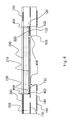
- the PCB 100 Since the PCBA works as a fingerprint reader module, the PCB 100 has several key parts. Please see FIG. 4 . They are a first electrically conductive layer 110 , a first insulation layer 120 , a second electrically conductive layer 130 , a second insulation layer 140 and a third electrically conductive layer 150 listed in sequence from top to bottom in FIG. 4 .
- the first electrically conductive layer 110 forms a specific circuit on partial of a top surface of the first insulation layer 120 .
- the first electrically conductive layer 110 shown in FIG. 4 is in form of discontinuous conductors.
- the conductors are made of copper or other metals or alloys.
- the conductors are not connected to each in the cross section, they are linked to form the circuit when the first electrically conductive layer 110 is taken out from the PCB 100 .
- Layout is a common technique, it is not described here. It should be noticed that the second electrically conductive layer 130 and the third electrically conductive layer 150 are illustrated in the same way.
- the first insulation layer 120 is used to separate the first electrically conductive layer 110 and the second electrically conductive layer 130 . Meanwhile, the first insulation layer 120 also provides enough hardness to the PCB 100 , preventing from breaking off.
- the first insulation layer 120 has a first opening 122 (please refer to FIG. 5 ) formed therein.
- the second electrically conductive layer 130 forms another specific circuit and a number of connectors 132 between the first insulation layer 120 and the second insulation layer 140 .
- the connectors 132 are used to electrically connect to the bonding pads in the image sensing chip 200 . If we take out the first electrically conductive layer 110 from the PCB 100 , a top view will look like FIG. 5 .
- the connectors 132 are extended and formed on a platform 143 .
- the platform 143 is formed on a top surface of the second insulation layer 140 enclosed by peripherals of the first opening 122 .
- the second insulation layer 140 basically has the same functions as the first insulation layer 120 . It has a second opening 142 formed therein. However, as shown in FIG. 5 , the second opening 142 is smaller than the first opening 122 and formed beneath the first opening 122 .
- the third electrically conductive layer 150 forms still another specific circuit on partial of a bottom surface of the second insulation layer 140 .
- the image sensing chip 200 has a number of bonding pads 220 .
- the image sensing chip 200 also has a sensor portion 210 facing down through the second opening 142 . It is fixed on the platform 143 with each bonding pad 220 connected to one corresponding connector 132 .
- the PCBA further includes a protection layer 300 .
- the protection layer 300 forms over some portions of the top surface of the first insulation layer 120 , the first electrically conductive layer 110 and a surface of the image sensing chip 200 opposite to the sensor portion 210 .
- the fingerprint reader module (the PCBA functions) is upside down when it is used. Please see FIG. 6 .
- a finger is scanned for its fingerprint in the second opening 142 .
- the protection layer 300 can provide resistance when a force is exerted on the sensor portion 210 .
- the protection layer is formed by a non-conductive adhesive.
- the non-conductive adhesive is epoxy resin. It can be also made by organic coating material.
- non-conductive adhesive can be further applied along peripherals of the sensor portion 210 and adjacent portions of the second electrically conductive layer 130 and/or the second insulation layer 140 as a fixture 406 .
- the fixture 406 can provide tension when the finger exerts force on the sensor portion 210 .
- the bonding pad 220 and the corresponding connector 132 are connected by a conductive adhesive 402 .
- a conductive adhesive 402 Preferable, silver paste is used as the conductive adhesive 402 for its conductivity and adhesive.
- the conductive adhesive is printed on the top of each bonding pad 220 , respectively, before they are connected to the corresponding connector 132 .
- gaps between sidewalls of the first insulation layer 120 and peripherals of the image sensing chip 200 are filled by a non-conductive adhesive 404 .
- Epoxy resin is a good choice for the non-conductive adhesive 404 .
- the non-conductive adhesive 404 can assist to fix the image sensing chip 200 into first opening 122 while no more current leakage may occur.
- the size of the sensor portion 210 should be substantially the same as or slightly smaller than that of the second opening 142 .
- width of the fixture 406 depends on the gaps between the sensor portion 210 and the second opening 142 as shown in FIG. 4 .
- the fixture 406 may cover portions of the peripheral of the sensor portion 210 .
- the shape of the first opening 122 is similar to that of the image sensing chip but large enough in size so that the image sensing chip 200 can be allocated in the first opening 122 . This is to reduce the risk that the image sensing chip 200 may slide in the second opening 142 when the finger exerts its force.
- a step gap between a level of the surface opposite to the sensor portion 210 and the first insulation layer 120 and/or the first electrically conductive layer 110 after the image sensing chip 200 is fixed on the platform is less than 0.1 mm.
- the protection layer 300 can be attached well without any being torn off due to a large step gap.
- the PCBA has a procedure to assemble the PCBA. Please refer to FIG. 7 to FIG. 11 at the same time.
- FIG. 7 is a flow chart of the procedure for assembling the PCBA according to the present invention.
- FIG. 8 to FIG. 11 are used to illustrate each step in the procedure.
Landscapes
- Engineering & Computer Science (AREA)
- Microelectronics & Electronic Packaging (AREA)
- Physics & Mathematics (AREA)
- General Physics & Mathematics (AREA)
- Condensed Matter Physics & Semiconductors (AREA)
- Computer Hardware Design (AREA)
- Power Engineering (AREA)
- Manufacturing & Machinery (AREA)
- Human Computer Interaction (AREA)
- Multimedia (AREA)
- Theoretical Computer Science (AREA)
- Image Input (AREA)
- Measurement Of Length, Angles, Or The Like Using Electric Or Magnetic Means (AREA)
- Solid State Image Pick-Up Elements (AREA)
- Geometry (AREA)
- Measurement Of The Respiration, Hearing Ability, Form, And Blood Characteristics Of Living Organisms (AREA)
Abstract
A printed circuit board assembly (PCBA) and a method to assemble the PCBA are disclosed. The PCBA includes a printed circuit board (PCB), an image sensing chip and a protection layer. The PCB includes a first insulation layer, a second insulation layer, a first electrically conductive layer, a second electrically conductive layer, and a third electrically conductive layer. The image sensing chip has a number of bonding pads with a sensor portion facing down through the second opening. The PCBA can function as an image sensing module and make the module have the thinnest thickness.
Description
The present invention relates to a printed circuit board assembly. More particularly, the present invention relates to a printed circuit board assembly with an image sensor mounted thereon.
A silicon chip, or integrated circuit (IC), is the core element of an electronic device and usually comes in packaged form. With the development of manufacturing technology and requirement of compact design for end products, various packaging methods were invented to meet the demand. At most of the time, silicon chips are sealed within a protection material such as epoxy resin. There are certain cases, particularly when the silicon chip is a sensor device such as a fingerprint sensor chip, that the silicon chip needs to be mount on a substrate and has the surface exposed. Meanwhile, for a fingerprint reader device, the thickness of the packaged sensor must be as low as possible. Hence, the technique of bonding the silicon chip to the substrate plays a very important role. The bonding needs to ensure good circuit connectivity formed therebetween, and to be rigid enough to sustain the fingerprint reader sensor with shear force exerted by a finger.
Conventional wire bonding is applicable to the above requirement. Please refer to FIG. 1 . A PCB 1 has an opening 2. A chip 3 in form of a die would like to be mounted on the PCB 1, over the opening 2. There are many attachment pads 4 on one surface of the chip 3. Some connectors 5 are arranged on the PCB 1. By wire bonding, gold wires 6 are formed to link the related attachment pads 4 and the connectors 5. In order to fix the PCB 1 and the chip 3, a layer of glue (not shown) may be applied on the interface between the PCB 1 and the chip 3. For some electronic devices, thickness is much concerned. Wire bonding for the PCB 1 and the chip 3 is not proper for them. This is because the height H of the gold wires 6 over the PCB 1 will occupy more space above the PCB 1 and make the thickness of the electronic device thicker.
Flip chip technology is another commonly used means to implement the above requirement. Take the same elements used in FIG. 1 for illustration. Please see FIG. 2 . It should be noticed that near the end of the manufacturing process, the attachment pads 4 of the chip 3 are metalized to make them more receptive to solders. This typically consists of several treatments. Small dots of solder balls 7 are then deposited on each metalized pad 4. The chips 3 are then cut out of the wafer as normal. To attach the flipped chips 3 into the PCB 1, the chip 3 is inverted to bring the solder balls 7 down onto the connectors 5 on the underlying PCB 1. The solder balls 7 are then re-melted to produce an electrical connection, typically using a thermosonic bonding or alternatively a reflow solder process. This also leaves a small space between the chip's circuitry and the underlying mounting.
One challenge of the flip chip technology is heat dissipation for thermal stress in the chip 3. An adhesive (not shown) may be used as a heat bridge to ensure the solder balls 7 are not stressed due to differential heating of the chip 3 and the PCB 1. The adhesive distributes the thermal expansion mismatch between the chip 3 and the PCB 1, preventing stress concentration in the solder balls 7 which would lead to premature failure. When fan-outs of logic gates of a chip increases and associated pads for soldering become more and tiny, efficiency of heating dissipation of such adhesive for the solder balls get worse. Meanwhile, if the chip 3 is a fingerprint reader sensor chip, the binding ability between the chip and the PCB may not sufficient to resist the force exerted by a finger.
Therefore, an improved PCBA structure with a chip, especially an image sensor chip, mounted on a PCB over an opening is still desired. More particularly, the binding ability between the chip and the PCB should resist external force exerted onto the chip.
This paragraph extracts and compiles some features of the present invention; other features will be disclosed in the follow-up paragraphs. It is intended to cover various modifications and similar arrangements included within the spirit and scope of the appended claims.
In accordance with an aspect of the present invention, a printed circuit board assembly (PCBA) is disclosed. The PCBA includes: a printed circuit board (PCB), comprising: a first insulation layer having a first opening formed therein; a second insulation layer having a second opening formed therein; a first electrically conductive layer, formed a specific circuit on partial of a top surface of the first insulation layer; a second electrically conductive layer, formed another specific circuit and a plurality of connectors between the first insulation layer and the second insulation layer; and a third electrically conductive layer, formed still another specific circuit on partial of a bottom surface of the second insulation layer, and an image sensing chip, having a plurality of bonding pads with a sensor portion facing down through the second opening, and fixed on the platform with each bonding pad connected to one corresponding connector.
The second opening is smaller than the first opening and formed beneath the first opening. A platform is formed on a top surface of the second insulation layer enclosed by peripherals of the first opening. The plurality of connectors are formed on the platform.
According to the present invention, the bonding pad and the corresponding connector are connected by a conductive adhesive. The conductive adhesive is silver paste. Gaps between sidewalls of the first insulation layer and peripherals of the image sensing chip are filled by a non-conductive adhesive. The non-conductive adhesive is epoxy resin.
The PCBA further has a protection layer formed over some portions of the top surface of the first insulation layer, the first electrically conductive layer and a surface of the image sensing chip opposite to the sensor portion for providing resistance when a force is exerted on the sensor portion. The protection layer is formed by a non-conductive adhesive. The non-conductive adhesive is epoxy resin. The non-conductive adhesive is further applied along peripherals of the sensor portion and adjacent portions of the second electrically conductive layer and/or the second insulation layer. The conductive adhesive is printed on the top of each bonding pad, respectively, before connecting to the corresponding connector. The image sensing chip may be a fingerprint reader sensor chip.
The size of the sensor portion is substantially the same as or slightly smaller than that of the second opening, and the shape of the first opening is the similar to that of the image sensing chip but large enough in size so that the image sensing chip can be allocated in the first opening.
Preferably, a step gap between a level of the surface opposite to the sensor portion and the first insulation layer and/or the first electrically conductive layer after the image sensing chip is fixed on the platform is less than 0.1 mm.
In accordance with another aspect of the present invention, a method for assembling the PCBA mention above includes the steps of: applying the conductive adhesive on the bounding pads; placing the image sensing chip through the first opening with the sensor portion facing down, connectors electrically connected to and linked by the conductive adhesive, and sensor portion exposed by the second opening; filling the gaps with a non-conductive adhesive; and forming a protection layer over the top surface of the first insulation layer and a surface opposite to the sensor portion for providing resistance when a force is exerted on the sensor portion.
The present invention will now be described more specifically with reference to the following embodiment.
Please refer to FIG. 3 to FIG. 11 . An embodiment is illustrated. FIG. 3 is a top view of a printed circuit board assembly (PCBA). The PCBA includes a printed circuit board (PCB) 100 and an image sensing chip 200. There are many image sensing chips can be used. In this embodiment, the image sensing chip 200 is a fingerprint reader. Please notice the sketches in the drawings may not be made according to the proportion. They are used for illustration only. The image sensing chip 200 may occupy less space than the PCB 100 in the PCBA. It should be noticed that in FIG. 3 , a cross-sectional line AA′ is marked. For a better understanding, the cross section cut by line AA′ is used in following drawings.
Since the PCBA works as a fingerprint reader module, the PCB 100 has several key parts. Please see FIG. 4 . They are a first electrically conductive layer 110, a first insulation layer 120, a second electrically conductive layer 130, a second insulation layer 140 and a third electrically conductive layer 150 listed in sequence from top to bottom in FIG. 4 . The first electrically conductive layer 110 forms a specific circuit on partial of a top surface of the first insulation layer 120. As one can see, the first electrically conductive layer 110 shown in FIG. 4 is in form of discontinuous conductors. The conductors are made of copper or other metals or alloys. Although the conductors are not connected to each in the cross section, they are linked to form the circuit when the first electrically conductive layer 110 is taken out from the PCB 100. Layout is a common technique, it is not described here. It should be noticed that the second electrically conductive layer 130 and the third electrically conductive layer 150 are illustrated in the same way.
The first insulation layer 120 is used to separate the first electrically conductive layer 110 and the second electrically conductive layer 130. Meanwhile, the first insulation layer 120 also provides enough hardness to the PCB 100, preventing from breaking off. The first insulation layer 120 has a first opening 122 (please refer to FIG. 5 ) formed therein. The second electrically conductive layer 130 forms another specific circuit and a number of connectors 132 between the first insulation layer 120 and the second insulation layer 140. The connectors 132 are used to electrically connect to the bonding pads in the image sensing chip 200. If we take out the first electrically conductive layer 110 from the PCB 100, a top view will look like FIG. 5 . The connectors 132 are extended and formed on a platform 143. The platform 143 is formed on a top surface of the second insulation layer 140 enclosed by peripherals of the first opening 122.
The second insulation layer 140 basically has the same functions as the first insulation layer 120. It has a second opening 142 formed therein. However, as shown in FIG. 5 , the second opening 142 is smaller than the first opening 122 and formed beneath the first opening 122. The third electrically conductive layer 150 forms still another specific circuit on partial of a bottom surface of the second insulation layer 140.
The image sensing chip 200 has a number of bonding pads 220. The image sensing chip 200 also has a sensor portion 210 facing down through the second opening 142. It is fixed on the platform 143 with each bonding pad 220 connected to one corresponding connector 132.
The PCBA further includes a protection layer 300. Please see FIG. 5 again. The protection layer 300 forms over some portions of the top surface of the first insulation layer 120, the first electrically conductive layer 110 and a surface of the image sensing chip 200 opposite to the sensor portion 210. It should be emphasized that the fingerprint reader module (the PCBA functions) is upside down when it is used. Please see FIG. 6 . A finger is scanned for its fingerprint in the second opening 142. The protection layer 300 can provide resistance when a force is exerted on the sensor portion 210. The protection layer is formed by a non-conductive adhesive. Preferably, the non-conductive adhesive is epoxy resin. It can be also made by organic coating material. In addition, the non-conductive adhesive can be further applied along peripherals of the sensor portion 210 and adjacent portions of the second electrically conductive layer 130 and/or the second insulation layer 140 as a fixture 406. The fixture 406 can provide tension when the finger exerts force on the sensor portion 210.
For linkage of some components mentioned, there many suitable ways. For example, the bonding pad 220 and the corresponding connector 132 are connected by a conductive adhesive 402. Preferable, silver paste is used as the conductive adhesive 402 for its conductivity and adhesive. The conductive adhesive is printed on the top of each bonding pad 220, respectively, before they are connected to the corresponding connector 132. Besides, gaps between sidewalls of the first insulation layer 120 and peripherals of the image sensing chip 200 are filled by a non-conductive adhesive 404. Epoxy resin is a good choice for the non-conductive adhesive 404. The non-conductive adhesive 404 can assist to fix the image sensing chip 200 into first opening 122 while no more current leakage may occur.
According to the present invention, the size of the sensor portion 210 should be substantially the same as or slightly smaller than that of the second opening 142. Thus, width of the fixture 406 depends on the gaps between the sensor portion 210 and the second opening 142 as shown in FIG. 4 . Or the fixture 406 may cover portions of the peripheral of the sensor portion 210. Meanwhile, the shape of the first opening 122 is similar to that of the image sensing chip but large enough in size so that the image sensing chip 200 can be allocated in the first opening 122. This is to reduce the risk that the image sensing chip 200 may slide in the second opening 142 when the finger exerts its force. A step gap between a level of the surface opposite to the sensor portion 210 and the first insulation layer 120 and/or the first electrically conductive layer 110 after the image sensing chip 200 is fixed on the platform is less than 0.1 mm. Thus, the protection layer 300 can be attached well without any being torn off due to a large step gap.
The PCBA has a procedure to assemble the PCBA. Please refer to FIG. 7 to FIG. 11 at the same time. FIG. 7 is a flow chart of the procedure for assembling the PCBA according to the present invention. FIG. 8 to FIG. 11 are used to illustrate each step in the procedure.
First, apply the conductive adhesive 402 on the bounding pads 220 (S01, FIG. 8 ). Then, place the image sensing chip 200 through the first opening 122 with the sensor portion 210 facing down, connectors 132 electrically connected to and linked by the conductive adhesive 402, and sensor portion 210 exposed by the second opening 142 (S02, FIG. 9 ). Next, fill the gaps with a non-conductive adhesive 404 (S03, FIG. 10 ). Finally, form the protection layer 300 over the top surface of the first insulation layer 120 and a surface opposite to the sensor portion 210 for providing resistance when a force is exerted on the sensor portion 210 (S04, FIG. 11 ).
While the invention has been described in terms of what is presently considered to be the most practical and preferred embodiment, it is to be understood that the invention needs not be limited to the disclosed embodiment. On the contrary, it is intended to cover various modifications and similar arrangements included within the spirit and scope of the appended claims, which are to be accorded with the broadest interpretation so as to encompass all such modifications and similar structures.
Claims (12)
1. A printed circuit board assembly (PCBA), comprising:
a printed circuit board (PCB), comprising:
a first insulation layer, having a first opening formed therein;
a second insulation layer, having a second opening formed therein;
a first electrically conductive layer, forming a first specific circuit on a partial top surface of the first insulation layer;
a second electrically conductive layer, forming a second specific circuit and a plurality of connectors between the first insulation layer and the second insulation layer; and
a third electrically conductive layer, forming a third specific circuit on a partial bottom surface of the second insulation layer,
wherein the second opening is smaller than the first opening and formed beneath the first opening; a platform is formed on a top surface of the second insulation layer enclosed by peripherals of the first opening; the plurality of connectors are formed on the platform;
an image sensing chip, having a plurality of bonding pads with a sensor portion facing down through the second opening, and fixed on the platform with each bonding pad connected to one corresponding connector; and
a protection layer formed over some portions of the top surface of the first insulation layer, the first electrically conductive layer and a whole bottom surface of the image sensing chip opposite to the sensor portion for providing resistance when a force is exerted on the sensor portion,
wherein the first insulation layer and the whole bottom surface of the image sensing chip together form a flat surface for the protection layer to be formed thereon; and
wherein a non-conductive adhesive is applied in gaps between the sensor portion and the second opening while the sensor portion has a size smaller than the second opening or applied along peripheral of the sensor portion while the sensor portion has a size the same as the second opening to form a fixture to provide tension when a finger exerts force on the sensor portion of the image sensing chip.
2. The PCBA according to claim 1 , wherein the bonding pad and the corresponding connector are connected by a conductive adhesive.
3. The PCBA according to claim 2 , wherein the conductive adhesive is silver paste.
4. The PCBA according to claim 1 , wherein the non-conductive adhesive is further included in gaps between sidewalls of the first insulation layer and peripherals of the image sensing chip.
5. The PCBA according to claim 4 , wherein the non-conductive adhesive is epoxy resin.
6. The PCBA according to claim 1 , wherein the protection layer is formed by the non-conductive adhesive.
7. The PCBA according to claim 6 , the non-conductive adhesive is further applied along peripherals of the sensor portion and adjacent portions of the second electrically conductive layer and/or the second insulation layer.
8. The PCBA according to claim 1 , wherein the protection layer is made of organic coating material.
9. The PCBA according to claim 2 , wherein the conductive adhesive is printed on the top of each bonding pad, respectively, before connecting to the corresponding connector.
10. The PCBA according to claim 1 , wherein the image sensing chip is a fingerprint reader sensor chip.
11. The PCBA according to claim 1 , wherein the size of the sensor portion is substantially the same as or slightly smaller than that of the second opening, and the shape of the first opening is the similar to that of the image sensing chip but large enough in size so that the image sensing chip can be allocated in the first opening.
12. The PCBA according to claim 1 , wherein a step gap between a level of a surface opposite to the sensor portion and the first insulation layer and/or the first electrically conductive layer after the image sensing chip is fixed on the platform is less than 0.1 mm.
Priority Applications (1)
| Application Number | Priority Date | Filing Date | Title |
|---|---|---|---|
| US14/543,936 US10121043B2 (en) | 2014-11-18 | 2014-11-18 | Printed circuit board assembly with image sensor mounted thereon |
Applications Claiming Priority (1)
| Application Number | Priority Date | Filing Date | Title |
|---|---|---|---|
| US14/543,936 US10121043B2 (en) | 2014-11-18 | 2014-11-18 | Printed circuit board assembly with image sensor mounted thereon |
Publications (2)
| Publication Number | Publication Date |
|---|---|
| US20160141235A1 US20160141235A1 (en) | 2016-05-19 |
| US10121043B2 true US10121043B2 (en) | 2018-11-06 |
Family
ID=55962360
Family Applications (1)
| Application Number | Title | Priority Date | Filing Date |
|---|---|---|---|
| US14/543,936 Active 2036-12-26 US10121043B2 (en) | 2014-11-18 | 2014-11-18 | Printed circuit board assembly with image sensor mounted thereon |
Country Status (1)
| Country | Link |
|---|---|
| US (1) | US10121043B2 (en) |
Cited By (2)
| Publication number | Priority date | Publication date | Assignee | Title |
|---|---|---|---|---|
| US20210391226A1 (en) * | 2020-06-15 | 2021-12-16 | Stmicroelectronics, Inc. | Semiconductor device packages having cap with integrated electrical leads |
| US20220270960A1 (en) * | 2021-02-23 | 2022-08-25 | Texas Instruments Incorporated | Open-Cavity Package for Chip Sensor |
Families Citing this family (8)
| Publication number | Priority date | Publication date | Assignee | Title |
|---|---|---|---|---|
| TWM544047U (en) * | 2015-02-11 | 2017-06-21 | Tron Intelligence Inc | Improved packaging structure of fingerprint recognition image optics |
| KR102340053B1 (en) * | 2015-06-18 | 2021-12-16 | 삼성전기주식회사 | Printed circuit board and method of manufacturing the same |
| KR101904969B1 (en) | 2016-07-29 | 2018-10-10 | 삼성디스플레이 주식회사 | Display device |
| CN106653616A (en) | 2016-11-22 | 2017-05-10 | 苏州晶方半导体科技股份有限公司 | Encapsulation method and encapsulation structure of fingerprint sensor chip |
| US10804188B2 (en) * | 2018-09-07 | 2020-10-13 | Intel Corporation | Electronic device including a lateral trace |
| KR102185047B1 (en) * | 2019-05-20 | 2020-12-01 | 삼성전기주식회사 | Camera Module |
| KR102163694B1 (en) * | 2019-06-21 | 2020-10-08 | 시그네틱스 주식회사 | Fingerprint recognition sensor package |
| CN113594216B (en) * | 2021-07-29 | 2022-05-31 | 惠科股份有限公司 | OLED display panel and display device |
Citations (4)
| Publication number | Priority date | Publication date | Assignee | Title |
|---|---|---|---|---|
| US6661084B1 (en) * | 2000-05-16 | 2003-12-09 | Sandia Corporation | Single level microelectronic device package with an integral window |
| US6825551B1 (en) * | 1999-09-02 | 2004-11-30 | Stmicroelectronics S.A. | Method for packaging a semiconductor chip containing sensors and resulting package |
| US7851246B2 (en) * | 2007-12-27 | 2010-12-14 | Stats Chippac, Ltd. | Semiconductor device with optical sensor and method of forming interconnect structure on front and backside of the device |
| US20130221452A1 (en) * | 2011-09-15 | 2013-08-29 | Stats Chippac, Ltd. | Semiconductor Device and Method of Forming Semiconductor Die with Active Region Responsive to External Stimulus |
-
2014
- 2014-11-18 US US14/543,936 patent/US10121043B2/en active Active
Patent Citations (4)
| Publication number | Priority date | Publication date | Assignee | Title |
|---|---|---|---|---|
| US6825551B1 (en) * | 1999-09-02 | 2004-11-30 | Stmicroelectronics S.A. | Method for packaging a semiconductor chip containing sensors and resulting package |
| US6661084B1 (en) * | 2000-05-16 | 2003-12-09 | Sandia Corporation | Single level microelectronic device package with an integral window |
| US7851246B2 (en) * | 2007-12-27 | 2010-12-14 | Stats Chippac, Ltd. | Semiconductor device with optical sensor and method of forming interconnect structure on front and backside of the device |
| US20130221452A1 (en) * | 2011-09-15 | 2013-08-29 | Stats Chippac, Ltd. | Semiconductor Device and Method of Forming Semiconductor Die with Active Region Responsive to External Stimulus |
Cited By (2)
| Publication number | Priority date | Publication date | Assignee | Title |
|---|---|---|---|---|
| US20210391226A1 (en) * | 2020-06-15 | 2021-12-16 | Stmicroelectronics, Inc. | Semiconductor device packages having cap with integrated electrical leads |
| US20220270960A1 (en) * | 2021-02-23 | 2022-08-25 | Texas Instruments Incorporated | Open-Cavity Package for Chip Sensor |
Also Published As
| Publication number | Publication date |
|---|---|
| US20160141235A1 (en) | 2016-05-19 |
Similar Documents
| Publication | Publication Date | Title |
|---|---|---|
| US10121043B2 (en) | Printed circuit board assembly with image sensor mounted thereon | |
| US9281339B1 (en) | Method for mounting chip on printed circuit board | |
| TW473950B (en) | Semiconductor device and its manufacturing method, manufacturing apparatus, circuit base board and electronic machine | |
| US9760754B2 (en) | Printed circuit board assembly forming enhanced fingerprint module | |
| US8283767B1 (en) | Dual laminate package structure with embedded elements | |
| US8451621B2 (en) | Semiconductor component and method of manufacture | |
| US7956453B1 (en) | Semiconductor package with patterning layer and method of making same | |
| CN101221946A (en) | Semiconductor package and method for manufacturing system-in-package module | |
| JPH09330996A (en) | Electronic package | |
| CN1979836A (en) | Semiconductor device and electronic control unit using the same | |
| CN101258609A (en) | Vertical electronics packaging structure using wires arranged on laminated boards | |
| TW200504952A (en) | Method of manufacturing semiconductor package and method of manufacturing semiconductor device | |
| JP2009141169A (en) | Semiconductor device | |
| JP4828164B2 (en) | Interposer and semiconductor device | |
| CN212136426U (en) | Flip chip and chip packaging structure | |
| US20070063347A1 (en) | Packages, anisotropic conductive films, and conductive particles utilized therein | |
| JP3695458B2 (en) | Semiconductor device, circuit board and electronic equipment | |
| JP2008218758A (en) | Electronic circuit mounting structure | |
| TWI613771B (en) | Semiconductor package | |
| CN113851437B (en) | Flip chip and chip packaging structure | |
| CN106611752B (en) | Electrical connection structure between front surface and back surface of chip and manufacturing method thereof | |
| CN101599474B (en) | Integrated circuit module and manufacturing method thereof | |
| CN105742253B (en) | Printed circuit board assembly for mounting image sensor | |
| KR102068162B1 (en) | Terminal structure of chip package | |
| JP2008270511A (en) | Electronic device |
Legal Events
| Date | Code | Title | Description |
|---|---|---|---|
| AS | Assignment |
Owner name: SUNASIC TECHNOLOGIES, INC., TAIWAN Free format text: ASSIGNMENT OF ASSIGNORS INTEREST;ASSIGNORS:LIN, CHI-CHOU;HE, ZHENG-PING;REEL/FRAME:034194/0602 Effective date: 20141107 |
|
| STCF | Information on status: patent grant |
Free format text: PATENTED CASE |
|
| MAFP | Maintenance fee payment |
Free format text: PAYMENT OF MAINTENANCE FEE, 4TH YR, SMALL ENTITY (ORIGINAL EVENT CODE: M2551); ENTITY STATUS OF PATENT OWNER: SMALL ENTITY Year of fee payment: 4 |