US10114562B2 - Adaptive block allocation in nonvolatile memory - Google Patents
Adaptive block allocation in nonvolatile memory Download PDFInfo
- Publication number
- US10114562B2 US10114562B2 US14/488,037 US201414488037A US10114562B2 US 10114562 B2 US10114562 B2 US 10114562B2 US 201414488037 A US201414488037 A US 201414488037A US 10114562 B2 US10114562 B2 US 10114562B2
- Authority
- US
- United States
- Prior art keywords
- plane
- blocks
- data
- good
- block
- Prior art date
- Legal status (The legal status is an assumption and is not a legal conclusion. Google has not performed a legal analysis and makes no representation as to the accuracy of the status listed.)
- Active, expires
Links
Images


Classifications
-
- G—PHYSICS
- G06—COMPUTING OR CALCULATING; COUNTING
- G06F—ELECTRIC DIGITAL DATA PROCESSING
- G06F3/00—Input arrangements for transferring data to be processed into a form capable of being handled by the computer; Output arrangements for transferring data from processing unit to output unit, e.g. interface arrangements
- G06F3/06—Digital input from, or digital output to, record carriers, e.g. RAID, emulated record carriers or networked record carriers
- G06F3/0601—Interfaces specially adapted for storage systems
- G06F3/0602—Interfaces specially adapted for storage systems specifically adapted to achieve a particular effect
- G06F3/0614—Improving the reliability of storage systems
- G06F3/0617—Improving the reliability of storage systems in relation to availability
-
- G—PHYSICS
- G06—COMPUTING OR CALCULATING; COUNTING
- G06F—ELECTRIC DIGITAL DATA PROCESSING
- G06F12/00—Accessing, addressing or allocating within memory systems or architectures
- G06F12/02—Addressing or allocation; Relocation
- G06F12/0223—User address space allocation, e.g. contiguous or non contiguous base addressing
- G06F12/023—Free address space management
- G06F12/0238—Memory management in non-volatile memory, e.g. resistive RAM or ferroelectric memory
- G06F12/0246—Memory management in non-volatile memory, e.g. resistive RAM or ferroelectric memory in block erasable memory, e.g. flash memory
-
- G—PHYSICS
- G06—COMPUTING OR CALCULATING; COUNTING
- G06F—ELECTRIC DIGITAL DATA PROCESSING
- G06F3/00—Input arrangements for transferring data to be processed into a form capable of being handled by the computer; Output arrangements for transferring data from processing unit to output unit, e.g. interface arrangements
- G06F3/06—Digital input from, or digital output to, record carriers, e.g. RAID, emulated record carriers or networked record carriers
- G06F3/0601—Interfaces specially adapted for storage systems
- G06F3/0628—Interfaces specially adapted for storage systems making use of a particular technique
- G06F3/0638—Organizing or formatting or addressing of data
- G06F3/064—Management of blocks
-
- G—PHYSICS
- G06—COMPUTING OR CALCULATING; COUNTING
- G06F—ELECTRIC DIGITAL DATA PROCESSING
- G06F3/00—Input arrangements for transferring data to be processed into a form capable of being handled by the computer; Output arrangements for transferring data from processing unit to output unit, e.g. interface arrangements
- G06F3/06—Digital input from, or digital output to, record carriers, e.g. RAID, emulated record carriers or networked record carriers
- G06F3/0601—Interfaces specially adapted for storage systems
- G06F3/0668—Interfaces specially adapted for storage systems adopting a particular infrastructure
- G06F3/0671—In-line storage system
- G06F3/0683—Plurality of storage devices
- G06F3/0688—Non-volatile semiconductor memory arrays
-
- G—PHYSICS
- G06—COMPUTING OR CALCULATING; COUNTING
- G06F—ELECTRIC DIGITAL DATA PROCESSING
- G06F12/00—Accessing, addressing or allocating within memory systems or architectures
- G06F12/02—Addressing or allocation; Relocation
- G06F12/08—Addressing or allocation; Relocation in hierarchically structured memory systems, e.g. virtual memory systems
- G06F12/0802—Addressing of a memory level in which the access to the desired data or data block requires associative addressing means, e.g. caches
- G06F12/0804—Addressing of a memory level in which the access to the desired data or data block requires associative addressing means, e.g. caches with main memory updating
-
- G—PHYSICS
- G06—COMPUTING OR CALCULATING; COUNTING
- G06F—ELECTRIC DIGITAL DATA PROCESSING
- G06F12/00—Accessing, addressing or allocating within memory systems or architectures
- G06F12/02—Addressing or allocation; Relocation
- G06F12/08—Addressing or allocation; Relocation in hierarchically structured memory systems, e.g. virtual memory systems
- G06F12/0802—Addressing of a memory level in which the access to the desired data or data block requires associative addressing means, e.g. caches
- G06F12/0866—Addressing of a memory level in which the access to the desired data or data block requires associative addressing means, e.g. caches for peripheral storage systems, e.g. disk cache
-
- G—PHYSICS
- G06—COMPUTING OR CALCULATING; COUNTING
- G06F—ELECTRIC DIGITAL DATA PROCESSING
- G06F2212/00—Indexing scheme relating to accessing, addressing or allocation within memory systems or architectures
- G06F2212/72—Details relating to flash memory management
- G06F2212/7201—Logical to physical mapping or translation of blocks or pages
-
- G—PHYSICS
- G06—COMPUTING OR CALCULATING; COUNTING
- G06F—ELECTRIC DIGITAL DATA PROCESSING
- G06F2212/00—Indexing scheme relating to accessing, addressing or allocation within memory systems or architectures
- G06F2212/72—Details relating to flash memory management
- G06F2212/7204—Capacity control, e.g. partitioning, end-of-life degradation
-
- G—PHYSICS
- G06—COMPUTING OR CALCULATING; COUNTING
- G06F—ELECTRIC DIGITAL DATA PROCESSING
- G06F2212/00—Indexing scheme relating to accessing, addressing or allocation within memory systems or architectures
- G06F2212/72—Details relating to flash memory management
- G06F2212/7208—Multiple device management, e.g. distributing data over multiple flash devices
-
- G—PHYSICS
- G06—COMPUTING OR CALCULATING; COUNTING
- G06F—ELECTRIC DIGITAL DATA PROCESSING
- G06F2212/00—Indexing scheme relating to accessing, addressing or allocation within memory systems or architectures
- G06F2212/72—Details relating to flash memory management
- G06F2212/7211—Wear leveling
Definitions
- This application relates to the operation of re-programmable nonvolatile memory systems such as semiconductor flash memory systems, and, more specifically, to operation of multiple planes in such systems.
- Solid-state memory capable of nonvolatile storage of charge, particularly in the form of EEPROM and flash EEPROM packaged as a small form factor card, has recently become the storage of choice in a variety of mobile and handheld devices, notably information appliances and consumer electronics products.
- RAM random access memory
- flash memory is non-volatile, and retains its stored data even after power is turned off.
- ROM read only memory
- flash memory is rewritable similar to a disk storage device. Flash memory, both embedded and in the form of a removable card is ideally suited in the mobile and handheld environment because of its small size, low power consumption, high speed and high reliability features.
- Flash EEPROM is similar to EEPROM (electrically erasable and programmable read-only memory) in that it is a non-volatile memory that can be erased and have new data written or “programmed” into their memory cells. Both utilize a floating (unconnected) conductive gate, in a field effect transistor structure, positioned over a channel region in a semiconductor substrate, between source and drain regions. A control gate is then provided over the floating gate. The threshold voltage characteristic of the transistor is controlled by the amount of charge that is retained on the floating gate. That is, for a given level of charge on the floating gate, there is a corresponding voltage (threshold) that is applied to the control gate before the transistor is turned “on” to permit conduction between its source and drain regions.
- flash memory such as Flash EEPROM allows entire blocks of memory cells to be erased at the same time.
- Nonvolatile memory devices are also manufactured from memory cells with a dielectric layer for storing charge. Instead of the conductive floating gate elements described earlier, a dielectric layer is used. The charge for one data bit is localized in the dielectric layer adjacent to the drain, and the charge for the other data bit is localized in the dielectric layer adjacent to the source. Multi-state data storage is implemented by separately reading the binary states of the spatially separated charge storage regions within the dielectric.
- Memory cells of a typical flash EEPROM array are divided into discrete blocks of cells that are erased together. That is, the erase block is the erase unit, a minimum number of cells that are simultaneously erasable.
- Each erase block typically stores one or more pages of data, the page being the minimum unit of programming and reading, although more than one page may be programmed or read in parallel in different sub-arrays or planes.
- Each page typically stores one or more sectors of data, the size of the sector being defined by the host system.
- An example sector includes 512 bytes of user data, following a standard established with magnetic disk drives, plus some number of bytes of overhead information about the user data and/or the erase block in which they are stored.
- the array is typically divided into sub-arrays, commonly referred to as planes, which contain their own data registers and other circuits to allow parallel operation such that sectors of data may be programmed to or read from each of several or all the planes simultaneously.
- planes which contain their own data registers and other circuits to allow parallel operation such that sectors of data may be programmed to or read from each of several or all the planes simultaneously.
- An array on a single integrated circuit may be physically divided into planes, or each plane may be formed from a separate one or more integrated circuit chips.
- erase blocks may be linked together to form virtual blocks or metablocks. That is, each metablock is defined to include one erase block from each plane.
- unlinked blocks In a multi-plane non-volatile memory, good blocks of different planes are linked for parallel operation for storing long host writes with a high degree of parallelism. Where bad blocks in one or more planes result in unlinked blocks (odd blocks), the unlinked blocks are configured for individual operation to store short host writes and/or memory system management data.
- unlinked blocks may be configured as Single Level Cell (SLC) blocks while linked blocks may be configured as Multi Level Cell (MLC) blocks or SLC blocks.
- SLC Single Level Cell
- MLC Multi Level Cell
- An example of a method of operating a multi-plane flash memory array includes: identifying bad blocks in a first plane of the multi-plane flash memory array and designating a first number of good blocks of the first plane for storage of user data; identifying bad blocks in a second plane of the multi-plane flash memory array and designating a second number of good blocks of the second plane for storage of user data, the second number being greater than the first number; linking the first number of good blocks of the first plane with good blocks of the second plane to form the first number of metablocks, each of the first number of metablocks configured for parallel operation across the first and second planes; identifying a third number of good blocks in the second plane that are not linked, the third number being equal to the second number minus the first number; and configuring the third number of good blocks in the second plane for individual operation to store selected data.
- the selected data may include memory system management data that is stored by a memory controller.
- the memory system management data may include one or more of: boot code, file system data, logical-to-physical address mapping data, and bad block location data.
- the selected data may include short host writes of less than a threshold amount of data.
- the first number of metablocks may be configured for Multi Level Cell (MLC) operation and the third number of good blocks may be configured only for SLC operation.
- MLC Multi Level Cell
- a determination may be made that an individual block of the first number of blocks of the first plane has become bad; the individual block may be designated as a bad block and subsequent storage of user data in the individual block may be prohibited; the bad block may be unlinked from a corresponding good block of the second plane; and the corresponding good block of the second plane may be configured for individual operation to store selected data.
- the individual block may be designated as a bad block and subsequent storage of selected data in the individual block may be prohibited; the bad block may be unlinked from a corresponding good block of the first plane; the good block of the first plane may be linked with one of the third number of good blocks in the second plane; and the corresponding good block of the first plane and the good block of the second plane may be reconfigured for parallel operation as a metablock.
- the third number of good blocks in the second plane for individual operation, it may be determined that an individual block of the third number of blocks has become bad; and the individual block may be designated as a bad block and may be prohibited from subsequent storage of selected data.
- An example of a multi-plane nonvolatile memory system includes a first plane that includes a first number of good blocks; a second plane that includes a second number of good blocks that is greater than the first number; a first number of metablocks, an individual metablock formed from one good block of the first plane linked with one corresponding good block from the second plane; and a third number of individually operated blocks in the second plane that are not linked with any blocks of the first plane, the third number equal to the second number minus the first number.
- the first number of metablocks may store host writes of more than a threshold amount of data and the third number of individually operated blocks may be dedicated to storage of memory system management data and/or host writes of less than the threshold amount of data.
- the third number of individually operated blocks may be dedicated to storage of memory system management data including one or more of: boot code, file system data, logical-to-physical address mapping data, and bad block location data.
- At least an additional plane may contain an additional number of good blocks that is greater than the first number, the additional plane containing additional individually operated blocks.
- Configurable read/write circuits may have at least two modes of accessing stored including: (a) a parallel access mode that accesses the first and second planes in parallel, and (b) an individual access mode that accesses an individual block of either the first plane or the second plane at a time.
- Wear-leveling circuits may maintain write-erase cycle counts and apply wear leveling schemes including: (a) a first wear leveling scheme for metablocks and (b) a second wear leveling scheme for individually operated blocks.
- the first plane and the second plane may be monolithically formed in two or more physical levels of arrays of memory cells having an active area disposed above a silicon substrate. Circuitry associated with operation of the first plane and the second plane may be disposed above or within the silicon substrate.
- FIG. 1 illustrates schematically the main hardware components of a memory system.
- FIG. 2 illustrates a multi-plane memory array
- FIG. 3 illustrates formation of a metablock
- FIG. 4 illustrates a four-die memory array with one plane per die.
- FIG. 5 illustrates a two die memory with two planes in each die.
- FIG. 6 illustrates a two die memory with two planes with different numbers of bad blocks.
- FIG. 7 illustrates space utilization across four planes with different numbers of bad blocks in each plane.
- FIG. 8 illustrates an example of reconfiguration of odd blocks for individual operation.
- FIG. 9 illustrates an example of configuration of a multi-plane memory.
- FIG. 10 illustrates an example of configuration of linked and unlinked blocks.
- FIG. 11 illustrates an example of how data may be stored in a multi-plane memory.
- FIG. 12 illustrates an example of a new bad block in the plane with the largest number of bad blocks.
- FIG. 13 illustrates an example of a new bad block in a plane that is not the plane with the largest number of bad blocks.
- Semiconductor memory devices include volatile memory devices, such as dynamic random access memory (“DRAM”) or static random access memory (“SRAM”) devices, non-volatile memory devices, such as resistive random access memory (“ReRAM”), electrically erasable programmable read only memory (“EEPROM”), flash memory (which can also be considered a subset of EEPROM), ferroelectric random access memory (“FRAM”), and magnetoresistive random access memory (“MRAM”), and other semiconductor elements capable of storing information.
- volatile memory devices such as dynamic random access memory (“DRAM”) or static random access memory (“SRAM”) devices
- non-volatile memory devices such as resistive random access memory (“ReRAM”), electrically erasable programmable read only memory (“EEPROM”), flash memory (which can also be considered a subset of EEPROM), ferroelectric random access memory (“FRAM”), and magnetoresistive random access memory (“MRAM”), and other semiconductor elements capable of storing information.
- ReRAM resistive random access memory
- EEPROM electrically erasable
- the memory devices can be formed from passive and/or active elements, in any combinations.
- passive semiconductor memory elements include ReRAM device elements, which in some embodiments include a resistivity switching storage element, such as an anti-fuse, phase change material, etc., and optionally a steering element, such as a diode, etc.
- active semiconductor memory elements include EEPROM and flash memory device elements, which in some embodiments include elements containing a charge storage region, such as a floating gate, conductive nanoparticles, or a charge storage dielectric material.
- Multiple memory elements may be configured so that they are connected in series or so that each element is individually accessible.
- flash memory devices in a NAND configuration typically contain memory elements connected in series.
- a NAND memory array may be configured so that the array is composed of multiple strings of memory in which a string is composed of multiple memory elements sharing a single bit line and accessed as a group.
- memory elements may be configured so that each element is individually accessible, e.g., a NOR memory array.
- NAND and NOR memory configurations are exemplary, and memory elements may be otherwise configured.
- the semiconductor memory elements located within and/or over a substrate may be arranged in two or three dimensions, such as a two dimensional memory structure or a three dimensional memory structure.
- the semiconductor memory elements are arranged in a single plane or a single memory device level.
- memory elements are arranged in a plane (e.g., in an x-z direction plane) which extends substantially parallel to a major surface of a substrate that supports the memory elements.
- the substrate may be a wafer over or in which the layer of the memory elements are formed or it may be a carrier substrate which is attached to the memory elements after they are formed.
- the substrate may include a semiconductor such as silicon.
- the memory elements may be arranged in the single memory device level in an ordered array, such as in a plurality of rows and/or columns. However, the memory elements may be arrayed in non-regular or non-orthogonal configurations.
- the memory elements may each have two or more electrodes or contact lines, such as bit lines and word lines.
- a three dimensional memory array is arranged so that memory elements occupy multiple planes or multiple memory device levels, thereby forming a structure in three dimensions (i.e., in the x, y and z directions, where the y direction is substantially perpendicular and the x and z directions are substantially parallel to the major surface of the substrate).
- a three dimensional memory structure may be vertically arranged as a stack of multiple two dimensional memory device levels.
- a three dimensional memory array may be arranged as multiple vertical columns (e.g., columns extending substantially perpendicular to the major surface of the substrate, i.e., in the y direction) with each column having multiple memory elements in each column.
- the columns may be arranged in a two dimensional configuration, e.g., in an x-z plane, resulting in a three dimensional arrangement of memory elements with elements on multiple vertically stacked memory planes.
- Other configurations of memory elements in three dimensions can also constitute a three dimensional memory array.
- the memory elements may be coupled together to form a NAND string within a single horizontal (e.g., x-z) memory device levels.
- the memory elements may be coupled together to form a vertical NAND string that traverses across multiple horizontal memory device levels.
- Other three dimensional configurations can be envisioned wherein some NAND strings contain memory elements in a single memory level while other strings contain memory elements which span through multiple memory levels.
- Three dimensional memory arrays may also be designed in a NOR configuration and in a ReRAM configuration.
- a monolithic three dimensional memory array typically, one or more memory device levels are formed above a single substrate.
- the monolithic three dimensional memory array may also have one or more memory layers at least partially within the single substrate.
- the substrate may include a semiconductor such as silicon.
- the layers constituting each memory device level of the array are typically formed on the layers of the underlying memory device levels of the array.
- layers of adjacent memory device levels of a monolithic three dimensional memory array may be shared or have intervening layers between memory device levels.
- non-monolithic stacked memories can be constructed by forming memory levels on separate substrates and then stacking the memory levels atop each other. The substrates may be thinned or removed from the memory device levels before stacking, but as the memory device levels are initially formed over separate substrates, the resulting memory arrays are not monolithic three dimensional memory arrays. Further, multiple two dimensional memory arrays or three dimensional memory arrays (monolithic or non-monolithic) may be formed on separate chips and then packaged together to form a stacked-chip memory device.
- Associated circuitry is typically required for operation of the memory elements and for communication with the memory elements.
- memory devices may have circuitry used for controlling and driving memory elements to accomplish functions such as programming and reading.
- This associated circuitry may be on the same substrate as the memory elements and/or on a separate substrate.
- a controller for memory read-write operations may be located on a separate controller chip and/or on the same substrate as the memory elements.
- a flash memory includes a memory cell array and a controller.
- two integrated circuit devices (chips) 11 and 13 include an array 15 of memory cells (which may be 3D or planar) and various logic circuits 17 .
- the logic circuits 17 interface with a controller 19 on a separate chip through data, command and status circuits, and also provide addressing, data transfer and sensing, and other support to the array 13 .
- a number of memory array chips can be from one to many, depending upon the storage capacity provided.
- a memory cell array may be located on a single chip or may be comprised of memory cells on multiple chips. The controller and part or the entire array can alternatively be combined onto a single integrated circuit chip but this is currently not an economical alternative.
- An example of a controller 19 includes a microprocessor 21 , a read-only-memory (ROM) 23 primarily to store firmware and a buffer memory (RAM) 25 that may be used for the temporary storage of user data either being written to or read from the memory chips 11 and 13 .
- Circuits 27 interface with the memory array chip(s) and circuits 29 interface with a host though connections 31 . The integrity of data is in this example determined by calculating an ECC with circuits 33 dedicated to calculating the code. As user data is being transferred from the host to the flash memory array for storage, the circuit calculates an ECC from the data and the code is stored in the memory.
- the memory of FIG. 1 may be implemented as a small enclosed card containing the controller and all its memory array circuit devices in a form that is removably connectable with a host. That is, connections 31 allow a card to be disconnected and moved to another host, or replaced by connecting another card to the host.
- the memory array devices may be enclosed in a separate card that is electrically and mechanically connectable with a card containing the controller and connections 31 .
- the memory of FIG. 1 may be embedded within a host, wherein the connections 31 and 31 ′ are permanently made. In this case, the memory is usually contained within an enclosure of the host along with other components.
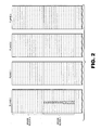
- FIG. 2 A portion of flash memory cell array 15 is shown in FIG. 2 .
- the memory cell array is physically divided into two or more planes, four planes 0 - 3 being illustrated.
- Each plane is a sub-array of memory cells that has its own data registers, sense amplifiers, addressing decoders and the like in order to be able to operate largely independently of the other planes. All the planes may be provided on a single integrated circuit device or on multiple devices, an example being to form each plane from one or more distinct integrated circuit devices.
- Each erase block in the example system of FIG. 2 contains 16 pages P 0 -P 15 , each page having a capacity of one, two or more host data sectors and some overhead data.
- FIG. 3 Another memory arrangement is illustrated in FIG. 3 .
- Each plane contains a large number of erase blocks.
- erase blocks within different planes are logically linked to form metablocks.
- One such metablock is illustrated in FIG. 3 by dashed lines showing logically linked blocks in different planes.
- Each metablock is logically addressable and the memory controller assigns and keeps track of the erase blocks that form the individual metablocks.
- the host system provides data in the form of a stream of sectors. This stream of sectors is divided into logical blocks.
- a logical block is a logical unit of data that contains the same number of sectors of data as are contained in a metablock of the memory array.
- the memory controller maintains a record of the location where each logical block is stored. All blocks of the metablock are erased together, and pages from each block are generally programmed and read simultaneously.
- erase blocks are linked together to form metablocks in a static linking arrangement.
- block 0 of each plane could be linked to form a metablock; block 1 of each plane could be similarly linked to form another metablock, etc.
- erase blocks are linked together in dynamic manner so that different erase blocks may be linked at different times.
- FIG. 4 shows the case of four planes, each in a different memory die (Die A-Die D).
- the shaded areas indicate particular erase blocks in each plane that are to be programmed in parallel as a metablock.
- This allows efficient operation of the memory for mass data storage. For example, when a large amount of data is sent by a host for storage in the memory the data may be stored with a high degree of parallelism. Data may be transferred from the memory controller over the data bus sequentially to on-chip registers (data latches) in each plane. The data may then be written from the registers to the memory array in parallel. Linked blocks forming a metablock may be read in parallel also and data may then be transferred over the shared data bus in series. Linked blocks forming a metablock may also be erased in parallel.
- FIG. 5 shows another example in which two dies (Die A, Die B) are connected to a memory controller and each die has two planes (plane 0 , plane 1 ). The shaded blocks of the four different planes are linked to form a metablock. It will be understood that FIGS. 4 and 5 are simply examples and that many other configurations with different numbers of dies and/or planes are possible. It will also be understood that a memory controller may operate more than one memory bus and each memory bus may have many memory dies and planes. Aspects of the present examples are not limited to any particular number of dies and/or planes.
- blocks are subject to some testing to determine if they meet some minimum standard. Blocks that fail to meet this standard are designated as “bad blocks” and are not subsequently used for data storage. Bad blocks may be detected during an initial testing operation, prior to storing any user data, or may be detected later after some period of use. For example, a block may become bad over time and may be detected by failure to read, write, or erase adequately (e.g. within some predetermined period of time). When bad blocks are found, their locations may be recorded so that there are no subsequent attempts to store data in them. A memory controller may maintain a bad block list for this purpose.
- FIG. 6 illustrates a multi-plane memory system with some bad blocks.
- Plane 0 includes three bad blocks while plane 1 includes just one bad block.
- Bad blocks are mapped out by recording their locations in a bad block list which prevents subsequent storage of user data in the bad blocks.
- Good blocks are configured for parallel operation by linking them into metablocks. However, in this example the number of bad blocks per plane is unequal and accordingly the number of good blocks per plane is unequal.
- each good block in plane 0 is linked to a good block in plane 1 . Because there are more good blocks in plane 1 there are some good blocks in plane 1 that are left over, i.e. some good blocks in plane 1 for which no corresponding good block in plane 0 exists (odd blocks).
- the number of blocks in plane 1 two greater than the number of good blocks in plane 0 so that two odd blocks remain after linking.
- Such odd blocks may remain unused because the memory is configured for parallel operation and the odd blocks are not linked and thus are not configured for parallel operation. This may result in low memory capacity.
- the lost capacity due to odd blocks in addition to capacity lost due to bad blocks, may be significant. In particular, where bad blocks are concentrated in a particular plane or planes and other planes have fewer bad blocks a significant number of otherwise good blocks may go unused simply because no corresponding good blocks are available for linking for parallel operation.
- FIG. 7 shows a four plane arrangement in which capacity is lost in planes 1 - 3 because there are insufficient good blocks in plane 0 to allow all good blocks in planes 1 - 3 to be linked.
- FIG. 7 illustrates lost capacity due to bad blocks (shaded) and odd blocks (hashed) in logical space (bad blocks are not physically located contiguously but capacity lost due to bad blocks may be considered as a single portion of logical space, similarly odd blocks may be at various physical locations and are not necessarily contiguous).
- the amount of space that is configured for parallel operation depends on the number of good blocks in the worst plane (i.e. in the plane with the fewest good blocks) which is plane 0 in this example.
- Remaining good blocks in planes 1 - 3 have no corresponding good block to link with in plane 0 and so remain unlinked. It can be seen that capacity loss due to odd blocks generally increases with the number of planes operated in parallel and varies with the distribution of bad blocks (more capacity lost when bad blocks are concentrated in a plane).
- Odd blocks may be configured for individual operation (not in parallel with a block of another plane). This allows such odd blocks to be used even where no corresponding block is available in another plane.
- long host writes are directed to linked blocks (metablocks) so that such data is written with a high degree of parallelism. This data may subsequently be read with a similarly high degree of parallelism and the linked blocks may be erased in parallel when the data they contain becomes obsolete.
- Short host writes and writes of memory system management data are directed to individual blocks (unlinked blocks) and are written with low parallelism (one plane writes).
- Individually operated blocks may be operated so that adequate access speed is maintained (e.g. by SLC operation). By reserving individual blocks for appropriate data and operating them in an appropriate way, the additional capacity of the individual blocks may be used with little or no impact on overall memory access speeds.
- Memory system management data may include a variety of different types of data that are maintained by a memory controller in a nonvolatile memory. Rather than being received from a host through a host interface, such data is generated by the memory controller and is used in its operation.
- Memory management data may include boot code, file system data, logical-to-physical address mapping data, bad block location data, allocation data, and other types of data that the memory controller may maintain. Different memory systems may differ in how memory system management data is configured and stored.
- Memory management data may all be maintained in the same manner, or different types of memory management data may be maintained in different manners. For example, boot code and bad block location data may be infrequently updated and may be stored in a dedicated block or blocks so that write disturbs are minimized while file system data may be frequently updated and may be stored in different blocks.
- FIG. 8 illustrates a two plane memory array in which all good blocks of the worst plane (plane with fewest good blocks, plane 0 in this example) are operated in parallel for storage of long host writes. Remaining good blocks of plane 1 that are unlinked are configured for individual operation for storage of short host writes and/or memory system management data.
- FIG. 9 illustrates how blocks may be configured for different interleaving (e.g. multi-plane interleaving and single-plane operation).
- the number of good and bad blocks in each plane is determined 901 .
- blocks of different planes are linked until good blocks of at least one plane (plane with smallest number of good blocks) are exhausted 903 .
- any remaining (unlinked) good blocks in other planes are configured for individual operation 905 .
- a memory controller may maintain a record indicating the locations of such individual blocks and may refer to the record when storing data.
- blocks that are operated individually may be operated in a similar manner to blocks that are linked and operated in parallel.
- blocks that are operated individually may be operated differently.
- SLC Single Level Cell
- MLC Multi Level Cell
- Different wear leveling schemes may be applied to linked blocks and individually operated blocks. Data access patterns may be very different causing these blocks to wear very differently.
- linked blocks used for storage of long host writes may have low wear (low write-erase cycle count) because such data may be stored for relatively long periods of time.
- individually operated blocks that are used for short host writes and/or memory management data may be frequently written and erased especially if there are few such blocks so that wear leveling becomes more important and may be more frequently performed. Operating such blocks in SLC mode may help to reduce wear. In some cases, it may be desirable to remap blocks for linked and individual operation after some period of time or some threshold number of write erase cycles.
- blocks that were initially linked may be unlinked and subsequently operated individually while blocks that were initially individually operated may subsequently be linked for parallel operation.
- the pool of individually operated blocks may contain the same number of blocks over time, the physical blocks in the pool may be rotated over time in order to promote wear leveling.
- FIG. 10 illustrates configuration of blocks of a multi-plane memory array.
- Linked blocks are configured for MLC or SLC operation 111 (e.g. storing one, two, three, or more bits per memory cell).
- linked SLC blocks are used to provide high speed writing of data received from a host and the data is later relocated to linked MLC blocks.
- a specific wear leveling scheme is applied to such linked MLC and SLC blocks 113 .
- Individually operated blocks are configured for SLC operation 115 in this example.
- a specific wear leveling scheme is applied to such individually operated blocks 117 . In other examples, some or all individually operated blocks may be operated as MLC blocks.
- individually operated blocks may be operated in a variety of ways to achieve desired results.
- individually operated blocks use particular schemes that are not used in linked blocks to ensure that important data is protected from loss.
- some memory management data may be considered to be important because if it was lost then the operation of the memory could be compromised.
- more than one copy of some memory management data may be stored in individually operated blocks (while only one copy of host data may be stored in linked blocks). For example two copies of boot code may be maintained.
- Different ECC schemes may be applied to data in linked blocks and individually operated blocks.
- MLC data has a higher Bit Error Rate (BER) than SLC data in similar blocks so that MLC data may require greater ECC redundancy.
- BER Bit Error Rate
- ECC redundancy is applied to memory management data to provide a high degree of protection from loss.
- Other redundancy schemes such as applying Exclusive OR (XOR) schemes, may be used to ensure that important data can be recovered.
- XOR Exclusive OR
- certain physical locations in three dimensional blocks may produce higher Bit Error Rates (BERs). For example, memory cells in lower physical levels (closer to the substrate) or along edges of blocks may have higher BERs. Storage of certain memory management data in such physical locations may be prohibited even where storage of host data in such locations in linked blocks is permitted.
- FIG. 11 illustrates an example of how data may be stored in a multi-plane memory that uses different interleave schemes.
- a determination may be made as to whether the data is memory management data 119 . If it is memory management data then it is stored in individual blocks that are operated in SLC format 121 . If the data is not memory management data then a determination is made as to whether the data is host data greater than a threshold amount 123 . The threshold may be based on the page size (i.e. on the amount of data that may be written in one block in a given write operation) or other memory parameter. If the host data exceeds the threshold amount then the data is stored in one or more metablocks 125 (linked blocks across multiple planes). Metablocks may use SLC or MLC format.
- the data may initially be stored in an SLC metablock and later relocated to an MLC metablock (in a “folding” operation) so that high write speed and high long-term storage density are achieved. If the host data is not greater than the threshold amount then the host data is stored in individually operated blocks in SLC format 121 .
- bad blocks develop over time so that a block that is initially good may subsequently become bad (a “grown” bad block). This may affect operation of linked blocks. For example, where one block in a metablock becomes bad then the metablock can no longer be operated. The remaining good block or blocks from the metablock may then be unlinked and reconfigured so that they remain in use.
- FIG. 12 shows an example in which a new bad block 231 develops in the plane with the fewest good blocks, plane 0 . This further reduces the number of good blocks in plane 0 and thus reduces the number of metablocks that can be formed. Accordingly, good block 233 in plane 1 (previously linked to new bad block 231 ) is unlinked from new bad block 231 and is configured for individual operation.
- FIG. 13 shows an example in which a new bad block 335 develops in a plane 1 which is not the plane with the fewest good blocks.
- new bad block 335 in plane 1 may be unlinked and the corresponding good block 337 in plane 0 may be linked to a different block of plane 1 .
- the number of good blocks in plane 0 remains as before, the number of metablocks may be kept the same by relinking good block 337 with a block in plane 1 that was previously individually operated. While this may reduce the number of individually operated blocks in plane 1 it maintains the number of metablocks.
- Another possibility is that a block that is configured for individual operation becomes bad. In this case, no change in block linking is required. The block simply becomes a bad block and the number of individual blocks is reduced accordingly.
- the number of individually operated blocks resulting from unequal numbers of bad blocks in different planes is not sufficient to store short host writes and memory management data.
- an appropriate modification of the above schemes may be applied. For example some short host writes, or some memory management data may be stored in parallel in MLC blocks, or some blocks may be unlinked and operated independently even where there are corresponding blocks across all planes to allow block linking.
Landscapes
- Engineering & Computer Science (AREA)
- Theoretical Computer Science (AREA)
- Physics & Mathematics (AREA)
- General Engineering & Computer Science (AREA)
- General Physics & Mathematics (AREA)
- Human Computer Interaction (AREA)
- Techniques For Improving Reliability Of Storages (AREA)
- Read Only Memory (AREA)
Abstract
Description
Claims (20)
Priority Applications (1)
| Application Number | Priority Date | Filing Date | Title |
|---|---|---|---|
| US14/488,037 US10114562B2 (en) | 2014-09-16 | 2014-09-16 | Adaptive block allocation in nonvolatile memory |
Applications Claiming Priority (1)
| Application Number | Priority Date | Filing Date | Title |
|---|---|---|---|
| US14/488,037 US10114562B2 (en) | 2014-09-16 | 2014-09-16 | Adaptive block allocation in nonvolatile memory |
Publications (2)
| Publication Number | Publication Date |
|---|---|
| US20160077749A1 US20160077749A1 (en) | 2016-03-17 |
| US10114562B2 true US10114562B2 (en) | 2018-10-30 |
Family
ID=55454791
Family Applications (1)
| Application Number | Title | Priority Date | Filing Date |
|---|---|---|---|
| US14/488,037 Active 2035-06-11 US10114562B2 (en) | 2014-09-16 | 2014-09-16 | Adaptive block allocation in nonvolatile memory |
Country Status (1)
| Country | Link |
|---|---|
| US (1) | US10114562B2 (en) |
Cited By (2)
| Publication number | Priority date | Publication date | Assignee | Title |
|---|---|---|---|---|
| US11733921B2 (en) | 2020-10-26 | 2023-08-22 | SK Hynix Inc. | Memory device and memory system including the same |
| US12014781B2 (en) | 2020-10-26 | 2024-06-18 | SK Hynix Inc. | Memory device supporting interleaved operations and memory system including the same |
Families Citing this family (59)
| Publication number | Priority date | Publication date | Assignee | Title |
|---|---|---|---|---|
| US10566040B2 (en) | 2016-07-29 | 2020-02-18 | Micron Technology, Inc. | Variable page size architecture |
| US10223022B2 (en) * | 2017-01-27 | 2019-03-05 | Western Digital Technologies, Inc. | System and method for implementing super word line zones in a memory device |
| US10497447B2 (en) * | 2017-06-29 | 2019-12-03 | SK Hynix Inc. | Memory device capable of supporting multiple read operations |
| TWI653632B (en) * | 2017-09-29 | 2019-03-11 | 群聯電子股份有限公司 | Memory management method, memory control circuit unit and memory storage device |
| CN108256103B (en) * | 2018-02-05 | 2019-02-05 | 清华大学 | A method and system for capacity expansion based on double-layer list structure |
| US10496548B2 (en) | 2018-02-07 | 2019-12-03 | Alibaba Group Holding Limited | Method and system for user-space storage I/O stack with user-space flash translation layer |
| CN110489051A (en) * | 2018-05-14 | 2019-11-22 | 慧荣科技股份有限公司 | The programmed method of data memory device and system information |
| US11379155B2 (en) | 2018-05-24 | 2022-07-05 | Alibaba Group Holding Limited | System and method for flash storage management using multiple open page stripes |
| CN108733324B (en) * | 2018-05-25 | 2021-11-09 | 郑州云海信息技术有限公司 | Data reading and writing method, device and equipment of solid state disk and storage medium |
| WO2020000136A1 (en) | 2018-06-25 | 2020-01-02 | Alibaba Group Holding Limited | System and method for managing resources of a storage device and quantifying the cost of i/o requests |
| US10921992B2 (en) | 2018-06-25 | 2021-02-16 | Alibaba Group Holding Limited | Method and system for data placement in a hard disk drive based on access frequency for improved IOPS and utilization efficiency |
| US20200042223A1 (en) * | 2018-08-02 | 2020-02-06 | Alibaba Group Holding Limited | System and method for facilitating a high-density storage device with improved performance and endurance |
| US10996886B2 (en) | 2018-08-02 | 2021-05-04 | Alibaba Group Holding Limited | Method and system for facilitating atomicity and latency assurance on variable sized I/O |
| KR102533207B1 (en) * | 2018-08-30 | 2023-05-17 | 에스케이하이닉스 주식회사 | Data Storage Device and Operation Method Thereof, Storage System Having the Same |
| US11327929B2 (en) | 2018-09-17 | 2022-05-10 | Alibaba Group Holding Limited | Method and system for reduced data movement compression using in-storage computing and a customized file system |
| US10553290B1 (en) * | 2018-10-30 | 2020-02-04 | Micron Technology, Inc. | Read disturb scan consolidation |
| KR102592803B1 (en) * | 2018-10-31 | 2023-10-24 | 에스케이하이닉스 주식회사 | Data storage device and operating method thereof |
| US10977122B2 (en) | 2018-12-31 | 2021-04-13 | Alibaba Group Holding Limited | System and method for facilitating differentiated error correction in high-density flash devices |
| US11061735B2 (en) | 2019-01-02 | 2021-07-13 | Alibaba Group Holding Limited | System and method for offloading computation to storage nodes in distributed system |
| US11132291B2 (en) | 2019-01-04 | 2021-09-28 | Alibaba Group Holding Limited | System and method of FPGA-executed flash translation layer in multiple solid state drives |
| US11561834B2 (en) * | 2019-01-16 | 2023-01-24 | Rambus Inc. | Methods and systems for adaptive memory-resource management |
| US11200337B2 (en) | 2019-02-11 | 2021-12-14 | Alibaba Group Holding Limited | System and method for user data isolation |
| US10860223B1 (en) | 2019-07-18 | 2020-12-08 | Alibaba Group Holding Limited | Method and system for enhancing a distributed storage system by decoupling computation and network tasks |
| US11617282B2 (en) | 2019-10-01 | 2023-03-28 | Alibaba Group Holding Limited | System and method for reshaping power budget of cabinet to facilitate improved deployment density of servers |
| US11126561B2 (en) | 2019-10-01 | 2021-09-21 | Alibaba Group Holding Limited | Method and system for organizing NAND blocks and placing data to facilitate high-throughput for random writes in a solid state drive |
| US11573891B2 (en) | 2019-11-25 | 2023-02-07 | SK Hynix Inc. | Memory controller for scheduling commands based on response for receiving write command, storage device including the memory controller, and operating method of the memory controller and the storage device |
| KR102456176B1 (en) * | 2020-05-21 | 2022-10-19 | 에스케이하이닉스 주식회사 | Memory controller and operating method thereof |
| US11449455B2 (en) | 2020-01-15 | 2022-09-20 | Alibaba Group Holding Limited | Method and system for facilitating a high-capacity object storage system with configuration agility and mixed deployment flexibility |
| TWI751482B (en) * | 2020-01-22 | 2022-01-01 | 宏碁股份有限公司 | Data writing method and storage controller |
| US11379447B2 (en) | 2020-02-06 | 2022-07-05 | Alibaba Group Holding Limited | Method and system for enhancing IOPS of a hard disk drive system based on storing metadata in host volatile memory and data in non-volatile memory using a shared controller |
| US11150986B2 (en) | 2020-02-26 | 2021-10-19 | Alibaba Group Holding Limited | Efficient compaction on log-structured distributed file system using erasure coding for resource consumption reduction |
| US11200114B2 (en) | 2020-03-17 | 2021-12-14 | Alibaba Group Holding Limited | System and method for facilitating elastic error correction code in memory |
| US11449386B2 (en) | 2020-03-20 | 2022-09-20 | Alibaba Group Holding Limited | Method and system for optimizing persistent memory on data retention, endurance, and performance for host memory |
| US11169881B2 (en) | 2020-03-30 | 2021-11-09 | Alibaba Group Holding Limited | System and method for facilitating reduction of complexity and data movement in erasure coding merging on journal and data storage drive |
| CN113515230B (en) * | 2020-04-10 | 2023-11-14 | 宏碁股份有限公司 | Data writing method and storage controller |
| US11301173B2 (en) | 2020-04-20 | 2022-04-12 | Alibaba Group Holding Limited | Method and system for facilitating evaluation of data access frequency and allocation of storage device resources |
| US11385833B2 (en) | 2020-04-20 | 2022-07-12 | Alibaba Group Holding Limited | Method and system for facilitating a light-weight garbage collection with a reduced utilization of resources |
| US11281575B2 (en) | 2020-05-11 | 2022-03-22 | Alibaba Group Holding Limited | Method and system for facilitating data placement and control of physical addresses with multi-queue I/O blocks |
| US11494115B2 (en) | 2020-05-13 | 2022-11-08 | Alibaba Group Holding Limited | System method for facilitating memory media as file storage device based on real-time hashing by performing integrity check with a cyclical redundancy check (CRC) |
| US11461262B2 (en) | 2020-05-13 | 2022-10-04 | Alibaba Group Holding Limited | Method and system for facilitating a converged computation and storage node in a distributed storage system |
| US11218165B2 (en) | 2020-05-15 | 2022-01-04 | Alibaba Group Holding Limited | Memory-mapped two-dimensional error correction code for multi-bit error tolerance in DRAM |
| US11507499B2 (en) | 2020-05-19 | 2022-11-22 | Alibaba Group Holding Limited | System and method for facilitating mitigation of read/write amplification in data compression |
| US11556277B2 (en) | 2020-05-19 | 2023-01-17 | Alibaba Group Holding Limited | System and method for facilitating improved performance in ordering key-value storage with input/output stack simplification |
| US11263132B2 (en) | 2020-06-11 | 2022-03-01 | Alibaba Group Holding Limited | Method and system for facilitating log-structure data organization |
| US11354200B2 (en) | 2020-06-17 | 2022-06-07 | Alibaba Group Holding Limited | Method and system for facilitating data recovery and version rollback in a storage device |
| US11422931B2 (en) | 2020-06-17 | 2022-08-23 | Alibaba Group Holding Limited | Method and system for facilitating a physically isolated storage unit for multi-tenancy virtualization |
| US11354233B2 (en) | 2020-07-27 | 2022-06-07 | Alibaba Group Holding Limited | Method and system for facilitating fast crash recovery in a storage device |
| US11372774B2 (en) | 2020-08-24 | 2022-06-28 | Alibaba Group Holding Limited | Method and system for a solid state drive with on-chip memory integration |
| US11487465B2 (en) | 2020-12-11 | 2022-11-01 | Alibaba Group Holding Limited | Method and system for a local storage engine collaborating with a solid state drive controller |
| US11734115B2 (en) | 2020-12-28 | 2023-08-22 | Alibaba Group Holding Limited | Method and system for facilitating write latency reduction in a queue depth of one scenario |
| CN114691016A (en) * | 2020-12-29 | 2022-07-01 | 深圳市江波龙电子股份有限公司 | Equipment capacity configuration method and device, terminal equipment and storage medium |
| US11416365B2 (en) | 2020-12-30 | 2022-08-16 | Alibaba Group Holding Limited | Method and system for open NAND block detection and correction in an open-channel SSD |
| US11726699B2 (en) | 2021-03-30 | 2023-08-15 | Alibaba Singapore Holding Private Limited | Method and system for facilitating multi-stream sequential read performance improvement with reduced read amplification |
| US11461173B1 (en) | 2021-04-21 | 2022-10-04 | Alibaba Singapore Holding Private Limited | Method and system for facilitating efficient data compression based on error correction code and reorganization of data placement |
| US11476874B1 (en) | 2021-05-14 | 2022-10-18 | Alibaba Singapore Holding Private Limited | Method and system for facilitating a storage server with hybrid memory for journaling and data storage |
| US20230266910A1 (en) * | 2022-02-22 | 2023-08-24 | Intel NDTM US LLC | Method and apparatus to select a plane in a nand flash die to store a read-only reserved block |
| KR20240058593A (en) * | 2022-10-26 | 2024-05-07 | 에스케이하이닉스 주식회사 | Memory system and operating method of memory system |
| CN118502645A (en) * | 2023-02-16 | 2024-08-16 | 长江存储科技有限责任公司 | Memory system and method of operating the same |
| US12292796B2 (en) * | 2023-04-28 | 2025-05-06 | SanDisk Technologies, Inc. | Data storage device and method for performance-dependent storage of parity information |
Citations (78)
| Publication number | Priority date | Publication date | Assignee | Title |
|---|---|---|---|---|
| US5043940A (en) | 1988-06-08 | 1991-08-27 | Eliyahou Harari | Flash EEPROM memory systems having multistate storage cells |
| US5070032A (en) | 1989-03-15 | 1991-12-03 | Sundisk Corporation | Method of making dense flash eeprom semiconductor memory structures |
| US5095344A (en) | 1988-06-08 | 1992-03-10 | Eliyahou Harari | Highly compact eprom and flash eeprom devices |
| US5172338A (en) | 1989-04-13 | 1992-12-15 | Sundisk Corporation | Multi-state EEprom read and write circuits and techniques |
| JPH05314019A (en) | 1992-05-08 | 1993-11-26 | Toshiba Corp | Memory card device |
| US5313421A (en) | 1992-01-14 | 1994-05-17 | Sundisk Corporation | EEPROM with split gate source side injection |
| US5315541A (en) | 1992-07-24 | 1994-05-24 | Sundisk Corporation | Segmented column memory array |
| US5343063A (en) | 1990-12-18 | 1994-08-30 | Sundisk Corporation | Dense vertical programmable read only memory cell structure and processes for making them |
| US5367484A (en) | 1993-04-01 | 1994-11-22 | Microchip Technology Incorporated | Programmable high endurance block for EEPROM device |
| US5404485A (en) | 1993-03-08 | 1995-04-04 | M-Systems Flash Disk Pioneers Ltd. | Flash file system |
| US5473765A (en) | 1994-01-24 | 1995-12-05 | 3Com Corporation | Apparatus for using flash memory as a floppy disk emulator in a computer system |
| US5532962A (en) | 1992-05-20 | 1996-07-02 | Sandisk Corporation | Soft errors handling in EEPROM devices |
| US5570315A (en) | 1993-09-21 | 1996-10-29 | Kabushiki Kaisha Toshiba | Multi-state EEPROM having write-verify control circuit |
| US5661053A (en) | 1994-05-25 | 1997-08-26 | Sandisk Corporation | Method of making dense flash EEPROM cell array and peripheral supporting circuits formed in deposited field oxide with the use of spacers |
| US5742934A (en) | 1995-09-13 | 1998-04-21 | Mitsubishi Denki Kabushiki Kaisha | Flash solid state disk card with selective use of an address conversion table depending on logical and physical sector numbers |
| US5751634A (en) | 1995-05-16 | 1998-05-12 | Kabushiki Kaisha Toshiba | Non-volatile semiconductor memory device for storing multivalue data and readout/write-in method therefor |
| US5768192A (en) | 1996-07-23 | 1998-06-16 | Saifun Semiconductors, Ltd. | Non-volatile semiconductor memory cell utilizing asymmetrical charge trapping |
| US5774397A (en) | 1993-06-29 | 1998-06-30 | Kabushiki Kaisha Toshiba | Non-volatile semiconductor memory device and method of programming a non-volatile memory cell to a predetermined state |
| US5798968A (en) | 1996-09-24 | 1998-08-25 | Sandisk Corporation | Plane decode/virtual sector architecture |
| EP0887732A1 (en) | 1997-06-20 | 1998-12-30 | Sony Corporation | Defective management data handling method and recording medium |
| US5860124A (en) | 1996-09-30 | 1999-01-12 | Intel Corporation | Method for performing a continuous over-write of a file in nonvolatile memory |
| US5890192A (en) | 1996-11-05 | 1999-03-30 | Sandisk Corporation | Concurrent write of multiple chunks of data into multiple subarrays of flash EEPROM |
| US5903495A (en) | 1996-03-18 | 1999-05-11 | Kabushiki Kaisha Toshiba | Semiconductor device and memory system |
| US5907856A (en) | 1995-07-31 | 1999-05-25 | Lexar Media, Inc. | Moving sectors within a block of information in a flash memory mass storage architecture |
| US5909449A (en) | 1997-09-08 | 1999-06-01 | Invox Technology | Multibit-per-cell non-volatile memory with error detection and correction |
| US5930167A (en) | 1997-07-30 | 1999-07-27 | Sandisk Corporation | Multi-state non-volatile flash memory capable of being its own two state write cache |
| US5937425A (en) | 1997-10-16 | 1999-08-10 | M-Systems Flash Disk Pioneers Ltd. | Flash file system optimized for page-mode flash technologies |
| US6011725A (en) | 1997-08-01 | 2000-01-04 | Saifun Semiconductors, Ltd. | Two bit non-volatile electrically erasable and programmable semiconductor memory cell utilizing asymmetrical charge trapping |
| EP0977121A2 (en) | 1998-07-28 | 2000-02-02 | Sony Corporation | Non-volatile memory, recording apparatus and recording method |
| US6034897A (en) | 1999-04-01 | 2000-03-07 | Lexar Media, Inc. | Space management for managing high capacity nonvolatile memory |
| WO2000049488A1 (en) | 1999-02-17 | 2000-08-24 | Memory Corporation Plc | Memory system |
| US6125435A (en) | 1995-09-13 | 2000-09-26 | Lexar Media, Inc. | Alignment of cluster address to block addresses within a semiconductor non-volatile mass storage memory |
| US6141249A (en) | 1999-04-01 | 2000-10-31 | Lexar Media, Inc. | Organization of blocks within a nonvolatile memory unit to effectively decrease sector write operation time |
| US6222762B1 (en) | 1992-01-14 | 2001-04-24 | Sandisk Corporation | Multi-state memory |
| US6226728B1 (en) | 1998-04-21 | 2001-05-01 | Intel Corporation | Dynamic allocation for efficient management of variable sized data within a nonvolatile memory |
| US6272610B1 (en) | 1993-03-11 | 2001-08-07 | Hitachi, Ltd. | File memory device using flash memories, and an information processing system using the same |
| US6304980B1 (en) | 1996-03-13 | 2001-10-16 | International Business Machines Corporation | Peer-to-peer backup system with failure-triggered device switching honoring reservation of primary device |
| US20010042882A1 (en) | 1999-10-08 | 2001-11-22 | Yun Chang | Method for forming a flash memory cell having contoured floating gate surface |
| US6377500B1 (en) | 1999-11-11 | 2002-04-23 | Kabushiki Kaisha Toshiba | Memory system with a non-volatile memory, having address translating function |
| US6401160B1 (en) | 1999-03-31 | 2002-06-04 | Intel Corporation | Method and apparatus to permit adjustable code/data boundary in a nonvolatile memory |
| US6421279B1 (en) | 1993-04-08 | 2002-07-16 | Hitachi, Ltd. | Flash memory control method and apparatus processing system therewith |
| US20020099904A1 (en) | 2001-01-19 | 2002-07-25 | Conley Kevin M. | Partial block data programming and reading operations in a non-volatile memory |
| US6426893B1 (en) | 2000-02-17 | 2002-07-30 | Sandisk Corporation | Flash eeprom system with simultaneous multiple data sector programming and storage of physical block characteristics in other designated blocks |
| US6456528B1 (en) | 2001-09-17 | 2002-09-24 | Sandisk Corporation | Selective operation of a multi-state non-volatile memory system in a binary mode |
| US6490649B2 (en) | 1998-11-10 | 2002-12-03 | Lexar Media, Inc. | Memory device |
| US6522580B2 (en) | 2001-06-27 | 2003-02-18 | Sandisk Corporation | Operating techniques for reducing effects of coupling between storage elements of a non-volatile memory operated in multiple data states |
| US20030053334A1 (en) | 2001-09-17 | 2003-03-20 | Sandisk Corporation | Selective operation of a multi-state non-volatile memory system in a a binary mode |
| US20030065899A1 (en) | 2001-09-28 | 2003-04-03 | Gorobets Sergey Anatolievich | Memory system sectors |
| WO2003027828A1 (en) | 2001-09-28 | 2003-04-03 | Lexar Media, Inc. | Method of writing data to non-volatile memory |
| WO2003029951A2 (en) | 2001-09-28 | 2003-04-10 | Lexar Media, Inc. | Non-volatile memory control |
| US20030076709A1 (en) | 2001-10-24 | 2003-04-24 | Jen-Ren Huang | Method for operating a multi-level memory cell |
| US6563734B2 (en) | 2000-08-30 | 2003-05-13 | Sharp Kabushiki Kaisha | Non-volatile semiconductor memory device capable of executing erasable, writable and readable functions simultaneously |
| US6567307B1 (en) | 2000-07-21 | 2003-05-20 | Lexar Media, Inc. | Block management for mass storage |
| US6571261B1 (en) | 2000-07-13 | 2003-05-27 | International Business Machines Corporation | Defragmentation utility for a shared disk parallel file system across a storage area network |
| US20030110343A1 (en) | 2001-12-11 | 2003-06-12 | Mitsubishi Denki Kabushiki Kaisha | File system including non-volatile semiconductor memory device having a plurality of banks |
| US20030109093A1 (en) | 2001-10-31 | 2003-06-12 | Eliyahou Harari | Multi-state non-volatile integrated circuit memory systems that employ dielectric storage elements |
| US6591330B2 (en) | 2001-06-18 | 2003-07-08 | M-Systems Flash Disk Pioneers Ltd. | System and method for flexible flash file |
| US20040030825A1 (en) | 2000-10-26 | 2004-02-12 | Toshihiko Otake | Storing device, storing control method and program |
| WO2004040578A2 (en) | 2002-10-28 | 2004-05-13 | Sandisk Corporation | Wear leveling in non-volatile storage systems |
| WO2004040457A1 (en) | 2002-10-28 | 2004-05-13 | Sandisk Corporation | Method and apparatus for managing an erase count block |
| WO2004040459A1 (en) | 2002-10-28 | 2004-05-13 | Sandisk Corporation | Tracking the least frequently erased blocks in non-volatile memory systems |
| WO2004040458A1 (en) | 2002-10-28 | 2004-05-13 | Sandisk Corporation | Maintaining erase counts in non-volatile storage systems |
| US20040103241A1 (en) | 2002-10-28 | 2004-05-27 | Sandisk Corporation | Method and apparatus for effectively enabling an out of sequence write process within a non-volatile memory system |
| EP1424631A1 (en) | 2002-10-28 | 2004-06-02 | SanDisk Corporation | Hybrid implementation for error correction codes within a non-volatile memory system |
| US6895464B2 (en) | 2002-06-03 | 2005-05-17 | Honeywell International Inc. | Flash memory management system and method utilizing multiple block list windows |
| US20050144363A1 (en) | 2003-12-30 | 2005-06-30 | Sinclair Alan W. | Data boundary management |
| US20050144365A1 (en) | 2003-12-30 | 2005-06-30 | Sergey Anatolievich Gorobets | Non-volatile memory and method with control data management |
| US20050144367A1 (en) | 2003-12-30 | 2005-06-30 | Sinclair Alan W. | Data run programming |
| US20050144358A1 (en) | 2003-12-30 | 2005-06-30 | Conley Kevin M. | Management of non-volatile memory systems having large erase blocks |
| US20050286297A1 (en) * | 2004-06-25 | 2005-12-29 | Micron Technology, Inc. | Multiple level cell memory device with single bit per cell, re-mappable memory block |
| US6988175B2 (en) | 2003-06-30 | 2006-01-17 | M-Systems Flash Disk Pioneers Ltd. | Flash memory management method that is resistant to data corruption by power loss |
| US7032065B2 (en) | 2000-11-22 | 2006-04-18 | Sandisk Corporation | Techniques for operating non-volatile memory systems with data sectors having different sizes than the sizes of the pages and/or blocks of the memory |
| US7315916B2 (en) | 2004-12-16 | 2008-01-01 | Sandisk Corporation | Scratch pad block |
| US20090240873A1 (en) * | 2003-12-02 | 2009-09-24 | Super Talent Electronics Inc. | Multi-Level Striping and Truncation Channel-Equalization for Flash-Memory System |
| US20100169540A1 (en) * | 2008-12-30 | 2010-07-01 | Sinclair Alan W | Method and apparatus for relocating selected data between flash partitions in a memory device |
| US20110271043A1 (en) * | 2010-04-29 | 2011-11-03 | Avigdor Segal | System and method for allocating and using spare blocks in a flash memory |
| US20130024605A1 (en) * | 2011-07-22 | 2013-01-24 | Sandisk Technologies Inc. | Systems and methods of storing data |
| JP5314019B2 (en) | 2007-08-01 | 2013-10-16 | キャボット マイクロエレクトロニクス コーポレイション | Ruthenium CMP composition and method |
-
2014
- 2014-09-16 US US14/488,037 patent/US10114562B2/en active Active
Patent Citations (92)
| Publication number | Priority date | Publication date | Assignee | Title |
|---|---|---|---|---|
| US5095344A (en) | 1988-06-08 | 1992-03-10 | Eliyahou Harari | Highly compact eprom and flash eeprom devices |
| US5043940A (en) | 1988-06-08 | 1991-08-27 | Eliyahou Harari | Flash EEPROM memory systems having multistate storage cells |
| US5070032A (en) | 1989-03-15 | 1991-12-03 | Sundisk Corporation | Method of making dense flash eeprom semiconductor memory structures |
| US5172338A (en) | 1989-04-13 | 1992-12-15 | Sundisk Corporation | Multi-state EEprom read and write circuits and techniques |
| US5172338B1 (en) | 1989-04-13 | 1997-07-08 | Sandisk Corp | Multi-state eeprom read and write circuits and techniques |
| US5343063A (en) | 1990-12-18 | 1994-08-30 | Sundisk Corporation | Dense vertical programmable read only memory cell structure and processes for making them |
| US6222762B1 (en) | 1992-01-14 | 2001-04-24 | Sandisk Corporation | Multi-state memory |
| US5313421A (en) | 1992-01-14 | 1994-05-17 | Sundisk Corporation | EEPROM with split gate source side injection |
| JPH05314019A (en) | 1992-05-08 | 1993-11-26 | Toshiba Corp | Memory card device |
| US5532962A (en) | 1992-05-20 | 1996-07-02 | Sandisk Corporation | Soft errors handling in EEPROM devices |
| US5315541A (en) | 1992-07-24 | 1994-05-24 | Sundisk Corporation | Segmented column memory array |
| US5404485A (en) | 1993-03-08 | 1995-04-04 | M-Systems Flash Disk Pioneers Ltd. | Flash file system |
| US6272610B1 (en) | 1993-03-11 | 2001-08-07 | Hitachi, Ltd. | File memory device using flash memories, and an information processing system using the same |
| US5367484A (en) | 1993-04-01 | 1994-11-22 | Microchip Technology Incorporated | Programmable high endurance block for EEPROM device |
| US6421279B1 (en) | 1993-04-08 | 2002-07-16 | Hitachi, Ltd. | Flash memory control method and apparatus processing system therewith |
| US5774397A (en) | 1993-06-29 | 1998-06-30 | Kabushiki Kaisha Toshiba | Non-volatile semiconductor memory device and method of programming a non-volatile memory cell to a predetermined state |
| US5570315A (en) | 1993-09-21 | 1996-10-29 | Kabushiki Kaisha Toshiba | Multi-state EEPROM having write-verify control circuit |
| US5473765A (en) | 1994-01-24 | 1995-12-05 | 3Com Corporation | Apparatus for using flash memory as a floppy disk emulator in a computer system |
| US5661053A (en) | 1994-05-25 | 1997-08-26 | Sandisk Corporation | Method of making dense flash EEPROM cell array and peripheral supporting circuits formed in deposited field oxide with the use of spacers |
| US5751634A (en) | 1995-05-16 | 1998-05-12 | Kabushiki Kaisha Toshiba | Non-volatile semiconductor memory device for storing multivalue data and readout/write-in method therefor |
| US5907856A (en) | 1995-07-31 | 1999-05-25 | Lexar Media, Inc. | Moving sectors within a block of information in a flash memory mass storage architecture |
| US5742934A (en) | 1995-09-13 | 1998-04-21 | Mitsubishi Denki Kabushiki Kaisha | Flash solid state disk card with selective use of an address conversion table depending on logical and physical sector numbers |
| US6125435A (en) | 1995-09-13 | 2000-09-26 | Lexar Media, Inc. | Alignment of cluster address to block addresses within a semiconductor non-volatile mass storage memory |
| US6304980B1 (en) | 1996-03-13 | 2001-10-16 | International Business Machines Corporation | Peer-to-peer backup system with failure-triggered device switching honoring reservation of primary device |
| US6046935A (en) | 1996-03-18 | 2000-04-04 | Kabushiki Kaisha Toshiba | Semiconductor device and memory system |
| US5903495A (en) | 1996-03-18 | 1999-05-11 | Kabushiki Kaisha Toshiba | Semiconductor device and memory system |
| US5768192A (en) | 1996-07-23 | 1998-06-16 | Saifun Semiconductors, Ltd. | Non-volatile semiconductor memory cell utilizing asymmetrical charge trapping |
| US5798968A (en) | 1996-09-24 | 1998-08-25 | Sandisk Corporation | Plane decode/virtual sector architecture |
| US5860124A (en) | 1996-09-30 | 1999-01-12 | Intel Corporation | Method for performing a continuous over-write of a file in nonvolatile memory |
| US6542956B1 (en) | 1996-11-05 | 2003-04-01 | Sandisk Corporation | Latched address multi-chunk write to EEPROM |
| US5890192A (en) | 1996-11-05 | 1999-03-30 | Sandisk Corporation | Concurrent write of multiple chunks of data into multiple subarrays of flash EEPROM |
| EP0887732A1 (en) | 1997-06-20 | 1998-12-30 | Sony Corporation | Defective management data handling method and recording medium |
| US5930167A (en) | 1997-07-30 | 1999-07-27 | Sandisk Corporation | Multi-state non-volatile flash memory capable of being its own two state write cache |
| US6011725A (en) | 1997-08-01 | 2000-01-04 | Saifun Semiconductors, Ltd. | Two bit non-volatile electrically erasable and programmable semiconductor memory cell utilizing asymmetrical charge trapping |
| US5909449A (en) | 1997-09-08 | 1999-06-01 | Invox Technology | Multibit-per-cell non-volatile memory with error detection and correction |
| US5937425A (en) | 1997-10-16 | 1999-08-10 | M-Systems Flash Disk Pioneers Ltd. | Flash file system optimized for page-mode flash technologies |
| US6226728B1 (en) | 1998-04-21 | 2001-05-01 | Intel Corporation | Dynamic allocation for efficient management of variable sized data within a nonvolatile memory |
| EP0977121A2 (en) | 1998-07-28 | 2000-02-02 | Sony Corporation | Non-volatile memory, recording apparatus and recording method |
| US6490649B2 (en) | 1998-11-10 | 2002-12-03 | Lexar Media, Inc. | Memory device |
| US6725321B1 (en) | 1999-02-17 | 2004-04-20 | Lexar Media, Inc. | Memory system |
| WO2000049488A1 (en) | 1999-02-17 | 2000-08-24 | Memory Corporation Plc | Memory system |
| US6401160B1 (en) | 1999-03-31 | 2002-06-04 | Intel Corporation | Method and apparatus to permit adjustable code/data boundary in a nonvolatile memory |
| US6141249A (en) | 1999-04-01 | 2000-10-31 | Lexar Media, Inc. | Organization of blocks within a nonvolatile memory unit to effectively decrease sector write operation time |
| US6034897A (en) | 1999-04-01 | 2000-03-07 | Lexar Media, Inc. | Space management for managing high capacity nonvolatile memory |
| WO2001018640A1 (en) | 1999-09-03 | 2001-03-15 | Lexar Media, Inc. | Organization of blocks within a nonvolatile memory unit to effectively decrease sector write operation time |
| US20010042882A1 (en) | 1999-10-08 | 2001-11-22 | Yun Chang | Method for forming a flash memory cell having contoured floating gate surface |
| US6377500B1 (en) | 1999-11-11 | 2002-04-23 | Kabushiki Kaisha Toshiba | Memory system with a non-volatile memory, having address translating function |
| US6426893B1 (en) | 2000-02-17 | 2002-07-30 | Sandisk Corporation | Flash eeprom system with simultaneous multiple data sector programming and storage of physical block characteristics in other designated blocks |
| US6571261B1 (en) | 2000-07-13 | 2003-05-27 | International Business Machines Corporation | Defragmentation utility for a shared disk parallel file system across a storage area network |
| US6567307B1 (en) | 2000-07-21 | 2003-05-20 | Lexar Media, Inc. | Block management for mass storage |
| US6563734B2 (en) | 2000-08-30 | 2003-05-13 | Sharp Kabushiki Kaisha | Non-volatile semiconductor memory device capable of executing erasable, writable and readable functions simultaneously |
| US20040030825A1 (en) | 2000-10-26 | 2004-02-12 | Toshihiko Otake | Storing device, storing control method and program |
| US7032065B2 (en) | 2000-11-22 | 2006-04-18 | Sandisk Corporation | Techniques for operating non-volatile memory systems with data sectors having different sizes than the sizes of the pages and/or blocks of the memory |
| WO2002058074A2 (en) | 2001-01-19 | 2002-07-25 | Sandisk Corporation | Partial block data programming and reading operations in a non-volatile memory |
| US6763424B2 (en) | 2001-01-19 | 2004-07-13 | Sandisk Corporation | Partial block data programming and reading operations in a non-volatile memory |
| US20020099904A1 (en) | 2001-01-19 | 2002-07-25 | Conley Kevin M. | Partial block data programming and reading operations in a non-volatile memory |
| US6591330B2 (en) | 2001-06-18 | 2003-07-08 | M-Systems Flash Disk Pioneers Ltd. | System and method for flexible flash file |
| US6522580B2 (en) | 2001-06-27 | 2003-02-18 | Sandisk Corporation | Operating techniques for reducing effects of coupling between storage elements of a non-volatile memory operated in multiple data states |
| US6456528B1 (en) | 2001-09-17 | 2002-09-24 | Sandisk Corporation | Selective operation of a multi-state non-volatile memory system in a binary mode |
| US20030053334A1 (en) | 2001-09-17 | 2003-03-20 | Sandisk Corporation | Selective operation of a multi-state non-volatile memory system in a a binary mode |
| US20030065899A1 (en) | 2001-09-28 | 2003-04-03 | Gorobets Sergey Anatolievich | Memory system sectors |
| WO2003027828A1 (en) | 2001-09-28 | 2003-04-03 | Lexar Media, Inc. | Method of writing data to non-volatile memory |
| US6898662B2 (en) | 2001-09-28 | 2005-05-24 | Lexar Media, Inc. | Memory system sectors |
| WO2003029951A2 (en) | 2001-09-28 | 2003-04-10 | Lexar Media, Inc. | Non-volatile memory control |
| US6643170B2 (en) | 2001-10-24 | 2003-11-04 | Macronix International Co., Ltd. | Method for operating a multi-level memory cell |
| US20030076709A1 (en) | 2001-10-24 | 2003-04-24 | Jen-Ren Huang | Method for operating a multi-level memory cell |
| US20030109093A1 (en) | 2001-10-31 | 2003-06-12 | Eliyahou Harari | Multi-state non-volatile integrated circuit memory systems that employ dielectric storage elements |
| US6871259B2 (en) | 2001-12-11 | 2005-03-22 | Renesas Technology Corp. | File system including non-volatile semiconductor memory device having a plurality of banks |
| US20030110343A1 (en) | 2001-12-11 | 2003-06-12 | Mitsubishi Denki Kabushiki Kaisha | File system including non-volatile semiconductor memory device having a plurality of banks |
| US6895464B2 (en) | 2002-06-03 | 2005-05-17 | Honeywell International Inc. | Flash memory management system and method utilizing multiple block list windows |
| WO2004040458A1 (en) | 2002-10-28 | 2004-05-13 | Sandisk Corporation | Maintaining erase counts in non-volatile storage systems |
| US20040103241A1 (en) | 2002-10-28 | 2004-05-27 | Sandisk Corporation | Method and apparatus for effectively enabling an out of sequence write process within a non-volatile memory system |
| EP1424631A1 (en) | 2002-10-28 | 2004-06-02 | SanDisk Corporation | Hybrid implementation for error correction codes within a non-volatile memory system |
| WO2004040459A1 (en) | 2002-10-28 | 2004-05-13 | Sandisk Corporation | Tracking the least frequently erased blocks in non-volatile memory systems |
| WO2004040457A1 (en) | 2002-10-28 | 2004-05-13 | Sandisk Corporation | Method and apparatus for managing an erase count block |
| WO2004040578A2 (en) | 2002-10-28 | 2004-05-13 | Sandisk Corporation | Wear leveling in non-volatile storage systems |
| US6988175B2 (en) | 2003-06-30 | 2006-01-17 | M-Systems Flash Disk Pioneers Ltd. | Flash memory management method that is resistant to data corruption by power loss |
| US20090240873A1 (en) * | 2003-12-02 | 2009-09-24 | Super Talent Electronics Inc. | Multi-Level Striping and Truncation Channel-Equalization for Flash-Memory System |
| US20050144358A1 (en) | 2003-12-30 | 2005-06-30 | Conley Kevin M. | Management of non-volatile memory systems having large erase blocks |
| US20050144365A1 (en) | 2003-12-30 | 2005-06-30 | Sergey Anatolievich Gorobets | Non-volatile memory and method with control data management |
| US20050141313A1 (en) | 2003-12-30 | 2005-06-30 | Gorobets Sergey A. | Non-volatile memory and method with memory planes alignment |
| US20050144360A1 (en) | 2003-12-30 | 2005-06-30 | Bennett Alan D. | Non-volatile memory and method with block management system |
| US20050166087A1 (en) | 2003-12-30 | 2005-07-28 | Gorobets Sergey A. | Non-volatile memory and method with phased program failure handling |
| US20050144363A1 (en) | 2003-12-30 | 2005-06-30 | Sinclair Alan W. | Data boundary management |
| US20050144367A1 (en) | 2003-12-30 | 2005-06-30 | Sinclair Alan W. | Data run programming |
| US20050141312A1 (en) | 2003-12-30 | 2005-06-30 | Sinclair Alan W. | Non-volatile memory and method with non-sequential update block management |
| US20050286297A1 (en) * | 2004-06-25 | 2005-12-29 | Micron Technology, Inc. | Multiple level cell memory device with single bit per cell, re-mappable memory block |
| US7315916B2 (en) | 2004-12-16 | 2008-01-01 | Sandisk Corporation | Scratch pad block |
| JP5314019B2 (en) | 2007-08-01 | 2013-10-16 | キャボット マイクロエレクトロニクス コーポレイション | Ruthenium CMP composition and method |
| US20100169540A1 (en) * | 2008-12-30 | 2010-07-01 | Sinclair Alan W | Method and apparatus for relocating selected data between flash partitions in a memory device |
| US20110271043A1 (en) * | 2010-04-29 | 2011-11-03 | Avigdor Segal | System and method for allocating and using spare blocks in a flash memory |
| US20130024605A1 (en) * | 2011-07-22 | 2013-01-24 | Sandisk Technologies Inc. | Systems and methods of storing data |
Non-Patent Citations (3)
| Title |
|---|
| Chang, Li-Pin et al., "An Adaptive Striping Architecture for Flash Memory Storage Systems of Embedded Systems", Proceedings of the Eighth IEEE Real-Time and Embedded Technology and Applications Symposium, Sep. 24, 2002, pp. 187-196. |
| Eitan et al., "NROM: A Novel Localized Trapping, 2-Bit Nonvolatile Memory Cell," IEE Electron Device Letters, vol. 21, No. 1, Nov. 2000, pp. 543-545. |
| Kim et al., "A Space-Efficient Flash Translation Layer for CompactFlash Systems," IEEE Transaction on Consumer Electronics, vol. 48, No. 2, May 2002, pp. 366-375. |
Cited By (2)
| Publication number | Priority date | Publication date | Assignee | Title |
|---|---|---|---|---|
| US11733921B2 (en) | 2020-10-26 | 2023-08-22 | SK Hynix Inc. | Memory device and memory system including the same |
| US12014781B2 (en) | 2020-10-26 | 2024-06-18 | SK Hynix Inc. | Memory device supporting interleaved operations and memory system including the same |
Also Published As
| Publication number | Publication date |
|---|---|
| US20160077749A1 (en) | 2016-03-17 |
Similar Documents
| Publication | Publication Date | Title |
|---|---|---|
| US10114562B2 (en) | Adaptive block allocation in nonvolatile memory | |
| US10929285B2 (en) | Storage system and method for generating a reverse map during a background operation and storing it in a host memory buffer | |
| US9972396B1 (en) | System and method for programming a memory device with multiple writes without an intervening erase | |
| US9983829B2 (en) | Physical addressing schemes for non-volatile memory systems employing multi-die interleave schemes | |
| US9792175B2 (en) | Bad column management in nonvolatile memory | |
| US9633738B1 (en) | Accelerated physical secure erase | |
| US11437104B2 (en) | Storage system and method for a hybrid quad-level cell (QLC) write scheme for reduced random access memory (RAM) footprint | |
| US9728262B2 (en) | Non-volatile memory systems with multi-write direction memory units | |
| US11036407B1 (en) | Storage system and method for smart folding | |
| US9875049B2 (en) | Memory system and method for reducing peak current consumption | |
| US9195584B2 (en) | Dynamic block linking with individually configured plane parameters | |
| US11442666B2 (en) | Storage system and dual-write programming method with reverse order for secondary block | |
| US20140281141A1 (en) | Binning of Blocks for Dynamic Linking | |
| US10096355B2 (en) | Dynamic management of programming states to improve endurance | |
| US9620201B1 (en) | Storage system and method for using hybrid blocks with sub-block erase operations | |
| US11379117B2 (en) | Storage system and method for using host-assisted variable zone speed grade modes to minimize overprovisioning | |
| US11334256B2 (en) | Storage system and method for boundary wordline data retention handling | |
| US9678684B2 (en) | Systems and methods for performing an adaptive sustain write in a memory system | |
| US10725705B1 (en) | System and method for storage system property deviation | |
| US12153804B1 (en) | Data storage device and method for scanning memory blocks | |
| US9110857B1 (en) | Systems and methods for identifying and compressing rarely used data | |
| US10089226B2 (en) | Systems and methods for immediate physical erasure of data stored in a memory system in response to a user command | |
| US12282423B2 (en) | Data storage device and method for intelligent block allocation | |
| US20250273278A1 (en) | Data Storage Device and Method for Managing a Hot Count Difference in Sub-Block Mode | |
| US12360673B1 (en) | Data storage device and method for garbage collection in a multi-tier memory |
Legal Events
| Date | Code | Title | Description |
|---|---|---|---|
| AS | Assignment |
Owner name: SANDISK TECHNOLOGIES INC., TEXAS Free format text: ASSIGNMENT OF ASSIGNORS INTEREST;ASSIGNORS:RAVIMOHAN, NARENDHIRAN CHINNAANANGUR;JAYARAMAN, MURALITHARAN;MANOHAR, ABHIJEET;AND OTHERS;SIGNING DATES FROM 20140909 TO 20140910;REEL/FRAME:033840/0344 |
|
| AS | Assignment |
Owner name: SANDISK TECHNOLOGIES LLC, TEXAS Free format text: CHANGE OF NAME;ASSIGNOR:SANDISK TECHNOLOGIES INC;REEL/FRAME:038807/0807 Effective date: 20160516 |
|
| STCF | Information on status: patent grant |
Free format text: PATENTED CASE |
|
| MAFP | Maintenance fee payment |
Free format text: PAYMENT OF MAINTENANCE FEE, 4TH YEAR, LARGE ENTITY (ORIGINAL EVENT CODE: M1551); ENTITY STATUS OF PATENT OWNER: LARGE ENTITY Year of fee payment: 4 |
|
| AS | Assignment |
Owner name: SANDISK TECHNOLOGIES, INC., CALIFORNIA Free format text: ASSIGNMENT OF ASSIGNORS INTEREST;ASSIGNOR:SANDISK TECHNOLOGIES LLC;REEL/FRAME:069796/0423 Effective date: 20241227 Owner name: SANDISK TECHNOLOGIES, INC., CALIFORNIA Free format text: ASSIGNMENT OF ASSIGNOR'S INTEREST;ASSIGNOR:SANDISK TECHNOLOGIES LLC;REEL/FRAME:069796/0423 Effective date: 20241227 |
|
| AS | Assignment |
Owner name: SANDISK TECHNOLOGIES, INC., CALIFORNIA Free format text: PARTIAL RELEASE OF SECURITY INTERESTS;ASSIGNOR:JPMORGAN CHASE BANK, N.A., AS AGENT;REEL/FRAME:071382/0001 Effective date: 20250424 Owner name: JPMORGAN CHASE BANK, N.A., AS COLLATERAL AGENT, ILLINOIS Free format text: SECURITY AGREEMENT;ASSIGNOR:SANDISK TECHNOLOGIES, INC.;REEL/FRAME:071050/0001 Effective date: 20250424 |