TWI849842B - Control device applied to power conversion apparatus - Google Patents
Control device applied to power conversion apparatus Download PDFInfo
- Publication number
- TWI849842B TWI849842B TW112113863A TW112113863A TWI849842B TW I849842 B TWI849842 B TW I849842B TW 112113863 A TW112113863 A TW 112113863A TW 112113863 A TW112113863 A TW 112113863A TW I849842 B TWI849842 B TW I849842B
- Authority
- TW
- Taiwan
- Prior art keywords
- power module
- protection circuit
- circuit
- short
- control device
- Prior art date
Links
Images


Classifications
-
- H—ELECTRICITY
- H02—GENERATION; CONVERSION OR DISTRIBUTION OF ELECTRIC POWER
- H02M—APPARATUS FOR CONVERSION BETWEEN AC AND AC, BETWEEN AC AND DC, OR BETWEEN DC AND DC, AND FOR USE WITH MAINS OR SIMILAR POWER SUPPLY SYSTEMS; CONVERSION OF DC OR AC INPUT POWER INTO SURGE OUTPUT POWER; CONTROL OR REGULATION THEREOF
- H02M3/00—Conversion of DC power input into DC power output
- H02M3/02—Conversion of DC power input into DC power output without intermediate conversion into AC
- H02M3/04—Conversion of DC power input into DC power output without intermediate conversion into AC by static converters
- H02M3/10—Conversion of DC power input into DC power output without intermediate conversion into AC by static converters using discharge tubes with control electrode or semiconductor devices with control electrode
- H02M3/145—Conversion of DC power input into DC power output without intermediate conversion into AC by static converters using discharge tubes with control electrode or semiconductor devices with control electrode using devices of a triode or transistor type requiring continuous application of a control signal
- H02M3/155—Conversion of DC power input into DC power output without intermediate conversion into AC by static converters using discharge tubes with control electrode or semiconductor devices with control electrode using devices of a triode or transistor type requiring continuous application of a control signal using semiconductor devices only
- H02M3/156—Conversion of DC power input into DC power output without intermediate conversion into AC by static converters using discharge tubes with control electrode or semiconductor devices with control electrode using devices of a triode or transistor type requiring continuous application of a control signal using semiconductor devices only with automatic control of output voltage or current, e.g. switching regulators
-
- H—ELECTRICITY
- H02—GENERATION; CONVERSION OR DISTRIBUTION OF ELECTRIC POWER
- H02M—APPARATUS FOR CONVERSION BETWEEN AC AND AC, BETWEEN AC AND DC, OR BETWEEN DC AND DC, AND FOR USE WITH MAINS OR SIMILAR POWER SUPPLY SYSTEMS; CONVERSION OF DC OR AC INPUT POWER INTO SURGE OUTPUT POWER; CONTROL OR REGULATION THEREOF
- H02M1/00—Details of apparatus for conversion
- H02M1/08—Circuits specially adapted for the generation of control voltages for semiconductor devices incorporated in static converters
-
- H—ELECTRICITY
- H02—GENERATION; CONVERSION OR DISTRIBUTION OF ELECTRIC POWER
- H02M—APPARATUS FOR CONVERSION BETWEEN AC AND AC, BETWEEN AC AND DC, OR BETWEEN DC AND DC, AND FOR USE WITH MAINS OR SIMILAR POWER SUPPLY SYSTEMS; CONVERSION OF DC OR AC INPUT POWER INTO SURGE OUTPUT POWER; CONTROL OR REGULATION THEREOF
- H02M1/00—Details of apparatus for conversion
- H02M1/32—Means for protecting converters other than automatic disconnection
- H02M1/327—Means for protecting converters other than automatic disconnection against abnormal temperatures
Landscapes
- Engineering & Computer Science (AREA)
- Power Engineering (AREA)
- Power Conversion In General (AREA)
- Protection Of Static Devices (AREA)
Abstract
Description
本揭示關於一種應用於電源轉換設備的控制裝置,特別有關於一種對於功率模組的短路保護電路進行溫度補償的的控制裝置。 The present disclosure relates to a control device applied to a power conversion device, and in particular to a control device for temperature compensation of a short-circuit protection circuit of a power module.
電源轉換設備可作為電源(電網)與再生能源(或負載)之間的轉換媒介,因應於不同功率規格的電源設備或負載設備,電源轉換設備可將電源轉換為特定功率及特定形式的電力。電源轉換設備中的功率模組包括功率半導體元件,功率半導體元件具有切換開關的功能。功率半導體元件具有不同材料,使功率模組具備更高的切換速度。例如,碳化矽(SiC)的功率半導體元件可操作到10kHz~100kHz的切換速度,以適應於功率規格為1kW至10MW的設備。氮化鎵(GaN)的功率半導體元件可操作到更高的100kHz~10MHz的切換速度,以適應於功率規格為100W至10kW的設備。 Power conversion equipment can be used as a conversion medium between power supply (grid) and renewable energy (or load). In response to power supply equipment or load equipment with different power specifications, power conversion equipment can convert power into specific power and specific forms of electricity. The power module in the power conversion equipment includes power semiconductor components, which have the function of switching switches. Power semiconductor components have different materials, which enable power modules to have higher switching speeds. For example, power semiconductor components of silicon carbide (SiC) can operate at a switching speed of 10kHz~100kHz to adapt to equipment with power specifications of 1kW to 10MW. Power semiconductor components of gallium nitride (GaN) can operate at a higher switching speed of 100kHz~10MHz to adapt to equipment with power specifications of 100W to 10kW.
然而,功率半導體元件的寄生效應可能造成切換損耗,而減損電源轉換設備的效能。較嚴重的寄生效應係為元件內部的導體之間的寄生電容所致。功率半導體元件內部的寄生電容包括:金氧半 導電晶體(MOS電晶體)的閘極-源極寄生電容、閘極-汲極寄生電容以及汲極-源極寄生電容。其中,閘極-汲極寄生電容稱為米勒(Miller)電容,米勒電容導致的寄生效應稱為米勒效應(Miller effect)。 However, parasitic effects of power semiconductor components may cause switching losses and reduce the performance of power conversion equipment. More serious parasitic effects are caused by parasitic capacitance between conductors inside the component. The parasitic capacitance inside power semiconductor components includes: gate-source parasitic capacitance, gate-drain parasitic capacitance and drain-source parasitic capacitance of metal oxide semiconductor transistors (MOS transistors). Among them, the gate-drain parasitic capacitance is called Miller capacitance, and the parasitic effect caused by Miller capacitance is called Miller effect.
由於米勒效應的作用,電晶體的閘極-源極電壓在一個時間區間(稱為「米勒平台」)內保持為定電壓值而不再上升。米勒效應的持續時間(即,米勒平台的時間長度)將增加功率半導體元件的導通時間,因此增加了功率半導體元件的切換損耗,而降低了電源轉換設備的轉換效率。並且,當電源轉換設備具有更高的換向速度時,米勒效應可能惡化而大幅增加閘極-源極電壓的毛刺(glitch)電壓。 Due to the Miller effect, the gate-source voltage of the transistor remains at a constant voltage value within a time period (called the "Miller platform") and no longer rises. The duration of the Miller effect (i.e., the duration of the Miller platform) will increase the conduction time of the power semiconductor element, thereby increasing the switching loss of the power semiconductor element and reducing the conversion efficiency of the power conversion device. In addition, when the power conversion device has a higher switching speed, the Miller effect may deteriorate and significantly increase the glitch voltage of the gate-source voltage.
另一方面,當功率模組發生短路時,功率模組可能產生飽和電流而損害功率模組本身、或損害電源轉換設備的其他元件。可藉由短路保護電路提供傳輸路徑以導引飽和電流,達到短路保護的功效。然而,功率模組可能操作於不同溫度,當功率模組的溫度之變化範圍較大時,可能導致短路保護電路的保護機制之觸發時間過晚,降低了短路保護的功效。 On the other hand, when a short circuit occurs in the power module, the power module may generate saturated current and damage the power module itself or other components of the power conversion equipment. The short-circuit protection circuit can provide a transmission path to guide the saturated current to achieve the effect of short-circuit protection. However, the power module may operate at different temperatures. When the temperature of the power module varies greatly, the protection mechanism of the short-circuit protection circuit may be triggered too late, reducing the effectiveness of the short-circuit protection.
針對上述之米勒效應導致的技術問題,需要改良電源轉換設備之控制裝置,以有效抑制米勒效應並精準控制功率半導體元件的閘極電壓。並且,針對上述之短路飽和電流導致的技術問題,需要改良電源轉換設備之短路保護電路以具備溫度補償機制。 In order to solve the technical problems caused by the Miller effect, it is necessary to improve the control device of the power conversion equipment to effectively suppress the Miller effect and accurately control the gate voltage of the power semiconductor element. In addition, in order to solve the technical problems caused by the short-circuit saturation current, it is necessary to improve the short-circuit protection circuit of the power conversion equipment to have a temperature compensation mechanism.
根據本揭示之一方面,提供一種應用於電源轉換設備的控制裝置,包括功率模組、短路保護電路及溫度補償保護電 路。功率模組用於執行切換開關之功能。短路保護電路連接於功率模組,短路保護電路用於傳輸功率模組產生的飽和電流。溫度補償保護電路連接於短路保護電路及功率模組,溫度補償保護電路用於產生補償電流,補償電流提供至短路保護電路。其中,補償電流的電流量係因應於功率模組的溫度而改變。 According to one aspect of the present disclosure, a control device for power conversion equipment is provided, including a power module, a short-circuit protection circuit and a temperature compensation protection circuit. The power module is used to perform the function of a switching switch. The short-circuit protection circuit is connected to the power module, and the short-circuit protection circuit is used to transmit the saturated current generated by the power module. The temperature compensation protection circuit is connected to the short-circuit protection circuit and the power module, and the temperature compensation protection circuit is used to generate a compensation current, and the compensation current is provided to the short-circuit protection circuit. The current amount of the compensation current changes according to the temperature of the power module.
透過閱讀以下圖式、詳細說明以及申請專利範圍,可見本揭示之其他方面以及優點。 Other aspects and advantages of the present disclosure may be seen by reading the following drawings, detailed descriptions and claims.
1000a,1000b:控制裝置 1000a, 1000b: Control device
2000:電源轉換設備 2000: Power conversion equipment
2100:電源 2100: Power supply
2200:儲能元件 2200: Energy storage element
2300:負載 2300: Load
100:米勒開關控制電路 100: Miller switch control circuit
200:可調式電源 200:Adjustable power supply
300:溫度補償保護電路 300: Temperature compensation protection circuit
310:感測器 310:Sensor
320:處理器 320: Processor
330:電流源 330: Current source
400:控制晶片 400: Control chip
410:電流源 410: Current source
420:比較器 420: Comparator
500:驅動電路 500:Drive circuit
600,620:功率模組 600,620: Power module
700:控制電路 700: Control circuit
710~760:控制單元 710~760: Control unit
11,13,51,43:輸入端 11,13,51,43: Input port
12,41,42,52:輸出端 12,41,42,52: output port
31,61:第一端 31,61: First end
32,62:第二端 32,62: Second end
33:第三端 33: The third end
34:第四端 34: The fourth end
53:高電位端 53: High potential end
54:低電位端 54: Low potential end
63:控制端 63: Control terminal
64:感測端 64: Sensing end
C22,C3:電容 C22,C3: Capacitor
Rg,Rdesat:電阻 Rg,R desat : Resistance
D3,Ddesat:二極體 D3,D desat : diode
I1:補償電流 I1: Compensation current
I0:電流 I0: current
Im1:米勒電流 Im1: Miller current
V1+,V2+:定電壓 V1+, V2+: constant voltage
GND0,GND1,GND2:接地端 GND0, GND1, GND2: ground terminals
temp1:溫度 temp1: temperature
Q1,Q2,Q5,Q6:電晶體 Q1,Q2,Q5,Q6: Transistors
d5:汲極 d5: Drain
s5:源極 s5: Source
Vds5:汲極-源極電壓 Vds5: drain-source voltage
Vref:參考電壓 V ref : reference voltage
Vfault:指示電壓 V fault : Indication voltage
第1圖為一比較例的電源轉換設備的控制裝置的電路圖。 Figure 1 is a circuit diagram of a control device for a power conversion device as a comparative example.
第2圖為本揭示一實施例的電源轉換設備的控制裝置的電路圖。 Figure 2 is a circuit diagram of a control device for a power conversion device according to an embodiment of the present disclosure.
第3圖為第2圖的控制裝置之中的溫度補償保護電路的電路圖。 Figure 3 is a circuit diagram of the temperature compensation protection circuit in the control device of Figure 2.
第4A圖為本揭示一實施例的電源轉換設備的方塊圖。 Figure 4A is a block diagram of a power conversion device according to an embodiment of the present disclosure.
第4B圖為第4A圖的電源轉換設備之一實施例的示意圖。 FIG. 4B is a schematic diagram of an embodiment of the power conversion device of FIG. 4A.
本說明書的技術用語係參照本技術領域之習慣用語,如本說明書對部分用語有加以說明或定義,該部分用語之解釋係以本說明書之說明或定義為準。本揭示之各個實施例分別具有一或多個技術特徵。在可能實施的前提下,本技術領域具有通常知識者可選擇性地實施任一實施例中部分或全部的技術特徵,或者 選擇性地將這些實施例中部分或全部的技術特徵加以組合。 The technical terms in this specification refer to the customary terms in this technical field. If this specification explains or defines some terms, the interpretation of these terms shall be based on the explanation or definition in this specification. Each embodiment disclosed in this disclosure has one or more technical features. Under the premise of possible implementation, a person with ordinary knowledge in this technical field can selectively implement some or all of the technical features in any embodiment, or selectively combine some or all of the technical features in these embodiments.
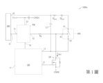
第1圖為一比較例的電源轉換設備的控制裝置1000a的電路圖。如第1圖所示,控制裝置1000a包括米勒開關控制電路100、控制晶片400、驅動電路500及功率模組600。控制晶片400對於驅動電路500進行控制,使得驅動電路500驅動功率模組600執行切換開關的功能。米勒開關控制電路100用於控制功率模組600的米勒箝位電壓。
FIG. 1 is a circuit diagram of a
更具體而言,驅動電路500的高電位端53連接於定電壓V1+。驅動電路500的低電位端54連接於米勒開關控制電路100。驅動電路500的輸入端51連接於控制晶片400的輸出端41,驅動電路500經由輸入端51接受控制晶片400的控制。驅動電路500的輸出端52經由電阻Rg連接於功率模組600的控制端63,驅動電路500經由輸出端52驅動功率模組600。
More specifically, the high
功率模組600作為為功率開關,其具有切換功能。當電源轉換設備提供電力至不同功率規格的設備時,功率模組600因應於不同功率進行該關切換。功率模組600的控制端63接收驅動電路500的驅動電壓,因應於驅動電壓,功率模組600為導通(turned-on)的狀態或斷開(turned-off)的狀態。當功率模組600為導通時,功率模組600的第一端61可導通於第二端62。功率模組600可包括功率半導體元件,在一種示例中,功率模組600的功率半導體元件例如是電晶體(第1圖中未顯示)。電晶體的汲極連接於
第一端61,電晶體的源極連接於第二端62,電晶體的閘極連接於控制端63。
The
功率模組600的控制端63連接於電晶體Q6,且電晶體Q6連接於接地端GND0。即,電晶體Q6設置於功率模組600的控制端63與接地端GND0之間。電晶體Q6作為米勒開關以提供米勒電流Im1的旁路傳輸路徑。電晶體Q6的源極經由電阻Rg連接於驅動電路500的輸出端52,電晶體Q6的汲極連接於接地端GND0。電晶體Q6的閘極連接於米勒開關控制電路100的輸出端12,米勒開關控制電路100的輸入端13連接於電容C3及功率模組600的第二端62。米勒開關控制電路100用於控制電晶體Q6為導通的時間,即,米勒開關控制電路100用於控制米勒開關驅動時間tmiller(亦可稱為「米勒鉗位時間」)。並且,米勒開關控制電路100用於控制功率模組600的電晶體的米勒箝位電壓Vmiller。
The
功率模組600的第一端61經由電阻Rdesat及二極體Ddesat連接至控制晶片400的輸出端42。功率模組600的第二端62經由電容C3連接於電阻Rdesat。當功率模組600發生短路時,電阻Rdesat及二極體Ddesat形成的傳輸路徑可導引功率模組600產生的飽和電流,以達到功率模組600的短路保護之功效。即,電阻Rdesat及二極體Ddesat作為功率模組600的短路保護電路。
The
第2圖為本揭示一實施例的電源轉換設備的控制裝置1000b的電路圖。如第2圖所示,控制裝置1000b包括米勒開關控制電路100、溫度補償保護電路300、控制晶片400、驅動電路500
及功率模組600。即,第2圖的實施例的控制裝置1000b類似於第1圖的比較例的控制裝置1000a,差異在於:第2圖的控制裝置1000b更包括溫度補償保護電路300。
FIG. 2 is a circuit diagram of a
驅動電路500包括電晶體Q1及電晶體Q2。電晶體Q1及電晶體Q2形成反向器(inverter)。電晶體Q1、Q2兩者的閘極共同連接於驅動電路500的輸入端51,電晶體Q1、Q2兩者的汲極共同連接於驅動電路500的輸出端52。驅動電路500的輸入端51連接於米勒開關控制電路100的輸入端11及控制晶片400的輸出端41。驅動電路500的輸出端52經由電阻Rg連接於功率模組600的控制端63。
The driving
電阻Rdesat及二極體Ddesat作為功率模組600的短路保護電路,溫度補償保護電路300可對於電阻Rdesat及二極體Ddesa進行溫度補償。溫度補償保護電路300包括第一端31、第二端32、第三端33及第四端34。其中,溫度補償保護電路300的第一端31經由電阻Rdesat及二極體Ddesat連接於功率模組600的第一端61,且第一端31經由電容C3連接於功率模組600的第二端62。溫度補償保護電路300的第二端32連接於功率模組600的感測端64。溫度補償保護電路300的第三端33連接於控制晶片400的輸入端43。溫度補償保護電路300的第四端34連接於控制晶片400的輸出端42。
The resistor R desat and the diode D desat serve as a short circuit protection circuit of the
在運作上,溫度補償保護電路300經由功率模組600的感測端64感測功率模組600的溫度。因應於功率模組600
的不同溫度,溫度補償保護電路300提供對應的補償電流至電阻Rdesat及二極體Ddesat形成的傳輸路徑,以達到溫度補償的功效。
In operation, the temperature
第3圖為第2圖的控制裝置1000b之中的溫度補償保護電路300的電路圖。請同時參見第2圖及第3圖,溫度補償保護電路300的第三端33連接於控制晶片400的輸入端43,且第三端33連接於第三定電壓V2+。控制晶片400的輸出端42經由電容C22連接於接地端GND2。電阻Rdesat及二極體Ddesat的傳輸路徑可提供功率模組600的短路保護。當功率模組600發生短路時,功率模組600的電晶體Q5可能產生飽和電流,電阻Rdesat及二極體Ddesat可提供電晶體Q5的飽和電流的傳輸路徑。溫度補償保護電路300可因應於功率模組600的溫度變化產生對應的補償電流I1,補償電流I1提供至電阻Rdesat及二極體Ddesat形成的傳輸路徑以達到溫度補償的功效。
FIG. 3 is a circuit diagram of the temperature
溫度補償保護電路300包括感測器310、處理器320、電流源330及二極體D3。功率模組600的第一端61經由電阻Rdesat、二極體Ddesat連接於溫度補償保護電路300的二極體D3,並且經由二極體D3連接於控制晶片400的輸出端42。功率模組600的感測端64連接於感測器310。感測器310例如為溫度感測器,感測器310用於感測功率模組600的溫度temp1。
The temperature
功率模組600的溫度temp1之變化範圍例如為攝氏25度至攝氏175度。操作於攝氏25度至攝氏175度的範圍內,功率模組600的電晶體Q5的汲極-源極電壓Vds5具有不同電壓
值,且電晶體Q5的汲極-源極電流Ids5具有不同電流量。其中,汲極-源極電壓Vds5為電晶體Q5的汲極d5與源極s5之電壓差。
The temperature temp1 of the
在本實施例中,溫度補償保護電路300的預設操作條件為:當功率模組600的溫度temp1大致相等於175度時,溫度補償保護電路300提供的補償電流I1的電流量為零。基於上述的預設操作條件,電阻Rdesat的電阻值R_desat可根據式(1)而得到:

式(1)的「Vref」為控制晶片400的參考電壓Vref。式(1)的「V_D3」為二極體D3的順向偏壓。式(1)的「V_D_desat」為二極體Ddesat的順向偏壓。式(1)的「Vds5(175°)」為溫度temp1大致相等於175度時汲極-源極電壓Vds5的電壓值。式(1)的「I0」為控制晶片400內部的電流源410提供的電流I0的電流量。即,電阻Rdesat的電阻值R_desat係相關於功率模組600的溫度temp1與電晶體Q5的汲極d5與源極s5之電壓差。
"V ref " in formula (1) is the reference voltage V ref of the
感測器310經由溫度補償保護電路300的第二端32連接於功率模組600的感測端64,以感測功率模組600的溫度temp1。因應於功率模組600的溫度temp1,感測器310提供對應的控制訊號至處理器320。並且,處理器320提供對應的控制訊號至電流源330。在本實施例中,電流源330為電壓控制型電流源(簡稱為「壓控電流源」),處理器320產生的控制訊號為電
壓控制訊號,此電壓控制訊號是隨著功率模組600的溫度temp1而改變。電流源330用於產生補償電流I1,補償電流I1的電流量因應於處理器320的電壓控制訊號而改變,如式(2)所示:

式(2)中的「Vds5(temp1)」為電晶體Q5操作於溫度temp1時的汲極-源極電壓Vds5的電壓值。電流源330提供的補償電流I1可作為電阻Rdesat及二極體Ddesat形成的短路保護電路的電流補償。電流源330因應於溫度temp1之變化而改變補償電流I1的電流量以達到溫度補償的功效。並且,溫度補償保護電路300的二極體D3可阻絕電阻Rdesat及二極體Ddesat的傳輸路徑上可能產生的逆向電流。
"Vds5(temp1)" in formula (2) is the voltage value of the drain-source voltage Vds5 of the transistor Q5 when it operates at the temperature temp1. The compensation current I1 provided by the
根據感測器310感測到的功率模組600的溫度temp1,處理器320可根據查表(table lookup)而產生對應的電壓控制訊號,據以控制電流源330產生適當的補償電流I1。據此,當功率模組600的溫度temp1之變化範圍較大時,溫度補償保護電路300仍可精準提供適當的補償電流I1。此外,控制晶片400的比較器420對於輸出端42的電壓值與參考電壓Vref進行比較,比較器420根據比較結果產生指示電壓Vfault。
According to the temperature temp1 of the
第4A圖為本揭示一實施例的電源轉換設備2000的方塊圖。電源轉換設備2000包括電源2100、功率模組620、儲能元件2200、負載2300及控制電路700。控制電路700可包括
第2圖的實施例的米勒開關控制電路100及溫度補償保護電路300(第4A圖中未顯示)。電源2100例如為大型之固定的電網設備。儲能元件2200例如為小型(甚至為可攜式)的電池裝置。功率模組620設置於電源2100與儲能元件2200之間,功率模組620作為切換開關。因應於不同功率規格的電源2100、儲能元件2200及負載2300,功率模組620對於電源2100提供的電力進行轉換,以產生特定功率及特定形式的電力並提供至儲能元件2200。
FIG. 4A is a block diagram of a
控制電路700連接於功率模組620。功率模組620之中的功率半導體元件可能肇因於米勒效應而導致功率模組620的短路或誤動作。對應的,控制電路700對於功率模組620之中的功率半導體元件進行米勒鉗位控制。例如:控制電路700將功率模組620之中的功率半導體元件的閘極-源極電壓控制於適當的米勒箝位電壓Vmiller,且將米勒開關控制於操作在適當的米勒開關驅動時間tmiller。
The
接著,請參見第4B圖,其繪示第4A圖的電源轉換設備2000之一實施例的示意圖。本實施例的功率模組620包括六個功率開關元件,對應的,控制電路700包括六個控制單元710~760。功率模組620的每個功率開關元件具有切換開關的功能,功率模組620的每個功率開關元件由控制電路700的控制單元710~760之對應一者來控制。例如,控制電路700的控制單元710、720分別控制功率模組620的一組功率開關元件,該組功率開關元件作為功率模組620的上臂元件與下臂元件。類似的,控
制電路700的控制單元730、740分別控制功率模組620的另一組功率開關元件,控制電路700的控制單元750、760分別控制功率模組620的又一組功率開關元件。
Next, please refer to FIG. 4B, which is a schematic diagram of an embodiment of the
雖然本發明已以較佳實施例及範例詳細揭示如上,可理解的是,此些範例意指說明而非限制之意義。可預期的是,所屬技術領域中具有通常知識者可想到多種修改及組合,其多種修改及組合落在本發明之精神以及後附之申請專利範圍之範圍內。 Although the present invention has been disclosed in detail above with preferred embodiments and examples, it is understood that these examples are intended to be illustrative rather than restrictive. It is expected that a person with ordinary knowledge in the relevant technical field can think of various modifications and combinations, and the various modifications and combinations fall within the spirit of the present invention and the scope of the attached patent application.
300:溫度補償保護電路 300: Temperature compensation protection circuit
310:感測器 310:Sensor
320:處理器 320: Processor
330:電流源 330: Current source
400:控制晶片 400: Control chip
410:電流源 410: Current source
420:比較器 420: Comparator
600:功率模組 600: Power module
13,43:輸入端 13,43: Input port
42:輸出端 42: Output terminal
31,61:第一端 31,61: First end
32:第二端 32: Second end
33:第三端 33: The third end
34:第四端 34: The fourth end
64:感測端 64: Sensing end
C22,C3:電容 C22,C3: Capacitor
Rdesat:電阻 R desat : resistance
D3,Ddesat:二極體 D3,D desat : diode
I1:補償電流 I1: Compensation current
I0:電流 I0: current
V2+:定電壓 V2+: constant voltage
GND2:接地端 GND2: ground terminal
temp1:溫度 temp1: temperature
Q5:電晶體 Q5: Transistor
d5:汲極 d5: Drain
s5:源極 s5: Source
Vds5:汲極-源極電壓 Vds5: drain-source voltage
Vref:參考電壓 V ref : reference voltage
Vfault:指示電壓 V fault : Indication voltage
Claims (8)
Priority Applications (2)
| Application Number | Priority Date | Filing Date | Title |
|---|---|---|---|
| TW112113863A TWI849842B (en) | 2023-04-13 | 2023-04-13 | Control device applied to power conversion apparatus |
| CN202310509967.1A CN118801688A (en) | 2023-04-13 | 2023-05-08 | Control device for power conversion equipment |
Applications Claiming Priority (1)
| Application Number | Priority Date | Filing Date | Title |
|---|---|---|---|
| TW112113863A TWI849842B (en) | 2023-04-13 | 2023-04-13 | Control device applied to power conversion apparatus |
Publications (2)
| Publication Number | Publication Date |
|---|---|
| TWI849842B true TWI849842B (en) | 2024-07-21 |
| TW202443335A TW202443335A (en) | 2024-11-01 |
Family
ID=92929648
Family Applications (1)
| Application Number | Title | Priority Date | Filing Date |
|---|---|---|---|
| TW112113863A TWI849842B (en) | 2023-04-13 | 2023-04-13 | Control device applied to power conversion apparatus |
Country Status (2)
| Country | Link |
|---|---|
| CN (1) | CN118801688A (en) |
| TW (1) | TWI849842B (en) |
Citations (4)
| Publication number | Priority date | Publication date | Assignee | Title |
|---|---|---|---|---|
| CN103023416A (en) * | 2011-09-22 | 2013-04-03 | 通用汽车环球科技运作有限责任公司 | System and method for current estimation for operation of electric motors |
| TWI657647B (en) * | 2018-06-12 | 2019-04-21 | 大陸商昂寶電子(上海)有限公司 | Short-circuit protection system for current sensing terminal in switching power supply |
| TWM606468U (en) * | 2020-09-09 | 2021-01-11 | 士林電機廠股份有限公司 | Temperature compensation short circuit protecting circuit of power solid-state switch |
| US20220216796A1 (en) * | 2020-03-18 | 2022-07-07 | Shenzhen Huntkey Electric Co., Ltd. | Switching power supply, power adapter and charger |
-
2023
- 2023-04-13 TW TW112113863A patent/TWI849842B/en active
- 2023-05-08 CN CN202310509967.1A patent/CN118801688A/en active Pending
Patent Citations (4)
| Publication number | Priority date | Publication date | Assignee | Title |
|---|---|---|---|---|
| CN103023416A (en) * | 2011-09-22 | 2013-04-03 | 通用汽车环球科技运作有限责任公司 | System and method for current estimation for operation of electric motors |
| TWI657647B (en) * | 2018-06-12 | 2019-04-21 | 大陸商昂寶電子(上海)有限公司 | Short-circuit protection system for current sensing terminal in switching power supply |
| US20220216796A1 (en) * | 2020-03-18 | 2022-07-07 | Shenzhen Huntkey Electric Co., Ltd. | Switching power supply, power adapter and charger |
| TWM606468U (en) * | 2020-09-09 | 2021-01-11 | 士林電機廠股份有限公司 | Temperature compensation short circuit protecting circuit of power solid-state switch |
Also Published As
| Publication number | Publication date |
|---|---|
| TW202443335A (en) | 2024-11-01 |
| CN118801688A (en) | 2024-10-18 |
Similar Documents
| Publication | Publication Date | Title |
|---|---|---|
| TWI441134B (en) | Gate drive circuit and semiconductor device | |
| CN109088532B (en) | A current mode segmented gate drive circuit with active clamp | |
| Yin et al. | A novel gate assisted circuit to reduce switching loss and eliminate shoot-through in SiC half bridge configuration | |
| JP2018182818A (en) | Switching element drive device | |
| CN108682672A (en) | High-power semiconductor module suitable for the soaking under Short-circuit Working Condition of internal power switch chip | |
| CN201656951U (en) | Insulated gate bipolar translator drive circuit | |
| CN212012597U (en) | Overcurrent protection circuit based on integrated gallium nitride power device | |
| JP7132099B2 (en) | power converter | |
| TWI849842B (en) | Control device applied to power conversion apparatus | |
| CN112614826B (en) | Dual-gate power metal oxide semiconductor field effect transistor and its driving circuit | |
| CN112953174B (en) | Clamping active driving circuit for inhibiting SiC MOSFET crosstalk based on dv/dt detection | |
| CN111555596B (en) | A SiC MOSFET gate crosstalk suppression drive circuit with adjustable negative voltage | |
| CN116346099A (en) | Gate driving circuit of cascade type power device and integrated semiconductor power device | |
| JP6706876B2 (en) | Power module | |
| CN118012220A (en) | SiC MOSFET active gate driving circuit based on Wilson current mirror | |
| TWI846201B (en) | Control device for power conversion apparatus | |
| CN114244339B (en) | Gate drive circuit and electronic device | |
| CN106953624B (en) | MOSFET parallel overcurrent protection circuit | |
| CN116449249A (en) | Silicon carbide MOSFET short circuit detection circuit and device | |
| Liu et al. | Review of SiC MOSFET drive circuit | |
| JPH06105448A (en) | Switch device with protecting function | |
| CN222262477U (en) | Driving circuit of power module | |
| CN116614121B (en) | Power device for improving electromagnetic compatibility | |
| Liang et al. | Natural Active Gate Driving for Breaking Trade-off Between Switching Loss and Current Overshoot Using Ordinary Gate Driver | |
| TWI853557B (en) | Drive device |