TWI831333B - Memory controller and method for accessing flash memory - Google Patents
Memory controller and method for accessing flash memory Download PDFInfo
- Publication number
- TWI831333B TWI831333B TW111131088A TW111131088A TWI831333B TW I831333 B TWI831333 B TW I831333B TW 111131088 A TW111131088 A TW 111131088A TW 111131088 A TW111131088 A TW 111131088A TW I831333 B TWI831333 B TW I831333B
- Authority
- TW
- Taiwan
- Prior art keywords
- value
- codeword
- memory
- variable node
- decoding
- Prior art date
Links
- 238000000034 method Methods 0.000 title claims abstract description 68
- 208000011580 syndromic disease Diseases 0.000 claims abstract description 48
- 230000004044 response Effects 0.000 claims abstract description 10
- 208000024891 symptom Diseases 0.000 claims description 46
- 230000008569 process Effects 0.000 claims description 36
- 238000013500 data storage Methods 0.000 claims description 16
- 239000011159 matrix material Substances 0.000 description 37
- 238000010586 diagram Methods 0.000 description 15
- 238000012545 processing Methods 0.000 description 9
- 238000012937 correction Methods 0.000 description 7
- 238000012795 verification Methods 0.000 description 7
- 238000004891 communication Methods 0.000 description 5
- 238000005516 engineering process Methods 0.000 description 4
- 230000005540 biological transmission Effects 0.000 description 3
- 238000004364 calculation method Methods 0.000 description 3
- 230000008859 change Effects 0.000 description 3
- 230000006870 function Effects 0.000 description 3
- 230000003862 health status Effects 0.000 description 2
- 238000007796 conventional method Methods 0.000 description 1
- 230000007717 exclusion Effects 0.000 description 1
- 238000000605 extraction Methods 0.000 description 1
- 230000010354 integration Effects 0.000 description 1
- 230000003993 interaction Effects 0.000 description 1
- 238000012986 modification Methods 0.000 description 1
- 230000004048 modification Effects 0.000 description 1
- 239000013307 optical fiber Substances 0.000 description 1
- 230000002093 peripheral effect Effects 0.000 description 1
- 239000004065 semiconductor Substances 0.000 description 1
- 239000007787 solid Substances 0.000 description 1
- 230000003068 static effect Effects 0.000 description 1
Images


Classifications
-
- H—ELECTRICITY
- H03—ELECTRONIC CIRCUITRY
- H03M—CODING; DECODING; CODE CONVERSION IN GENERAL
- H03M13/00—Coding, decoding or code conversion, for error detection or error correction; Coding theory basic assumptions; Coding bounds; Error probability evaluation methods; Channel models; Simulation or testing of codes
- H03M13/03—Error detection or forward error correction by redundancy in data representation, i.e. code words containing more digits than the source words
- H03M13/05—Error detection or forward error correction by redundancy in data representation, i.e. code words containing more digits than the source words using block codes, i.e. a predetermined number of check bits joined to a predetermined number of information bits
- H03M13/11—Error detection or forward error correction by redundancy in data representation, i.e. code words containing more digits than the source words using block codes, i.e. a predetermined number of check bits joined to a predetermined number of information bits using multiple parity bits
- H03M13/1102—Codes on graphs and decoding on graphs, e.g. low-density parity check [LDPC] codes
- H03M13/1105—Decoding
- H03M13/1128—Judging correct decoding and iterative stopping criteria other than syndrome check and upper limit for decoding iterations
-
- H—ELECTRICITY
- H03—ELECTRONIC CIRCUITRY
- H03M—CODING; DECODING; CODE CONVERSION IN GENERAL
- H03M13/00—Coding, decoding or code conversion, for error detection or error correction; Coding theory basic assumptions; Coding bounds; Error probability evaluation methods; Channel models; Simulation or testing of codes
- H03M13/03—Error detection or forward error correction by redundancy in data representation, i.e. code words containing more digits than the source words
- H03M13/05—Error detection or forward error correction by redundancy in data representation, i.e. code words containing more digits than the source words using block codes, i.e. a predetermined number of check bits joined to a predetermined number of information bits
- H03M13/11—Error detection or forward error correction by redundancy in data representation, i.e. code words containing more digits than the source words using block codes, i.e. a predetermined number of check bits joined to a predetermined number of information bits using multiple parity bits
- H03M13/1102—Codes on graphs and decoding on graphs, e.g. low-density parity check [LDPC] codes
- H03M13/1105—Decoding
- H03M13/1108—Hard decision decoding, e.g. bit flipping, modified or weighted bit flipping
-
- G—PHYSICS
- G06—COMPUTING; CALCULATING OR COUNTING
- G06F—ELECTRIC DIGITAL DATA PROCESSING
- G06F3/00—Input arrangements for transferring data to be processed into a form capable of being handled by the computer; Output arrangements for transferring data from processing unit to output unit, e.g. interface arrangements
- G06F3/06—Digital input from, or digital output to, record carriers, e.g. RAID, emulated record carriers or networked record carriers
- G06F3/0601—Interfaces specially adapted for storage systems
- G06F3/0602—Interfaces specially adapted for storage systems specifically adapted to achieve a particular effect
- G06F3/0625—Power saving in storage systems
-
- G—PHYSICS
- G06—COMPUTING; CALCULATING OR COUNTING
- G06F—ELECTRIC DIGITAL DATA PROCESSING
- G06F3/00—Input arrangements for transferring data to be processed into a form capable of being handled by the computer; Output arrangements for transferring data from processing unit to output unit, e.g. interface arrangements
- G06F3/06—Digital input from, or digital output to, record carriers, e.g. RAID, emulated record carriers or networked record carriers
- G06F3/0601—Interfaces specially adapted for storage systems
- G06F3/0628—Interfaces specially adapted for storage systems making use of a particular technique
- G06F3/0655—Vertical data movement, i.e. input-output transfer; data movement between one or more hosts and one or more storage devices
- G06F3/0656—Data buffering arrangements
-
- G—PHYSICS
- G06—COMPUTING; CALCULATING OR COUNTING
- G06F—ELECTRIC DIGITAL DATA PROCESSING
- G06F3/00—Input arrangements for transferring data to be processed into a form capable of being handled by the computer; Output arrangements for transferring data from processing unit to output unit, e.g. interface arrangements
- G06F3/06—Digital input from, or digital output to, record carriers, e.g. RAID, emulated record carriers or networked record carriers
- G06F3/0601—Interfaces specially adapted for storage systems
- G06F3/0628—Interfaces specially adapted for storage systems making use of a particular technique
- G06F3/0655—Vertical data movement, i.e. input-output transfer; data movement between one or more hosts and one or more storage devices
- G06F3/0658—Controller construction arrangements
-
- G—PHYSICS
- G06—COMPUTING; CALCULATING OR COUNTING
- G06F—ELECTRIC DIGITAL DATA PROCESSING
- G06F3/00—Input arrangements for transferring data to be processed into a form capable of being handled by the computer; Output arrangements for transferring data from processing unit to output unit, e.g. interface arrangements
- G06F3/06—Digital input from, or digital output to, record carriers, e.g. RAID, emulated record carriers or networked record carriers
- G06F3/0601—Interfaces specially adapted for storage systems
- G06F3/0668—Interfaces specially adapted for storage systems adopting a particular infrastructure
- G06F3/0671—In-line storage system
- G06F3/0673—Single storage device
- G06F3/0679—Non-volatile semiconductor memory device, e.g. flash memory, one time programmable memory [OTP]
-
- G—PHYSICS
- G11—INFORMATION STORAGE
- G11C—STATIC STORES
- G11C16/00—Erasable programmable read-only memories
- G11C16/02—Erasable programmable read-only memories electrically programmable
- G11C16/06—Auxiliary circuits, e.g. for writing into memory
- G11C16/08—Address circuits; Decoders; Word-line control circuits
-
- G—PHYSICS
- G11—INFORMATION STORAGE
- G11C—STATIC STORES
- G11C16/00—Erasable programmable read-only memories
- G11C16/02—Erasable programmable read-only memories electrically programmable
- G11C16/06—Auxiliary circuits, e.g. for writing into memory
- G11C16/10—Programming or data input circuits
-
- G—PHYSICS
- G11—INFORMATION STORAGE
- G11C—STATIC STORES
- G11C16/00—Erasable programmable read-only memories
- G11C16/02—Erasable programmable read-only memories electrically programmable
- G11C16/06—Auxiliary circuits, e.g. for writing into memory
- G11C16/26—Sensing or reading circuits; Data output circuits
-
- H—ELECTRICITY
- H03—ELECTRONIC CIRCUITRY
- H03M—CODING; DECODING; CODE CONVERSION IN GENERAL
- H03M13/00—Coding, decoding or code conversion, for error detection or error correction; Coding theory basic assumptions; Coding bounds; Error probability evaluation methods; Channel models; Simulation or testing of codes
- H03M13/03—Error detection or forward error correction by redundancy in data representation, i.e. code words containing more digits than the source words
- H03M13/05—Error detection or forward error correction by redundancy in data representation, i.e. code words containing more digits than the source words using block codes, i.e. a predetermined number of check bits joined to a predetermined number of information bits
- H03M13/11—Error detection or forward error correction by redundancy in data representation, i.e. code words containing more digits than the source words using block codes, i.e. a predetermined number of check bits joined to a predetermined number of information bits using multiple parity bits
- H03M13/1102—Codes on graphs and decoding on graphs, e.g. low-density parity check [LDPC] codes
- H03M13/1105—Decoding
- H03M13/1111—Soft-decision decoding, e.g. by means of message passing or belief propagation algorithms
-
- H—ELECTRICITY
- H03—ELECTRONIC CIRCUITRY
- H03M—CODING; DECODING; CODE CONVERSION IN GENERAL
- H03M13/00—Coding, decoding or code conversion, for error detection or error correction; Coding theory basic assumptions; Coding bounds; Error probability evaluation methods; Channel models; Simulation or testing of codes
- H03M13/03—Error detection or forward error correction by redundancy in data representation, i.e. code words containing more digits than the source words
- H03M13/05—Error detection or forward error correction by redundancy in data representation, i.e. code words containing more digits than the source words using block codes, i.e. a predetermined number of check bits joined to a predetermined number of information bits
- H03M13/13—Linear codes
- H03M13/15—Cyclic codes, i.e. cyclic shifts of codewords produce other codewords, e.g. codes defined by a generator polynomial, Bose-Chaudhuri-Hocquenghem [BCH] codes
- H03M13/151—Cyclic codes, i.e. cyclic shifts of codewords produce other codewords, e.g. codes defined by a generator polynomial, Bose-Chaudhuri-Hocquenghem [BCH] codes using error location or error correction polynomials
- H03M13/1575—Direct decoding, e.g. by a direct determination of the error locator polynomial from syndromes and subsequent analysis or by matrix operations involving syndromes, e.g. for codes with a small minimum Hamming distance
Landscapes
- Engineering & Computer Science (AREA)
- Physics & Mathematics (AREA)
- Theoretical Computer Science (AREA)
- General Physics & Mathematics (AREA)
- Probability & Statistics with Applications (AREA)
- Mathematical Physics (AREA)
- General Engineering & Computer Science (AREA)
- Human Computer Interaction (AREA)
- Algebra (AREA)
- Pure & Applied Mathematics (AREA)
- Error Detection And Correction (AREA)
- Detection And Correction Of Errors (AREA)
- Techniques For Improving Reliability Of Storages (AREA)
Abstract
Description
本發明係有關於資料存取,特別是有關於一種記憶體控制器及快閃記憶體的存取方法。 The present invention relates to data access, and in particular to a memory controller and a flash memory access method.
隨著半導體技術的進步,低密度同位元檢查(low-density parity-check,LDPC)碼在近年來已可用超大型積體(very-large-scale integration,VLSI)電路所實現,且廣泛應用於數位通訊領域(例如包括無線通訊及光纖通訊)以及資料傳輸領域(例如用於資料儲存裝置,如快閃記憶體、固態硬碟)以做為錯誤更正碼(error correction code,ECC)。 With the advancement of semiconductor technology, low-density parity-check (LDPC) codes have been implemented in very-large-scale integration (VLSI) circuits in recent years and are widely used in In the field of digital communication (for example, including wireless communication and optical fiber communication) and the field of data transmission (for example, used in data storage devices, such as flash memory and solid state drives) as error correction code (ECC).
低密度同位元檢查解碼器係使用具有同位元(parity bit)的線性錯誤校正碼來進行解碼,其中同位元會提供用以驗證接收到的碼字(codeword)的同位元方程式給LDPC解碼器。舉例來說,低密度同位元查核碼可為一具有固定長度的二進位碼,其中所有的符元(symbol)相加會等於零。 Low-density parity check decoders use linear error correction codes with parity bits for decoding. The parity bits provide the parity equation used to verify the received codeword to the LDPC decoder. For example, the low-density parity check code may be a fixed-length binary code in which all symbols add up to zero.
在資料的編碼過程中,所有的資料位元會被重複執行並且被傳送至對應的編碼器,其中每個編碼器會產生一同位符元(parity symbol)。碼字係由k個訊息位元(information digit)以及r個檢查位元(check digit)所組成。若碼字總共有n位元,則表示k=n-r。上述碼字可用一同位元檢查矩陣來表示,其中該同位元檢查矩陣具有r列(表示方程式的數量)以及n行(表示位元數),如第1圖所示。這些碼之所以被稱為「低密度」是因為相較於同位元檢查矩陣中位元0的數量而言,位元1的數量相對的少。在解碼過程中,每次的同位元檢查皆可視為一同位元查核碼,並隨後與其他同位元查核碼一起進行交互檢查(cross-check),其中解碼會在檢查節點(check node)進行,而交互檢查會在變數節點(variable node)進行。
During the data encoding process, all data bits are repeatedly executed and sent to the corresponding encoder, where each encoder generates a parity symbol. The codeword is composed of k information digits and r check digits. If the codeword has n bits in total, it means k=n-r. The above codeword can be represented by a parity check matrix, where the parity check matrix has r columns (representing the number of equations) and n rows (representing the number of bits), as shown in Figure 1. These codes are called "low density" because the number of
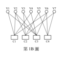
低密度同位元檢查解碼器支持三種模式:硬判定硬解碼(hard decision hard decoding)、軟判定硬解碼(soft decision soft decoding),以及軟判定軟解碼(soft decision hard decoding)。第1A圖係為同位元檢查矩陣H的示意圖。第1B圖係為坦納圖(Tanner Graph)的示意圖。如第1A圖所示,在同位元檢查矩陣H的每一列可形成一檢查節點,例如分別為檢查節點C1、C2、C3及C4。在同位元檢查矩陣H的每一行可形成一變數節點,例如分別為變數節點V1、V2、V3、V4、V5、V6及V7。 The low-density parity check decoder supports three modes: hard decision hard decoding, soft decision soft decoding, and soft decision hard decoding. Figure 1A is a schematic diagram of the parity check matrix H. Figure 1B is a schematic diagram of a Tanner Graph. As shown in FIG. 1A, each column of the parity check matrix H may form a check node, such as check nodes C1, C2, C3 and C4 respectively. Each row of the parity check matrix H may form a variable node, such as variable nodes V1, V2, V3, V4, V5, V6 and V7 respectively.
坦納圖為另一種表示碼字的方式,並且可用於解釋當使用一位元翻轉(bit flipping)演算法時,低密度同位元檢查解碼器的一些關於硬判定軟解碼的操作。 Tanner diagrams are another way of representing codewords and can be used to explain some of the hard-decision soft decoding operations of low-density parity check decoders when using bit flipping algorithms.
如第1B圖所示,在坦納圖中,方形節點C1~C4所表示的檢查節點代表同位元(p arity bit)的數量,且圓形節點V1~V7所表示的變數節點(variable node)係為一碼字中位元的數量。如果一特定方程式與碼符元(code symbol)有關,則對應的檢查節點與變數節點之間會以連線來表示。被估測的資訊會沿著這些連線來傳遞,並且於節點上以不同的方式組合。 As shown in Figure 1B, in the Tanner diagram, the check nodes represented by square nodes C1~C4 represent the number of parity bits, and the variable nodes represented by circular nodes V1~V7 is the number of bits in a codeword. If a specific equation is related to a code symbol, the corresponding check node and variable node will be represented by a connection line. The estimated information is passed along these connections and combined in different ways at the nodes.
當開始進行LDPC解碼時,變數節點將發送一估測資訊(estimate)至所有連線上的檢查節點,其中這些連線包含被認為是正確的位元。接著,每個檢查節點會依據對所有其他的連接的估測(connected estimate)來針對每一變數節點進行新的估測,並且將新的估測資訊傳回至變數節點。新的估測係基於:同位元檢查方程式迫使所有的變數節點連接至一特定檢查節點,以使總和為零。 When LDPC decoding begins, the variable node will send an estimate to the check nodes on all connections that contain bits that are considered correct. Then, each check node will make a new estimate for each variable node based on the estimates of all other connections (connected estimates), and transmit the new estimate information back to the variable node. The new estimate is based on the parity check equation forcing all variable nodes to be connected to a specific check node so that the sum is zero.
這些變數節點會接收新的估測資訊以及使用一多數規則(majority rule)(亦即硬判定),來判斷所傳送的原始位元之數值是否正確。若判斷原始位元之數值不正確,該原始位元會被翻轉(flipped)。該翻轉後的位元接著會被傳回至該些檢查節點,且上述步驟會被疊代地執行一預定次數,直到符合這些檢查節點的同位元檢查方程式。若有符合這些同位元檢查方程式(亦即檢查節點所計算 之數值符合接收自變數節點之數值),則可啟用提前終止(early termination),這會使得系統在最大疊代次數達到之前就結束解碼程序。 These variable nodes will receive new estimation information and use a majority rule (ie, hard decision) to determine whether the value of the original bit transmitted is correct. If the value of the original bit is determined to be incorrect, the original bit will be flipped. The flipped bits are then transmitted back to the check nodes, and the above steps are iteratively performed a predetermined number of times until the parity check equations of the check nodes are met. If there are matching these parity check equations (that is, the check node calculates If the value matches the value of the receiving independent variable node), early termination can be enabled, which will cause the system to end the decoding process before the maximum number of iterations is reached.
該些同位元檢查限制係由進行一徵狀檢查(syndrome check)來實施。一個有效的碼字將會符合方程式:H.CT=S=0,其中H係為同位元檢查矩陣、C係為硬判定碼字(hard decision codeword),且S係為徵狀(syndrome)。當S等於零時,表示解碼程序已完成,且不需要更進一步的資訊。一般來說,硬判定以及徵狀檢查會在疊代期間執行,其中一非零(non-zero)徵狀表示有奇性(odd parity)存在,並且需要再執行新的解碼疊代。 These parity check restrictions are implemented by performing a syndrome check. A valid codeword will conform to the equation: H. C T =S=0, where H is the parity check matrix, C is the hard decision codeword, and S is the syndrome. When S equals zero, it indicates that the decoding process has been completed and no further information is required. Generally, hard decisions and symptom checks are performed during iterations, where a non-zero symptom indicates that odd parity exists and a new decoding iteration needs to be performed.
傳統的位元翻轉LDPC解碼器在解碼階段時,因為碼字資料中的1之數量比例很高,故在記憶體之資料線的切換率(toggle rate)也很高,故傳統的位元翻轉LDPC解碼器之功耗也會相當高。 In the decoding stage of the traditional bit-flip LDPC decoder, because the number of 1s in the codeword data is very high, the switching rate of the data lines in the memory is also very high, so the traditional bit-flip LDPC decoder The power consumption of the LDPC decoder will also be quite high.
因此,本發明係提出一種記憶體控制器及快閃記憶體的存取方法,其可改變在解碼器中在解碼階段之變數節點單元及檢查節點單元的資料控制流程,並可對誤差樣式進行疊代計算,故可讓在變數節點單元中所存取的碼字資料中的1之比例大幅下降,進而大幅降低資料線的切換率並降低解碼器之功耗。本發明之記憶 體控制器除了在解碼階段中可不存取通道值記憶體的通道值,且可進一步依據變數節點記憶體之各項目相應的暫存器數值以決定是否要從變數節點記憶體讀取相應項目的資料、以及依據更新旗標之數值以決定是否將更新碼字中的一或多個碼字位元寫入至變數節點記憶體,故可降低對變數節點記憶體的讀取操作數量及寫入操作數量以進一步降低記憶體控制器之解碼器在進行LDPC解碼時的功耗。 Therefore, the present invention proposes a memory controller and a flash memory access method, which can change the data control flow of the variable node unit and the check node unit in the decoding stage in the decoder, and can perform error patterns. Iterative calculation can greatly reduce the proportion of 1 in the code word data accessed in the variable node unit, thereby greatly reducing the switching rate of the data line and reducing the power consumption of the decoder. Memory of the present invention In addition to not accessing the channel value of the channel value memory during the decoding phase, the bank controller can further decide whether to read the corresponding item from the variable node memory based on the register value corresponding to each item in the variable node memory. data, and determines whether to write one or more codeword bits in the update codeword to the variable node memory based on the value of the update flag, so the number of read operations and writes to the variable node memory can be reduced. The number of operations can further reduce the power consumption of the memory controller's decoder when performing LDPC decoding.
本發明係提供一種記憶體控制器,其中該記憶體控制器所執行的低密度同位元查核(low density parity-check,LDPC)解碼流程係依序包括一初始階段、一解碼階段及一輸出階段,該記憶體控制器包括:一變數節點單元以及一檢查節點單元。在該初始階段,該變數節點單元係執行:從一通道值記憶體取得從一快閃記憶體所讀取的該通道值;將該通道值傳送至該檢查節點單元以計算出一徵狀值;以及因應於該徵狀值不為0,將一變數節點記憶體中之複數個項目之每一者對應的暫存器之數值設定為0,並進入該解碼階段。 The present invention provides a memory controller, wherein the low density parity-check (LDPC) decoding process executed by the memory controller sequentially includes an initial stage, a decoding stage and an output stage. , the memory controller includes: a variable node unit and a check node unit. In the initial stage, the variable node unit executes: obtaining the channel value read from a flash memory from a channel value memory; transmitting the channel value to the check node unit to calculate a syndrome value ; and in response to the symptom value not being 0, setting the value of the register corresponding to each of the plurality of items in a variable node memory to 0, and entering the decoding stage.
在一些實施例中,在該解碼階段,該變數節點單元不從該通道值記憶體取得從該快閃記憶體所讀取的該通道值。 In some embodiments, during the decoding stage, the variable node unit does not obtain the channel value read from the flash memory from the channel value memory.
在一些實施例中,在該解碼階段,於每次LDPC解碼疊代之期間,該變數節點單元係執行:依據該徵狀值以計算一徵狀權重;從變數節點記憶體取得先前碼字中具有該暫存器之數值為1的一或多個第一碼字位元,並將該先前碼字中之其他第二碼字位元 視為0;依據該徵狀權重執行位元翻轉(bit-flipping)演算法以翻動該先前碼字中之該等第一碼字位元及該等第二碼字位元中的一或多個碼字字元以產生一更新碼字;將該更新碼字減去該先前碼字以產生該碼字差值;以及將該碼字差值傳送至該檢查節點單元以更新該徵狀值。 In some embodiments, during the decoding stage, during each LDPC decoding iteration, the variable node unit executes: calculating a symptom weight based on the symptom value; obtaining the previous codeword from the variable node memory. Have one or more first codeword bits with a value of 1 in the register, and replace other second codeword bits in the previous codeword Treated as 0; perform a bit-flipping algorithm according to the syndrome weight to flip one or more of the first codeword bits and the second codeword bits in the previous codeword codeword characters to generate an updated codeword; subtract the previous codeword from the updated codeword to generate the codeword difference; and transmit the codeword difference to the check node unit to update the syndrome value .
在一些實施例中,在將該碼字差值傳送至該檢查節點單元以更新該徵狀值之前,該變數節點單元更將該更新碼字中不為0的一或多個碼字位元相應的更新旗標設定為1、將該更新碼字中具有該更新旗標為1的該一或多個碼字位元寫入該變數節點記憶體、並將寫入至該變數節點記憶體之各碼字位元相應的該暫存器之數值設定為1。 In some embodiments, before transmitting the codeword difference value to the check node unit to update the syndrome value, the variable node unit further sets one or more codeword bits in the updated codeword that are not 0. The corresponding update flag is set to 1, the one or more codeword bits in the update codeword with the update flag set to 1 are written into the variable node memory, and written into the variable node memory The value of the register corresponding to each codeword bit is set to 1.
在一些實施例中,在該解碼階段,因應於該變數節點單元判斷該徵狀值等於0或疊代次數已達到一上限值,該變數節點單元係結束該解碼階段並進入該輸出階段。 In some embodiments, in the decoding phase, in response to the variable node unit determining that the symptom value is equal to 0 or the number of iterations has reached an upper limit, the variable node unit ends the decoding phase and enters the output phase.
在一些實施例中,在該輸出階段,該記憶體控制器係將該變數節點記憶體所儲存的該更新碼字輸出為一變數節點符號值,並將該變數節點符號值設定為一誤差值,其中該記憶體控制器係依據該通道值及該變數節點記憶體之各項目相應的該暫存器之數值以計算解碼結果之各位元。 In some embodiments, during the output stage, the memory controller outputs the updated codeword stored in the variable node memory as a variable node symbol value, and sets the variable node symbol value to an error value. , wherein the memory controller calculates each bit of the decoding result based on the channel value and the value of the register corresponding to each item of the variable node memory.
在一些實施例中,因應於該解碼結果之特定位元在該變數節點記憶體中相應的該暫存器之數值為0,該記憶體控制器 係將該通道值設定為該特定位元。因應於該解碼結果之特定位元在該變數節點記憶體中相應的該暫存器之數值為1,該記憶體控制器係將該特定位元相應的該變數節點符號值與該通道值進行互斥或(XOR)運算以得到該特定位元。 In some embodiments, in response to the value of the register corresponding to the specific bit of the decoding result in the variable node memory being 0, the memory controller Sets the channel value to that specific bit. According to the value of the register corresponding to the specific bit of the decoding result in the variable node memory is 1, the memory controller compares the variable node symbol value corresponding to the specific bit with the channel value. Exclusive OR (XOR) operation to get the specific bit.
本發明更提供一種快閃記憶體的存取方法,應用於一資料儲存裝置中的一記憶體控制器,其中該快閃記憶體的資料讀取過程包括一低密度同位元查核(low-density parity-check,LDPC)解碼過程,且該LDPC解碼過程包括一初始階段、一解碼階段及一輸出階段,該快閃記憶體的存取方法包括:經由一儲存程序將資料儲存至該資料儲存裝置之一快閃記憶體;在該初始階段,該方法包括:從一通道值記憶體取得從該快閃記憶體所讀取的該通道值;依據該通道值以計算出一徵狀值;以及因應於該徵狀值不為0,將一變數節點記憶體中之複數個項目之每一者對應的暫存器之數值設定為0,並進入該解碼階段。 The invention further provides a flash memory access method applied to a memory controller in a data storage device, wherein the data reading process of the flash memory includes a low-density parity check. parity-check (LDPC) decoding process, and the LDPC decoding process includes an initial stage, a decoding stage and an output stage. The access method of the flash memory includes: storing data to the data storage device through a storage program a flash memory; in the initial stage, the method includes: obtaining the channel value read from the flash memory from a channel value memory; calculating a symptom value based on the channel value; and According to the symptom value is not 0, the value of the register corresponding to each of the plurality of items in a variable node memory is set to 0, and the decoding stage is entered.
在一些實施例中,在該解碼階段,該記憶體控制器不從該通道值記憶體取得從該快閃記憶體所讀取的該通道值。 In some embodiments, during the decoding stage, the memory controller does not obtain the channel value read from the flash memory from the channel value memory.
在一些實施例中,在該解碼階段,於每次LDPC解碼疊代之期間,該方法更包括:依據該徵狀值以計算一徵狀權重;從變數節點記憶體取得先前碼字中具有該暫存器之數值為1的一或多個第一碼字位元,並將該先前碼字中之其他第二碼字位元視為0;依據該徵狀權重執行位元翻轉(bit-flipping)演算法以翻動該先前 碼字中之該等第一碼字位元及該等第二碼字位元中的一或多個碼字字元以產生一更新碼字;將該更新碼字減去該先前碼字以產生該碼字差值;以及將該碼字差值傳送至該檢查節點單元以更新該徵狀值。 In some embodiments, during the decoding stage, during each LDPC decoding iteration, the method further includes: calculating a syndrome weight based on the syndrome value; obtaining the previous codeword with the syndrome from the variable node memory. One or more first codeword bits whose value in the register is 1, and other second codeword bits in the previous codeword are regarded as 0; bit flipping (bit- flipping) algorithm to flip the previous The first codeword bits in the codeword and one or more codeword characters in the second codeword bits to generate an updated codeword; subtract the previous codeword from the updated codeword to Generate the codeword difference value; and transmit the codeword difference value to the check node unit to update the symptom value.
在一些實施例中,在將該碼字差值傳送至該檢查節點單元以更新該徵狀值之前,該方法更包括:將該更新碼字中不為0的一或多個碼字位元相應的更新旗標設定為1;將該更新碼字中具有該更新旗標為1的該一或多個碼字位元寫入該變數節點記憶體;以及將寫入至該變數節點記憶體之各碼字位元相應的該暫存器之數值設定為1。 In some embodiments, before transmitting the codeword difference value to the check node unit to update the symptom value, the method further includes: changing one or more codeword bits that are not 0 in the updated codeword. The corresponding update flag is set to 1; writing the one or more codeword bits in the update codeword with the update flag being 1 to the variable node memory; and writing to the variable node memory The value of the register corresponding to each codeword bit is set to 1.
在一些實施例中,在該解碼階段,該方法更包括:因應於該徵狀值等於0或疊代次數已達到一上限值,結束該解碼階段並進入該輸出階段。 In some embodiments, during the decoding phase, the method further includes: in response to the symptom value being equal to 0 or the number of iterations reaching an upper limit, ending the decoding phase and entering the output phase.
在一些實施例中,在該輸出階段,該方法更包括:將該變數節點記憶體所儲存的該更新碼字輸出為一變數節點符號值;將該變數節點符號值設定為一誤差值;以及依據該通道值及該變數節點記憶體之各項目相應的該暫存器之數值以計算解碼結果之各位元。 In some embodiments, during the output stage, the method further includes: outputting the updated codeword stored in the variable node memory as a variable node symbol value; setting the variable node symbol value as an error value; and Each bit of the decoding result is calculated based on the channel value and the value of the register corresponding to each item of the variable node memory.
在一些實施例中,該方法更包括:因應於該解碼結果之特定位元在該變數節點記憶體中相應的該暫存器之數值為0,將該通道值設定為該特定位元;以及因應於該解碼結果之特定位元在該變數節點記憶體中相應的該暫存器之數值為1,將該特定位元 相應的該變數節點符號值與該通道值進行互斥或(XOR)運算以得到該特定位元。 In some embodiments, the method further includes: in response to the value of the register corresponding to the specific bit of the decoding result in the variable node memory being 0, setting the channel value to the specific bit; and According to the value of the register corresponding to the specific bit of the decoding result in the variable node memory is 1, the specific bit is The corresponding variable node symbol value and the channel value perform an exclusive OR (XOR) operation to obtain the specific bit.
200:資料儲存裝置 200:Data storage device
210:記憶體控制器 210:Memory controller
211:處理單元 211: Processing unit
212:儲存單元 212:Storage unit
213:啟動程式 213:Start program
214:編碼器 214:Encoder
215:解碼器 215:Decoder
216:控制邏輯 216:Control logic
218:緩衝記憶體 218: Buffer memory
2181:通道值記憶體 2181: Channel value memory
2182:變數節點記憶體 2182: Variable node memory
2183:暫存器 2183: Temporary register
220:快閃記憶體 220: Flash memory
230:主機 230:Host
240:實體區塊 240:Physical block
241:實體頁面 241:Entity page
250、252:存取介面 250, 252: Access interface
261:亂數編譯器 261: Random number compiler
262:亂數解譯器 262: Random number interpreter
410:變數節點單元 410: Variable node unit
420:檢查節點單元 420: Check node unit
430、530、630:互斥或閘 430, 530, 630: Mutual exclusion or gate
4101:更新旗標 4101: Update flag
S705、S712-S716、S721-S726、S732-S734:步驟 S705, S712-S716, S721-S726, S732-S734: steps
S710:初始階段 S710: Initial stage
S720:解碼階段 S720: decoding stage
S730:輸出階段 S730: Output stage
H:同位元檢查矩陣 H: Homogeneous check matrix
c:列數 c: number of columns
t:行數 t: number of rows
M、K、P:矩陣 M, K, P: matrix
K-1:反矩陣 K -1 : inverse matrix
syndrome:徵狀值 syndrome: symptom value
CH_sgn:通道值 CH_sgn: channel value
Diff:碼字差值; Diff: code word difference;
VN_prev:先前碼字 VN_prev: previous codeword
VN_new:更新碼字 VN_new: update code word
C1-C4:檢查節點 C1-C4: Check nodes
V1-V7:變數節點 V1-V7: variable node
第1A圖係為同位元檢查矩陣的示意圖。 Figure 1A is a schematic diagram of a parity check matrix.
第1B圖係為坦納圖(Tanner Graph)的示意圖。 Figure 1B is a schematic diagram of a Tanner Graph.
第2圖為依據本發明一實施例的資料儲存裝置的方塊圖。 Figure 2 is a block diagram of a data storage device according to an embodiment of the present invention.
第3圖為查核碼檢查矩陣及查核碼產生矩陣的示意圖。 Figure 3 is a schematic diagram of a verification code checking matrix and a verification code generation matrix.
第4圖為依據本發明第一實施例中之解碼器215的方塊圖。
Figure 4 is a block diagram of the
第5圖為依據本發明第二實施例中之解碼器215的方塊圖。
Figure 5 is a block diagram of the
第6圖為依據本發明第三實施例中之解碼器215的方塊圖。
Figure 6 is a block diagram of the
第7A-7C圖為依據本發明一實施例中之快閃記憶體的存取方法的流程圖。 7A-7C are flowcharts of a flash memory access method according to an embodiment of the present invention.
以下說明係為完成發明的較佳實現方式,其目的在於描述本發明的基本精神,但並不用以限定本發明。實際的發明內容必須參考之後的權利要求範圍。 The following description is a preferred implementation manner for completing the invention, and its purpose is to describe the basic spirit of the invention, but is not intended to limit the invention. For the actual invention, reference must be made to the following claims.
必須了解的是,使用於本說明書中的"包含"、"包括"等詞,係用以表示存在特定的技術特徵、數值、方法步驟、作業處 理、元件以及/或組件,但並不排除可加上更多的技術特徵、數值、方法步驟、作業處理、元件、組件,或以上的任意組合。 It must be understood that the words "including" and "including" used in this specification are used to indicate the existence of specific technical characteristics, numerical values, method steps, and operation processes. Processes, components and/or components, but this does not exclude the possibility of adding more technical features, values, method steps, work processes, components, components, or any combination of the above.
於申請專利範圍中使用如"第一"、"第二"、"第三"等詞係用來修飾申請專利範圍中的元件,並非用來表示之間具有優先權順序,先行關係,或者是一個元件先於另一個元件,或者是執行方法步驟時的時間先後順序,僅用來區別具有相同名字的元件。 The use of words such as "first", "second", and "third" in the scope of the patent application are used to modify the elements in the scope of the patent application, and are not used to indicate the order of priority, precedence, or precedence between them. The precedence of one element over another, or the chronological order in which method steps are performed, is only used to distinguish elements with the same name.
第2圖為依據本發明一實施例的資料儲存裝置的方塊圖。 Figure 2 is a block diagram of a data storage device according to an embodiment of the present invention.
在一實施例中,資料儲存裝置200可以是可攜式記憶裝置(例如:符合SD/MMC、CF、MS、XD標準之記憶卡)或是固態硬碟(solid-state drive,SSD),且主機230為一可與資料儲存裝置200連接的電子裝置,例如手機、筆記型電腦、桌上型電腦…等等。在另一實施例中,資料儲存裝置200可以設置在一電子裝置中,例如設置在手機、筆記型電腦、桌上型電腦之中,而此時主裝置130可以是該電子裝置的一處理器。
In one embodiment, the
如第2圖所示,資料儲存裝置200包括一記憶體控制器210及一快閃記憶體220,其中記憶體控制器210係用以存取快閃記憶體220。在一實施例中,記憶體控制器210包括一處理單元211、一儲存單元212、一控制邏輯216、一緩衝記憶體218及存取介面250及252。處理單元211可由專用硬體電路或通用硬體所實現,具有多個處理核心的處理器或是具平行處理能力的多處理器,
且上述實現方式例如可為通用處理器(General-Purpose Processor)、或微控制器(Microcontroller),但本發明並不限於此。
As shown in FIG. 2 , the
儲存單元212可為非揮發性記憶體,例如為唯讀記憶體(read-only memory,ROM)、可擦除式可程式化唯讀記憶體(erasable programmable read-only memory,EPROM)、電子可擦除式可程式化唯讀記憶體(electrically erasable programmable read-only memory,EEPROM)或電子熔絲(E-Fuse)。儲存單元212係儲存啟動程式213,其包括啟動碼(Boot Code)或啟動程式(Bootloader),且可由處理單元211執行,記憶體控制器210基於啟動程式213而完成開機,並開始控制該快閃記憶體220的運作,例如,讀取線上燒錄(In System Programming,ISP)碼。
The
快閃記憶體220例如為NAND快閃記憶體,且快閃記憶體220包括複數個實體區塊(physical block)240,且各實體區塊包括複數個實體頁面(physical page)241。
The
處理單元211與快閃記憶體220間的資料與操作命令傳遞係透過數個電子信號進行協調,上述電子信號包括資料線(data line)、時脈訊號(clock signal)與控制訊號(control signal)。資料線可用以傳遞命令、位址、讀出及寫入的資料;控制訊號線可用以傳遞晶片致能(chip enable,CE)、位址提取致能
(address latch enable,ALE)、命令提取致能(command latch enable,CLE)、寫入致能(write enable,WE)等控制訊號。
The transmission of data and operation commands between the
存取介面250可採用雙倍資料率(double data rate,DDR)通訊協定與快閃記憶體220溝通,例如,開放NAND快閃(open NAND flash interface,ONFI)、雙倍資料率開關(DDR Toggle)或其他介面。處理單元211另可使用存取介面252透過指定通訊協定與主機230進行溝通,例如,通用序列匯流排(universal serial bus,USB)、先進技術附著(advanced technology attachment,ATA)、序列先進技術附著(serial advanced technology attachment,SATA)、快速周邊元件互聯(peripheral component interconnect express,PCI-E)、非揮發性記憶體的傳輸規範(Non-Volatile Memory Express,NVMe)或其他介面。
The
緩衝記憶體218可為一揮發性記憶體,例如包括一動態隨機存取記憶體(dynamic random access memory,DRAM)及/或一靜態隨機存取記憶體(static random access memory,SRAM)。在此實施例,緩衝記憶體218包括一通道值記憶體(channel value memory,CHVMem)2181及變數節點記憶體(variable node memory,VNMem)2182。通道值記憶體2181係用以暫存來自存取介面250所讀取的快閃記憶體220的原始頁面資料(或稱為碼字)、或是用以暫存來自主機230的主機指令。變數節點記憶體2182係用以暫存在進行低密度同位元檢查之解碼過程中
在各變數節點之變數節點資料。此外,通道值記憶體2181所儲存的碼字例如可為硬判定或軟判定之方式由快閃記憶體220所讀取的資訊,其中硬判定(hard decision)是採用單一讀取電壓閾值,故所得到的碼字只有符號(sign)資訊。軟判定(soft decision)則是利用多個讀取電壓閾值,故所得到的碼字除了符號資訊之外,還帶有可靠度資訊,例如每個碼字位元可使用至少一位元的可靠度資訊來表示。若可靠度資訊用一位元表示,則可用0及1分別表示強(strong)及弱(weak)兩種不同的可靠度,則碼字位元搭配可靠度則可分為強”1”、弱”1”、弱”0”及強”0”。
The
控制邏輯216包括一編碼器214、一解碼器215、一亂數編譯器(randomizer)261、及一亂數解譯器(de-randomizer)262。在一些實施例中,編碼器214、解碼器215亂數編譯器261、亂數解譯器262及控制邏輯216例如可為硬體電路,且可由應用導向積體電路(application-specific integrated circuit,ASIC)、現場可程式化邏輯閘陣列(field-programmable gate array,FPGA)、複雜可程式化邏輯裝置(complex programmable logic device,CPLD)、或具有相同功能的邏輯電路所實現,但本發明並不限於此。
The
在一實施例中,亂數編譯器261在編碼流程中例如可設置於編碼器214之前(靠近主機端),意即來自主機230的資料會先經過亂數編譯器261以產生亂數資料,其中在亂數資料中的位元0及
位元1的比例約為50%:50%,意即為0跟1實質上(substantially)各半的亂數資料,藉以增進快閃記憶體220之磨損平衡(wear leveling)。編碼器214例如為一低密度同位元查核碼(LDPC)編碼器,且可以根據來自亂數編譯器261的亂數資料來產生對應的查核碼,且所產生的查核碼符合一查核碼檢查矩陣。具體來說,參考第3圖,假設該查核碼檢查矩陣為一大小為c*t的矩陣(例如,列數c=5,行數t=48),而該查核碼檢查矩陣可以分為左側的矩陣M(大小為c*(t-c))以及右側的矩陣K(大小為c*c),為了找出與該查核碼檢查矩陣所對應的查核碼產生矩陣,可以先找出矩陣K的反矩陣K-1(inverse matrix),之後再將反矩陣(K-1)與矩陣M相乘以得到矩陣P,而矩陣P的轉置矩陣(transpose matrix)便可以作為查核碼產生矩陣。換句話說,在找到矩陣P的轉置矩陣之後,編碼器214可以將來自亂數編譯器261的亂數資料乘以矩陣P的轉置矩陣來得到對應於該些資料的查核碼,而編碼器214之後再將資料與查核碼一起乘上該查核碼檢查矩陣以判斷查核碼是否正確。舉例來說,若是相乘結果等於“0”則判斷編碼正確;而若是相乘結果不等於“0”則判斷編碼錯誤。在判斷編碼正確之後,編碼器214係將亂數資料與對應的查核碼寫入至快閃記憶體220的其中一個實體頁面中。
In one embodiment, the
在此實施例中,解碼器215及亂數解譯器262在解碼流程中之順序係相對於在編碼流程中亂數編譯器261及編碼器214
的順序,意即從快閃記憶體220讀取出來的通道值會先經過解碼器215後再經過亂數解譯器262。在一些實施例中,亂數編譯器261及亂數解譯器262亦可分別稱為擾亂器(scrambler)及解擾器(descrambler)。
In this embodiment, the order of the
解碼器215例如為低密度同位元查核碼(LDPC)解碼器。當主機230發送一讀取指令至資料儲存裝置230,記憶體控制器210係由快閃記憶體220取得儲存的原始頁面資料,例如又稱為通道值。在此實施例中,因為從快閃記憶體220所讀取的通道值尚未經過亂數解譯器262進行亂數解譯,表示通道值中的位元1及位元0的數量也是實質上各佔50%。通道值例如包括初始亂數資料及錯誤校正碼資料。因為初始亂數資料及錯誤校正碼資料在經過通道傳輸時可能產生錯誤,故解碼器215可利用錯誤校正碼資料以對初始亂數資料及/或錯誤校正碼資料本身進行錯誤校正,例如可採用一位元翻轉(bit flipping)演算法進行LDPC解碼。因此,解碼器215所產生的解碼結果即為在編碼器214所輸入的正確亂數資料,亂數資料再經過亂數解譯器262進行亂數解譯以得到原本的頁面資料。
The
在另一實施例中,在編碼流程中之編碼器214及亂數編譯器261、以及在解碼流程中之解碼器215及亂數解譯器262之設置方式與上述實施例略有不同。舉例來說,亂數編譯器215及亂數解譯器262可設置於快閃記憶體端。在編碼流程中,來自主機230的資料會先經過編碼器214進行編碼以產生對應的查核碼,且資料
及對應的查核碼會經過亂數編譯器261以產生亂數資料並寫入快閃記憶體220。在解碼流程中,由快閃記憶體220所讀取的通道值會先經過亂數解譯器262進行亂數解譯以還原為原始資料及對應的查核碼。接著,解碼器215再對亂數解譯器262所產生的原始資料及對應的查核碼進行LDPC解碼,並輸出校正後的正確資料。
In another embodiment, the arrangement of the
需注意的是,無論亂數編譯器261及亂數解譯器262是設置於主機端或快閃記憶體端,本發明之快閃記憶體的存取方法方法均可實施。
It should be noted that no matter whether the
第4圖為依據本發明第一實施例中之解碼器215的方塊圖。如第4圖所示,解碼器215包括一變數節點單元(variable node unit,VNU)410及一檢查節點單元(check node unit,CNU)420。解碼器215中之資料流程例如可分為三個階段:初始階段(initial phase)、解碼階段(decoding phase)及輸出階段(output phase)。
Figure 4 is a block diagram of the
在第一實施例中,在初始階段,解碼器215開始進行LDPC解碼,且變數節點單元410會將變數節點記憶體2182中所暫存的先前碼字重置為0。初始階段即為第一次疊代運算,變數節點單元410會由通道值記憶體2181取得通道值CH_sgn,並將通道值CH_sgn直接旁路傳送(bypass)至檢查節點單元420。其中,上述通道值例如可為使用硬決定(hard decision)或軟決定(soft decision)的方式從快閃記憶體220所讀取的原始頁面資料。
In the first embodiment, in the initial stage, the
檢查節點單元420係依據初始的通道值計算出第一次疊代運算的徵狀值(syndrome),意即可先計算如第1A圖所示的水平列的檢查節點C1~C4。檢查節點單元420並將所計算出的徵狀值傳送至變數節點單元410。變數節點單元410係可依據來自檢查節點單元420的徵狀值以判斷是否需要繼續進行後續變數節點的運算。若徵狀值為0,變數節點單元410係判斷不需要繼續進行後續變數節點的運算,並結束初始階段,並進入輸出階段。若徵狀值不為0,變數節點單元410並依據通道值CH_sgn及來自檢查節點單元420的徵狀值syndrome以計算出徵狀權重(syndrome weight),並依據徵狀權重執行一位元翻轉演算法以決定通道值CH_sgn中一或多個碼字位元需要進行位元翻轉,其中上述位元翻轉演算法可利用本發明領域中之習知技術所實現,故其細節於此不再詳述。
The
接著,變數節點單元410將通道值進行位元翻轉後產生的更新碼字VN_new儲存至變數節點記憶體2182以供後續的疊代運算使用。此時,LDPC解碼的初始階段結束,並進入解碼階段。
Then, the
在解碼階段中,解碼器215中的變數節點單元410及檢查節點單元420會持續進行疊代(iteration),直到檢查節點單元420所產生的徵狀值為止或是已達到疊代次數的上限值為止。舉例來說,在每次疊代運算的期間,變數節點單元410均會先由通道值記憶體2181及變數節點記憶體2182分別取得通道值CH_sgn及先前碼字VN_prev,其中先前碼字VN_prev即為前次疊代運算中所產
生並儲存至變數節點記憶體2182的更新碼字VN_new。變數節點單元410並依據通道值CH_sgn及來自檢查節點單元420的徵狀值syndrome以計算出一徵狀權重(syndrome weight),並依據徵狀權重執行上述位元翻轉演算法以決定通道值CH_sgn中一或多個碼字位元需要進行位元翻轉。接著,變數節點單元410將通道值進行位元翻轉後產生的更新碼字VN_new儲存至變數節點記憶體2182以供後續的疊代運算使用。變數節點單元410並計算上述更新碼字VN_new與先前碼字VN_prev之間的差值Diff,並將差值Diff傳送至檢查節點單元420以進行徵狀(syndrome)值的相關運算。當在解碼階段中之一特定疊代運算所產生的徵狀值為0或是疊代次數已達到一上限值,則解碼階段結束,並進入輸出階段。
In the decoding phase, the
在輸出階段中,解碼器215可將儲存於變數節點單元410中的更新碼字VN_new輸出以做為解碼結果。此外,更新碼字VN_new及通道值會經過一互斥或閘430以得到解碼結果及通道值之間的誤差值,其中利用上述誤差值可得知通道值中有幾個位元產生錯誤,故可用於判斷快閃記憶體220目前的健康狀況(health status)。
In the output stage, the
第5圖為依據本發明第二實施例中之解碼器215的方塊圖。在第二實施例中,在第5圖中之變數節點單元410及檢查節點單元420之電路功能與第4圖相同,但第5圖之資料控制流程與第4圖不同。
Figure 5 is a block diagram of the
舉例來說,在初始階段,解碼器215開始進行LDPC解碼,且變數節點單元410會將變數節點記憶體2182中所暫存的先前碼字重置為0。初始階段即為第一次疊代運算,變數節點單元410同樣會由通道值記憶體2181取得通道值CH_sgn,並將通道值CH_sgn直接旁路傳送(bypass)至檢查節點單元420。
For example, in the initial stage, the
檢查節點單元420係依據初始的通道值計算出第一次疊代運算的徵狀值(syndrome),並將所計算出的徵狀值傳送至變數節點單元410。變數節點單元410係可依據來自檢查節點單元420的徵狀值以判斷是否需要繼續進行後續變數節點的運算。若徵狀值為0,變數節點單元410係判斷不需要繼續進行後續變數節點的運算,並結束初始階段,並進入輸出階段。若徵狀值不為0,則變數節點單元410則直接將更新碼字VN_new設定為0並將更新碼字VN_new寫入變數節點記憶體2182,並結束初始階段,並進入解碼階段。
The
在解碼階段中,解碼器215中的變數節點單元410及檢查節點單元420會持續進行疊代(iteration),直到檢查節點單元420所產生的徵狀值為止或是已達到疊代次數的上限值為止。然而,第5圖之實施例與第4圖實施例不同之處,在於解碼階段的每次疊代運算的期間,變數節點單元410係由變數節點記憶體2182取得先前碼字VN_prev,但並不從通道值記憶體2181取得通道值CH_sgn。故在解碼階段中,可關閉通道值記憶體2181以節省功耗。
In the decoding phase, the
變數節點單元410並依據來自檢查節點單元420的徵狀值syndrome以計算出一徵狀權重(syndrome weight),並依據徵狀權重執行上述位元翻轉演算法以決定在先前碼字VN_prev中一或多個碼字位元需要進行位元翻轉。接著,變數節點單元410將通道值進行位元翻轉後產生的更新碼字VN_new儲存至變數節點記憶體2182以供後續的疊代運算使用。變數節點單元410並計算上述更新碼字VN_new與先前碼字VN_prev之間的差值Diff,並將差值Diff傳送至檢查節點單元420以進行徵狀(syndrome)值的相關運算。當在解碼階段中之一特定疊代運算所產生的徵狀值為0或是疊代次數已達到一上限值,則解碼階段結束,並進入輸出階段。
The
在輸出階段,解碼器215係將儲存於變數節點記憶體2182中的更新碼字VN_new輸出為變數節點符號值VN_sgn,並將變數節點符號值VN_sgn與通道值CH_sgn經過互斥或閘430以得到解碼結果。因為變數節點記憶體2182所儲存的更新碼字VN_new即為雜訊e經過疊代運算後得到的結果,故可將變數節點記憶體2182所輸出的變數節點符號值VN_sgn做為誤差值,其中利用上述誤差值可得知通道值中有幾個位元產生錯誤,故可用於判斷快閃記憶體220目前的健康狀況(health status)。
In the output stage, the
詳細而言,在第5圖之實施例中的解碼階段,變數節點單元410例如僅對碼字差值進行相關運算,但最後仍然可得到與
第4圖之解碼流程相同的解碼結果。上述現象例如可從LDPC演算法的數學式進行推導。
Specifically, in the decoding stage in the embodiment of FIG. 5, the
舉例來說,因為LDPC演算法為一線性分組碼(linear block code),故兩個不同碼字相加的結果可得到另一個碼字。因此,從快閃記憶體220所讀取而得的通道值y可視為正確碼字c及雜訊e相加的結果,例如可用式(1)表示:y=c ♁ e (1)
For example, because the LDPC algorithm is a linear block code, the result of adding two different codewords can be another codeword. Therefore, the channel value y read from the
同位元檢查矩陣H與通道值y之內積可得到徵狀值S,例如可用式(2)表示:H.y T =S T (2) The symptom value S can be obtained by the inner product of the same bit check matrix H and the channel value y, which can be expressed by equation (2): H. y T = S T (2)
將式(1)代入式(2),可得到式(3):H.(c T ♁ e T )=S T (3) Substituting formula (1) into formula (2), we can get formula (3): H. ( c T ♁ e T )= S T (3)
將式(3)展開後可得到式(4):H.c T +H.e T =S T (4) After expanding formula (3), formula (4) can be obtained: H. c T +H. e T = S T (4)
若將正確碼字c設定為0,則同位元檢查矩陣H與正確碼字c之內積的結果必然為0,故式(4)可改寫為式(5):H.e T =S T (5) If the correct codeword c is set to 0, the result of the inner product of the parity check matrix H and the correct codeword c must be 0, so equation (4) can be rewritten as equation (5): H. e T = S T (5)
意即,在正確碼字c設定為0的情況下,每次LDPC解碼疊代所得到的徵狀值S僅與雜訊e有關,其中雜訊e即可視為錯誤碼字位元。 That is to say, when the correct codeword c is set to 0, the syndrome value S obtained in each LDPC decoding iteration is only related to the noise e, where the noise e can be regarded as an erroneous codeword bit.
將式(4)中的正確碼字c設定為0例如可對應至第5圖實施例中之初始階段,變數節點單元410則直接將更新碼字VN_new設定為0並將更新碼字VN_new寫入變數節點記憶體2182。需注意的是,因為寫入快閃記憶體220之資料是先經過亂數編譯器261產生的亂數資料再經過編碼器214編碼,故在解碼過程式,解碼器215所取得的碼字同樣可視為0與1實質上各佔50%的高密度/高權重的資料。
Setting the correct codeword c in equation (4) to 0, for example, can correspond to the initial stage in the embodiment of FIG. 5. The
在第4圖之實施例中的解碼階段,變數節點記憶體2182所存取的內容即為0與1實質上各佔50%的碼字,故在變數節點記憶體2182之資料線(data line)上的切換率(toggle rate)也相當高,例如可視為50%。
In the decoding stage in the embodiment of Figure 4, the content accessed by the
當使用第5圖實施例中之資料控制流程時,變數節點記憶體2182所存取的內容為誤差樣式(error pattern)。因為正常的快閃記憶體220之原始位元錯誤率(raw bit error rate,RBER)約小於1%,故上述誤差樣式中的”1”之比例約同樣小於1%。因此,變數節點記憶體2182可由第4圖實施例中的50%切換率大幅降低為1%以下,故可大幅節省進行解碼器214的功耗。此外,在第5圖實
施例中的解碼階段並不用存取通道值記憶體2181,故通道值記憶體2181之資料線的切換率為0,可進一步降低解碼器214的功耗。
When using the data control flow in the embodiment of FIG. 5, the content accessed by the
式(5)的運算過程例如可對應至第5圖實施例中之解碼階段,意即在每次LDPC的疊代中均是對雜訊e進行運算,且當解碼階段結束時,儲存於變數節點記憶體2182中的碼字結果(例如稱為變數節點符號值VN_sgn)即為誤差值,且將變數節點符號值VN_sgn與通道值CH_sgn經過互斥或閘532即可得到解碼結果。 The operation process of equation (5) can, for example, correspond to the decoding stage in the embodiment of Figure 5, which means that the noise e is calculated in each iteration of LDPC, and when the decoding stage ends, it is stored in the variable The codeword result in the node memory 2182 (for example, called the variable node symbol value VN_sgn) is the error value, and the decoding result can be obtained by passing the variable node symbol value VN_sgn and the channel value CH_sgn through the mutually exclusive OR gate 532.
第6圖為依據本發明第三實施例中之解碼器215的方塊圖。在第三實施例中,在第6圖中之變數節點單元610及檢查節點單元620之電路功能與第5圖相同,但第6圖之資料控制流程與第5圖略有不同。
Figure 6 is a block diagram of the
舉例來說,在第6圖中的變數節點記憶體2182包括複數個暫存器2183(例如稱為暫存器VNMem_vld),用以記錄在變數節點記憶體2182中之各項目(entry)的有效性。當在變數節點記憶體2182中之特定項目所對應的暫存器之數值=0,表示該特定項目的資料是無效的,且變數節點單元410在該特定項目的後續運算均以0進行處理。在初始階段中,變數節點單元410並不寫入資料至變數節點記憶體2182,而是將各個暫存器2183之數值均設定為0,意即變數節點單元410已在初始階段先將變數節點記憶體2182中之各項目的資料視為無效資料或未更動的資料。因此,在初始階段中,
可以省略變數節點記憶體2182的資料存取操作,故可進一步節省記憶體控制器210的功耗。
For example, the
在解碼階段中,變數節點單元410會判斷在變數節點記憶體2182中之各個暫存器2183的數值,並從變數節點記憶體2182讀取暫存器數值=1所相應之項目的資料。舉例來說,若在變數節點記憶體2182中之特定項目相應的暫存器2183的數值為1,表示該特定項目所儲存的資料為有效資料,且變數節點單元410在解碼過程中會從變數節點記憶體2182讀取該特定項目之資料以進行疊代運算。若在變數節點記憶體2182中之特定項目相應的暫存器2183的數值為0,則變數節點單元410在解碼過程中不會從變數節點記憶體2182讀取該特定項目之資料,而是將該特定項目對應的資料直接視為0。
In the decoding stage, the
接著,變數節點單元410依據徵狀值以計算徵狀權重,並依據徵狀權重以執行位元翻轉演算法以翻轉先前碼字中之一或多個碼字位元以產生更新碼字。變數節點單元410中所設置的複數個更新旗標4101則是對應在更新碼字的各位元的匯流排,且變數節點單元410會依據更新碼字之結果以設定更新碼字之各位元相應的更新旗標4101。舉例來說,若更新碼字中的特定位元不為0(意即等於1),則變數節點單元410會將該特定位元相應的更新旗標設定為1,並將在更新碼字中更新旗標為1的一或多個碼字位元寫入至變
數節點記憶體2182,再將寫入至變數節點記憶體2182之各碼字位元相應的暫存器2183之數值設定為1。
Next, the
詳細而言,變數節點單元410係依據各個暫存器2183之數值以決定是否要從變數節點記憶體2183讀取相應項目的資料。若變數節點記憶體2182中之特定項目相應的暫存器數值為0,則變數節點單元410在解碼階段中並不會從變數節點記憶體2182讀取該特定項目之資料,而是將該特定項目的資料視為0以進行後續疊代運算,故可降低對變數節點記憶體2182的讀取操作數量以降低功耗。
Specifically, the
此外,變數節點單元410在解碼階段中亦不會將整個更新碼字寫入至變數節點記憶體2182,而是依據各個更新旗標4101之數值以將更新碼字中的一或多個碼字位元寫入至變數節點記憶體2182,故可降低對變數節點記憶體2182的寫入操作數量以降低功耗。
In addition, the
當上述一或多個碼字位元寫入至變數節點記憶體2182後,表示該一或多個碼字位元所在的項目所儲存之資料為有效資料,故變數節點單元410將該一或多個碼字位元所在的項目相應的暫存器2183之數值設定為1。因此,變數節點單元410在下一次疊代運算時,則可從變數節點記憶體2182讀取暫存器數值為1的項目之有效資料。
When the one or more codeword bits are written to the
在輸出階段中,變數節點記憶體2182所儲存的更新碼字即可輸出為變數節點符號值VN_sgn,且解碼器215可將變數節點符號值VN_sgn設定為誤差值。此外,關於LDPC之解碼結果的各位元則需視各暫存器2183之數值以進行按位運算(bitwise operation)。舉例來說,當解碼結果中之特定位元相應的暫存器2183的數值為1,解碼器215將變數節點符號值VN_sgn與通道值CH_sgn進行互斥或(XOR)運算以得到該特定位元。當解碼結果中之特定位元相應的暫存器2183的數值為0,解碼器215將通道值CH_sgn設定為該特定位元。換句話說,解碼結果的各位元前面均設置一多工器,其選擇信號即為解碼結果的各位元相應的暫存器2183之數值(例如VNMem_vld)。若解碼結果有n個位元,則上述選擇操作可用式(6)表示:

for n=0,1,2,....,n-1 for n=0 , 1 , 2 , .... , n-1
第7A-7C圖為依據本發明一實施例中快閃記憶體的存取方法的流程圖。請同時參考第2、6、7A-7C圖,快閃記憶體的資料讀取過程包括LDPC解碼過程,且LDPC解碼過程包括初始階段S710、解碼階段S720及輸出階段S730。在步驟S705,經由一儲存程序將資料儲存至資料儲存裝置200之快閃記憶體220。舉例來說,上述儲存程序例如可將主機欲儲存至資料儲存裝置200的資料
經過編碼流程(例如為LDPC編碼),並將編碼後的資料寫入至快閃記憶體220。
Figures 7A-7C are flowcharts of a flash memory access method according to an embodiment of the present invention. Please refer to Figures 2, 6, and 7A-7C at the same time. The data reading process of the flash memory includes the LDPC decoding process, and the LDPC decoding process includes the initial stage S710, the decoding stage S720, and the output stage S730. In step S705, the data is stored in the
初始階段S710:Initial stage S710:
在步驟S712,變數節點單元410從通道值記憶體2181取得從快閃記憶體220所讀取的一通道值,並將通道值傳送至檢查節點單元420以計算出徵狀值。因為是在LDPC解碼過程中的第一次疊代運算,故變數節點單元410需先將通道值旁通傳送至檢查節點單元420以計算徵狀值。
In step S712, the
在步驟S714,變數節點單元410判斷徵狀值是否等於0?若徵狀值等於0,則直接進入輸出階段S730中的步驟S732。若徵狀值不等於0,則執行步驟S716。舉例來說,徵狀值等於0表示通道值沒有錯誤,故可直接結束初始階段S710,並進入輸出階段S730。徵狀值不等於0表示通道值有錯誤,故需進行後續的解碼階段S720。
In step S714, the
在步驟S716,變數節點單元將更新碼字設定為0並寫入至變數節點記憶體2182。將更新碼字設定為0之用義可參考前述實施例中關於式(4)及式(5)的說明。
In step S716, the variable node unit sets the updated codeword to 0 and writes it into the
解碼階段S720:Decoding stage S720:
在步驟S721,變數節點單元410依據徵狀值計算徵狀權重(syndrome weight)。
In step S721, the
在步驟S722,變數節點單元410由變數節點記憶體2182取得先前碼字中具有暫存器數值為1的一或多個有效碼字位元,並將該先前碼字中之其他碼字位元視為0。舉例來說,變數節點單元410係依據各個暫存器2183之數值以決定是否要從變數節點記憶體2182讀取相應項目的資料。若變數節點記憶體2182中之特定項目相應的暫存器數值為0,則變數節點單元410在解碼階段中並不會從變數節點記憶體2182讀取該特定項目之資料,而是將該特定項目的資料視為0以進行後續疊代運算,故可降低對變數節點記憶體2182的讀取操作數量以降低功耗。因為在初始階段中已將一開始的更新碼字設定0,故在此步驟中的先前碼字可視為誤差碼字,且是針對誤差樣式進行疊代運算。需注意的是,在此步驟中,變數節點單元410並不需再從通道值記憶體2181讀取通道值。
In step S722, the
在步驟S723,變數節點單元410依據徵狀權重執行位元翻轉演算法以翻轉先前碼字中之一或多個碼字位元以產生更新碼字。
In step S723, the
在步驟S724,變數節點單元410將更新碼字中不為0的位元相應的更新旗標設定為1,將更新碼字中更新旗標為1的一或多個碼字位元寫入變數節點記憶體2182,並將寫入至變數節點記憶體之各碼字位元相應的暫存器數值設定為1。舉例來說,變數節點單元410在解碼階段中不會將整個更新碼字寫入至變數節點記憶體2182,而是依據各個更新旗標4101之數值以將更新碼字中的一或
多個碼字位元寫入至變數節點記憶體2182,故可降低對變數節點記憶體2182的寫入操作數量以降低功耗。當上述一或多個碼字位元寫入至變數節點記憶體2182後,表示該一或多個碼字位元所在的項目所儲存之資料為有效資料,故變數節點單元410將該一或多個碼字位元所在的項目相應的暫存器2183之數值設定為1。因此,變數節點單元410在下一次疊代運算時,則可從變數節點記憶體2182讀取暫存器數值為1的項目之有效資料。
In step S724, the
在步驟S725,變數節點單元410將更新碼字及先前碼字之差值Diff傳送至檢查節點單元以計算出徵狀值。類似地,此步驟中的更新碼字同樣可視為更新的誤差碼字,且是針對誤差樣式進行疊代運算。
In step S725, the
在步驟S726,變數節點單元410判斷徵狀值是否等於0。若徵狀值等於0,則結束解碼階段S720並進入輸出階段S730的步驟S732。若徵狀值不等於0,表示仍然需要繼續進行疊代運算,故需回到步驟S721。此外,變數節點單元410於此步驟可再判斷是否已達到疊代次數的上限值。若是,則同樣結束解碼階段S720並進入輸出階段S730的步驟S732。若否且徵狀值不等於0,則回到步驟S721。
In step S726, the
輸出階段S730:Output stage S730:
在步驟S732,解碼器215將變數節點記憶體2182所儲存的更新碼字輸出為變數節點符號值VN_sgn,並將變數節點符號值VN_sgn設定為誤差值。
In step S732, the
在步驟S734,解碼器215依據通道值CH_sgn及變數節點記憶體2182之各項目相應的暫存器數值以計算解碼結果之各位元。舉例來說,關於LDPC之解碼結果的各位元則需視各暫存器2183之數值以進行按位運算(bitwise operation)。當解碼結果中之特定位元相應的暫存器2183的數值為1,解碼器215將該特定位元相應的變數節點符號值VN_sgn與通道值CH_sgn進行互斥或(XOR)運算以得到該特定位元。當解碼結果中之特定位元相應的暫存器2183的數值為0,解碼器215將通道值CH_sgn設定為該特定位元。換句話說,解碼結果的各位元前面均設置一多工器,其選擇信號即為解碼結果的各位元相應的暫存器2183之數值(例如VNMem_vld),其中上述選擇操作可參考式(6)。
In step S734, the
綜上所述,本發明係提出一種記憶體控制器及快閃記憶體的存取方法,其可改變在解碼器中在解碼階段之變數節點單元及檢查節點單元的資料控制流程,並可對誤差樣式進行疊代計算,故可讓在變數節點單元中所存取的碼字資料中的1之比例大幅下降,進而大幅降低資料線的切換率並降低解碼器之功耗。本發明之記憶體控制器除了在解碼階段中可不存取通道值記憶體的通道值,且可進一步依據變數節點記憶體之各項目相應的暫存器數值以 決定是否要從變數節點記憶體讀取相應項目的資料、以及依據更新旗標之數值以決定是否將更新碼字中的一或多個碼字位元寫入至變數節點記憶體,故可降低對變數節點記憶體的讀取操作數量及寫入操作數量以進一步降低記憶體控制器之解碼器在進行LDPC解碼時的功耗。 To sum up, the present invention proposes a memory controller and a flash memory access method, which can change the data control process of the variable node unit and the check node unit in the decoding stage in the decoder, and can also The error pattern is calculated iteratively, so the proportion of 1 in the codeword data accessed in the variable node unit can be greatly reduced, thereby significantly reducing the switching rate of the data line and reducing the power consumption of the decoder. In addition to not accessing the channel values of the channel value memory during the decoding phase, the memory controller of the present invention can further adjust the memory controller according to the corresponding register values of each item in the variable node memory. Decide whether to read the data of the corresponding item from the variable node memory, and decide whether to write one or more codeword bits in the update codeword to the variable node memory based on the value of the update flag, so it can reduce The number of read operations and the number of write operations on the variable node memory can further reduce the power consumption of the memory controller's decoder when performing LDPC decoding.
本發明雖以較佳實施例揭露如上,然其並非用以限定本發明的範圍,任何所屬技術領域中具有通常知識者,在不脫離本發明之精神和範圍內,當可做些許的更動與潤飾,因此本發明之保護範圍當視後附之申請專利範圍所界定者為準。 Although the present invention is disclosed above in terms of preferred embodiments, they are not intended to limit the scope of the present invention. Anyone with ordinary skill in the art may make slight changes and modifications without departing from the spirit and scope of the present invention. Therefore, the scope of protection of the present invention shall be determined by the appended patent application scope.
200:資料儲存裝置 200:Data storage device
210:記憶體控制器 210:Memory controller
211:處理單元 211: Processing unit
212:儲存單元 212:Storage unit
213:啟動程式 213:Start program
214:編碼器 214:Encoder
215:解碼器 215:Decoder
216:控制邏輯 216:Control logic
218:緩衝記憶體 218: Buffer memory
2181:通道值記憶體 2181: Channel value memory
2182:變數節點記憶體 2182: Variable node memory
220:快閃記憶體 220: Flash memory
230:主機 230:Host
240:實體區塊 240:Physical block
241:實體頁面 241:Entity page
250、252:存取介面 250, 252: Access interface
Claims (12)
Priority Applications (3)
| Application Number | Priority Date | Filing Date | Title |
|---|---|---|---|
| TW111131088A TWI831333B (en) | 2022-08-18 | 2022-08-18 | Memory controller and method for accessing flash memory |
| CN202211097215.0A CN117631962A (en) | 2022-08-18 | 2022-09-08 | Memory controller and flash memory access method |
| US17/933,195 US11901912B1 (en) | 2022-08-18 | 2022-09-19 | Memory controller and method of accessing flash memory |
Applications Claiming Priority (1)
| Application Number | Priority Date | Filing Date | Title |
|---|---|---|---|
| TW111131088A TWI831333B (en) | 2022-08-18 | 2022-08-18 | Memory controller and method for accessing flash memory |
Publications (2)
| Publication Number | Publication Date |
|---|---|
| TWI831333B true TWI831333B (en) | 2024-02-01 |
| TW202409837A TW202409837A (en) | 2024-03-01 |
Family
ID=89848003
Family Applications (1)
| Application Number | Title | Priority Date | Filing Date |
|---|---|---|---|
| TW111131088A TWI831333B (en) | 2022-08-18 | 2022-08-18 | Memory controller and method for accessing flash memory |
Country Status (3)
| Country | Link |
|---|---|
| US (1) | US11901912B1 (en) |
| CN (1) | CN117631962A (en) |
| TW (1) | TWI831333B (en) |
Citations (4)
| Publication number | Priority date | Publication date | Assignee | Title |
|---|---|---|---|---|
| US9973213B2 (en) * | 2016-07-05 | 2018-05-15 | EpoStar Electronics Corp. | Decoding method, and memory storage apparatus and memory control circuit unit using the same |
| US10067824B2 (en) * | 2014-10-03 | 2018-09-04 | Phison Electronics Corp. | Error processing method, memory storage device and memory controlling circuit unit |
| TW202123241A (en) * | 2019-12-09 | 2021-06-16 | 慧榮科技股份有限公司 | Memory Controller and Method of Accessing Flash Memory |
| TW202127460A (en) * | 2020-01-14 | 2021-07-16 | 慧榮科技股份有限公司 | Memory controller and method of accessing flash memory |
Family Cites Families (14)
| Publication number | Priority date | Publication date | Assignee | Title |
|---|---|---|---|---|
| GB2122778B (en) * | 1982-06-29 | 1985-09-11 | Sony Corp | Digital audio signal processing |
| US4928280A (en) * | 1988-04-29 | 1990-05-22 | International Business Machines Corporation | Fast processor for multi-bit error correction codes |
| US8464142B2 (en) * | 2010-04-23 | 2013-06-11 | Lsi Corporation | Error-correction decoder employing extrinsic message averaging |
| US8458555B2 (en) * | 2010-06-30 | 2013-06-04 | Lsi Corporation | Breaking trapping sets using targeted bit adjustment |
| US9459956B2 (en) * | 2013-07-19 | 2016-10-04 | Seagate Technology Llc | Data decoder with trapping set flip bit mapper |
| CN104518801A (en) * | 2013-09-29 | 2015-04-15 | Lsi公司 | Non-binary layered low-density parity check decoder |
| US10367526B2 (en) * | 2015-11-23 | 2019-07-30 | Avago Technologies International Sales Pte. Limited | Irregular low density parity check processing system with non-uniform scaling |
| US10110249B2 (en) * | 2016-08-23 | 2018-10-23 | Sandisk Technologies Llc | Column-layered message-passing LDPC decoder |
| US10530392B2 (en) * | 2017-07-31 | 2020-01-07 | Codelucida, Inc. | Vertical layered finite alphabet iterative decoding |
| KR102588969B1 (en) * | 2019-03-19 | 2023-10-16 | 에스케이하이닉스 주식회사 | Error correction decoder and memory system having the error correction decoder |
| TWI739157B (en) * | 2019-09-18 | 2021-09-11 | 慧榮科技股份有限公司 | Flash memory controller, storage device and reading method |
| TWI697000B (en) * | 2019-12-09 | 2020-06-21 | 慧榮科技股份有限公司 | Memory controller and method of accessing flash memory |
| US11496155B2 (en) * | 2020-04-09 | 2022-11-08 | Codelucida, Inc. | Method and apparatus for vertical layered decoding of quasi-cyclic low-density parity check codes using predictive magnitude maps |
| TW202205815A (en) * | 2020-06-10 | 2022-02-01 | 美商科得魯西達股份有限公司 | Method and apparatus for vertical layered decoding of quasi-cyclic low-density parity check codes built from clusters of circulant permutation matrices |
-
2022
- 2022-08-18 TW TW111131088A patent/TWI831333B/en active
- 2022-09-08 CN CN202211097215.0A patent/CN117631962A/en active Pending
- 2022-09-19 US US17/933,195 patent/US11901912B1/en active Active
Patent Citations (4)
| Publication number | Priority date | Publication date | Assignee | Title |
|---|---|---|---|---|
| US10067824B2 (en) * | 2014-10-03 | 2018-09-04 | Phison Electronics Corp. | Error processing method, memory storage device and memory controlling circuit unit |
| US9973213B2 (en) * | 2016-07-05 | 2018-05-15 | EpoStar Electronics Corp. | Decoding method, and memory storage apparatus and memory control circuit unit using the same |
| TW202123241A (en) * | 2019-12-09 | 2021-06-16 | 慧榮科技股份有限公司 | Memory Controller and Method of Accessing Flash Memory |
| TW202127460A (en) * | 2020-01-14 | 2021-07-16 | 慧榮科技股份有限公司 | Memory controller and method of accessing flash memory |
Also Published As
| Publication number | Publication date |
|---|---|
| US11901912B1 (en) | 2024-02-13 |
| CN117631962A (en) | 2024-03-01 |
| TW202409837A (en) | 2024-03-01 |
| US20240063822A1 (en) | 2024-02-22 |
Similar Documents
| Publication | Publication Date | Title |
|---|---|---|
| CN113032178B (en) | Memory controller and flash memory access method | |
| CN111200440B (en) | LDPC decoder, semiconductor memory system and method of operation thereof | |
| CN113190375B (en) | Memory controller and flash memory access method | |
| US10191804B2 (en) | Updating reliability data | |
| US10534665B2 (en) | Decoding method, memory storage device and memory control circuit unit | |
| US9471421B2 (en) | Data accessing method, memory storage device and memory controlling circuit unit | |
| US10484008B2 (en) | Memory system with on-the-fly error detection and termination and operating method thereof | |
| CN111092619B (en) | LDPC decoder, semiconductor memory system and method of operation thereof | |
| CN112783685A (en) | Bit flipping decoder for fast converging low density parity check codes | |
| US20150293811A1 (en) | Decoding method, memory storage device and memory controlling circuit unit | |
| US20180013445A1 (en) | Decoding method, and memory storage apparatus and memory control circuit unit using the same | |
| CN110673979B (en) | Memory controller and method of operation thereof | |
| US9553608B2 (en) | Data storage device decoder and method of operation | |
| US10193569B2 (en) | Decoding method, memory storage device and memory control circuit unit | |
| US11239865B2 (en) | Error correction circuit and operating method thereof | |
| CN112860474A (en) | Soft bit flipping decoder for fast converging low density parity check codes | |
| TWI718060B (en) | Memory controller and method of accessing flash memory | |
| TWI836558B (en) | Memory controller and method for controlling data in decoding pipeline | |
| TWI831333B (en) | Memory controller and method for accessing flash memory | |
| TWI812411B (en) | Memory controller and method for bit flipping in low density parity codes |