TWI786100B - Radio frequency (rf) connector pin assembly - Google Patents
Radio frequency (rf) connector pin assembly Download PDFInfo
- Publication number
- TWI786100B TWI786100B TW107111113A TW107111113A TWI786100B TW I786100 B TWI786100 B TW I786100B TW 107111113 A TW107111113 A TW 107111113A TW 107111113 A TW107111113 A TW 107111113A TW I786100 B TWI786100 B TW I786100B
- Authority
- TW
- Taiwan
- Prior art keywords
- pin
- segment
- connector
- channel
- dielectric body
- Prior art date
Links
- 238000000034 method Methods 0.000 claims description 13
- 125000006850 spacer group Chemical group 0.000 claims 1
- 239000003989 dielectric material Substances 0.000 abstract description 2
- DCPDZFRGNJDWPP-UHFFFAOYSA-N 1,2,3,4,5-pentachloro-6-(2,4,5-trichlorophenyl)benzene Chemical compound C1=C(Cl)C(Cl)=CC(Cl)=C1C1=C(Cl)C(Cl)=C(Cl)C(Cl)=C1Cl DCPDZFRGNJDWPP-UHFFFAOYSA-N 0.000 description 33
- 230000000712 assembly Effects 0.000 description 20
- 238000000429 assembly Methods 0.000 description 20
- 239000000463 material Substances 0.000 description 16
- 239000004020 conductor Substances 0.000 description 9
- GGMPTLAAIUQMIE-UHFFFAOYSA-N 2,3,4,5,6-pentachlorobiphenyl Chemical compound ClC1=C(Cl)C(Cl)=C(Cl)C(Cl)=C1C1=CC=CC=C1 GGMPTLAAIUQMIE-UHFFFAOYSA-N 0.000 description 8
- 239000010956 nickel silver Substances 0.000 description 6
- PXHVJJICTQNCMI-UHFFFAOYSA-N Nickel Chemical compound [Ni] PXHVJJICTQNCMI-UHFFFAOYSA-N 0.000 description 5
- 239000004963 Torlon Substances 0.000 description 5
- 229920003997 Torlon® Polymers 0.000 description 5
- 229920001343 polytetrafluoroethylene Polymers 0.000 description 5
- 239000004810 polytetrafluoroethylene Substances 0.000 description 5
- 229910001369 Brass Inorganic materials 0.000 description 4
- 239000004642 Polyimide Substances 0.000 description 4
- 239000010951 brass Substances 0.000 description 4
- 150000003949 imides Chemical class 0.000 description 4
- 229910052759 nickel Inorganic materials 0.000 description 4
- 229920001721 polyimide Polymers 0.000 description 4
- 238000009434 installation Methods 0.000 description 3
- 238000005192 partition Methods 0.000 description 3
- 238000005476 soldering Methods 0.000 description 3
- 238000013459 approach Methods 0.000 description 2
- 239000012212 insulator Substances 0.000 description 2
- 239000002184 metal Substances 0.000 description 2
- 229910052751 metal Inorganic materials 0.000 description 2
- 238000012986 modification Methods 0.000 description 2
- 230000004048 modification Effects 0.000 description 2
- 239000004033 plastic Substances 0.000 description 2
- 229920003023 plastic Polymers 0.000 description 2
- 230000000452 restraining effect Effects 0.000 description 2
- 230000005540 biological transmission Effects 0.000 description 1
- 238000010276 construction Methods 0.000 description 1
- 230000000694 effects Effects 0.000 description 1
- PCHJSUWPFVWCPO-UHFFFAOYSA-N gold Chemical compound [Au] PCHJSUWPFVWCPO-UHFFFAOYSA-N 0.000 description 1
- 239000010931 gold Substances 0.000 description 1
- 229910052737 gold Inorganic materials 0.000 description 1
- 238000003780 insertion Methods 0.000 description 1
- 230000037431 insertion Effects 0.000 description 1
- 238000009413 insulation Methods 0.000 description 1
Images


Classifications
-
- H—ELECTRICITY
- H01—ELECTRIC ELEMENTS
- H01R—ELECTRICALLY-CONDUCTIVE CONNECTIONS; STRUCTURAL ASSOCIATIONS OF A PLURALITY OF MUTUALLY-INSULATED ELECTRICAL CONNECTING ELEMENTS; COUPLING DEVICES; CURRENT COLLECTORS
- H01R12/00—Structural associations of a plurality of mutually-insulated electrical connecting elements, specially adapted for printed circuits, e.g. printed circuit boards [PCB], flat or ribbon cables, or like generally planar structures, e.g. terminal strips, terminal blocks; Coupling devices specially adapted for printed circuits, flat or ribbon cables, or like generally planar structures; Terminals specially adapted for contact with, or insertion into, printed circuits, flat or ribbon cables, or like generally planar structures
- H01R12/50—Fixed connections
- H01R12/51—Fixed connections for rigid printed circuits or like structures
- H01R12/55—Fixed connections for rigid printed circuits or like structures characterised by the terminals
- H01R12/57—Fixed connections for rigid printed circuits or like structures characterised by the terminals surface mounting terminals
-
- H—ELECTRICITY
- H01—ELECTRIC ELEMENTS
- H01R—ELECTRICALLY-CONDUCTIVE CONNECTIONS; STRUCTURAL ASSOCIATIONS OF A PLURALITY OF MUTUALLY-INSULATED ELECTRICAL CONNECTING ELEMENTS; COUPLING DEVICES; CURRENT COLLECTORS
- H01R12/00—Structural associations of a plurality of mutually-insulated electrical connecting elements, specially adapted for printed circuits, e.g. printed circuit boards [PCB], flat or ribbon cables, or like generally planar structures, e.g. terminal strips, terminal blocks; Coupling devices specially adapted for printed circuits, flat or ribbon cables, or like generally planar structures; Terminals specially adapted for contact with, or insertion into, printed circuits, flat or ribbon cables, or like generally planar structures
- H01R12/70—Coupling devices
- H01R12/91—Coupling devices allowing relative movement between coupling parts, e.g. floating or self aligning
-
- H—ELECTRICITY
- H01—ELECTRIC ELEMENTS
- H01R—ELECTRICALLY-CONDUCTIVE CONNECTIONS; STRUCTURAL ASSOCIATIONS OF A PLURALITY OF MUTUALLY-INSULATED ELECTRICAL CONNECTING ELEMENTS; COUPLING DEVICES; CURRENT COLLECTORS
- H01R24/00—Two-part coupling devices, or either of their cooperating parts, characterised by their overall structure
- H01R24/38—Two-part coupling devices, or either of their cooperating parts, characterised by their overall structure having concentrically or coaxially arranged contacts
- H01R24/40—Two-part coupling devices, or either of their cooperating parts, characterised by their overall structure having concentrically or coaxially arranged contacts specially adapted for high frequency
- H01R24/50—Two-part coupling devices, or either of their cooperating parts, characterised by their overall structure having concentrically or coaxially arranged contacts specially adapted for high frequency mounted on a PCB [Printed Circuit Board]
-
- H—ELECTRICITY
- H01—ELECTRIC ELEMENTS
- H01R—ELECTRICALLY-CONDUCTIVE CONNECTIONS; STRUCTURAL ASSOCIATIONS OF A PLURALITY OF MUTUALLY-INSULATED ELECTRICAL CONNECTING ELEMENTS; COUPLING DEVICES; CURRENT COLLECTORS
- H01R43/00—Apparatus or processes specially adapted for manufacturing, assembling, maintaining, or repairing of line connectors or current collectors or for joining electric conductors
- H01R43/20—Apparatus or processes specially adapted for manufacturing, assembling, maintaining, or repairing of line connectors or current collectors or for joining electric conductors for assembling or disassembling contact members with insulating base, case or sleeve
- H01R43/205—Apparatus or processes specially adapted for manufacturing, assembling, maintaining, or repairing of line connectors or current collectors or for joining electric conductors for assembling or disassembling contact members with insulating base, case or sleeve with a panel or printed circuit board
Landscapes
- Engineering & Computer Science (AREA)
- Manufacturing & Machinery (AREA)
- Details Of Connecting Devices For Male And Female Coupling (AREA)
- Coupling Device And Connection With Printed Circuit (AREA)
- Burglar Alarm Systems (AREA)
- Input Circuits Of Receivers And Coupling Of Receivers And Audio Equipment (AREA)
- Structure Of Receivers (AREA)
Abstract
Description
本申請案有關申請於2017年4月28日的美國專利申請案第15/581891號,該案藉引用方式整體併入本文。This application is related to U.S. Patent Application No. 15/581,891 filed April 28, 2017, which is incorporated herein by reference in its entirety.
本揭示案概略關於射頻(RF)連接器插腳組合件,且特定關於具有浮接(floating)連接器插腳(也稱為「接觸插腳」)的RF連接器插腳組合件,其被安裝在一外殼中以被當作單插腳連接器使用,以及被安裝在多插腳連接器塊體中以用於對印刷電路板的連接。This disclosure relates generally to radio frequency (RF) connector pin assemblies, and in particular to RF connector pin assemblies having floating connector pins (also referred to as "contact pins") mounted in a housing It is used as a single-pin connector and is installed in a multi-pin connector block for connection to a printed circuit board.
在微波頻率連接器的技術領域之中,存在有經設計以焊接到印刷電路板(PCB)上的公接觸插腳。這些接觸插腳為金屬的且一般由塑膠絕緣體及金屬外殼圍繞而提供一連接器插腳組合件。連接器插腳組合件能由各種方法來耦接,包括推入式(push-on)設計。接觸插腳是電氣信號之傳輸上的關鍵組件。有實例由於其中的公差疊加(tolerance stack)及非平坦的PCB所致,連接器需要克服大的可變距離而於高頻仍維持良好效能。據此,已有專注致力在開發併有所謂的「浮接」接觸插腳的連接器插腳組合件,該「浮接」接觸插腳雙向地軸向移動以容納PCB之表面平坦度的不均勻。然而,接觸插腳的軸向移動必須被抑制在兩方向中,以允許接觸插腳被保持在載座(carrier)或頭座(header)中;且為了生效,約束件(restraints)必須為直徑上大於載座或頭座中之通道的內直徑。連接器插腳組合件之組合上的困難涉及在約束件大於通道時通過該通道插入具有兩約束件的接觸插腳,且在不破壞載座或頭座下如此進行。這對併有多個接觸插腳的連接器插腳組合件特別困難。In the art of microwave frequency connectors there are male contact pins designed to be soldered to a printed circuit board (PCB). The contact pins are metallic and are typically surrounded by a plastic insulator and metal housing to provide a connector pin assembly. The connector pin assemblies can be coupled by various methods, including push-on designs. Contact pins are key components in the transmission of electrical signals. There are instances where the connector needs to overcome large variable distances and still maintain good performance at high frequencies due to the tolerance stack and uneven PCB. Accordingly, there has been a dedicated effort to develop connector pin assemblies that have so-called "floating" contact pins that move axially in both directions to accommodate unevenness in the surface flatness of the PCB. However, axial movement of the contact pins must be restrained in both directions to allow the contact pins to be held in a carrier or header; and to be effective, restraints must be diametrically larger than The inner diameter of the channel in the carrier or header. Difficulties in assembling connector pin assemblies involve inserting a contact pin with two constraints through a channel when the constraint is larger than the channel, and doing so without damaging the carrier or header. This is particularly difficult with connector pin assemblies incorporating multiple contact pins.
參看第1圖及第2圖,圖示了習用的浮接插腳組合件100。第1圖中顯示單插腳配置方式,而第2圖中顯示多插腳配置方式。第1及2圖中,各插腳102經顯示為通過載座106中的一孔104安裝。插腳102常見為由電傳導性材料(例如金屬)所製成,同時載座106常見為介電材料製成使得載座106可做為對插腳102的絕緣體。載座106也可被稱作頭座(header)。為了允許插腳102「浮接」,插腳102具有一軸桿108,該軸桿具有的外直徑小於孔104的內直徑。以這種方式,軸桿108可自由地在孔104中滑動,藉以允許插腳102軸向地移動。然而,限制插腳102之雙向的軸向移動量是必須的,以將插腳102維持在載座106內。為了提供此種雙向的限制,插腳102有兩個整體約束件,用以限制插腳102在第一方向中之軸向移動的一第一約束件110,以及用以限制插腳102在第二方向中之軸向移動的第二約束件112。Referring to Figures 1 and 2, a conventional
第一約束件110及第二約束件112從軸桿108之表面徑向朝外延伸。然而,為了能限制插腳102的軸向移動,第一約束件110及第二約束件112兩者都必須從軸桿108朝外徑向延伸至超過孔104之外直徑的一圓周外圍。典型地,第一約束件110及第二約束件112兩者都與插腳102一體地形成且形成為插腳102之部分。由於插腳102的必要大小及一體結構,在浮接插腳組合件100之組裝期間必須藉由迫使第一約束件110或第二約束件112其中之一通過孔104來將其插入在載座106中。據此,第一約束件110及第二約束件112中之一或兩者可能具有磨圓的或斜角的邊緣或表面以促進此種插入。如第1圖及第2圖中能看到的,第一約束件110具有一斜角表面114,表示乃是藉由迫使第一約束件110通過孔104來將插腳102插入載座106中。儘管斜角表面114可至特定程度地促進插腳102的安裝,此種安裝在載座106之材料上施加應力,其可能造成裂紋或其他結構性損害並至特定程度地實體折損載座106及/或折損其絕緣完整性。額外地,斜角表面114允許插腳102被安裝在僅一個方向中。The
第2圖中描繪的多插腳配置方式加劇了此種結構性影響及折損效應的機會。第2圖中顯示了五個插腳102,而可能已藉由迫使個別的第一約束件110通過載座106中的個別的孔104來安裝各插腳。儘管插腳102可在孔104中軸向地雙向移動,但此種移動僅發生在第一約束件110與第二約束件112之間。如此,一旦插腳102被安裝,藉由繼續在安裝的相同方向中迫使插腳102、或是藉由迫使插腳102回頭通過孔104都無法移除插腳102。據此,一旦一個插腳102被安裝在載座106中,其無法在不破壞載座106的情況下被移除。The multi-pin configuration depicted in Figure 2 exacerbates the chance of such structural and breakout effects. Five
第2圖中,第二約束件112經顯示為與印刷電路板(PCB)116接合。在此方面,各插腳102上的第二約束件112也被用作將被連接至PCB 116的接觸頭,而可被焊接至PCB 116上的導電跡線(未顯示在第2圖中)。PCB 116不一定完美地是平坦的或平面狀,卻可能有表面不均勻性,像是(例如)弓形,如第2圖針對PCB 116所描繪的。隨著不同的第二約束件112接合PCB 116,PCB 116之表面的不均勻性致使第二約束件112移動(其軸向地移動插腳102),允許插腳102「浮接」。然而,由於第二約束件112也被用作接觸頭,PCB 116的不均勻性可能致使第二約束件112被迫使推向載座106。此乃藉由被安裝在中間的插腳102顯示在第2圖中。此種安裝不僅可能增加對載座106之破壞的可能性,其也折損第二約束件112對PCB 116上的導電跡線的連接完整度。In FIG. 2 , the
因此,對於不僅提供軸向移動(或浮接)之插腳來容納PCB表面之不均勻性、也能在不折損載座或頭座、或對PCB之連接的情況下被安裝的射頻(RF)連接器插腳組合件,存在有未被解決之需求。Therefore, for radio frequency (RF) pins that not only provide axial movement (or floating) pins to accommodate PCB surface unevenness, but also can be installed without breaking the carrier or header, or the connection to the PCB. There are unresolved needs for connector pin assemblies.
本文中引用的任何參考文件並未被承認構成先前技術。申請人明確地保留質疑任何被引用文件之正確性及相關性的權利。Any reference cited herein is not admitted to constitute prior art. Applicant expressly reserves the right to challenge the correctness and pertinence of any cited document.
本揭示案的一個實施例有關一種射頻(RF)連接器插腳組合件。該RF連接器插腳組合件包含一第一介電體,該第一介電體包含一第一停止表面及延伸通過該第一介電體的一第一貫穿通道。該RF連接器插腳組合件也包含一第二介電體,該第二介電體包含相對於該第一停止表面定位的一第二停止表面,以及延伸通過該第二介電體的一第二貫穿通道,其中該第二貫穿通道與該第一貫穿通道對齊,且其中該第一停止表面及該第二停止表面界定在該第一介電體與該第二介電體之間的一間隙。該RF連接器插腳組合件也包含一接觸插腳,該接觸插腳包含一第一插腳分段、一第二插腳分段、及位於該第一插腳分段及該第二插腳分段的一交界處的一環狀卡圈。該第一插腳分段可移動地設置在該第一貫穿通道中而該第二插腳分段可移動地設置在該第二貫穿通道中。該環狀卡圈位在該間隙中。該接觸插腳的軸向移動受限於該環狀卡圈在該第一停止表面及該第二停止表面之間的該間隙中的移動。該第一插腳分段經調適以提供與一外部組件的電連續性,及其中該第二插腳分段遠端終止在一連接零件中。One embodiment of the present disclosure relates to a radio frequency (RF) connector pin assembly. The RF connector pin assembly includes a first dielectric body including a first stop surface and a first through channel extending through the first dielectric body. The RF connector pin assembly also includes a second dielectric body including a second stop surface positioned relative to the first stop surface, and a first stop surface extending through the second dielectric body. two through channels, wherein the second through channel is aligned with the first through channel, and wherein the first stop surface and the second stop surface define a space between the first dielectric body and the second dielectric body gap. The RF connector pin assembly also includes a contact pin including a first pin segment, a second pin segment, and a junction between the first pin segment and the second pin segment A ring collar. The first pin segment is movably disposed in the first through channel and the second pin segment is movably disposed in the second through channel. The annular collar is located in the gap. Axial movement of the contact pin is limited by movement of the annular collar in the gap between the first stop surface and the second stop surface. The first pin segment is adapted to provide electrical continuity with an external component, and wherein the second pin segment terminates distally in a connection feature.
本揭示案的另一實施例有關一種RF連接器插腳組合件。RF連接器插腳組合件包含一外殼,該外殼包含第一節及藉由一分隔件與該第一節分開的一第二節。該分隔件包含延伸在該第一節及該第二節之間的一出入開口。該RF連接器插腳組合件也包含經定位在該第二節中的一第一介電體。該第一介電體包含一第一停止表面及延伸通過該第一介電體的一第一貫穿通道,其中該第一貫穿通道對齊該出入開口。該RF連接器插腳組合件也包含經定位在該第二節中的一第二介電體。該第二介電體包含一第二停止表面及一第二貫穿通道,該第二停止表面經定位相對於該第一停止表面,該第二貫穿通道延伸通過該第二介電體。該第二貫穿通道對齊該第一貫穿通道且對齊該出入開口,而該第一停止表面及該第二停止表面界定在該第一介電體與該第二介電體之間的一間隙。該第一停止表面藉由該間隙與該第二停止表面隔開一距離「A」。該RF連接器插腳組合件也包含一接觸插腳,該接觸插腳包含一第一插腳分段、一第二插腳分段、及一環狀卡圈,該環狀卡圈位於該第一插腳分段及該第二插腳分段的一交界處。該第一插腳分段可移動地設置在該第一貫穿通道中而該第二插腳分段可移動地設置在該第二貫穿通道中。該接觸插腳在該第一貫穿通道及該第二貫穿通道中可軸向移動在一第一方向及一第二方向中,而該環狀卡圈位在該間隙中。該接觸插腳的軸向移動受限於該環狀卡圈在該間隙中由該第一停止表面所限該第一方向中的移動以及由該第二停止表面所限在該第二方向中的移動。該第一插腳分段延伸通過該第一貫穿通道並通過該出入開口進入該第一節中,而該第二插腳分段遠端終止在一連接零件中。Another embodiment of the present disclosure relates to an RF connector pin assembly. The RF connector pin assembly includes a housing including a first section and a second section separated from the first section by a divider. The divider includes an access opening extending between the first section and the second section. The RF connector pin assembly also includes a first dielectric positioned in the second section. The first dielectric body includes a first stop surface and a first through channel extending through the first dielectric body, wherein the first through channel is aligned with the access opening. The RF connector pin assembly also includes a second dielectric positioned in the second section. The second dielectric body includes a second stop surface positioned relative to the first stop surface and a second through channel extending through the second dielectric body. The second through channel is aligned with the first through channel and with the access opening, and the first stop surface and the second stop surface define a gap between the first dielectric body and the second dielectric body. The first stop surface is spaced a distance "A" from the second stop surface by the gap. The RF connector pin assembly also includes a contact pin including a first pin segment, a second pin segment, and an annular collar positioned on the first pin segment and a junction of the second pin segment. The first pin segment is movably disposed in the first through channel and the second pin segment is movably disposed in the second through channel. The contact pin is axially movable in a first direction and a second direction in the first through passage and the second through passage, and the annular collar is located in the gap. Axial movement of the contact pin is limited by movement of the annular collar in the gap in the first direction limited by the first stop surface and in the second direction by the second stop surface move. The first prong segment extends through the first through passage and into the first section through the access opening, and the second prong segment terminates distally in a connecting member.
本揭示案的另一實施例有關一種RF連接器插腳組合件。該RF連接器插腳組合件包含一外殼,該外殼包含一第一節及藉由一分隔件與該第一節分開的一第二節。該分隔件包含延伸在該第一節及該第二節之間的一出入開口。該RF連接器插腳組合件進一步包含經定位在該第二節中的一介電體。該介電體包含在一第一面及一第二面之間延伸通過該介電體的一貫穿通道,且其中該貫穿通道包含內直徑「TPID 」且對齊該出入開口。該RF連接器插腳組合件進一步包含一接觸插腳,該接觸插腳包含具有第一端及第二端的一軸桿。該軸桿可移動地摩擦適配在該貫穿通道中,且該軸桿的第一端從該貫穿通道的該第一面延伸且通過該出入開口進入該第一節中。該軸桿的第二端從該貫穿通道的該第二面延伸且終止在一連接零件中。該軸桿具有一外直徑「SOD 」,其大於該貫穿通道的內直徑「TPID 」。當該軸桿的外直徑「SOD 」接觸該貫穿通道的該內直徑「TPID 」時該接觸插腳可在該貫穿通道中在第一方向及第二方向中軸向移動。Another embodiment of the present disclosure relates to an RF connector pin assembly. The RF connector pin assembly includes a housing including a first section and a second section separated from the first section by a divider. The divider includes an access opening extending between the first section and the second section. The RF connector pin assembly further includes a dielectric positioned in the second section. The dielectric body includes a through channel extending through the dielectric body between a first side and a second side, and wherein the through channel includes an inner diameter "TP ID " and is aligned with the access opening. The RF connector pin assembly further includes a contact pin including a shaft having a first end and a second end. The shaft is movably friction fit within the through channel with a first end of the shaft extending from the first face of the through channel and into the first section through the access opening. The second end of the shaft extends from the second face of the through passage and terminates in a connecting member. The shaft has an outer diameter "S OD " that is greater than the inner diameter "TP ID " of the through passage. The contact pin is axially movable in a first direction and a second direction in the through channel when the outer diameter "S OD " of the shaft contacts the inner diameter "TP ID " of the through channel.
本揭示案又有另一實施例有關用於組裝一RF連接器插腳組合件的方法。該方法包含下列步驟:提供一外殼,該外殼包含一第一節、一第二節、及將該第一節與該第二節分開的一分隔件。該方法也包含下列步驟:在該外殼的該第二節中插入一第一介電體,該第一介電體包含一第一貫穿通道及一第一停止表面。該方法也包含下列步驟:在該外殼的該第二節中插入一第二介電體,該第二介電體包含一第二貫穿通道及一第二停止表面,其中該第二貫穿通道對齊該第一貫穿通道及其中該第一停止表面及該第二停止表面形成一間隙。該方法也包含下列步驟:在該外殼中可移動地設置一接觸插腳,該接觸插腳包含一第一插腳分段、一第二插腳分段、及一環狀卡圈,該環狀卡圈位於該第一插腳分段及該第二插腳分段的一交界處。該第一插腳分段可移動地設置在該第一貫穿通道中而該第二插腳分段可移動地設置在該第二貫穿通道中。該接觸插腳在該第一貫穿通道及該第二貫穿通道中可軸向移動在一第一方向及一第二方向中。該環狀卡圈除了穿過該第一貫穿通道及第二貫穿通道以外位在該間隙中。Yet another embodiment of the present disclosure relates to a method for assembling an RF connector pin assembly. The method includes the steps of: providing a housing including a first section, a second section, and a separator separating the first section from the second section. The method also includes the step of: inserting a first dielectric body in the second section of the housing, the first dielectric body including a first through channel and a first stop surface. The method also includes the step of inserting a second dielectric body in the second section of the housing, the second dielectric body including a second through channel and a second stop surface, wherein the second through channel is aligned The first through channel and the first stop surface and the second stop surface form a gap. The method also includes the steps of movably disposing a contact pin in the housing, the contact pin including a first pin segment, a second pin segment, and an annular collar positioned on the A junction of the first pin segment and the second pin segment. The first pin segment is movably disposed in the first through channel and the second pin segment is movably disposed in the second through channel. The contact pin is axially movable in a first direction and a second direction in the first through passage and the second through passage. The annular collar is located in the gap except passing through the first through passage and the second through passage.
本揭示案還有另一實施例有關一種RF連接器塊體組合件。該RF連接器塊體組合件包含一多連接器塊體,該多連接器塊體包含複數個外殼埠,其中該多連接器塊體可附加至一外部結構。該RF連接器塊體組合件也包含複數個外殼,其中該複數個外殼的各外殼經可移除地安裝在該複數個外殼埠中的一外殼埠中,其中該複數個外殼中的一外殼乃獨立於該複數個外殼中的另一外殼可移除地安裝。該RF連接器塊體組合件也包含一接觸插腳,該接觸插腳可移動地設置在該複數個外殼中之各外殼中,其中該複數個外殼中之一外殼中的接觸插腳乃獨立於該複數個外殼中之另一外殼中的接觸插腳可軸向移動在第一方向及第二方向中。Yet another embodiment of the present disclosure relates to an RF connector block assembly. The RF connector block assembly includes a multi-connector block including a plurality of housing ports, wherein the multi-connector block is attachable to an external structure. The RF connector block assembly also includes a plurality of housings, wherein each housing of the plurality of housings is removably mounted in a housing port of the plurality of housing ports, wherein a housing of the plurality of housings is removably mounted independently of another housing of the plurality of housings. The RF connector block assembly also includes a contact pin movably disposed in each of the plurality of housings, wherein the contact pin in one of the plurality of housings is independent from the plurality of housings. The contact pins in the other of the housings are axially movable in a first direction and a second direction.
本揭示案又另一實施例是有關一種RF連接器塊體組合件。該RF連接器塊體組合件包含一連接器塊體,該連接器塊體包含至少一個外殼埠,其中該連接器塊體可附加至一外部結構。該RF連接器塊體組合件也包含至少一個外殼,其可移除地安裝在該至少一個外殼埠中。該RF連接器塊體組合件也包含至少一接觸插腳,該至少一接觸插腳可移動地設置在該至少一外殼中,其中該至少一外殼中的該至少一接觸插腳可移動在第一方向及第二方向中。Yet another embodiment of the present disclosure relates to an RF connector block assembly. The RF connector block assembly includes a connector block including at least one housing port, wherein the connector block is attachable to an external structure. The RF connector block assembly also includes at least one housing removably mounted in the at least one housing port. The RF connector block assembly also includes at least one contact pin movably disposed in the at least one housing, wherein the at least one contact pin in the at least one housing is movable in a first direction and in the second direction.
在以下的詳細實施方式中將闡述額外的特徵及優點,而一部分將為本領域之通常知識者從說明中顯而易見、或是藉由實施說明書及請求項、還有隨附圖式之中描述的實施例所得知。Additional features and advantages will be set forth in the following detailed description, and some will be obvious to those skilled in the art from the description, or by implementing the description and claims, and described in the accompanying drawings. Known from the examples.
將理解,以上的概略描述及以下的詳細實施方式兩者都僅為例示性,且有意提供概觀或架構以了解本案請求項的性質及特點。It will be understood that both the above general description and the following detailed implementation are merely illustrative, and are intended to provide an overview or framework to understand the nature and characteristics of the claims in this case.
隨附之圖式經包括以提供進一步的了解,且該些圖式經併入且構成本說明書之部分。該些圖式描繪一或更多個實施例,且連同說明書部分一起用於解釋各不同實施例之原理及操作。The accompanying drawings are included to provide a further understanding and are incorporated in and constitute a part of this specification. The drawings depict one or more embodiments, and together with the description serve to explain the principles and operations of various embodiments.
本揭示案的一個實施例有關一種射頻(RF)連接器插腳組合件。該RF連接器插腳組合件包含一第一介電體,該第一介電體包含一第一停止表面及延伸通過該第一介電體的一第一貫穿通道。該RF連接器插腳組合件也包含一第二介電體,該第二介電體包含相對於該第一停止表面定位的一第二停止表面,以及延伸通過該第二介電體的一第二貫穿通道,其中該第二貫穿通道與該第一貫穿通道對齊,且其中該第一停止表面及該第二停止表面界定在該第一介電體與該第二介電體之間的一間隙。該RF連接器插腳組合件也包含一接觸插腳,該接觸插腳包含一第一插腳分段、一第二插腳分段、及位於該第一插腳分段及該第二插腳分段的一交界處的一環狀卡圈。該第一插腳分段可移動地設置在該第一貫穿通道中而該第二插腳分段可移動地設置在該第二貫穿通道中。該環狀卡圈位在該間隙中。該接觸插腳的軸向移動受限於該環狀卡圈在該第一停止表面及該第二停止表面之間的該間隙中的移動。該第一插腳分段經調適以提供與一外部組件的電連續性,及其中該第二插腳分段遠端終止在一連接零件中。One embodiment of the present disclosure relates to a radio frequency (RF) connector pin assembly. The RF connector pin assembly includes a first dielectric body including a first stop surface and a first through channel extending through the first dielectric body. The RF connector pin assembly also includes a second dielectric body including a second stop surface positioned relative to the first stop surface, and a first stop surface extending through the second dielectric body. two through channels, wherein the second through channel is aligned with the first through channel, and wherein the first stop surface and the second stop surface define a space between the first dielectric body and the second dielectric body gap. The RF connector pin assembly also includes a contact pin including a first pin segment, a second pin segment, and a junction between the first pin segment and the second pin segment A ring collar. The first pin segment is movably disposed in the first through channel and the second pin segment is movably disposed in the second through channel. The annular collar is located in the gap. Axial movement of the contact pin is limited by movement of the annular collar in the gap between the first stop surface and the second stop surface. The first pin segment is adapted to provide electrical continuity with an external component, and wherein the second pin segment terminates distally in a connection feature.
在此方面,第3及4圖圖示與一外部結構202接合的一例示性RF連接器插腳組合件200,該外部結構202可為印刷電路板(PCB)。在第3圖及第4圖中,RF連接器插腳組合件200未經顯示有任何外殼或其他封閉體,以促進對RF連接器插腳組合件200之特定組件的討論。第3圖中,RF連接器插腳組合件200經描繪成具有單插腳配置方式,同時在第4圖中描繪了多插腳配置方式。RF連接器插腳組合件200具有一第一介電體204,該第一介電體具有一第一停止表面206。一第一貫穿通道208(第3圖中以虛線顯示)從第一停止表面206(並通過其)往一上表面210(並通過其)延伸通過第一介電體204。一第二介電體212具有一第二停止表面214,該第二停止表面相對於第一停止表面206經定位。一第二貫穿通道216(第3圖中以虛線顯示)從第二停止表面214(並通過其)往一下表面218(並通過其)延伸通過第二介電體212。第二貫穿通道216對齊第一貫穿通道208。第一停止表面206及第二停止表面214在兩者其中界定一間隙220。第一介電體204及第二介電體212可由任何適當材料製成,像是PTFE或Torlon(聚醯亞胺醯亞胺(Polyimide-imide))等非設限性例子。In this regard, FIGS. 3 and 4 illustrate an exemplary RF
一接觸插腳222被顯示,該接觸插腳具有一第一插腳分段224、一第二插腳分段226及位於第一插腳分段224與第二插腳分段226之交界230的一環狀卡圈228。第一插腳分段224可移動地經設置在第一貫穿通道208中,而第二插腳分段226可移動地經設置在第二貫穿通道216中,一方面環狀卡圈228位在間隙220中。以此種方式,接觸插腳222的軸向移動受限於環狀卡圈228於第一停止表面206與第二停止表面214之間在間隙220中的移動。額外地,第一插腳分段224經調適以提供與一外部組件的電連續性,該外部組件可為連接器(未顯示在第3及4圖中)。第二插腳分段226可遠端終止在一連接零件232中。A
尤其參照第3圖,環狀卡圈228從接觸插腳222徑向延伸,使得環狀卡圈228的外直徑「AOD
」大於第一貫穿通道208之內直徑 「FID
」及第二貫穿通道216之內直徑「SID
」。環狀卡圈228的一第一側234接觸第一停止表面206,以將接觸插腳222在第一方向238中的軸向移動限制於一第一方向行進極限239。環狀卡圈228的一第二側236接觸第二停止表面214,以將接觸插腳222在第二方向240中的軸向移動限制於一第二方向行進極限241。Referring especially to FIG. 3, the
可針對到外部結構202的連接來調適連接零件232,該外部結構202如上提及可為PCB 203。如此,連接零件232可被焊接至PCB 203,包括被焊接至PCB 203的一導電跡線(未顯示在第3及4圖中)。特別參看第4圖,RF連接器插腳組合件200可包括複數個接觸插腳222,其中各接觸插腳222包括第一介電體204及第二介電體212(如上討論)。在此方面,來自多個接觸插腳222的多個連接零件232可接合PCB 203。如先前描述的,PCB 203不一定是完美的平坦或平面狀,卻反而可能具有表面不均勻性,例如第4圖中描繪的弓形。隨著連接零件232接合PCB 203,PCB 203之表面的不均勻性致使連接零件232(因此還有個別的接觸插腳222)軸向地移動或「浮接」。因此,環狀卡圈228於第一停止表面206與第二停止表面214之間的間隙220中移動。此在第4圖中藉由接觸插腳222的環狀卡圈228所圖示,該些環狀卡圈位在個別間隙220的不同部分中。由於連接零件232未被用作約束件(如上針對習用的浮接插腳組合件100所討論),對於接觸頭被迫使推向載座或頭座而折損接觸插腳222對PCB 203的連接的方面並不存在問題。接觸插腳222可由任何適當的傳導性材料製成,像是鎳上金鍍黃銅(brass plated gold over nickel)的非設限性例子。The
現參看第5~7圖,其圖示例示性RF連接器插腳組合件200'。RF連接器插腳組合件200'與針對第3及4圖所討論的RF連接器插腳組合件200相同,除了加上外殼242以外。第5圖是RF連接器插腳組合件200'的分解截面圖,其圖示沿著相同軸「X1
」對齊的外殼242、第一介電體204、第二介電體212、及接觸插腳222。第6A圖是經組裝之RF連接器插腳組合件200'的詳細截面圖,該RF連接器插腳組合件所具接觸插腳222於第二方向行進極限241處。第6B圖是經組裝之RF連接器插腳組合件200'的詳細截面圖,該RF連接器插腳組合件所具接觸插腳222於第一方向行進極限239處。第7圖是RF連接器插腳組合件200'的俯瞰透視圖。Referring now to Figures 5-7, which illustrate an exemplary RF connector pin assembly 200'. The RF connector pin assembly 200' is the same as the RF
繼續參看第5、6A、及6B圖,外殼242包括一第一節244及一第二節246,其第二節246由一分隔件248從第一節244分開。分隔件248具有一出入開口250,該出入開口在第一節244與第二節246之間延伸。第一介電體204經定位在第二節246中。類似地,第二介電體212經定位在第二節246中。第一介電體204及第二介電體212可經定位在第二節246中使得第一貫穿通道208、第二貫穿通道216及出入開口250對齊。第一停止表面206及第二停止表面214界定在第一介電體204及第二介電體212之間的間隙220,第一停止表面206被間隙220從第二停止表面214隔開一距離「A」。Continuing to refer to FIGS. 5 , 6A, and 6B , the
如上所討論,接觸插腳222包括第一插腳分段224、第二插腳分段226及位於第一插腳分段224及第二插腳分段226之交界230處的環狀卡圈228。RF連接器插腳組合件200'的組裝可藉由將第一介電體204摩擦適配(friction fit)在第二節246中;將第一插腳分段224插入第一介電體204的第一貫穿通道208中;以及將第二介電體212摩擦適配在第二節246中使得第二插腳分段226插入第二介電體212的第二貫穿通道216中。以此種方式,環狀卡圈228不需要被迫使通過第一貫穿通道208抑或第二貫穿通道216以組裝RF連接器插腳組合件200'。As discussed above, the
在此方面,第一插腳分段224乃可移動地設置在第一貫穿通道208中而第二插腳分段226可移動地設置在第二貫穿通道216中,使得接觸插腳222在第一貫穿通道208及第二貫穿通道216中可在第一方向238及第二方向240中軸向移動。額外地,第一插腳分段224可延伸通過第一貫穿通道208並通過出入開口250進入第一節244中。第一節244可包括具有一接收埠254的一插槽252,接收埠254經調適以接收一連接器(參見例如第12圖)。第一插腳分段224可提供與插槽252之接收埠254所接收之連接器的電連續性。In this regard, the
第二節246包括相對於分隔件248的一開放遠端256。如第6B圖中顯示,當接觸插腳222之軸向移動位於第一方向行進極限239處時,連接零件232可能在外殼242中。如第6A圖中顯示,當接觸插腳222之軸向移動位於第二方向行進極限241處時,連接零件232可通過外殼242之開放遠端256延伸一距離「B」。距離「B」不得超過距離「A」,後者是間隙220的尺寸。以此方式,可提供充足的距離來允許接觸插腳222藉著其與外部結構202(像是例如PCB 203(未圖示))的接合,而回應於連接零件232之移動而軸向地移動。更甚者,距離「B」可允許外殼242接觸PCB 203,使得外殼242可經調適以提供外部組件之間的接地連續性,所述外部組件例如插槽252之接收埠254所接收的連接器與PCB 203。外殼242可由任何適當材料製成,像是鎳上金鍍黃銅的非設限性例子。
第7圖圖示往外殼242之第一節244中看的RF連接器插腳組合件200'之俯瞰透視圖。接觸插腳222、分隔件248及出入開口250為可見的,插槽252及接收埠254也是。如下將更詳細討論的,當RF連接器插腳組合件200'被安裝時(即連接至PCB 203),RF連接器插腳組合件200'的頂部可為露出的且可觸及以允許用於連接一外部組件(像是例如連接器)。FIG. 7 illustrates a top perspective view of the RF
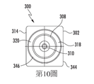
現參看第8~10圖,描繪例示性RF連接器插腳組合件300。RF連接器插腳組合件300包括了類似於如上針對第3~7圖所討論之RF連接器插腳組合件200及200'的某些態樣。因此,除了任何實質上的差異外,在此針對RF連接器插腳組合件300將不再重複此類與RF連接器插腳組合件200及200'類似之態樣的討論。Referring now to Figures 8-10, an exemplary RF
第8圖是RF連接器插腳組合件300的分解截面圖,其圖示沿著相同軸「X2
」對齊的一外殼302、一第一介電體304、一第二介電體306、一襯套308及一接觸插腳310。第9圖是經組裝之RF連接器插腳組合件300的詳細截面圖,其中接觸插腳310位於一第一方向行進極限312處。現繼續參看第8及9圖,外殼302包括一第一節314及一第二節316,第二節316由一分隔件318從第一節314隔開。分隔件318中的一出入開口320延伸在第一節314與第二節316之間。第一介電體304、第二介電體306及襯套308經定位在第二節316中,使得第一介電體304中的一第一貫穿通道322、第二介電體306中的一第二貫穿通道324及襯套308中的一襯套開口326全部對齊。第二節316包括相對於分隔件318的一開放遠端348。第一介電體304上的一第一停止表面328及第二介電體306上的一第二停止表面330界定一間隙332,其中第一停止表面328藉由間隙332來與第二停止表面330隔開一距離「A」。雖然第一介電體304的一側331在第9圖中顯示為鄰接第二介電體306,在第一停止表面328與第二停止表面330之間維持著間隙332的形成,由側331所分界。第一介電體304及第二介電體306可由任何適當材料製成,像是PTFE或Torlon(聚醯亞胺醯亞胺)之非設限性例子。FIG. 8 is an exploded cross-sectional view of the RF
接觸插腳310包括一第一插腳分段334、一第二插腳分段336及位於第一插腳分段334及第二插腳分段336之交界340處的一環狀卡圈338。第二插腳分段336可遠端終止在一連接零件342中。RF連接器插腳組合件300的組裝可藉由將第二介電體306摩擦適配在第二節316中;將第二插腳分段336插入第二介電體306的第二貫穿通道324中;將第一介電體304定位在第二節316中使得第一插腳分段334插入第一介電體304的第一貫穿通道322中且環狀卡圈338定位在間隙332中;以及將襯套308摩擦適配在第一介電體304上方的第二節316中,使得第一插腳分段334延伸通過襯套開口326。以此種方式,環狀卡圈338不需要被迫使通過第一貫穿通道322、第二貫穿通道324或襯套開口326以組裝RF連接器插腳組合件300。接觸插腳310及襯套308可由任何適當材料製成,像是鎳上金鍍黃銅的非設限性例子。The
在此方面,第一插腳分段334乃可移動地設置在第一貫穿通道322中而第二插腳分段336可移動地設置在第二貫穿通道324中,使得接觸插腳310在第一貫穿通道322及第二貫穿通道324中可在第一方向337及第二方向339中軸向移動。額外地,第一插腳分段334可延伸通過第一貫穿通道322、襯套開口326並通過出入開口320進入第一節314中。第一節314可包括具有一接收埠346的插槽344,接收埠346經調適以接收一連接器(參見例如第12圖)。第一插腳分段334可提供與插槽344之接收埠346所接收之連接器的電連續性。In this regard, the
第二節316包括相對於分隔件318的開放遠端348。第9圖中,接觸插腳310是於第一方向行進極限312處,連接零件342經定位在外殼302中。以類似於RF連接器插腳組合件200'(如第6A圖中所示)的方式,當接觸插腳310的軸向移動是在第二方向行進極限350處時,連接零件342可通過外殼302之開放遠端348延伸距離「B」,該距離「B」可小於或等於距離「A」(間隙332的尺寸)。以此方式,可提供充足的距離來允許接觸插腳310藉著其與一外部結構(像是例如PCB)的接合,而回應於連接零件342之移動而軸向地移動。更甚者,距離「B」可允許外殼302接觸PCB,使得外殼302可經調適以提供外部組件之間的接地連續性,所述外部組件例如插槽344之接收埠346所接收的連接器與該PCB。外殼302可由任何適當材料製成,像是鎳上金鍍黃銅的非設限性例子。
第10圖是往外殼302之第一節314中看的RF連接器插腳組合件300之俯瞰透視圖。接觸插腳310、分隔件318、襯套308及出入開口320為可見的,插槽344及接收埠346也是。如下將更詳細討論的,RF連接器插腳組合件300的頂部可為露出的且可觸及以允許用於連接一外部組件,像是(例如)連接器。FIG. 10 is a top perspective view of the RF
現參看第11A圖及第11B圖,圖示了例示性RF連接器插腳組合件400。RF連接器插腳組合件400包括了類似於如上針對第3~7圖所討論之RF連接器插腳組合件200、200'的某些態樣。因此,除了任何實質上的差異外,在此針對RF連接器插腳組合件400將不再重複此類與RF連接器插腳組合件200、200'類似之態樣的討論。Referring now to FIGS. 11A and 11B , an exemplary RF
第11A圖及第11B圖是經組裝之RF連接器插腳組合件400的詳細截面圖,圖示了沿著相同軸「X3
」對齊的一外殼402、一第一介電體404、一第二介電體406、及一直角接觸插腳408(也稱為直角連接器插腳)。第11A圖是經組裝之RF連接器插腳組合件400的詳細截面圖,其直角接觸插腳408於一第二方向行進極限410處。第11B圖是經組裝之RF連接器插腳組合件400的詳細截面圖,其直角接觸插腳408位於一第一方向行進極限412處。11A and 11B are detailed cross - sectional views of the assembled RF
現繼續參看第11A圖及第11B圖,外殼402 包括一第一節414及一第二節416,第二節416由一分隔件418從第一節414隔開。分隔件418中的出入開口420延伸在第一節414與第二節416之間。第一介電體404經定位在第二節416中。類似地,第二介電體406經定位在第二節416中。第一介電體404及第二介電體406可經定位在第二節416中,使得第一介電體404中的第一貫穿通道422、第二貫穿通道424及出入開口420對齊。一第一停止表面426及一第二停止表面428界定第一介電體404及第二介電體406之間的一間隙430,其中第一停止表面426由間隔430來從第二停止表面428隔開一距離「A」。第一介電體404及第二介電體406可由任何適當材料製成,像是PTFE或Torlon(聚醯亞胺醯亞胺)之非設限性例子。Continuing with FIGS. 11A and 11B , the
直角接觸插腳408包括一第一插腳分段432、一第二插腳分段434、位於第一插腳分段432及第二插腳分段434之一交界438處的一環狀卡圈436、以及與第二插腳分段434成一角度從第二插腳分段434延伸的一第三插腳分段440。特定言之,第三插腳分段440趨近垂直於第二插腳分段434(即,與第二插腳分段434成趨近直角)。第三插腳分段440整體連接至第二插腳分段434。第三插腳分段440可遠端終止在一連接零件442中。The right-
RF連接器插腳組合件400的組裝可藉由:將第一介電體404摩擦適配在第二節416中;通過第二介電體406的第二貫穿通道424插入第三插腳分段440;在第二介電體406的第二貫穿通道424中插入第二插腳分段434;以及將第二介電體406摩擦適配在第二節416中,使得第一插腳分段432插入第一介電體404的第一貫穿通道422中。以此方式,環狀卡圈436不須被迫使通過第一貫穿通道422抑或第二貫穿通道424來組裝RF連接器插腳組合件400。直角接觸插腳408可由任何適當材料製成,像是鎳上金鍍黃銅的非設限性例子。The RF
在此方面,第一插腳分段432為可移動地設置在第一貫穿通道422中而第二插腳分段434可移動地設置在第二貫穿通道424中,使得直角接觸插腳408在第一貫穿通道422及第二貫穿通道424中可在一第一方向444及一第二方向446中軸向移動。額外地,第一插腳分段432可延伸通過第一貫穿通道422並通過出入開口420進入第一節414中。第一節414可包括一插槽448,該插槽具有一接收埠450經調適以接收一連接器(參見例如第12圖)。第一插腳分段432可提供與插槽448之接收埠450所接收之連接器的電連續性。In this regard, the
第二節416包括相對於分隔件418的一開放遠端452。進一步,第二節416包括一或更多側壁通道454,該一或更多側壁通道從開放遠端452朝上延伸。尤其,第三插腳分段440經定位通過一或更多側壁通道454中至少一者,其連接零件442延伸超過第二節416至外殼402的外部。如第11B圖中顯示,當直角接觸插腳408的軸向移動於第一方向行進極限412處時,連接零件442乃外部於外殼402,第三插腳分段440的至少一部分經定位在一或更多側壁通道454內,及第三插腳分段440之遠端456的至少一部分可在外殼402中。如第11A圖中顯示,當直角接觸插腳408的軸向移動於第二方向行進極限410處時,連接零件442維持在外殼402外部,第三插腳分段440至少局部地經定位在一或更多側壁通道454內,而第三插腳分段440之遠端456的至少一部分通過外殼402之開放遠端452延伸一距離「B」。距離「B」可小於或等於距離「A」,該距離「A」是間隙430的尺寸。以此方式,可提供充足的距離來允許直角接觸插腳408藉著其與外部結構(像是例如PCB 203(見第4圖))的接合,而回應於第三插腳分段440(及連接零件442)之移動而軸向地移動。更甚者,距離「B」可允許外殼402接觸PCB 203,使得外殼402可經調適以提供在外部組件之間的接地連續性,所述外部組件例如插槽448之接收埠450所接收的連接器及PCB 203。外殼402可由任何適當材料製成,像是鎳上金鍍黃銅之非設限性例子。
第12圖是RF連接器插腳組合件300的截面圖,RF連接器插腳組合件300連接至PCB 203且具有一連接器560插入接收埠346中。RF連接器插腳組合件300與連接器560沿著相同軸「X4
」對齊。外殼302的第二節316接觸PCB 203,並藉此建立與通過外殼302之第一節314的連接器560之主體562的接地連續性。接觸插腳310之連接零件342經顯示為連接至PCB 203的一導體,其可藉由將連接零件342焊接至PCB 203上的一導電跡線(未顯示在第12圖中)來完成。環狀卡圈338經顯示位在間隙332之第一方向行進極限312處。第一插腳分段334經顯示插入連接器560中並提供與連接器560的內部導體564的連續性,以建立從PCB 203通過接觸插腳310到內部導體564的連續性。FIG. 12 is a cross-sectional view of the RF
現參看第13~14B圖,圖示例示性RF連接器插腳組合件600。RF連接器插腳組合件600包括了類似於第3~12圖之RF連接器插腳組合件200、200’、300、400的某些態樣。因此,除了任何實質上的差異外,在此針對RF連接器插腳組合件600將不再重複此類與RF連接器插腳組合件200、200’、300、400類似之態樣的討論。Referring now to FIGS. 13-14B , an exemplary RF
第13圖是RF連接器插腳組合件600的分解截面圖,圖示沿著相同軸「X5
」(也顯示在第14A~14B圖中)對齊的一外殼602、一介電體604、一襯套606、及一接觸插腳608。第14A圖是經組裝的RF連接器插腳組合件600的詳細截面圖,其接觸插腳608位於一第一位置。第6B圖是接觸插腳608位於一第二位置的經組裝RF連接器插腳組合件600之詳細截面圖。FIG. 13 is an exploded cross-sectional view of RF
現繼續參看第13~14B圖,外殼602包括一第一節610及一第二節612,其中第二節612乃藉由一分隔件614來從第一節610分開。分隔件614中的一出入開口616延伸在第一節610及第二節612之間。介電體604及襯套606經定位在第二節612中,使得介電體604中的一貫穿通道618與襯套606中的一襯套開口620全部對齊。貫穿通道618包括一內直徑TPID
並延伸在介電體604的一第一面615A與一第二面615B之間。第二節612包括相對於分隔件614的一開放遠端622。介電體604可由任何適當材料製成,像是PTFE或Torlon(聚醯亞胺醯亞胺)之非設限性例子。Now continue to refer to FIGS. 13-14B , the
接觸插腳608(也稱為軸桿)可遠端終止在一連接零件624中。接觸插腳608包括一軸桿外直徑SOD
。RF連接器插腳組合件600的組裝可藉由:摩擦適配介電體604與襯套606(例如介電體604的一外表面摩擦接合襯套606的一內表面);將襯套606摩擦適配在第二節612中(例如襯套606的一外表面摩擦接合第二節612的一內表面),使得介電體604被插入第二節612中;以及將接觸插腳608摩擦適配在介電體604的貫穿通道618中,使得接觸插腳608的至少一部分(以及連接零件624)延伸超過開放遠端622。以此方式,接觸插腳608不需要被迫使通過貫穿通道618來組裝RF連接器插腳組合件600。接觸插腳608及襯套606可由任何適當材料製成,像是鎳上金鍍黃銅之非設限性例子。The contact pin 608 (also referred to as the shaft) may terminate distally in a
在此方面,當被組裝時,襯套606將介電體604及接觸插腳608安裝在外殼602內,且也在介電體604之一外表面與外殼602之第二節612的一內表面之間提供一距離「A」。距離「A」在將介電體604及接觸插腳608組裝於外殼602之第二節612內的期間減少在接觸插腳608上的應力。額外地,當RF連接器插腳組合件600被安裝至一PCB時介電體604可因熱膨脹。距離「A」允許介電體604的徑向膨脹,進一步減少在接觸插腳608上的應力。進一步,距離「A」避免介電體604的軸向膨脹,此對維持可靠度及電性效能特性是重要的,因為RF連接器插腳組合件600的電氣特徵可依介電體604與外殼602之開放遠端622之間的距離而異。In this regard, when assembled, bushing 606 mounts
接觸插腳608可移動地設置在貫穿通道618中,使得接觸插腳608可在貫穿通道618中在第一方向626及第二方向628軸向移動。額外地,接觸插腳608的一近端630可延伸穿過貫穿通道618並通過出入開口616進入第一節610中。第一節610可包括一插槽632,該插槽具有經調適以接收一連接器(參見例如第12圖)的一接收埠634。接觸插腳608可提供與插槽632之接收埠634所接收的連接器的電連續性。The
第14A圖中,接觸插腳608位於第一位置,其連接零件624延伸超過外殼602的開放遠端622距離「B」。以此方式,可提供充足的距離來允許接觸插腳608藉著其與一外部結構的接合來回應於連接零件624的移動而軸向地移動,該外部結構像是(例如)PCB。更甚者,距離「B」可允許外殼602接觸PCB,使得外殼602可經調適以提供外部組件之間的接地連續性,所述外部組件例如插槽632之接收埠634接收的連接器以及該PCB。外殼602可由任何適當材料製成,像是鎳上金鍍黃銅之非設限性例子。In FIG. 14A, the
接觸插腳608與介電體604的摩擦接合足夠而使接觸插腳608不會隨著RF連接器插腳組合件600接合或解除接合一連接器(參見例如第12圖)而在第一方向626中移動。然而,此種摩擦接合可被有目的地或有意地克服,以改變接觸插腳608相對於介電體604及外殼602的位置。以此方式,接觸插腳608之連接零件624相對於外殼602之開放遠端622的距離允許有意的移動但避免意外的移動。The frictional engagement of the contact pins 608 with the
現參看第15A圖及第15B圖,圖示一例示性RF連接器插腳組合件700。RF連接器插腳組合件700包括類似於第3~14B圖之RF連接器插腳組合件200、200’、300、400、600的某些態樣。因此,除了任何實質上的差異外,在此針對RF連接器插腳組合件700將不再重複此類與RF連接器插腳組合件200、200’、300、400、600類似之態樣的討論。Referring now to FIGS. 15A and 15B , an exemplary RF
第15A圖是經組裝RF連接器插腳組合件700的詳細截面圖,其圖示沿著相同軸「X6
」對齊的一外殼702、一介電體704、一襯套706、及一接觸插腳708,接觸插腳708位於第一位置處。第15B圖是經組裝RF連接器插腳組合件700的詳細截面圖,其接觸插腳708位於第二位置。15A is a detailed cross-sectional view of the assembled RF
現繼續參看第15A~15B圖,外殼702包括一第一節710及一第二節712,其第二節712由一分隔件714來從第一節710分開。分隔件714中的一出入開口716延伸在第一節710與第二節712之間。介電體704及襯套706經定位在第二節712中,使得介電體704中的貫穿通道718及襯套706中的襯套開口720全部對齊。貫穿通道718包括一內直徑TPID
並延伸在介電體704的一第一面715A與一第二面715B之間。第二節712包括相對於分隔件714的一開放遠端722。介電體704可由任何適當材料製成,像是PTFE或Torlon(聚醯亞胺醯亞胺)的非設限性例子。Continuing to refer to FIGS. 15A-15B , the
接觸插腳708包括一第一插腳分段709A(也稱為軸桿)及一第二插腳分段709B(也稱為軸桿)。第一插腳分段709A及第二插腳分段709B各包括一軸桿外直徑SOD
。第二插腳分段709B與第一插腳分段709A成一角度從第一插腳分段709A延伸。特定地,第二插腳分段709B趨近垂直於的第一插腳分段709A(即,與第一插腳分段709A成趨近直角)。第二插腳分段709B經整體連接至第一插腳分段709A。第二插腳分段709B可遠端終止在一連接零件724中。The
RF連接器插腳組合件700的組裝可藉由:將介電體704與襯套706摩擦適配(例如將介電體704的一外表面摩擦接合襯套706的一內表面);將襯套706摩擦適配在第二節712中(例如襯套706的一外表面摩擦接合第二節712的一內表面)使得介電體704被插入第二節712中;以及將接觸插腳708之第一插腳分段709A摩擦適配在介電體704的貫穿通道718中,使得接觸插腳708之第一插腳分段709A的至少一部分(以及連接零件724)延伸超過開放遠端722。以此方式,接觸插腳708不需要被迫使通過貫穿通道718來組裝RF連接器插腳組合件700。接觸插腳708及襯套706可由任何適當材料製成,像是鎳上金鍍黃銅的非設限性例子。The RF
在此方面,當被組裝時,襯套706將介電體704及接觸插腳708安裝在外殼702內,並也在介電體704之一外表面與外殼702之第二節712的一內表面之間提供一距離「A」。距離「A」減少了在將介電體704及接觸插腳708組裝在外殼702之第二節712內期間在接觸插腳708上的應力。額外地,當RF連接器插腳組合件700被安裝至一PCB時介電體704可能因熱膨脹。距離「A」允許介電體704的徑向膨脹,進一步減少在接觸插腳708之第一插腳分段709A上的應力。進一步,距離「A」避免介電體704的軸向膨脹,此對於維持可靠度及電性效能特性是重要的,因為RF連接器插腳組合件700的電氣特徵可能依介電體704與外殼702之開放遠端722之間的距離而異。In this regard, when assembled, the
接觸插腳708的第一插腳分段709A可移動地設置在貫穿通道718中,使得接觸插腳708的第一插腳分段709A在貫穿通道718中可在第一方向726及第二方向728中軸向移動。額外地,接觸插腳708之第一插腳分段709A的一近端730可通過貫穿通道718延伸並通過出入開口716進入第一節710中。第一節710可包括一插槽732,該插槽具有經調適以接收一連接器(參見例如第12圖)的一接收埠734。接觸插腳708的第一插腳分段709A可提供與插槽732之接收埠734接收的連接器的電連續性。The
第二節712包括相對於分隔件714的一開放遠端722。進一步,第二節712包括從開放遠端722朝上延伸的一或更多側壁通道721。尤其,第二插腳分段709B經定位通過一或更多側壁通道721中的至少一者,連接零件724延伸穿過第二節712至外殼702的外部。
第15A圖中,接觸插腳708位於第一位置處,其第二插腳分段709B的一遠端723延伸超過外殼702的開放遠端722距離「B」,且連接零件724乃外部於外殼702。如第15B圖中顯示,當接觸插腳708的軸向移動是在第一方向726中移動時,連接零件724維持外部於外殼702,且第二插腳分段709B為至少局部地定位在一或更多側壁通道721內。以此方式,可提供充足的距離來允許接觸插腳708藉由其與一外部結構(像是例如PCB)的接合來回應於連接零件724之移動而軸向地移動。更甚者,距離「B」可允許外殼702接觸該PCB,使得外殼702可經調適以在外部組件之間提供接地連續性,所述外部組件例如插槽732之接收埠734接收的連接器及該PCB。外殼702可由任何適當材料製成,像是鎳上金鍍黃銅的非設限性例子。In FIG. 15A , the
接觸插腳708與介電體704的摩擦接合足夠而使接觸插腳708不會隨著RF連接器插腳組合件700接合或解除接合一連接器(參見例如第12圖)而在第一方向726中移動。然而,此摩擦接合可被有目的地或有意地克服,來改變接觸插腳708相對於介電體704及外殼702的位置。以此方式,接觸插腳708之連接零件724相對於外殼702之開放遠端722的距離允許故意的移動,卻避免意外的移動。The frictional engagement of the contact pins 708 with the
第16圖是連接至PCB 203之RF連接器插腳組合件600的截面圖,具有連接器560被插入接收埠634中。RF連接器插腳組合件600與連接器560沿著相同軸「X7
」對齊。外殼602的第二節612接觸PCB 203,並藉以建立與連接器560之主體562的接地連續性,該些連接器通過外殼602的第一節610。接觸插腳608的連接零件624經顯示連接至PCB 203的一導體,此可藉由將連接零件624焊接至PCB 203上的一導電跡線(未顯示在第16圖中)來完成。接觸插腳608的近端630被插入連接器560中並提供與連接器560之內部導體564的連續性,來建立從PCB 203通過接觸插腳608到內部導體564的連續性。FIG. 16 is a cross-sectional view of the RF
第17~22圖是一個多插腳RF連接器塊體組合件800的視圖。RF連接器塊體組合件800包括複數個RF連接器插腳組合件300(參見第8及9圖),該複數個RF連接器插腳組合件可移除地安裝在一連接器塊體802中。第17圖是具有多個RF連接器插腳組合件300設置其中的多插腳RF連接器塊體組合件800的俯視圖。第18圖是其中設置有連接器插腳組合件300的連接器塊體802之截面圖。第19圖是沒有RF連接器插腳組合件300的連接器塊體802之俯視圖。第20圖是沒有RF連接器插腳組合件300的連接器塊體802之截面圖。第21圖是連接至PCB 203之多插腳RF連接器塊體組合件800的俯視圖。第22圖是連接至PCB 203之多插腳RF連接器塊體組合件800的側視圖。17-22 are views of a multi-pin RF
藉由可移除地安裝複數個外殼302在複數個外殼埠804中之個別外殼埠中,各個RF連接器插腳組合件300經可移除地安裝在連接器塊體802中。應注意,儘管第17~22圖圖示了RF連接器插腳組合件300,但RF連接器插腳組合件200、200'、400、600、700也可以被可移除地安裝在連接器塊體802中,且第17~22圖的討論也適用於RF連接器插腳組合件200、200'、400、600、700。如第21及22圖中能看到的,連接器塊體802安裝至外部結構202(例如PCB 203)。外殼302可移除地安裝在外殼埠804中,使得外殼302的第二節316接觸PCB 203並藉以建立與連接器560(參見如第12圖)之主體562的接地連續性,連接器560通過外殼302的第一節314。以此種方式,外殼302中之一外殼可獨立於外殼302中之另一外殼可移除地安裝。額外地,外殼302中之一外殼中的接觸插腳310為可獨立於外殼302中之另一外殼中的接觸插腳310來在第一方向337及第二方向339(參見第9圖)軸向移動。各接觸插腳310的連接零件342(顯示在第22圖中)經連接至PCB 203的一導電跡線806(顯示在第21圖中),此可藉由將連接零件342焊接至導電跡線806來完成。更甚者,外殼302之第二節316(顯示在第22圖中)中的各者接觸PCB 203,並藉此建立外殼302與PCB 203之間的接地連續性。以此方式,RF連接器插腳組合件300可包括複數個外殼302及複數個接觸插腳310,該複數個接觸插腳利用連接器塊體802來連接至PCB 203。連接器塊體802可由任何適當塑膠材料製成並可利用任何適當的緊固件808安裝到外部結構202。Each RF
第23圖描繪一種用於組裝RF連接器插腳組合件200、200’、300、400的方法,該方法包含下列步驟:提供一外殼242、302、402,該外殼包含一第一節244、314、414、一第二節246、316、416、以及將第一節244、314、414從第二節246、316、416分開的一分隔件248、318、418(方塊900);將一第一介電體204、304、404插入外殼242、302、402的第二節246、316、416中,第一介電體204、304、404包含一第一貫穿通道208、322、422及一第一停止表面206、328、426(方塊902);將一第二介電體212、306、406插入外殼242、302、402的第二節246、316、416中,第二介電體212、306、406包含一第二貫穿通道216、324、424及一第二停止表面214、330、428,其中第二貫穿通道216、324、424對齊第一貫穿通道208、322、422且其中第一停止表面206、328、426與第二停止表面214、330、428形成一間隙220、332、430(方塊904);將一接觸插腳222、310、408可移動地定位在外殼242、302、402中,接觸插腳222、310、408包含一第一插腳分段224、334、432、一第二插腳分段226、336、434及一環狀卡圈228、338、436,該環狀卡圈位於第一插腳分段224、334、432及第二插腳分段226、336、434的交界230、340、438處,其中第一插腳分段224、334、432經可移動地設置在第一貫穿通道208、322、422中而第二插腳分段226、336、434經可移動地設置在第二貫穿通道216、324、424中,且其中接觸插腳222、310、408在第一貫穿通道208、322、422和第二貫穿通道216、324、424中可在第一方向238、337、444及第二方向240、339、446中軸向移動,及其中環狀卡圈228、338、436位在間隙220、332、430中而沒有穿過第一貫穿通道208、322、422及第二貫穿通道216、324、424(方塊906)。FIG. 23 depicts a method for assembling an RF
除非有相反地明確敘明,本文中闡述的任何方法均未有意被解讀為需要其步驟以特定順序來進行。據此,當方法請求項其實沒有敘明其步驟所欲遵從的順序時,或者在申請專利範圍或說明書中沒有相反地明確指明該些步驟被限制於一特定順序時,不應刻意推斷出任何特定順序。Unless expressly stated to the contrary, no method set forth herein is intended to be construed as requiring that its steps be performed in a particular order. Accordingly, when the method claims do not state the order in which the steps are to be followed, or when the scope of the patent application or the description does not expressly indicate that the steps are limited to a specific order, no intentional inference should be made that any specific order.
本領域中的通常知識者將顯而易見,能在不悖離本發明之精神或範疇之下進行各種修改及變化。由於本領域之技藝人士可以想出併有本發明之精神及實例的、對於所揭示實施例之組合、次組合、及變化的修改,因此本發明應被解讀為包括落在隨附申請專利範圍內的全部及其均等物。It will be apparent to those skilled in the art that various modifications and changes can be made without departing from the spirit or scope of the invention. Since those skilled in the art may devise modifications to the combinations, subcombinations, and variations of the disclosed embodiments that incorporate the spirit and examples of the invention, the invention should be construed to include those within the scope of the appended claims. all and their equivalents.
100‧‧‧浮接插腳組合件102‧‧‧插腳104‧‧‧孔106‧‧‧載座108‧‧‧軸桿110‧‧‧第一約束件112‧‧‧第二約束件114‧‧‧斜角表面116、203‧‧‧印刷電路板(PCB)200、200’‧‧‧RF連接器插腳組合件202‧‧‧外部結構204‧‧‧第一介電體206‧‧‧第一停止表面208‧‧‧第一貫穿通道210‧‧‧上表面212‧‧‧第二介電體214‧‧‧第二停止表面216‧‧‧第二貫穿通道218‧‧‧下表面220‧‧‧間隙222‧‧‧接觸插腳224‧‧‧第一插腳分段226‧‧‧第二插腳分段228‧‧‧環狀卡圈230‧‧‧交界232‧‧‧連接零件234‧‧‧第一側236‧‧‧第二側238‧‧‧第一方向239‧‧‧第一方向行進極限240‧‧‧第二方向241‧‧‧第二方向行進極限242‧‧‧外殼244‧‧‧第一節246‧‧‧第二節248‧‧‧分隔件250‧‧‧出入開口252‧‧‧插槽254‧‧‧接收埠256‧‧‧開放遠端300‧‧‧RF連接器插腳組合件302‧‧‧外殼304‧‧‧第一介電體306‧‧‧第二介電體308‧‧‧襯套310‧‧‧接觸插腳312‧‧‧第一方向行進極限314‧‧‧第一節316‧‧‧第二節318‧‧‧分隔件320‧‧‧出入開口322‧‧‧第一貫穿通道324‧‧‧第二貫穿通道326‧‧‧襯套開口328‧‧‧第一停止表面330‧‧‧第二停止表面331‧‧‧側332‧‧‧間隙334‧‧‧第一插腳分段336‧‧‧第二插腳分段337‧‧‧第一方向338‧‧‧環狀卡圈339‧‧‧第二方向340‧‧‧交界342‧‧‧連接零件344‧‧‧插槽346‧‧‧接收埠348‧‧‧開放遠端350‧‧‧第二方向行進極限400‧‧‧RF連接器插腳組合件402‧‧‧外殼404‧‧‧第一介電體406‧‧‧第二介電體408‧‧‧直角接觸插腳410‧‧‧第二方向行進極限412‧‧‧第一方向行進極限414‧‧‧第一節416‧‧‧第二節418‧‧‧分隔件420‧‧‧出入開口422‧‧‧第一貫穿通道424‧‧‧第二貫穿通道426‧‧‧第一停止表面428‧‧‧第二停止表面430‧‧‧間隙432‧‧‧第一插腳分段434‧‧‧第二插腳分段436‧‧‧環狀卡圈438‧‧‧交界440‧‧‧第三插腳分段442‧‧‧連接零件444‧‧‧第一方向446‧‧‧第二方向448‧‧‧插槽450‧‧‧接收埠452‧‧‧開放遠端454‧‧‧側壁通道456‧‧‧遠端560‧‧‧連接器562‧‧‧主體564‧‧‧內部導體600‧‧‧RF連接器插腳組合件602‧‧‧外殼604‧‧‧介電體606‧‧‧襯套608‧‧‧接觸插腳610‧‧‧第一節612‧‧‧第二節614‧‧‧分隔件615A‧‧‧第一面615B‧‧‧第二面616‧‧‧出入開口618‧‧‧貫穿通道620‧‧‧襯套開口622‧‧‧開放遠端624‧‧‧連接零件626‧‧‧第一方向628‧‧‧第二方向630‧‧‧近端632‧‧‧插槽634‧‧‧接收埠700‧‧‧RF連接器插腳組合件702‧‧‧外殼704‧‧‧介電體706‧‧‧襯套708‧‧‧接觸插腳709A‧‧‧第一插腳分段709B‧‧‧第二插腳分段710‧‧‧第一節712‧‧‧第二節714‧‧‧分隔件715A‧‧‧第一面715B‧‧‧第二面716‧‧‧出入開口718‧‧‧貫穿通道720‧‧‧襯套開口721‧‧‧側壁通道722‧‧‧開放遠端723‧‧‧遠端724‧‧‧連接零件726‧‧‧第一方向728‧‧‧第二方向730‧‧‧近端732‧‧‧插槽734‧‧‧接收埠800‧‧‧多插腳RF連接器塊體組合件802‧‧‧連接器塊體804‧‧‧外殼埠806‧‧‧導電跡線808‧‧‧緊固件900、902、904、906‧‧‧方塊AOD‧‧‧環狀卡圈的外直徑SID‧‧‧軸桿的內直徑SOD‧‧‧軸桿的外直徑TPID‧‧‧貫穿通道的內直徑FID‧‧‧貫穿通道的內直徑A、B‧‧‧距離X1、X2、X3、X4、X5、X6、X7‧‧‧軸100‧‧‧Floating pin assembly 102‧‧‧pin 104‧‧‧hole 106‧‧‧carrier 108‧‧‧shaft 110‧‧‧first restraint 112‧‧‧second restraint 114‧‧ ‧Beveled Surface 116, 203 ‧‧‧Printed Circuit Board (PCB) 200, 200'‧‧‧RF Connector Pin Assembly 202‧‧‧Outer Structure 204‧‧‧First Dielectric Body 206‧‧‧First Stop surface 208‧‧‧first through channel 210‧‧‧upper surface 212‧‧‧second dielectric body 214‧‧‧second stop surface 216‧‧‧second through channel 218‧‧‧lower surface 220‧‧ ‧Gap 222‧‧‧contact pin 224‧‧‧first pin segment 226‧‧‧second pin segment 228‧‧‧ring collar 230‧‧‧junction 232‧‧‧connecting part 234‧‧‧th One side 236‧‧‧Second side 238‧‧‧First direction 239‧‧‧First direction travel limit 240‧‧‧Second direction 241‧‧‧Second direction travel limit 242‧‧‧Shell 244‧‧‧ First Section 246‧‧‧Second Section 248‧‧‧Separator 250‧‧‧Access Opening 252‧‧‧Slot 254‧‧‧Receiving Port 256‧‧‧Open Remote 300‧‧‧RF Connector Pin Combination Part 302‧‧‧shell 304‧‧‧first dielectric body 306‧‧‧second dielectric body 308‧‧‧bush 310‧‧‧contact pin 312‧‧‧travel limit in first direction 314‧‧‧th The first section 316‧‧‧the second section 318‧‧‧partition 320‧‧‧access opening 322‧‧‧first through channel 324‧‧‧second through channel 326‧‧‧bush opening 328‧‧‧first Stop Surface 330‧‧‧Second Stop Surface 331‧‧‧Side 332‧‧‧Gap 334‧‧‧First Pin Segment 336‧‧‧Second Pin Segment 337‧‧‧First Direction 338‧‧‧Ring Shape collar 339‧‧‧Second direction 340‧‧‧Junction 342‧‧‧Connection part 344‧‧‧Slot 346‧‧‧Receiving port 348‧‧‧Open remote end 350‧‧‧Second direction travel limit 400 ‧‧‧RF connector pin assembly 402‧‧‧Shell 404‧‧‧First dielectric body 406‧‧‧Second dielectric body 408‧‧‧Right angle contact pin 410‧‧‧Second direction travel limit 412‧ ‧‧first direction travel limit 414‧‧‧first section 416‧‧‧second section 418‧‧‧divider 420‧‧‧access opening 422‧‧‧first through passage 424‧‧‧second through passage 426 ‧‧‧First Stop Surface 428‧‧‧Second Stop Surface 430‧‧‧Gap 432‧‧‧First Pin Segment 434‧‧‧Second Pin Segment 436‧‧‧Ring Collar 438‧‧‧ Junction 440‧‧‧Third Pin Segment 442‧‧‧Connection Part 444‧‧‧First Direction 446‧‧‧Second Direction 448‧‧‧Slot 450‧‧ ‧Receiving Port 452‧‧‧Open Remote 454‧‧‧Sidewall Channel 456‧‧‧Remote 560‧‧‧Connector 562‧‧‧Body 564‧‧‧Inner Conductor 600‧‧‧RF Connector Pin Assembly 602 ‧‧‧Shell 604‧‧‧Dielectric 606‧‧‧Sleeve 608‧‧‧Contact Pin 610‧‧‧First Section 612‧‧‧Second Section 614‧‧‧Separator 615A‧‧‧First Side 615B‧‧‧second face 616‧‧‧access opening 618‧‧‧through channel 620‧‧‧bush opening 622‧‧‧open distal end 624‧‧‧connecting part 626‧‧‧first direction 628‧‧‧ Second Direction 630‧‧‧Proximity 632‧‧‧Slot 634‧‧‧Receiving Port 700‧‧‧RF Connector Pin Assembly 702‧‧‧Shell 704‧‧‧Dielectric Body 706‧‧‧Bushing 708 ‧‧‧Contact pin 709A‧‧‧First pin segment 709B‧‧‧Second pin segment 710‧‧‧First segment 712‧‧‧Second segment 714‧‧Separator 715A‧‧First side 715B‧‧‧Second side 716‧‧‧Access opening 718‧‧‧Through channel 720‧‧‧Bushing opening 721‧‧‧Side wall channel 722‧‧‧Open distal end 723‧‧‧Distal end 724‧‧‧connection Part 726‧‧‧First direction 728‧‧‧Second direction 730‧‧‧Proximity 732‧‧‧Socket 734‧‧‧Receiving port 800‧‧‧Multi-pin RF connector block assembly 802‧‧‧ Connector block 804‧‧‧shell port 806‧‧‧conductive trace 808‧‧‧fastener 900, 902, 904, 906‧‧‧block A OD ‧‧‧outer diameter of ring collar S ID ‧‧ ‧Inner diameter S OD of the shaft ‧‧Outer diameter TP ID of the shaft ‧‧Inner diameter F ID of the through channel ‧‧Inner diameter A, B of the through channel ‧‧‧Distance X 1 , X 2 , X 3 , X 4 , X 5 , X 6 , X 7 ‧‧‧axis
第1圖是習用浮接插腳的局部截面圖;Figure 1 is a partial cross-sectional view of a conventional floating pin;
第2圖是接合印刷電路板(PCB)之多個習用浮接插腳的局部截面圖;Figure 2 is a partial cross-sectional view of a plurality of conventional floating pins engaging a printed circuit board (PCB);
第3圖是射頻(RF)連接器插腳組合件之單插腳配置方式的例示實施例的局部詳細視圖,該RF連接器插腳組合件具有一連接器插腳及介電體;Figure 3 is a partial detailed view of an exemplary embodiment of a single pin configuration of a radio frequency (RF) connector pin assembly having a connector pin and a dielectric body;
第4圖是接合一PCB的第3圖之RF連接器插腳組合件的多插腳配置方式之局部截面圖;Figure 4 is a partial cross-sectional view of a multi-pin configuration of the RF connector pin assembly of Figure 3 engaging a PCB;
第5圖是第3圖之RF連接器插腳組合件的例示實施例之分解截面圖,該RF連接器插腳組合件也具有外殼;Figure 5 is an exploded cross-sectional view of an exemplary embodiment of the RF connector pin assembly of Figure 3, also having a housing;
第6A圖及第6B圖是第5圖之RF連接器插腳組合件經組裝的詳細截面圖;Figures 6A and 6B are assembled detailed cross-sectional views of the RF connector pin assembly of Figure 5;
第7圖是第5圖之RF連接器插腳組合件的俯瞰透視圖;Figure 7 is a top perspective view of the RF connector pin assembly of Figure 5;
第8圖是RF連接器插腳組合件之另一例示實施例的分解截面圖,該RF連接器插腳組合件具有一連接器插腳、介電體、及一外殼;Figure 8 is an exploded cross-sectional view of another exemplary embodiment of an RF connector pin assembly having a connector pin, a dielectric body, and a housing;
第9圖是第8圖之RF連接器插腳組合件經組裝的詳細截面圖;Figure 9 is a detailed cross-sectional view of the assembled RF connector pin assembly of Figure 8;
第10圖是第8及9圖之RF連接器插腳組合件的俯瞰透視圖;Figure 10 is a top perspective view of the RF connector pin assembly of Figures 8 and 9;
第11A圖及第11B圖是經組裝之RF連接器插腳組合件之例示實施例的詳細截面圖,其具有一直角連接器插腳、介電體、及一外殼;11A and 11B are detailed cross-sectional views of an exemplary embodiment of an assembled RF connector pin assembly having right-angle connector pins, dielectric body, and a housing;
第12圖是第8圖之RF連接器插腳組合件的截面圖,該RF連接器插腳組合件經連接至一印刷電路板(PCB)且附接有一連接器;Figure 12 is a cross-sectional view of the RF connector pin assembly of Figure 8 connected to a printed circuit board (PCB) with a connector attached;
第13圖是RF連接器插腳組合件之另一例示實施例的分解截面圖,該RF連接器插腳組合件具有一連接器插腳、一介電體及一外殼;Figure 13 is an exploded cross-sectional view of another exemplary embodiment of an RF connector pin assembly having a connector pin, a dielectric body, and a housing;
第14A圖及第14B圖是第13圖之RF連接器插腳組合件經組裝的詳細截面圖;Figures 14A and 14B are assembled detailed cross-sectional views of the RF connector pin assembly of Figure 13;
第15A圖及第15B圖是一經組裝RF連接器插腳組合件的另一例示實施例的詳細截面圖,該RF連接器插腳組合件具有一直角連接器插腳、一介電體及一外殼;15A and 15B are detailed cross-sectional views of another exemplary embodiment of an assembled RF connector pin assembly having right-angle connector pins, a dielectric body, and a housing;
第16圖是第13圖之RF連接器插腳組合件的截面圖,該RF連接器插腳組合件經連接至一PCB且附接有一連接器;Figure 16 is a cross-sectional view of the RF connector pin assembly of Figure 13 connected to a PCB with a connector attached;
第17圖是一多插腳RF連接器塊體組合件之例示實施例的俯視圖,該多插腳RF連接器塊體組合件具有多個RF連接器插腳組合件設置在其中;Figure 17 is a top view of an illustrative embodiment of a multi-pin RF connector block assembly having a plurality of RF connector pin assemblies disposed therein;
第18圖是第17圖之多插腳RF連接器塊體組合件沿直線18-18切開的截面圖;Figure 18 is a cross-sectional view of the multi-pin RF connector block assembly of Figure 17 cut along line 18-18;
第19圖是第17圖之連接器塊體組合件沒有RF連接器插腳組合件下的俯視圖;Figure 19 is a top view of the connector block assembly of Figure 17 without the RF connector pin assembly;
第20圖是第19圖之連接器塊體組合件沿直線20-20切開的截面圖;Figure 20 is a cross-sectional view of the connector block assembly of Figure 19 cut along the line 20-20;
第21圖是連接至一PCB的第17圖之多插腳RF連接器塊體組合件之俯視圖;Figure 21 is a top view of the multi-pin RF connector block assembly of Figure 17 connected to a PCB;
第22圖是第21圖之多插腳RF連接器塊體組合件的側視圖;及Figure 22 is a side view of the multi-pin RF connector block assembly of Figure 21; and
第23圖是一流程圖,描繪用於組裝一RF連接器插腳組合件的例示性程序。Figure 23 is a flowchart depicting an exemplary procedure for assembling an RF connector pin assembly.
國內寄存資訊 (請依寄存機構、日期、號碼順序註記) 無Domestic deposit information (please note in order of depositor, date, and number) None
國外寄存資訊 (請依寄存國家、機構、日期、號碼順序註記) 無Overseas storage information (please note in order of storage country, institution, date, number) None
100‧‧‧浮接插腳組合件 100‧‧‧Floating pin assembly
102‧‧‧插腳 102‧‧‧Pin
104‧‧‧孔 104‧‧‧hole
106‧‧‧載座 106‧‧‧seat
108‧‧‧軸桿 108‧‧‧Shaft
110‧‧‧第一約束件 110‧‧‧First constraint
112‧‧‧第二約束件 112‧‧‧The second constraint
114‧‧‧斜角表面 114‧‧‧Beveled surface
116‧‧‧印刷電路板(PCB) 116‧‧‧Printed Circuit Board (PCB)
Claims (33)
Applications Claiming Priority (2)
| Application Number | Priority Date | Filing Date | Title |
|---|---|---|---|
| US15/581,891 US9960507B1 (en) | 2017-04-28 | 2017-04-28 | Radio frequency (RF) connector pin assembly |
| US15/581,891 | 2017-04-28 |
Publications (2)
| Publication Number | Publication Date |
|---|---|
| TW201842716A TW201842716A (en) | 2018-12-01 |
| TWI786100B true TWI786100B (en) | 2022-12-11 |
Family
ID=62016513
Family Applications (1)
| Application Number | Title | Priority Date | Filing Date |
|---|---|---|---|
| TW107111113A TWI786100B (en) | 2017-04-28 | 2018-03-30 | Radio frequency (rf) connector pin assembly |
Country Status (5)
| Country | Link |
|---|---|
| US (1) | US9960507B1 (en) |
| EP (1) | EP3616267B1 (en) |
| CN (1) | CN110622362B (en) |
| TW (1) | TWI786100B (en) |
| WO (1) | WO2018200116A1 (en) |
Families Citing this family (1)
| Publication number | Priority date | Publication date | Assignee | Title |
|---|---|---|---|---|
| CN113767530A (en) * | 2019-03-11 | 2021-12-07 | 申泰公司 | Impedance controlled electrical contact |
Citations (2)
| Publication number | Priority date | Publication date | Assignee | Title |
|---|---|---|---|---|
| US5769652A (en) * | 1996-12-31 | 1998-06-23 | Applied Engineering Products, Inc. | Float mount coaxial connector |
| TWI571014B (en) * | 2014-12-19 | 2017-02-11 | 宣德科技股份有限公司 | Manufacturing method of radio frequency connector |
Family Cites Families (22)
| Publication number | Priority date | Publication date | Assignee | Title |
|---|---|---|---|---|
| US3764959A (en) * | 1972-07-18 | 1973-10-09 | Astrolab | Universal coaxial cable connector |
| US4187481A (en) * | 1977-12-23 | 1980-02-05 | Bunker Ramo Corporation | EMI Filter connector having RF suppression characteristics |
| US4657323A (en) * | 1986-01-27 | 1987-04-14 | Itt Corporation | D-subminature filter connector |
| US4968263A (en) * | 1990-03-28 | 1990-11-06 | Molex Incorporated | Multi-pin electrical connector with floating terminal pins |
| US5169347A (en) * | 1991-10-15 | 1992-12-08 | Molex Incorporated | Slip-off electrical connector header |
| US5683255A (en) * | 1993-12-03 | 1997-11-04 | Menze; Marion John | Radio frequency connector assembly |
| US5850693A (en) | 1995-01-31 | 1998-12-22 | Berg Technology, Inc. | Method of manufacturing an array of surface mount contacts |
| US5563562A (en) * | 1995-03-24 | 1996-10-08 | Itt Industries, Inc. | RF feed-through connector |
| DE19653676C1 (en) * | 1996-12-16 | 1998-01-29 | Siemens Ag | Connection between medium voltage switch zones |
| CA2365404C (en) * | 1999-03-02 | 2008-02-12 | Huber + Suhner Ag | Coaxial connection for a printed circuit board |
| US6659786B2 (en) * | 2001-04-25 | 2003-12-09 | Tyco Electronics Amp Gmbh | Electrical connector |
| CA2453637C (en) * | 2003-12-18 | 2009-04-07 | Weco Electrical Connectors Inc. | Self-locking terminal pin |
| GB2417618B (en) * | 2004-08-31 | 2009-03-04 | Itt Mfg Enterprises Inc | Coaxial connector |
| US7607929B1 (en) * | 2008-06-30 | 2009-10-27 | Tyco Electronics Corporation | Electrical connector assembly having spring loaded electrical connector |
| KR20100086881A (en) * | 2009-01-23 | 2010-08-02 | 삼성전자주식회사 | Backlight assembly and liquid crystal display having the same |
| US7857669B1 (en) * | 2009-08-05 | 2010-12-28 | Hamilton Sundstrand Corporation | High power electrical interface connection |
| US9444197B2 (en) * | 2012-03-19 | 2016-09-13 | Holland Electronics, Llc | Shielded and multishielded coaxial connectors |
| US9112323B2 (en) * | 2012-03-19 | 2015-08-18 | Holland Electronics, Llc | Shielded and multishielded coaxial connectors |
| WO2014043398A1 (en) * | 2012-09-12 | 2014-03-20 | Hypertronics Corporation | Self-adjusting coaxial contact |
| US9356374B2 (en) * | 2013-01-09 | 2016-05-31 | Amphenol Corporation | Float adapter for electrical connector |
| US9735521B2 (en) * | 2013-01-09 | 2017-08-15 | Amphenol Corporation | Float adapter for electrical connector |
| US9362633B2 (en) * | 2013-11-07 | 2016-06-07 | Pds Electronics, Inc. | Hybridized coaxial cable connector |
-
2017
- 2017-04-28 US US15/581,891 patent/US9960507B1/en active Active
-
2018
- 2018-03-28 CN CN201880031910.2A patent/CN110622362B/en active Active
- 2018-03-28 WO PCT/US2018/024808 patent/WO2018200116A1/en not_active Ceased
- 2018-03-28 EP EP18721190.9A patent/EP3616267B1/en active Active
- 2018-03-30 TW TW107111113A patent/TWI786100B/en active
Patent Citations (2)
| Publication number | Priority date | Publication date | Assignee | Title |
|---|---|---|---|---|
| US5769652A (en) * | 1996-12-31 | 1998-06-23 | Applied Engineering Products, Inc. | Float mount coaxial connector |
| TWI571014B (en) * | 2014-12-19 | 2017-02-11 | 宣德科技股份有限公司 | Manufacturing method of radio frequency connector |
Also Published As
| Publication number | Publication date |
|---|---|
| CN110622362B (en) | 2022-06-28 |
| CN110622362A (en) | 2019-12-27 |
| WO2018200116A1 (en) | 2018-11-01 |
| TW201842716A (en) | 2018-12-01 |
| US9960507B1 (en) | 2018-05-01 |
| EP3616267B1 (en) | 2025-05-28 |
| EP3616267A1 (en) | 2020-03-04 |
Similar Documents
| Publication | Publication Date | Title |
|---|---|---|
| CN110710058B (en) | Multipin Connector Plug Block Assembly | |
| US9735531B2 (en) | Float adapter for electrical connector and method for making the same | |
| US6827608B2 (en) | High frequency, blind mate, coaxial interconnect | |
| US20180026409A1 (en) | High frequency miniature connectors with canted coil springs and related methods | |
| CN110277683B (en) | Connectors and Receptacles | |
| JP2006066384A (en) | Coaxial connector for board-to-board connection | |
| CN105359344B (en) | Plug-in connector | |
| CN108023250A (en) | adapter, socket and connector combination | |
| CN108496281A (en) | Self-closing contact sleeve | |
| CN111919344B (en) | RF connector including a flat center contact forked at the end to receive contact pins of a complementary connector and a solid insulating structure configured to guide the contact pins | |
| WO2023185088A1 (en) | Floating radio-frequency connector and floating radio-frequency connector with tolerance offset matching | |
| JP2007503591A (en) | Coaxial probe interface | |
| TWI786100B (en) | Radio frequency (rf) connector pin assembly | |
| EP3208894B1 (en) | Float adapter for electrical connector and method for making the same | |
| CN111213292B (en) | Printed circuit board plug connector with shielding element | |
| TW201347319A (en) | Coaxial connector | |
| CN210866559U (en) | Coaxial Connectors and Board-to-Board Connector Assemblies | |
| KR200496820Y1 (en) | Rf connector | |
| CN111355093B (en) | Coaxial Connectors | |
| TWI847353B (en) | Connector | |
| CN121394990A (en) | Radio frequency connector and radio frequency connecting assembly | |
| HK1244357A1 (en) | Float adapter for electrical connector and method for making the same | |
| HK1244357B (en) | Float adapter for electrical connector and method for making the same | |
| HK1199772B (en) | Electrical connector assembly with high float bullet adapter |