TWI764930B - Integrated epitaxial metal electrodes - Google Patents
Integrated epitaxial metal electrodes Download PDFInfo
- Publication number
- TWI764930B TWI764930B TW106132460A TW106132460A TWI764930B TW I764930 B TWI764930 B TW I764930B TW 106132460 A TW106132460 A TW 106132460A TW 106132460 A TW106132460 A TW 106132460A TW I764930 B TWI764930 B TW I764930B
- Authority
- TW
- Taiwan
- Prior art keywords
- layer
- metal
- layered structure
- rare earth
- metal layer
- Prior art date
Links
Images


Classifications
-
- H10D64/01302—
-
- H—ELECTRICITY
- H10—SEMICONDUCTOR DEVICES; ELECTRIC SOLID-STATE DEVICES NOT OTHERWISE PROVIDED FOR
- H10D—INORGANIC ELECTRIC SEMICONDUCTOR DEVICES
- H10D64/00—Electrodes of devices having potential barriers
- H10D64/60—Electrodes characterised by their materials
- H10D64/66—Electrodes having a conductor capacitively coupled to a semiconductor by an insulator, e.g. MIS electrodes
- H10D64/68—Electrodes having a conductor capacitively coupled to a semiconductor by an insulator, e.g. MIS electrodes characterised by the insulator, e.g. by the gate insulator
- H10D64/681—Electrodes having a conductor capacitively coupled to a semiconductor by an insulator, e.g. MIS electrodes characterised by the insulator, e.g. by the gate insulator having a compositional variation, e.g. multilayered
-
- H—ELECTRICITY
- H10—SEMICONDUCTOR DEVICES; ELECTRIC SOLID-STATE DEVICES NOT OTHERWISE PROVIDED FOR
- H10D—INORGANIC ELECTRIC SEMICONDUCTOR DEVICES
- H10D64/00—Electrodes of devices having potential barriers
- H10D64/60—Electrodes characterised by their materials
- H10D64/66—Electrodes having a conductor capacitively coupled to a semiconductor by an insulator, e.g. MIS electrodes
- H10D64/68—Electrodes having a conductor capacitively coupled to a semiconductor by an insulator, e.g. MIS electrodes characterised by the insulator, e.g. by the gate insulator
- H10D64/691—Electrodes having a conductor capacitively coupled to a semiconductor by an insulator, e.g. MIS electrodes characterised by the insulator, e.g. by the gate insulator comprising metallic compounds, e.g. metal oxides or metal silicates
-
- H10P14/2905—
-
- H10P14/2918—
-
- H10P14/2921—
-
- H10P14/2926—
-
- H10P14/3234—
-
- H10P14/3238—
-
- H10P14/3241—
-
- H10P14/3248—
-
- H10P14/3251—
-
- H10P14/3402—
-
- H10P14/6349—
-
- H10P14/6903—
-
- H10P14/69391—
Landscapes
- Engineering & Computer Science (AREA)
- Manufacturing & Machinery (AREA)
- Microelectronics & Electronic Packaging (AREA)
- Physics & Mathematics (AREA)
- Condensed Matter Physics & Semiconductors (AREA)
- General Physics & Mathematics (AREA)
- Power Engineering (AREA)
- Computer Hardware Design (AREA)
- Chemical & Material Sciences (AREA)
- Materials Engineering (AREA)
- Recrystallisation Techniques (AREA)
- Crystallography & Structural Chemistry (AREA)
- Electrodes Of Semiconductors (AREA)
- Insulated Gate Type Field-Effect Transistor (AREA)
- Crystals, And After-Treatments Of Crystals (AREA)
Abstract
Description
相關申請案之交互參照。 Cross-references to related applications.
本申請專利範圍依35 U.S.C.§ 119(e)於2016年9月22日提交之美國臨時申請案62/398,416號,其全部內容通過參考併入本文。 The scope of this application is US Provisional Application No. 62/398,416, filed on September 22, 2016, under 35 U.S.C. § 119(e), the entire contents of which are incorporated herein by reference.
本申請涉及半導體設計,並更具體地涉及用於集成外延金屬電極的分層結構,其中外延金屬被引入到下外延氧化物和上外延半導體之間。 The present application relates to semiconductor design, and more particularly to layered structures for integrating epitaxial metal electrodes, wherein epitaxial metal is introduced between a lower epitaxial oxide and an upper epitaxial semiconductor.
磊晶、外延生長及外延沉積,涉及到在結晶基底上生長或沉積結晶層。結晶層是指外延層。結晶基底作為模板並確定結晶層的方向和晶格間距。在一些實施例中,結晶層是可以晶格匹配或晶格重合。晶格匹配的結晶層可具有與結晶基底的頂面相同或非常相似的晶格間隔。晶格重合結晶層可具有晶格間距是結晶基底的晶格間距的整數倍。磊晶的品質部分基於結晶層的結晶度。實際上,高品質的外延層將是具有最小缺陷和幾乎沒有晶界的單晶。傳統上,金屬接觸層在上游處理中的某處被施加到外延結構。由於今天的複雜外延結構通常具有多於一種的器件功能,因此這可能需要在具有大量形貌的晶片上進行大量的金屬蝕刻和金屬沉積。 Epitaxy, epitaxial growth, and epitaxial deposition involve growing or depositing a crystalline layer on a crystalline substrate. The crystalline layer refers to an epitaxial layer. The crystalline substrate acts as a template and determines the orientation and lattice spacing of the crystalline layer. In some embodiments, the crystalline layer may be lattice matched or lattice coincident. The lattice matched crystalline layer may have the same or very similar lattice spacing as the top surface of the crystalline substrate. The lattice coincident crystalline layer may have a lattice spacing that is an integral multiple of the lattice spacing of the crystalline substrate. The quality of epitaxy is based in part on the crystallinity of the crystalline layer. In fact, a high-quality epitaxial layer will be a single crystal with minimal defects and few grain boundaries. Traditionally, the metal contact layer is applied to the epitaxial structure somewhere in the upstream process. Since today's complex epitaxial structures often have more than one device function, this can require extensive metal etching and metal deposition on wafers with a large number of topographies.
金屬與半導體之間的相互作用對於器件操作而言通常是至關重要的。金屬和半導體之間的這種相互作用的一個範例發生在諸如射頻(RF)濾波器 的薄膜共振器中,其中總體聲學現象是由電極的聲波阻抗與壓電材料的聲波阻抗的乘積限定。這總結在第17圖,其繪示出不同厚度金屬電極的AlN厚度的函數的共振頻率(來自S.Tanifuji等人發表在,Proceedings 2009 IEEE International Ultrasonic Symposium,第2170頁,其全部內容透過引用併入)。在這裡,晶體品質也是重要的,因為沒有它,由於多晶金屬層中缺陷和晶界的增加效應,電阻率會隨著厚度的減小而增加。 Interactions between metals and semiconductors are often critical to device operation. An example of this interaction between metals and semiconductors occurs in radio frequency (RF) filters such as The thin-film resonator, where the overall acoustic phenomenon is defined by the product of the acoustic impedance of the electrodes and the acoustic impedance of the piezoelectric material. This is summarized in Figure 17, which plots the resonant frequency as a function of AlN thickness for metal electrodes of different thicknesses (from S. Tanifuji et al. published in, Proceedings 2009 IEEE International Ultrasonic Symposium, p. 2170, which is incorporated by reference in its entirety). enter). The crystal quality is also important here, because without it, the resistivity increases with decreasing thickness due to the increasing effects of defects and grain boundaries in the polycrystalline metal layer.
InP的生長在矽金屬工程基底上進行嘗試,如Zheng等人在Journal of Applied Physics,vol.111p.123112(2012)所述,其全部內容透過參考併入本文。然而,Zheng描述的是多晶的薄膜,而不是外延的。 Growth of InP was attempted on silicon metal engineered substrates as described by Zheng et al. in Journal of Applied Physics, vol. 111 p. 123112 (2012), which is incorporated herein by reference in its entirety. However, Zheng describes polycrystalline films, not epitaxial ones.
在氧化釔穩定化氧化鋯(YSZ)上金屬的外延生長,在Gsell等人發表在Journal of Crystal Growth,vol.311,p.3731(2009),其全部內容透過參考併入本文。Gsell描述了透過使用YSZ從下面的矽基底分離金屬,因為這可以防止任何外延金屬不需要的矽化物。YSZ是使用氧化鋯和氧化釔靶材的濺射材料(或具有脈衝雷射沉積的沉積)。它不是單晶材料,具有晶界,且可是混合結晶(立方和四方)。因此,它是金屬外延生長的次優模板。另外,YSZ/矽界面的控制技術上是具有挑戰的。 Epitaxial growth of metals on yttria-stabilized zirconia (YSZ), published in Gsell et al. in Journal of Crystal Growth, vol. 311, p. 3731 (2009), which is incorporated herein by reference in its entirety. Gsell describes the use of YSZ to separate the metal from the underlying silicon substrate, as this prevents any unwanted silicide of the epitaxial metal. YSZ is a sputtering material (or deposition with pulsed laser deposition) using zirconia and yttria targets. It is not a single crystal material, has grain boundaries, and can be mixed crystals (cubic and tetragonal). Therefore, it is a suboptimal template for metal epitaxy. Additionally, the control of the YSZ/silicon interface is technically challenging.
因此,在半導體材料上外延生長具有良好晶體品質的金屬已被證明是困難的。 Therefore, epitaxial growth of metals with good crystal quality on semiconductor materials has proven difficult.
本文描述了用於在其上可以生長半導體層的分層結構中,使用集成外延金屬電極的系統和方法,。本文描述的系統和方法可包含一分層結構, 包含基底,第一稀土氧化物層外延生長在基底上、第一金屬層外延生長在稀土氧化物(REO)層上,與第一半導體層外延生長在第一金屬層上。在一些實施例中,基底包含一種或多種第IV族元素,包含但不僅限於矽(Si)、鍺(Ge)、矽上絕緣體(SOI)及矽化鍺(SiGe)。在一些實施例中,基底具有<100>或<111>的晶體方向,具有高達10度的斜切。在一些實施例中,基底包含來自第III族及第V族元素,包含但不僅限於砷化鎵(GaAs)、磷化銦(InP)、氮化鎵(GaN)。在一些實施例中,基底是另一種金屬氧化物,包含但不僅限於三氧化二鎵(Ga2O3)、三氧化二鋁(Al2O3)。 Described herein are systems and methods for using integrated epitaxial metal electrodes in a layered structure on which semiconductor layers can be grown. The systems and methods described herein may include a layered structure including a substrate on which a first rare earth oxide layer is epitaxially grown, a first metal layer epitaxially grown on a rare earth oxide (REO) layer, and a first semiconductor layer epitaxially grown on the substrate grown on the first metal layer. In some embodiments, the substrate includes one or more Group IV elements including, but not limited to, silicon (Si), germanium (Ge), silicon-on-insulator (SOI), and germanium silicide (SiGe). In some embodiments, the substrate has a crystallographic orientation of <100> or <111>, with a chamfer of up to 10 degrees. In some embodiments, the substrate includes elements from groups III and V, including but not limited to gallium arsenide (GaAs), indium phosphide (InP), gallium nitride (GaN). In some embodiments, the substrate is another metal oxide, including but not limited to gallium trioxide ( Ga2O3 ) , aluminum trioxide ( Al2O3 ) .
在一些實施例中,稀土氧化物層包含一稀土金屬元素選自週期表中鑭系元素、鈧(Sc)及釔(Y)。在一些實施例中,REO層是由具有氧與金屬比例在1和2之間的REO組成。在一些實施例中,第一金屬層包含選自週期表中過渡金屬族的金屬元素。在一些實施例中,第一半導體層包含選自第III族、第IV族、第V族的一元素。在一些實施例中,基底是由矽組成,REO層是由氧與金屬比例為1.5(ErO1.5)的氧化鉺組成,且第一金屬層是由鉬(Mo)組成。在一些實施例中,第一半導體層是由AlxSc1-xN(0
在一些實施例中,REO層包含由第一稀土氧化物(REO)組成的第一子層與由第二稀土氧化物(REO)組成的第二子層。在一些實施例中,REO層包含由第一REO組成的一第一區域與由第二REO組成的第二區域,其中第一區域以漸變的模式轉移到第二區域。在一些實施例中,REO層包含由第一REO組成的一第一子層與由第二REO組成的第二子層,且其中第一子層和第二子層以超晶格結構交替。在一些實施例中,第二金屬氧化層進一步包含第III族元素。在一些實施例中,第一金屬層包含由第一金屬組成的第一子層與由第二金屬組成的第二子層。在一些實施例中,第一金屬層包含由一第一金屬組成的一第一區域與由一第二金屬組成的一第二區域,且其中該第一區域以漸變的模式轉移到該第二區域。在一些實施例中,金屬層包含由第一金屬組成的第一子層與由第二金屬組成的第二子層,且其中第一子層和第二子層以超晶格結構交替。在一些實施例中,分層結構進一步包含在半導體層上外延生長的第二金屬層。 In some embodiments, the REO layer includes a first sublayer composed of a first rare earth oxide (REO) and a second sublayer composed of a second rare earth oxide (REO). In some embodiments, the REO layer includes a first region consisting of a first REO and a second region consisting of a second REO, wherein the first region is transferred to the second region in a gradient pattern. In some embodiments, the REO layer includes a first sublayer composed of a first REO and a second sublayer composed of a second REO, and wherein the first sublayer and the second sublayer alternate in a superlattice structure. In some embodiments, the second metal oxide layer further includes a Group III element. In some embodiments, the first metal layer includes a first sublayer composed of the first metal and a second sublayer composed of the second metal. In some embodiments, the first metal layer includes a first region composed of a first metal and a second region composed of a second metal, and wherein the first region is transferred to the second region in a graded pattern area. In some embodiments, the metal layer includes a first sublayer composed of a first metal and a second sublayer composed of a second metal, and wherein the first sublayer and the second sublayer alternate in a superlattice structure. In some embodiments, the layered structure further includes a second metal layer epitaxially grown on the semiconductor layer.
在一些實施例中,分層結構進一步包含在第二金屬層上外延生長的第二半導體層。分層結構進一步包含高達20次交替的金屬層和半導體層的組合。在一些實施例中,分層結構進一步包含金屬層和REO層的交替的組成。在一些實施例中,分層結構進一步包含第二REO層,其生長在半導體層上。在一些實施例中,第二金屬層外延生長在第二REO層上。在一些實施例中,如請求項1所述之分層結構進一步包含從第一金屬層生長的外延層,其中外延層包含選自二維(2D)材料、蓋層和絕緣體的群組的成分。在一些實施例中,二維材料是選自石墨烯和過渡金屬二硫化物的群組。在一些實施例中,蓋層是由選自金屬氧化物和金屬矽化物的群組的材
料組成。在一些實施例中,絕緣體是由REO組成。在一些實施例中,中間層,從第一金屬層轉換到第一半導體層。在一些實施例中,中間層選自金屬氮化物、金屬磷屬化物和模板2D電極的群組的一種或多種材料。
In some embodiments, the layered structure further includes a second semiconductor layer epitaxially grown on the second metal layer. The layered structure further comprises up to 20 alternating combinations of metal and semiconductor layers. In some embodiments, the layered structure further comprises alternating compositions of metal layers and REO layers. In some embodiments, the layered structure further includes a second REO layer grown on the semiconductor layer. In some embodiments, the second metal layer is epitaxially grown on the second REO layer. In some embodiments, the layered structure of
在一些實施例中,從第一REO層轉移到第一金屬層的中間層。在一些實施例中,中間層與來自第一金屬層的金屬成分與氧一起生長。在一些實施例中,第一金屬層在第一金屬層的第一部分與該第一金屬層的第二部份之間,具有含第一間隙的非連續的模式,且第一半導體層在間隙與金屬區域上生長。 In some embodiments, the intermediate layer is transferred from the first REO layer to the first metal layer. In some embodiments, the intermediate layer is grown with the metal component from the first metal layer and oxygen. In some embodiments, the first metal layer has a discontinuous pattern with a first gap between a first portion of the first metal layer and a second portion of the first metal layer, and the first semiconductor layer is in the gap grow on areas with metal.
100、300、400、500、600、700、800、900、1000、1100、1200、1202、1204、1302、1304、1306、1400、1402、1500、1600:分層結構 100, 300, 400, 500, 600, 700, 800, 900, 1000, 1100, 1200, 1202, 1204, 1302, 1304, 1306, 1400, 1402, 1500, 1600: Hierarchical structure
102:基底 102: Substrate
104:稀土氧化物層 104: Rare earth oxide layer
106、210:金屬層 106, 210: Metal layer
108:半導體層 108: Semiconductor layer
200:流程示意圖 200: Flow Diagram
302、402、406:第一金屬層 302, 402, 406: the first metal layer
304、404、408、1404、1602:第二金屬層 304, 404, 408, 1404, 1602: second metal layer
502、802:第一區域 502, 802: The first area
504、804:第二區域 504, 804: The second area
602、702、706、604、704、708:層 602, 702, 706, 604, 704, 708: Layers
1002、1102:中間層 1002, 1102: middle layer
1004:金屬氧化物 1004: Metal oxides
1106:金屬氮化物 1106: Metal Nitride
1108:稀土磷屬化物 1108: Rare earth phosphide
1110:二維(2D)電極 1110: Two-Dimensional (2D) Electrodes
1406:結構 1406: Structure
1408:第二半導體層 1408: Second semiconductor layer
1502:組合 1502: Combination
1504:堆疊 1504: Stacked
2102、2104、2106、2108:步驟 2102, 2104, 2106, 2108: Steps
本揭露的進一步特徵,結合附圖根據以下詳細描述其性質和各種優點將變得顯而易見,其中:第1圖根據說明性實施例,描繪了在基底與半導體層之間生長外延金屬之分層結構;第2圖根據說明性實施例,描繪了生長第1圖示出的分層結構之流程圖;第3圖到第16圖根據說明性實施例,描繪了分層結構的各種範例,每個都是第1圖示出的分層結構的具體範例;第17圖根據先前技術的實施例,描繪了不同厚度金屬電極的共振頻率AlN厚度的函數;第18圖描繪了計算具有和不具有外延金屬電極的分散式布拉格反射鏡(DBR)反射率,其中在標準第III族氮化物DBR之下添加結晶REO和金屬增 加峰值反射率2%;第19圖根據說明性實施例,描繪一圖表示出從AIN和GaN的11週期DBR如何建構;第20圖根據說明性實施例,描繪了在450nm處計算的反射率,其繪製了AlN-GaN的DBR與在Mo上的單對AlN上構建的AlN-GaN的DBR;以及第21圖根據說明性實施例,描繪了生長第1圖示出的分層結構圖的方法的流程圖。 Further features of the present disclosure, the nature and various advantages of which will become apparent from the following detailed description taken in conjunction with the accompanying drawings, in which: FIG. 1 depicts a layered structure for growing epitaxial metal between a substrate and a semiconductor layer, according to an illustrative embodiment. ; Figure 2 depicts a flow chart for growing the layered structure shown in Figure 1, according to an illustrative embodiment; Figures 3 to 16 depict various examples of layered structures, each according to an illustrative embodiment All are specific examples of layered structures shown in Figure 1; Figure 17 depicts the resonant frequency of metal electrodes of different thicknesses as a function of AlN thickness, according to an embodiment of the prior art; Figure 18 depicts calculations with and without epitaxy Dispersed Bragg Reflector (DBR) reflectivity of metal electrodes with addition of crystalline REO and metal enhancements under standard Group III nitride DBR plus peak reflectance 2%; Figure 19 depicts a graph showing how an 11-period DBR is constructed from AIN and GaN, according to an illustrative embodiment; Figure 20 depicts calculated reflectance at 450 nm, according to an illustrative embodiment , which plots a DBR of AlN-GaN versus a DBR of AlN-GaN built on a single pair of AlN on Mo; and Figure 21 depicts the growth of the layered structure diagram shown in Figure 1, according to an illustrative embodiment Flowchart of the method.
本文描述的結構和方法,提供了集成外延金屬電極,其在外延疊層內併入外延金屬,從而結合掩埋接觸層。本文揭露的結構和方法包含高品質外延金屬層及在外延金屬層上繼續生長半導體材料的能力。在一實施例中,一結晶REO層可在基底或半導體上外延生長,且一金屬層可在結晶REO層上外延生長。半導體層可在外延金屬層上生長。REO層是包含一種或多種稀土(RE)物質和氧。稀土物質包含鑭(La)、鈰(Ce)、鐠(Pr)、釹(Nd)、鉅(Pm)、釤(Sm)、銪(Eu)、釓(Gd)、鋱(Tb)、鏑(Dy)、鈥(Ho)、鉺(Er)、銩(Tm)、鐿(Yb)、鎦(Lu)、鈧(Sc)和釔(Y)。 The structures and methods described herein provide integrated epitaxial metal electrodes that incorporate epitaxial metal within an epitaxial stack, thereby incorporating buried contact layers. The structures and methods disclosed herein include high quality epitaxial metal layers and the ability to continue growing semiconductor materials on the epitaxial metal layers. In one embodiment, a crystalline REO layer can be epitaxially grown on the substrate or semiconductor, and a metal layer can be epitaxially grown on the crystalline REO layer. The semiconductor layer can be grown on the epitaxial metal layer. The REO layer is composed of one or more rare earth (RE) species and oxygen. Rare earth substances include lanthanum (La), cerium (Ce), pyridine (Pr), neodymium (Nd), giant (Pm), samarium (Sm), europium (Eu), gadolinium (Gd), abium (Tb), dysprosium ( Dy), ∥ (Ho), Erbium (Er), Tm (Tm), Ytterbium (Yb), Litium (Lu), Scandium (Sc), and Yttrium (Y).
REOs已知表現為螢石型結構。這些結構表現出作為存在於氧化物中的稀土陽離子的原子量的函數的形態差異,以及其他因素。 REOs are known to exhibit fluorite-type structures. These structures exhibit morphological differences as a function of the atomic weight of the rare earth cations present in the oxide, among other factors.
具體而言,包含輕稀土的氧化物形成立方CaF2型晶體結構作為可能的+2和/或+3和/或+4的離子狀態的結果。由於多種可能的氧化態(對於稀土氧化物),氧化物具有這種晶體結構表現出明顯的淨電荷缺陷。 Specifically, oxides comprising light rare earths form a cubic CaF 2 -type crystal structure as a result of possible ionic states of +2 and/or +3 and/or +4. Oxides with this crystal structure exhibit significant net charge defects due to the variety of possible oxidation states (for rare earth oxides).
另一方面,由於離子狀態為RE<+3>,由重稀土(例如:RE2O3等)形成的氧化物表現出扭曲的CaF2型晶體結構,其包含陰離子空缺。重稀土的稀土氧化物有關的晶體結構也被稱為「方鐵石」。 On the other hand, since the ionic state is RE<+3>, oxides formed from heavy rare earths (eg: RE 2 O 3 , etc.) exhibit a distorted CaF 2 -type crystal structure containing anion vacancies. The crystal structure associated with rare earth oxides of heavy rare earths is also referred to as "wispyrite".
具有RE2O3形式的稀土氧化物的說明實施例是Er2O3。Er2O3的單元晶胞的晶體結構是氧空缺衍生的螢石衍生物(即,方鐵石結構)。REO電介質層可包含這些單元晶胞的集合體。 An illustrative example of a rare earth oxide having the RE2O3 form is Er2O3 . The crystal structure of the unit cell of Er 2 O 3 is an oxygen vacancy derived fluorite derivative (ie, a waffle structure). The REO dielectric layer may comprise an aggregate of these unit cells.
陰離子空缺的數量和位置決定了RE2O3單元晶胞的晶體形狀。該晶胞的晶體形狀可被設計成提供與下面的半導體基底的晶格常數的適當匹配。氧空缺沿著體對角線和/或面對角線導致C-型立方結構。例如:每個螢石單位晶胞的兩個陰離子空缺引起Er2O3的單元晶胞增加到幾乎兩倍於Si的晶胞尺寸。這反過來,使低應變單相Er2O3能夠直接在矽基底上外延生長。 The number and position of anion vacancies determine the crystal shape of the RE2O3 unit cell. The crystal shape of the unit cell can be designed to provide an appropriate match to the lattice constant of the underlying semiconductor substrate. Oxygen vacancies along the body diagonal and/or face diagonal lead to a C-type cubic structure. For example: two anion vacancies per unit cell of fluorite cause the unit cell of Er2O3 to increase to almost twice the size of the unit cell of Si. This, in turn, enables the direct epitaxial growth of low-strain single-phase Er 2 O 3 on silicon substrates.
此外,陰離子空缺的數量和位置可設計成在介電層和/或過渡生長層中引起期望的應變(拉伸或壓縮)。例如:在一些實施例中,半導體層中的應變被期望影響載子遷移率。 Furthermore, the number and location of anion vacancies can be designed to induce a desired strain (tensile or compressive) in the dielectric layer and/or the transitional growth layer. For example: in some embodiments, strain in the semiconductor layer is expected to affect carrier mobility.
每個螢石單元晶胞具有兩個氧空缺,其位於延著體對角線上。這兩個氧空缺的存在導致Er2O3單元晶胞尺寸加倍,從而使其晶格常數加倍,其提供了<100>矽的晶格常數的適當匹配。 Each fluorite unit cell has two oxygen vacancies, which are located along the diagonal of the body. The presence of these two oxygen vacancies results in a doubling of the Er2O3 unit cell size and thus its lattice constant, which provides a suitable match for the lattice constant of <100> silicon.
在一些實施例中,氧空缺位於面對角線的兩端。在一些實施例中,氧空缺分佈在面對角線和體對角線的端部之間。 In some embodiments, the oxygen vacancies are located at opposite ends of the diagonal. In some embodiments, the oxygen vacancies are distributed between the ends of the face diagonal and the body diagonal.
在半導體層上使用金屬的外延沉積可生長掩埋的金屬接觸層。外延金屬層可直接在半導體層上和/或直接在基底上生長。在一些實施例中,可選的過渡層可在外延金屬層和下面的半導體層之間,和/或在外延金屬層和下面的 基底之間。除了掩埋接觸層所帶來的電氣優點外,金屬和可被利用的上覆的半導體之間通常存在相互作用。這些交互作用,諸如射頻濾波器中,當金屬和半導體(以及任何中間界面)之間的界面品質高而缺陷少時更有用。另外,外延金屬可製造的比濺鍍金屬薄,同時保持高薄膜品質。這部分是因為外延界面品質較高,且隨著層變薄,界面在整個材料中佔有更大的比例。因此,儘管厚膜不易受到品質差的界面的影響,而其性能主要受體材料性質的影響,薄膜的性能主要受界面性質的控制。因此,高品質界面在沉積薄膜時很重要。 A buried metal contact layer can be grown on the semiconductor layer using epitaxial deposition of metal. The epitaxial metal layer can be grown directly on the semiconductor layer and/or directly on the substrate. In some embodiments, an optional transition layer may be between the epitaxial metal layer and the underlying semiconductor layer, and/or between the epitaxial metal layer and the underlying semiconductor layer between the bases. In addition to the electrical advantages provided by buried contact layers, there is often an interaction between the metal and the overlying semiconductor that can be utilized. These interactions, such as in radio frequency filters, are more useful when the interface between the metal and semiconductor (and any intermediate interfaces) is of high quality with few defects. Additionally, epitaxial metals can be fabricated thinner than sputtered metals while maintaining high film quality. This is partly due to the higher quality of the epitaxial interface, and as the layer gets thinner, the interface occupies a larger proportion of the overall material. Thus, while thick films are less susceptible to poor-quality interfaces, while their performance is primarily influenced by material properties, thin film properties are primarily controlled by interface properties. Therefore, a high-quality interface is important when depositing thin films.
另外,可使用外延金屬層來改變層的外延堆疊的反射率。對於光發射來自頂部表面的裝置來說,朝向基底發射的光通常被認為損失了整體輸出功率。例如:在垂直共振腔面射型雷射(VCSELs),後視鏡必須具有>99.8%的反射率。這很難僅透過半導體材料來實現。 Additionally, epitaxial metal layers can be used to alter the reflectivity of the epitaxial stack of layers. For devices in which light is emitted from the top surface, the light emitted towards the substrate is generally considered to lose overall output power. For example, in vertical cavity surface emitting lasers (VCSELs), the rearview mirror must have >99.8% reflectivity. This is difficult to achieve with semiconductor materials alone.
第18圖示出一圖表描繪計算具有和不具有外延金屬電極的DBR反射率,其在標準的第III族氮化物DBR之下添加結晶的稀土氧化物和金屬增加峰值反射率2%。第III族氮化物是包含第III族物質和氮的材料。第III族物質可包含一種或多種在週期表第III族物質的元素,包含B、Al、Ga、In、與Tl。第III族氮化物層可為包含多種第III族元素的化合物。第III族氮化物層可包含二元化合物諸如GaN、三元化合物諸如AlxGa1-xN(0


結晶稀土氧化物(REO)外延層可被使用作為在半導體基底諸如矽上的外延金屬的模板。可使用除矽之外的基底,且實施例包含鍺、Si-Ge合金、藍寶石、二氧化矽、矽上絕緣體(SOI)與矽半導體(SOS),具有上述之一的頂層 的基底及任何半導體基底。就金屬磊晶而言,結晶REO與YSZ相比是一種優質材料。首先,將結晶REO和基底之間的界面設置為外延製程的一部分。在適當選擇稀土氧化物的情況下,可外延生長結晶REO模板其為100%(或接近100%)立方,沒有第二相。結晶REO的其它參數與製程特徵有利於整個外延堆疊的是氧化矽界面,其沒有任何寄生電荷,比YSZ(8.6至6.1g/cm3)更高的密度,以及比YSZ好5倍的導熱率。除了用作外延金屬生長的模板之外,結晶REO層也可防止外延金屬層和下面的任何基底之間相互擴散。例如:這可防止形成不需要的金屬矽化物(其中基底是矽)。 Crystalline rare earth oxide (REO) epitaxial layers can be used as templates for epitaxial metals on semiconductor substrates such as silicon. Substrates other than silicon can be used, and examples include germanium, Si-Ge alloys, sapphire, silicon dioxide, silicon-on-insulator (SOI), and silicon semiconductor (SOS), substrates with a top layer of one of the above, and any semiconductor base. For metal epitaxy, crystalline REO is a superior material compared to YSZ. First, the interface between the crystalline REO and the substrate is set up as part of the epitaxy process. With proper selection of rare earth oxides, it is possible to epitaxially grow crystalline REO templates that are 100% (or close to 100%) cubic with no secondary phases. Other parameters and process characteristics of crystalline REO that are beneficial to the entire epitaxial stack are the silicon oxide interface, which does not have any parasitic charges, a higher density than YSZ (8.6 to 6.1 g/cm 3 ), and 5 times better thermal conductivity than YSZ . In addition to serving as a template for epitaxial metal growth, the crystalline REO layer also prevents interdiffusion between the epitaxial metal layer and any underlying substrate. For example: this prevents the formation of unwanted metal silicides (where the substrate is silicon).
第1圖示出說明根據說明性實施例的分層結構100的示例圖。分層結構100包含基底102、在基底102上生長的REO層104、在REO層104上外延生長的金屬層106,與在金屬層106上外延生長的半導體層108。REO層104的厚度是定義為tox其中通常氧化物的厚度可被定義為0


第1圖的分層結構100可在諸如矽基底的基底102上生長。如果濾波器中的半導體材料是外延的,它有助於集成附加的半導體元件(不一定直接電連接到濾波器)可在上述濾波器上生長。例如:電晶體(其包含場效電晶體,與異質接合雙極性電晶體的範例)可在濾波器上成長,從而減少給定系統所需的晶片面積。
The
第2圖描繪了流程示意圖200,其示出製造第1圖所描繪的結構的單外延製程。結晶REO層104在基底102上外延生長。金屬層106在結晶REO層104上外延生長。半導體層108在金屬層106上外延生長。在一些實施例中,附加的金屬層210可在半導體層108上外延生長。第2圖中描繪的每個層可包含一種或多種子層。在第3圖到第13圖中更詳細描述了每個層的成分。
FIG. 2 depicts a flow diagram 200 illustrating a single epitaxy process for fabricating the structure depicted in FIG. 1 .
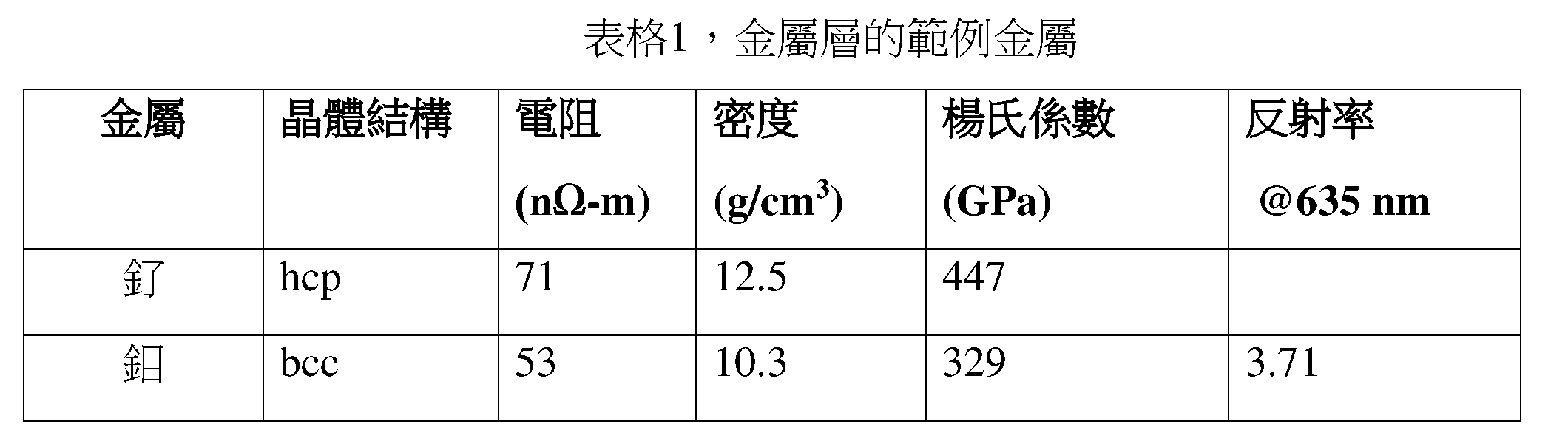
使用外延金屬可為稀土金屬或金屬例如:釕或鉬或下面表格1所列出的代表性金屬。用於選擇用於外延金屬層210的金屬元件的屬性包括電阻率,以及確定層的光學和聲學性質的密度、楊氏係數與折射率。表格1中未列出的其它金屬也可使用。
The epitaxial metal used may be a rare earth metal or a metal such as: ruthenium or molybdenum or a representative metal listed in Table 1 below. Properties used to select metal elements for

(hcp-六方最密堆積,fcc-面心立方,bcc-體心立方,dhcp-雙六方最密堆積)例如:基底102可由矽組成;REO層104可由氧與金屬比例為1.5的氧化鉺(ErO1.5)組成,與第一金屬層106可由鉬(Mo)組成。第一半導體層可由AlxSc1-xN(0
如另一個範例,基底102其由矽組成可具有<100>的方向,當REO層104由ErO1.5組成可具有<110>的晶體方向,且當第一金屬層106由Mo組成可具有晶體方向<211>。在這個範例中,REO中氧與金屬的比例可具有1.4與1.6之間的範圍,且半導體層108可具有各種成分。
As another example, the
第3到第5圖描繪了在結晶REO層104上包含多種外延金屬層的結構。在第3到第5圖中外延金屬層可包含多種金屬層。多種金屬層可如第3到第4圖中堆疊生長,例如:從一類型金屬到另一類型金屬的步階變化,或如第5圖示出的漸變變化。要注意的是,在第3到第5圖中描繪了兩個類型的金屬層僅用於
說明的目的,但兩種以上類型的金屬層可使用在類似如第3到第5圖示出的方法中的結構。
Figures 3-5 depict structures comprising various epitaxial metal layers on the
第3圖示出說明根據說明性實施例分層結構300的示例圖。分層結構300包含在REO層104上外延生長的第一金屬層302、採逐步式配置外延生長在第一金屬層302上的第二金屬層304。在一些實施例中,在第一金屬層302與第二金屬層304中的金屬可為相同的。在一些實施例中,在第一金屬層302與第二金屬層304中的金屬可為不相同的。在一些實施例中,第一金屬層302與第二金屬層304可具有相同厚度。在一些實施例中,第一金屬層302可具有不同於第二金屬層304的厚度。
FIG. 3 shows an example diagram illustrating a
第4圖示出說明根據說明性實施例分層結構400的示例圖。分層結構400包含以超晶格類型結構在REO層104上外延生長的第一金屬(層402、406)與第二金屬層(層404、408)的多個交替的層。在一些實施例中,第一金屬層402、406中與第二金屬層404、408中的金屬可為相同的。在一些實施例中,第一金屬層402、406中與第二金屬層404、408中的金屬可為不相同的。在一些實施例中,第一金屬層402、406與第二金屬層404、408可具有相同厚度。在一些實施例中,第一金屬層402、406的厚度可不同於第二金屬層404、408。應該注意的是,第4圖示出兩種不同類型的金屬層的兩次交替僅說明目的,且在這結構中可使用不同次數的交替(例如:三次、四次、五次等)。
FIG. 4 shows an example diagram illustrating a
第5圖示出說明根據說明性實施例分層結構500的示例圖。分層結構500包含在REO層104上外延生長的金屬層106,當金屬層106具有第一區域502與第二區域504其第一金屬的第一濃度與第二金屬的第二濃度已漸變配置改變。第5圖中第一和第二金屬的第一和第二濃度的梯度可為線性的(例如:從第一
金屬到第二金屬的成分的線性變化)、超線性的(例如:更高階多項式)、次線性的或階梯式的(例如:材料成分中的分離變化)。在一些實施例中,第一濃度可在第一區域502中具有第一值並在第二區域504中具有第二值。第一金屬的濃度可在遍及整個金屬層106的厚度上變化。類似地,第二金屬的第二濃度可具有第一區域502中的第三值與第二區域504中的第四值。第二金屬的濃度可在遍及整個金屬層106的厚度上變化。
FIG. 5 shows an example diagram illustrating a
分層結構300到500被描繪在第3到第5圖中描繪中,可包含在射頻(RF)濾波器。在外延金屬層106上生長的半導體層108可為充當是耦合的機電共振器的壓電材料。外延第一金屬層(302、402)可為RF濾波器的第一電極,第二金屬層(304、404)可為RF濾波器的第二電極。外延金屬層對於RF濾波器中的電極特別有用,因為它們提供具有單晶結構高導電率的金屬,其作為隨後在金屬層上生長單晶層(例如,半導體層)的模板。單晶半導體層作為RF濾波器中的半導體材料是有用的,因為它們提供了更高的壓電係數、更窄的帶寬和更低的損耗。部分提高的性能是由於外延金屬電極的品質與結晶登記,其導致後續膜的品質更高。
Layered structures 300-500, depicted in Figures 3-5, may be included in radio frequency (RF) filters. The
第3到第5圖描繪了任何結構可包含在光學裝置中。一個這樣的應用在分散式布拉格反射鏡(DBR)中。對於DBR,一個關鍵的考慮因素是組成層之間的折射率。折射率越不相同,所需的時間越短,阻帶越寬。這提供了減少總層疊厚度,從而降低製造成本/複雜性的途徑。例如:在DBR中設計半導體AIN和GaN,在420nm處折射率δ是0.34。如果兩個材料在外延Mo上變化為AIN,則這種差異將增加到0.85。 Figures 3-5 depict that any structure may be included in an optical device. One such application is in Distributed Bragg Reflectors (DBR). For DBR, a key consideration is the refractive index between the constituent layers. The more different the indices of refraction, the shorter the time required and the wider the stopband. This provides a way to reduce the overall stack thickness, thereby reducing manufacturing cost/complexity. For example: in the design of semiconductor AIN and GaN in DBR, the refractive index δ at 420nm is 0.34. This difference increases to 0.85 if the two materials are changed to AIN on epitaxial Mo.
在許多光子裝置中,所有的光不會垂直於外延表面傳播。當DBR由僅折射率差異很小的半導體構成時,反射率對入射角具有很強的依賴性。分
層結構100的反射率的性能的範例與不具有外延金屬層106的比較,在第18到20圖示出。
In many photonic devices, all light does not propagate perpendicular to the epitaxial surface. When the DBR is composed of semiconductors with only a small difference in refractive index, the reflectivity has a strong dependence on the angle of incidence. Minute
An example of the reflectivity performance of the
第6到8圖描繪了在基底102上包含多種結晶REO層104的層結構。在第6圖與第7圖中的REO層104可包含多種REO層104。任一多種稀土氧化物層可生長如第6到第7圖那樣堆疊,例如:從一種類型的REO到另一種類型的REO的一步階變化,或如第8圖示出的漸變變化。在一些實施例中,可有範例,其具有第一優化REO被放置相鄰於基底102,與第二優化REO被放置以支撐金屬層106的磊晶。僅用於說明目的,在第6到8圖中描繪的兩種類型的REO層,但如第6到8圖示出相似的方法中的結構中可使用大於兩種類型的REO層。
Figures 6-8 depict layer structures comprising various crystalline REO layers 104 on
第6圖描繪分層結構600其包含在基底102上外延生長的第一稀土氧化物層602、採逐步式的配置在第一稀土氧化物層602上外延生長的第二稀土氧化物層604。在一些實施例中,第一稀土氧化物層602與第二稀土氧化物層604中的稀土金屬可為相同的。在一些實施例中,第一稀土氧化物層602與第二稀土氧化物層604中的稀土金屬可為不相同的。在一些實施例中,第一稀土氧化物層602與第二稀土氧化物層604可具有相同的厚度。在一些實施例中,第一稀土氧化物層602與第二稀土氧化物層604可具有不相同的厚度。在一些實施例中,第一稀土金屬可具有在第一層602中的第一濃度與在第二層604中的第二濃度。類似地,第二稀土金屬可具有在第一層602中的第三濃度和在第二層604中的第四濃度。
FIG. 6 depicts a
第7圖描繪分層結構700其包含在基底102上以超晶格類型配置外延生長的第一REO(層702、706)與第二REO(層706、708)的多個交替層。在一些實施例中,第一REO層702、706與第二稀土金屬氧化物層704、708中的稀土金屬可為相同的。在一些實施例中,第一層702、706中的稀土金屬和第二層704與706中的稀土金屬可為不相同的。在一些實施例中,第一REO層702、706和第二
REO層704、708可具有相同的厚度。在一些實施例中,第一REO層702、706可具有不同於第二REO層704與708的厚度。在一些實施例中,第一稀土金屬可具有在層702中的第一濃度與在層704中的第二濃度。類似地,第二稀土金屬可具有在層702中的第三濃度與在層704中的第四濃度。在一些實施例中,在層702和層704中氧的濃度可為不相同。要注意的是,第7圖中示出兩種不同的類型的REO層的兩次交替僅用於說明的目的,而在此結構中可使用不同次數的交替(例如:三次、四次、五次等)。
FIG. 7 depicts a
第8圖示出說明根據說明性實施例的分層結構800的示例圖。分層結構800包含在基底102上外延生長的REO層104,其REO層104具有第一區域802與第二區域804其第一稀土金屬的第一濃度和第二稀土金屬的第二濃度以漸變配置改變。第8圖中的第一和第二稀土金屬的第一和第二濃度的梯度可為線性的(例如:從第一金屬到第二金屬的成分的線性變化)、超線性的(例如:更高階多項式)、次線性的或階梯式的(例如:材料成分中的分離變化)。在一些實施例中,第一稀土金屬的第一濃度可在第一區域802中具有第一值並在第二區域804中具有第二值。第一稀土金屬的濃度可在遍及整個REO層104的厚度上變化。類似地,第二稀土金屬的第二濃度可具有第一區域802中的第三值與第二區域804中的第四值。第二稀土金屬的濃度可在遍及整個REO層104的厚度上變化。
FIG. 8 shows an example diagram illustrating a
第9圖描繪示出說明根據說明性實施例的分層結構900的示例圖。分層結構900描繪第1圖示出的結構的範例,其半導體層108是第III族氮化物層,特別是Al1-xScxN(0

在一些實施例中,如第1圖示出的分層結構100可被修改以在任一外延金屬層106與半導體層108之間或REO層104與外延金屬層106之間包含中間
層。這一層的目的是允許從氧化物到金屬或金屬到半導體的轉變的化學或晶體學工程。化學工程可包含在半導體或金屬層的初始外延沉積期間促進半導體或金屬原子的成核或遷移。晶體學工程在金屬和半導體層之間可包含幫助晶體結構或晶格常數的轉變。晶體結構轉變的例子是從六方晶體結構向立方晶體結構的轉變。
In some embodiments, the
第10圖示出根據說明性實施例的分層結構1000的示例圖。分層結構1000描繪了在結晶REO層104上外延生長的中間層1002上的外延金屬層106。在一些實施例中,中間層1002可為由外延金屬層106中的金屬與氧氣的組合製成的金屬氧化物1004。
FIG. 10 shows an example diagram of a
第11圖示出說明根據說明性實施例的分層結構1100的示例圖。分層結構1100描繪了REO層104上的外延金屬層106、外延金屬層106上的外延中間層1102,與中間層1102上的外延半導體層。在一些實施例中,中間層可由金屬矽化物組成。在一些實施例中,中間層可由金屬氮化物1106組成。在一些實施例中,中間層1102可由稀土磷屬化物1108組成,其通常包含稀土氮化物、稀土砷化物與稀土磷化物。在一些實施例中,中間層1102可由二維(2D)電極1110組成。
FIG. 11 shows an example diagram illustrating a
在一些實施例中,更多不同組成/類型的半導體可在另一個半導體層108上外延生長。在一些實施例中,可在半導體層上生長第二金屬。對於這個實施例可使用任何先前描述的金屬磊晶方案,且先前描述的在金屬和半導體之間外延生長的任何中間層可用於整個外延製程,取決於最終外延疊層所需的特徵。半導體上方的層不必與半導體下方的層相匹配。例如:半導體上方的層可與半導體下方的層相同或不同
In some embodiments, more semiconductors of different compositions/types may be epitaxially grown on another
在一些實施例中,可在半導體層108上生長外延金屬層。在一些實施例中,可在半導體層108與外延金屬層之間生長三個可能的外延中間層,金屬矽化物、金屬氮化物與稀土磷化物。如果選擇在半導體層108上生長n個外延
金屬層,則為了在金屬上外延生長另一個半導體層的目的,以上任何或全部例子都可以交替。
In some embodiments, an epitaxial metal layer may be grown on the
第12圖示出說明根據說明性實施例的分層結構1202與1204的單元的組成的裝置的示例圖。分層結構1200描繪了具有可選中間層的交替金屬/半導體結構的範例。第12圖描繪了三個單元的分層結構1204。層堆疊可包含其它數量的單元,但是為了說明的目的這裡示出三個。每個單元可為相同的,或層堆疊中的一個或多個單元可為不相同的。分層結構1202描繪分層結構1204內的例示性單元。這個例示性單元包含在第一外延金屬層上外延生長的第一中間層、在第一中間層上外延生長的半導體層、在半導體層上外延生長的第二中間層,與在第二中間層上外延生長的第二外延金屬層。層堆疊內的任何單元可包括沒有、一個,或兩個第一和第二中間層。另外,一個單元中的第二外延金屬層可與上述單元中的第一外延金屬層相同。單元中的一個或兩個外延金屬層可為單金屬、漸變金屬層、具有多種子層的金屬層,和/或多種金屬層的超晶格。諸如在分層結構1204中描繪的層疊層可用於光子應用中。例如:層堆疊可為金屬半導體鏡,諸如DBR。
FIG. 12 shows an example diagram of an apparatus illustrating the composition of cells of
第13圖示出了說明根據說明性實施例的分層結構1302、1304、1306的示例圖。分層結構1302、1304與1306描繪最後的外延層以匹配下面的層用於移地處理和/或裝置操作的範例。這些包含但不限於如分層結構1302示出使用金屬矽化物以保護上部金屬層免於氧化,如分層結構1304示出添加石墨烯或其它2D結構以提高導電性,以及如分層結構1306示出添加結晶REO層作為電介質或絕緣體以電隔離下面的外延堆疊。在一些實施例中,第二外延金屬層可在REO層上生長,如生長在半導體層108上。注意,儘管這三個最上面的層被示出為單層實體,但是預計提供這樣的層可需要添加此處未示出的附加層。
Figure 13 shows an example diagram illustrating
第14圖示出說明根據說明性實施例的分層結構1400的示例圖。分層結構1402描繪在半導體層108上的第二金屬層1404。結構1406描繪了在第二金屬層1404上生長的第二半導體層1408。在一些實施例中,第二金屬層1404和第二半導體層1408的組合可為反射鏡。第二金屬層1404上方的層可使用作為磊晶的下一階段的模板以提供附加功能。氧化物的生長可以將結構1406與可以在結構1406上生長的分層結構1400電隔離。。
FIG. 14 shows an example diagram illustrating a
第15圖示出說明根據說明性實施例的分層結構1500的示例圖。分層結構1500描繪在堆疊1504上方生長半導體層108之前,REO層104和外延金屬層106的組合1502的多次交替模式以構建堆疊1504。在一些實施例中,在半導體層108生長在堆疊1504上之前,組合1502也許是1、2、3...20...或任一其它次數。
FIG. 15 shows an example diagram illustrating a
第16圖示出說明根據說明性實施例的分層結構1600的示例圖。分層結構1600描繪外延金屬層106透過在反應器加上遮蔽物,氧化物表面上的圖案或金屬化學物質的控制而分段,使得生長是3D而不是2D。在一些實施例中,半導體層108可在分段外延金屬層106上生長為連續段。在一些實施例中,半導體層108也可透過在反應器內加上遮蔽物,氧化物表面上的圖案或金屬化學物質的控制來分段,使得生長是3D而不是2D,如分層結構1600所示。在一些實施例中,第二金屬層1602可在分段半導體層108上生長,其中第二金屬層1602生長在半導體層108中的各個半導體分段之間的空腔中。第二金屬層1602可生長在半導體層108的不同分段上。在一些實施例中,上游製程可使用第二金屬層1602金屬並作為模板/編排用於附加製程步驟(例如:電鍍厚接觸點)。在一些實施例中,半導體層108如果生長在金屬或生長在氧化物上,可具有不同的功能。
FIG. 16 shows an example diagram illustrating a
第17圖示出根據現有技術的實施例(來自S.Tanifuji等人發表在,Proceedings 2009 IEEE International Ultrasonic Symposium,第2170頁,其全部內容透過引用併入)不同厚度的金屬電極的AlN厚度的函數的共振頻率。這裡,晶 體品質也很重要,因為沒有它,由於多晶金屬層中缺陷和晶界的增加效應,當厚度減少時電阻率將會增加。 Figure 17 shows AlN thickness as a function of different thicknesses of metal electrodes according to an example of the prior art (published by S. Tanifuji et al. in Proceedings 2009 IEEE International Ultrasonic Symposium, p. 2170, which is incorporated by reference in its entirety) resonance frequency. Here, crystal The bulk quality is also important because without it, the resistivity would increase as the thickness decreases due to the increasing effects of defects and grain boundaries in the polycrystalline metal layer.
第19圖描繪圖表示出從AIN和GaN的11週期DBR如何建構。隨著入射角增加,有效層厚度導致阻帶移動到較低波長,這意味著在某個角度設計波長(在本例中為450nm)將落在中央阻帶外。 Figure 19 depicts a diagram showing how an 11-cycle DBR from AIN and GaN is constructed. As the angle of incidence increases, the effective layer thickness causes the stopband to shift to lower wavelengths, which means that at a certain angle the design wavelength (450nm in this example) will fall outside the central stopband.
在金屬(在這種情況下為鉬)上添加AIN相當減少了對入射角的敏感度。 Adding AIN to the metal (molybdenum in this case) considerably reduces the sensitivity to the angle of incidence.
第20圖描繪450nm處計算的反射率針對第11週期的AlN-GaN的DBR與第10週期的AlN-GaN的DBR,其建構在Mo上的一單對AIN上。從60°入射角可看出,外延金屬層的添加已將反射率從30%增加到65%。
Figure 20 depicts the calculated reflectance at 450 nm for a DBR of period 11 AlN-GaN and a DBR of
外延金屬層導致更大的結晶尺寸與更少的晶界,在與晶粒邊界和缺陷相關的損失變得明顯之前能製造更薄的金屬層。另外,金屬層和半導體之間的界面是乾淨且不連續的,當與多晶/濺射DBR結構相比時,這兩者都可以減少半導體-金屬DBR的損耗。 Epitaxial metal layers result in larger crystallographic sizes and fewer grain boundaries, enabling thinner metal layers to be fabricated before losses associated with grain boundaries and defects become apparent. Additionally, the interface between the metal layer and the semiconductor is clean and discontinuous, both of which reduce semiconductor-metal DBR losses when compared to poly/sputtered DBR structures.
第21圖是根據說明性實施例的分層結構100的製程2100的流程圖。當獲得基底102時,製程從步驟2102開始。在步驟2104處,在基底102上生長第一REO層104。在步驟2106處,在第一REO層104上外延生長第一金屬層106。在步驟2108處,在第一金屬層106上外延生長半導體層108。
FIG. 21 is a flow diagram of a
在步驟2102處,獲得基底(即:見第1圖的基底102)。在一些實施例中,基底包含選自矽(Si)、鍺(Ge)、矽上絕緣體(SOI)及碳化矽(SiC)群組中的第IV族元素,其中在一個實施例中,基底具有<100>或<111>任一個晶體方向,具有高達10度的斜切。
At
在步驟2104處,在基底上外延生長一第一REO層(例如:見第1圖的第一REO層104)。
At
在步驟2106處,在第一REO層上外延生長的第一金屬層(例如:見第1圖的金屬層106)。
At
在步驟2108處,在第一金屬層外延生長第一半導體層(例如:見第1圖的半導體層108)。
At
所述的生長和/或沉積,在本文可使用化學氣相沉積(CVD)、金屬有機化學氣相沉積(MOCND)、有機金屬氣相磊晶法(OMVPE)、原子沉積法(ALD)、分子束磊晶(MBE)、鹵化物氣相外延(HVPE)、脈衝雷射沉積(PLD)和/或物理氣相沉積(PVD)執行。 The growth and/or deposition described herein may use chemical vapor deposition (CVD), metal organic chemical vapor deposition (MOCND), metal organometallic vapor phase epitaxy (OMVPE), atomic deposition (ALD), molecular Beam epitaxy (MBE), halide vapor phase epitaxy (HVPE), pulsed laser deposition (PLD) and/or physical vapor deposition (PVD) are performed.
如本文所述,層意味著覆蓋表面的材料的基本均勻的厚度。層可為連續的或不連續的(即,在材料的區域之間具有間隙)。例如:層可以完全覆蓋表面,或被分割成共同限定該層的分離區域(即,使用選擇區域外延形成的區域)。 As used herein, a layer means a substantially uniform thickness of material covering a surface. The layers may be continuous or discontinuous (ie, with gaps between regions of material). For example, a layer may completely cover the surface, or be divided into discrete regions that collectively define the layer (ie, regions formed using selective region epitaxy).
在基底的表面上形成單片集成裝置,在表面上的層通常透過沉積來設置。 Monolithically integrated devices are formed on the surface of a substrate, on which layers are typically provided by deposition.
設置於意味著「存在於」下面的材料或層上。層可包含確保合適的表面所必需的中間層,例如過渡層。例如:如果材料被描述為「設置在基底上」,這也可意味著(1)材料與基底緊密接觸;或(2)材料與位於基板上的一個或多個過渡層接觸。 Disposed on means "present on" the material or layer below. The layers may contain intermediate layers necessary to ensure a suitable surface, eg transition layers. For example: if a material is described as being "disposed on a substrate," this can also mean (1) the material is in intimate contact with the substrate; or (2) the material is in contact with one or more transition layers located on the substrate.
單晶意味著基本上僅包含一種類型的晶胞的結晶結構。然而,單晶層可能表現出一些晶體缺陷,例如:疊積缺層、差排或其它常見的結晶缺陷。 Single crystal means a crystalline structure comprising substantially only one type of unit cell. However, a single crystal layer may exhibit some crystal defects such as stacked defect layers, outliers or other common crystal defects.
單域意味著結晶結構其實質僅包含單元晶胞的一種結構與實質僅包含單元晶胞的一種方向。換句話說,單域晶體不具有成對或反相域。 Single domain means that the crystalline structure substantially includes only one structure of the unit cell and substantially only one direction of the unit cell. In other words, single-domain crystals do not have paired or out-of-phase domains.
單相意味著單晶和單域的結晶結構。 Single phase means single crystal and single domain crystalline structure.
基底意味著在其上形成沉積層的材料。例示性基底包含但不限於:體矽晶圓,其中晶圓包含均勻厚度的單晶矽;複合晶圓,例如:矽上絕緣體晶圓,其包含設置在設置於體矽處理晶片上的二氧化矽層上的矽層;或任何其他材料,作為其上或其中形成的裝置的基層。根據本申請案,這種適合使用作為基底層和體基底的其它材料的範例,包含但不限於鍺、氧化鋁、砷化鎵、磷化銦、矽、二氧化矽、硼矽玻璃、硼玻璃(pyrex)和藍寶石。 Substrate means the material on which the deposited layer is formed. Exemplary substrates include, but are not limited to: bulk silicon wafers, wherein the wafers comprise monocrystalline silicon of uniform thickness; composite wafers, such as: silicon-on-insulator wafers, comprising dioxide disposed on a bulk silicon handle wafer A layer of silicon on a layer of silicon; or any other material that serves as a base layer for a device formed thereon or in it. Examples of such other materials suitable for use as base layers and bulk substrates according to the present application include, but are not limited to, germanium, aluminum oxide, gallium arsenide, indium phosphide, silicon, silicon dioxide, borosilicate glass, borosilicate glass (pyrex) and sapphire.
斜切基板意味著其包含表面晶體結構其與基底的晶體結構具有相關聯的角度方向。例如:6°斜切<100>矽晶圓其包含<100>矽晶圓具有已切割成與<100>晶體方向為6°的角度朝向另一個主要晶體方向(例如<110>)。通常地,但不一定需要,斜切將高達約20°。除非特別指出,片語「斜切基板(Miscut Substrate)」包含具有任何主要晶體方向的斜切晶圓。也就是說,<111>晶圓朝向<011>方向斜切,<100>晶圓朝向<110>方向斜切,而<011>晶圓朝向<001>方向斜切。 A chamfered substrate means that it contains a surface crystal structure that has an angular orientation associated with the crystal structure of the substrate. For example: a 6° chamfered <100> silicon wafer which contains a <100> silicon wafer that has been cut at an angle of 6° to the <100> crystal direction towards the other main crystal direction (eg <110>). Typically, but not necessarily, the chamfer will be up to about 20°. Unless otherwise specified, the phrase "Miscut Substrate" includes a miscut wafer having any predominant crystallographic orientation. That is, the <111> wafers are chamfered toward the <011> direction, the <100> wafers are chamfered toward the <110> direction, and the <011> wafers are chamfered toward the <001> direction.
絕緣體上半導體意味著包含單晶半導體層、單相介電層與基底,其中介電層介於半導體層和基底之間的組合物。這結構使人想起現有技術的矽上絕緣體(SOI)組合物,其通常包含單晶矽基底、非單相介電層(例如,非晶二氧化矽等)與單晶矽半導體層。 Semiconductor-on-insulator means a composition comprising a single crystal semiconductor layer, a single-phase dielectric layer, and a substrate, wherein the dielectric layer is interposed between the semiconductor layer and the substrate. This structure is reminiscent of prior art silicon-on-insulator (SOI) compositions, which typically include a single-crystalline silicon substrate, a non-single-phase dielectric layer (eg, amorphous silicon dioxide, etc.), and a single-crystalline silicon semiconductor layer.
絕緣體上半導體組合物包含具有單相形態的電介質層,反而SOI晶圓不具有。事實上,典型SOI晶圓的絕緣層甚至不是單晶。 The semiconductor-on-insulator composition includes a dielectric layer with a single-phase morphology, whereas SOI wafers do not. In fact, the insulating layer of a typical SOI wafer is not even single crystal.
絕緣體上半導體組合物包括矽、鍺或矽鍺「活性」層,現有技術的SOI晶圓使用矽活性層。換句話說,例示性絕緣體上半導體組合物包含但不限於:矽上絕緣體、鍺上絕緣體與矽鍺上絕緣體。 Semiconductor-on-insulator compositions include silicon, germanium, or silicon-germanium "active" layers, and prior art SOI wafers use silicon active layers. In other words, exemplary semiconductor-on-insulator compositions include, but are not limited to, silicon-on-insulator, germanium-on-insulator, and silicon-germanium-on-insulator.
本文描述和/或描繪為在第二層「上(on)」或「之上(over)」的第一層可緊鄰第二層,或者一個或多個中間層可位於第一層與第二層之間。在本文中被描述和/或描繪為「直接在......上(directly on)」或「直接在(directly over)」第二層或基底之上的第一層為緊鄰第二層或基底,不存在中間層,除了可能由第一層與第二層或基底的混合而形成的中間合金層之外。此外,本文描述和/或描繪為「上(on)」、「之上(over)」、「直接在......上(directly on)」或「直接在(directly over)」第二層或基底之上的第一層,可覆蓋整個第二層或基底,或第二層或基底的一部分。 A first layer described and/or depicted herein as being "on" or "over" a second layer may be immediately adjacent to the second layer, or one or more intervening layers may be positioned between the first layer and the second layer between layers. A first layer described and/or depicted herein as "directly on" or "directly over" a second layer or substrate is immediately adjacent to the second layer or substrate, no intermediate layers are present, except for an intermediate alloy layer that may be formed by mixing a first layer with a second layer or substrate. In addition, described and/or depicted herein as "on," "over," "directly on," or "directly over" a second The first layer over the layer or substrate may cover the entire second layer or substrate, or a portion of the second layer or substrate.
在層生長期間將基底放置在基底支架上,並因此頂表面或上表面是離基底支架最遠的基底或層的表面,同時底面或下表面是最靠近基底支架的基底或層的表面。本文描繪和描述的任何結構可為具有所描繪的那些上方和/或下方的附加層的更大結構的一部分。為了清楚起見,這裡的附圖可省略這些附加層,儘管這些附加層可為揭露結構的一部分。另外,所描繪的結構可為單元重複,即使這些重複未在附圖中示出。 The substrate is placed on the substrate support during layer growth and thus the top or upper surface is the surface of the substrate or layer furthest from the substrate support, while the bottom or lower surface is the surface of the substrate or layer closest to the substrate support. Any structure depicted and described herein may be part of a larger structure having additional layers above and/or below those depicted. For the sake of clarity, these additional layers may be omitted from the figures herein, although these additional layers may be part of the disclosed structure. Additionally, the depicted structures may be repeats of units even though these repeats are not shown in the figures.
從以上描述中顯而易見的是,在不脫離本揭露範圍的情況下,可使用各種技術來實現這裡描述的概念。所描述的實施例在所有方面都被認為是說明性的而非限制性的。應理解的是,本文描述的技術和結構不限於在此描述的特定範例,而是可在不脫離本揭露範圍的情況下以其它範例實現。類似地,儘管在附圖中以特定順序描述了操作,但這不應被理解為要求以所示的特定順序或按順序執行這樣的操作,或者執行所有示出的操作以實現期望的結果。 It will be apparent from the above description that the concepts described herein may be implemented using a variety of techniques without departing from the scope of the present disclosure. The described embodiments are considered in all respects to be illustrative and not restrictive. It is to be understood that the techniques and structures described herein are not limited to the specific examples described herein, but may be implemented in other examples without departing from the scope of the present disclosure. Similarly, although operations in the figures are depicted in a particular order, this should not be construed as requiring that such operations be performed in the particular order shown or sequential order, or that all illustrated operations be performed to achieve desirable results.
100:結構 100: Structure
102:基底 102: Substrate
104:稀土氧化物層 104: Rare earth oxide layer
106:金屬層 106: Metal layer
108:半導體層 108: Semiconductor layer
Claims (16)

Applications Claiming Priority (2)
| Application Number | Priority Date | Filing Date | Title |
|---|---|---|---|
| US201662398416P | 2016-09-22 | 2016-09-22 | |
| US62/398,416 | 2016-09-22 |
Publications (2)
| Publication Number | Publication Date |
|---|---|
| TW201826327A TW201826327A (en) | 2018-07-16 |
| TWI764930B true TWI764930B (en) | 2022-05-21 |
Family
ID=60009744
Family Applications (1)
| Application Number | Title | Priority Date | Filing Date |
|---|---|---|---|
| TW106132460A TWI764930B (en) | 2016-09-22 | 2017-09-21 | Integrated epitaxial metal electrodes |
Country Status (7)
| Country | Link |
|---|---|
| US (2) | US10128350B2 (en) |
| EP (1) | EP3516681A1 (en) |
| JP (1) | JP7005604B2 (en) |
| KR (1) | KR102400476B1 (en) |
| CN (1) | CN109964302A (en) |
| TW (1) | TWI764930B (en) |
| WO (1) | WO2018057797A1 (en) |
Families Citing this family (13)
| Publication number | Priority date | Publication date | Assignee | Title |
|---|---|---|---|---|
| JP6956716B2 (en) | 2015-11-13 | 2021-11-02 | アイキューイー ピーエルシーIQE plc | Layer structure for RF filters processed with rare earth oxides and epitaxial aluminum nitride |
| TWI764930B (en) | 2016-09-22 | 2022-05-21 | 英商Iqe有限公司 | Integrated epitaxial metal electrodes |
| US10418457B2 (en) | 2016-09-22 | 2019-09-17 | Iqe Plc | Metal electrode with tunable work functions |
| US11495670B2 (en) | 2016-09-22 | 2022-11-08 | Iqe Plc | Integrated epitaxial metal electrodes |
| US10347483B2 (en) * | 2017-05-29 | 2019-07-09 | Franck Natali | Rare earth nitride structure or device and fabrication method |
| TWI805620B (en) * | 2017-09-21 | 2023-06-21 | 英商Iqe有限公司 | Metal electrode with tunable work functions |
| CA3101187A1 (en) * | 2018-05-29 | 2019-12-05 | Iqe Plc | Optoelectronic devices formed over a buffer |
| EP3896850A1 (en) | 2020-04-14 | 2021-10-20 | IQE plc | Layered structure with regions of localized strain in crystalline rare earth oxides |
| CN112582541B (en) * | 2020-12-06 | 2022-07-29 | 南开大学 | A vertical monomolecular film field effect transistor based on two-dimensional stacked heterostructure and its preparation method |
| US11532642B2 (en) | 2020-12-14 | 2022-12-20 | Taiwan Semiconductor Manufacturing Company, Ltd. | Multi-function substrate |
| CN113113294B (en) * | 2021-04-07 | 2022-06-07 | 厦门市三安集成电路有限公司 | Composite substrate, preparation method thereof and preparation method of radio frequency integrated chip |
| GB2606356A (en) * | 2021-05-04 | 2022-11-09 | Iqe Plc | A layered structure |
| CN117559939B (en) * | 2023-02-23 | 2024-08-16 | 北京芯溪半导体科技有限公司 | Bulk acoustic wave resonator, forming method thereof and filter |
Citations (4)
| Publication number | Priority date | Publication date | Assignee | Title |
|---|---|---|---|---|
| EP0602532A2 (en) * | 1992-12-17 | 1994-06-22 | Eastman Kodak Company | A multilayer structure having an epitaxial metal electrode |
| US6045626A (en) * | 1997-07-11 | 2000-04-04 | Tdk Corporation | Substrate structures for electronic devices |
| US6437667B1 (en) * | 2000-02-04 | 2002-08-20 | Agere Systems Guardian Corp. | Method of tuning thin film resonator filters by removing or adding piezoelectric material |
| US20050104689A1 (en) * | 2003-11-13 | 2005-05-19 | Kenji Inoue | Film bulk acoustic wave resonator wafer and method of fabricating a film bulk acoustic wave resonator |
Family Cites Families (60)
| Publication number | Priority date | Publication date | Assignee | Title |
|---|---|---|---|---|
| US4857415A (en) | 1987-05-29 | 1989-08-15 | Raytheon Company | Method of producing single crystalline magnetic film having bi-axial anisotropy |
| US5594280A (en) | 1987-10-08 | 1997-01-14 | Anelva Corporation | Method of forming a thin film and apparatus of forming a metal thin film utilizing temperature controlling means |
| JP2680468B2 (en) | 1989-07-01 | 1997-11-19 | 株式会社東芝 | Semiconductor device and method of manufacturing semiconductor device |
| EP0498580A1 (en) | 1991-02-04 | 1992-08-12 | Canon Kabushiki Kaisha | Method for depositing a metal film containing aluminium by use of alkylaluminium halide |
| US5828080A (en) * | 1994-08-17 | 1998-10-27 | Tdk Corporation | Oxide thin film, electronic device substrate and electronic device |
| JP3193302B2 (en) * | 1996-06-26 | 2001-07-30 | ティーディーケイ株式会社 | Film structure, electronic device, recording medium, and method of manufacturing ferroelectric thin film |
| US6610548B1 (en) | 1999-03-26 | 2003-08-26 | Sony Corporation | Crystal growth method of oxide, cerium oxide, promethium oxide, multi-layered structure of oxides, manufacturing method of field effect transistor, manufacturing method of ferroelectric non-volatile memory and ferroelectric non-volatile memory |
| US6709776B2 (en) | 2000-04-27 | 2004-03-23 | Tdk Corporation | Multilayer thin film and its fabrication process as well as electron device |
| US6555946B1 (en) | 2000-07-24 | 2003-04-29 | Motorola, Inc. | Acoustic wave device and process for forming the same |
| US20020089023A1 (en) * | 2001-01-05 | 2002-07-11 | Motorola, Inc. | Low leakage current metal oxide-nitrides and method of fabricating same |
| KR100865652B1 (en) * | 2001-05-11 | 2008-10-29 | 우베 고산 가부시키가이샤 | Piezoelectric Thin Film Resonators |
| JP4115789B2 (en) * | 2001-09-19 | 2008-07-09 | 株式会社東芝 | Manufacturing method of semiconductor device |
| JP2004006722A (en) * | 2002-03-27 | 2004-01-08 | Seiko Epson Corp | Piezoelectric actuator, ink jet head and discharge device |
| CN100421275C (en) | 2002-05-15 | 2008-09-24 | 精工爱普生株式会社 | Piezoelectric actuator and liquid ejecting head |
| JP4457587B2 (en) | 2002-09-05 | 2010-04-28 | セイコーエプソン株式会社 | Method for manufacturing substrate for electronic device and method for manufacturing electronic device |
| JP4734823B2 (en) | 2003-06-11 | 2011-07-27 | 富士通株式会社 | Film multilayer structure and actuator element, capacitive element, and filter element using the same |
| JP4165347B2 (en) | 2003-06-25 | 2008-10-15 | セイコーエプソン株式会社 | Method for manufacturing piezoelectric element |
| US20070138506A1 (en) | 2003-11-17 | 2007-06-21 | Braddock Walter D | Nitride metal oxide semiconductor integrated transistor devices |
| US7384481B2 (en) | 2003-12-29 | 2008-06-10 | Translucent Photonics, Inc. | Method of forming a rare-earth dielectric layer |
| JP2005294452A (en) * | 2004-03-31 | 2005-10-20 | Fujitsu Ltd | Thin film laminate, actuator element using the thin film laminate, filter element, ferroelectric memory, and optical deflection element |
| US7605531B1 (en) | 2005-10-25 | 2009-10-20 | Translucent, Inc. | Full color display including LEDs with rare earth active areas and different radiative transistions |
| JP4768427B2 (en) * | 2005-12-12 | 2011-09-07 | 株式会社東芝 | Semiconductor memory device |
| US7643526B1 (en) | 2006-06-21 | 2010-01-05 | Michael Lebby | Spontaneous/stimulated light emitting μ-cavity device |
| US20080217695A1 (en) * | 2007-03-05 | 2008-09-11 | Translucent Photonics, Inc. | Heterogeneous Semiconductor Substrate |
| US8049100B2 (en) * | 2007-07-26 | 2011-11-01 | Translucent, Inc. | Multijunction rare earth solar cell |
| CN100508229C (en) * | 2007-08-30 | 2009-07-01 | 鹤山丽得电子实业有限公司 | A kind of maskless semiconductor epitaxial wafer manufacturing method |
| AU2008349509B2 (en) | 2008-01-28 | 2013-12-19 | Amit Goyal | Semiconductor-based large-area flexible electronic devices |
| US8878363B2 (en) | 2009-06-26 | 2014-11-04 | Intel Corporation | Fermi-level unpinning structures for semiconductive devices, processes of forming same, and systems containing same |
| US8564094B2 (en) * | 2009-09-09 | 2013-10-22 | Micron Technology, Inc. | Capacitors including at least two portions of a metal nitride material, methods of forming such structures, and semiconductor devices including such structures |
| US9847768B2 (en) * | 2009-11-23 | 2017-12-19 | Avago Technologies General Ip (Singapore) Pte. Ltd. | Polarity determining seed layer and method of fabricating piezoelectric materials with specific C-axis |
| US9450561B2 (en) * | 2009-11-25 | 2016-09-20 | Avago Technologies General Ip (Singapore) Pte. Ltd. | Bulk acoustic wave (BAW) resonator structure having an electrode with a cantilevered portion and a piezoelectric layer with varying amounts of dopant |
| US9136819B2 (en) | 2012-10-27 | 2015-09-15 | Avago Technologies General Ip (Singapore) Pte. Ltd. | Bulk acoustic wave resonator having piezoelectric layer with multiple dopants |
| US9602073B2 (en) * | 2013-05-31 | 2017-03-21 | Avago Technologies General Ip (Singapore) Pte. Ltd. | Bulk acoustic wave resonator having piezoelectric layer with varying amounts of dopant |
| US20120264284A1 (en) | 2011-04-14 | 2012-10-18 | Wang shao-wei | Manufacturing method for metal gate structure |
| US8618525B2 (en) * | 2011-06-09 | 2013-12-31 | Intermolecular, Inc. | Work function tailoring for nonvolatile memory applications |
| US9105471B2 (en) | 2011-08-03 | 2015-08-11 | Translucent, Inc. | Rare earth oxy-nitride buffered III-N on silicon |
| US20130062610A1 (en) * | 2011-09-14 | 2013-03-14 | Andrew Clark | Lattice matched crystalline reflector |
| US8698119B2 (en) * | 2012-01-19 | 2014-04-15 | Sandisk 3D Llc | Nonvolatile memory device using a tunnel oxide as a current limiter element |
| JP6083262B2 (en) | 2012-03-14 | 2017-02-22 | Tdk株式会社 | Laminated thin film with heteroepitaxial PN junction oxide thin film |
| DE102013010187B4 (en) * | 2012-06-27 | 2024-11-28 | Fairchild Semiconductor Corp. | Schottky barrier device with locally planarized surface and associated semiconductor product |
| US8823055B2 (en) | 2012-12-17 | 2014-09-02 | Translucent, Inc. | REO/ALO/A1N template for III-N material growth on silicon |
| US8878188B2 (en) | 2013-02-22 | 2014-11-04 | Translucent, Inc. | REO gate dielectric for III-N device on Si substrate |
| US9129985B2 (en) | 2013-03-05 | 2015-09-08 | United Microelectronics Corp. | Semiconductor device having metal gate and manufacturing method thereof |
| US8748900B1 (en) | 2013-03-27 | 2014-06-10 | Translucent, Inc. | Re-silicide gate electrode for III-N device on Si substrate |
| US8796121B1 (en) | 2013-11-19 | 2014-08-05 | Translucent, Inc. | Stress mitigating amorphous SiO2 interlayer |
| JP6347086B2 (en) | 2014-02-18 | 2018-06-27 | アドバンストマテリアルテクノロジーズ株式会社 | Ferroelectric ceramics |
| US9520855B2 (en) | 2014-02-26 | 2016-12-13 | Avago Technologies General Ip (Singapore) Pte. Ltd. | Bulk acoustic wave resonators having doped piezoelectric material and frame elements |
| US9455681B2 (en) * | 2014-02-27 | 2016-09-27 | Avago Technologies General Ip (Singapore) Pte. Ltd. | Bulk acoustic wave resonator having doped piezoelectric layer |
| US9876483B2 (en) * | 2014-03-28 | 2018-01-23 | Avago Technologies General Ip (Singapore) Pte. Ltd. | Acoustic resonator device including trench for providing stress relief |
| US9853626B2 (en) * | 2014-03-31 | 2017-12-26 | Avago Technologies General Ip (Singapore) Pte. Ltd. | Acoustic resonator comprising acoustic redistribution layers and lateral features |
| US10340885B2 (en) | 2014-05-08 | 2019-07-02 | Avago Technologies International Sales Pte. Limited | Bulk acoustic wave devices with temperature-compensating niobium alloy electrodes |
| US9621126B2 (en) * | 2014-10-22 | 2017-04-11 | Avago Technologies General Ip (Singapore) Pte. Ltd. | Bulk acoustic resonator device including temperature compensation structure comprising low acoustic impedance layer |
| JP6945119B2 (en) * | 2014-11-26 | 2021-10-06 | 株式会社Flosfia | Crystalline laminated structure and its manufacturing method |
| JP6956716B2 (en) | 2015-11-13 | 2021-11-02 | アイキューイー ピーエルシーIQE plc | Layer structure for RF filters processed with rare earth oxides and epitaxial aluminum nitride |
| US10283349B2 (en) | 2016-05-27 | 2019-05-07 | Taiwan Semiconductor Manufacturing Co., Ltd. | Single-crystal rare earth oxide grown on III-V compound |
| TWI728130B (en) | 2016-06-19 | 2021-05-21 | 英商Iqe有限公司 | EPITAXIAL A1N/cREO STRUCTURE FOR RF FILTER APPLICATIONS |
| TWI764930B (en) | 2016-09-22 | 2022-05-21 | 英商Iqe有限公司 | Integrated epitaxial metal electrodes |
| US10418457B2 (en) | 2016-09-22 | 2019-09-17 | Iqe Plc | Metal electrode with tunable work functions |
| US11495670B2 (en) | 2016-09-22 | 2022-11-08 | Iqe Plc | Integrated epitaxial metal electrodes |
| TWI805620B (en) | 2017-09-21 | 2023-06-21 | 英商Iqe有限公司 | Metal electrode with tunable work functions |
-
2017
- 2017-09-21 TW TW106132460A patent/TWI764930B/en active
- 2017-09-21 WO PCT/US2017/052803 patent/WO2018057797A1/en not_active Ceased
- 2017-09-21 KR KR1020197011442A patent/KR102400476B1/en active Active
- 2017-09-21 JP JP2019515652A patent/JP7005604B2/en active Active
- 2017-09-21 CN CN201780058590.5A patent/CN109964302A/en active Pending
- 2017-09-21 US US15/712,002 patent/US10128350B2/en active Active
- 2017-09-21 EP EP17778430.3A patent/EP3516681A1/en not_active Withdrawn
-
2018
- 2018-11-01 US US16/178,495 patent/US10825912B2/en active Active
Patent Citations (4)
| Publication number | Priority date | Publication date | Assignee | Title |
|---|---|---|---|---|
| EP0602532A2 (en) * | 1992-12-17 | 1994-06-22 | Eastman Kodak Company | A multilayer structure having an epitaxial metal electrode |
| US6045626A (en) * | 1997-07-11 | 2000-04-04 | Tdk Corporation | Substrate structures for electronic devices |
| US6437667B1 (en) * | 2000-02-04 | 2002-08-20 | Agere Systems Guardian Corp. | Method of tuning thin film resonator filters by removing or adding piezoelectric material |
| US20050104689A1 (en) * | 2003-11-13 | 2005-05-19 | Kenji Inoue | Film bulk acoustic wave resonator wafer and method of fabricating a film bulk acoustic wave resonator |
Also Published As
| Publication number | Publication date |
|---|---|
| KR20190065314A (en) | 2019-06-11 |
| TW201826327A (en) | 2018-07-16 |
| JP2019535134A (en) | 2019-12-05 |
| US20190074365A1 (en) | 2019-03-07 |
| US20180138284A1 (en) | 2018-05-17 |
| WO2018057797A1 (en) | 2018-03-29 |
| KR102400476B1 (en) | 2022-05-20 |
| US10128350B2 (en) | 2018-11-13 |
| CN109964302A (en) | 2019-07-02 |
| US10825912B2 (en) | 2020-11-03 |
| JP7005604B2 (en) | 2022-01-21 |
| EP3516681A1 (en) | 2019-07-31 |
Similar Documents
| Publication | Publication Date | Title |
|---|---|---|
| TWI764930B (en) | Integrated epitaxial metal electrodes | |
| JP7217781B2 (en) | Layer structure for RF filters fabricated with rare earth oxides and epitaxial aluminum nitride | |
| US11495670B2 (en) | Integrated epitaxial metal electrodes | |
| US10923345B2 (en) | Epitaxial metal oxide as buffer for epitaxial III-V layers | |
| TW202113169A (en) | Integrated epitaxial metal electrodes for modified devices | |
| TWI805620B (en) | Metal electrode with tunable work functions | |
| EP3465744A1 (en) | Rare earth pnictides for strain management | |
| US10418457B2 (en) | Metal electrode with tunable work functions | |
| US11611001B2 (en) | Localized strain fields in epitaxial layer over cREO | |
| EP3915133B1 (en) | Integrated epitaxial metal electrodes |