TWI683432B - Display device - Google Patents
Display device Download PDFInfo
- Publication number
- TWI683432B TWI683432B TW106140773A TW106140773A TWI683432B TW I683432 B TWI683432 B TW I683432B TW 106140773 A TW106140773 A TW 106140773A TW 106140773 A TW106140773 A TW 106140773A TW I683432 B TWI683432 B TW I683432B
- Authority
- TW
- Taiwan
- Prior art keywords
- pattern
- pixel
- display panel
- display device
- sub
- Prior art date
Links
- 239000010408 film Substances 0.000 description 160
- 239000010410 layer Substances 0.000 description 135
- 238000010586 diagram Methods 0.000 description 28
- 239000000758 substrate Substances 0.000 description 27
- 230000003287 optical effect Effects 0.000 description 24
- 238000002161 passivation Methods 0.000 description 18
- 239000010409 thin film Substances 0.000 description 14
- 210000002469 basement membrane Anatomy 0.000 description 13
- 239000000463 material Substances 0.000 description 13
- 239000003570 air Substances 0.000 description 12
- 239000004973 liquid crystal related substance Substances 0.000 description 12
- -1 polyethylene terephthalate Polymers 0.000 description 8
- 229920000139 polyethylene terephthalate Polymers 0.000 description 8
- 239000005020 polyethylene terephthalate Substances 0.000 description 8
- 239000004417 polycarbonate Substances 0.000 description 7
- 229920000515 polycarbonate Polymers 0.000 description 7
- 230000001154 acute effect Effects 0.000 description 5
- 238000005538 encapsulation Methods 0.000 description 5
- 230000005540 biological transmission Effects 0.000 description 4
- 230000003247 decreasing effect Effects 0.000 description 4
- 230000006870 function Effects 0.000 description 4
- 239000011521 glass Substances 0.000 description 4
- 230000017525 heat dissipation Effects 0.000 description 4
- 239000011159 matrix material Substances 0.000 description 4
- 230000001681 protective effect Effects 0.000 description 4
- NIXOWILDQLNWCW-UHFFFAOYSA-N acrylic acid group Chemical group C(C=C)(=O)O NIXOWILDQLNWCW-UHFFFAOYSA-N 0.000 description 3
- 230000006866 deterioration Effects 0.000 description 3
- 239000004065 semiconductor Substances 0.000 description 3
- 238000010521 absorption reaction Methods 0.000 description 2
- 239000011810 insulating material Substances 0.000 description 2
- 239000011229 interlayer Substances 0.000 description 2
- 238000000034 method Methods 0.000 description 2
- 230000008569 process Effects 0.000 description 2
- 239000000126 substance Substances 0.000 description 2
- 239000000853 adhesive Substances 0.000 description 1
- 230000001070 adhesive effect Effects 0.000 description 1
- 239000012080 ambient air Substances 0.000 description 1
- 238000000149 argon plasma sintering Methods 0.000 description 1
- 230000015556 catabolic process Effects 0.000 description 1
- 239000003086 colorant Substances 0.000 description 1
- 239000004020 conductor Substances 0.000 description 1
- 230000007547 defect Effects 0.000 description 1
- 238000006731 degradation reaction Methods 0.000 description 1
- 238000009413 insulation Methods 0.000 description 1
- 238000004519 manufacturing process Methods 0.000 description 1
- 230000004048 modification Effects 0.000 description 1
- 238000012986 modification Methods 0.000 description 1
- 239000012044 organic layer Substances 0.000 description 1
- 230000000149 penetrating effect Effects 0.000 description 1
- 230000035515 penetration Effects 0.000 description 1
- 230000008447 perception Effects 0.000 description 1
- 230000002093 peripheral effect Effects 0.000 description 1
- 239000004033 plastic Substances 0.000 description 1
- 229920003023 plastic Polymers 0.000 description 1
- 210000004508 polar body Anatomy 0.000 description 1
- 230000010287 polarization Effects 0.000 description 1
- 230000009467 reduction Effects 0.000 description 1
Images


Classifications
-
- G—PHYSICS
- G02—OPTICS
- G02F—OPTICAL DEVICES OR ARRANGEMENTS FOR THE CONTROL OF LIGHT BY MODIFICATION OF THE OPTICAL PROPERTIES OF THE MEDIA OF THE ELEMENTS INVOLVED THEREIN; NON-LINEAR OPTICS; FREQUENCY-CHANGING OF LIGHT; OPTICAL LOGIC ELEMENTS; OPTICAL ANALOGUE/DIGITAL CONVERTERS
- G02F1/00—Devices or arrangements for the control of the intensity, colour, phase, polarisation or direction of light arriving from an independent light source, e.g. switching, gating or modulating; Non-linear optics
- G02F1/01—Devices or arrangements for the control of the intensity, colour, phase, polarisation or direction of light arriving from an independent light source, e.g. switching, gating or modulating; Non-linear optics for the control of the intensity, phase, polarisation or colour
- G02F1/13—Devices or arrangements for the control of the intensity, colour, phase, polarisation or direction of light arriving from an independent light source, e.g. switching, gating or modulating; Non-linear optics for the control of the intensity, phase, polarisation or colour based on liquid crystals, e.g. single liquid crystal display cells
- G02F1/133—Constructional arrangements; Operation of liquid crystal cells; Circuit arrangements
- G02F1/1333—Constructional arrangements; Manufacturing methods
- G02F1/1335—Structural association of cells with optical devices, e.g. polarisers or reflectors
- G02F1/133504—Diffusing, scattering, diffracting elements
-
- H—ELECTRICITY
- H10—SEMICONDUCTOR DEVICES; ELECTRIC SOLID-STATE DEVICES NOT OTHERWISE PROVIDED FOR
- H10K—ORGANIC ELECTRIC SOLID-STATE DEVICES
- H10K50/00—Organic light-emitting devices
- H10K50/80—Constructional details
- H10K50/85—Arrangements for extracting light from the devices
- H10K50/858—Arrangements for extracting light from the devices comprising refractive means, e.g. lenses
-
- H—ELECTRICITY
- H10—SEMICONDUCTOR DEVICES; ELECTRIC SOLID-STATE DEVICES NOT OTHERWISE PROVIDED FOR
- H10K—ORGANIC ELECTRIC SOLID-STATE DEVICES
- H10K59/00—Integrated devices, or assemblies of multiple devices, comprising at least one organic light-emitting element covered by group H10K50/00
- H10K59/30—Devices specially adapted for multicolour light emission
- H10K59/35—Devices specially adapted for multicolour light emission comprising red-green-blue [RGB] subpixels
Landscapes
- Physics & Mathematics (AREA)
- Nonlinear Science (AREA)
- Optics & Photonics (AREA)
- Mathematical Physics (AREA)
- Chemical & Material Sciences (AREA)
- Crystallography & Structural Chemistry (AREA)
- General Physics & Mathematics (AREA)
- Devices For Indicating Variable Information By Combining Individual Elements (AREA)
- Liquid Crystal (AREA)
- Electroluminescent Light Sources (AREA)
- Optical Elements Other Than Lenses (AREA)
Abstract
Description
本發明涉及一種顯示裝置,尤其是涉及一種在顯示面板上具備光路徑調整膜、且能夠保持清晰的影像並減少格子狀的圖案的顯示裝置。 The present invention relates to a display device, and in particular to a display device provided with a light path adjustment film on a display panel and capable of maintaining a clear image and reducing grid-like patterns.
通常,諸如液晶顯示裝置(LCD)、電漿顯示面板裝置(PDP)、和有機發光二極體(OLED)顯示裝置的平板顯示裝置容易實現高解析度並且具有各種優點,以作為大尺寸顯示設備。 Generally, flat panel display devices such as a liquid crystal display device (LCD), a plasma display panel device (PDP), and an organic light emitting diode (OLED) display device easily realize high resolution and have various advantages as large-sized display devices .
顯示裝置包括顯示面板,該顯示面板包含複數個像素。各像素包含顯示相應顏色的子像素。 The display device includes a display panel including a plurality of pixels. Each pixel includes sub-pixels displaying corresponding colors.
具體而言,當顯示面板為液晶顯示面板時,其包括:陣列基板、上基板、和位於其間的液晶層。陣列基板包含:彼此交叉以界定子像素區域的閘極線和資料線、以及在每一個子像素區域中作為開關元件的薄膜電晶體。上基板包括彩色濾光片及/或黑色矩陣。 Specifically, when the display panel is a liquid crystal display panel, it includes: an array substrate, an upper substrate, and a liquid crystal layer located therebetween. The array substrate includes: a gate line and a data line crossing each other to define a sub-pixel area, and a thin film transistor as a switching element in each sub-pixel area. The upper substrate includes color filters and/or black matrix.
當顯示面板為有機發光二極體顯示面板時,其包括:陣列基板、和上保護基板。陣列基板包含:彼此交叉以界定子像素區域的閘極線和資料線;在每一個子像素區域中的有機發光二極體;以及作為每一個子像素區域中的開關元件的薄膜電晶體,以提供電信號到有機發光二極體。 When the display panel is an organic light-emitting diode display panel, it includes: an array substrate and an upper protective substrate. The array substrate includes: gate lines and data lines crossing each other to define the sub-pixel area; organic light-emitting diodes in each sub-pixel area; and thin-film transistors as switching elements in each sub-pixel area, to Provide electrical signals to organic light-emitting diodes.
圖1是說明根據先前技術之顯示面板的子像素的佈置的示意圖。 FIG. 1 is a schematic diagram illustrating the arrangement of sub-pixels of a display panel according to the prior art.
參考圖1,顯示面板11包括複數個像素P以顯示彩色影像,且每一個像素P包含:紅色子像素Pr、藍色子像素Pb、和綠色子像素Pg。 Referring to FIG. 1, the
每一個子像素包含開口區域A1和非開口區域A2。開口區域A1是從各個子像素輸出光的區域,非開口區域A2是不從各個子像素輸出光的區域。 Each sub-pixel includes an opening area A1 and a non-opening area A2. The opening area A1 is an area that outputs light from each sub-pixel, and the non-opening area A2 is an area that does not output light from each sub-pixel.
非開口區域A2被觀看者認為是格子狀的圖案,而且是顯示品質降低的原因。 The non-opening area A2 is considered by the viewer to be a lattice-like pattern, and it is the cause of deterioration in display quality.
然而,由於製程預留(process margin),子像素Pr、Pg、和Pb的非顯示區域A2的有所限制。已經進行了各種研究,以減少格狀圖案,但是卻發生了影像不清楚的現象,例如影像模糊。因此,需要一種保持清晰影像並減少網子狀的圖案的解決方案。 However, due to process margin, the non-display area A2 of the sub-pixels Pr, Pg, and Pb is limited. Various studies have been conducted to reduce the grid pattern, but the phenomenon of unclear images has occurred, such as blurred images. Therefore, there is a need for a solution that maintains a clear image and reduces net-like patterns.
特別是,在觀看虛擬實境(VR)設備時,更容易覺察到格子狀的圖案和影像模糊,並且需要解決方案。 In particular, when viewing virtual reality (VR) devices, it is easier to perceive grid-like patterns and blurred images, and a solution is needed.
據此,本發明係涉及一種顯示裝置,可以實質上地排除因為先前技術之限制或缺陷所造成的一個或多個問題。 Accordingly, the present invention relates to a display device that can substantially eliminate one or more problems caused by limitations or defects of the prior art.
本發明的一個目的是提供一種顯示裝置,能夠保持清晰的影像並減少察覺到格子狀的圖案。 An object of the present invention is to provide a display device capable of maintaining a clear image and reducing the perception of lattice patterns.
本發明之額外特徵及優點,將在以下說明書中闡述,且一部分將從說明書中顯而易見,或可藉由本發明的實踐而理解。本發明上述與其他優點將可藉由所撰寫之說明書、申請專利範圍、以及所附圖式中特別指出之結構而實現與達成。 Additional features and advantages of the present invention will be described in the following description, and a part will be apparent from the description, or may be understood by the practice of the present invention. The above-mentioned and other advantages of the present invention will be realized and achieved by the written specification, the scope of patent application, and the structures specifically indicated in the drawings.
為了實現這些和其他優點,並根據本發明的目的,如這裡具體化和廣泛地描述,一種顯示裝置包括:一顯示面板,包含複數個像素,每一個像素具有複數個子像素;以及一光路徑調整膜,在該顯示面板上,其中,該光路徑調整膜包含一第一基底膜和在該第一基底膜的一表面上的一圖案層,其中,該圖案層包含具有一第一折射率的複數個第一圖案以及在該等第一圖案之間且具有小於該第一折射率的一第二折射率的複數個第二圖案,以及其中,各第一圖案包含:與該顯示面板隔開且與該顯示面板平行的一頂表面、在該頂表面和該顯示面板之間的一底表面、以及連接該頂表面和該底表面的一傾斜表面。 To achieve these and other advantages, and in accordance with the purpose of the present invention, as embodied and broadly described herein, a display device includes: a display panel including a plurality of pixels, each pixel having a plurality of sub-pixels; and a light path adjustment Film on the display panel, wherein the light path adjustment film includes a first base film and a pattern layer on a surface of the first base film, wherein the pattern layer includes a first refractive index A plurality of first patterns and a plurality of second patterns between the first patterns and having a second refractive index less than the first refractive index, and wherein each first pattern includes: separated from the display panel And a top surface parallel to the display panel, a bottom surface between the top surface and the display panel, and an inclined surface connecting the top surface and the bottom surface.
另一態樣,一種顯示裝置包括:一顯示面板,包含複數個像素,每一個像素具有複數個子像素;以及一光路徑調整膜,在該顯示面板上,其中,該光路徑調整膜包含具有一第一折射率和一圓柱形狀的複數個第一圖案部分、以及具有小於該第一折射率的一第二折射率並在該複數個第一圖案部分之間的複數個第二圖案部分。 In another aspect, a display device includes: a display panel including a plurality of pixels, each pixel having a plurality of sub-pixels; and a light path adjustment film on the display panel, wherein the light path adjustment film includes a A plurality of first pattern portions of a first refractive index and a cylindrical shape, and a plurality of second pattern portions having a second refractive index smaller than the first refractive index and between the plurality of first pattern portions.
另一態樣,一種顯示裝置包括:一顯示面板,包含複數個像素,每一個像素具有複數個子像素;以及一光路徑調整膜,在該顯示面板上,其中,該光路徑調整膜包含一第一圖案層和在該第一圖案層上的一第二圖案層,其中,該第一圖案層和該第二圖案層中的每一個包含具有擁有一長軸和一短軸的一條形形狀的複數個第一圖案部分、以及在該複數個第一圖案部分之間的複數個第二圖案部分,其中,各第一圖案部分包含:梯形形狀的一第一表面、與該第一表面相對的梯形形狀的一第二表面、與該第一表面的一底側和該第二表面的一底側連接的一第三表面、與該第三表面相對的一第四表面、以及分別連接該第三表面和該第四表面的一第一傾斜表面和一第二傾斜表面,其中,該第一表面和該第二表面佈置在該第一圖案部分的該短軸上,以及其中,該第三表面和該第四表面以及該第一傾斜表面和該第二傾斜表面佈置在該第一圖案部分的該長軸上。 In another aspect, a display device includes: a display panel including a plurality of pixels, each pixel having a plurality of sub-pixels; and a light path adjustment film on the display panel, wherein the light path adjustment film includes a first A pattern layer and a second pattern layer on the first pattern layer, wherein each of the first pattern layer and the second pattern layer includes a stripe shape having a long axis and a short axis A plurality of first pattern portions, and a plurality of second pattern portions between the plurality of first pattern portions, wherein each first pattern portion includes: a trapezoid-shaped first surface opposite to the first surface A trapezoidal second surface, a third surface connected to a bottom side of the first surface and a bottom side of the second surface, a fourth surface opposite to the third surface, and respectively connected to the first surface A first inclined surface and a second inclined surface of the three surfaces and the fourth surface, wherein the first surface and the second surface are arranged on the short axis of the first pattern portion, and wherein the third The surface and the fourth surface and the first inclined surface and the second inclined surface are arranged on the long axis of the first pattern portion.
應瞭解本發明上述之一般性說明與以下詳細說明僅為示範性與說明性,其用意在於提供所請求發明之進一步解釋。 It should be understood that the above general description and the following detailed description of the present invention are merely exemplary and illustrative, and are intended to provide further explanation of the claimed invention.
1AX‧‧‧次軸、短軸 1AX‧‧‧ secondary axis, short axis
1S‧‧‧第一表面 1S‧‧‧First surface
2AX‧‧‧主軸、長軸 2AX‧‧‧spindle, long axis
2S‧‧‧第二表面 2S‧‧‧Second surface
3S‧‧‧第三表面 3S‧‧‧The third surface
4S‧‧‧第四表面 4S‧‧‧Fourth surface
5S‧‧‧第一傾斜表面 5S‧‧‧The first inclined surface
6S‧‧‧第二傾斜表面 6S‧‧‧Second inclined surface
11‧‧‧顯示面板 11‧‧‧Display panel
100‧‧‧顯示裝置 100‧‧‧Display device
110‧‧‧顯示面板 110‧‧‧Display panel
111‧‧‧子像素 111‧‧‧ Subpixel
111a‧‧‧開口區域 111a‧‧‧Opening area
111b‧‧‧非開口區域 111b‧‧‧non-open area
113‧‧‧像素 113‧‧‧ pixels
113a‧‧‧開口區域 113a‧‧‧Opening area
113b‧‧‧非開口區域 113b‧‧‧non-open area
113b1‧‧‧第一非開口區域 113b1‧‧‧The first non-opening area
113b2‧‧‧第二非開口區域 113b2‧‧‧Second non-opening area
120‧‧‧光路徑調整膜 120‧‧‧Light path adjustment film
121‧‧‧第一基底膜 121‧‧‧The first basement membrane
122‧‧‧圖案層 122‧‧‧pattern layer
123‧‧‧第二基底膜 123‧‧‧Second basement membrane
124‧‧‧圖案、第一圖案 124‧‧‧pattern, first pattern
125‧‧‧氣隙、第二圖案 125‧‧‧Air gap, second pattern
200‧‧‧顯示裝置 200‧‧‧Display device
220‧‧‧光路徑調整膜 220‧‧‧Light path adjustment film
221‧‧‧第一基底膜 221‧‧‧First basement membrane
222‧‧‧圖案層 222‧‧‧pattern layer
223‧‧‧第二基底膜 223‧‧‧Second basement membrane
224‧‧‧圖案、第一圖案 224‧‧‧pattern, first pattern
225‧‧‧氣隙、第二圖案 225‧‧‧ Air gap, second pattern
320‧‧‧光路徑調整膜 320‧‧‧Light path adjustment film
321‧‧‧第一基底膜 321‧‧‧First basement membrane
322‧‧‧圖案層 322‧‧‧pattern layer
323‧‧‧第二基底膜 323‧‧‧Second basement membrane
324‧‧‧圖案、第一圖案 324‧‧‧pattern, first pattern
325‧‧‧氣隙、第二圖案 325‧‧‧Air gap, second pattern
400‧‧‧顯示裝置 400‧‧‧Display device
410‧‧‧顯示面板 410‧‧‧Display panel
411‧‧‧子像素 411‧‧‧ Subpixel
411a‧‧‧開口區域 411a‧‧‧Opening area
411b‧‧‧非開口區域 411b‧‧‧non-open area
420‧‧‧光路徑調整膜 420‧‧‧Light path adjustment film
421‧‧‧第一圖案部分 421‧‧‧The first pattern part
423‧‧‧第二圖案部分 423‧‧‧The second pattern part
431‧‧‧第一基底膜 431‧‧‧The first basement membrane
433‧‧‧第二基底膜 433‧‧‧Second basement membrane
520‧‧‧光路徑調整膜 520‧‧‧Light path adjustment film
521‧‧‧第一圖案層 521‧‧‧The first pattern layer
523‧‧‧第二圖案層 523‧‧‧Second pattern layer
531‧‧‧第一基底膜 531‧‧‧The first basement membrane
533‧‧‧第二基底膜 533‧‧‧Second basement membrane
535‧‧‧第三基底膜 535‧‧‧The third basement membrane
600‧‧‧顯示裝置 600‧‧‧Display device
610‧‧‧有機發光二極體(OLED)顯示面板 610‧‧‧ organic light emitting diode (OLED) display panel
611‧‧‧第一基板 611‧‧‧The first substrate
613‧‧‧資料線 613‧‧‧Data cable
614‧‧‧第一鈍化層 614‧‧‧First passivation layer
615a‧‧‧第一電極 615a‧‧‧First electrode
615b‧‧‧有機發光層 615b‧‧‧ organic light-emitting layer
615c‧‧‧第二電極 615c‧‧‧Second electrode
616‧‧‧堤岸層 616‧‧‧Embankment
617‧‧‧第二鈍化層 617‧‧‧Second passivation layer
618‧‧‧封裝層 618‧‧‧Encapsulation layer
620‧‧‧光路徑調整膜 620‧‧‧Light path adjustment film
630‧‧‧偏光板 630‧‧‧ Polarizer
640‧‧‧保護玻璃 640‧‧‧Protective glass
650‧‧‧散熱膜 650‧‧‧radiating film
700‧‧‧顯示裝置 700‧‧‧Display device
710‧‧‧液晶顯示面板 710‧‧‧LCD display panel
711‧‧‧第一基板 711‧‧‧The first substrate
712‧‧‧第二基板 712‧‧‧Second substrate
713‧‧‧閘極電極 713‧‧‧Gate electrode
714‧‧‧閘極絕緣層 714‧‧‧Gate insulation
715‧‧‧半導體層 715‧‧‧Semiconductor layer
716‧‧‧源極電極 716‧‧‧Source electrode
717‧‧‧汲極電極 717‧‧‧ Drain electrode
718‧‧‧第一鈍化層 718‧‧‧First passivation layer
719‧‧‧第二鈍化層 719‧‧‧Second passivation layer
719a‧‧‧汲極接觸孔 719a‧‧‧Drain contact hole
720‧‧‧光路徑調整膜 720‧‧‧Light path adjustment film
770‧‧‧像素電極 770‧‧‧pixel electrode
771‧‧‧共同電極 771‧‧‧Common electrode
772‧‧‧黑色矩陣 772‧‧‧Black matrix
773‧‧‧彩色濾光片層 773‧‧‧Color filter layer
778‧‧‧覆蓋層 778‧‧‧overlay
779‧‧‧液晶層 779‧‧‧Liquid crystal layer
780‧‧‧資料線 780‧‧‧Data cable
781‧‧‧第一偏光板 781‧‧‧First polarizer
782‧‧‧第二偏光板 782‧‧‧Second polarizer
A1‧‧‧開口區域 A1‧‧‧Opening area
A2‧‧‧非開口區域 A2‧‧‧non-open area
d‧‧‧距離 d‧‧‧Distance
E‧‧‧有機發光二極體 E‧‧‧ organic light emitting diode
R‧‧‧紅色子像素 R‧‧‧ Red sub-pixel
G‧‧‧綠色子像素 G‧‧‧ green sub-pixel
B‧‧‧藍色子像素 B‧‧‧Blue sub-pixel
HB‧‧‧頂側 HB‧‧‧Top side
h‧‧‧高度 h‧‧‧height
k‧‧‧距離 k‧‧‧Distance
LB‧‧‧底側 LB‧‧‧Bottom side
P‧‧‧像素 P‧‧‧ pixels
P1‧‧‧第一圖案部分 P1‧‧‧The first pattern part
P2‧‧‧第二圖案部分 P2‧‧‧Second pattern part
Pa‧‧‧子像素 Pa‧‧‧Sub-pixel
Pr‧‧‧紅色子像素 Pr‧‧‧Red sub-pixel
Pb‧‧‧藍色子像素 Pb‧‧‧Blue sub-pixel
Pg‧‧‧綠色子像素 Pg‧‧‧Green sub-pixel
T‧‧‧膠帶 T‧‧‧ tape
Td‧‧‧驅動薄膜電晶體 Td‧‧‧ drive thin film transistor
Tr‧‧‧薄膜電晶體 Tr‧‧‧thin film transistor
TrA‧‧‧開關區域 TrA‧‧‧switch area
X‧‧‧第一方向 X‧‧‧First direction
Y‧‧‧第二方向 Y‧‧‧Second direction
θ1‧‧‧銳角 θ 1 ‧‧‧ acute angle
θ2‧‧‧鈍角 θ 2 ‧‧‧ obtuse angle
①‧‧‧光路徑 ①‧‧‧Light path
②‧‧‧光路徑 ②‧‧‧Light path
③‧‧‧光路徑 ③‧‧‧Light path
所附圖式提供對本發明進一步理解並且併入構成本說明書的一部分,說明本發明實施例以及與說明書一起用來解釋本發明的原理,在圖式中:圖1是說明根據先前技術之顯示面板的子像素的佈置的示意圖;圖2是說明根據本發明第一實施例之顯示裝置的剖視圖;圖3和圖4是根據本發明第一實施例之光路徑調整膜的圖案的放大圖;圖5是說明根據本發明第一實施例之顯示面板的子像素的佈置的示意圖;圖6A是說明根據本發明第一實施例之顯示裝置的示意圖;圖6B是根據本發明第一實施例沿著圖6A中之VI-VI線所截取的剖面圖; 圖7A是說明根據本發明第一實施例之顯示裝置的另一示例的示意圖;圖7B是根據本發明第一實施例沿著圖7A中之VII-VII線所截取的剖面圖;圖8是說明根據本發明第一實施例之通過光路徑調整膜的光路徑的示意圖;圖9是根據本發明第一實施例之顯示裝置的圖片;圖10是說明根據本發明第二實施例之光路徑調整膜的剖面圖;圖11是說明根據本發明第三實施例之光路徑調整膜的剖面圖;圖12是說明根據本發明第四實施例之顯示裝置的示意圖;圖13是說明根據本發明第四實施例之顯示裝置的平面圖。 The accompanying drawings provide a further understanding of the present invention and are incorporated to form a part of the specification, illustrating embodiments of the invention and used together with the specification to explain the principles of the invention. In the drawings: FIG. 1 illustrates a display panel according to the
圖14是根據本發明第四實施例沿著圖13中之XIV-XIV線所截取的剖面圖;圖15是說明根據本發明第四實施例之通過光路徑調整膜的光路徑的示意圖;圖16A至圖16C是根據本發明第四實施例之光路徑調整膜的另一示例的示意圖;圖17A是說明根據本發明第五實施例之光路徑調整膜的透視圖;圖17B是說明根據本發明第五實施例之光路徑調整膜的第一圖案部分的透視圖;圖17C是說明根據本發明第五實施例之光路徑調整膜的第一圖案層的光路徑的示意圖;圖17D是說明根據本發明第五實施例之光路徑調整膜的第二圖案層的光路徑的示意圖;圖18是說明根據本發明第五實施例在顯示裝置中經過第一圖案層和第二圖案層時的光輸出範圍的示意圖;圖19A至圖19F是說明根據本發明第五實施例之光路徑調整膜的另一示例的示意圖;圖20是根據本發明第四實施例或第五實施例之顯示裝置的圖片;圖21是說明根據本發明一實施例之顯示裝置的示例的示意圖;以及圖22是說明根據本發明一實施例之顯示裝置的示例的示意圖。 14 is a cross-sectional view taken along line XIV-XIV in FIG. 13 according to the fourth embodiment of the present invention; FIG. 15 is a schematic diagram illustrating the light path through the light path adjusting film according to the fourth embodiment of the present invention; 16A to 16C are schematic diagrams of another example of the optical path adjustment film according to the fourth embodiment of the invention; FIG. 17A is a perspective view illustrating the optical path adjustment film according to the fifth embodiment of the invention; FIG. 17B is an illustration according to the present invention. A perspective view of the first pattern portion of the optical path adjustment film of the fifth embodiment of the invention; FIG. 17C is a schematic diagram illustrating the optical path of the first pattern layer of the optical path adjustment film according to the fifth embodiment of the invention; FIG. 17D is an illustration A schematic diagram of the optical path of the second pattern layer of the optical path adjustment film according to the fifth embodiment of the present invention; FIG. 18 is a diagram illustrating when passing the first pattern layer and the second pattern layer in the display device according to the fifth embodiment of the present invention Schematic diagram of the light output range; FIGS. 19A to 19F are diagrams illustrating another example of the light path adjusting film according to the fifth embodiment of the present invention; FIG. 20 is a display device according to the fourth embodiment or the fifth embodiment of the present invention 21 is a schematic diagram illustrating an example of a display device according to an embodiment of the present invention; and FIG. 22 is a schematic diagram illustrating an example of a display device according to an embodiment of the present invention.
以下配合圖示及元件符號對本發明之實施方式做更詳細的說明,俾使熟習該項技藝者在研讀本說明書後能據以實施。請詳細參考本發明實 施例,將配合所附圖式進行說明。相同的元件編號在整份圖式中用以表示相同或相似的元件。 The embodiments of the present invention will be described in more detail below with reference to icons and component symbols, so that those skilled in the art can implement them after studying this specification. Please refer to the embodiments of the present invention in detail, and it will be described in conjunction with the attached drawings. The same element numbers are used to indicate the same or similar elements throughout the drawings.
<第一實施例> <First embodiment>
圖2是說明根據本發明第一實施例之顯示裝置的剖視圖。 2 is a cross-sectional view illustrating the display device according to the first embodiment of the present invention.
參考圖2,顯示裝置100包括顯示面板110以及在顯示面板110上的光路徑調整膜120。 Referring to FIG. 2, the
光路徑調整膜120包含:第一基底膜121、第二基底膜123、以及位於第一基底膜121與第二基底膜123之間的圖案層122。 The optical
第二基底膜123可以作用以防止外部光線的散射。因此,當不受外部光線的影響時(例如,當使用VR裝置時),第二基底膜123可以從顯示裝置100中去除。 The
第一基底膜121支撐圖案層122,第一基底膜121可以接觸顯示面板110並保護顯示面板110免受濕氣或衝擊,從而可以實現可靠性。 The
圖案層122可以包含具有第一折射率的複數個圖案124(也稱為「第一圖案」)以及位於該等圖案124之間並具有小於第一折射率的第二折射率的氣隙125(也稱為「第二圖案」)。在該實施例中,氣隙125是作為示例性的,並且可以使用具有小於該第一折射率的折射率的材料。 The
每一第一基底膜121和第二基底膜123可以由聚對苯二甲酸二乙酯(PET)、聚碳酸酯(PC)、或丙烯醯基材料製成。圖案層122可以由聚碳酸酯(PC)或丙烯酸基材料製成。 Each of the
光路徑調整膜120使用圖案層122來調整來自顯示面板110的光的路徑並輸出光。 The light
圖3和圖4是根據本發明第一實施例之光路徑調整膜的放大圖。 3 and 4 are enlarged views of the light path adjustment film according to the first embodiment of the present invention.
參考圖3和圖4,圖案層122的每一個圖案124可以包含:與顯示面板110隔開一預定距離並與顯示面板110平行的頂表面、位於該頂表面與顯示面板110之間的底表面、以及以一預定傾斜角度連接該頂表面和該底表面的傾斜表面。圖案124可以具有例如圖3的截頭四角錐形狀或圖4的截頭圓錐形狀。 Referring to FIGS. 3 and 4, each
圖案124可以具有其他截頭的多角錐形狀。換句話說,圖案124可以被配置成使得圖案124的頂表面和底表面在尺寸上不同以調整來自顯示面板110的光的路徑。 The
圖5是說明根據本發明第一實施例之顯示面板的子像素的佈置的示意圖。 5 is a schematic diagram illustrating the arrangement of sub-pixels of the display panel according to the first embodiment of the present invention.
參考圖5,可以使用PenTile結構,其中紅色子像素R和藍色子像素B可以交替地佈置在同一列中,綠色子像素G可以佈置在相鄰列中。然而,可以使用其他結構和佈置。每一個子像素111包含開口區域111a和非開口區域111b。 Referring to FIG. 5, a PenTile structure may be used, in which red sub-pixels R and blue sub-pixels B may be alternately arranged in the same column, and green sub-pixels G may be arranged in adjacent columns. However, other structures and arrangements may be used. Each sub-pixel 111 includes an
開口區域111a是從各子像素111輸出光的區域,而非開口區域111b是不從各子像素111輸出光的區域。 The
非開口區域111b被觀察者認為是格子狀的圖案,而且是顯示品質下降的原因。然而,由於非開口區域111b是形成用於操作子像素111的閘極線和資料線以及薄膜電晶體的區域,因此,由於製程預留(process margin),非顯示區域111b的減少有所限制。 The
圖6A是說明根據本發明第一實施例之顯示裝置的示意圖。 6A is a schematic diagram illustrating a display device according to a first embodiment of the invention.
參考圖6A,在PenTile結構的子像素佈置中,光路徑調整膜120可以被配置成使得截頭四角錐形狀的圖案124對應於各個子像素111,每一個子像素111包含開口區域111a和非開口區域111b。 Referring to FIG. 6A, in the sub-pixel arrangement of the PenTile structure, the light
圖6B是根據本發明第一實施例沿著圖6A中之VI-VI線所截取的剖面圖。 6B is a cross-sectional view taken along line VI-VI in FIG. 6A according to the first embodiment of the present invention.
參考圖6B,光路徑調整膜120位於顯示面板110上。 Referring to FIG. 6B, the light
光路徑調整膜120可以包含:第一基底膜121、第二基底膜123、以及在第一基底膜121與第二基底膜123之間的圖案層122。 The optical
圖案層122可以包含複數個圖案124和複數個氣隙125,並且每一個圖案124可以對應於每一個子像素111。 The
詳細地,每一個圖案124可以具有使得圖案124包含與顯示面板110隔開一預定距離並與顯示面板110平行的頂表面、位於該頂表面與顯示面板110之間的底表面、以及以一預定傾斜角度連接該頂表面和該底表面的傾斜表面的形狀。 In detail, each
在這種情況下,圖案124的頂表面具有比子像素111的開口區域111a的面積大的面積,以防止子像素111的亮度降低。圖案124的底表面具有比頂表面的面積大的面積,以藉由該傾斜表面調整光路徑。 In this case, the top surface of the
圖案124的下表面的面積比開口區域111a的面積大,並且等於或小於子像素111的面積,並且圖案124的底表面不相互重疊。因此,每一個圖案124被佈置為對應於每一個子像素111。 The area of the lower surface of the
圖7A是說明根據本發明第一實施例之顯示裝置的另一示例的示意圖。 7A is a schematic diagram illustrating another example of the display device according to the first embodiment of the present invention.
參考圖7A,在PenTile結構的像素113的佈置中,光路徑調整膜120的每一個圖案124可以被佈置為對應於每一個像素113。 Referring to FIG. 7A, in the arrangement of the
每一個像素113可以包含輸出光的開口區域113a和不輸出光的非開口區域113b。像素113的每一個開口區域113a可以形成在像素113的每一個子像素區域處。 Each
非開口區域113b可以包含圍繞開口區域113a的外圍部分的第二非開口區域113b2、以及在開口區域113a之間的第一非開口區域113b1。 The
圖7B是根據本發明第一實施例沿著圖7A中之VII-VII線所截取的剖面圖;參考圖7B,光路徑調整膜120位於顯示面板110上。 7B is a cross-sectional view taken along line VII-VII in FIG. 7A according to the first embodiment of the present invention; referring to FIG. 7B, the light
光路徑調整膜120可以包含:第一基底膜121、第二基底膜123、以及在第一基底膜121與第二基底膜123之間的圖案層122。 The optical
圖案層122可以包含複數個圖案124和複數個氣隙125,並且每一個圖案124可以對應於每一個像素113。 The
詳細地,每一個圖案124可以具有使得圖案124包含與顯示面板110隔開一預定距離並與顯示面板110平行的頂表面、位於該頂表面和顯示面板110之間的底表面、以及以一預定傾斜角度連接該頂表面和該底表面的傾斜表面的形狀。 In detail, each
在這種情況下,圖案124的頂表面具有比像素113的開口區域113a和第一非開口區域113b1的面積大的面積,以防止像素113的亮度降低。圖案124的底表面具有比頂表面的面積大的面積,以藉由該斜面表面調整光路徑。 In this case, the top surface of the
圖案124的底表面的面積比像素113的開口區域113a和第一非開口區域113b1的面積大,並等於或小於像素113的面積,並且圖案124的底表面彼此不重疊。因此,每一個圖案124被佈置為對應於每一個像素113。 The area of the bottom surface of the
圖8是說明根據本發明第一實施例之通過光路徑調整膜的光路徑的示意圖。 8 is a schematic diagram illustrating the light path through the light path adjustment film according to the first embodiment of the present invention.
參考圖8,通過第一基底膜121輸入的光在穿過圖案層122的圖案124的同時,在路徑上被調整,然後穿過第二基底膜123之後被輸出。 Referring to FIG. 8, the light input through the
詳細地說,從每一個子像素111的開口區域111a垂直輸入到圖案124的底表面的中心部分的光穿過第一基底膜121、圖案124、和第二基底膜123而沒有折射然後照原樣輸出(例如,光路徑①)。 In detail, the light vertically input from the
從每一個子像素111的開口區域111a輸入經過圖案124的底表面到傾斜表面的光被全反射從而在路徑上被調整,並且被輸出到與子像素111的非開口區域111b對應的區域(例如光路徑②)。 The light input from the
因為在空氣間隙125與圖案124之間的折射率的差異,從每一個子像素111的開口區域111a輸入到圖案124的傾斜表面的光在朝向第二基底膜123的路徑上被調整,並被輸出到對應於子像素111的非開口區域111b的區域(例如,光路徑③)。 Because of the difference in refractive index between the
因此,當來自各子像素111的光線穿過光路徑調整膜120時,光可以輸出至對應於子像素111的開口區域111a的區域,也可以在路徑上被調整並輸出至對應於子像素111的非開口區域111b的區域。因此,可以減少格子狀圖案,並且可以保持清晰的影像。 Therefore, when the light from each sub-pixel 111 passes through the light
圖9是根據本發明第一實施例之顯示裝置的圖片。可以省略掉與前述實施例的部分類似的部分的解釋。 9 is a picture of a display device according to a first embodiment of the invention. The explanation of the parts similar to those of the foregoing embodiment may be omitted.
參考圖9,由於本實施例的顯示裝置100經由光路徑調整膜120將來自每一個子像素111的光輸出到對應於子像素111的開口區域111a和非開口區域111b的區域,可以看出產生了清晰的影像,並且減少了格狀圖案。 Referring to FIG. 9, since the
<第二實施例> <Second Embodiment>
圖10是說明根據本發明第二實施例之光路徑調整膜的剖面圖。 10 is a cross-sectional view illustrating a light path adjustment film according to a second embodiment of the present invention.
參考圖10,光路徑調整膜220包含:第一基底膜221、第二基底膜223、以及在第一基底膜221和第二基底膜223之間的圖案層222。 Referring to FIG. 10, the light
第二基底膜223可以作用以防止外部光線散射。因此,當不受外部光的影響時(例如,當使用VR裝置時),可以從顯示裝置200中去除第二基底膜223。 The
第一基底膜221可以接觸顯示面板(例如,圖7B的110)並保護顯示面板免受濕氣或衝擊,從而可以實現可靠性。 The
圖案層222可以包含具有第一折射率的複數個圖案224(也稱為「第一圖案」)以及在該等圖案224之間並且具有小於第一折射率的第二折射率的氣隙225(也稱為「第二圖案」)。在該實施例中,氣隙225是作為示例性的,並且可以使用具有小於該第一折射率的折射率的材料。 The
第一基底膜221和第二基底膜223中的每一個可以由聚對苯二甲酸二乙酯(PET)、聚碳酸酯(PC)、或丙烯醯基材料製成。圖案層222可以由聚碳酸酯(PC)或基於丙烯醯的材料製成。 Each of the
圖案層222的每一個圖案224可以形成為使得圖案224包含:與顯示面板隔開一預定距離並且與顯示面板平行的頂表面、在該頂表面與顯示面板之間的底表面、以及以一預定傾斜角度連接該頂表面和該底表面的傾斜表面。 Each
在該實施例中,與第一實施例不同,圖案224的底表面以一預定距離d彼此隔開。 In this embodiment, unlike the first embodiment, the bottom surfaces of the
圖案224的頂表面具有比子像素(例如,圖6B的111)的開口區域(例如,圖6B的111a)的面積大的面積,以防止子像素的亮度降低。圖案224的底表面具有比頂表面的面積大的面積,以藉由該傾斜表面調整光路徑。 The top surface of the
圖案224的底表面的面積比子像素的開口區域的面積大,並根據底表面之間的距離d小於子像素的面積。 The area of the bottom surface of the
<第三實施例> <Third Embodiment>
圖11是說明根據本發明第三實施例之光路徑調整膜的剖面圖。可以省略掉與前述實施例的部分類似的部分的解釋。 11 is a cross-sectional view illustrating a light path adjusting film according to a third embodiment of the present invention. The explanation of the parts similar to those of the foregoing embodiment may be omitted.
參考圖11,圖案層322的每一個圖案324(也稱為「第一圖案」)可以具有倒截頭多角錐形狀,例如,倒截頭四角錐形狀或倒截頭圓錐形狀,使得圖案324包含:與顯示面板(例如,圖7B的110)隔開一預定距離並且與顯示面板平行的頂表面、位於該頂表面與顯示面板之間的底表面、以及以一預定傾斜角度連接該頂表面和該底表面的傾斜表面。 Referring to FIG. 11, each pattern 324 (also referred to as “first pattern”) of the
在該實施例中,圖案324的底表面具有比子像素(例如,圖6B的111)的開口區域(例如,圖6B的111a)的面積大的面積,以防止子像素的亮度減小。圖案324的頂表面具有比底表面的面積大的面積,以藉由該傾斜表面調整光路徑。 In this embodiment, the bottom surface of the
圖案324的頂表面的面積大於子像素的開口區域的面積,並且等於或小於子像素的面積,並且圖案324的頂表面不重疊彼此。 The area of the top surface of the
在該實施例中,通過第一基底膜321輸入的光在穿過圖案層322的圖案324的同時在路徑上被調整,然後穿過第二基底膜323之後被輸出。 In this embodiment, light input through the
詳細地說,從每一個子像素(例如,圖6B的111)的開口區域(例如,圖6B的111a)輸入到圖案324的底表面的光穿過第一基底薄膜321、圖案324、和第二基底薄膜323而沒有折射,然後照原樣輸出(例如,光路徑①)。 In detail, the light input from the opening area (for example, 111a of FIG. 6B) of each sub-pixel (for example, 111a of FIG. 6B) to the bottom surface of the
因為在空氣間隙325(也稱為以作為「第二圖案」)與圖案324之間的折射率的差異,從每一個子像素的開口區域輸入到圖案324的傾斜表面的 光在朝向第二基底膜323的路徑上被調整,並被輸出到對應於子像素(例如,光路徑②)的非開口區域(例如,圖6B的111b)的區域。 Because of the difference in refractive index between the air gap 325 (also referred to as the "second pattern") and the
因此,當來自每一個子像素的光穿過光路徑調整膜320時,光可以被輸出到與子像素的開口區域相對應的區域,並且也可以在路徑上被調整並輸出到對應於子像素的非開口區域。因此,可以減少格子狀圖案,並且可以保持清晰的影像。 Therefore, when the light from each sub-pixel passes through the light
此外,每一個圖案324可以被佈置為對應於每一個像素(例如,圖7A的113)。 In addition, each
本實施例的光路調整結構是在製造光路徑調整膜320為薄膜型的情況下經過平緩地形成傾斜表面來有效地調整光路徑的結構。 The optical path adjustment structure of this embodiment is a structure in which the optical path is effectively adjusted by gently forming an inclined surface when the optical
<第四實施例> <Fourth embodiment>
圖12是說明根據本發明第四實施例之顯示裝置的示意圖。 12 is a schematic diagram illustrating a display device according to a fourth embodiment of the invention.
參考圖12,顯示裝置400包括顯示面板410和顯示面板410上的光路徑調整膜420,該顯示面板410包含具有子像素的複數個像素。 Referring to FIG. 12, the
光路徑調整膜420可以包含具有第一折射率的圓柱形狀的複數個第一圖案部分421、以及位於第一圖案部分421之間且具有小於第一折射率的第二折射率的複數個第二圖案部分423。 The optical
可選地,光路徑調整膜420可以包含具有第一折射率的圓柱形狀的複數個第一圖案部分421、以及位於第一圖案部分421之間並具有大於該第一折射率的第二折射率的複數個第二圖案部分423。 Alternatively, the light
以下解釋第一圖案部分421的第一折射率大於第二圖案部分423的第二折射率的情況。 The case where the first refractive index of the
第一圖案部分421具有其尺寸小於子像素尺寸的圓柱形狀。該圓柱形可以具有例如10μm或更小的直徑。 The
第二圖案部分423位於第一圖案部分421之間。 The
因此,光路徑調整膜420包含:具有第一折射率的圓柱形的複數個第一圖案部分421、以及具有比第一圖案部分421的第一折射率小的第二折射率並佈置在第一圖案部分421之間的複數個第二圖案部分423。 Therefore, the optical
光路徑調整膜420可以由聚碳酸酯(PC)或丙烯醯基材料製成。 The light
第一圖案部分421可以具有例如120μm或更小的高度h。 The
顯示裝置400可以使用光路徑調整膜420來調整來自顯示面板410的光的路徑。 The
圖13是說明根據本發明第四實施例之顯示裝置的平面圖。 13 is a plan view illustrating a display device according to a fourth embodiment of the present invention.
參考圖13,在PenTile結構的子像素排列中,光路徑調整膜420位於子像素411上。 Referring to FIG. 13, in the sub-pixel arrangement of the PenTile structure, the light
複數個第一圖案部分421和複數個第二圖案部分423被佈置為對應於每一個子像素411。 A plurality of
每一個子像素411包含開口區域411a和非開口區域411b。 Each sub-pixel 411 includes an
如上所述,第一圖案部分421的直徑可以小於子像素411的直徑。第一圖案部分421可以被均勻地或者不均勻地佈置。 As described above, the diameter of the
由於光路徑調整膜420包含微小圓柱形狀的第一圖案部分421,所以不需要在子像素411的開口區域411a與光路徑調整膜420的第一圖案部分421之間對準。因此,可以簡化製造程序。 Since the light
圖14是本發明第四實施例沿著圖13中之XIV-XIV線所截取的剖面圖。 14 is a cross-sectional view taken along the line XIV-XIV in FIG. 13 of the fourth embodiment of the present invention.
參考圖14,光路徑調整膜420位於子像素411上。 Referring to FIG. 14, the light
光路徑調整膜420包含設置在子像素411上的複數個第一圖案部分421和複數個第二圖案部分423。 The optical
第一圖案部分421具有微小的圓柱形狀,並且具有小於第一折射率的第二折射率的第二圖案部分423被佈置在第一圖案部分421之間。 The
複數個第一圖案部分421和複數個第二圖案部分423對應於每一個子像素411。 A plurality of
圖15是說明根據本發明第四實施例通過光路徑調整膜的光路徑的示意圖。 15 is a schematic diagram illustrating the light path through the light path adjustment film according to the fourth embodiment of the present invention.
參考圖15,子像素的非開口區域411b不輸出光。來自開口區域411a的光在穿過微小的第一圖案部分421的同時被繞射,從而光輸出範圍被擴大。 Referring to FIG. 15, the
換句話說,當第一圖案部分421具有接近光波長的微小寬度時,從開口區域411a輸出的光在穿過第一圖案部分421的同時被繞射,並且光輸出範圍被擴大。 In other words, when the
當第一圖案部分的寬度大於光的波長時,從開口區域411a輸出的光可以在穿過第一圖案部分421的同時被折射,並且因此光輸出範圍可以被擴大。 When the width of the first pattern portion is greater than the wavelength of light, the light output from the
換句話說,由於第一圖案部分421和第二圖案部分423之間的折射率的差異,輸入到第一圖案部分421的光大部分被全反射並且在第一圖案部分421中行進,並且當穿過第一圖案部分421,光向側面方向繞射或折射,因此光輸出範圍可以被擴大。 In other words, due to the difference in refractive index between the
因此,當來自各子像素411的光穿過光路徑調整膜420時,光可以輸出至對應於子像素411的開口區域411a的區域,也可以在路徑上被調整並輸出至對應於子像素411的非開口區域411b的區域。因此,可以減少格子狀圖案,並且可以保持清晰的影像。 Therefore, when the light from each sub-pixel 411 passes through the light
圖16A至圖16C是根據本發明第四實施例之光路徑調整膜的另一示例的示意圖。 16A to 16C are schematic diagrams of another example of the optical path adjustment film according to the fourth embodiment of the present invention.
參考圖16A,第一基底膜431可以位於光路徑調整膜420的底部。 Referring to FIG. 16A, the
第一基底膜431支撐光路徑調整膜420,第一基底膜431可以接觸顯示面板410並保護顯示面板410免受濕氣或衝擊,從而可以實現可靠性。 The
參考圖16B,第二基底膜433可以位於光路徑調整膜420的頂部。 Referring to FIG. 16B, the
參考圖16C,第一基底膜431和第二基底膜433可以位於光路徑調整膜420的底部和頂部。 Referring to FIG. 16C, the
第一基底膜431和第二基底膜433中的每一個可以由聚對苯二甲酸二乙酯(PET)、聚碳酸酯(PC)或、丙烯醯基的材料製成。 Each of the
如上所述,在本實施方式的顯示裝置400中,採用包含微小尺寸的第一圖案部分421和第二圖案部分423的光路徑調整膜420,並且從每一個像素411的開口區域411a輸出的光可以擴展至非開口區域411b上。 As described above, in the
因此,關於觀看者的眼睛緊密觀看的VR設備,可以有效地改善格子狀圖案和影像模糊。 Therefore, regarding the VR device where the viewer's eyes closely watch, the lattice pattern and image blur can be effectively improved.
<第五實施例> <Fifth Embodiment>
圖17A是說明根據本發明第五實施例之光路徑調整膜的透視圖,圖17B是說明根據本發明第五實施例之光路徑調整膜的第一圖案部分的透視圖,圖17C是說明根據本發明第五實施例之光路徑調整膜的第一圖案層的光路徑的示意圖,以及圖17D是說明根據本發明第五實施例之光路徑調整膜的第二圖案層的光路徑的示意圖。 17A is a perspective view illustrating a light path adjusting film according to a fifth embodiment of the present invention, FIG. 17B is a perspective view illustrating a first pattern portion of a light path adjusting film according to a fifth embodiment of the present invention, and FIG. 17C is a view illustrating based on A schematic diagram of the optical path of the first pattern layer of the optical path adjustment film of the fifth embodiment of the present invention, and FIG. 17D is a schematic diagram illustrating the optical path of the second pattern layer of the optical path adjustment film according to the fifth embodiment of the invention.
參考圖17A,在顯示面板上的光路徑調整膜520可以包含第一圖案層521和第一圖案層521上的第二圖案層523。 Referring to FIG. 17A, the light
第一圖案層521和第二圖案層523中的每一個可以包含:具有主軸(或長軸)2AX和次軸(或短軸)1AX的條形形狀的複數個第一圖案部分P1、以及在第一圖案部分P1之間的複數個第二圖案部分P2。 Each of the
在這種情況下,第一圖案層521的第一圖案部分P1的長軸2AX可以沿著第一方向X排列,並且第二圖案層523的第一圖案部分P1的長軸2AX可以沿著垂直於第一方向X的第二方向Y排列。 In this case, the long axis 2AX of the first pattern portion P1 of the
參考圖17B,第一圖案層521和第二圖案層523的每一個中的第一圖案部分P1可以包含:梯形的第一表面1S、與第一表面1S相反的梯形的第二表面2S、連接第一表面1S的底側LB和第二表面2S的底側LB的第三表面3S、與第三 表面3S相對的第四表面4S、以及分別連接第三表面3S和第四表面4S的第一傾斜表面5S和第二傾斜表面6S。 Referring to FIG. 17B, the first pattern portion P1 in each of the
因此,第三表面3S可以大於第四表面4S。 Therefore, the
第一表面1S和第二表面2S可以佈置在短軸1AX上。第三表面3S、第四表面4S、第一傾斜表面5S、和第二傾斜表面6S可以佈置在長軸2AX上。 The
因此,第一圖案部分P1可以具有具有銳角θ1和鈍角θ2並沿著長軸2AX延伸的截頭四角錐形狀。 Therefore, the first pattern portion P1 may have a truncated quadrangular pyramid shape having an acute angle θ 1 and an obtuse angle θ 2 and extending along the long axis 2AX.
銳角θ1可以等於或大於70度且小於90度。 The acute angle θ 1 may be equal to or greater than 70 degrees and less than 90 degrees.
第一表面1S和第二表面2S中的每一個的底側LB的長度可以是15μm或更小。 The length of the bottom side LB of each of the
在第一圖案層521和第二圖案層523中的每一個中,佈置複數個第一圖案部分P1,而且複數個第二圖案部分P2佈置在第一圖案部分P1之間並且具有折射率小於第一圖案部分P1的折射率。 In each of the
第一圖案部分P1可以被佈置為使得彼此相鄰的第一傾斜表面5S和第二傾斜表面6S的底側彼此接觸。 The first pattern portion P1 may be arranged such that the bottom sides of the first
換句話說,第一圖案部分P1可以佈置成其第三表面彼此接觸。 In other words, the first pattern portion P1 may be arranged such that its third surfaces are in contact with each other.
由於第一圖案層521和第二圖案層523垂直排列,所以來自顯示面板(例如,圖12的410)的光可以沿著第一方向X和第二方向Y擴展。 Since the
參考圖17C,來自顯示面板的光可以在穿過第一圖案層521的同時沿著第二方向Y擴展。 Referring to FIG. 17C, light from the display panel may spread along the second direction Y while passing through the
詳細而言,從每一個子像素(例如,圖15的411)的開口區域(例如,圖15的411a)垂直輸入的光到第一圖案層521的第三表面3S的中心部分通過第一圖案層521的第四表面4S輸出而沒有折射(例如光路徑①)。 In detail, the light input vertically from the opening area (for example, 411a of FIG. 15) of each sub-pixel (for example, 411a of FIG. 15) to the central portion of the
從每一個子像素的開口區域經由第一圖案層521的第三表面3S被輸入到第一傾斜表面5S和第二傾斜表面6S的光被全反射並在路徑上被調整,並且通過第一圖案層521的第四表面4S(例如,光路徑②)在第二方向Y上被輸出到對應於子像素的非開口區域(例如,圖15的411b)的區域。 The light input from the opening area of each sub-pixel to the first
此外,當穿過第一圖案層521的微小第一圖案部分P1時,光被朝向側面方向繞射,並且因此光輸出範圍可以沿著第二方向Y被進一步地擴大。 In addition, when passing through the minute first pattern portion P1 of the
參考圖17D,沿著第二方向Y所擴展的光可以在穿過第二圖案層523的同時沿著第一方向X擴展。 Referring to FIG. 17D, the light spread along the second direction Y may spread along the first direction X while passing through the
詳細地說,從第一圖案層521垂直輸入到第二圖案層523的第三表面3S的中心部分的光通過第二圖案層523的第四表面4S輸出而沒有折射(例如,光路徑①)。 In detail, light vertically input from the
從第一圖案層521經由第二圖案層523的第三表面3S輸入到第一傾斜表面5S和第二傾斜表面6S的光被全反射並在路徑上被調整,並且通過第二圖案層523的第四表面4S(例如,光路徑②)在第一方向X上被輸出到對應於子像素的非開口區域(例如,圖15的411b)的區域。 The light input from the
此外,當穿過第二圖案層523的微小的第一圖案部分P1時,光被朝向側面方向繞射,並且因此光輸出範圍可以沿著第一方向X被進一步地擴大。 In addition, when passing through the minute first pattern portion P1 of the
圖18是說明根據本發明第五實施例在顯示裝置中穿過第一圖案層和第二圖案層時的光輸出範圍的示意圖。 18 is a schematic diagram illustrating a light output range when passing through the first pattern layer and the second pattern layer in the display device according to the fifth embodiment of the present invention.
參考圖18,可以看出,輸入到第一圖案層521的光在穿過第一圖案層521的同時沿第二方向Y擴展。 Referring to FIG. 18, it can be seen that light input to the
此外,可以看出,沿著第二方向Y被第一圖案層521擴展的光在穿過第二圖案層523的同時沿著第一方向X擴展。 In addition, it can be seen that the light spread by the
換句話說,來自子像素的開口區域的光可以在穿過本實施例的光路徑調整膜520的同時沿第一方向X和第二方向擴展。 In other words, the light from the opening area of the sub-pixel can be spread in the first direction X and the second direction while passing through the light
因此,可以有效地改善在非開口區域所產生的格子狀圖案。 Therefore, the lattice pattern generated in the non-opening area can be effectively improved.
圖19A至圖19F是說明根據本發明第五實施例之光路徑調整膜的另一示例的示意圖。 19A to 19F are schematic diagrams illustrating another example of the optical path adjustment film according to the fifth embodiment of the present invention.
參考圖19A,第一基底膜531可以位於光路徑調整膜520的底部。 Referring to FIG. 19A, the
第一基底膜531支撐光路徑調整膜520,第一基底膜531可以接觸顯示面板並保護顯示面板免受水分或衝擊,從而實現可靠性。 The
參考圖19B,第一基底膜531和第二基底膜533可以分別位於光路徑調整膜520的底部和頂部。 Referring to FIG. 19B, the
參考圖19C,第一基底膜531和第二基底膜533可以分別貼附到光路徑調整膜520的底部和頂部,並且第三基底膜535可以位於第一圖案層521與第二圖案層523之間。 Referring to FIG. 19C, the
參考圖19D,第一基底膜531和第二基底膜533可以分別貼附到光路徑調整膜520的底部和頂部,並且膠帶T可以位於第一圖案層521與第二圖案層523之間。 Referring to FIG. 19D, the
第一基底膜531、第二基底膜533、和第三基底膜535中的每一個可以由聚對苯二甲酸二乙酯(PET)、聚碳酸酯(PC)、或丙烯醯基的材料製成。 Each of the
膠帶T可以是塗覆有光學黏合材料的雙面膠帶。因此,第一圖案層521和第二圖案層523可以被牢固地固定。 The tape T may be a double-sided tape coated with an optical bonding material. Therefore, the
如上所述,可以以各種方式佈置基底膜531、533、或535、或膠帶T以黏附或支撐光路徑調整膜520。 As described above, the
參考圖19E,與本實施例的上述示例相比,光路徑調整膜520可以是倒置的佈置。 Referring to FIG. 19E, the light
換句話說,第二圖案層523可以位於顯示面板上,並且第一圖案層521可以位於第二圖案層523上。 In other words, the
在這種情況下,第一圖案層521和第二圖案層523中的每一個可以包含:具有主軸(或長軸)2AX和次軸(或短軸)1AX的條形形狀的複數個第一圖案部分P1、以及在第一圖案部分P1之間的複數個第二圖案部分P2。 In this case, each of the
第一圖案層521和第二圖案層523的每一個中的第一圖案部分P1可以包含:倒梯形形狀的第一表面1S、與第一表面1S相對的倒梯形形狀的第二表面2S、連接第一表面1S的底側LB和第二表面2S的底側LB的第三表面3S、與第三表面3S相對的第四表面4S、以及分別連接第三表面3S和第四表面4S的第一傾斜表面5S和第二傾斜表面6S。 The first pattern portion P1 in each of the
因此,第四表面4S可以大於第三表面3S。 Therefore, the
第一表面1S和第二表面2S可以佈置在短軸1AX上。第三表面3S、第四表面4S、第一傾斜表面5S、和第二傾斜表面6S可以佈置在長軸2AX上。 The
因此,第一圖案部分P1可以具有具有銳角θ2和鈍角θ1及沿主軸線2AX延伸的倒截頭四角錐形狀。 Therefore, the first pattern portion P1 may have an inverted truncated quadrangular pyramid shape having an acute angle θ 2 and an obtuse angle θ 1 and extending along the main axis 2AX.
銳角θ2可以等於或大於70度且小於90度。 The acute angle θ 2 may be equal to or greater than 70 degrees and less than 90 degrees.
第一表面1S和第二表面2S的每一個的頂側HB的長度可以是15μm或更小。 The length of the top side HB of each of the
在第一圖案層521和第二圖案層523的每一個中,佈置複數個第一圖案部分P1,而且複數個第二圖案部分P2佈置在第一圖案部分P1之間,並且具有折射率小於第一圖案部分P1的折射率。 In each of the
由於第一圖案層521和第二圖案層523垂直地排列,所以來自顯示面板的光可以沿著第一方向X和第二方向Y擴展。 Since the
因此,可以有效地改善格子狀圖案。 Therefore, the lattice pattern can be effectively improved.
參考圖19F,第一圖案部分P1可以彼此隔開。 Referring to FIG. 19F, the first pattern portions P1 may be separated from each other.
換句話說,第一圖案層521和第二圖案層523中的每一個的第一圖案部分P1可以以一預定距離k彼此隔開。 In other words, the first pattern portion P1 of each of the
第一圖案部分P1之間的距離k可以是10μm或更小。 The distance k between the first pattern parts P1 may be 10 μm or less.
如上所述,在本實施例中,使用包含垂直佈置的第一圖案層521和第二圖案層523的光路徑調整膜520。因此,來自每一個子像素的開口區域的光可以沿著第一方向X和第二方向Y擴展,並且可以有效地減少格子狀圖案。 As described above, in the present embodiment, the light
圖20是根據本發明第四實施例或第五實施例的顯示裝置的圖片。 FIG. 20 is a picture of a display device according to the fourth embodiment or the fifth embodiment of the present invention.
參考圖20,由於顯示裝置將來自每一個子像素(例如,圖15的411)的光經由光路徑調整膜(例如,圖15的420或圖17的520)輸出到對應於子像素的開口區域(例如,圖15的411a)和非開口區域(例如,圖15的411b)的區域,因此可以看出產生了清晰的影像並且減少了格狀圖案。 Referring to FIG. 20, since the display device outputs light from each sub-pixel (for example, 411 of FIG. 15) to the opening area corresponding to the sub-pixel through the light path adjustment film (for example, 420 of FIG. 15 or 520 of FIG. 17) (For example, 411a of FIG. 15) and the area of the non-opening area (for example, 411b of FIG. 15), so it can be seen that a clear image is generated and the lattice pattern is reduced.
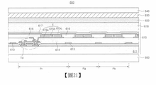
圖21是說明根據本發明一實施例之顯示裝置的示例的示意圖。舉例來說,顯示裝置600使用有機發光顯示面板。 21 is a schematic diagram illustrating an example of a display device according to an embodiment of the present invention. For example, the
參考圖21,顯示裝置600可以包括:散熱膜650、在散熱膜650上的有機發光二極體(OLED)顯示面板610、在OLED顯示面板610上的光路徑調整膜620、在光路徑調整膜620上的偏光板630、以及在偏光板630上並保護OLED顯示面板610的保護玻璃640。上述實施例的光路徑調整膜的其中之一被用作光路徑調整膜620。 Referring to FIG. 21, the
散熱膜650作用為防止在操作OLED顯示面板610時產生的熱量以及由於驅動薄膜電晶體Td的劣化而導致的壽命的迅速降低。散熱膜650可被配置為具有連續的不均勻形狀,以增加與環境空氣接觸的表面積。 The
OLED顯示面板610可以包括:包含複數個子像素Pr、Pg、和Pb的第一基板611、形成在各個子像素Pr、Pg、和Pb處的複數個有機發光二極體E、以及覆蓋有機發光二極體E的封裝層618。 The
驅動薄膜電晶體Td形成在第一基板611的內表面上的每一個子像素中,並且第一鈍化層614形成在驅動薄膜電晶體Td上。 The driving thin film transistor Td is formed in each sub-pixel on the inner surface of the
驅動薄膜電晶體Td包含:半導體層、閘極電極、源極電極、和汲極電極。在閘極電極上形成層間絕緣層,並且在層間絕緣層上形成資料線613。 The driving thin film transistor Td includes: a semiconductor layer, a gate electrode, a source electrode, and a drain electrode. An interlayer insulating layer is formed on the gate electrode, and a
第一電極615a形成在每一個子像素中的第一鈍化層614上並連接到驅動薄膜電晶體Td。在各個子像素Pr、Pg、和Pb中形成發射紅(R)光、綠(G)光、和藍(B)光的有機發光層615b。第二電極615c完全形成在有機發光層615b上。 The
堤岸層616形成在第一電極615a上。堤岸層616用於將發射紅(R)、綠(G)光、和藍(B)光的有機發光層615b分離成各個子像素Pr、Pg、和Pb。 The
每一個子像素中的第一電極615a、有機發光層615b、和第二電極165c構成有機發光二極體E。 The
第二鈍化層617形成在第二電極615c上,封裝層618形成在第二鈍化層617上。 The
封裝層618可以在第二鈍化層617上使用有機層及/或無機層形成多層結構,或者可以在第二鈍化層617上形成面密封。 The
第一基板611可以被稱為下基板、TFT基板、或背板,並且可以由玻璃或塑料製成。 The
第二鈍化層617作用為防止濕氣或外來物質從外部滲透。封裝層618作用為防止濕氣或外來物質從外部滲透,並吸收外部衝擊。舉例來說,OLED顯示面板610的上述結構可以具有其他結構。 The
可以在OLED顯示面板610上塗覆黏合劑材料,並且光路徑調整膜620可以貼附到OLED顯示面板。因此,由OLED顯示面板610產生的光的路徑擴大到對應於非開口區域(例如,圖15的411b)的區域,從而可以保持清晰的影像,並且格子狀圖案可以減少。 An adhesive material may be coated on the
OLED顯示面板610受光路徑調整膜620保護,而且可以進一步地提高OLED顯示面板610的可靠性。 The
偏光板630防止由OLED顯示面板610產生的光和進入OLED顯示面板610並被OLED顯示面板610中的反射材料反射的外部光引起相互干涉和顯示性能下降。在作為反射防止濾光器的偏光板630中,偏光板的吸收軸和延遲膜的光軸(例如吸收軸)被離軸佈置以使被OLED顯示面板610中的反射材料反射的外部光旋轉。 The
作為示例,描述位於OLED顯示面板610與偏光板630之間的光路徑調整膜620。光路徑調整膜620可以位於例如偏光板630上的其他位置。 As an example, the light
當顯示裝置600應用於VR裝置時,由於VR裝置的結構,可以省略保護玻璃640和偏光板630。 When the
圖22是說明根據本發明一實施例之顯示裝置的示例的示意圖。舉例來說,顯示裝置使用液晶顯示面板。 22 is a schematic diagram illustrating an example of a display device according to an embodiment of the present invention. For example, the display device uses a liquid crystal display panel.
參考圖22,顯示裝置700可以包括液晶顯示面板710、以及在液晶顯示面板710上的光路徑調整膜720。上述實施例的光路徑調整膜的其中之一被用作為光路徑調整膜720。 Referring to FIG. 22, the
液晶顯示面板710可以包含:第一基板711、第二基板712、和在第一基板711與第二基板712之間的液晶層779。 The liquid crystal display panel 710 may include a
在第一基板711上形成沿著一個方向的複數條閘極線。複數條共同線形成在第一基板上,並且與相應的閘極線隔開並平行。 A plurality of gate lines along one direction are formed on the
作為開關元件的薄膜電晶體Tr形成在開關區域TrA中,並且包含:彼此隔開的閘極電極713、閘極絕緣層714、半導體層715、以及源極電極716和汲極電極717。 A thin film transistor Tr as a switching element is formed in the switching region TrA, and includes: a
複數條資料線780形成在閘極絕緣層714上並且與複數條閘極線交叉以界定複數個子像素Pa。資料線780連接到源極電極716。 A plurality of
在薄膜電晶體Tr和資料線780上形成由例如無機絕緣材料製成的第一鈍化層718,並且在第一鈍化層718上形成由例如有機絕緣材料製成的第二鈍化層719,鈍化層718並具有平坦的頂表面。第一鈍化層718和第二鈍化層719具有暴露汲極電極717的汲極接觸孔719a和暴露共同線的共同接觸孔。 A
複數個像素電極770和複數個共同電極771形成在每一個子像素Pa中的第二鈍化層719上,並交替地佈置在子像素Pa中。像素電極770和共同電極771中的每一個由透明導電材料製成,例如ITO或IZO。像素電極770通過汲極接觸孔719a連接到汲極電極717,共同電極771通過共同接觸孔連接到共同線。 A plurality of
黑色矩陣772形成在第二基板712的內表面上,並且對應於每一個子像素的邊界部分和薄膜電晶體Tr。在第二基板712上形成彩色濾光片層773,其包含與各個子像素對應的紅色(R)、綠色(G)、和藍色(B)彩色濾光片圖案。彩色濾光片圖案的邊緣部分可以重疊黑色矩陣772。 The
覆蓋層778形成在彩色濾光片層773上,並具有平坦的表面。 The
第一偏光板781和第二偏光板782位於第一基板711和第二基板712的外表面上。第一偏光板781和第二偏光板782中的每一個透射具有平行於每一個第一偏光板781和第二偏光板782的透射軸的偏光方向的光。第一偏光板781和第二偏光板782的透射軸的佈置以及液晶分子的排列決定了光透射。例如,第一偏光板781和第二偏光板782的透射軸彼此垂直。 The first
光路徑調整膜720可以貼附在第二偏光板782的外表面上。或者,光路徑調整膜720可以在第二基板712與第二偏光板782之間插入。因此,光路徑調整膜720將由液晶顯示面板710產生的光的路徑擴大到與非開口區域(例如,圖15的411b)對應的區域,從而可以保持清晰的影像並且減少格子狀圖案可以實現。 The light
在本實施方式中,以液晶顯示面板為例進行說明,但也可以使用其他種類的顯示面板。 In this embodiment, a liquid crystal display panel is used as an example for description, but other types of display panels may be used.
此外,在上述實施例中,PenTile結構以示例的方式被描述,並且可以使用其他結構。 Furthermore, in the above-described embodiments, the PenTile structure is described by way of example, and other structures may be used.
以上所述者僅為用以解釋本發明之較佳實施例,並非企圖據以對本發明做任何形式上之限制,是以,凡有在相同之發明精神下所作有關本發明之任何修飾或變更,皆仍應包括在本發明意圖保護之範疇。 The above are only for explaining the preferred embodiments of the present invention, and are not intended to limit the present invention in any form, so that any modifications or changes made to the present invention under the same spirit of the invention , Should still be included in the scope of protection of the present invention.
本申請案主張2016年12月14日提出之韓國專利申請第10-2016-0170725號的優先權權益,上述韓國專利申請併入於此作為參考,如完整記載於本申請中。 This application claims the priority right of Korean Patent Application No. 10-2016-0170725 filed on December 14, 2016. The above Korean patent application is incorporated herein by reference, and is fully described in this application as if it were complete.
100‧‧‧顯示裝置 100‧‧‧Display device
110‧‧‧顯示面板 110‧‧‧Display panel
120‧‧‧光路徑調整膜 120‧‧‧Light path adjustment film
121‧‧‧第一基底膜 121‧‧‧The first basement membrane
122‧‧‧圖案層 122‧‧‧pattern layer
123‧‧‧第二基底膜 123‧‧‧Second basement membrane
124‧‧‧圖案、第一圖案 124‧‧‧pattern, first pattern
125‧‧‧氣隙、第二圖案 125‧‧‧Air gap, second pattern
Claims (18)
Applications Claiming Priority (3)
| Application Number | Priority Date | Filing Date | Title |
|---|---|---|---|
| KR1020160170725A KR102723297B1 (en) | 2016-07-26 | 2016-12-14 | Display Device |
| ??10-2016-0170725 | 2016-12-14 | ||
| KR10-2016-0170725 | 2016-12-14 |
Publications (2)
| Publication Number | Publication Date |
|---|---|
| TW201834233A TW201834233A (en) | 2018-09-16 |
| TWI683432B true TWI683432B (en) | 2020-01-21 |
Family
ID=60582410
Family Applications (1)
| Application Number | Title | Priority Date | Filing Date |
|---|---|---|---|
| TW106140773A TWI683432B (en) | 2016-12-14 | 2017-11-23 | Display device |
Country Status (3)
| Country | Link |
|---|---|
| EP (1) | EP3336915B1 (en) |
| JP (1) | JP6612309B2 (en) |
| TW (1) | TWI683432B (en) |
Families Citing this family (4)
| Publication number | Priority date | Publication date | Assignee | Title |
|---|---|---|---|---|
| CN110767678B (en) * | 2018-08-06 | 2024-03-29 | 云谷(固安)科技有限公司 | Display panel, display screen and display terminal |
| KR102618812B1 (en) * | 2018-10-31 | 2023-12-28 | 삼성디스플레이 주식회사 | Foldable display device |
| JP7045655B2 (en) * | 2020-03-13 | 2022-04-01 | 大日本印刷株式会社 | Display device and optical film manufacturing method |
| US20230093069A1 (en) * | 2020-03-13 | 2023-03-23 | Dai Nippon Printing Co., Ltd. | Display device and method for manufacturing optical film |
Citations (4)
| Publication number | Priority date | Publication date | Assignee | Title |
|---|---|---|---|---|
| TWI238432B (en) * | 2002-12-17 | 2005-08-21 | Seiko Epson Corp | Self-emitting element, display panel, display apparatus, and method of manufacturing self-emitting element |
| US20100245738A1 (en) * | 2007-11-22 | 2010-09-30 | Sharp Kabushiki Kaisha | Liquid crystal display device |
| US20150042935A1 (en) * | 2012-03-28 | 2015-02-12 | Sharp Kabushiki Kaisha | Light control film, display device, and method for manufacturing light control film |
| TW201545885A (en) * | 2014-03-28 | 2015-12-16 | Tomoegawa Co Ltd | Anisotropic optical film |
Family Cites Families (16)
| Publication number | Priority date | Publication date | Assignee | Title |
|---|---|---|---|---|
| JP3573393B2 (en) * | 1996-12-27 | 2004-10-06 | パイオニア株式会社 | Display device |
| JP5027969B2 (en) * | 2001-08-27 | 2012-09-19 | 大日本印刷株式会社 | Manufacturing method of two-dimensional field expansion member |
| JP2003202415A (en) * | 2001-12-28 | 2003-07-18 | Clariant Internatl Ltd | Optical film with controlled scattering and transmission characteristic and liquid crystal display using the same |
| JP2003282260A (en) * | 2002-03-26 | 2003-10-03 | Dainippon Printing Co Ltd | Electroluminescence display device |
| JP3951893B2 (en) * | 2002-11-11 | 2007-08-01 | セイコーエプソン株式会社 | Display body, display panel and display device |
| JP2004199006A (en) * | 2002-12-20 | 2004-07-15 | Koninkl Philips Electronics Nv | Light converging substrate, display device using the same and its manufacturing method |
| JP2004241214A (en) * | 2003-02-05 | 2004-08-26 | Stanley Electric Co Ltd | EL element |
| JP2007248484A (en) * | 2006-03-13 | 2007-09-27 | Sony Corp | Display device |
| KR101830969B1 (en) * | 2007-10-16 | 2018-02-21 | 쓰리엠 이노베이티브 프로퍼티즈 컴파니 | Higher transmission light control film |
| KR101546554B1 (en) * | 2007-12-21 | 2015-08-25 | 쓰리엠 이노베이티브 프로퍼티즈 컴파니 | Light control film |
| JP5946236B2 (en) * | 2009-07-06 | 2016-07-06 | 大日本印刷株式会社 | Display device |
| US20120224355A1 (en) * | 2009-12-01 | 2012-09-06 | Yasuyuki Umenaka | Light diffusion sheet, display panel, and display device |
| WO2011162013A1 (en) * | 2010-06-23 | 2011-12-29 | シャープ株式会社 | Display device and production method thereof |
| JP2014106249A (en) * | 2012-11-22 | 2014-06-09 | Sharp Corp | Polarizer and method for manufacturing the same, and display device |
| JP6103377B2 (en) * | 2013-06-19 | 2017-03-29 | シャープ株式会社 | Display device and manufacturing method thereof |
| KR102281937B1 (en) * | 2014-12-29 | 2021-07-28 | 삼성디스플레이 주식회사 | Display device |
-
2017
- 2017-11-23 TW TW106140773A patent/TWI683432B/en active
- 2017-11-29 EP EP17204432.3A patent/EP3336915B1/en active Active
- 2017-12-08 JP JP2017236075A patent/JP6612309B2/en active Active
Patent Citations (4)
| Publication number | Priority date | Publication date | Assignee | Title |
|---|---|---|---|---|
| TWI238432B (en) * | 2002-12-17 | 2005-08-21 | Seiko Epson Corp | Self-emitting element, display panel, display apparatus, and method of manufacturing self-emitting element |
| US20100245738A1 (en) * | 2007-11-22 | 2010-09-30 | Sharp Kabushiki Kaisha | Liquid crystal display device |
| US20150042935A1 (en) * | 2012-03-28 | 2015-02-12 | Sharp Kabushiki Kaisha | Light control film, display device, and method for manufacturing light control film |
| TW201545885A (en) * | 2014-03-28 | 2015-12-16 | Tomoegawa Co Ltd | Anisotropic optical film |
Also Published As
| Publication number | Publication date |
|---|---|
| JP6612309B2 (en) | 2019-11-27 |
| TW201834233A (en) | 2018-09-16 |
| JP2018097365A (en) | 2018-06-21 |
| EP3336915B1 (en) | 2024-11-27 |
| EP3336915A1 (en) | 2018-06-20 |
Similar Documents
| Publication | Publication Date | Title |
|---|---|---|
| US10983388B2 (en) | Display device | |
| US10732449B2 (en) | Display device | |
| US10211424B2 (en) | Multi-vision display apparatus including flexible display panel | |
| US10802347B2 (en) | Display device and color filter substrate | |
| TWI683432B (en) | Display device | |
| JP2008242307A (en) | Liquid crystal display panel with microlens array | |
| JP2014032346A (en) | Liquid crystal display panel | |
| US10197842B2 (en) | Liquid crystal display device | |
| WO2018116514A1 (en) | Multi-display | |
| WO2020129343A1 (en) | Electronic device with integrated camera and display device | |
| US20100085508A1 (en) | Display panel and liquid crystal display having the same | |
| KR102218049B1 (en) | Display device | |
| KR102313367B1 (en) | organic light emitting display apparatus | |
| KR102469498B1 (en) | Display Device | |
| US10228585B2 (en) | Color filter substrate and liquid crystal display | |
| CN106990603B (en) | Display panel and display device using same | |
| US20190129240A1 (en) | Display panel and display apparatus using the same | |
| KR102326302B1 (en) | Display Device | |
| JP6794225B2 (en) | Liquid crystal device | |
| KR101893939B1 (en) | Contact structure of line and LCD including the same | |
| JP6289782B1 (en) | Multi display | |
| JP2017116658A (en) | Liquid crystal display | |
| WO2020035989A1 (en) | Display device | |
| JP2016071148A (en) | Liquid crystal display device | |
| JP2009244409A (en) | Display panel |