TW202100975A - Fluid feed hole corrosion detection - Google Patents
Fluid feed hole corrosion detection Download PDFInfo
- Publication number
- TW202100975A TW202100975A TW109104522A TW109104522A TW202100975A TW 202100975 A TW202100975 A TW 202100975A TW 109104522 A TW109104522 A TW 109104522A TW 109104522 A TW109104522 A TW 109104522A TW 202100975 A TW202100975 A TW 202100975A
- Authority
- TW
- Taiwan
- Prior art keywords
- fluid
- corrosion detection
- conduction path
- corrosion
- detection conduction
- Prior art date
Links
Images


Classifications
-
- B—PERFORMING OPERATIONS; TRANSPORTING
- B41—PRINTING; LINING MACHINES; TYPEWRITERS; STAMPS
- B41J—TYPEWRITERS; SELECTIVE PRINTING MECHANISMS, i.e. MECHANISMS PRINTING OTHERWISE THAN FROM A FORME; CORRECTION OF TYPOGRAPHICAL ERRORS
- B41J2/00—Typewriters or selective printing mechanisms characterised by the printing or marking process for which they are designed
- B41J2/005—Typewriters or selective printing mechanisms characterised by the printing or marking process for which they are designed characterised by bringing liquid or particles selectively into contact with a printing material
- B41J2/01—Ink jet
- B41J2/135—Nozzles
- B41J2/14—Structure thereof only for on-demand ink jet heads
- B41J2/14016—Structure of bubble jet print heads
- B41J2/14153—Structures including a sensor
-
- B—PERFORMING OPERATIONS; TRANSPORTING
- B41—PRINTING; LINING MACHINES; TYPEWRITERS; STAMPS
- B41J—TYPEWRITERS; SELECTIVE PRINTING MECHANISMS, i.e. MECHANISMS PRINTING OTHERWISE THAN FROM A FORME; CORRECTION OF TYPOGRAPHICAL ERRORS
- B41J2/00—Typewriters or selective printing mechanisms characterised by the printing or marking process for which they are designed
- B41J2/005—Typewriters or selective printing mechanisms characterised by the printing or marking process for which they are designed characterised by bringing liquid or particles selectively into contact with a printing material
- B41J2/01—Ink jet
- B41J2/17—Ink jet characterised by ink handling
- B41J2/175—Ink supply systems ; Circuit parts therefor
-
- G—PHYSICS
- G01—MEASURING; TESTING
- G01N—INVESTIGATING OR ANALYSING MATERIALS BY DETERMINING THEIR CHEMICAL OR PHYSICAL PROPERTIES
- G01N17/00—Investigating resistance of materials to the weather, to corrosion, or to light
-
- G—PHYSICS
- G01—MEASURING; TESTING
- G01N—INVESTIGATING OR ANALYSING MATERIALS BY DETERMINING THEIR CHEMICAL OR PHYSICAL PROPERTIES
- G01N17/00—Investigating resistance of materials to the weather, to corrosion, or to light
- G01N17/008—Monitoring fouling
Landscapes
- Life Sciences & Earth Sciences (AREA)
- Analytical Chemistry (AREA)
- General Health & Medical Sciences (AREA)
- Environmental & Geological Engineering (AREA)
- Environmental Sciences (AREA)
- Physics & Mathematics (AREA)
- Health & Medical Sciences (AREA)
- Ecology (AREA)
- Chemical & Material Sciences (AREA)
- Biochemistry (AREA)
- Biodiversity & Conservation Biology (AREA)
- General Physics & Mathematics (AREA)
- Immunology (AREA)
- Pathology (AREA)
- Micromachines (AREA)
- Particle Formation And Scattering Control In Inkjet Printers (AREA)
- Investigating Or Analyzing Materials By The Use Of Electric Means (AREA)
Abstract
Description
發明領域Invention field
本發明係有關於流體進送孔腐蝕檢測技術The present invention relates to corrosion detection technology for fluid feeding holes
發明背景Background of the invention
例如噴墨列印機的許多流體噴射裝置包括流體耦接流體貯器與複數個流體噴射致動器、噴嘴及/或流體泵(統稱為「流體噴射元件」)的流體進送「槽」。這有效地建立流體進送槽與多個流體噴射元件之間的一對多關係。不過,有些較新的流體噴射裝置包括流體耦接流體貯器與複數個流體噴射元件的複數個流體進送「孔」。流體進送孔傾向遠小於流體進送槽,使得難以沉積保護材料於流體進送孔上,或在流體進送孔四周提供保護邊限。結果,流體進送孔比流體進送槽更容易受影響於由流體造成的腐蝕或「過度蝕刻」。For example, many fluid ejection devices of inkjet printers include fluid feed "tanks" that are fluidly coupled to a fluid reservoir and a plurality of fluid ejection actuators, nozzles, and/or fluid pumps (collectively referred to as "fluid ejection elements"). This effectively establishes a one-to-many relationship between the fluid feed slot and the plurality of fluid ejection elements. However, some newer fluid ejection devices include a plurality of fluid feed "holes" that fluidly couple a fluid reservoir and a plurality of fluid ejection elements. The tendency of the fluid feed hole is much smaller than that of the fluid feed groove, making it difficult to deposit protective material on the fluid feed hole or provide a protective margin around the fluid feed hole. As a result, the fluid feed hole is more susceptible to corrosion or "over etching" caused by the fluid than the fluid feed groove.
發明概要Summary of the invention
依據本發明之一實施例,係特地提出一種流體噴射裝置,其包含:包括一流體進送孔的一基板;以及一腐蝕檢測傳導路徑,其設置在該流體進送孔的一壁部後面;其中,該腐蝕檢測傳導路徑是用以響應於該腐蝕檢測傳導路徑對一流體之暴露而閉合一電路。According to an embodiment of the present invention, a fluid ejection device is specially proposed, which includes: a substrate including a fluid feed hole; and a corrosion detection conduction path, which is arranged behind a wall of the fluid feed hole; Wherein, the corrosion detection conduction path is used to close a circuit in response to the exposure of the corrosion detection conduction path to a fluid.
為了簡化及圖解說明的目的,本揭示內容主要以參考彼之實施例來描述。在以下描述中,為了提供本揭示內容的徹底了解,提出許多特定細節。不過,應瞭解,可實施本揭示內容而不受限於該等特定細節。在其他情況下,有些方法及結構不予詳述以免不必要地混淆本揭示內容。For the purpose of simplification and illustration, the present disclosure is mainly described with reference to other embodiments. In the following description, in order to provide a thorough understanding of the present disclosure, many specific details are proposed. However, it should be understood that the present disclosure can be implemented without being limited to these specific details. In other cases, some methods and structures are not described in detail so as not to unnecessarily confuse the present disclosure.
另外,應瞭解,描繪於附圖中的元件可能包括額外的組件且可移除及/或修改描述於附圖中的組件中之一些而不脫離揭露於本文之元件的範疇。也應瞭解,描繪於附圖中的元件可能不按比例繪製,且因此,該等元件可能與圖中的有不同的尺寸及/或組態。In addition, it should be understood that the elements depicted in the drawings may include additional components and some of the components described in the drawings may be removed and/or modified without departing from the scope of the elements disclosed herein. It should also be understood that the elements depicted in the drawings may not be drawn to scale, and therefore, the elements may have different sizes and/or configurations from those in the drawings.
描述於本文的技術、設備及系統係用於監控及/或檢測製造流體進送孔於其中之材料的腐蝕或「過度蝕刻」。描述於本文的實施例例如可與使用於二維及/或三維列印之噴墨列印頭及/或列印頭晶粒一起實施。例如,採用傳導路徑之形式的感測器可設置在流體進送孔的壁部後面以檢測過度蝕刻。此一傳導路徑可採用各種形式,例如二極體、電阻器、導體、或埋藏植入層。在流體進送孔(s)被流體蝕刻或腐蝕時,傳導路徑最終會暴露於流體(例如,墨水)。在一些實施例中,這在傳導路徑與流體之間建立有效地閉合電路的電耦合。使用各種類型的邏輯及/或感測電路可檢測此電路的閉合。在一些實施例中,傳導路徑可形成為植入層,相較於例如沉積薄膜層,這允許增加植入深度(導致與墨水的接觸增加)及導電率。不過,在某些情況下,傳導路徑也可使用沉積薄膜層。The techniques, equipment, and systems described herein are used to monitor and/or detect corrosion or "over-etching" of materials in which fluid feed holes are made. The embodiments described herein can be implemented, for example, with inkjet print heads and/or print head dies used in 2D and/or 3D printing. For example, a sensor in the form of a conductive path can be placed behind the wall of the fluid feed hole to detect over-etching. This conductive path can take various forms, such as a diode, a resistor, a conductor, or a buried implant layer. When the fluid feed hole(s) is etched or corroded by the fluid, the conductive path will eventually be exposed to the fluid (for example, ink). In some embodiments, this establishes an electrical coupling between the conductive path and the fluid that effectively closes the circuit. Various types of logic and/or sensing circuits can be used to detect the closure of this circuit. In some embodiments, the conductive path may be formed as an implanted layer, which allows for increased implantation depth (resulting in increased contact with ink) and conductivity compared to, for example, a deposited thin film layer. However, in some cases, the conductive path can also use deposited thin film layers.
本文考慮到用於傳導路徑之結構的許多實施例。在一實施例中,傳導路徑電性耦接至設置於例如矽流體噴射晶粒之流體晶粒上的類比至數位轉換器(「A/D」)。在一些此類實施例中,由傳導路徑產生的「過度蝕刻狀態」訊號可在晶粒上數位化然後傳達至晶粒外邏輯(參考圖10A),例如列印系統的感測電路。在一些實施例中,晶粒上A/D可能已經存在於晶粒上,例如,用於熱控制或其他感測功能,且可改變以用於過度蝕刻檢測,如本文所述。在其他情況下,由傳導路徑之暴露而產生的類比訊號可路由到晶粒外,例如,經由耦接至外部感測電路(參考圖10B)的接合墊或電連接。This article considers many embodiments for the structure of the conductive path. In one embodiment, the conductive path is electrically coupled to an analog-to-digital converter ("A/D") disposed on a fluid die, such as a silicon fluid jet die. In some such embodiments, the "over-etch state" signal generated by the conductive path can be digitized on the die and then transmitted to the off-die logic (refer to FIG. 10A), such as the sensing circuit of the printing system. In some embodiments, on-die A/D may already exist on the die, for example, for thermal control or other sensing functions, and can be changed for over-etch detection, as described herein. In other cases, the analog signal generated by the exposure of the conductive path can be routed to the outside of the die, for example, via a bonding pad or electrical connection coupled to an external sensing circuit (refer to FIG. 10B).
如本文所使用的,用語「蝕刻(etch)」或「蝕刻(etching)」用來指例如矽之基板的劣化或腐蝕,這是由於基板長期暴露於例如墨水的流體造成。此外,如本文所使用的,用語「過度蝕刻(over-etch)」或「過度蝕刻」用來指基板的超前劣化或腐蝕,這可能影響基板的結構完整性或功能能力到可能需要干預的程度。As used herein, the term "etch" or "etching" is used to refer to the deterioration or corrosion of a substrate such as silicon, which is caused by long-term exposure of the substrate to fluids such as ink. In addition, as used herein, the terms "over-etch" or "over-etch" are used to refer to advanced degradation or corrosion of the substrate, which may affect the structural integrity or functional capabilities of the substrate to the extent that intervention may be required .
圖1的方塊圖圖示噴墨列印系統100的實施例,它使用噴墨列印頭可用來形成圖像。噴墨列印系統100包括含有許多列印頭104的列印條102,與墨水供給總成106。墨水供給總成106包括墨水貯器108。提供來自墨水貯器108的墨水110給列印條102以進送到列印頭104。墨水供給總成106與列印條102可使用單向墨水輸送系統或循環墨水輸送系統。在單向墨水輸送系統中,在列印期間實質消耗所有供給至列印條102的墨水。在循環墨水輸送系統中,在列印期間消耗供給至列印條102的墨水110之一部份,且使墨水的另一部份回到墨水供給總成。在一實施例中,墨水供給總成106與列印條102分離,且通過例如供給管(未圖示)的管狀連接件供給墨水110至列印條102。在其他實施例中,例如,在單一使用者列印機中,列印條102可包括墨水供給總成106,與墨水貯器108,以及列印頭104。在任一實施例中,可卸下及更換或再裝滿墨水供給總成106的墨水貯器108。The block diagram of FIG. 1 illustrates an embodiment of an
來自列印頭104的墨水110從噴嘴朝向例如紙、邁勒膠片(Mylar)、卡片紙及其類似者的印刷媒體114噴出成為墨滴112。列印頭104的噴嘴排列成直行或陣列致使在列印條102與印刷媒體114彼此相對移動時,墨水110的正確定序噴射可形成要列印於印刷媒體114上的字元、符號、圖形、或其他圖像。墨水110不限於用來形成可見圖像於印刷媒體上的有色液體,例如,墨水110可為用來列印電路圖案的電活性物質,例如太陽能電池。The
安裝結構或總成116可用來使列印條102相對於印刷媒體114定位。在一實施例中,安裝總成116可處於使許多列印頭104保持在印刷媒體114上方的固定位置。在另一實施例中,例如,如果列印條102包括1到4個列印頭104,安裝總成116可包括使列印條102來回移動越過印刷媒體114的馬達。媒體傳輸總成118使印刷媒體114相對於列印條移動,例如,使印刷媒體114與列印條102垂直地移動。在一些實施例中,媒體傳輸總成118可包括數個輥,包括用來拉扯印刷媒體通過列印系統的任意多個電動夾送輥(motorized pinch roll)。如果列印條102移動,媒體傳輸總成118可使印刷媒體114與新位置相關連。在列印條102不移動的實施例中,印刷媒體114的運動可為連續式。The mounting structure or
控制器120接收來自例如電腦的主機系統122的資料。傳送該資料可透過可為電連接、光纖連接、或無線連接等等的網路連接124。透過網路連接124傳送的資料可包括待列印的文件或檔案,或可包括更多基本項目,例如文件的彩色平面或點陣化文件。控制器120可暫時儲存資料於用以分析的區域記憶體中。分析可包括判定用於從列印頭104噴出墨滴的時序控制,以及印刷媒體114的運動和列印條102的任何運動。控制器120透過控制線126可運作列印系統的個別部件。因此,控制器120界定由形成字元、符號、圖形、或其他圖像於印刷媒體114上之噴出墨滴112組成的圖案。The controller 120 receives data from a
噴墨列印系統100不限於圖示於圖1的元件。例如,控制器120可為耦接於對於系統之個別部件有獨立運算控制之網路中的叢集運算系統。例如,獨立控制器可與安裝總成116、列印條102、墨水供給總成106、和媒體傳輸總成118中之各者相關聯。在此實施例中,控制線126可為把獨立控制器耦接成單一網路的網路連接。在其他實施例中,例如,如果不需要由列印條102來移動它,安裝總成116可以不是與列印條102分離的元件。The
圖2圖示例如列印條102中處於示範印刷組態的噴墨列印頭104叢集。與圖1相同的元件用相同的元件符號表示。可使用處於列印頭不動之組態的圖2列印條102。因此,列印頭104可以重疊的組態附接至列印條102以提供完整的覆蓋。各個列印頭104具有使噴嘴及電路可用來噴射墨滴的多個噴嘴區域202。在有些情形下,噴嘴區域202可採用如本文所述之矽基流體晶粒的形式。FIG. 2 illustrates a cluster of inkjet print heads 104 in an exemplary printing configuration in, for example, the
圖3A至圖3B描繪形成於基板中的流體進送孔302,該基板可對應至例如在說明前面附圖時提及的噴嘴區域202或流體晶粒。在某些情況下,此基板可為矽基流體晶粒。如前述,流體進送孔302可小於流體進送槽,因此可能更容易受影響於由流體304造成的過度蝕刻(參考圖3B)。因此,例如腐蝕檢測傳導路徑306的感測器可設置於流體進送孔302的壁部320後面,致使,在腐蝕檢測傳導路徑306暴露於流體304時,閉合電路。在某些情況下,腐蝕檢測傳導路徑306可包括形成基板之矽的植入層。在某些情況下,該植入層有最大植入深度是可取的,這可導致可接觸更多的流體(蝕刻時)從而增加導電率。在其他情況下,腐蝕檢測傳導路徑306可包括沉積於基板中的薄膜層(例如,金屬)。FIGS. 3A to 3B depict a
如圖3A至圖3B所示,腐蝕檢測傳導路徑306可包括兩個電隔離部份308、310。電隔離部份308中之第一者經由元件312可耦接至電壓源。在某些情況下,該電壓源可為設置於晶粒上或者是晶粒外的電路316(參考圖10A至圖10B)。電隔離部份310中之第二者可耦接至接地314。這兩個電隔離部份308、310可經配置成便於響應於流體進送孔302之壁部320的腐蝕或蝕刻而經由該流體304耦接(參考圖3B)。在某些情況下,基板的各個平面的腐蝕或蝕刻可能以不均勻的速率發生。結果,圓形的流體進送孔302(如本文所示)可能腐蝕或蝕刻變成矩形(參考圖3B)。一旦流體進送孔腐蝕或蝕刻使得兩個電隔離部份308、310經由流體304電接觸,則可閉合包括腐蝕檢測傳導路徑306的電路。As shown in FIGS. 3A to 3B, the corrosion
在一些實施例中,電路316可施加電壓至腐蝕檢測傳導路徑306的第一電隔離部份308。在某些情況下,此電路316也可接收返回電流或測量所產生的電流。例如,返回電流可響應於腐蝕檢測傳導路徑306暴露於在流體進送孔302中的流體304來指示電路已閉合。此外,在某些情況下,此電路316也可運作地耦接至為了施加電壓而與電路316互動的控制器(1090,圖10)。In some embodiments, the circuit 316 can apply a voltage to the first electrically
在某些情況下,如圖4A至圖4B所示,可能沒有耦接至接地的獨立電隔離部份,如圖3A至圖3B所示。在此類實例中,腐蝕檢測傳導路徑406可包括可經由元件412耦接至例如電路416之電壓源的一電隔離部份408。在此類實例中,流體404本身(例如,墨水)可接地,且因此用作接地。在此一實例中,如圖4B所示,即使流體進送孔402的蝕刻不對稱,仍允許閉合與腐蝕檢測傳導路徑406一起形成的電路。In some cases, as shown in FIGS. 4A to 4B, there may not be an independent electrically isolated part coupled to the ground, as shown in FIGS. 3A to 3B. In such instances, the corrosion detection
可能有以下情況:流體晶粒包含流體進送孔的區域可能很擁擠而且在說明圖3A至圖3B及圖4A至B時提及用於腐蝕檢測傳導路徑的附加電路可能更難以實現。在此類實例中,如圖5所示,可使用代表性或「代理」流體進送孔502。在某些情況下,代表性流體進送孔502可能放在流體晶粒530落在由功能流體進送孔5201-n
組成之陣列外的區域上,但是仍然與流體504接觸。不過,在其他情況下,代表性流體進送孔502可在功能流體進送孔5201-n
的陣列中。不論代表性流體進送孔502如何安置,對應腐蝕檢測傳導路徑506及相關聯電路516可用作診斷流體進送孔,這允許在沒有緊鄰各個功能流體進送孔520的附加電路下檢測過度蝕刻。There may be the following situations: the area of the fluid crystal grain containing the fluid feed hole may be crowded and it may be more difficult to implement the additional circuit for the corrosion detection conduction path mentioned in the description of FIGS. 3A to 3B and 4A to B. In such instances, as shown in Figure 5, representative or "agent" fluid feed holes 502 may be used. In some cases, the representative
在某些情況下,例如如圖6至圖8所示,在流體晶粒上可能有複數個流體進送孔6021-n
、7021-n
、8021-n
。在圖6的實施例中,例如,複數個流體進送孔6021-n
包括設置在各個流體進送孔6021-n
之壁部6201-n
後面的對應腐蝕檢測傳導路徑6061-n
。複數個流體進送孔6021-n
也包括對應複數個可個別定址開關6101-n
,彼等可採用P型金屬氧化物半導體(「PMOS」)或N型金屬氧化物半導體(「NMOS」)場效電晶體(「FET」)的形式。各個可個別定址開關610可運作地耦接至對應腐蝕檢測傳導路徑606以及最終至電路616。In some cases, for example, as shown in FIGS. 6 to 8, there may be a plurality of fluid feed holes 602 1-n , 702 1-n , and 802 1-n on the fluid crystal grains. In the embodiment of FIG. 6, for example, a plurality of fluid feed supply opening 602 1-n includes a corresponding corrosion detection conducting path behind 620 1-n is provided in each fluid feed supply opening 602 1-n of the
作為一非限定性實施例,可個別定址開關6101-n
的控制可包括測試模式,在此可選擇可個別定址開關6101-n
以藉由判定包括對應腐蝕檢測傳導路徑606的電路是否閉合來進行過度蝕刻分析。這致能測試個別流體進送孔602的過度蝕刻,而且也允許平行測試或分析一個以上的流體進送孔6021-n
的過度蝕刻。此外,在某些情況下,由於開關6101-n
可個別定址,因此可判定任何被檢測過度蝕刻的區域或位置,這可能對診斷有用。例如,控制器(1090,圖10)通過電路616可傳送與該流體進送孔相關聯的一地址6024
,使得地址可用來區分流體進送孔6024
與在流體晶粒上的其他流體進送孔(例如,流體進送孔6021-3
)。As a non-limiting example, the control of the individually
與前面的實施例類似,在某些情況下,電路616可位在晶粒上(大體參考圖10A)上;同時在其他實例中,電路616可位於晶粒外且通過電連接接觸墊測量(大體參考圖10B)。在此類實例中,電連接接觸1075可使用於多個目的,包括但不限於:建立開關6101-n
的網路以使晶粒上的開關多路傳輸至電連接接觸1075。Similar to the previous embodiment, in some cases, the circuit 616 can be located on the die (generally refer to FIG. 10A); while in other cases, the circuit 616 can be located outside the die and measured by electrical connection contact pads ( Refer generally to Figure 10B). In such instances, the electrical connection contacts 1075 can be used for multiple purposes, including but not limited to: establishing a network of
在其他實施例中,個別流體進送孔可能無法個別分析。特別參考圖7,複數個流體進送孔7021-n
包括設置在流體進送孔7021-n
之壁部7081-n
後面的對應複數個腐蝕檢測傳導路徑7061-n
。不過,在圖7中,腐蝕檢測傳導路徑6061-4
互相實體或「電流(galvanic)」接觸,而不是如圖6所示呈空間分離。例如,第一流體進送孔7021
的第一腐蝕檢測傳導路徑7061
與緊鄰流體進送孔(例如,第二流體進送孔7022
)的第二腐蝕檢測傳導路徑7062
實體接觸。In other embodiments, individual fluid feed holes may not be individually analyzed. With particular reference to FIG. 7, a plurality of fluid feed holes feeding corresponding to 702 1-n is provided comprising 708 1-n back into the
在圖7中,由實體接觸腐蝕檢測傳導路徑7061-4
形成的陣列之一端連接至電路716。電路716可與前面的電路實例(例如,316、416、516、616)共享各種特性。在流體晶粒上有足夠空間的一些實施例中,可提供低阻抗連線7201-n
(虛線)以連接個別腐蝕檢測傳導路徑706至陣列的其他位置。腐蝕檢測傳導路徑706與鄰近腐蝕檢測傳導路徑706的接觸可允許過度蝕刻的平行分析,這樣可同時分析所有流體進送孔7021-n
的過度蝕刻。結果,控制器(1090,圖10)能夠基於返回電流的量值來判定過度蝕刻流體進送孔(亦即,暴露於流體的腐蝕檢測傳導路徑)的個數(或計數)。例如,相較於返回電流較低的情形,較大的返回電流可指示較多個過度蝕刻的流體進送孔。此外,在平行分析多個流體進送孔7021-n
的過度蝕刻下,可能出現較大(更加可檢測)的過度蝕刻訊號,特別是在多個流體進送孔7021-n
已被過度蝕刻時。In FIG. 7, one end of the array formed by the physical contact corrosion detection
此時參考圖8,複數個流體進送孔8021-n
再一次包括設置在各個流體進送孔之壁部8081-n
後面的對應複數個腐蝕檢測傳導路徑8061-n
。不過,跟圖7不一樣,在圖8中,腐蝕檢測傳導路徑8061-n
彼此空間分離。如圖8所示,在某些情況下,低電阻互連層820可連接空間分離的腐蝕檢測傳導路徑8061-n
。在某些情況下,低電阻互連層820可為薄膜金屬。由於低電阻互連層820施加相對低的電阻,可以比在腐蝕檢測傳導路徑之間有較大電阻的其他實施例更容易地檢測流體進送孔8021-n
的過度蝕刻。且如同在圖7之實施例中的情形,在此實施例中,較大的返回電流可能指明較多個過度蝕刻的流體進送孔802。與前面的實施例一樣,電路816可與前面的實例共享各種特性,例如電路316、416、516、616、716。Referring now to FIG. 8, the plurality of
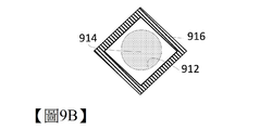
在前面的實施例中,腐蝕檢測傳導路徑主要被圖示成彼等係繞著流體進送孔的整個周邊同心延伸。不過,這沒有限定的意思。該腐蝕檢測傳導路徑可為能夠響應於暴露於包含在流體進送孔內之流體來閉合電路的任何形狀。圖9A至圖9C圖示有各種形狀的各種傳導路徑。圖9A圖示繞著流體進送孔902之整個周邊同心延伸的腐蝕檢測傳導路徑906。圖9B圖示以正方形形式繞著流體進送孔912之整個周邊延伸的腐蝕檢測傳導路徑916致使與流體進送孔912及腐蝕檢測傳導路徑916的距離有所不同。圖9C圖示以例如半圓的形式繞著流體進送孔922之整個周邊部份延伸的腐蝕檢測傳導路徑926。不論結構如何,當腐蝕檢測傳導路徑906、916、926暴露於流體進送孔902、912、922的流體904、914、924時,電路都會被閉合。In the previous embodiments, the corrosion detection conduction paths are mainly illustrated as they extend concentrically around the entire periphery of the fluid feed hole. However, this has no limiting meaning. The corrosion detection conductive path may be any shape capable of closing the circuit in response to exposure to the fluid contained in the fluid feed hole. 9A to 9C illustrate various conductive paths of various shapes. FIG. 9A illustrates a corrosion
如前述,連接至腐蝕檢測傳導路徑(s)的電路(例如,216、316、416、516、616、716、816)也可在流體晶粒1000上(圖10A)或在流體晶粒1055外(圖10B)。此時參考圖10A,該等流體進送孔可包含在流體晶粒1000的流體進送孔陣列1005區域中。流體進送孔陣列1005的感測節點1015可耦接至晶粒上類比至數位(A/D)轉換器1020。來自腐蝕檢測傳導路徑(s)的訊號可用A/D轉換器1020數位化以允許流體晶粒1000以數位方式傳遞過度蝕刻狀態至系統的控制器1090。在某些情況下,晶粒上A/D轉換器1020可能已經出現在流體晶粒上用於其他功能(亦即,熱控制或其他感測功能)且可改變以用於過度蝕刻檢測。As mentioned above, the circuit (for example, 216, 316, 416, 516, 616, 716, 816) connected to the corrosion detection conduction path (s) can also be on the fluid die 1000 (FIG. 10A) or outside the
類似圖示於圖10A的實施例,圖示於圖10B的實施例也可包括包含在流體晶粒1055之流體進送孔陣列1060區域內的數個流體進送孔。不過,圖示於圖10B的實施例包括晶粒外電路1080,在某些情況下,它可允許更先進的處理。流體進送孔陣列1060的感測節點1070可耦接至也習知為發射墊或感測墊的電連接接觸1075。此電連接接觸1075可耦接至為系統1050之一部份的外部晶粒外電路1080。在某些情況下,電連接接觸1075也可使用於其他感測功能。Similar to the embodiment shown in FIG. 10A, the embodiment shown in FIG. 10B may also include a plurality of fluid feeding holes included in the fluid feeding hole array 1060 region of the
不論該電路設置於流體晶粒上還是在流體晶粒外,該系統通過控制器1090可請求關於過度蝕刻的資訊。如果過度蝕刻被檢測,例如腐蝕檢測傳導路徑暴露於流體,流體晶粒1000、1055可有效地通知該系統需要干預(例如,更換列印頭)。Regardless of whether the circuit is provided on or outside the fluid die, the system can request information about over-etching through the
在某些情況下,如圖6所示,每個流體進送孔可包括可個別定址開關(例如,PMOS或NMOS FETs),彼等中之各者可運作地耦接至各個對應腐蝕檢測傳導路徑且最終至電路。在此類實例中,為了選擇監控過度蝕刻的感測器,流體晶粒1000、1055視需要可另外包括可控制可個別定址開關的感測器選擇控件1010、1065。In some cases, as shown in Figure 6, each fluid feed hole may include individually addressable switches (for example, PMOS or NMOS FETs), and each of them can be operatively coupled to each corresponding corrosion detection conduction Path and ultimately to the circuit. In such an example, in order to select a sensor for monitoring over-etching, the
圖11的流程圖根據本揭示內容圖示用於檢測流體噴射裝置之過度蝕刻的示範方法1100。應瞭解,在某些情況下,該方法可包括除圖示於圖11者以外的附加運作,可以不同的次序及/或平行執行圖11的運作,及/或可省略圖11的各種運作。The flowchart of FIG. 11 illustrates an
在區塊1105,可施加電壓至設置在流體進送孔之壁部後面的感測器。此電壓可允許檢測流體進送孔之壁部的腐蝕,因為在壁部被腐蝕或過度蝕刻時,感測器可與包含在流體進送孔內的流體接觸且形成電路,如前述。例如,通過與電路(在流體晶粒上或者是在其外)互動的控制器(例如,1090),可施加此電壓。該感測器可為在本文說明圖3至圖9時提及的腐蝕檢測傳導路徑實施例中之任一。In
在區塊1110,電流可響應於由於流體與感測器接觸而形成一電路而自感測器返回。在某些情況下,此電流的存在及/或量值可指示流體進送孔(s)的過度蝕刻狀態。At
儘管已具體描述本揭示內容的全部內容,然而本揭示內容的代表性實施例在範圍廣泛的應用有效用,且以上闡述非旨在且不應被視為限制,而是提供作為本揭示內容之方面的舉例說明。Although the entire content of the present disclosure has been described in detail, the representative embodiments of the present disclosure are effective in a wide range of applications, and the above description is not intended and should not be regarded as a limitation, but is provided as an example of the present disclosure Examples of aspects.
已描述及圖示於本文的是本揭示內容的一實施例及一些它的變體。使用於本文的用語、說明及圖表提出作為實例且無意作為限制。旨在由下列專利請求項及其等效陳述界定的本揭示內容範疇內可能有許多變體,其中以最廣泛的合理意思表示所有用語,除非另有明示。What has been described and illustrated herein is an embodiment of the present disclosure and some of its variations. The terms, descriptions and diagrams used in this article are presented as examples and are not intended to be limiting. There may be many variations within the scope of this disclosure, which are intended to be defined by the following patent claims and their equivalent statements, in which all terms are expressed in the broadest reasonable meaning, unless expressly stated otherwise.
100:噴墨列印系統 102:列印條 104:列印頭 106:墨水供給總成 108:(墨水)貯器 110:墨水 112:墨滴 114:印刷媒體 116:安裝結構或總成 118:媒體傳輸總成 120:電子控制器 122:主機系統 124:網路連接 126:控制線 202:噴嘴區域 216:電路 302:流體進送孔 304:流體 306:腐蝕檢測傳導路徑 308,310:電隔離部份 312:元件 314:接地 316:電路 320:壁部 402:流體進送孔 404:流體 406:腐蝕檢測傳導路徑 408:電隔離部份 412:元件 416:電路 502:代表性或「代理」流體進送孔 504:流體 506:腐蝕檢測傳導路徑 516:電路 5201-5206:功能流體進送孔 530:流體晶粒 6021-6024:個別流體進送孔 6061-6064:腐蝕檢測傳導路徑 6101-6104:可個別定址開關 616:電路 6201-6204:壁部 7021-7025:流體進送孔 7061-7065:個別腐蝕檢測傳導路徑 7081-7085:壁部 716:電路 7201-7205:低阻抗連線 8021-8025:流體進送孔 8061-8065:腐蝕檢測傳導路徑 8081-8085:壁部 816:電路 820:低電阻互連層 902:流體進送孔 904:流體 906:腐蝕檢測傳導路徑 912:流體進送孔 914:流體 916:腐蝕檢測傳導路徑 922:流體進送孔 924:流體 926:腐蝕檢測傳導路徑 1000:流體晶粒 1005:流體進送孔陣列 1010:視需要的感測器選擇控件 1015:感測節點 1020:晶粒上類比至數位(A/D)轉換器 1050:系統 1055:流體晶粒 1060:流體進送孔陣列 1065:視需要的感測器選擇控件 1070:感測節點 1075:電連接接觸 1080:(晶粒外)電路 1090:控制器 1100:示範方法 1105-1110:區塊100: Inkjet printing system 102: Printing strip 104: Print head 106: Ink supply assembly 108: (ink) reservoir 110: Ink 112: Ink drop 114: Printing media 116: Installation structure or assembly 118: Media transmission assembly 120: electronic controller 122: host system 124: network connection 126: control line 202: nozzle area 216: circuit 302: fluid feed hole 304: fluid 306: corrosion detection conduction path 308, 310: electrical isolation part 312: component 314: ground 316: circuit 320: wall 402: fluid feed hole 404: fluid 406: corrosion detection conduction path 408: electrical isolation part 412: component 416: circuit 502: representative or ``agent'' fluid inlet feeding hole 504: 506 fluids: corrosion Testing conductive path 516: 5201-5206 circuit: functional fluid feed inlet orifice 530: 6021-6024 fluid grain: an individual fluid feed supply opening 6061-6064: corrosion Testing conduction path 6101-6104: individually addressable switch 616: 6201-6204 circuit: 7021-7025 wall portions: a fluid feed inlet orifice 7061-7065: corrosion Testing of individual conductive paths 7081-7085: wall 716: 7201-7205 circuit: a low impedance connection 8021-8025: a fluid feed inlet orifice 8061-8065: corrosion Testing conductive paths 8081-8085: wall portion 816: circuit 820: a low resistance cross Connection layer 902: fluid feed hole 904: fluid 906: corrosion detection conduction path 912: fluid feed hole 914: fluid 916: corrosion detection conduction path 922: fluid feed hole 924: fluid 926: corrosion detection conduction path 1000: fluid Die 1005: fluid feed hole array 1010: optional sensor selection control 1015: sensing node 1020: analog to digital (A/D) converter on the die 1050: system 1055: fluid die 1060: fluid Feeding hole array 1065: optional sensor selection control 1070: sensing node 1075: electrical connection contact 1080: (outside the die) circuit 1090: controller 1100: demonstration method 1105-1110: block
本揭示內容的特徵以實施例舉例說明且不受限於以下附圖,其中類似的元件用相同的符號表示。The features of the present disclosure are illustrated by examples and are not limited to the following drawings, in which similar elements are represented by the same symbols.
圖1的方塊圖圖示使用流體噴射裝置可用來形成圖像的流體噴射系統實施例。The block diagram of FIG. 1 illustrates an embodiment of a fluid ejection system that can be used to form an image using a fluid ejection device.
圖2圖示由形式為噴墨列印頭之流體噴射裝置以例如列印條之示範印刷組態組成的叢集。Figure 2 illustrates a cluster composed of a fluid ejection device in the form of an inkjet print head in an exemplary printing configuration such as a print bar.
圖3A至圖3B舉例圖示可如何組裝根據本揭示內容之數個選定方面組配的流體噴射裝置。圖3A圖示傳導路徑,同時圖3B圖示使圖3A傳導路徑暴露於流體的蝕刻流體進送孔。Figures 3A to 3B illustrate how a fluid ejection device configured according to several selected aspects of the present disclosure can be assembled. FIG. 3A illustrates the conductive path, while FIG. 3B illustrates the etching fluid feeding hole exposing the conductive path of FIG. 3A to the fluid.
圖4A至圖4B另舉例圖示可如何組裝根據本揭示內容之數個選定方面組配的流體噴射裝置。圖4A圖示傳導路徑,同時圖4B圖示使圖4A傳導路徑暴露於流體的蝕刻流體進送孔。Figures 4A-4B further illustrate how a fluid ejection device configured according to several selected aspects of the present disclosure can be assembled. FIG. 4A illustrates the conductive path, while FIG. 4B illustrates the etching fluid feeding hole exposing the conductive path of FIG. 4A to the fluid.
圖5舉例圖示可如何組裝根據本揭示內容之數個選定方面組配具有代表性流體進送孔的流體噴射裝置。Figure 5 illustrates how a fluid ejection device with representative fluid feed holes can be assembled in accordance with several selected aspects of the present disclosure.
圖6舉例圖示可如何組裝根據本揭示內容之數個選定方面組配具有與傳導路徑可運作地耦接之可個別定址開關的流體噴射裝置。Figure 6 illustrates how a fluid ejection device with individually addressable switches operatively coupled to conductive paths can be assembled in accordance with several selected aspects of the present disclosure.
圖7舉例圖示可如何組裝根據本揭示內容之數個選定方面組配具有互相接觸之多個傳導路徑的流體噴射裝置。Figure 7 illustrates how a fluid ejection device with multiple conductive paths in contact with each other can be assembled in accordance with several selected aspects of the present disclosure.
圖8舉例圖示可如何組裝根據本揭示內容之數個選定方面組配具有在基板上空間分離且用低電阻互連層連接之多個傳導路徑的流體噴射裝置。Figure 8 illustrates how a fluid ejection device with multiple conductive paths spaced apart on a substrate and connected by low resistance interconnect layers can be assembled in accordance with several selected aspects of the present disclosure.
圖9A至圖9C圖示各種傳導路徑。圖9A圖示圓形的傳導路徑;圖9B圖示方形的傳導路徑;以及圖9C圖示部份包圍流體進送孔的傳導路徑。9A to 9C illustrate various conduction paths. 9A illustrates a circular conduction path; FIG. 9B illustrates a square conduction path; and FIG. 9C illustrates a conduction path that partially surrounds the fluid feeding hole.
圖10A至圖10B圖示示範流體晶粒。圖10A圖示有晶粒上電路的流體晶粒;圖10B圖示有晶粒外電路的流體晶粒。10A to 10B illustrate exemplary fluid crystal grains. FIG. 10A illustrates a fluid die with an on-die circuit; FIG. 10B illustrates a fluid die with an off-die circuit.
圖11圖示檢測根據本揭示內容之數個選定方面組配的流體噴射裝置之過度蝕刻的示範方法。Figure 11 illustrates an exemplary method for detecting over-etching of a fluid ejection device configured in accordance with several selected aspects of the present disclosure.
302:流體進送孔 302: Fluid inlet
304:流體 304: fluid
306:腐蝕檢測傳導路徑 306: Corrosion detection conduction path
308,310:電隔離部份 308,310: Electrical isolation part
312:元件 312: Components
314:接地 314: Ground
316:電路 316: Circuit
Claims (15)
Applications Claiming Priority (2)
| Application Number | Priority Date | Filing Date | Title |
|---|---|---|---|
| PCT/US2019/037615 WO2020256694A1 (en) | 2019-06-18 | 2019-06-18 | Fluid feed hole corrosion detection |
| WOPCT/US19/37615 | 2019-06-18 |
Publications (2)
| Publication Number | Publication Date |
|---|---|
| TW202100975A true TW202100975A (en) | 2021-01-01 |
| TWI735156B TWI735156B (en) | 2021-08-01 |
Family
ID=74040081
Family Applications (1)
| Application Number | Title | Priority Date | Filing Date |
|---|---|---|---|
| TW109104522A TWI735156B (en) | 2019-06-18 | 2020-02-13 | Fluid feed hole corrosion detection |
Country Status (3)
| Country | Link |
|---|---|
| US (1) | US11731426B2 (en) |
| TW (1) | TWI735156B (en) |
| WO (1) | WO2020256694A1 (en) |
Family Cites Families (21)
| Publication number | Priority date | Publication date | Assignee | Title |
|---|---|---|---|---|
| US5948971A (en) | 1996-07-17 | 1999-09-07 | Texaco Inc. | Corrosion monitoring system |
| US6557977B1 (en) * | 1997-07-15 | 2003-05-06 | Silverbrook Research Pty Ltd | Shape memory alloy ink jet printing mechanism |
| AUPP654398A0 (en) | 1998-10-16 | 1998-11-05 | Silverbrook Research Pty Ltd | Micromechanical device and method (ij46g) |
| US6742873B1 (en) | 2001-04-16 | 2004-06-01 | Silverbrook Research Pty Ltd | Inkjet printhead construction |
| US6863378B2 (en) | 1998-10-16 | 2005-03-08 | Silverbrook Research Pty Ltd | Inkjet printer having enclosed actuators |
| GB2349221B (en) | 1999-04-19 | 2003-10-15 | Cormon Ltd | Electrical resistance sensor and apparatus for monitoring corrosion |
| US7494596B2 (en) | 2003-03-21 | 2009-02-24 | Hewlett-Packard Development Company, L.P. | Measurement of etching |
| US7188925B2 (en) * | 2004-01-30 | 2007-03-13 | Hewlett-Packard Development Company, L.P. | Fluid ejection head assembly |
| CN100514021C (en) | 2005-04-06 | 2009-07-15 | 中国石油天然气股份有限公司 | Method and device for detecting pipeline leakage |
| JP4926537B2 (en) * | 2006-05-09 | 2012-05-09 | キヤノン株式会社 | LIQUID DISCHARGE HEAD, INKJET CARTRIDGE, LIQUID DISCHARGE HEAD PROTECTIVE ADHESION METHOD AND LIQUID DISCHARGE HEAD PROTECTIVE TAPE |
| JP4886497B2 (en) | 2006-12-18 | 2012-02-29 | キヤノン株式会社 | Ink jet recording head and ink jet recording apparatus |
| KR20090020728A (en) | 2007-08-24 | 2009-02-27 | 삼성전자주식회사 | Inkjet printheads and ink cartridges having the same |
| JP5046819B2 (en) | 2007-09-13 | 2012-10-10 | キヤノン株式会社 | Through-hole forming method and inkjet head |
| US8173030B2 (en) | 2008-09-30 | 2012-05-08 | Eastman Kodak Company | Liquid drop ejector having self-aligned hole |
| EP2493695B1 (en) | 2009-10-28 | 2019-10-16 | Hewlett-Packard Development Company, L.P. | Protective coating for print head feed slots |
| GB2480624A (en) | 2010-05-25 | 2011-11-30 | Ty Harnett | A water monitor |
| TW201313491A (en) | 2011-05-12 | 2013-04-01 | Silverbrook Res Pty Ltd | Inkjet printer having printhead and ink for minimizing corrosion of exposed corrodible structures within printhead |
| US8840981B2 (en) | 2011-09-09 | 2014-09-23 | Eastman Kodak Company | Microfluidic device with multilayer coating |
| US20130083126A1 (en) | 2011-09-30 | 2013-04-04 | Emmanuel K. Dokyi | Liquid ejection device with planarized nozzle plate |
| WO2014042625A1 (en) * | 2012-09-12 | 2014-03-20 | Hewlett-Packard Development Company, L.P. | Printhead protective coating |
| CN106457829A (en) | 2014-03-25 | 2017-02-22 | 惠普发展公司,有限责任合伙企业 | Printhead fluid passageway thin film passivation layer |
-
2019
- 2019-06-18 WO PCT/US2019/037615 patent/WO2020256694A1/en not_active Ceased
- 2019-06-18 US US17/311,523 patent/US11731426B2/en active Active
-
2020
- 2020-02-13 TW TW109104522A patent/TWI735156B/en not_active IP Right Cessation
Also Published As
| Publication number | Publication date |
|---|---|
| TWI735156B (en) | 2021-08-01 |
| US11731426B2 (en) | 2023-08-22 |
| US20220097369A1 (en) | 2022-03-31 |
| WO2020256694A1 (en) | 2020-12-24 |
Similar Documents
| Publication | Publication Date | Title |
|---|---|---|
| JP7173247B2 (en) | Fluid printhead and fluid printer | |
| TWI568596B (en) | Fluid ejection device with integrated ink level sensors | |
| US10493774B2 (en) | Element substrate, manufacturing method thereof, printhead, and printing apparatus | |
| US20200023638A1 (en) | On-die time-shifted actuator evaluation | |
| US20220203673A1 (en) | Printing apparatus and control method therefor | |
| CN101659154A (en) | Liquid-discharge-head substrate, method of manufacturing the same, and liquid discharge head | |
| TWI735156B (en) | Fluid feed hole corrosion detection | |
| EP3585617A1 (en) | On-die actuator failure detection | |
| EP3551464B1 (en) | On-die actuator evaluation | |
| EP2229279B1 (en) | Electrically connecting electrically isolated printhead die ground networks as flexible circuit | |
| EP3548287B1 (en) | On-die actuator disabling | |
| CN113396065A (en) | Die for printhead | |
| US12515453B2 (en) | Element substrate and printing apparatus | |
| EP3551463B1 (en) | On-die actuator evaluation with pre-charged thresholds | |
| US10173420B2 (en) | Printhead assembly | |
| US11780223B2 (en) | Pulldown devices | |
| US11260657B2 (en) | Pulldown devices | |
| US10322578B2 (en) | Liquid ejection head and liquid ejection apparatus | |
| JP7094772B2 (en) | Liquid discharge head and liquid discharge device |
Legal Events
| Date | Code | Title | Description |
|---|---|---|---|
| MM4A | Annulment or lapse of patent due to non-payment of fees |