RU2459231C2 - Device to stabilise temperature of microassemblies - Google Patents
Device to stabilise temperature of microassemblies Download PDFInfo
- Publication number
- RU2459231C2 RU2459231C2 RU2010140166/08A RU2010140166A RU2459231C2 RU 2459231 C2 RU2459231 C2 RU 2459231C2 RU 2010140166/08 A RU2010140166/08 A RU 2010140166/08A RU 2010140166 A RU2010140166 A RU 2010140166A RU 2459231 C2 RU2459231 C2 RU 2459231C2
- Authority
- RU
- Russia
- Prior art keywords
- dielectric plate
- plate
- dielectric
- microassemblies
- length
- Prior art date
Links
- 229910052751 metal Inorganic materials 0.000 claims abstract description 55
- 239000002184 metal Substances 0.000 claims abstract description 55
- 239000003989 dielectric material Substances 0.000 claims abstract description 21
- 239000004020 conductor Substances 0.000 claims abstract description 15
- 230000000903 blocking effect Effects 0.000 claims abstract description 7
- 239000003990 capacitor Substances 0.000 claims abstract description 7
- 230000000087 stabilizing effect Effects 0.000 claims description 20
- 230000000694 effects Effects 0.000 abstract description 2
- 230000005611 electricity Effects 0.000 abstract 1
- 230000006641 stabilisation Effects 0.000 abstract 1
- 239000000126 substance Substances 0.000 abstract 1
- 239000010410 layer Substances 0.000 description 44
- 239000000758 substrate Substances 0.000 description 35
- 238000004088 simulation Methods 0.000 description 20
- 238000004364 calculation method Methods 0.000 description 10
- 230000007423 decrease Effects 0.000 description 8
- 230000004907 flux Effects 0.000 description 8
- 238000004458 analytical method Methods 0.000 description 7
- 238000010586 diagram Methods 0.000 description 6
- 238000005192 partition Methods 0.000 description 6
- 235000012431 wafers Nutrition 0.000 description 4
- RYGMFSIKBFXOCR-UHFFFAOYSA-N Copper Chemical compound [Cu] RYGMFSIKBFXOCR-UHFFFAOYSA-N 0.000 description 3
- 244000309464 bull Species 0.000 description 3
- 239000000919 ceramic Substances 0.000 description 3
- 238000010276 construction Methods 0.000 description 3
- 229910052802 copper Inorganic materials 0.000 description 3
- 239000010949 copper Substances 0.000 description 3
- 238000004519 manufacturing process Methods 0.000 description 3
- 239000000853 adhesive Substances 0.000 description 2
- 230000001070 adhesive effect Effects 0.000 description 2
- 230000000712 assembly Effects 0.000 description 2
- 238000000429 assembly Methods 0.000 description 2
- 238000010835 comparative analysis Methods 0.000 description 2
- 150000001875 compounds Chemical class 0.000 description 2
- 239000011521 glass Substances 0.000 description 2
- 238000005259 measurement Methods 0.000 description 2
- 238000000034 method Methods 0.000 description 2
- 230000005855 radiation Effects 0.000 description 2
- 239000004065 semiconductor Substances 0.000 description 2
- 108010053481 Antifreeze Proteins Proteins 0.000 description 1
- 241000282326 Felis catus Species 0.000 description 1
- BQCADISMDOOEFD-UHFFFAOYSA-N Silver Chemical compound [Ag] BQCADISMDOOEFD-UHFFFAOYSA-N 0.000 description 1
- AZDRQVAHHNSJOQ-UHFFFAOYSA-N alumane Chemical compound [AlH3] AZDRQVAHHNSJOQ-UHFFFAOYSA-N 0.000 description 1
- 230000003247 decreasing effect Effects 0.000 description 1
- 238000005516 engineering process Methods 0.000 description 1
- 239000011888 foil Substances 0.000 description 1
- PCHJSUWPFVWCPO-UHFFFAOYSA-N gold Chemical compound [Au] PCHJSUWPFVWCPO-UHFFFAOYSA-N 0.000 description 1
- 238000010438 heat treatment Methods 0.000 description 1
- 239000000463 material Substances 0.000 description 1
- 150000002739 metals Chemical class 0.000 description 1
- 238000007789 sealing Methods 0.000 description 1
- 239000002356 single layer Substances 0.000 description 1
Images


Landscapes
- Control Of Temperature (AREA)
- Fixed Capacitors And Capacitor Manufacturing Machines (AREA)
Abstract
Description
Изобретение относится к технике регулирования температуры в прецизионных электронных устройствах и может быть использовано для поддержания постоянства параметров этих устройств в широком диапазоне температур окружающей среды (ТОС).The invention relates to techniques for controlling temperature in precision electronic devices and can be used to maintain the constancy of the parameters of these devices in a wide range of ambient temperatures (TOC).
Известно устройство для термостатирования полупроводниковых пластин интегральных микросхем, содержащее пластину-подложку, схему регулирования температуры и электрически соединенные со схемой регулирования температуры датчик температуры и транзистор-нагреватель [1]. Благодаря введению в схему регулирования температуры обратной связи и выполнению датчика температуры в виде дифференциального усилителя достигается повышение точности термостатирования за счет исключения теплового гистерезиса. Недостаток этого устройства состоит в том, что высокая точность термостатирования на пластине-подложке достигается лишь вблизи расположения датчика температуры, а элементы, удаленные от датчика температуры, имеют в широком диапазоне ТОС низкую точность термостатирования из-за конечной величины теплопроводности подложки. Другой недостаток этого устройства состоит в том, что в его конструкции не предусмотрены меры по уменьшению паразитных связей между термостатируемыми элементами и узлами, работающими в широком диапазоне частот, что ограничивает функциональные возможности термостатируемых интегральных микросхем.A device for thermostating semiconductor wafers of integrated circuits containing a wafer, a temperature control circuit and a temperature sensor and a transistor heater are electrically connected to the temperature control circuit [1]. Thanks to the introduction of a feedback temperature into the temperature control circuit and the implementation of a temperature sensor in the form of a differential amplifier, an increase in thermostating accuracy is achieved by eliminating thermal hysteresis. The disadvantage of this device is that the high accuracy of temperature control on the wafer is achieved only near the location of the temperature sensor, and elements remote from the temperature sensor have a low accuracy of temperature control in a wide TOC range due to the finite value of the thermal conductivity of the substrate. Another disadvantage of this device is that its design does not provide measures to reduce spurious connections between thermostatically controlled elements and nodes operating in a wide frequency range, which limits the functionality of thermostatically controlled integrated circuits.
Известно устройство стабилизации температуры электрорадиоэлементов, содержащее подложку, схему регулирования температуры и электрически соединенные со схемой регулирования температуры датчик температуры и транзистор-нагреватель, расположенные на рабочей поверхности подложки, подложка выполнена в форме квадрата, транзистор-нагреватель расположен на рабочей поверхности подложки в центральной ее части, датчик температуры расположен у края рабочей поверхности подложки, и на рабочую поверхность подложки нанесены границы кольцевой термостатируемой области в виде двух центральных концентрических окружностей, визуально различимых от остальных частей рабочей поверхности подложки, радиусы которых определяют путем расчета или экспериментальных измерений температурного поля подложки [2]. Из-за того, что теплопроводность подложки является конечной величиной, заданный диапазон изменения температуры термостатирования обеспечивается на рабочей поверхности подложки только вблизи места размещения датчика температуры. По этой причине точность термостатирования в различных точках поверхности подложки в широком диапазоне изменения ТОС неодинакова. В случае, когда датчик температуры расположен у края рабочей поверхности подложки, транзистор-нагреватель - на рабочей поверхности подложки в центральной ее части, а подложка выполнена в форме квадрата, точность термостатирования элементов, расположенных в ограниченной области поверхности подложки, оказывается выше точности термостатирования подложки в районе размещения датчика температуры. Недостаток этого устройства состоит в том, что высокая точность термостатирования достигается на относительно небольшой площади по сравнению с площадью подложки. Еще один недостаток этого устройства состоит в том, что в его конструкции не предусмотрены меры по уменьшению паразитных связей между термостатируемыми элементами и узлами, работающими в широком диапазоне частот, что ограничивает функциональные возможности термостатируемых узлов.A device for stabilizing the temperature of electro-radio elements containing a substrate, a temperature control circuit, and a temperature sensor and a transistor heater located on the working surface of the substrate electrically connected to the temperature control circuit, the substrate is made in the form of a square, the transistor heater is located on the working surface of the substrate in its central part , the temperature sensor is located at the edge of the working surface of the substrate, and the boundaries of the ring of the thermostatic region in the form of two central concentric circles visually distinguishable from the rest of the working surface of the substrate, the radii of which are determined by calculation or experimental measurements of the temperature field of the substrate [2]. Due to the fact that the thermal conductivity of the substrate is a finite value, a predetermined range of temperature variation of thermostating temperature is provided on the working surface of the substrate only near the location of the temperature sensor. For this reason, the accuracy of temperature control at various points on the surface of the substrate in a wide range of TOC changes is not the same. In the case when the temperature sensor is located at the edge of the working surface of the substrate, the transistor-heater is on the working surface of the substrate in its central part, and the substrate is made in the form of a square, the accuracy of thermostating of elements located in a limited area of the surface of the substrate is higher than the accuracy of thermostating of the substrate in the area of the temperature sensor. The disadvantage of this device is that high precision thermostating is achieved on a relatively small area compared to the area of the substrate. Another disadvantage of this device is that its design does not provide for measures to reduce spurious connections between thermostatic elements and nodes operating in a wide frequency range, which limits the functionality of thermostatic nodes.
Наиболее близким к заявляемому объекту является устройство для стабилизации температуры элементов микросхем и микросборок, содержащее прямоугольную диэлектрическую подложку, схему регулирования температуры и электрически соединенные с ней датчик температуры и пленочный нагреватель, расположенные на рабочей поверхности подложки, нагреватель, выполненный в форме прямоугольника, расположен на продольной оси подложки по всей ее длине, один конец нагревателя соединен непосредственно с общим для всего устройства проводником, а другой конец - через блокировочный конденсатор, датчик температуры расположен у края подложки на ее поперечной оси, а две области, занимаемые термостатируемыми элементами, расположены по всей длине подложки симметрично относительно ее продольной оси и ограничены четырьмя прямыми линиями визуально различимыми от остальных элементов рабочей поверхности подложки, расстояния до которых определяют путем расчета или экспериментального измерения температурного поля подложки [3]. Недостаток устройства-прототипа [3] состоит в том, что высокая точность термостатирования достигается на относительно небольшой площади, хотя эта площадь и больше, чем в устройстве стабилизации температуры электрорадиоэлементов [2].Closest to the claimed object is a device for stabilizing the temperature of elements of microcircuits and microassemblies containing a rectangular dielectric substrate, a temperature control circuit and a temperature sensor electrically connected to it and a film heater located on the working surface of the substrate, a heater made in the shape of a rectangle is located on a longitudinal axis of the substrate along its entire length, one end of the heater is connected directly to a conductor common to the entire device, and the other to nets - through a blocking capacitor, the temperature sensor is located at the edge of the substrate on its transverse axis, and the two areas occupied by thermostatic elements are located symmetrically along the entire length of the substrate relative to its longitudinal axis and are limited by four straight lines visually distinguishable from the other elements of the substrate’s working surface, the distance to which they are determined by calculation or experimental measurement of the temperature field of the substrate [3]. The disadvantage of the prototype device [3] is that the high accuracy of thermostating is achieved in a relatively small area, although this area is larger than in the device for stabilizing the temperature of electro-radio elements [2].
Недостатком устройства-прототипа является небольшая площадь для размещения термостатируемых элементов микросборок, обладающая малой погрешностью термостатирования.The disadvantage of the prototype device is the small area for placement of thermostatically controlled elements of microassemblies, which has a small error in temperature control.
Задача, на достижение которой направлено предлагаемое решение - увеличение площади с малой погрешностью термостатирования для размещения на ней элементов микросборок без увеличения длины и ширины устройства для стабилизации температуры микросборок (без увеличения основных габаритообразующих размеров устройства).The task to which the proposed solution is directed is to increase the area with a small thermostating error for placing microassembly elements on it without increasing the length and width of the device to stabilize the temperature of the microassemblies (without increasing the main dimensions of the device).
В первом варианте устройства для стабилизации температуры микросборок это достигается тем, что в устройстве для стабилизации температуры микросборок, содержащем общий для всего устройства проводник, прямоугольную диэлектрическую пластину, на рабочей стороне которой по всей ее длине вдоль продольной оси расположен полосковый пленочный нагреватель, первый конец которого соединен с общим проводником, и два расположенных симметрично относительно полоскового пленочного нагревателя прямоугольных участка для размещения на них элементов микросборок, ограниченные четырьмя прямыми линиями, которые визуально различимы от исходной рабочей поверхности диэлектрической пластины, датчик температуры, размещенный на поперечной оси рабочей поверхности диэлектрической пластины у ее края, схему регулирования температуры, вход которой соединен с датчиком температуры, а ее выход - со вторым концом полоскового пленочного нагревателя и блокировочный конденсатор, один конец которого соединен со вторым концом полоскового пленочного нагревателя, а другой - с общим проводником, на рабочую поверхность диэлектрической пластины между ее продольными краями и ближайшими к ним прямыми линиями дополнительно нанесены пятая и шестая прямые линии, аналогичные названным четырем и симметрично расположенные относительно полоскового пленочного нагревателя, на тыльной стороне диэлектрической пластины нанесен обладающий высоким коэффициентом теплопроводности слой металла, длина которого равна длине диэлектрической пластины, а ширина - расстоянию между пятой и шестой линиями, нанесенными на ее рабочую поверхность, элементы микросборок, размещенные на двух упомянутых прямоугольных участках диэлектрической пластины, залиты диэлектрическим компаундом холодного отверждения, обладающим высоким коэффициентом теплопроводности, в состав устройства дополнительно введены два брусочка прямоугольного сечения, выполненные из металла, обладающего высоким коэффициентом теплопроводности, длина которых равна длине диэлектрической пластины, а их ширина - расстоянию между пятой линией и ближайшей к ней первой линией и шестой линией и ближайшей к ней четвертой линией, и которые механически соединены своими основаниями с участками рабочей поверхности диэлектрической пластины, расположенными между пятой и первой линиями и между шестой и четвертой линиями, вторая прямоугольная диэлектрическая пластина, длина которой равна длине первой диэлектрической пластины, а ширина - расстоянию между брусочками, на всей тыльной поверхности второй диэлектрической пластины нанесен слой металла, обладающего высоким коэффициентом теплопроводности, на рабочей поверхности второй диэлектрической пластины симметрично продольной оси расположены два прямоугольных участка, ограниченные продольными ребрами пластины и нанесенными на эту поверхность седьмой и восьмой прямыми линиями, расстояние между которыми равно расстоянию между второй и третьей линиями, на обоих прямоугольных участках второй диэлектрической пластины расположены элементы микросборок, залитые диэлектрическим компаундом холодного отверждения, вторая диэлектрическая пластина размещена между металлическими брусочками, при этом слои, содержащие элементы микросборок второй диэлектрической пластины, соприкасаются со слоями, содержащими элементы микросборок первой диэлектрической пластины, а высота металлических брусочков выбирается в пределах 1,0-1,1 расстояния между рабочей поверхностью первой диэлектрической пластины и внешней поверхностью металлического слоя второй диэлектрической пластины.In the first embodiment of the device for stabilizing the temperature of microassemblies, this is achieved by the fact that in the device for stabilizing the temperature of microassemblies containing a conductor common to the entire device, a rectangular dielectric plate, on the working side of which a strip film heater is located along its entire length along the longitudinal axis, the first end of which connected to a common conductor, and two rectangular sections located symmetrically relative to the strip film heater for placing elements on them microassemblies limited by four straight lines that are visually distinguishable from the original working surface of the dielectric plate, a temperature sensor located on the transverse axis of the working surface of the dielectric plate at its edge, a temperature control circuit, the input of which is connected to the temperature sensor, and its output to the second end a strip film heater and a blocking capacitor, one end of which is connected to the second end of the strip film heater, and the other to a common conductor, on the working The fifth and sixth straight lines, similar to the four mentioned above and symmetrically located relative to the strip film heater, are additionally plotted on the surface of the dielectric plate between its longitudinal edges and the straight lines closest to them; on the back of the dielectric plate, a metal layer having a high coefficient of thermal conductivity is applied, the length of which is equal to the length dielectric plate, and the width is the distance between the fifth and sixth lines deposited on its working surface, elements micro the assemblies located on the two mentioned rectangular sections of the dielectric plate are filled with a cold-cured dielectric compound having a high coefficient of thermal conductivity, two rectangular blocks made of metal having a high thermal conductivity, the length of which is equal to the length of the dielectric plate, are additionally introduced into the device width - the distance between the fifth line and the first line closest to it and the sixth line and the fourth line closest to it, and the cat They are mechanically connected by their bases to portions of the working surface of the dielectric plate located between the fifth and first lines and between the sixth and fourth lines, the second rectangular dielectric plate, the length of which is equal to the length of the first dielectric plate and the width is the distance between the blocks, on the entire back surface of the second a layer of a metal having a high coefficient of thermal conductivity is deposited on the dielectric plate on the working surface of the second dielectric plate symmetrically the longitudinal axis there are two rectangular sections bounded by the longitudinal edges of the plate and drawn on this surface by the seventh and eighth straight lines, the distance between which is equal to the distance between the second and third lines, on both rectangular sections of the second dielectric plate there are elements of microassemblies filled with a cold-cured dielectric compound, the second dielectric plate is placed between the metal bars, while the layers containing the elements of the microassemblies of the second dielectric of the second plate are in contact with the layers containing elements of microassemblies of the first dielectric plate, and the height of the metal bars is selected within 1.0-1.1 of the distance between the working surface of the first dielectric plate and the outer surface of the metal layer of the second dielectric plate.
Во втором варианте устройства для стабилизации температуры микросборок это достигается тем, что в устройстве для стабилизации температуры микросборок, содержащем общий для всего устройства проводник, прямоугольную диэлектрическую пластину, на рабочей стороне которой по всей ее длине вдоль продольной оси расположен полосковый пленочный нагреватель, первый конец которого соединен с общим проводником, и два расположенных симметрично относительно полоскового пленочного нагревателя прямоугольных участка для размещения на них элементов микросборок, ограниченные четырьмя прямыми линиями, которые визуально различимы от исходной рабочей поверхности диэлектрической пластины, датчик температуры, размещенный на поперечной оси рабочей поверхности диэлектрической пластины у ее края, схему регулирования температуры, вход которой соединен с датчиком температуры, а ее выход - со вторым концом полоскового пленочного нагревателя и блокировочный конденсатор, один конец которого соединен со вторым концом полоскового пленочного нагревателя, а другой - с общим проводником, на рабочую поверхность диэлектрической пластины между ее продольными краями и ближайшими к ним прямыми линиями дополнительно нанесены пятая и шестая прямые линии, аналогичные названным четырем и симметрично расположенные относительно полоскового пленочного нагревателя, на тыльной стороне диэлектрической пластины нанесен обладающий высоким коэффициентом теплопроводности слой металла, длина которого равна длине диэлектрической пластины, а ширина - расстоянию между пятой и шестой линиями, нанесенными на ее рабочую поверхность, элементы микросборок, размещенные на двух упомянутых прямоугольных участках диэлектрической пластины, залиты диэлектрическим компаундом холодного отверждения, обладающим высоким коэффициентом теплопроводности, в состав устройства дополнительно введены два брусочка прямоугольного сечения, выполненные из металла, обладающего высоким коэффициентом теплопроводности, длина которых равна длине диэлектрической пластины, а их ширина - расстоянию между пятой линией и ближайшей к ней первой линией и шестой линией и ближайшей к ней четвертой линией, и которые механически соединены своими основаниями с участками рабочей поверхности диэлектрической пластины, расположенными между пятой и первой линиями и между шестой и четвертой линиями, вторая прямоугольная диэлектрическая пластина, длина которой равна длине первой диэлектрической пластины, а ширина - расстоянию между брусочками, на всей тыльной поверхности второй диэлектрической пластины нанесен слой металла, обладающего высоким коэффициентом теплопроводности, на рабочей поверхности второй диэлектрической пластины симметрично продольной оси расположены два прямоугольных участка, ограниченные продольными ребрами пластины и нанесенными на эту поверхность седьмой и восьмой прямыми линиями, расстояние между которыми равно расстоянию между второй и третьей линиями, на обоих прямоугольных участках второй диэлектрической пластины расположены элементы микросборок, залитые диэлектрическим компаундом холодного отверждения, и третья прямоугольная диэлектрическая пластина, длина и ширина которой равны длине и ширине второй прямоугольной диэлектрической пластины, в качестве рабочей поверхности которой используется одна из исходных поверхностей, а в качестве тыльной - другая поверхность, на которую нанесен обладающий высоким коэффициентом теплопроводности слой металла, на рабочей поверхности третьей диэлектрической пластины размещены элементы микросборок, залитые диэлектрическим компаундом холодного отверждения, вторая и третья диэлектрические пластины размещены между металлическими брусочками, при этом слои, содержащие элементы микросборок второй диэлектрической пластины, соприкасаются со слоями, содержащими элементы микросборок первой диэлектрической пластины, слой, содержащий элементы микросборок третьей диэлектрической пластины, соприкасается с металлическим слоем второй диэлектрической пластины, а высота металлических брусочков выбирается в пределах 1,0-1,1 расстояния между рабочей поверхностью первой диэлектрической пластины и внешней поверхностью металлического слоя третьей диэлектрической пластины.In the second embodiment of the device for stabilizing the temperature of microassemblies, this is achieved by the fact that in the device for stabilizing the temperature of microassemblies containing a conductor common to the entire device, a rectangular dielectric plate, on the working side of which a strip film heater is located along its entire length along the longitudinal axis, the first end of which connected to a common conductor, and two rectangular sections located symmetrically relative to the strip film heater for placement of elements on them microassemblies limited by four straight lines that are visually distinguishable from the original working surface of the dielectric plate, a temperature sensor located on the transverse axis of the working surface of the dielectric plate at its edge, a temperature control circuit, the input of which is connected to the temperature sensor, and its output to the second end a strip film heater and a blocking capacitor, one end of which is connected to the second end of the strip film heater and the other to a common conductor, while The fifth and sixth straight lines, similar to the four named and symmetrically located relative to the strip film heater, are additionally plotted on the surface of the dielectric plate between its longitudinal edges and the straight lines closest to them; on the back of the dielectric plate, a metal layer with a high thermal conductivity is applied, the length of which is equal to the length dielectric plate, and the width is the distance between the fifth and sixth lines deposited on its working surface, the elements of the mic the assemblies located on the two mentioned rectangular sections of the dielectric plate are filled with a cold-cured dielectric compound having a high thermal conductivity, two rectangular blocks made of metal with a high thermal conductivity, the length of which is equal to the length of the dielectric plate, are added to the device width - the distance between the fifth line and the first line closest to it and the sixth line and the fourth line closest to it, and The second is a rectangular rectangular dielectric plate, the length of which is equal to the length of the first dielectric plate, and the width is the distance between the blocks on the entire back surface of the second one, which are mechanically connected by their bases to parts of the working surface of the dielectric plate located between the fifth and first lines and between the sixth and fourth lines. a layer of a metal having a high coefficient of thermal conductivity is deposited on the dielectric plate, symmetrically the longitudinal axis there are two rectangular sections, limited by the longitudinal edges of the plate and drawn on this surface by the seventh and eighth straight lines, the distance between which is equal to the distance between the second and third lines, on both rectangular sections of the second dielectric plate there are elements of microassemblies filled with a cold-hardened dielectric compound, and a third rectangular dielectric plate, the length and width of which are equal to the length and width of the second rectangular dielectric plate, in As the working surface of which one of the initial surfaces is used, and the other surface, on which a metal layer with a high coefficient of thermal conductivity is applied, is applied on the working surface of the third dielectric plate, there are microassembly elements embedded in a cold-cured dielectric compound, the second and third dielectric plates are placed between metal bars, while layers containing elements of microassemblies of the second dielectric plate are in contact with By loyas containing elements of microassemblies of the first dielectric plate, the layer containing elements of microassemblies of the third dielectric plate is in contact with the metal layer of the second dielectric plate, and the height of the metal bars is selected within 1.0-1.1 of the distance between the working surface of the first dielectric plate and the outer surface metal layer of the third dielectric plate.
На фиг.1 изображена конструкция первого варианта устройства для стабилизации температуры микросборок, на фиг.2 - конструкция первой диэлектрической пластины, на рабочей поверхности которой нанесены полосковый пленочный нагреватель и шесть параллельных прямых линий, визуально различимых от исходной поверхности первой диэлектрической пластины, а на часть тыльной стороны диэлектрической пластины - прямоугольный слой металла. На фиг.3 изображена конструкция второй диэлектрической пластины, на рабочей поверхности которой нанесены седьмая и восьмая прямые линии, визуально отличимые от исходной поверхности этой пластины, а на всю тыльную поверхность - слой металла. Такие же конструкции первой и второй диэлектрических пластин используются во втором варианте предлагаемого устройства. На фиг.4 изображена конструкция второго варианта предлагаемого устройства. На фиг.1 и 4 общий для всего устройства проводник обозначен в соответствии с ГОСТ 2.751-73. На фиг.5 изображена конструкция третьей диэлектрической пластины, входящей только в состав второго варианта предлагаемого устройства, со слоем металла, нанесенным на всю ее тыльную поверхность.Figure 1 shows the construction of the first embodiment of the device for stabilizing the temperature of microassemblies, figure 2 - the design of the first dielectric plate, on the working surface of which is applied a strip film heater and six parallel straight lines that are visually distinguishable from the initial surface of the first dielectric plate, and the back of the dielectric plate is a rectangular layer of metal. Figure 3 shows the construction of the second dielectric plate, on the working surface of which are applied the seventh and eighth straight lines visually distinguishable from the original surface of this plate, and a metal layer on the entire back surface. The same designs of the first and second dielectric plates are used in the second embodiment of the proposed device. Figure 4 shows the design of the second variant of the proposed device. In figures 1 and 4, the conductor common to the entire device is designated in accordance with GOST 2.751-73. Figure 5 shows the construction of the third dielectric plate, which is only part of the second variant of the proposed device, with a layer of metal deposited on its entire back surface.
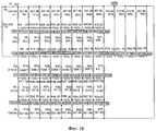
На фиг.1, 2 и 3 обозначено: 1 - первая прямоугольная диэлектрическая пластина; 2 - полосковый пленочный нагреватель, нанесенный на рабочую поверхность диэлектрической пластины 1; 3 - слой металла, нанесенный на тыльную поверхность диэлектрической пластины 1; 4 - датчик температуры, размещенный на рабочей поверхности диэлектрической пластины 1; 5 и 6 - элементы микросборок, размещенные на двух участках рабочей поверхности первой диэлектрической пластины 1 и залитые диэлектрическим компаундом; 7 и 8 - металлические брусочки прямоугольного сечения, механически соединенные с рабочей поверхностью диэлектрической пластины 1; 9 - вторая прямоугольная диэлектрическая пластина; 10 - слой металла, нанесенный на тыльную поверхность второй диэлектрической пластины 9; 11 и 12 - элементы микросборок, размещенные на двух участках рабочей поверхности второй диэлектрической пластины 9 и залитые диэлектрическим компаундом; 13 - блокировочный конденсатор; 14 - схема регулирования температуры; 15, 16, 17, 18, 19 и 20 - первая, вторая, третья, четвертая, пятая и шестая прямые линии, нанесенные на рабочую поверхность первой диэлектрической пластины 1 и визуально различимые от нее; 21 и 22 - седьмая и восьмая прямые линии, нанесенные на рабочую поверхность второй диэлектрической пластины 9 и визуально различимые от нее.In figure 1, 2 and 3 are indicated: 1 - the first rectangular dielectric plate; 2 - strip film heater deposited on the working surface of the
На фиг.4 и 5 обозначено: 23 - третья прямоугольная диэлектрическая пластина; 24 - слой металла, нанесенный на тыльную поверхность третьей диэлектрической пластины 23; 25 - элементы микросборок, размещенные на рабочей поверхности третьей диэлектрической пластины 23 и залитые диэлектрическим компаундом. Цифровые обозначения элементов второго варианта предлагаемого устройства с 1 по 22 совпадают с цифровыми обозначениями элементов первого варианта предлагаемого устройства (фиг.1, 2 и 3).In figures 4 and 5 are indicated: 23 - the third rectangular dielectric plate; 24 - a metal layer deposited on the back surface of the third
На фиг.6 приведена схема включения транзистора, при использовании его в качестве датчика температуры, а на фиг.7 - вольтамперные характеристики этого транзистора для двух значений ТОС.In Fig.6 shows a diagram of the inclusion of the transistor, when used as a temperature sensor, and Fig.7 is the current-voltage characteristics of this transistor for two values of TOC.
На фиг.8, а приведена схема распространения теплового потока от полоскового пленочного нагревателя в правой половине диэлектрической пластины устройства-прототипа [3] (на схеме тепловой поток направлен вдоль поперечной оси пластины Х к ее правому краю), а на фиг.8б показан характер убывания температуры в пластины при удалении от оси Y.On Fig, a shows the distribution of heat flux from the strip film heater in the right half of the dielectric plate of the prototype device [3] (in the diagram, the heat flux is directed along the transverse axis of the plate X to its right edge), and FIG. decrease in temperature in the plate with distance from the Y axis.
На фиг.9 приведены кривые зависимости температуры в различных точках прямоугольной пластины устройства-прототипа, выполненной из керамики ВК94, имеющей размеры 16, 12 и 1 мм, при разных значениях ТОС для случая, когда датчик температуры был расположен у края рабочей поверхности подложки на ее поперечной оси.Figure 9 shows the temperature curves at various points of the rectangular plate of the prototype device made of VK94 ceramics, having dimensions of 16, 12 and 1 mm, for different TOC values for the case when the temperature sensor was located at the edge of the working surface of the substrate on it transverse axis.
На фиг.10 приведена схема электрического моделирования зависимости температуры правой половины диэлектрической пластины, изображенной на фиг.8а, от координаты Х при Y=0 мм. Моделировалось распространение теплового потока по правой половине пластины, выполненной из керамики ВК94, имеющей коэффициент теплопроводности λ=13,2 Вт/(м·K). Полосковый пленочный нагреватель был расположен на оси Y по всей длине пластины (его ширина принималась пренебрежимо малой). Предполагалось, что внутри корпуса устройства для стабилизации температуры элементов микросборок тепловая конвекция отсутствовала. Приведенная степень черноты поверхности пластины ε принималась равной 0,8. Линейные размеры пластины составляли 16, 12 и 1 мм. Координата Z правого края пластины была равна +6 мм. Так как длина пластины была значительно больше половины ее ширины, то изменением температуры вдоль оси Y пренебрегали. Пунктирными линиями на фиг.10 показаны участки разбиения поверхности пластины на квадраты, при этом центры квадратов были расположены на оси X.Figure 10 shows a diagram of an electrical simulation of the temperature dependence of the right half of the dielectric plate shown in figa, from the coordinate X at Y = 0 mm The heat flux propagation along the right half of a plate made of VK94 ceramics with a thermal conductivity coefficient λ = 13.2 W / (m · K) was simulated. The strip film heater was located on the Y axis along the entire length of the plate (its width was assumed to be negligible). It was assumed that there was no thermal convection inside the body of the device to stabilize the temperature of the elements of microassemblies. The reduced degree of blackness of the surface of the plate ε was taken equal to 0.8. The linear dimensions of the plate were 16, 12, and 1 mm. The Z coordinate of the right edge of the plate was +6 mm. Since the length of the plate was much more than half its width, the temperature change along the Y axis was neglected. The dashed lines in Fig. 10 show the sections of dividing the plate surface into squares, with the centers of the squares being located on the X axis.
На фиг.11 приведены результаты моделирования зависимости температуры пластины от координаты Х при Y=0 мм, полученные в системе схемотехнического моделирования (ССМ) MicroCAP8, для схемы, изображенной на фиг.10, при разных значениях ТОС. На фиг.11а приведены результаты для значения ТОС 223 K, на фиг.11б - для значения ТОС 273 K и на фиг.11в - для значения ТОС 323 K.Figure 11 shows the results of modeling the dependence of the temperature of the plate on the X coordinate at Y = 0 mm, obtained in the MicroCAP8 circuit simulation system (CCM), for the circuit shown in figure 10, for different values of TOC. Fig. 11a shows the results for the TOC value of 223 K, Fig. 11b for the TOC value of 273 K and Fig. 11c for the TOC value of 323 K.
На фиг.12 приведены графики зависимостей температуры части пластины, изображенной на фиг.8а, от координаты Х при Y=0 мм. Графики построены для схемы, изображенной на фиг.10, по результатам моделирования, отображенным на фиг.11, для значений ТОС 223 K (кривая 1), 273 K (кривая 2) и 323 K (кривая 3).On Fig shows graphs of the temperature dependence of the part of the plate shown in figa, on the X coordinate at Y = 0 mm Graphs are plotted for the circuit depicted in FIG. 10, according to the simulation results shown in FIG. 11, for TOC values of 223 K (curve 1), 273 K (curve 2) and 323 K (curve 3).
На фиг.13 приведена схема электрического моделирования зависимостей температуры первой 1 и второй 9 прямоугольных диэлектрических пластин от координаты Х при Y=0 мм для первого варианта предлагаемого устройства для стабилизации температуры микросборок (фиг.1).In Fig.13 shows a diagram of an electrical simulation of the temperature dependences of the first 1 and second 9 rectangular dielectric plates on the X coordinate at Y = 0 mm for the first variant of the proposed device for stabilizing the temperature of microassemblies (Fig.1).
На фиг.14, 15 и 16 приведены результаты моделирования зависимости температуры первой 1 и второй 9 диэлектрических пластин (фиг.1) от координаты Х при Y=0 мм, полученные в ССМ MicroCAP8, для схемы, изображенной на фиг.13, при разных значениях ТОС. На фиг.14 приведены результаты моделирования для значения ТОС 223 K, на фиг.15 - для значения ТОС 273 K и на фиг.16 - для значения ТОС 323 K.Figures 14, 15 and 16 show the results of modeling the temperature dependence of the first 1 and second 9 dielectric plates (Fig. 1) on the X coordinate at Y = 0 mm, obtained in CCM MicroCAP8, for the circuit depicted in Fig. 13, for different TOC values. Fig. 14 shows the simulation results for the TOC value of 223 K, Fig. 15 - for the TOC value of 273 K and Fig. 16 - for the TOC value of 323 K.
На фиг.17 приведены кривые зависимости температуры первой 1 и второй 9 диэлектрических пластин (фиг.17а и 17б, соответственно) от координаты Х при Y=0 мм, построенные по результатам моделирования, отраженным на фиг.14, 15 и 16 для схемы, изображенной на фиг.13. Кривые 1 на этих фигурах отражают результаты моделирования для значения ТОС 223 K, кривые 2 - для значения ТОС 273 K и кривые 3 - для значения ТОС 323 K.In Fig.17 shows the curves of the temperature of the first 1 and second 9 dielectric plates (Figa and 17b, respectively) on the X coordinate at Y = 0 mm, constructed according to the simulation results reflected in Fig.14, 15 and 16 for the circuit, depicted in Fig.13.
На фиг.18 приведена схема электрического моделирования зависимости температуры первой 1, второй 9 и третьей 23 прямоугольных диэлектрических пластин от координаты Х при Y=0 мм для второго варианта предлагаемого устройства для стабилизации температуры микросборок (фиг.4).On Fig is a diagram of the electrical simulation of the temperature dependence of the first 1, second 9 and third 23 rectangular dielectric plates on the X coordinate at Y = 0 mm for the second variant of the proposed device for stabilizing the temperature of microassemblies (figure 4).
На фиг.19, 20 и 21 приведены результаты моделирования зависимости температуры первой 1, второй 9 и третьей 23 прямоугольных диэлектрических пластин от координаты Х при Y=0 мм для второго варианта предлагаемого устройства для стабилизации температуры микросборок (фиг.4) при разных значениях ТОС. На фиг.19 приведены результаты моделирования для значения ТОС 223 K, на фиг.20 - для значения ТОС 273 K и на фиг.21 - для значения ТОС 323 K.On Fig, 20 and 21 shows the simulation results of the temperature dependence of the first 1, second 9 and third 23 rectangular dielectric plates on the X coordinate at Y = 0 mm for the second variant of the proposed device for stabilizing the temperature of microassemblies (figure 4) at different values of TOC . In Fig.19 shows the simulation results for the TOC value of 223 K, Fig.20 for the TOC value of 273 K and Fig.21 for the TOC value of 323 K.
На фиг.22 изображены кривые зависимости температуры первой 1, второй 9 и третьей 23 прямоугольных диэлектрических пластин (фиг.22а, фиг.22б и фиг.22в соответственно) от координаты Х при Y=0 мм для второго варианта предлагаемого устройства для стабилизации температуры микросборок (фиг.4). Кривые построены по результатам моделирования, отраженным на фиг.19, 20 и 21. Кривые 1 на этих фигурах соответствуют результатам моделирования для значения ТОС 223 K, кривые 2 - для значения ТОС 273 K и кривые 3 - для значения ТОС 323 K.On Fig shows the temperature dependence of the first 1, second 9 and third 23 rectangular dielectric plates (figa, figb and figv respectively) from the X coordinate at Y = 0 mm for the second variant of the proposed device for stabilizing the temperature of microassemblies (figure 4). The curves are plotted according to the simulation results shown in Figs. 19, 20 and 21.
Оба варианта устройства для стабилизации температуры микросборок (фиг.1 и 4) работают следующим образом. Температура термостатирования выбирается больше ТОС. Поэтому при подключении устройства к источнику питания температура первой прямоугольной диэлектрической пластины 1 и температура транзистора VT, примененного в качестве датчика температуры 4 (фиг.6), оказываются ниже температуры термостатирования. При этой температуре ток коллектора транзистора IK0 мал, а напряжение на коллекторе UK велико. Увеличение напряжения UK, приложенного к входу дифференциального усилителя, входящего в схему регулирования температуры 14, приводит к увеличению тока через полосковый пленочный нагреватель 2, подключенный к выходу дифференциального усилителя. Мощность, выделяемая полосковым пленочным нагревателем, вызывает перегрев первой прямоугольной диэлектрической пластины 1 ΔТП, равный разности между температурой этой пластины ТП и ТОС-TOC. В этом случае ΔТП=ТП-ТОС. При этом нагрев первой пластины 7 и датчика температуры 4, расположенного на рабочей поверхности пластины, постепенно увеличивается до температуры термостатирования. Увеличение температуры пластины 1 выше температуры термостатирования приводит к увеличению значения тока коллектора транзистора IK0, к уменьшению значений напряжения коллектора UK и тока через полосковый пленочный нагреватель 2. При этом температура первой пластины 7 уменьшается до температуры термостатирования. В дальнейшем процесс повторяется. Заданный диапазон изменения температуры термостатирования ΔTCT.З определяет точность регулирования температуры пластины в районе размещения датчика температуры 4.Both versions of the device for stabilizing the temperature of microassemblies (figures 1 and 4) work as follows. Thermostat temperature is selected more than CBT. Therefore, when connecting the device to the power source, the temperature of the first rectangular
В качестве датчика температуры 4 был применен бескорпусной биполярный транзистор малых размеров, что уменьшило тепловую инерционность датчика и увеличило динамическую точность регулирования температуры. Коллектор транзистора, электрически соединенный с входом дифференциального усилителя, входящего в схему регулирования температуры, был включен по схеме с общим эмиттером (фиг.6). Из вольтамперных характеристик транзистора (фиг.7) видно, что при постоянном задающем напряжении UЭБ0, поступающем на базу транзистора VT с резистора R2, увеличение ТОС от значения T1 до значения T2 приводит к увеличению тока коллектора IК0, что, в свою очередь, вызывает уменьшение напряжения на коллекторе UК. Напряжение с коллектора UК поступает на один из входов дифференциального усилителя схемы регулирования температуры, с выходом которого соединен полосковый пленочный нагреватель 2, расположенный на рабочей поверхности пластины 7. Уменьшение напряжения на коллекторе UК вызывает уменьшение тока через полосковый пленочный нагреватель 2 и уменьшение температуры пластины 1. При уменьшении TOC и температуры ТП пластины 1 напряжение на коллекторе UК транзистора увеличивается, что приводит к увеличению тока через полосковый пленочный нагреватель 2 и к увеличению температуры ТП пластины 1. Величину температуры термостатирования TCT пластины 1 можно изменять, меняя опорное напряжение на другом входе дифференциального усилителя схемы регулирования температуры.As a
В предлагаемых вариантах устройств (фиг.1 и 4), точность термостатирования элементов, расположенных в ограниченных областях рабочей поверхности прямоугольной диэлектрической пластины 1, оказывается выше точности термостатирования пластины в районе размещения датчика температуры 4. Это подтверждается расчетом температурного поля этой пластины.In the proposed device variants (Figs. 1 and 4), the accuracy of temperature control of elements located in limited areas of the working surface of a
Вначале рассмотрим расчет температурного поля диэлектрической пластины при отсутствии металлического слоя 3 (металлический слой отсутствует в устройстве-прототипе). Если пренебречь изменением температуры вдоль продольной оси пластины Y, то расчет температурного поля пластины сводится к решению одномерной задачи распространения теплового потока вдоль пластины (фиг.8, а и б), приведенному в [4]. Формула для расчета температурного поля пластины при пренебрежении шириной нагревателя имеет вид:First, we consider the calculation of the temperature field of the dielectric plate in the absence of a metal layer 3 (the metal layer is absent in the prototype device). If we neglect the temperature change along the longitudinal axis of the plate Y, then the calculation of the temperature field of the plate reduces to solving the one-dimensional problem of heat flux propagation along the plate (Fig. 8, a and b), given in [4]. The formula for calculating the temperature field of the plate when neglecting the width of the heater is:
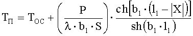
где ТП - температура пластины; TOC - температура окружающей среды; λ - коэффициент теплопроводности материала пластины; l - половина ширины пластины; Р - тепловой поток, равный по величине половине тепловой мощности нагревателя;where T P - plate temperature; T OC is the ambient temperature; λ is the coefficient of thermal conductivity of the plate material; l is half the width of the plate; P is the heat flux equal to half the heat output of the heater;
S=а·δ - площадь поперечного сечения пластины; а - длина пластины; U=1(а+δ) - периметр поперечного сечения пластины; l1=l+S/U - эффективная длина, численное значение которой используется в расчете температурного поля пластины; (b1)2=α·U/(λ·S) - коэффициент, определяющий скорость убывания температуры при удалении от нагревателя (при возрастании координаты X); α=αк+αл - коэффициент теплоотдачи; αк - конвективно-кондуктивный коэффициент теплоотдачи; αл - коэффициент теплоотдачи излучением.S = a · δ is the cross-sectional area of the plate; a is the length of the plate; U = 1 ( a + δ) is the perimeter of the cross section of the plate; l 1 = l + S / U is the effective length, the numerical value of which is used in the calculation of the temperature field of the plate; (b 1 ) 2 = α · U / (λ · S) - coefficient that determines the rate of decrease of temperature with distance from the heater (with increasing coordinate X); α = α to + α l - heat transfer coefficient; α to - convective-conductive heat transfer coefficient; α l - heat transfer coefficient by radiation.
Проведенный более точный расчет температурного поля пластины, используемой в [3], сводится к решению двумерной задачи распространения теплового потока от пленочного нагревателя путем математического моделирования с учетом регулирования температуры. Результаты такого расчета приведены на фиг.9. Заданный диапазон изменения температуры термостатирования в районе размещения датчика температуры составлял ΔTCT.З≤5 K. Максимальная тепловая мощность нагревателя PMAX составляла 2,2 Вт. Диапазон изменения температуры внешней среды ΔTOC=100 K находился в пределах 223…323 K. Температура термостатирования ТСТ составляла 334 K. Точность термостатирования в различных точках поверхности пластины в широком диапазоне изменения ТОС неодинакова. Из графиков изменения температуры вдоль оси Х при фиксированном значении координаты Y (фиг.9) видно, что точность термостатирования элементов, расположенных в ограниченных областях поверхности пластины вблизи координат Х=+4 мм и Х=-4 мм, оказывается выше точности термостатирования пластины в районе размещения датчика температуры Х=+6 мм. Для различных значений координаты Y, графики изменения температуры вдоль оси Х почти не отличаются друг от друга, когда длина пластины значительно превышает половину ее ширины [3]. Это означает, что с высокой точностью можно моделировать изменение температуры вдоль оси X, решая одномерную задачу, не учитывая изменение температуры вдоль оси Y.A more accurate calculation of the temperature field of the plate used in [3] is reduced to solving the two-dimensional problem of the propagation of heat flux from a film heater by mathematical modeling taking into account temperature control. The results of this calculation are shown in Fig.9. The predetermined range of temperature control in the temperature sensor location was ΔT CT.З ≤5 K. The maximum thermal power of the heater P MAX was 2.2 W. The range of changes in ambient temperature ΔT OC = 100 K was in the
С помощью моделирования докажем эффективность применения заявляемых вариантов устройства для стабилизации температуры микросборок (фиг.1 и 4) по сравнению с устройством-прототипом.Using modeling, we prove the effectiveness of the application of the claimed variants of the device for stabilizing the temperature of microassemblies (Figs. 1 and 4) in comparison with the prototype device.
При электрическом моделировании зависимости температуры пластины ТП от координаты Х при Y=0 мм (фиг.10) величина напряжения VH в В численно принималась равной величине температуры нагревателя (TH) в Кельвинах (K), а величина напряжения VC в В - величине ТОС в K. Электрическое сопротивление Rλ в Ом принималось численно равным тепловому сопротивлению квадрата пластины (пластина разбивалась на отдельные квадраты) RλT=1/(λ·δ)=1/(13,2·1·10-3)≈76 K/Вт [5]. Электрическое сопротивление Ri в Ом выбиралось численно равным тепловому сопротивлению RiT между площадью квадрата разбиения пластины, участвующей в лучистом теплообмене, и окружающей средой, в K/Вт. Величину RiT определяли с помощью выражения [4]In the electrical simulation of the dependence of the temperature of the plate T P on the X coordinate at Y = 0 mm (Fig. 10), the voltage value V H in V was numerically taken equal to the value of the heater temperature (T H ) in Kelvins (K), and the voltage value V C in V - the value of T OS in K. The electrical resistance R λ in Ohms was taken numerically equal to the thermal resistance of the square of the plate (the plate was divided into separate squares) R λT = 1 / (λ · δ) = 1 / (13.2 · 1 · 10 -3 ) ≈76 K / W [5]. The electrical resistance R i in Ohms was chosen numerically equal to the thermal resistance R iT between the square of the partition of the plate involved in the radiant heat transfer and the environment, in K / W. The value of R iT was determined using the expression [4]
RiT=(αл·Si)-1,R iT = (α l · S i ) -1 ,
где Si=(2·0,5·10-3)2 м2=0,5·10-6 м2 - площадь квадрата, участвующая в лучистом теплообмене, при разбиении поверхности пластины на квадраты; αл=ε·f(ТП, TOC) - коэффициент теплообмена излучением; ![]()
![]()
Температура ТП при вычислении αл выбрана равной ТСТ для всех квадратов, так как ТП-TCT<<ТП (по этой же причине сопротивления Ri соединены с центрами квадратов площадей рабочей поверхности пластины, хотя учитывают теплообмен с рабочей и с тыльной стороны поверхностей пластины).The temperature T P in the calculation of α l was chosen equal to T CT for all squares, since T P -T CT << T P (for the same reason, the resistances R i are connected to the centers of squares of the areas of the working surface of the plate, although heat exchange with the working and back of plate surfaces).
Из расчетов следует: Ri=490,8 кОм для TOC=223 K, Ri=390,4 кОм для TOC=273 K и Ri=310,9 кОм для TOC=323 K. Мощностью, отводимой с небольших (относительно общей площади теплообмена) торцевых поверхностей пластины, пренебрегли [4].It follows from the calculations: R i = 490.8 kΩ for T OC = 223 K, R i = 390.4 kΩ for T OC = 273 K and R i = 310.9 kΩ for T OC = 323 K. small (relative to the total heat transfer area) end surfaces of the plate were neglected [4].
При моделировании в ССМ MicroCAP [6] зависимости температуры пластины ТП от координаты Х при Y=0 мм (фиг.11), температура термо-статирования была выбрана TCT=334 K. Диапазон ее изменения в районе размещения датчика температуры составил ΔTCT=333,907-333,783=0,124 K. Температура правого края пластины оказалась равной 333,783 K для TOC=223 K; 333,835 K для TOC=273 K и 333,907 K для TOC=323 K.When simulating in the MicroCAP CCM [6] the dependence of the temperature of the plate T P on the X coordinate at Y = 0 mm (Fig. 11), the temperature of thermo-stating was chosen T CT = 334 K. The range of its change in the region of the temperature sensor was ΔT CT = 333.907-333.783 = 0.124 K. The temperature of the right edge of the plate turned out to be 333.783 K for T OC = 223 K; 333.835 K for T OC = 273 K and 333.907 K for T OC = 323 K.
В схеме электрического моделирования зависимостей температуры первой 1 и второй 9 прямоугольных диэлектрических пластин от координаты Х при Y=0 мм для первого варианта предлагаемого устройства, приведенной на фиг.13, моделировалось распространение теплового потока по правым половинам обеих пластин. Размеры и теплофизические характеристики первой диэлектрической пластины 1 в этой конструкции устройства были такие же, как и у пластины, для которой составлена схема электрического моделирования зависимости температуры подложки ТП от координаты Х (при Y=0 мм), приведенная на фиг.10. Электрическое сопротивление Rλ в Ом принималось численно равным тепловому сопротивлению квадрата подложки Rλ1T=1/(λ·δ1)=1/(13,2·1·10-3) K/Вт ≈ 76 K/Вт и Rλ1=76 Ом.In the circuit of electrical modeling of the temperature dependences of the first 1 and second 9 rectangular dielectric plates on the X coordinate at Y = 0 mm for the first variant of the proposed device, shown in Fig. 13, the heat flux propagation along the right halves of both plates was simulated. The dimensions and thermophysical characteristics of the first
В первый вариант предлагаемого устройства (фиг.1), в отличие от устройства-прототипа, дополнительно введен размещенный на тыльной стороне поверхности диэлектрической пластины 1 слой металла 3, обладающий высокой теплопроводностью. Длина слоя равна длине диэлектрической пластины, а ширина - расстоянию между пятой 19 и шестой 20 прямыми линиями, нанесенными на рабочую поверхность пластины. Координаты Х этих линий выбирают в области, где погрешность термостатирования имеет наименьшее значение. В нашем случае ширина металлического слоя 3 равна 8 мм (ограничена прямыми с координатами Х=±4 мм). Слой металла был изготовлен из меди, имеющей коэффициент теплопроводности λM=390 Вт/(м·K). Толщина этого слоя составляла δM=128,2 мкм, что соответствует тепловому сопротивлению квадрата металлического слоя RПЛТ=1/(λМ·δМ)=1/(390·128,2·10-6) K/Вт ≈ 20 K/Вт и RПЛ=20 Ом. Возможно изготовление слоя 3 и из других металлов, обладающих высокими значениями коэффициентов теплопроводности (из серебра - λМ=410 Вт/(м·K), из золота - λМ=300 Вт/(м·K), из алюминия - λМ=210 Вт/(м·K)). Слои 5 и 6, содержащие элементы микросборок, размещенные на двух участках диэлектрической пластины 7, залиты диэлектрическим компаундом холодного отверждения, обладающим высоким коэффициентом теплопроводности, и служат для электрической изоляции элементов. Слои 11 и 12, размещенные на рабочей поверхности второй диэлектрической пластины 9, залиты таким же компаундом. Слои 5 и 11 и слои 6 и 12 соприкасаются между собой. Для упрощения схемы электрического моделирования эти слои представлены на схеме электрического моделирования (фиг.13) как один слой. Его ширина равна 7 мм и ограничена прямыми с координатами Х=±3,5 мм. Суммарная толщина этих слоев δС=0,4·10-3 м. Для герметизации элементов микросборок используют диэлектрические компаунды холодного отверждения, клеи и стекла [7]. Коэффициент теплопроводности у стекла С48-3 равен 1,5 Вт/(м·K), у компаунда ЭК16А - 0,35 Вт/(м·K), у теплопроводящих клеев - до 0,8 Вт/(м·K). Элементы микросборок, имеющие коэффициент теплопроводности порядка 20 Вт/(м·K), повышают эквивалентный коэффициент теплопроводности λЭ слоев 5, 6, 11 и 12. Примем эквивалентный коэффициент теплопроводности этих слоев λЭ=1,5 Вт/(м·K). Тепловое сопротивление квадрата слоев RλCT=1/(λЭ·δC)=1/(1,5·0,4·10-3) K/Вт ≈ 1666,6 K/Вт. Сопротивление RλC=1666,6 Ом в модели не учитываем, так как оно намного больше Rλ1=76 Ом, и его шунтирующее действие пренебрежимо мало. Вторая прямоугольная диэлектрическая пластина 9 (фиг.1 и 3) изготовлена из керамики ВК94. Ее ширина равна 7 мм и ограничена прямыми с координатами Х=±3,5 мм. Толщина этой пластины δ2=0,6 мм. Тепловое сопротивление квадрата RλT2=1/(λ·δ2)=1/(13,2·0,6·10-3) K/Вт ≈ 126,26 K/Вт, Rλ2=126 Ом. Слой металла 10, нанесенный на тыльную поверхность второй диэлектрической пластины 9, обладает высоким коэффициентом теплопроводности. Авторами для изготовления слоя металла 10 была выбрана медь. Ширина слоя металла была равна 7 мм (она была ограничена прямыми с координатами Х=±3,5 мм). Толщина этого слоя была равна 128,2 мкм, а RПЛ=20 Ом. Для изготовления брусочков 7 и 8 (фиг.1 и 4) также была выбрана медь. Размер брусочков вдоль оси координат Х равен 0,5 мм, а вдоль оси Y 1,13 мм. Расстояние между внешними гранями брусочков выбрано равным ширине металлического слоя 3, размещенного на тыльной стороне диэлектрической пластины 1.In the first embodiment of the proposed device (Fig. 1), in contrast to the prototype device, a
Для схемы электрического моделирования, приведенной на фиг.13, были получены расчетные значения Ri такие же, как для схемы, изображенной на фиг.10, а именно: Ri=490,8 кОм для TOC=223 K, Ri=390,4 кОм для TOC=273 K и Ri=310,9 кОм для TOC=323 K. Тепловое сопротивление RZT в K/Вт между площадью квадрата разбиения For the electrical simulation circuit shown in Fig. 13, the calculated values of R i were obtained as for the circuit shown in Fig. 10, namely: R i = 490.8 kOhm for T OC = 223 K, R i = 390.4 kΩ for T OC = 273 K and R i = 310.9 kΩ for T OC = 323 K. Thermal resistance R ZT in K / W between the square of the split
Si=(0,5·10-3)2 м2=0,25·10-6 м2 рабочей поверхности диэлектрической пластины 7 и площадью квадрата разбиения слоя металла 3, нанесенного на тыльной поверхности этой пластины, равно RZT=δ1/(λ·Si)=10-3/(13,2·0,52·10-6) K/Вт ≈ 303 K/Вт, что соответствует электрическому сопротивлению на модели RZ=303 Ом. Тепловое сопротивление RZ1T в K/Вт между площадью квадрата разбиения Si рабочей поверхности диэлектрической пластины 1 и площадью квадрата разбиения рабочей стороны второй диэлектрической пластины 9 равноS i = (0.5 · 10 -3 ) 2 m 2 = 0.25 · 10 -6 m 2 of the working surface of the dielectric plate 7 and the square area of the partition of the
RZ1T=δC/(λC·Si)=0,4·10-3/(1,5·0,52·10-6) K/Вт ≈ 1066,7 K/Вт,R Z1T = δ C / (λ C · S i ) = 0.4 · 10 -3 / (1.5 · 0.5 2 · 10 -6 ) K / W ≈ 1066.7 K / W,
что соответствует электрическому сопротивлению на схеме электрического моделирования (фиг.13) RZ1=1066,7 Ом. Тепловое сопротивление RZ2T в K/Вт между площадью квадрата разбиения Si тыльной стороны второй диэлектрической пластины 9 и площадью квадрата разбиения слоя металла 10 было равно RZ2T=δ2/(λ·Si)=0,6·10-3/(13,2·0,52·10-6) K/Вт ≈ 181,8 K/Вт, что соответствует сопротивлению на схеме электрического моделирования RZ2=181,8 Ом. Тепловое сопротивление RШ1Т вдоль оси Z части брусочка 8, шунтирующей тепловое сопротивление модели RZ1T находим по формуле: RШ1Т=2·δШ1/(λШ·Si)=2·0,4·10-3/(390·0,52·10-6) K/Вт ≈ 8,2 K/Вт, где λШ=390 Вт/(м·К), а δШ1=0,4·10-3 м. На электрической модели RШ1=8,2 Ом. Тепловое сопротивление RШ2Т вдоль оси Z части брусочка 8, шунтирующей тепловое сопротивление модели RZ2T находим по формуле RШ2Т=2·δШ2/(λШ·Si)=2·0,7·10-3/(390·0,52·10-6) K/Вт ≈ 14,36 K/Вт, где δШ2=0,7·10-3 м. На электрической модели RШ2=14,36 Ом.which corresponds to the electrical resistance in the circuit of electrical modeling (Fig) R Z1 = 1066.7 Ohms. The thermal resistance R Z2T in K / W between the square of the partition S i of the back of the second dielectric plate 9 and the square of the partition of the
Проведем сравнительный анализ результатов моделирования зависимости температуры диэлектрических пластин 1 и 9 (фиг.1) от координаты Х при Y=0 мм для первого варианта предлагаемого устройства (фиг.14, 15, 16, 17а и 17б) и результатов моделирования зависимости температуры диэлектрической пластины от координаты Х при Y=0 мм для устройства-прототипа (фиг.12). Для этого сравним площади зон с малой погрешностью термостатирования, найденные по графикам, изображенным на фиг.12, с площадями зон, найденными по графикам зависимостей температуры диэлектрических пластин 7 и 9 от координаты Х при Y=0 мм (фиг.17а и б). Из анализа графиков зависимостей, представленных на фиг.12, следует, что температура подложки меняется на 0,1 K от 334 K до 334,1 K в диапазоне ТОС от 223 K до 323 K при изменении координаты Х от Х1=+3,5 мм до X2=+4 мм. Такое изменение происходит на площади подложки, занятой элементами, S1=2·(Х2-X1)·L, где L - длина подложки в мм. В этом случае S1=1·L мм2. Из анализа зависимостей, представленных на фиг.17а, следует, что температура диэлектрической пластины 1 меняется на 0,1 K от 333,93 K до 334,03 K в диапазоне ТОС от 223 K до 323 K при изменении координаты Х от Х1=+2,75 мм до Х2=+4 мм. Такое изменение происходит на площади диэлектрической пластины 1, занятой элементами, S01=2·(X2-X1)·L=2,5·L мм2. Из анализа графика зависимостей, представленных на фиг.17б, следует, что температура второй диэлектрической пластины Р меняется на 0,081 K от 333,93 K до 334,011 K в диапазоне ТОС от 223 K до 323 K при изменении координаты Х от Х1=+0 мм до Х2=+4 мм. Такое изменение происходит на площади второй диэлектрической пластины 9, занятой элементами, S02=2·(Х2-X1)·L=8·L мм2. Суммарная площадь SC1, занятая элементами, на которой температура диэлектрической пластины 1 и второй диэлектрической пластины 9 меняется на величину ≤0,1 K в диапазоне ТОС от 223 K до 323 K равна SC1=S01+S02=10,5·L мм2. Площадь, занятая элементами микросборок, на которой температура пластин меняется на величину ≤0,1 K, в первом варианте предлагаемого устройства по сравнению с устройством-прототипом увеличивается в число, вычисляемое из отношения SC1 к S1, то есть для рассмотренных устройств в 10,5 раз.A comparative analysis of the simulation results of the temperature dependence of the
Во второй вариант предлагаемого устройства для стабилизации температуры микросборок (фиг.4), в отличие от первого варианта (фиг.1), дополнительно введены: третья диэлектрическая пластина 23 (фиг.4), на тыльной поверхности которой расположен слой металла 24, и элементы микросборок 25 размещены на всей рабочей поверхности диэлектрической пластины 23 и залиты диэлектрическим компаундом холодного отверждения. В схеме электрического моделирования зависимостей температуры первой прямоугольной диэлектрической пластины 1, второй диэлектрической пластины 9 и третьей диэлектрической пластины 23 от координаты Х при Y=0 мм для второго варианта предлагаемого устройства, приведенной на фиг.18, моделировалось распространение теплового потока по правым половинам этих пластин. Величины номинальных значений новых (по сравнению со схемой на фиг.13) видов сопротивлений в схеме, представленной на фиг.18, равны Rλ3=Rλ2=126 Ом; RZ3=RZ1=1066,7 Ом; RZ4=RZ2=181,8 Ом; RШ3=RШ1=8,20 м; RШ4=RШ2=14,36 Ом.In the second variant of the proposed device for stabilizing the temperature of the microassemblies (Fig. 4), in contrast to the first variant (Fig. 1), the following are additionally introduced: a third dielectric plate 23 (Fig. 4), on the back surface of which there is a
Проведем сравнительный анализ результатов моделирования зависимости температуры первой 1, второй 9 и третьей 23 прямоугольных диэлектрических пластин от координаты Х при Y=0 мм для второго варианта предлагаемого устройства (фиг.19, 20, 21, 22 а, б и в) и результатов моделирования зависимости температуры подложки от координаты X при Y=0 мм для устройства-прототипа (фиг.12). Для этого сравним площади зон с малой погрешностью термостатирования, найденные из зависимостей температуры подложки от координаты Х при Y=0 мм, изображенных на фиг.12, с найденными зависимостями температуры от координаты Х при Y=0 мм для первой 1, второй 9 и третьей 23 прямоугольных диэлектрических пластин (фиг.22 а, б и в). Из анализа графика зависимостей, представленных на фиг.12, следует, что температура подложки меняется на 0,1 K от 334 K до 334,1 K на площади подложки, занятой элементами, S1=1·L мм2, где L - длина подложки в мм. Из анализа графика зависимостей, приведенных на фиг.22а, следует, что температура диэлектрической пластины 1 меняется на 0,1 K от 333,93 K до 334,03 K в диапазоне ТОС от 223 K до 323 K при изменении координаты Х от Х1=+2,75 мм до Х2=+4 мм. Такое изменение происходит на площади диэлектрической пластины 1, занятой элементами, S01=2·(Х2-X1)·L=2.5·L мм2. Из анализа графика зависимостей, приведенных на фиг.22б следует, что температура второй диэлектрической пластины 9 меняется на 0,081 K от 333,93 K до 334,011 K в диапазоне ТОС от 223 K до 323 K при изменении координаты Х от Х1=+0 мм до Х2=+4 мм. Такое изменение происходит на площади диэлектрической пластины 9, занятой элементами, SД1=2·(Х2-X1)·L=8·L мм2. Из этого следует, что для рассматриваемого примера элементы микросборок могут быть размещены по всей рабочей поверхности диэлектрической пластины 9. Из анализа зависимостей, приведенных на фиг.22в, следует, что температура третьей диэлектрической пластины 23 меняется на 0,026 K от 333,929 K до 333,903 K в диапазоне ТОС от 223 K до 323 K при изменении координаты Х от Х1=+4 мм до Х2=+0 мм. Такое изменение происходит на площади третьей диэлектрической пластины 23, занятой элементами микросборок, SД2=2·|(X2-X1)|·L=8·L, мм2. Суммарная площадь SC2, занятая элементами микросборок, на которой температура первой 1, второй 9 и третьей 23 диэлектрических пластин меняется на величину ≤0,1 K в диапазоне ТОС от 223 K до 323 K, равна SC2=S01+SД1+SД2=18,5·L.A comparative analysis of the simulation results of the temperature dependence of the first 1, second 9 and third 23 rectangular dielectric plates on the X coordinate at Y = 0 mm for the second variant of the proposed device (Fig. 19, 20, 21, 22 a, b and c) and simulation results the dependence of the substrate temperature on the X coordinate at Y = 0 mm for the prototype device (Fig. 12). To do this, we compare the area of the zones with a small thermostating error found from the dependences of the substrate temperature on the X coordinate at Y = 0 mm shown in Fig. 12 with the found temperature dependences on the X coordinate at Y = 0 mm for the first 1, second 9, and third 23 rectangular dielectric plates (Fig. 22 a, b and c). From the analysis of the dependency graph shown in Fig. 12, it follows that the temperature of the substrate varies by 0.1 K from 334 K to 334.1 K in the area of the substrate occupied by the elements, S 1 = 1 · L mm 2 , where L is the length substrate in mm. From the analysis of the dependency graph shown in figa, it follows that the temperature of the
Площадь, занятая элементами микросборок, на которой температура пластин меняется на величину ≤0,1 K, во втором варианте предлагаемого устройства по сравнению с устройством-прототипом увеличивается в число, вычисляемое из отношения SC2 к S1, то есть для сравниваемых устройств эта площадь увеличивается в 18,5 раз.The area occupied by the elements of microassemblies, on which the temperature of the plates varies by ≤0.1 K, in the second embodiment of the proposed device, compared with the prototype device, increases in the number calculated from the ratio S C2 to S 1 , that is, for the compared devices this area increases by 18.5 times.
Таким образом, первый и второй варианты предлагаемых устройств для стабилизации температуры микросборок имеют существенно большую площадь с малой погрешностью термостатирования по сравнению с устройством-прототипом (в наших примерах больше соответственно в 10,5 и в 18,5 раз). Длина и ширина сравниваемых устройств была одинакова, высота возросла не более чем в четыре раза. Габаритные размеры предлагаемых устройств в корпусах и габаритные размеры устройства-прототипа в корпусе почти не отличаются.Thus, the first and second variants of the proposed devices for stabilizing the temperature of microassemblies have a significantly larger area with a small thermostating error compared to the prototype device (in our examples, 10.5 and 18.5 times more, respectively). The length and width of the compared devices was the same, the height increased by no more than four times. The overall dimensions of the proposed devices in the cases and the overall dimensions of the prototype device in the case are almost the same.
Источники информацииInformation sources
1. Авт.свид. СССР №1672421, кл. G05D 23/19. Бабаян P.P., Окропидзе Д.П., Ованесян О.Г. Устройство для термостатирования полупроводниковых пластин интегральных микросхем. Опубл. 23.08.91. Бюл. №31.1. Autosvid. USSR No. 1672421, cl.
2. Пат. РФ №2355016, кл. G05D 23/19. Козлов В.Г., Алексеев В.П., Карабан В.М. Устройство стабилизации температуры электрорадиоэлементов. Опубл. 10.05.2009. Бюл. №13.2. Pat. RF №2355016,
3. Пат. РФ №2348962, кл. G05D 23/19. Козлов В.Г., Алексеев В.П., Карабан В.М. Устройство для стабилизации температуры элементов микросхем и микросборок. Опубл. 10.03.2009. Бюл. №7 - прототип.3. Pat. RF №2348962,
4. Дульнев Г.Н. Тепломассообмен в радиоэлектронной аппаратуре. - М.: Высш. шк., 1984. - 247 с. (с.41-46 и с.95).4. Dulnev G.N. Heat and mass transfer in electronic equipment. - M .: Higher. school., 1984. - 247 p. (p. 41-46 and p. 95).
5. Козлов В.Г. Практикум по тепломассообмену. Томск: Изд-во Томск. ун-та, 1980. - 75 с. (с.46-57).5. Kozlov V.G. Workshop on heat and mass transfer. Tomsk: Tomsk Publishing House. University, 1980 .-- 75 p. (p. 46-57).
6. Разевиг В.Д. Схемотехническое моделирование с помощью Micro-Cap 7. - М.: Горячая линия - Телеком, 2003.6. Razevig V.D. Circuit modeling using Micro-Cap 7. - M .: Hot line - Telecom, 2003.
7. Конструирование и технология микросхем. Под ред. Л.А.Коледова. - М.: Высш. шк., 1984. - 231 с. (с.96 и с.171).7. Design and technology of microcircuits. Ed. L.A. Koledova. - M .: Higher. school., 1984. - 231 p. (p. 96 and p. 171).
Claims (2)
Priority Applications (1)
| Application Number | Priority Date | Filing Date | Title |
|---|---|---|---|
| RU2010140166/08A RU2459231C2 (en) | 2010-09-30 | 2010-09-30 | Device to stabilise temperature of microassemblies |
Applications Claiming Priority (1)
| Application Number | Priority Date | Filing Date | Title |
|---|---|---|---|
| RU2010140166/08A RU2459231C2 (en) | 2010-09-30 | 2010-09-30 | Device to stabilise temperature of microassemblies |
Publications (2)
| Publication Number | Publication Date |
|---|---|
| RU2010140166A RU2010140166A (en) | 2012-04-10 |
| RU2459231C2 true RU2459231C2 (en) | 2012-08-20 |
Family
ID=46031349
Family Applications (1)
| Application Number | Title | Priority Date | Filing Date |
|---|---|---|---|
| RU2010140166/08A RU2459231C2 (en) | 2010-09-30 | 2010-09-30 | Device to stabilise temperature of microassemblies |
Country Status (1)
| Country | Link |
|---|---|
| RU (1) | RU2459231C2 (en) |
Citations (6)
| Publication number | Priority date | Publication date | Assignee | Title |
|---|---|---|---|---|
| SU1672421A1 (en) * | 1989-09-05 | 1991-08-23 | Институт проблем управления | Wafers thermostating unit |
| EP0456398A2 (en) * | 1990-05-04 | 1991-11-13 | AT&T Corp. | Cooling of electronic equipment cabinets |
| US5067040A (en) * | 1990-09-24 | 1991-11-19 | Joel Fallik | Expandable refrigerated enclosure for computer boards |
| EP0878990A1 (en) * | 1997-05-17 | 1998-11-18 | BODENSEEWERK GERÄTETECHNIK GmbH | Heat protective jacket for an electronic device |
| RU2348962C1 (en) * | 2007-05-22 | 2009-03-10 | ГОУ ВПО "Томский государственный университет систем управления и радиоэлектроники" | Device for stabilisation of temperature of devices of microcircuits and microassemblies |
| RU2355016C2 (en) * | 2007-03-15 | 2009-05-10 | ГОУ ВПО "Томский государственный университет систем управления и радиоэлектроники" | Device for stabilising temperature of radio components |
-
2010
- 2010-09-30 RU RU2010140166/08A patent/RU2459231C2/en not_active IP Right Cessation
Patent Citations (6)
| Publication number | Priority date | Publication date | Assignee | Title |
|---|---|---|---|---|
| SU1672421A1 (en) * | 1989-09-05 | 1991-08-23 | Институт проблем управления | Wafers thermostating unit |
| EP0456398A2 (en) * | 1990-05-04 | 1991-11-13 | AT&T Corp. | Cooling of electronic equipment cabinets |
| US5067040A (en) * | 1990-09-24 | 1991-11-19 | Joel Fallik | Expandable refrigerated enclosure for computer boards |
| EP0878990A1 (en) * | 1997-05-17 | 1998-11-18 | BODENSEEWERK GERÄTETECHNIK GmbH | Heat protective jacket for an electronic device |
| RU2355016C2 (en) * | 2007-03-15 | 2009-05-10 | ГОУ ВПО "Томский государственный университет систем управления и радиоэлектроники" | Device for stabilising temperature of radio components |
| RU2348962C1 (en) * | 2007-05-22 | 2009-03-10 | ГОУ ВПО "Томский государственный университет систем управления и радиоэлектроники" | Device for stabilisation of temperature of devices of microcircuits and microassemblies |
Also Published As
| Publication number | Publication date |
|---|---|
| RU2010140166A (en) | 2012-04-10 |
Similar Documents
| Publication | Publication Date | Title |
|---|---|---|
| CN111132391B (en) | Integrated heater and sensor system | |
| US7714694B2 (en) | Compensating for linear and non-linear trimming-induced shift of temperature coefficient of resistance | |
| CN107389206A (en) | A kind of thermopile sensor and its control method | |
| KR102303306B1 (en) | holding device | |
| CN110873730B (en) | Measuring device for determining the thermal conductivity of a fluid | |
| KR20050026904A (en) | Method for trimming resistors | |
| CN110022981A (en) | Temperature-controlled appliance | |
| KR101489900B1 (en) | Liquid metal circuit device and control method liquid metal circuit device | |
| RU2355016C2 (en) | Device for stabilising temperature of radio components | |
| RU2459231C2 (en) | Device to stabilise temperature of microassemblies | |
| RU2348962C1 (en) | Device for stabilisation of temperature of devices of microcircuits and microassemblies | |
| US12200824B2 (en) | Modular heater assembly with interchangeable auxiliary sensing junctions | |
| RU2439746C1 (en) | Device for temperature stabilisation of chip assembly elements | |
| RU2461047C1 (en) | Device for stabilising temperature of elements of microcircuits and microassemblies | |
| KR101662713B1 (en) | Thermal properties measurement sensors for thermoelectric thin film in cross-plane direction | |
| FI102328B (en) | Thermistor primarily for temperature measurement and its manufacturing method | |
| KR102750362B1 (en) | Modular heater assembly with interchangeable auxiliary sensing joints | |
| Torzewicz et al. | Thermal analysis of hybrid circuits with variable heat transfer coefficient | |
| Besch | Thermal properties | |
| US8814425B1 (en) | Power measurement transducer | |
| JPS6230087Y2 (en) | ||
| KR20060089373A (en) | temperature Senser | |
| Yan et al. | Integrated thin film heater and sensor with planar lightwave circuits | |
| CN106017713B (en) | Temperature measuring resistor | |
| Law | A rating criterion for film resistors |
Legal Events
| Date | Code | Title | Description |
|---|---|---|---|
| MM4A | The patent is invalid due to non-payment of fees |
Effective date: 20161001 |