RU2450446C1 - Device to synchronise receiving devices by carrier and clock frequencies in systems with code division of channels under high instability of frequencies in communication channel - Google Patents
Device to synchronise receiving devices by carrier and clock frequencies in systems with code division of channels under high instability of frequencies in communication channel Download PDFInfo
- Publication number
- RU2450446C1 RU2450446C1 RU2011101750/08A RU2011101750A RU2450446C1 RU 2450446 C1 RU2450446 C1 RU 2450446C1 RU 2011101750/08 A RU2011101750/08 A RU 2011101750/08A RU 2011101750 A RU2011101750 A RU 2011101750A RU 2450446 C1 RU2450446 C1 RU 2450446C1
- Authority
- RU
- Russia
- Prior art keywords
- input
- output
- correlator
- signal
- frequency
- Prior art date
Links
Images


Landscapes
- Synchronisation In Digital Transmission Systems (AREA)
Abstract
Description
Изобретение относится к области радиосвязи и может найти применение в системах беспроводного доступа, системах наземной подвижной и спутниковой связи.The invention relates to the field of radio communications and may find application in wireless access systems, land mobile and satellite communications systems.
Известны системы сотовой и спутниковой связи, использующие псевдослучайные сигналы, а именно: система сотовой подвижной связи стандарта IS-95 на основе технологии многостанционного доступа с кодовым разделением каналов (МДКР) (в иностранной терминологии - CDMA); система спутниковой связи «Глобалстар» (США), SAT-CDMA (Ю. Корея), SW-CDMA (Европейское космическое агентство-ESA) [1], а также перспективные системы с МДКР, такие как CDMA-450, CDMA-2000 и WCDMA. Эффективное функционирование данных систем во многом зависит от обеспечения синхронной работы их передающих и приемных устройств, которая может быть нарушена как вследствие взаимной нестабильности частот передаваемых и опорных сигналов приемника, так и вследствие эффекта Доплера.Cellular and satellite communication systems using pseudo-random signals are known, namely: IS-95 standard mobile cellular communication system based on code division multiple access (CDMA) technology (in foreign terminology - CDMA); Globalstar satellite communications system (USA), SAT-CDMA (South Korea), SW-CDMA (European Space Agency-ESA) [1], as well as promising systems with CDMA, such as CDMA-450, CDMA-2000 and WCDMA. The effective functioning of these systems largely depends on ensuring the synchronous operation of their transmitting and receiving devices, which can be violated both due to the mutual instability of the frequencies of the transmitted and reference signals of the receiver, and due to the Doppler effect.
Нестабильность частот, обусловленная указанными выше факторами, является серьезной причиной, которая затрудняет синхронизацию передающих и приемных устройств по несущей и тактовой частотам.Frequency instability due to the above factors is a serious reason that makes it difficult to synchronize transmitting and receiving devices with carrier and clock frequencies.
Известно, что если величина абсолютной нестабильности несущей частоты в канале связи соизмерима с тактовой частотой формирования сигнала преамбулы Fт, то имеет место паразитная модуляция сигнала преамбулы, что значительно затрудняет установление тактовой синхронизации приемника из-за значительного числа ошибочно принятых символов. Например, если несущая частота fн равна 14 ГГц, а ее относительная нестабильность δн равна 10-7, то абсолютная нестабильность fн составит Δfн=±fнδн=±1,4 кГц. Тогда при Fт=7 кГц и использовании фазовой или относительной фазовой модуляции каждый 5 принятый символ будет ошибочным (Fт/Δfн=7/1,4=5). Столь высокая частота возникновения ошибок из-за нестабильности частот на этапе синхронизации приемника недопустима, поэтому для обеспечения синхронной работы приемо-передающих устройств (устранения частотной расстройки принимаемого сигнала и сигнала управляемого генератора приемника) необходимо применять специальные меры.It is known that if the magnitude of the absolute instability of the carrier frequency in the communication channel is comparable with the clock frequency of the formation of the preamble signal F t , then parasitic modulation of the preamble signal takes place, which greatly complicates the establishment of clock synchronization of the receiver due to the significant number of erroneously received symbols. For example, if the carrier frequency f n is equal to 14 GHz, and its relative instability δ n is 10 −7 , then the absolute instability f n will be Δf n = ± f n δ n = ± 1.4 kHz. Then, with F t = 7 kHz and using phase or relative phase modulation, each 5 received symbol will be erroneous (F t / Δf n = 7 / 1.4 = 5). Such a high frequency of errors due to frequency instability at the receiver synchronization stage is unacceptable, therefore, special measures must be applied to ensure synchronous operation of the transceiver devices (eliminating the frequency detuning of the received signal and the signal of the controlled generator of the receiver).
В упомянутых выше системах синхронизация приемников по несущей и тактовой частотам осуществляется по информации (сигналу), содержащейся в преамбуле (и на интервале преамбулы), которая передается в начале сеанса связи.In the systems mentioned above, the synchronization of the receivers by the carrier and clock frequencies is carried out according to the information (signal) contained in the preamble (and on the preamble interval), which is transmitted at the beginning of the communication session.
Так, для устранения незначительной частотной расстройки принимаемого сигнала и сигнала управляемого генератора в известных системах широко используются системы фазовой автоподстройки частоты (ФАПЧ). Однако при малых отношениях с/ш в информационном канале, в условиях большой нестабильности и ограничениях на время установления синхронизации при заданной длительности преамбулы, использование ФАПЧ может оказаться проблематичным.So, to eliminate the insignificant frequency detuning of the received signal and the signal of the controlled oscillator, phase-locked loop systems (PLL) are widely used in known systems. However, with small s / n relationships in the information channel, in conditions of great instability and restrictions on the timing of establishing synchronization for a given preamble duration, the use of a PLL can be problematic.
Например, пусть длительность преамбулы Тпр=16 мс, время установления синхронизации по несущей частоте Тсч=4 мс, тактовая частота формирования сигнала преамбулы Fт=7 кГц, требуемое отношение с/ш на выходе схемы ФАПЧ≥17 дБ, вероятность ошибки на бит принятой информации равна 10-3, что соответствует отношению с/ш в информационном канале 3 дБ, несущая частота fн равна 14 ГГц, а относительная нестабильность несущей частоты δ равна 10-7, тогда значение абсолютной величины нестабильности частоты fн составит Δfн=±1,4 кГц, т.е. максимальный диапазон изменения несущей частоты fн составит 2,8 кГц.For example, let the preamble duration T CR = 16 ms, the time to establish synchronization on the carrier frequency T cf = 4 ms, the clock frequency of the formation of the preamble signal F t = 7 kHz, the required s / w ratio at the output of the PLL circuit ≥17 dB, the probability of error at the bit of the received information is 10 −3 , which corresponds to the s / w ratio in the information channel 3 dB, the carrier frequency f n is 14 GHz, and the relative instability of the carrier frequency δ is 10 −7 , then the absolute value of the frequency instability f n will be Δf n = ± 1.4 kHz, i.e. the maximum range of variation of the carrier frequency f n will be 2.8 kHz.
Тогда, исходя из динамики работы ФАПЧ ее постоянная времени τ должна обеспечивать завершение переходных процессов в схеме и составлять от времени установления синхронизации по несущей частоте величину ≤0,5Тсч. Для нашего случая τ=0,5Tсч=2 мс. Тогда полоса пропускания ФАПЧ будет составлять ![]()

![]()
Чтобы обеспечить требуемое качество синхронизации (отношение с/ш на выходе ФАПЧ должно быть ≥17 дБ), необходимо уменьшить полосу пропускания ФАПЧ в 2 раза, т.е. она будет составлять 0,250 кГц. Это приведет к изменению постоянной времени ФАПЧ τ с 2 мс до 4 мс и времени установления синхронизации Тсч с 4 до 8 мс. Т.е. время установления синхронизации будет равно половине длительности преамбулы, что значительно усложнит решение задач обнаружения сигнала и тактовой синхронизации на интервале преамбулы. Кроме того, полоса схватывания при этом не может превышать 2ΔFФАП (т.е. не более 500 Гц) при максимальном диапазоне изменения несущей частоты fн в 2,8 кГц.To ensure the required quality of synchronization (s / w ratio at the PLL output must be ≥17 dB), it is necessary to reduce the PLL bandwidth by 2 times, i.e. it will be 0.250 kHz. This will lead to a change in the PLL time constant τ from 2 ms to 4 ms and the synchronization establishment time T sc from 4 to 8 ms. Those. the time to establish synchronization will be equal to half the duration of the preamble, which will significantly complicate the solution of the problems of signal detection and clock synchronization on the preamble interval. In addition, the setting band in this case cannot exceed 2ΔF FAP (i.e., not more than 500 Hz) with a maximum range of variation of the carrier frequency f n of 2.8 kHz.
Целью настоящего изобретения является разработка устройства, позволяющего обеспечить синхронизацию приемника по несущей и тактовой частотам передатчика в многоканальных системах связи с кодовременным разделением каналов, работающих в условиях больших частотных расстроек принимаемых сигналов и жестких ограничений на энергетику.The aim of the present invention is to develop a device that allows for synchronization of the receiver on the carrier and clock frequencies of the transmitter in multi-channel communication systems with time-division multiplexing, operating in conditions of large frequency disturbances of the received signals and severe energy restrictions.
Наиболее близким к предлагаемому изобретению является устройство [2, с.194, рис.6.6], включающее два квадратурных канала, первый из которых состоит из последовательно соединенных первого смесителя, первого усилителя, первого согласованного фильтра и первого квадратичного детектора, а второй квадратурный канал - из последовательно соединенных второго смесителя, второго усилителя, второго согласованного фильтра и второго квадратичного детектора, а также сумматор, выход которого является выходом устройства, фазовращатель на π/2 и гетеродин, при этом первые входы первого и второго смесителей объединены и являются входом устройства, выход гетеродина соединен со вторым входом первого смесителя и через фазовращатель на π/2 - со вторым входом второго смесителя, выход первого квадратичного детектора соединен с первым входом сумматора, а выход второго квадратичного детектора - со вторым входом сумматора.Closest to the proposed invention is a device [2, p.194, Fig.6.6], which includes two quadrature channels, the first of which consists of a series-connected first mixer, a first amplifier, a first matched filter and a first quadratic detector, and the second quadrature channel from a second mixer, a second amplifier, a second matched filter and a second quadratic detector, connected in series, as well as an adder whose output is the output of the device, a phase shifter to π / 2 and a local oscillator, n and the first inputs of the first and second mixers are combined and are the input of the device, the local oscillator output is connected to the second input of the first mixer and through the phase shifter on π / 2 to the second input of the second mixer, the output of the first quadratic detector is connected to the first input of the adder, and the output of the second quadratic detector - with the second input of the adder.
Указанная цель достигается тем, что в известное устройство, включающее два квадратурных канала, первый из которых состоит из последовательно соединенных первого смесителя, первого усилителя, первого согласованного фильтра и первого квадратичного детектора, а второй квадратурный канал - из последовательно соединенных второго смесителя, второго усилителя, второго согласованного фильтра и второго квадратичного детектора, а также сумматор, выход которого является выходом устройства, фазовращатель на π/2 и гетеродин, при этом первые входы первого и второго смесителей объединены и являются входом устройства, выход гетеродина соединен со вторым входом первого смесителя и через фазовращатель на π/2 - со вторым входом второго смесителя, выход первого квадратичного детектора соединен с первым входом сумматора, а выход второго квадратичного детектора - со вторым входом сумматора, внесены следующие изменения:This goal is achieved by the fact that in the known device comprising two quadrature channels, the first of which consists of a series-connected first mixer, a first amplifier, a first matched filter and a first quadratic detector, and a second quadrature channel - of a series-connected second mixer, a second amplifier, the second matched filter and the second quadratic detector, as well as an adder whose output is the output of the device, a phase shifter at π / 2 and a local oscillator, while the first inputs the first and second mixers are combined and are the input of the device, the local oscillator output is connected to the second input of the first mixer and through the phase shifter on π / 2 to the second input of the second mixer, the output of the first quadratic detector is connected to the first input of the adder, and the output of the second quadratic detector is connected to the second the adder input, the following changes have been made:
исключены сумматор и гетеродин, в первом квадратурном канале исключены первый усилитель, первый согласованный фильтр и первый квадратичный детектор, а во втором квадратурном канале - второй усилитель, второй согласованный фильтр и второй квадратичный детектор, а также введены новые элементы и соответствующие связи между ними, а именно:the adder and the local oscillator are excluded, the first amplifier, the first matched filter and the first quadratic detector are excluded in the first quadrature channel, and the second amplifier, the second matched filter and the second quadratic detector are in the second quadrature channel, and new elements and the corresponding connections between them are introduced, and exactly:
в первый квадратурный канал дополнительно введены последовательно соединенные первый полосовой фильтр и первый аналого-цифровой преобразователь, причем вход первого полосового фильтра соединен с выходом первого смесителя, а выход первого аналого-цифрового преобразователя - с первыми входами первого и второго корреляторов, а во второй квадратурный канал дополнительно введены последовательно соединенные второй полосовой фильтр и второй аналого-цифровой преобразователь, причем вход второго полосового фильтра соединен с выходом второго смесителя, а выход второго аналого-цифрового преобразователя - со вторыми входами первого и второго корреляторов, каждый из которых включает в себя последовательно соединенные первый перемножитель, первый вход которого является первым входом коррелятора, и первый фильтр верхних частот, выход которого соединен с первым входом второго перемножителя и является первым выходом коррелятора, а также последовательно соединенные третий перемножитель, первый вход которого является вторым входом коррелятора, и второй фильтр верхних частот, выход которого соединен с вторым входом второго перемножителя и является вторым выходом коррелятора, выход второго перемножителя соединен с входом первого фильтра нижних частот, выход которого является третьим выходом коррелятора, вторые входы первого и третьего перемножителей объединены и являются третьим входом коррелятора, также дополнительно введены последовательно соединенные опорный гетеродин, фазовый детектор, фильтр фазового детектора, управляющий элемент и управляемый генератор, выход которого соединен с входом фазовращателя на π/2 и со вторым входом первого смесителя, последовательно соединенные четвертый перемножитель, первый вход которого соединен с первым выходом первого коррелятора, а его второй вход - с первым выходом второго коррелятора, и второй фильтр нижних частот, выход которого соединен с первым входом сумматора, и последовательно соединенные пятый перемножитель, первый вход которого соединен со вторым выходом первого коррелятора, а его второй вход - со вторым выходом второго коррелятора, и третий фильтр нижних частот, выход которого соединен со вторым входом сумматора, выход которого соединен с входом фильтра петли слежения за задержкой ПСП, а также сумматор по модулю два, выход которого соединен с третьим входом второго коррелятора, и последовательно соединенные управляемый тактовый генератор, вход которого соединен с выходом фильтра петли слежения за задержкой ПСП, и генератор псевдослучайной последовательности, выход которого соединен с третьим входом первого коррелятора и первым входом сумматора по модулю два, последовательно соединенные частотный дискриминатор, компаратор, устройство цифровой обработки, выход которого соединен со вторым входом управляемого генератора, третий выход первого коррелятора соединен с входом цифроаналогового преобразователя и вторым входом устройства цифровой обработки, выход цифроаналогового преобразователя соединен с входом частотного дискриминатора и вторым входом фазового детектора, второй вход сумматора по модулю два соединен с выходом управляемого тактового генератора.the first bandpass filter and the first analog-to-digital converter are additionally introduced in series into the first quadrature channel, the input of the first band-pass filter being connected to the output of the first mixer, and the output of the first analog-to-digital converter to the first inputs of the first and second correlators, and to the second quadrature channel additionally introduced are serially connected a second band-pass filter and a second analog-to-digital converter, the input of the second band-pass filter being connected to the output of the second mixer, and the output of the second analog-to-digital converter with the second inputs of the first and second correlators, each of which includes a first multiplier connected in series, the first input of which is the first input of the correlator, and the first high-pass filter, the output of which is connected to the first input the second multiplier and is the first output of the correlator, as well as the third multiplier connected in series, the first input of which is the second input of the correlator, and the second high-pass filter, the path of which is connected to the second input of the second multiplier and is the second output of the correlator, the output of the second multiplier is connected to the input of the first low-pass filter, the output of which is the third output of the correlator, the second inputs of the first and third multipliers are combined and are the third input of the correlator, also connected in series reference local oscillator, phase detector, phase detector filter, control element and controlled generator, the output of which is connected to the input of the phase shifter For π / 2 and with the second input of the first mixer, the fourth multiplier is connected in series, the first input of which is connected to the first output of the first correlator, and its second input is connected to the first output of the second correlator, and the second low-pass filter, the output of which is connected to the first input an adder, and a fifth multiplier connected in series, the first input of which is connected to the second output of the first correlator, and its second input is connected to the second output of the second correlator, and a third low-pass filter, the output of which is connected to the second input of the adder, the output of which is connected to the input of the SRP delay tracking loop filter, as well as the modulo two adder, the output of which is connected to the third input of the second correlator, and a controllable clock generator, the input of which is connected to the output of the SRP delay tracking loop filter , and a pseudo-random sequence generator, the output of which is connected to the third input of the first correlator and the first input of the adder modulo two, series-connected frequency discriminator, compar an ator, a digital processing device, the output of which is connected to the second input of the controlled generator, the third output of the first correlator is connected to the input of the digital-to-analog converter and the second input of the digital processing device, the output of the digital-to-analog converter is connected to the input of the frequency discriminator and the second input of the phase detector, the second adder input modulo two connected to the output of a controlled clock.
Отличительными признаками предлагаемого устройства являются введенные в его схему новые элементы, а именно: управляемый генератор, управляющий элемент, три фильтра нижних частот, фильтр фазового детектора, фазовый детектор, опорный генератор, два полосовых фильтра, два аналого-цифровых преобразователя, цифроаналоговый преобразователь, два коррелятора, устройство цифровой обработки, частотный дискриминатор, компаратор, сумматор по модулю два, генератор псевдослучайной последовательности, управляемый тактовый генератор, пять перемножителей, фильтр петли слежения за задержкой ПСП и сумматор, а также соответствующие связи между ними, благодаря чему удается обеспечить синхронизацию приемника по несущей и тактовой частотам передатчика в многоканальных системах связи с кодовременным разделением каналов, работающих в условиях больших частотных расстроек принимаемых сигналов и ограничений на энергетику, что соответствует критерию «новизна».Distinctive features of the proposed device are new elements introduced into its circuit, namely: a controlled oscillator, a control element, three low-pass filters, a phase detector filter, a phase detector, a reference oscillator, two bandpass filters, two analog-to-digital converters, a digital-to-analog converter, two correlator, digital processing device, frequency discriminator, comparator, modulo two adder, pseudo-random sequence generator, controllable clock, five times Iteli, the loop filter for tracking the delay of the SRP and the adder, as well as the corresponding connections between them, which makes it possible to ensure the synchronization of the receiver by the carrier and clock frequencies of the transmitter in multi-channel communication systems with time-division channel separation, operating in conditions of large frequency disturbances of the received signals and restrictions on energy, which meets the criterion of "novelty."
Поскольку совокупность введенных элементов и их связи до даты подачи заявки в патентной и научной литературе не обнаружены, то предлагаемое техническое решение соответствует «изобретательскому уровню».Since the totality of the introduced elements and their relationship to the filing date of the application in the patent and scientific literature are not found, the proposed technical solution corresponds to the "inventive step".
Структурная схема устройства синхронизации представлена на фиг.1, а на фиг.2 представлена структурная схема коррелятора.The block diagram of the synchronization device is shown in figure 1, and figure 2 shows the block diagram of the correlator.
Позициями на фиг.1 обозначены:The positions in figure 1 are indicated:
1 - фазовращатель на π/2 (ФВ);1 - phase shifter on π / 2 (PV);
2 - управляемый генератор (УГ);2 - controlled generator (UG);
3 - управляющий элемент (УЭ);3 - control element (RE);
4 - фильтр фазового детектора (ФФД);4 - phase detector filter (FFD);
5 - фазовый детектор (ФД);5 - phase detector (PD);
6 - опорный генератор (ОГ);6 - reference generator (OG);
7, 12 - смеситель (См);7, 12 - mixer (cm);
8, 13 - полосовой фильтр (ПФ);8, 13 - band-pass filter (PF);
9, 14 - аналого-цифровой преобразователь (АЦП);9, 14 - analog-to-digital Converter (ADC);
10, 17 - коррелятор (Кр);10, 17 - correlator (Cr);
11 - устройство цифровой обработки (УЦО);11 - digital processing device (UCO);
15 - частотный дискриминатор (ЧД);15 - frequency discriminator (BH);
16 - компаратор (К);16 - comparator (K);
18 - генератор псевдослучайной последовательности (ГенПСП);18 - generator of a pseudo-random sequence (GenPPS);
19 - управляемый тактовый генератор (УТГ);19 - controlled clock generator (UTG);
20, 23 - перемножитель (П);20, 23 - multiplier (P);
21, 24 - фильтр нижних частот (ФНЧ);21, 24 - low-pass filter (low-pass filter);
22 - сумматор по модулю два (Сум2);22 - adder modulo two (Sum2);
25 - сумматор (Сум);25 - adder (Sum);
26 - фильтр петли слежения за задержкой ПСП (ФСЗ);26 - filter loop tracking delay PSP (FSZ);
27 - цифроаналоговый преобразователь (ЦАП).27 - digital-to-analog converter (DAC).
Позициями на фиг.2 обозначены:The positions in figure 2 are indicated:
29, 31, 33 - перемножитель (П);29, 31, 33 - multiplier (P);
28, 32 - фильтр верхних частот (ФВЧ);28, 32 - high-pass filter (HPF);
30 - фильтр нижних частот (ФНЧ).30 - low-pass filter (low-pass filter).
Работу устройства рассмотрим по структурной схеме, которая представлена на фиг.1, при следующих условиях:The operation of the device is considered in the structural diagram, which is presented in figure 1, under the following conditions:
1. Входной сигнал имеет заданную структуру, а именно: преамбулу, за которой следует маркер, за маркером следует служебная и управляющая информация и, наконец, последовательность канальных интервалов для размещения информации пользователей сети связи.1. The input signal has a given structure, namely: the preamble, followed by the marker, the marker is followed by service and control information and, finally, a sequence of channel intervals for placing information of users of the communication network.
2. Синхронизация опорной частоты управляемого генератора (2) ωуг по принятой несущей ωн на приемной стороне осуществляется по информации, содержащейся в сигнале преамбулы. Причем будем считать, что приемное устройство вошло в синхронизм по частоте с передающим устройством, если ![]()
![]()
3. Для обеспечения синхронизации в сети связи и кодового разделения каналов (сигналов), а также для повышения помехозащищенности передаваемый сигнал дополнительно кодируется периодической псевдослучайной последовательностью (ПСП) (применительно к преамбуле происходит сложение по модулю два псевдослучайной последовательности с последовательностью разнополярных импульсов преамбулы (с меандром)). Чтобы гарантировать неискаженную свертку ПСП в приемнике, длина ПСП N выбирается равной или меньшей длительности тактового импульса преамбулы (импульса меандра).3. To ensure synchronization in the communication network and code separation of channels (signals), as well as to increase noise immunity, the transmitted signal is additionally encoded by a periodic pseudo-random sequence (PSP) (as applied to the preamble, two pseudo-random sequences are added modulo two sequences of preamble bipolar pulses (with a meander )). To ensure undistorted convolution of the SRP in the receiver, the length of the SRP N is chosen equal to or less than the duration of the clock pulse of the preamble (pulse meander).
4. Устройство синхронизировано по ПСП обнаружителем, который в данном случае не рассматривается и не является предметом изобретения. Точность синхронизации по ПСП находится в пределах длительности одного элемента ПСП.4. The device is synchronized by SRP detector, which in this case is not considered and is not the subject of the invention. SRP synchronization accuracy is within the duration of one SRP element.
Пусть на вход устройства (смесители (7) и (12)) поступает сигнал преамбулы видаLet the input of the device (mixers (7) and (12)) receive a preamble signal of the form
Uвх(t)=Amcos(ωнt-ψ)+n(t)cos(ωнt-ψ),U in (t) = A m cos (ω n t-ψ) + n (t) cos (ω n t-ψ),
где Am - амплитуда сигнала;where A m is the signal amplitude;
ωн - угловая несущая частота;ω n is the angular carrier frequency;
ψ=(ψ0+απ+βπ) - фаза сигнала;ψ = (ψ 0 + απ + βπ) is the phase of the signal;
ψ0 - начальная фаза сигнала;ψ 0 is the initial phase of the signal;
απ - приращение фазы, определяемое элементами ПСП;απ is the phase increment determined by the elements of the SRP;
βπ - приращение фазы, определяемое элементами меандра;βπ is the phase increment determined by the meander elements;
α - коэффициент, принимающий значения 0 или 1 в соответствии со структурой ПСП;α -
β - коэффициент, принимающий значения 0 или 1 в соответствии со структурой меандра на интервале длительности преамбулы;β -
n(t) - нормальный гауссов шум с дисперсией σ2 и нулевым математическим ожиданием, т.е. ![]()
![]()
а на вторые входы смесителей (7) и (12) поступает сигнал от УГ (2), причем на второй вход См (7) сигнал от УГ (2) поступает непосредственно и имеет вид cos(ωyгt), а на второй вход См (12) - через ФВ (1) и имеет вид sin(ωугt).while the second inputs of the mixers (7) and (12) receive a signal from the UG (2), and the signal from the UG (2) comes directly to the second input of Sm (7) and has the form cos (ω yг t), and the second input See (12) through PV (1) and has the form sin (ω ug t).
В смесителях (7) и (12) происходит перемножение сигналов. Учитывая, что 2cosµ·cosν=cos(µ+ν)+cos(µ-ν) и 2sinµ·cosν=sin(µ+ν)+sin(µ-ν) [3, стр.208], a µ=ωугt; ν=ωнt-ψ; cos(-ξ)=cos(ξ) и sin(-ξ)=-sin(ξ), на выходе См (7) появится сигнал видаIn mixers (7) and (12), multiplication of signals occurs. Given that 2cosµ · cosν = cos (µ + ν) + cos (µ-ν) and 2sinµ · cosν = sin (µ + ν) + sin (µ-ν) [3, p. 208], a µ = ω yy t; ν = ω n t-ψ; cos (-ξ) = cos (ξ) and sin (-ξ) = - sin (ξ), at the output of Sm (7) a signal of the form

а на выходе См (12) сигнал видаand at the output of Sm (12) a signal of the form

Составляющие суммарной частоты подавляются ПФ (8) и (13), а составляющие разностной частоты свободно проходят через эти фильтры и поступают на соответствующие входы АЦП (9) и (14). Сигнал на входе АЦП (9) имеет видThe components of the total frequency are suppressed by PF (8) and (13), and the components of the difference frequency freely pass through these filters and go to the corresponding ADC inputs (9) and (14). The signal at the input of the ADC (9) has the form
![]()
![]()
а на входе АЦП (14)and at the input of the ADC (14)
![]()
![]()
где ![]()
![]()
Δр - величина расстройки частот ωн и ωуг (сверх ![]()
![]()
В АЦП (9) и (14) сигнал разностной частоты преобразуется в цифровую форму, т.е. аналоговая входная величина преобразуется в соответствующее число. На выходе АЦП (9) сигнал имеет видIn the ADC (9) and (14), the difference frequency signal is converted to digital form, i.e. the analog input value is converted to the corresponding number. At the output of the ADC (9), the signal has the form
![]()
![]()
а на выходе АЦП (14) -and at the output of the ADC (14) -
![]()
![]()
где i - порядковый номер выборки на интервале ПСП. Причем i принимает значения от 1 до L, a L≥2N, где N - число элементов ПСП;where i is the sequence number of the sample on the bandwidth interval. Moreover, i takes values from 1 to L, a L≥2N, where N is the number of elements of the SRP;
n(ti) - шумовая составляющая с параметрами: ![]()
![]()
![]()
![]()
![]()
![]()
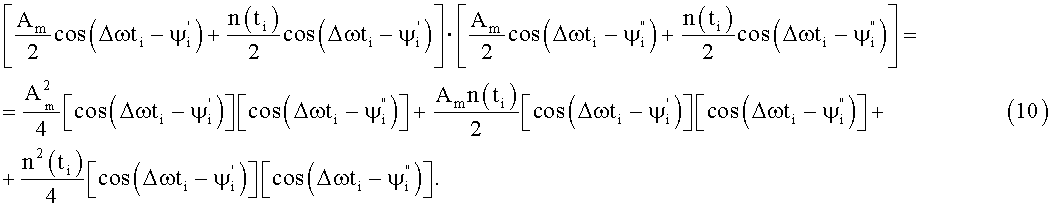
Сигналы (1) и (2) с выходов АЦП (9) и (14) в цифровой форме поступают на входы корреляторов (10) и (17) соответственно.Signals (1) and (2) from the outputs of the ADC (9) and (14) are digitally fed to the inputs of the correlators (10) and (17), respectively.
Работа схемы по установлению синхронизации по несущей и тактовой частотам. В корреляторе (10) (см. фиг.2) сигнал (1) поступает на его первый вход, который является первым входом П (33), а сигнал (2) - на его второй вход, который является первым входом П (31), а на третий вход Кр (10), который одновременно является вторыми входами П (33) и П (31), поступает сигнал ПСП, аналогичный ПСП, наложенной на сигнал меандра на передающей стороне. За счет квадратурной обработки сигналов в П (33) и (31) имеет место свертка ПСП, т.е. ее компенсация. С выходов П (33) и П (31) сигналы поступают на соответствующие входы ФВЧ (28) и ФВЧ (32), которые обеспечивают прохождение полезного сигнала и задерживают побочные продукты преобразования, в результате чего на выходе ФВЧ (28) сигнал (1) будет иметь видThe work of the scheme to establish synchronization on the carrier and clock frequencies. In the correlator (10) (see Fig. 2), the signal (1) goes to its first input, which is the first input P (33), and the signal (2) to its second input, which is the first input P (31) and the third input Кр (10), which is simultaneously the second inputs П (33) and П (31), receives the SRP signal, similar to the SRP superimposed on the meander signal on the transmitting side. Due to the quadrature signal processing, in PS (33) and (31) there is a convolution of the PSP, i.e. her compensation. From the outputs P (33) and P (31), the signals are fed to the corresponding inputs of the HPF (28) and HPF (32), which ensure the passage of the useful signal and delay the by-products of the conversion, resulting in the output of the HPF (28) signal (1) will have the form
![]()
![]()
а на выходе ФВЧ (32) сигнал (2) будет иметь видand at the output of the HPF (32), the signal (2) will have the form
![]()
![]()
где ![]()
![]()
Сигнал (3) с выхода ФВЧ (28) поступает на первый вход П (29) и на первый выход Кр (10), а сигнал (4) с выхода ФВЧ (32) - на второй вход П (29) и на второй выход Кр (10). В результате перемножения в П (29) происходит свертка меандра, а также появляется сигнал, который несет информацию о величине рассогласования ωн и ωуг The signal (3) from the output of the HPF (28) goes to the first input P (29) and to the first output Kr (10), and the signal (4) from the output of the HPF (32) goes to the second input P (29) and to the second output Cr (10). As a result of multiplication in P (29), the meander is convolved, and a signal appears that carries information about the mismatch value of ω n and ω y

Учитывая, что 2sinµ·cosν=sin(µ+ν)+sin(µ-ν) [3, стр.208], a ![]()
![]()
![]()
![]()

Сигнал (6) с выхода П (29) подается на вход ФНЧ (30), который обеспечивает усреднение входного сигнала. Тогда на выходе ФНЧ (30) появится сигнал видаThe signal (6) from the output P (29) is fed to the input of the low-pass filter (30), which provides averaging of the input signal. Then, at the output of the low-pass filter (30), a signal of the form

Поскольку ![]()
![]()
![]()
![]()

где ![]()
![]()
Рш=σ2 - мощность помехи.R W = σ 2 - power interference.
Из анализа выражения (7) следует, что на третьем выходе коррелятора (10) присутствует вторая гармоника разности частот ωн и ωуг, т.е. 2Δω, которая несет информацию о величине и знаке рассогласования несущей частоты и частоты управляемого генератора.From the analysis of expression (7) it follows that at the third output of correlator (10) there is a second harmonic of the frequency difference ω n and ω y , i.e. 2Δω, which carries information about the magnitude and sign of the mismatch of the carrier frequency and the frequency of the controlled generator.
Работа схемы по обеспечению синхронизации по несущей частоте. Сигнал вида (7) с выхода 3 коррелятора (10) подается на вход 2 УЦО (11) непосредственно, а через ЦАП (27) - на вход частотного дискриминатора (15) и на второй вход фазового детектора (5). На первый вход ФД (5) подается сигнал от ОГ (6) с частотой ωог. The work of the scheme to ensure synchronization of the carrier frequency. A signal of the form (7) from the output 3 of the correlator (10) is fed directly to the
а) Работа схемы при малых частотных расстройках. При малых частотных расстройках расхождение частот ωн и ωуг не превышает значений ![]()
![]()
б) Работа схемы при больших частотных расстройках. Большие частотные расстройки - это расстройки, при которых значение ![]()
![]()
Частотный дискриминатор на основе сигнала, поступившего на его вход, на своем выходе формирует сигнал положительной (если fн>fyг) или отрицательной (если fн<fyг) полярности. Знак полярности фиксируется компаратором (16) и с выхода К (16) подается на первый вход УЦО (11).A frequency discriminator based on the signal received at its input generates a signal of positive (if f n > f yg ) or negative (if f n <f yg ) polarity at its output. The polarity sign is fixed by the comparator (16) and from the output K (16) is fed to the first input of the UCO (11).
УЦО (11) выполняет функцию спектроанализатора на основе алгоритма быстрого преобразования Фурье (т.е. реализует гребенку узкополосных фильтров в диапазоне частот от (foг-2Δf) до (fог+2Δf), где 2Δf - максимальное значение величины абсолютной нестабильности генераторов передатчика и приемника по второй гармонике разности частот fн и fyг (см. выражение 7), с полосой пропускания каждого фильтра Δfфг, величина которой определяется требованиями к разрешающей способности и точности спектрального анализа) [4]. Сигнал, поступивший на второй вход УЦО (11), выделяется одним из фильтров гребенки. Появление сигнала на выходе соответствующего фильтра гребенки говорит о величине рассогласования fн и fуг. На основе информации о величине и знаке рассогласования на выходе УЦО (11) появляется управляющий сигнал, который поступает на второй вход УГ (2) и подстраивает его частоту в соответствии с принятой несущей («грубая» настройка), что приводит к уменьшению частотной расстройки генераторов передатчика и приемника. «Грубая» настройка позволяет установить значение ![]()
![]()
Работа схемы по обеспечению синхронизации по тактовой частоте ПСП.The operation of the scheme to ensure synchronization at the clock frequency of the memory bandwidth.
Сначала рассмотрим работу схемы при условии, что принятая ПСП и ПСП, выработанная генератором ПСП (18) приемника, совпадают. В корреляторе (17) (см. фиг.2) сигнал (1) поступает на его первый вход, который является первым входом П (27), а сигнал (2) - на его второй вход, который является первым входом П (31). На третий вход Кр (17), который одновременно является вторыми входами П (27) и П (31), поступает сигнал с выхода См2 (22). Этот сигнал является результатом сложения по модулю два двух сигналов (см фиг.3в): сигнала ПСП (см. фиг.3а), который подается с выхода ГенПСП (18) на первый вход См2 (22), и сигнала тактовой частоты ПСП (см. фиг.3б), который подается на второй вход См2 (22) с выхода УТГ (19). За счет квадратурной обработки сигналов в П (27) и в П (31) имеет место свертка ПСП, т.е. ее компенсация. С выходов П (27) и П (31) сигналы поступают на соответствующие входы ФВЧ (28) и ФВЧ (32), которые обеспечивают похождение полезного сигнала и задерживают побочные продукты преобразования, в результате чего на выходе ФВЧ (28) сигнал (1) будет иметь видFirst, we consider the operation of the circuit provided that the received SRP and the SRP generated by the receiver SRP (18) generator are the same. In the correlator (17) (see Fig. 2), the signal (1) goes to its first input, which is the first input P (27), and the signal (2) to its second input, which is the first input P (31) . The third input Kr (17), which is simultaneously the second inputs P (27) and P (31), receives a signal from the output of Sm2 (22). This signal is the result of modulo addition of two two signals (see Fig. 3c): the SRP signal (see Fig. 3a), which is fed from the output of the GenPSS (18) to the first input Sm2 (22), and the clock frequency signal of the SRP (see Fig.3b), which is fed to the second input of Sm2 (22) from the output of the UTG (19). Due to the quadrature signal processing in P (27) and P (31), there is a convolution of the PSP, i.e. her compensation. From the outputs P (27) and P (31), the signals are fed to the corresponding inputs of the HPF (28) and HPF (32), which provide a useful signal and delay the by-products of the conversion, resulting in the output of the HPF (28) signal (1) will have the form
![]()
![]()
а на выходе ФВЧ (32) сигнал (2) будет иметь видand at the output of the HPF (32), the signal (2) will have the form
![]()
![]()
где ![]()
![]()
γ - коэффициент, принимающий значения 0 или 1 в соответствии с последовательностью импульсов, поступающих на третий вход Кр (17) (см. фиг.3в).γ is a
Сигнал (8) с выхода ФВЧ (28) поступает на первый выход Кр (17), а сигнал (9) с выхода ФВЧ (32) - на второй выход Кр (17). В Кр (17) третий выход не используется.The signal (8) from the output of the HPF (28) goes to the first output of Kr (17), and the signal (9) from the output of the HPF (32) goes to the second output of Kr (17). In Kr (17), the third output is not used.
Сигнал (3) с первого выхода Кр (10) поступает на первый вход П (20), а сигнал (8) с первого выхода Кр (17) - на второй вход П (20). В результате перемножения на выходе П (20) появится сигнал видаThe signal (3) from the first output Kr (10) is supplied to the first input P (20), and the signal (8) from the first output Kr (17) is sent to the second input P (20). As a result of multiplication at the output P (20), a signal of the form
Учитывая, что 2cosµ·cosν=cos(µ+ν)+cos(µ-ν); ![]()
![]()
![]()
![]()

где ![]()
![]()
Поскольку ![]()
![]()
![]()
![]()
![]()
![]()

Сигнал (12) с выхода П (20) подается на вход ФНЧ (21), который подавляет сигнал с частотой 2Δωti и обеспечивает усреднение оставшейся части входного сигнала. Тогда, принимая во внимание, что ![]()
![]()
![]()
![]()

Одновременно сигнал (4) с второго выхода Кр (10) поступает на первый вход П (23), а сигнал (9) с второго выхода Кр (17) - на второй вход П (23). В результате перемножения на выходе П (23) появится сигнал видаAt the same time, signal (4) from the second output of Kr (10) goes to the first input of P (23), and signal (9) from the second output of Kr (17) goes to the second input of P (23). As a result of multiplication at the output P (23), a signal of the form

Учитывая, что 2sinµ·sinν=cos(µ-ν)-cos(µ+ν); ![]()
![]()
![]()
![]()
![]()
![]()
![]()
![]()

где ![]()
![]()
Сигнал (15) с выхода П (23) подается на вход ФНЧ (24), который подавляет сигнал с частотой 2Δωti и обеспечивает усреднение оставшейся части входного сигнала. Тогда, принимая во внимание, что ![]()
![]()
![]()
![]()

Сигнал (13) с выхода ФНЧ (21) поступает на первый вход Сум (25), а сигнал (16) с выхода ФНЧ (24) - на второй вход Сум (25). Анализ выражений (13) и (16) показывает, что на первый и второй входы Сум (25) поступает последовательность разнополярных импульсов (см. фиг.3г). Причем из правила формирования псевдослучайной последовательности известно, что в ней содержится приблизительно одинаковое число элементов (единиц и нулей) [5]. Следовательно, на выходе Сум (25) суммарное значение сигнала на интервале длительности ПСП будет приблизительно равно нулю, а это значит, что и на выходе ФСЗ (26) будет нулевой сигнал, что говорит о согласованности принятой и сформированной генератором ПСП (18) псевдослучайных последовательностей.The signal (13) from the output of the low-pass filter (21) goes to the first input of Sum (25), and the signal (16) from the output of the low-pass filter (24) goes to the second input of Sum (25). An analysis of expressions (13) and (16) shows that the sequence of bipolar pulses arrives at the first and second inputs of Sum (25) (see Fig. 3d). Moreover, it is known from the rule for the formation of a pseudo-random sequence that it contains approximately the same number of elements (ones and zeros) [5]. Therefore, at the output of Sum (25), the total value of the signal in the interval of the PSP duration will be approximately equal to zero, which means that at the output of the FSB (26) there will be a zero signal, which indicates the consistency of the pseudo-random sequences received and generated by the PSP generator (18) .
В случае несовпадения принятой и сформированной генератором ПСП (18) псевдослучайных последовательностей выражения (13) и (16) будут иметь видIn case of discrepancy between the pseudo-random sequences accepted and generated by the PSP generator (18), expressions (13) and (16) will have the form

![]()
![]()
Тогда в последовательности разнополярных импульсов, поступающих на первый и второй входы Сум (25), число положительных импульсов будет отличаться от числа отрицательных импульсов и на выходе Сум (25) суммарное значение сигнала на интервале длительности ПСП будет отлично от нуля. Причем величина этого сигнала пропорциональна величине рассогласования принятой и сформированной ГенПСП (18) последовательностей, а знак сигнала определяется задержкой или опережением принятой ПСП относительно опорной, сформированной ГенПСП (18). После предварительной фильтрации в ФСЗ (26) этот сигнал поступает на управляемый тактовый генератор (19) и обеспечивает устранение ошибки рассогласования ПСП по задержке.Then, in the sequence of unipolar pulses arriving at the first and second inputs of Sum (25), the number of positive pulses will differ from the number of negative pulses and at the output Sum (25) the total value of the signal in the interval of the PSP duration will be nonzero. Moreover, the magnitude of this signal is proportional to the discrepancy between the received and generated GenSSP (18) sequences, and the sign of the signal is determined by the delay or advancing of the received SSP relative to the reference formed by the GenSSP (18). After preliminary filtering in the FSZ (26), this signal is fed to a controlled clock generator (19) and ensures the elimination of the error in the mismatch of the SRP delay.
Оценка эффективности предложенного технического решения на этапе вхождения в синхронизмEvaluation of the effectiveness of the proposed technical solution at the stage of entry into synchronism
Из изложенного выше следует, что предложенное техническое решение (приемник) устойчиво обеспечивает начальную синхронизацию (т.е. захват сигнала схемой ФАПЧ) за счет оценки начальной расстройки частот принятой несущей и управляемого генератора (2) элементами устройства (частотным дискриминатором (15) и устройством цифровой обработки (11), которые способны эффективно работать при меньших значениях отношения сигнал/шум, чем схема ФАПЧ) и при параллельной работе схемы ФАПЧ. Действительно, процедура определения знака расстройки - двузначная операция, не требующая большого значения отношения сигнал/шум. Эффективность же работы УЦО (11) определяется, с одной стороны, максимальным значением начальной частотной расстройки (диапазоном неопределенности частотной расстройки), а с другой - дискретностью, т.е. максимально допустимой погрешностью измерения частоты, которая не должна превышать полосу захвата ФАПЧ, что также не требует больших отношений сигнал/шум. При успешной работе элементов дискретной коррекции начальной частотной расстройки и параллельной работе схемы ФАПЧ последней остается только свести к нулю остаточную расстройку несущей частоты, что не влечет за собой жестких требований на время устранения остаточной частотной расстройки частоты из-за переходных процессов в схеме ФАПЧ. Поскольку считается, что если сигнал попал в полосу захвата схемы ФАПЧ при отношении сигнал/шум на ее выходе ≥17 дБ, то считается, что синхронизация по несущей частоте установлена.From the above it follows that the proposed technical solution (receiver) stably provides initial synchronization (i.e., signal capture by the PLL) by evaluating the initial frequency detuning of the received carrier and the controlled oscillator (2) by the elements of the device (frequency discriminator (15) and the device digital processing (11), which are able to work efficiently at lower signal-to-noise ratios than the PLL) and with parallel operation of the PLL. Indeed, the procedure for determining the sign of a detuning is a two-digit operation that does not require a large signal-to-noise ratio. The efficiency of the UCO operation (11) is determined, on the one hand, by the maximum value of the initial frequency detuning (the range of uncertainty of the frequency detuning), and on the other hand, by discreteness, i.e. the maximum permissible error in measuring the frequency, which should not exceed the PLL capture band, which also does not require large signal-to-noise ratios. With the successful operation of the elements of discrete correction of the initial frequency detuning and the parallel operation of the PLL, the only thing left to do is to reduce the residual detuning of the carrier frequency to zero, which does not entail strict requirements for the time to eliminate the residual frequency detuning due to transients in the PLL. Since it is believed that if the signal fell into the PLL circuit capture band at a signal-to-noise ratio at its output of ≥17 dB, it is believed that the carrier frequency synchronization is established.
Оценим характеристики предложенного устройства при тех же начальных параметрах, которые были приведены выше, а именно: ширина спектра входного широкополосного сигнала (ШПС) ΔFшпс=16,384 МГц; тактовая частота формирования сигнала Fт=7 кГц; время установления синхронизации по несущей частоте Tсч≤4 мс; относительная нестабильность частоты δ=10-7; несущая частота fн=14 ГГц; полоса пропускания ФАПЧ, обеспечивающая требуемое качество синхронизации (отношение с/ш на выходе ФАПЧ>17 дБ), составляет 250 Гц; полоса схватывания фазового детектора Δfсx=500 Гц. Поскольку в нашем случае на второй вход фазового детектора (5) подается вторая гармоника частот рассогласования несущей и управляемого генератора (2), то максимальный диапазон частот, характеризующих величину их рассогласования, будет составлять 2·Δf=2·(2,8)=5,6 кГц, где Δf - максимальный диапазон нестабильности несущей частоты. Следовательно, интервал обработки УЦО (11) по частоте Fобр должен быть не менее 5,6 кГц.Let us evaluate the characteristics of the proposed device with the same initial parameters that were given above, namely: the width of the spectrum of the input broadband signal (BSS) ΔF bps = 16.384 MHz; the clock frequency of the signal formation F t = 7 kHz; carrier synchronization establishment time T sc ≤4 ms; relative frequency instability δ = 10 -7 ; carrier frequency f n = 14 GHz; the PLL bandwidth providing the required synchronization quality (s / w ratio at the PLL output> 17 dB) is 250 Hz; setting band of the phase detector Δf сx = 500 Hz. Since in our case, the second harmonic of the carrier mismatch frequencies and the controlled generator (2) is supplied to the second input of the phase detector (5), the maximum frequency range characterizing the size of their mismatch will be 2 · Δf = 2 · (2.8) = 5 , 6 kHz, where Δf is the maximum range of instability of the carrier frequency. Therefore, the processing interval of the UCO (11) in frequency F arr should be at least 5.6 kHz.
Согласно [4] максимальный интервал обработки по частоте Foбp max при использовании квадратурной обработки определяется частотой дискретизации fд, т.е. Foбр max=fд. Поскольку ширина спектра сигнала ΔFшпс=16,384 МГц, то частота дискретизации fд, как минимум, в два раза выше спектра сигнала и значительно выше требуемого интервала обработки Fобр УЦО (11), что позволяет использовать УЦО в качестве спектроанализатора, представляющего собой гребенку узкополосных фильтров с полосой пропускания каждого фильтра Δfфг. According to [4], the maximum processing interval in frequency F about max when using quadrature processing is determined by the sampling frequency f d , ie F about max = f d. Since the signal spectrum width is ΔF bds = 16.384 MHz, the sampling frequency f d is at least two times higher than the signal spectrum and significantly higher than the required processing interval F arr UCO (11), which allows the use of UCO in as a spectrum analyzer, which is a comb of narrow-band filters with a passband of each filter Δf fg.
Чтобы в результате «грубой» подстройки величина рассогласования не превысила полосу захвата ФАПЧ, полоса пропускания каждого фильтра Δfфг должна быть ≤500 Гц. Тогда весь диапазон частотной расстройки должен быть разбит на 5600/500=11,2≈12 частей, т.е. устройство цифровой обработки должно включать 12 фильтров с полосой пропускания ≈466 Гц.So that as a result of a “rough” adjustment, the mismatch does not exceed the PLL capture bandwidth, the passband of each filter Δf fg should be ≤500 Hz. Then the entire range of frequency detuning should be divided into 5600/500 = 11.2≈12 parts, i.e. The digital processing device should include 12 filters with a passband of ≈466 Hz.
Известно [6], что при реализации функции спектроанализа на основе алгоритма быстрого преобразования Фурье необходимое число фильтров m определяется выражением 2n, где n принимает значения 1, 2, 3, … . Для нашего случая n=4, а m=16. Значит УЦО (11) будет содержать 16 фильтров, каждый из которых имеет полосу пропускания Δfфг=350 Гц, что позволяет оценить длительность интервала оценивания УЦО, который составляетIt is known [6] that, when implementing the spectrum analysis function based on the fast Fourier transform algorithm, the required number of filters m is determined by the
![]()
![]()
При этом отношение сигнал/шум на выходе УЦО будетIn this case, the signal-to-noise ratio at the output of the UCO will be

что вполне достаточно для однозначной оценки величины и знака частотной расстройки.which is quite sufficient for an unambiguous assessment of the magnitude and sign of the frequency detuning.
Таким образом, предложенное техническое решение по синхронизации приемных устройств по несущей и тактовой частотам в системах с кодовым разделением каналов в условиях большой нестабильности частот в канале связи обеспечивает решение задачи синхронизации с высокой надежностью и за время до 4 мс.Thus, the proposed technical solution for synchronizing receiving devices by carrier and clock frequencies in systems with code division multiplexing under conditions of great frequency instability in the communication channel provides a solution to the synchronization problem with high reliability and for up to 4 ms.
ЛитератураLiterature
1. Новые стандарты широкополосной радиосвязи на базе технологии W-CDMA, М.: Международный центр научно-технической информации, 1999 (стр.38-58).1. New standards for broadband radio communications based on W-CDMA technology, M .: International Center for Scientific and Technical Information, 1999 (pp. 38-58).
2. Алексеев А.И., Шереметьев А.Г., Тузов Г.И., Глазов Б.И. Теория и применение псевдослучайных сигналов. - М.: Наука, 1969. - 367 с.2. Alekseev A.I., Sheremetyev A.G., Tuzov G.I., Glazov B.I. Theory and application of pseudo-random signals. - M .: Nauka, 1969 .-- 367 p.
3. Рывкин А.А., Рывкин А.З., Хренов Л.С. Справочник по математике. Изд. 3-е, стереотип. М.: Высшая школа, 1975. - 554 с.3. Ryvkin A.A., Ryvkin A.Z., Khrenov L.S. Math reference. Ed. 3rd, stereotype. M .: Higher School, 1975 .-- 554 p.
4. Цифровые фильтры и устройства обработки сигналов на интегральных микросхемах: Справочное пособие / Ф.Б.Высоцкий, В.И.Алексеев, В.Н.Пачин и др. Под ред. Б.Ф.Высоцкого. М.: Радио и связь, 1984. - 216 с.4. Digital filters and signal processing devices on integrated circuits: Reference manual / FB Vysotsky, V.I. Alekseev, V.N. Pachin and others. Ed. B.F. Vysotsky. M .: Radio and communications, 1984. - 216 p.
5. Шумоподобные сигналы в системах передачи информации. Под ред. проф. В.Б.Пестрякова. М.: Сов. радио, 1973, с.424 (с.115).5. Noise-like signals in information transmission systems. Ed. prof. V. B. Pestryakova. M .: Sov. Radio, 1973, p. 424 (p. 115).
6. Введение в цифровую фильтрацию. Под ред. Р.Боргера и А.Констандинидиса. Пер. с англ. под ред. Л.И.Филиппова. - М.: Мир, 1976. - 216 с.6. Introduction to digital filtering. Ed. R. Borger and A. Konstandinidis. Per. from English under the editorship of L.I. Filippova. - M .: Mir, 1976 .-- 216 p.
Claims (1)
Priority Applications (1)
| Application Number | Priority Date | Filing Date | Title |
|---|---|---|---|
| RU2011101750/08A RU2450446C1 (en) | 2011-01-19 | 2011-01-19 | Device to synchronise receiving devices by carrier and clock frequencies in systems with code division of channels under high instability of frequencies in communication channel |
Applications Claiming Priority (1)
| Application Number | Priority Date | Filing Date | Title |
|---|---|---|---|
| RU2011101750/08A RU2450446C1 (en) | 2011-01-19 | 2011-01-19 | Device to synchronise receiving devices by carrier and clock frequencies in systems with code division of channels under high instability of frequencies in communication channel |
Publications (1)
| Publication Number | Publication Date |
|---|---|
| RU2450446C1 true RU2450446C1 (en) | 2012-05-10 |
Family
ID=46312452
Family Applications (1)
| Application Number | Title | Priority Date | Filing Date |
|---|---|---|---|
| RU2011101750/08A RU2450446C1 (en) | 2011-01-19 | 2011-01-19 | Device to synchronise receiving devices by carrier and clock frequencies in systems with code division of channels under high instability of frequencies in communication channel |
Country Status (1)
| Country | Link |
|---|---|
| RU (1) | RU2450446C1 (en) |
Cited By (3)
| Publication number | Priority date | Publication date | Assignee | Title |
|---|---|---|---|---|
| RU2535198C1 (en) * | 2013-10-03 | 2014-12-10 | Открытое акционерное общество "Концерн "Созвездие" | Method and device for reference signal generation by computers in systems of frequency and phase synchronisation of broadband communication systems |
| WO2015041566A1 (en) * | 2013-09-23 | 2015-03-26 | Llc "Topcon Positioning Systems" | Apparatus for correcting multipath errors in carrier phase measurements of a navigation receiver |
| US9385767B2 (en) | 2013-05-28 | 2016-07-05 | Topcon Positioning Systems, Inc. | Apparatus for correcting multipath errors in carrier phase measurements of a navigation receiver |
Citations (6)
| Publication number | Priority date | Publication date | Assignee | Title |
|---|---|---|---|---|
| SU751295A1 (en) * | 1978-03-02 | 1986-07-30 | Предприятие П/Я А-7287 | Tracking receiver of pseudorandom signals |
| RU2246181C2 (en) * | 2002-11-14 | 2005-02-10 | Военная академия Ракетных войск стратегического назначения им. Петра Великого | Receiver for quadratic-modified signals with displacement for multichannel communications system with coded channel separation |
| EP1658680B1 (en) * | 2003-07-18 | 2007-01-17 | Artimi Ltd | Communications systems and methods |
| EP1656743B1 (en) * | 2003-07-18 | 2007-01-17 | Artimi Ltd | Communications systems and methods |
| EP1647098B1 (en) * | 2003-07-18 | 2007-02-21 | Artimi Ltd | UWB receiver system with RF analog to digital conversion (ADC) before the correlation |
| SU1840438A1 (en) * | 1978-12-13 | 2007-03-10 | Воронежский научно-исследовательский институт связи | Device for automatically finding radio communication channels for adaptive address systems |
-
2011
- 2011-01-19 RU RU2011101750/08A patent/RU2450446C1/en not_active IP Right Cessation
Patent Citations (6)
| Publication number | Priority date | Publication date | Assignee | Title |
|---|---|---|---|---|
| SU751295A1 (en) * | 1978-03-02 | 1986-07-30 | Предприятие П/Я А-7287 | Tracking receiver of pseudorandom signals |
| SU1840438A1 (en) * | 1978-12-13 | 2007-03-10 | Воронежский научно-исследовательский институт связи | Device for automatically finding radio communication channels for adaptive address systems |
| RU2246181C2 (en) * | 2002-11-14 | 2005-02-10 | Военная академия Ракетных войск стратегического назначения им. Петра Великого | Receiver for quadratic-modified signals with displacement for multichannel communications system with coded channel separation |
| EP1658680B1 (en) * | 2003-07-18 | 2007-01-17 | Artimi Ltd | Communications systems and methods |
| EP1656743B1 (en) * | 2003-07-18 | 2007-01-17 | Artimi Ltd | Communications systems and methods |
| EP1647098B1 (en) * | 2003-07-18 | 2007-02-21 | Artimi Ltd | UWB receiver system with RF analog to digital conversion (ADC) before the correlation |
Cited By (3)
| Publication number | Priority date | Publication date | Assignee | Title |
|---|---|---|---|---|
| US9385767B2 (en) | 2013-05-28 | 2016-07-05 | Topcon Positioning Systems, Inc. | Apparatus for correcting multipath errors in carrier phase measurements of a navigation receiver |
| WO2015041566A1 (en) * | 2013-09-23 | 2015-03-26 | Llc "Topcon Positioning Systems" | Apparatus for correcting multipath errors in carrier phase measurements of a navigation receiver |
| RU2535198C1 (en) * | 2013-10-03 | 2014-12-10 | Открытое акционерное общество "Концерн "Созвездие" | Method and device for reference signal generation by computers in systems of frequency and phase synchronisation of broadband communication systems |
Similar Documents
| Publication | Publication Date | Title |
|---|---|---|
| JP4194759B2 (en) | System and method for narrowing the frequency uncertainty range of a Doppler shifted signal | |
| CN111989877B (en) | Apparatus and receiver for performing synchronization in analog spread spectrum system | |
| AU8157898A (en) | Receiving a spread spectrum signal | |
| US20070110126A1 (en) | Radio communication system and communication apparatus | |
| CA2947106A1 (en) | Method and measuring device for intermodulation measurement | |
| EP2860876A1 (en) | Local oscillator phase noise compensation | |
| RU2450446C1 (en) | Device to synchronise receiving devices by carrier and clock frequencies in systems with code division of channels under high instability of frequencies in communication channel | |
| EP0560071A2 (en) | Method of signalling | |
| RU2451408C2 (en) | Apparatus for synchronising carrier and reference frequency in communication channel with considerable frequency instabilities and energy constraints | |
| US8009723B2 (en) | Measurement of baseband timing in a spread spectrum communications system | |
| Boscagli et al. | PN regenerative ranging and its compatibility with telecommand and telemetry signals | |
| Naeem et al. | Doppler shift compensation techniques for LEO satellite on-board receivers | |
| JP4114687B2 (en) | Multi-rate clock signal extraction method and multi-rate clock signal extraction device | |
| US9484969B2 (en) | Delta-pi signal acquisition | |
| US9484968B2 (en) | Post conversion mixing | |
| RU2254679C1 (en) | Coherent receiver of modulated signals with a shift of multi-channel communication system (oqpsk) with code separation of channels | |
| CN114323072B (en) | Dual-channel combined zero value real-time calibration device and method | |
| Friedt et al. | Development of an opensource, openhardware, software-defined radio platform for two-way satellite time and frequency transfer | |
| RU2336634C1 (en) | Device for transmission and reception of phase- and frequency-shift broadband signals for mobil objects equipped with radio burst control line locks | |
| RU2276459C1 (en) | Quasi-optimal receiver of discontinuous-continuous phase-manipulated signals | |
| RU2811900C1 (en) | Method for energy detection of signal with compensation of combinational components under conditions of exposure to non-stationary interference | |
| RU2246181C2 (en) | Receiver for quadratic-modified signals with displacement for multichannel communications system with coded channel separation | |
| EP2909942A1 (en) | Periodic time segment sequence based signal generation | |
| RU2115236C1 (en) | Communication system with wide-band signals | |
| RU2733261C1 (en) | Multichannel receiver with coherent frequency-code division of channels for reception of quadrature-modulated signals of higher structural security |
Legal Events
| Date | Code | Title | Description |
|---|---|---|---|
| MM4A | The patent is invalid due to non-payment of fees |
Effective date: 20130120 |