RU2444059C2 - Integrated device and method of reading images - Google Patents
Integrated device and method of reading images Download PDFInfo
- Publication number
- RU2444059C2 RU2444059C2 RU2008102837/08A RU2008102837A RU2444059C2 RU 2444059 C2 RU2444059 C2 RU 2444059C2 RU 2008102837/08 A RU2008102837/08 A RU 2008102837/08A RU 2008102837 A RU2008102837 A RU 2008102837A RU 2444059 C2 RU2444059 C2 RU 2444059C2
- Authority
- RU
- Russia
- Prior art keywords
- substrate
- image
- configuration
- trained
- many
- Prior art date
Links
Images


Classifications
-
- G—PHYSICS
- G06—COMPUTING OR CALCULATING; COUNTING
- G06V—IMAGE OR VIDEO RECOGNITION OR UNDERSTANDING
- G06V10/00—Arrangements for image or video recognition or understanding
- G06V10/94—Hardware or software architectures specially adapted for image or video understanding
-
- H—ELECTRICITY
- H04—ELECTRIC COMMUNICATION TECHNIQUE
- H04N—PICTORIAL COMMUNICATION, e.g. TELEVISION
- H04N25/00—Circuitry of solid-state image sensors [SSIS]; Control thereof
-
- G—PHYSICS
- G06—COMPUTING OR CALCULATING; COUNTING
- G06V—IMAGE OR VIDEO RECOGNITION OR UNDERSTANDING
- G06V10/00—Arrangements for image or video recognition or understanding
- G06V10/10—Image acquisition
Landscapes
- Engineering & Computer Science (AREA)
- Multimedia (AREA)
- Physics & Mathematics (AREA)
- General Physics & Mathematics (AREA)
- Theoretical Computer Science (AREA)
- Software Systems (AREA)
- Signal Processing (AREA)
- Solid State Image Pick-Up Elements (AREA)
- Image Analysis (AREA)
- Transforming Light Signals Into Electric Signals (AREA)
Abstract
Description
Ссылки на связанные заявки:Links to related applications:
Настоящая заявка претендует на приоритет предварительной патентной заявки US 60/694988, поданной 30 июня 2005 г., содержание которой полностью включено в настоящее описание посредством ссылки.This application claims the priority of provisional patent application US 60/694988, filed June 30, 2005, the contents of which are fully incorporated into this description by reference.
Предпосылки создания изобретенияBACKGROUND OF THE INVENTION
Область техникиTechnical field
В целом изобретение относится к области устройств для формирования изображений. В частности, настоящее изобретение относится к микроустройствам для распознавания образов (изображений), расположенным на прозрачной подложке, например стекле, или встроенным в нее.In general, the invention relates to the field of imaging devices. In particular, the present invention relates to microdevices for pattern recognition (images) located on a transparent substrate, such as glass, or integrated into it.
Уровень техникиState of the art
Прозрачные поверхности, например стеклянные, существовали сотни лет. Прозрачные поверхности первоначально использовались для защиты жилого пространства, позволяя его обитателям воспринимать окружающий мир (местность, погода и возможные опасности). В последнее время на прозрачные поверхности существует огромная потребность для производства дисплеев, начиная от электронно-лучевых трубок (ЭЛТ) и кончая, в последние годы, жидкокристаллическими дисплеями (ЖК-дисплеи) и разного рода дисплеями с плоскими панелями. При их использовании, во многих случаях человек или живые организмы (животные, растения) располагаются вблизи таких прозрачных поверхностей.Transparent surfaces, such as glass, have existed for hundreds of years. Transparent surfaces were originally used to protect the living space, allowing its inhabitants to perceive the surrounding world (terrain, weather and possible dangers). Recently, there has been a huge need for transparent displays on transparent surfaces, ranging from cathode ray tubes (CRTs) to, in recent years, liquid crystal displays (LCDs) and all kinds of flat panel displays. When used, in many cases a person or living organisms (animals, plants) are located near such transparent surfaces.
Датчики изображения используются уже несколько десятилетий (например, ПЗС датчики (датчики на базе приборов с зарядовыми связями) или КМОП датчики (датчики на комплементарных структурах "металл/оксид/полупроводник"). Например, в US 6617565, содержание которого включено в настоящее описание посредством ссылки, описан КМОП датчик изображения на одном кристалле. Типовыми конструкциями датчиков изображения являются камеры, включающие установленную за линзой объектива интегральную схему, которая может быть миниатюрной или сменной (например, навинчивающаяся линза). Чувствительные элементы датчика предназначены для преобразования световой энергии (фотоны) в электрический сигнал, пропорциональный количеству света, принятому фоточувствительными элементами, из которых в чувствительном элементе датчика сформирована решетка. Изображение синтезируется из выходных сигналов фоточувствительных элементов.Image sensors have been used for several decades (for example, CCD sensors (sensors based on charge-coupled devices) or CMOS sensors (sensors on complementary metal / oxide / semiconductor structures). For example, in US 6617565, the contents of which are incorporated into this description by links, described CMOS image sensor on a single crystal.Typical designs of image sensors are cameras, including an integrated circuit installed behind the lens of the lens, which can be miniature or interchangeable (for example, nav nchivayuschayasya lens). The sensing elements of the sensor are used to convert light energy (photons) into an electrical signal proportional to the amount of light received by the photosensitive elements, of which in the sensitive sensor element is formed lattice. The image synthesized from the outputs of the photosensitive elements.
Технологии распознавания образов становятся все более востребованными. Видеокамеры различных размеров и конструкций требуются для самых различных применений, например охраны, идентификации личности, разведки, контроля качества, наблюдения за дорожным движением и др. Видеокамеры часто соединены с дисплеями либо проводной, либо беспроводной связью. Сегодня видеокамеры, объединенные с ЖК-дисплеем, стали стандартной принадлежностью сотовых телефонов.Pattern recognition technologies are becoming more and more popular. Video cameras of various sizes and designs are required for a wide variety of applications, such as security, identification, reconnaissance, quality control, traffic monitoring, etc. Video cameras are often connected to displays either by wire or wireless. Today, camcorders combined with an LCD display have become a standard accessory for cell phones.
Для совершенствования распознавания образов требуется синтез изображения высокого разрешения. Существующие системы распознавания образов работают со сравнительно невысокой скоростью из-за низких вычислительных возможностей и/или из-за того, что процессоры могут вести обработку не более одного пиксела изображения за один раз.To improve pattern recognition, high-resolution image synthesis is required. Existing pattern recognition systems operate at a relatively low speed due to low computational capabilities and / or due to the fact that processors can process no more than one image pixel at a time.
Таким образом, требуется создание новых устройств распознавания образов, более совершенных, чем существующие.Thus, the creation of new pattern recognition devices that are more advanced than existing ones is required.
Краткое изложение сущности изобретенияSummary of the invention
В основу настоящего изобретения положена задача создания устройства для распознавания образов (изображений), имеющего чувствительную площадку (например, фоточувствительные элементы), непосредственно встроенную в прозрачный или полупрозрачный материал, образующий оптический интерфейс между падающим изображением и чувствительной площадкой. В предпочтительном варианте, само устройство распознавания образов является прозрачным или полупрозрачным.The present invention is based on the task of creating a device for pattern recognition (images) having a sensitive area (for example, photosensitive elements) directly integrated into a transparent or translucent material, forming an optical interface between the incident image and the sensitive area. In a preferred embodiment, the pattern recognition device itself is transparent or translucent.
Другой задачей настоящего изобретения является обеспечение чувствительной площадки, обладающей функцией самостоятельного ("на месте") принятия решения с использованием решетки обучаемых процессорных элементов. В одном варианте осуществления настоящего изобретения, обучаемые элементы когнитивной памяти или ячейки связаны с одним или более фоточувствительными элементами. Преимуществом принятия решения "на месте" является то, что снижаются требования к скорости передачи данных устройством (т.е. полосе), особенно в тех случаях, когда число фоточувствительных элементов велико, и должна быть высока частота передачи данных фоточувствительных элементов. Используя большие решетки чувствительных площадок, каждая из которых обладает способностью принятия решений "на месте", можно создать устройство формирования изображения с высоким быстродействием и разрешением.Another objective of the present invention is the provision of a sensitive site with the function of independent ("in place") decision making using a lattice of trained processor elements. In one embodiment of the present invention, learning elements of cognitive memory or cells are associated with one or more photosensitive elements. The advantage of making the decision “in place” is that the requirements for the data transfer speed of the device (ie, the band) are reduced, especially in cases where the number of photosensitive elements is large and the frequency of data transmission of photosensitive elements must be high. Using large lattices of sensitive areas, each of which has the ability to make decisions on the spot, you can create an image forming device with high speed and resolution.
В соответствии с вариантом осуществления настоящего изобретения, обучаемые элементы когнитивной памяти могут работать параллельно на низких частотах и потреблять очень малый ток. Как следствие, может обеспечиваться автономная работа каждого элемента при использовании маломощных источников энергии, например солнечных батарей или их эквивалентов.According to an embodiment of the present invention, the cognitive memory elements being trained can operate in parallel at low frequencies and consume very low current. As a result, the autonomous operation of each element can be ensured when using low-power sources of energy, such as solar panels or their equivalents.
В соответствии с вариантом осуществления настоящего изобретения, новое интегральное устройство распознавания образов образовано соединением одного или более фоточувствительных элементов с одним или более обучаемых элементов когнитивной памяти, причем все они встроены в подложку.According to an embodiment of the present invention, a new integrated pattern recognition device is formed by combining one or more photosensitive elements with one or more learnable cognitive memory elements, all of which are embedded in the substrate.
В соответствии с вариантом выполнения настоящего изобретения, множество фоточувствительных элементов, связанных с большим числом обучаемых элементов когнитивной памяти, может быть организовано в одну или несколько решеток и распределено по плоской прозрачной или полупрозрачной подложке. Решетки могут обладать изменяемыми геометрией и соединяемостью. К типичной геометрии относится линейная решетка параллельно расположенных нейронов, либо двумерная решетка нейронов, объединенных растровой или сотовой геометрией. Могут быть и иные конфигурации.According to an embodiment of the present invention, a plurality of photosensitive elements associated with a large number of learning elements of cognitive memory can be organized into one or more arrays and distributed on a flat transparent or translucent substrate. Lattices may have variable geometry and connectivity. Typical geometry is a linear lattice of parallel neurons, or a two-dimensional lattice of neurons connected by raster or cellular geometry. There may be other configurations.
Другие применения и преимущества различных вариантов осуществления настоящего изобретения рассматриваются ниже со ссылками на чертежи, иллюстрирующие эти варианты осуществления изобретения.Other applications and advantages of various embodiments of the present invention are discussed below with reference to the drawings illustrating these embodiments of the invention.
Краткое описание чертежейBrief Description of the Drawings
На фиг.1А-Б представлены, соответственно, вид спереди и вид сверху решеток чувствительных элементов, расположенных на стекле или плексигласе, или ином прозрачном пластике или прозрачной подложке, в которой гравированы линзы;On figa-B, respectively, is a front view and a top view of the gratings of sensitive elements located on glass or plexiglass, or other transparent plastic or a transparent substrate in which the lenses are engraved;
На фиг.2 представлен вид сверху решетки чувствительных элементов, расположенных на стеклянной или плексигласовой подложке с гравированными в ней линзами, в процессе распознавания фрагментов ДНК;Figure 2 presents a top view of the lattice of sensitive elements located on a glass or plexiglass substrate with engraved lenses in it, in the process of recognition of DNA fragments;
На фиг.3А-Б представлены, соответственно, вид сбоку и вид сверху матрицы чувствительных элементов;On figa-B presents, respectively, a side view and a top view of a matrix of sensitive elements;
На фиг.4 представлена блок-схема чувствительных элементов;Figure 4 presents a block diagram of the sensing elements;
На фиг.5А представлена блок-схема решеток чувствительных элементов;On figa presents a block diagram of the grids of the sensitive elements;
На фиг.5Б представлена блок-схема банка решеток чувствительных элементов;On figb presents a block diagram of a bank of lattices of sensitive elements;
На фиг.6А-В представлена конфигурация нейрона;6A-B show a configuration of a neuron;
На фиг.7 представлена блок-схема нейрона; и7 is a block diagram of a neuron; and
На фиг.8-12 приведены примеры применения устройства распознавания образов.On Fig-12 shows examples of application of the pattern recognition device.
Подробное описание предмета изобретенияDetailed description of the subject invention
Хотя настоящее изобретение может быть осуществлено во множестве различных форм, в данном раскрытии описано несколько предпочтительных вариантов осуществления, которые используются только в качестве иллюстрации принципов изобретения, поэтому изобретение не должно считаться ограниченным этими конкретными вариантами.Although the present invention can be implemented in many different forms, this disclosure describes several preferred embodiments that are used only to illustrate the principles of the invention, therefore, the invention should not be considered limited to these specific options.
Настоящее изобретение представляет собой формирователь изображения, который может включать чувствительное воспринимающее устройство, например фоточувствительный элемент, соединенный, скрепленный либо иначе связанный с обучаемым когнитивным элементом, причем оба элементы нанесены химическим или иным путем на поверхность прозрачной подложки, либо встроены в нее. Объединение чувствительной площадки с обучаемым когнитивным элементом, обладающим способностью принятия решения "на месте", в настоящем документе называется "CogniSensor" ("познающий чувствительный элемент"). Обучаемый когнитивный элемент в настоящем документе называется "CogniMem" ("познающая память"). Чувствительные площадки выполнены из одного или более фоточувствительных элементов, но могут быть и другие варианты конфигурации чувствительной области.The present invention is an imaging device, which may include a sensitive sensing device, for example a photosensitive element, connected, fastened or otherwise connected with a learner cognitive element, both elements being applied chemically or otherwise to the surface of the transparent substrate, or integrated into it. Combining a sensitive site with a learner-based cognitive element that has the ability to make decisions “in place” is referred to in this document as “CogniSensor” (“knowing sensitive element”). The learning cognitive element in this document is called "CogniMem" ("cognitive memory"). Sensitive areas are made of one or more photosensitive elements, but there may be other configuration options for the sensitive area.
В соответствии с вариантами осуществления настоящего изобретения, конфигурация CogniSensors может обеспечивать распознавание приходящей световой картины (например, изображений или частей изображений), обработку приходящей световой картины для принятия решения "на месте" и передачу результатов этого решения или его индикацию. CogniSensor может включать несколько компонентов, например логическую схему ввода данных для принятия решения "на месте", "нейроны" и логическую схему вывода решений, буфер памяти, солнечные элементы для обеспечения автономной работы, а также и другие компоненты. В предпочтительном варианте осуществления, каждый CogniSensor включает параллельно организованные элементы реагирующей обучаемой ассоциативной памяти (REALM). Согласно варианту осуществления изобретения, CogniMem обеспечивает распознавание образов, как аналоговое, так и цифровое, без подключения к компьютеру.In accordance with embodiments of the present invention, the CogniSensors configuration can provide recognition of an incoming light picture (eg, images or portions of images), processing the incoming light picture to make an in-place decision, and transmitting the results of this decision or indicating it. CogniSensor can include several components, for example, a logic diagram of data input for making decisions on the spot, "neurons" and a logic diagram of decision output, a memory buffer, solar cells to ensure autonomous operation, as well as other components. In a preferred embodiment, each CogniSensor includes parallel organized reactive learning associative memory (REALM) elements. According to an embodiment of the invention, CogniMem provides pattern recognition, both analog and digital, without connecting to a computer.
CogniMem может содержать один или более нейронов, которые представляют собой параллельно организованные элементы ассоциативной памяти, которые могут реагировать на входные образы, аналогичные их собственному контенту. Нейроны могут реагировать как индивидуально, так и коллективно, подкрепляя свою реакцию реакцией других соседних нейронов. Выбор может осуществляться по входной линии "торможение/возбуждение", подходящей к нейронам.CogniMem can contain one or more neurons, which are parallel organized elements of associative memory that can respond to input images similar to their own content. Neurons can respond both individually and collectively, reinforcing their reaction with the reaction of other neighboring neurons. The selection can be made on the input line "inhibition / excitation", suitable for neurons.
Контент нейронов CogniMem образует "знание". Знание представляет собой набор статистически разделяемых сигнатур. Знание может быть статическим (загружаемым однократно) или динамическим (обновляемым реакцией других нейронов или загружаемым адаптивно из внешней базы данных знания), а в предпочтительном варианте знание генерируется автоматически в процессе обучения без использования компьютера. CogniMem, располагающаяся на той же подложке, может использовать это же или какое-либо иное знание.The content of CogniMem neurons forms “knowledge.” Knowledge is a collection of statistically shared signatures. Knowledge can be static (downloaded once) or dynamic (updated by the reaction of other neurons or downloaded adaptively from an external knowledge database), and in the preferred embodiment, knowledge is generated automatically during training without using a computer. CogniMem, located on the same substrate, can use the same or some other knowledge.
CogniMem может быть нанесена или встроена (либо присоединена иным способом) к подложке, как часть CogniSensor, либо может быть отдельным компонентом. В первом случае, CogniMem обычно используется для распознавания данных пикселов, получаемых от фоточувствительного элемента. Во втором случае, CogniMem может быть использована для обслуживания других CogniMem и может, например, распознавать данные различных типов, передаваемые другими узлами CogniMem (например, для объединения образов по выходным данным с многих CogniSensors).CogniMem can be applied or embedded (or otherwise attached) to the substrate, as part of CogniSensor, or it can be a separate component. In the first case, CogniMem is usually used to recognize pixel data received from a photosensitive element. In the second case, CogniMem can be used to service other CogniMem and can, for example, recognize data of various types transmitted by other CogniMem nodes (for example, to combine images from many CogniSensors by output data).
Приведенные ниже патенты и опубликованные заявки, содержание которых полностью включено в настоящее раскрытие посредством ссылки, описывают различные особенности нейронов и нейронных сетей, применимые к CogniMems и CogniSensors: US 5621863 - Нейронная сеть; 5717832 - Усовершенствованная архитектура нейронной сети; 5701397 - Схема для предварительной загрузки свободной нейронной сети; 5710869 - Гирляндная схема для последовательного соединения нейронных сетей; 5740326 - Поиск/сортировка данных в нейронных сетях; 6332137 - Параллельная ассоциативная память для распознавания изолированного оборудования; 6606614 - Однопроводный поиск и сортировка; заявки Японии JP 8-171543 - Гирляндная схема для последовательного соединения нейронных сетей; JP 8-171542 - Усовершенствованная схема загрузки; JP 8171541 - Схема группирования (поиск/сортировка); JP 8-171540 - Нейронная сеть и нейронный чип; JP 8-069445 - Архитектура нейронной сети; патентная заявка Кореи KR 164943 - Новая архитектура нейронной сети; Европейские патенты ЕР 0694852 - Новая архитектура нейронной сети; ЕР 0694854 - Усовершенствованная нейронная архитектура полупроводникового чипа; ЕР 0694855 - Поиск/сортировка для нейронных сетей; ЕР 0694853 - Схема для предварительной загрузки компонентов входного вектора в сети свободных нейронов в фазе распознавания; ЕР 0694856 - Гирляндная схема для последовательного соединения нейронных сетей; заявка Канады СА 2149478 - Усовершенствованная архитектура нейронной сети; патент Канады СА 2149479 - Усовершенствованная нейронная архитектура полупроводникового чипа.The following patents and published applications, the contents of which are fully incorporated into this disclosure by reference, describe various features of neurons and neural networks applicable to CogniMems and CogniSensors: US 5621863 - Neural network; 5717832 - Advanced neural network architecture; 5701397 - Scheme for preloading a free neural network; 5710869 - Daisy chain for serial connection of neural networks; 5740326 - Search / sorting of data in neural networks; 6332137 - Parallel associative memory for recognition of isolated equipment; 6606614 - Single-wire search and sorting; Japanese application JP 8-171543 - Daisy chain for serial connection of neural networks; JP 8-171542 - Advanced loading scheme; JP 8171541 - Grouping scheme (search / sort); JP 8-171540 - Neural network and neural chip; JP 8-069445 - Neural Network Architecture; Korean Patent Application KR 164943 - New Neural Network Architecture; European Patents EP 0694852 - New Neural Network Architecture; EP 0694854 - Advanced neural architecture of a semiconductor chip; EP 0694855 - Search / Sort for Neural Networks; EP 0694853 - Scheme for preloading input vector components in a network of free neurons in the recognition phase; EP 0694856 - Daisy chain for serial connection of neural networks; Canadian application CA 2149478 - Advanced neural network architecture; Canadian Patent CA 2149479 - Advanced Neural Semiconductor Chip Architecture.
Число нейронов, реализованных на CogniMem, может составлять от 1 до N, где N теоретически неограниченно благодаря архитектуре нейронной ячейки. В настоящее время N может достигать 1000. Вообще, N зависит от применения и, в частности, от разнообразия образов, которые требуется распознавать, и типа решений, которые необходимо передавать. Специалисту должно быть понятно, что технология кремниевых приборов может быть фактором, определяющим количество нейронов на единицу площади.The number of neurons implemented on CogniMem can range from 1 to N, where N is theoretically unlimited due to the architecture of the neural cell. Currently, N can reach 1000. In general, N depends on the application and, in particular, on the variety of patterns that need to be recognized, and the type of solutions that need to be transmitted. The specialist should be clear that the technology of silicon devices can be a factor determining the number of neurons per unit area.
Пример конфигурации устройства распознавания образов, согласно варианту осуществления настоящего изобретения, показан на фиг.1А и 1Б. Фиг.1А представляет вид сверху устройства 100, которое включает подложку 102, которая может быть выполнена из ряда прозрачных или полупрозрачных материалов, например стекла, плексигласа, прозрачных пластиков и др. Один или более CogniSensors 104 (в данном случае, в виде решетки) может быть встроен в подложку 102 или, как в данном случае, прикреплен или приклеен, либо как-то иначе связан с поверхностью подложки 102 (см. фиг.1Б). Оптический тракт может быть гравирован или нанесен на подложку перед каждым фоточувствительным элементом. Например, подложка 102 может иметь гравировку в месте размещения CogniSensors 104 для формования линз 102а для каждого CogniSensor 104. В другом варианте, микролинзы 102а могут быть встроены в подложку (фиг.2), либо приклеены (фиг.3А-Б) на подложку 102 перед фоточувствительными элементами. Другим вариантом может быть изменение подложки для изменения коэффициента отражения части подложки, граничащей с каждым чувствительным элементом, для фокусировки падающего света. Как показано на фиг.1Б, падающий свет фокусируется на каждом CogniSensor 104 линзами 102а подложки.An example configuration of an image recognition apparatus according to an embodiment of the present invention is shown in FIGS. 1A and 1B. 1A is a plan view of a
Множество линз 102а позволяет CogniSensors 104 иметь различное поле зрения, в предпочтительном варианте, равное поверхности подложки, хотя также возможно получение более узкого или более широкого поля зрения, чем поле зрения, равное поверхности подложки. Микролинзы 102а превращают решетку CogniSensors 104 в телецентрическое устройство восприятия изображения с неограниченной поверхностью и полем зрения.The plurality of
На фиг.2 представлено интегральное устройство формирования изображения, в соответствии с другим вариантом осуществления изобретения. Видно, что линзы 102а встроены в подложку 102 и расположены над каждым CogniSensor 104. В качестве примера использования устройства формирования изображения, на поверхности подложки 102 показаны расположенные там фрагменты 202 ДНК. Конфигурация каждого CogniSensor 104 может обеспечивать независимое распознавание, либо распознавание во взаимодействии с соседними CogniSensors 104, отдельного фрагмента ДНК и выдачу сигнала при идентификации этого фрагмента.Figure 2 shows an integrated imaging device in accordance with another embodiment of the invention. It can be seen that the
На фиг.3А-Б показан пример варианта осуществления отдельного CogniSensor 104. Как показано на фиг.3А, площадка размещения нейронов 104а окружает чувствительную область 104b, где размещаются пикселы. Нейроны в площадке 104а размещения нейронов могут быть соединены с чувствительными элементами в площадке 104b пикселов, а их конфигурация может обеспечивать распознавание образов, воспринятых площадкой 104b пикселов. Как показано на фиг.3Б, выпуклые линзы или микролинзы 102а расположены над площадкой 104b пикселов на поверхности подложки 102 для фокусировки падающего света на площадке 104b пикселов или соединены непосредственно с чувствительным элементом без промежуточной подложки. Линзы 102а могут, например, быть химически нанесены на подложку обычными средствами.FIGS. 3A-B show an example embodiment of an
На фиг.4 приведена блок-схема использованного в качестве примера CogniSensor 104, в соответствии с вариантом осуществления настоящего изобретения. CogniSensor 104 включает область 402 чувствительного элемента (сенсора) или чувствительных элементов, логическую схему 404 представления данных, нейронную сеть 406 и логическую схему 408 принятия решений "на месте". Чувствительный элемент 402 может включать один или более чувствительных элементов, например фоточувствительных элементов. Логическая схема 404 представления данных соединена с чувствительной областью 402 и нейронной сетью 406, а ее конфигурация позволяет представлять выходные данные чувствительных элементов на нейроны в виде, пригодном для обработки. Нейроны 406 "обучены" или "обучаются" знанием и могут обрабатывать данные, поступающие на нейроны 406 из логической схемы 404 представления данных, и выдавать обработанные данные на логическую схему 408 принятия решений "на месте", которая принимает решение на основе обработанных данных. Логическая схема 408 принятия решений "на месте” может быть соединена с другими CogniSensors или CogniMem различными известными способами. Соответственно, CogniSensors 104 могут быть организованы в решетки или решетки решеток.4 is a block diagram of an
На фиг.5А и 5Б показаны схемы расположения решеток CogniSensors. Как показано на фиг.5А, каждый CogniSensors 104 может быть соединен с несколькими CogniSensors 104 для образования решетки 502. Как описано ниже, входные и выходные шины могут быть использованы для последовательного или параллельного соединения чувствительных элементов.On figa and 5B shows the layout of the lattices CogniSensors. As shown in FIG. 5A, each
Как показано на фиг.5Б, каждая решетка 502 может быть соединена с несколькими решетками 502 для образования банка 504 решеток. Объединяя решетки решеток CogniSensors 104, можно получить чрезвычайно мощное распознающее устройство, отличающееся как высоким разрешением, так и высоким быстродействием. Другими словами, разрешение формирователя изображения может быть увеличено путем увеличения числа чувствительных элементов. При использовании, однако, эффективного способа принятия решения "на месте" в форме CogniMem, увеличение числа CogniSensors не сопровождается снижением скорости обработки данных в устройстве. Кроме того, должно быть понятно, что организация решеток может иметь самую различную геометрию, и изобретение не ограничено только квадратными решетками.As shown in FIG. 5B, each
Как уже упоминалось выше, каждый нейрон может быть соединен со многими входами 1-n, в том числе, например, мультиплексными, но также и другими. На фиг.6А представлен нейрон с большим числом входов, что упрощенно показано на фиг.6Б. Таким образом, может быть собрана решетка нейронов с использованием входной шины 602 (на фиг.6В шина 602 отсутствует), имеющая простую параллельную архитектуру, показанную на фиг.6В. Каждый выход нейронов 406 может быть соединен с общей шиной 406 принятия решений.As mentioned above, each neuron can be connected to many 1-n inputs, including, for example, multiplex, but also others. On figa presents a neuron with a large number of inputs, which is simplistically shown in figb. In this way, an array of neurons can be assembled using an input bus 602 (there is no bus 602 in FIG. 6B) having the simple parallel architecture shown in FIG. 6B. Each output of
Фиг.7 представляет функциональную схему нейрона, иллюстрирующую вариант осуществления изобретения. Назначение нейронов, организованных в неограниченно расширяемую сеть, состоит в том, чтобы выучить и вызывать из памяти дискретные векторы или сигнатуру (образ). Дискретные сигнатуры по большей части представляют собой пространственные распределения интенсивности света, кодированные сжатием данных при обработке. Нейроны могут быть соединены параллельно, как показано на фиг.6В, что означает, что все входы нейронов соединены параллельно, также как и их выходы.7 is a functional diagram of a neuron illustrating an embodiment of the invention. The purpose of neurons organized in an unlimitedly expandable network is to learn and recall discrete vectors or a signature (image) from memory. Discrete signatures are for the most part spatial distributions of light intensity encoded by data compression during processing. Neurons can be connected in parallel, as shown in FIG. 6B, which means that all inputs of the neurons are connected in parallel, as well as their outputs.
Сигналы данных могут поступать в нейрон 700 с мультиплексной входной шины (не показана). Обучающий мультиплексор (ОМП) 702 может разделять мультиплексные входные сигналы и передавать сигналы входных данных в память образов 704 нейрона и элемент 706 ассоциативной логики. Память образов 704 нейрона обрабатывает входные сигналы и выдает обработанные сигналы в элемент 706 ассоциативной логики. Элемент 706 ассоциативной логики включает элемент 706а принятия решения по параметру сходства.Data signals may arrive at
Каждый нейрон может получить образ (т.е. вектор, представляющий дискретную сигнатуру данных чувствительного элемента), генерируемый логической схемой 404 представления данных, используя широковещательную адресацию. Этот передаваемый всем нейронам образ может представлять собой трансформацию (сжатие) данных чувствительного элемента, либо мгновенную, либо во временной области.Each neuron can receive an image (i.e., a vector representing a discrete data signature of the sensing element) generated by the
Нейрон может находиться в трех хронологически последовательных состояниях: неактивном, готовности к обучению (RTL) и, затем, в активном состоянии. По меньшей мере один нейрон находится в состоянии RTL постоянно, за исключением случаев, когда сеть полна (т.е. все нейроны активны). Если рассматривать все параллельно соединенные нейроны как цепочку, RTL-нейрон может перемещаться из первого положения в цепочке в последнее положение. В контексте настоящего раскрытия, RTL-нейрон обычно будет находиться справа от активного нейрона, а неактивный нейрон будет находиться справа от RTL-нейрона.A neuron can be in three chronologically sequential states: inactive, readiness for learning (RTL) and, then, in an active state. At least one neuron is in the RTL state continuously, unless the network is full (i.e. all neurons are active). If we consider all neurons connected in parallel as a chain, the RTL neuron can move from the first position in the chain to the last position. In the context of the present disclosure, the RTL neuron will usually be located to the right of the active neuron, and the inactive neuron will be located to the right of the RTL neuron.
Когда нейрон находится в неактивном состоянии, он не реагирует ни на какой поступающий к нему образ. RTL-нейрон загрузит поступающий образ в свою память образов с тем, чтобы обучиться ему, если пользовательский процесс примет такое решение. Этот RTL-нейрон не будет принимать участие в процессе распознавания, но будет выделен для накопления нового знания в ходе обучения.When a neuron is in an inactive state, it does not respond to any image coming to it. The RTL neuron will load the incoming image into its image memory in order to learn it if the user process makes such a decision. This RTL neuron will not take part in the recognition process, but will be allocated for the accumulation of new knowledge during training.
Процесс обучения включает создание нового знания при возникновении нового образа и решении пользователя обучиться ему. Прибавление этого знания произойдет в RTL-нейроне. Помимо создания нового знания, активные нейроны, которые, возможно, неправильно идентифицировали входной образ (т.е. не смогли ассоциировать нужную категорию), сокращают их интервал сходства с тем, чтобы избежать в дальнейшем неправильной классификации. При этом происходит модификация знания или "адаптивное обучение".The learning process includes the creation of new knowledge when a new image arises and the user decides to learn it. The addition of this knowledge will occur in the RTL neuron. In addition to creating new knowledge, active neurons that may have incorrectly identified the input image (i.e. could not associate the desired category) shorten their interval of similarity in order to avoid further incorrect classification. In this case, a modification of knowledge or “adaptive learning” occurs.
Фотоэлементы могут генерировать дискретные радиометрические значения. Комбинация всех значений по пространственному распределению формирует образ. Такой образ может также изменяться во времени и генерировать поток образа. Этот образ подвергается процедуре обработки со сжатием данных с получением дискретной сигнатуры (вектора) радиометрического образа. Сжатие при обработке не должно выходить за пределы так называемой "минимальной различающей матрицы", описанной ниже. Например, посредством матрицы 5×7 можно различить все символы верхнего регистра Европейских алфавитов, однако для Китайских иероглифов требуется матрица 16×16.Photocells can generate discrete radiometric values. The combination of all values in spatial distribution forms an image. Such an image may also change over time and generate an image stream. This image is subjected to a data compression process to obtain a discrete signature (vector) of the radiometric image. The compression during processing should not go beyond the so-called “minimum discriminating matrix” described below. For example, using the 5 × 7 matrix, you can distinguish all the uppercase characters of European alphabets, but a 16 × 16 matrix is required for Chinese characters.
Активный нейрон обучается образу, находясь в состоянии RTL, ассоциируя вектор, загруженный в память образов 704, с категорией, хранимой в регистре 709 категорий. Когда поступающий образ попадает в активный нейрон, мультиплексор 702 сигналов обучения/вызова из памяти позволяет передать его в ассоциативную логику 706 для оценки сходства этого образа с вектором, хранящимся в памяти 704 образов. Если вычисленное сходство окажется меньше или равно параметру 706а сходства, произойдет возбуждение нейрона и он выдаст сигнал через логическое устройство 712. Функция логического устройства "возбуждения/торможения" состоит в осуществлении арбитража подключения общей шины среди активных возбужденных нейронов, когда происходит возбуждение множества нейронов, и "торможение" тех нейронов, в которых не достигается высокого сходства. Каждый CogniSensor может быть ассоциирован с областью интереса (ROI) в кадре изображения. Каждый CogniSensor может извлекать сигнатуру ROI для широковещательной передачи по своим нейронам (для обучения или распознавания). Сигнатура ROI представляет собой в сжатом виде значения сигналов ее пикселов, причем за счет сжатия ее размер соответствует последовательности N значений, где N представляет собой число ячеек памяти нейрона.The active neuron is trained in the image, being in the RTL state, associating the vector loaded into the
Рассмотрим пример, когда память нейрона имеет емкость 256 байт. CogniSensor может выполнять классификацию области интереса размером N×М пикселов. Сигнатура ROI будет сжата с М×N значений до 256 значений посредством, например, простого блочного сжатия.Consider an example when the memory of a neuron has a capacity of 256 bytes. CogniSensor can perform classification of a region of interest of N × M pixels. The ROI signature will be compressed from M × N values to 256 values by, for example, simple block compression.
Конфигурация CogniSensors может обеспечивать обработку ими ROI любой формы, а выбор способов выделения сигнатуры может определяться конкретным применением (например, контроль деталей, контроль поверхности, распознавание лица, сопровождение цели и др.). Выделение некоторых сигнатур может включать интегрирование во времени, повторения и др. Кроме того, разрядность ячеек памяти нейронов может превышать 8 для согласования с сигналами, поступающими от чувствительных элементов с 12-разрядным разрешением пикселов или более высоким разрешением.CogniSensors configuration can provide them with any form of ROI processing, and the choice of signature extraction methods can be determined by a specific application (for example, part control, surface control, face recognition, target tracking, etc.). The selection of some signatures may include integration over time, repetitions, etc. In addition, the capacity of the memory cells of neurons can exceed 8 to match the signals from sensitive elements with 12-bit pixel resolution or higher resolution.
Объединение нейронов с чувствительным элементом и логической схемой представления данных является совершенно новым подходом к распознаванию изображений интегрированными в подложку элементами, без использования программных средств для обучения или распознавания.The combination of neurons with a sensitive element and a logic diagram of data representation is a completely new approach to image recognition by elements integrated into the substrate, without the use of software for training or recognition.
Адресация CogniMem может быть сквозной либо выборочной (например, запускаемой реакцией других CogniMem ячеек).CogniMem addressing can be either end-to-end or selective (for example, triggered by the reaction of other CogniMem cells).
Следует иметь в виду, что подложка, в которой помещается CogniSensor(s), выполняет функцию как механической основы, так и линз (см. например, фиг.1-2). Подложка может быть жесткой или гибкой, с плоской или изогнутой поверхностью, или какой-либо иной, и может быть выполнена из стекла, плексигласа, пластика, Майлара или иного материала.It should be borne in mind that the substrate in which CogniSensor (s) is placed performs the function of both a mechanical base and lenses (see, for example, FIGS. 1-2). The substrate may be rigid or flexible, with a flat or curved surface, or some other, and may be made of glass, plexiglass, plastic, Mylar, or other material.
В предпочтительном варианте осуществления, для соединения ячеек CogniSensors и CogniMem используется минимальное число проводов.In a preferred embodiment, a minimum number of wires are used to connect the CogniSensors and CogniMem cells.
В предпочтительном варианте осуществления, загружаемое в CogniSensors знание может обеспечивать распознавание различных семейств образов, как связанных друг с другом, так и не связанных.In a preferred embodiment, the knowledge loaded into CogniSensors can recognize different families of images, both related and unrelated.
ПримерыExamples
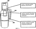
В соответствии с вариантом осуществления настоящего изобретения, CogniSensors представляют собой идеальное средство для выполнения автоматизированного контроля на производстве. Как показано на фиг.8, для проверки бутылки с водой может быть использован один или более CogniSensors. В этом примере, для контроля трех различных областей, названных Эксперт 1-3, используется три разных CogniSensors. Общая оценка определяется объединением оценок трех проверяющих CogniSensors. В данном примере CogniSensor 1 (Эксперт 1) может быть настроен на классификацию сигнатур ROI, содержащих крышку 802 бутылки. CogniSensor 1 может классифицировать свою ROI по двум категориям: Плохо и Хорошо. В категорию Плохо объединены следующие случаи: крышка отсутствует или крышка неправильно закручена.In accordance with an embodiment of the present invention, CogniSensors are an ideal means for performing automated production control. As shown in FIG. 8, one or more CogniSensors can be used to test a water bottle. In this example, three different CogniSensors are used to control three different areas, called Expert 1-3. The overall rating is determined by the combination of the ratings of the three CogniSensors reviewers. In this example, CogniSensor 1 (Expert 1) can be configured to classify ROI signatures containing 802 bottle caps.
Аналогично, CogniSensor 2 (Эксперт 2) может выучить сигнатуры ROI пересечения уровня 804 жидкости в бутылке. ROI может представлять собой узкий вертикально расположенный прямоугольник, который, в идеальном случае, перекрывает минимальный и максимальный возможные уровни заполнения бутылки. В зависимости от принятых производителем критериев контроля качества, CogniSensor 2 может классифицировать свою область интереса (ROI) по любому числу категорий, например Приемлемо и Неприемлемо; Слишком Высоко, Приемлемо и Слишком Низко; или Слишком Высоко, Высоко, но Приемлемо, В поле допуска, Низко, но Приемлемо, Слишком Низко.Similarly, CogniSensor 2 (Expert 2) can learn the ROI signatures of the intersection of the 804 liquid level in the bottle. An ROI can be a narrow, vertically positioned rectangle that ideally covers the minimum and maximum possible fill levels of a bottle. Depending on the quality control criteria adopted by the manufacturer,
CogniSensor 3 (Эксперт 3) может выучить сигнатуры области интереса, покрывающей область 806 наклейки. CogniSensor 3 может быть настроен на распознавание различных признаков или комбинаций признаков, например: Отсутствие наклейки, Дефект наклейки (порвана, поцарапана или загнута), неправильное расположение наклейки (перевернута, наклонена) и Хорошо.CogniSensor 3 (Expert 3) can learn the signatures of the region of interest covering the
Выходной сигнал из CogniSensors 1-3 может быть подан на контроллер, включенный в систему автоматизации процесса изготовления, для совершения соответствующих действий на базе принятого решения.The output signal from CogniSensors 1-3 can be fed to the controller included in the automation system of the manufacturing process, to perform appropriate actions based on the decision.
В соответствии с вариантом осуществления настоящего изобретения, CogniSensors могут быть оформлены в виде отдельных узлов, образуя "интеллектуальные" фоточувствительные ячейки или микролинзы. Такие устройства могут применяться в самых различных областях, например для обнаружения движущихся деталей, определения траекторий или направления по заданному маршруту движущихся деталей в процессе механической сборки (фиг.9А); для биометрической идентификации, например, в телефоне с фотокамерой (фиг.9Б); либо для обнаружения посетителей и идентификации в дверной глазок и т.п. (фиг.9В).According to an embodiment of the present invention, CogniSensors can be designed as separate units to form “smart” photosensitive cells or microlenses. Such devices can be used in various fields, for example, for detecting moving parts, determining trajectories or directions along a given route of moving parts during mechanical assembly (Fig. 9A); for biometric identification, for example, in a telephone with a camera (FIG. 9B); or to detect visitors and identify in the peephole, etc. (Fig. 9B).
В соответствии с другим вариантом осуществления настоящего изобретения, предложена система обнаружения для предупреждения водителя. Как показано на фиг.10, один или более CogniSensor 104 может быть встроен в ветровое стекло, индикаторную панель приборного щитка или фары автомобиля. CogniSensors 104 могут быть обучены распознавать образы, указывающие на потерю внимания водителем (например, водитель засыпает), и выдавать сигнал, включающий сигнализацию. Эти образы могут включать отслеживание взгляда, распознавание лица, распознавание выражения лица и др. Кроме того, CogniSensors 104, находящиеся в ветровом стекле или фаре, могут быть обучены распознавать объекты или события снаружи транспортного средства, например обнаруживать дождевые капли для работы дворников лобового стекла, или источники опасности на дороге для системы предупреждения об опасности на дороге.In accordance with another embodiment of the present invention, a detection system for warning a driver is provided. As shown in FIG. 10, one or
Обнаружение случайно появляющегося объекта в дальнем или ближнем поле зрения может быть выполнено рядом способов. Например, два или три чувствительных элемента могут быть оснащены линзами, сфокусированными на разные дальности. В чувствительные элементы может быть загружено одинаковое знание, но работать они будут с областями интереса разного размера. Общая реакция системы распознавания может считаться положительной, если хотя бы один чувствительный элемент распознает объект.The detection of a randomly appearing object in the far or near field of view can be performed in a number of ways. For example, two or three sensing elements can be equipped with lenses focused on different ranges. The same knowledge can be loaded into sensitive elements, but they will work with areas of interest of different sizes. The overall reaction of the recognition system can be considered positive if at least one sensitive element recognizes the object.
Далее, в конструкции CogniSensors могут использоваться входные чувствительные элементы, чувствительные на разных длинах волн, например ближнем инфракрасном и инфракрасном диапазонах, в узкой полосе, ограниченной фильтром и т.д. Для данного объекта или сцены, эти CogniSensors выдадут различные значения для пикселов, но могут быть обучены распознавать категории объектов по своим соответствующим видеоизображениям. При сопровождении целей, комбинация CogniSensors ближнего инфракрасного и инфракрасного диапазонов обеспечит распознавание цели в любое время суток.Further, CogniSensors can use input sensors that are sensitive at different wavelengths, such as near infrared and infrared, in a narrow band bounded by a filter, etc. For a given object or scene, these CogniSensors will give out different values for the pixels, but can be trained to recognize categories of objects from their respective video images. Accompanied by targets, a combination of CogniSensors near infrared and infrared ranges will provide target recognition at any time of the day.
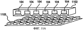
В соответствии с другим вариантом осуществления настоящего изобретения, решетки CogniSensors могут использоваться во многих иных производственных процессах. Например, как показано на фиг.11А, одномерная решетка CogniSensors 1102 может быть использована для контроля качества стеклянных поплавков 1103 при их изготовлении. На фиг.11Б показана двумерная решетка CogniSensors 1104, используемая для обнаружения загрязнений на дне контейнеров 1105, например бутылок для напитков. В таких применениях, CogniSensors могут быть обучены определению образов, показывающих дефекты в стекле или загрязнения в жидкости.In accordance with another embodiment of the present invention, CogniSensors grids can be used in many other manufacturing processes. For example, as shown in FIG. 11A, the one-
Согласно другому варианту осуществления настоящего изобретения. CogniSensors могут быть распределены, например, по стеклянной панели для выполнения многих независимых функций. CogniSensors могут быть сгруппированы, и каждые группы могут быть обучены своему знанию. На фиг.12 показана, в качестве примера, раздвижная дверь 1202, в которой имеется несколько групп CogniSensors 1204 для обнаружения приближающихся объектов различного размера. Первая группа может быть обучена знанию для распознавания первого размера 1208 человека или животного (например, собаки), вторая группа может быть обучена для распознавания человека другого размера (например, мальчика) 1210, третья группа - для человека третьего размера (например, взрослого) 1212, и так далее. Каждая группа 1204 может быть соединена с одной или более CogniMems 1206 для управления раздвижными дверями.According to another embodiment of the present invention. CogniSensors can be distributed, for example, over a glass panel to perform many independent functions. CogniSensors can be grouped, and each group can be trained in their knowledge. 12 shows, by way of example, a sliding door 1202 in which there are several groups of
Для специалиста, ознакомившегося с настоящим описанием, должно быть очевидно, что предложенный в изобретении формирователь изображения может быть использован для многочисленных, не упомянутых здесь, применений. Например, это может быть обнаружение остаточных повреждений (изменение текстуры) в плотине, мосту или ином сооружении. Реализация этого применения должна быть очевидной с учетом приведенного описания вариантов осуществления настоящего изобретения. Кроме того, передача энергии и сигналов может быть беспроводной (например, по инфракрасному каналу, посредством фотоэлемента, петли индуктивности и др.).For a person skilled in the art, it should be obvious that the imaging device proposed in the invention can be used for numerous applications not mentioned here. For example, it can be the detection of residual damage (texture change) in a dam, bridge or other structure. The implementation of this application should be apparent in view of the above description of embodiments of the present invention. In addition, the transmission of energy and signals can be wireless (for example, through the infrared channel, through a photocell, inductance loop, etc.).
Таким образом, выше были подробно описаны, со ссылками на чертежи, несколько предпочтительных вариантов осуществления изобретения. Хотя описание изобретения было основано на этих предпочтительных вариантах осуществления, для специалиста должно быть очевидным, что для описанных вариантов возможны определенные модификации, изменения и конструктивные исполнения, не выходящие за пределы существа и области патентных притязаний изобретения.Thus, several preferred embodiments of the invention have been described in detail above with reference to the drawings. Although the description of the invention was based on these preferred embodiments, it should be apparent to one skilled in the art that certain modifications, changes and designs are possible for the described options without departing from the spirit and scope of the patent claims of the invention.
Claims (34)
один или более фоточувствительных элементов, встроенных в прозрачную или полупрозрачную подложку или расположенных на ней, и
обрабатывающий элемент, соединенный с одним или более фоточувствительными элементами, встроенный в подложку или расположенный на ней и включающий одну или более нейронных цепей, причем прозрачная или полупрозрачная подложка образует оптический интерфейс между воспринимаемым падающим изображением и одним или более фоточувствительными элементами, и
конфигурация каждого фоточувствительного элемента обеспечивает выдачу им сигнала, зависящего от поступающего на его вход света, а конфигурация обрабатывающего элемента обеспечивает распознавание им образа, формируемого выходными сигналами фоточувствительных элементов.1. The pattern recognition device, including
one or more photosensitive elements embedded in or located on a transparent or translucent substrate, and
a processing element coupled to one or more photosensitive elements embedded in or located on a substrate and including one or more neural circuits, the transparent or translucent substrate forming an optical interface between the perceived incident image and one or more photosensitive elements, and
the configuration of each photosensitive element provides them with a signal that depends on the light arriving at its input, and the configuration of the processing element ensures recognition of the image formed by the output signals of the photosensitive elements.
множество воспринимающих элементов, расположенных на прозрачной или полупрозрачной подложке, каждый из которых включает:
фоточувствительный элемент, и
обучаемую нейронную цепь, связанную с фоточувствительным элементом,
множество оптических интерфейсов, сформированных на подложке, каждый из которых оптически связан с соответствующим одним из упомянутых воспринимающих элементов,
причем конфигурация фоточувствительного элемента обеспечивает выдачу им сигнала, зависящего от поступающего на его вход света, а конфигурация нейронной цепи обеспечивает распознавание ею образа, формируемого выходными сигналами фоточувствительных элементов.9. A pattern recognition device including
many sensing elements located on a transparent or translucent substrate, each of which includes:
photosensitive element, and
a trained neural circuit associated with a photosensitive element,
a plurality of optical interfaces formed on a substrate, each of which is optically coupled to a corresponding one of said sensing elements,
moreover, the configuration of the photosensitive element provides them with a signal that depends on the light arriving at its input, and the configuration of the neural circuit ensures that it recognizes the image formed by the output signals of the photosensitive elements.
прозрачную или полупрозрачную подложку,
множество фотодетекторов, каждый из которых встроен в подложку и имеет конфигурацию, обеспечивающую выдачу сигнала, основанного на поступившем на вход свете,
множество обучаемых нейронных цепей, каждая из которых встроена в подложку и имеет конфигурацию, обеспечивающую распознавание образа, основанного на выходных сигналах фотодетекторов, и выдачу сигнала, основанного на распознанном образе, и
средство оптического интерфейса для создания оптического интерфейса с множеством фотодетекторов.18. An image recognition device including
transparent or translucent substrate
many photodetectors, each of which is embedded in the substrate and has a configuration that provides a signal based on the light received at the input,
many trained neural circuits, each of which is embedded in the substrate and has a configuration that provides recognition of the image based on the output signals of photodetectors, and the issuance of a signal based on the recognized image, and
optical interface means for creating an optical interface with a plurality of photodetectors.
при этом конфигурация фоточувствительного элемента обеспечивает выдачу сигнала, поступившего на вход логической схемы представления данных, а конфигурация нейронов обеспечивает распознавание образа, основанного на сигналах, выданных логической схемой представления данных.29. An image recognition device comprising a combination of neurons with a photosensitive element and a logic diagram for presenting data embedded in a transparent or translucent substrate or located on it, and
the configuration of the photosensitive element provides the output of the signal received at the input of the logic of the data representation, and the configuration of the neurons provides recognition of the image based on the signals issued by the logic of the data representation.
встраивания в прозрачную или полупрозрачную подложку или нанесения на нее множества фотодетекторов и множества обучаемых нейронных цепей, и
использования средства оптического интерфейса для создания оптического интерфейса для множества фотодетекторов,
причем конфигурация каждого из множества фотодетекторов обеспечивает выдачу сигнала, основанного на поступившем на вход свете, а
конфигурация множества обучаемых нейронных цепей обеспечивает распознавание образа, основанного на выходных сигналах фотодетекторов, и выдачу сигнала, основанного на распознанном образе.30. A method of manufacturing an image recognition device, including steps
embedding in a transparent or translucent substrate or applying to it many photodetectors and many trained neural circuits, and
using optical interface means to create an optical interface for a variety of photodetectors,
moreover, the configuration of each of the many photodetectors provides a signal based on the incoming light, and
the configuration of the set of trained neural circuits provides recognition of an image based on the output signals of photodetectors, and the issuance of a signal based on a recognized image.
использование множества оптических интерфейсов, встроенных в прозрачную или полупрозрачную подложку или расположенных на ней, для создания оптического пути к одному или более фоточувствительным элементам, встроенным в подложку или расположенным на ней,
выдачу сигнала каждого из одного или более фоточувствительных элементов, основанного на поступившем на вход свете,
распознавание образа по выходным сигналам одного или более фоточувствительных элементов посредством параллельной обработки выходных сигналов одного или более фоточувствительных элементов в одном или более обрабатывающих элементах, каждый из которых соединен с одним из фоточувствительных элементов и встроен в подложку или расположен на ней,
причем упомянутые один или более обрабатывающих элементов включают одну или более нейронных цепей. 34. A method for pattern recognition, including:
the use of multiple optical interfaces embedded in or located on a transparent or translucent substrate to create an optical path to one or more photosensitive elements embedded in or located on the substrate,
issuing a signal of each of one or more photosensitive elements based on the light received at the input,
pattern recognition by the output signals of one or more photosensitive elements by parallel processing of the output signals of one or more photosensitive elements in one or more processing elements, each of which is connected to one of the photosensitive elements and is embedded in or located on the substrate,
moreover, said one or more processing elements include one or more neural circuits.
Applications Claiming Priority (2)
| Application Number | Priority Date | Filing Date | Title |
|---|---|---|---|
| US69498805P | 2005-06-30 | 2005-06-30 | |
| US60/694,988 | 2005-06-30 |
Publications (2)
| Publication Number | Publication Date |
|---|---|
| RU2008102837A RU2008102837A (en) | 2009-08-10 |
| RU2444059C2 true RU2444059C2 (en) | 2012-02-27 |
Family
ID=37192296
Family Applications (1)
| Application Number | Title | Priority Date | Filing Date |
|---|---|---|---|
| RU2008102837/08A RU2444059C2 (en) | 2005-06-30 | 2006-06-30 | Integrated device and method of reading images |
Country Status (10)
| Country | Link |
|---|---|
| US (1) | US7796841B2 (en) |
| EP (1) | EP1899899A1 (en) |
| JP (1) | JP4734410B2 (en) |
| KR (1) | KR101326384B1 (en) |
| CN (1) | CN101253515B (en) |
| BR (1) | BRPI0613097B1 (en) |
| CA (1) | CA2613922C (en) |
| MX (1) | MX2007016556A (en) |
| RU (1) | RU2444059C2 (en) |
| WO (1) | WO2007005688A1 (en) |
Cited By (2)
| Publication number | Priority date | Publication date | Assignee | Title |
|---|---|---|---|---|
| RU2715876C1 (en) * | 2016-04-14 | 2020-03-03 | Ниссан Мотор Ко., Лтд. | Method and equipment for displaying neighbourhoods of mobile body |
| RU2766420C2 (en) * | 2016-05-13 | 2022-03-15 | Белрон Интернешнл Лтд | Device and method for damage analysis |
Families Citing this family (16)
| Publication number | Priority date | Publication date | Assignee | Title |
|---|---|---|---|---|
| US8478081B2 (en) * | 2005-06-30 | 2013-07-02 | Agc Flat Glass North America, Inc. | Monolithic image perception device and method |
| US8798148B2 (en) * | 2007-06-15 | 2014-08-05 | Physical Optics Corporation | Apparatus and method employing pre-ATR-based real-time compression and video frame segmentation |
| EP2148204B1 (en) * | 2008-07-25 | 2013-01-02 | F. Hoffmann-La Roche AG | A laboratory storage and retrieval system and a method to handle laboratory sample tubes |
| EP2148206B1 (en) | 2008-07-25 | 2015-11-18 | F.Hoffmann-La Roche Ag | A laboratory system for handling sample tube racks, an alignmemt element for sample tube racks and a rack tray receiver assembly |
| ES2582205T3 (en) | 2008-07-25 | 2016-09-09 | F. Hoffmann-La Roche Ag | Laboratory method and system for handling sample tube racks |
| ES2402225T3 (en) * | 2008-07-25 | 2013-04-29 | F. Hoffmann-La Roche Ag | A method and a laboratory system for handling sample tubes and an image analysis unit |
| US8755515B1 (en) | 2008-09-29 | 2014-06-17 | Wai Wu | Parallel signal processing system and method |
| CN101902619A (en) * | 2010-06-22 | 2010-12-01 | 浙江天鸿汽车用品有限公司 | Vehicle-mounted intelligent identity recognizing and monitoring system |
| JP7728756B2 (en) | 2019-10-29 | 2025-08-25 | エイエムエス-オスラム インターナショナル ゲーエムベーハー | Optoelectronic Devices |
| US12300674B2 (en) | 2019-12-06 | 2025-05-13 | Osram Opto Semiconductors Gmbh | Optoelectronic device |
| JP7646649B2 (en) | 2019-12-06 | 2025-03-17 | エイエムエス-オスラム インターナショナル ゲーエムベーハー | DEVICE COMPRISING A CARRIER HAVING OPTOELECTRONIC DEVICES AND METHOD FOR MANUFACTURING SAME |
| CN114786944A (en) | 2019-12-06 | 2022-07-22 | 奥斯兰姆奥普托半导体股份有限两合公司 | Window pane or surface of a vehicle comprising at least one optoelectronic component |
| US12040317B2 (en) | 2019-12-06 | 2024-07-16 | Osram Opto Semiconductors Gmbh | Optoelectronic device |
| US12328983B2 (en) | 2019-12-06 | 2025-06-10 | Osram Opto Semiconductors Gmbh | Optoelectronic arrangement |
| CN111104542B (en) * | 2020-01-07 | 2023-04-18 | 成都睿琪科技有限责任公司 | Part identification management method and device |
| WO2021188755A1 (en) * | 2020-03-18 | 2021-09-23 | Gentex Corporation | Near infra-red emitting rearview assembly |
Citations (4)
| Publication number | Priority date | Publication date | Assignee | Title |
|---|---|---|---|---|
| EP0526504B1 (en) * | 1990-04-26 | 1997-01-15 | SUTHERLAND, John | Artificial neural device |
| RU94043709A (en) * | 1991-12-30 | 1997-12-20 | Информейшн Оптикс Корпорейшн | OPTICAL MEMORY DEVICE WITH RANDOM ACCESS |
| EP0893915A2 (en) * | 1997-06-25 | 1999-01-27 | Eastman Kodak Company | Compact image sensor with display integrally attached |
| US6332137B1 (en) * | 1999-02-11 | 2001-12-18 | Toshikazu Hori | Parallel associative learning memory for a standalone hardwired recognition system |
Family Cites Families (16)
| Publication number | Priority date | Publication date | Assignee | Title |
|---|---|---|---|---|
| JPS63161680A (en) * | 1986-12-25 | 1988-07-05 | Mitsubishi Electric Corp | Semiconductor photodetector |
| DE69430744T2 (en) | 1994-07-28 | 2003-01-30 | International Business Machines Corp., Armonk | Improved neural semiconductor chip architectures and neural networks in them |
| EP0694856B1 (en) | 1994-07-28 | 2002-05-02 | International Business Machines Corporation | Daisy chain circuit for serial connection of neuron circuits |
| EP0694852B1 (en) | 1994-07-28 | 2002-06-26 | International Business Machines Corporation | Innovative neuron circuit architectures |
| EP0694855B1 (en) | 1994-07-28 | 2002-05-02 | International Business Machines Corporation | Search/sort circuit for neural networks |
| DE69430527T2 (en) | 1994-07-28 | 2003-01-02 | International Business Machines Corp., Armonk | Circuit for precharging input vector components into a free neuron circuit during the detection phase |
| TW409253B (en) * | 1997-09-29 | 2000-10-21 | Siemens Ag | Associative memory and its operation method |
| US7242449B1 (en) * | 1999-07-23 | 2007-07-10 | Semiconductor Energy Laboratory Co., Ltd. | Semiconductor device and integral image recognition/display apparatus |
| US6221687B1 (en) * | 1999-12-23 | 2001-04-24 | Tower Semiconductor Ltd. | Color image sensor with embedded microlens array |
| US6606614B1 (en) * | 2000-08-24 | 2003-08-12 | Silicon Recognition, Inc. | Neural network integrated circuit with fewer pins |
| JP4258393B2 (en) * | 2003-03-13 | 2009-04-30 | 三菱電機株式会社 | Personal identification device, fingerprint image pickup device, and fingerprint image acquisition method |
| KR100964586B1 (en) * | 2003-04-25 | 2010-06-21 | 삼성전자주식회사 | Fingerprint recognition device and liquid crystal display device having same |
| JP2005167090A (en) * | 2003-12-04 | 2005-06-23 | Hamamatsu Photonics Kk | Semiconductor light receiving element and manufacturing method therefor |
| US7019391B2 (en) * | 2004-04-06 | 2006-03-28 | Bao Tran | NANO IC packaging |
| US7643203B2 (en) * | 2006-04-10 | 2010-01-05 | Qualcomm Mems Technologies, Inc. | Interferometric optical display system with broadband characteristics |
| US7488950B2 (en) * | 2006-06-05 | 2009-02-10 | Blaise Laurent Mouttet | Crosswire sensor |
-
2006
- 2006-06-30 EP EP06786060A patent/EP1899899A1/en not_active Withdrawn
- 2006-06-30 CN CN2006800315217A patent/CN101253515B/en not_active Expired - Fee Related
- 2006-06-30 CA CA2613922A patent/CA2613922C/en not_active Expired - Fee Related
- 2006-06-30 MX MX2007016556A patent/MX2007016556A/en active IP Right Grant
- 2006-06-30 JP JP2008519641A patent/JP4734410B2/en not_active Expired - Fee Related
- 2006-06-30 RU RU2008102837/08A patent/RU2444059C2/en not_active IP Right Cessation
- 2006-06-30 US US11/477,571 patent/US7796841B2/en not_active Expired - Fee Related
- 2006-06-30 BR BRPI0613097A patent/BRPI0613097B1/en not_active IP Right Cessation
- 2006-06-30 WO PCT/US2006/025731 patent/WO2007005688A1/en not_active Ceased
- 2006-06-30 KR KR1020087002422A patent/KR101326384B1/en not_active Expired - Fee Related
Patent Citations (5)
| Publication number | Priority date | Publication date | Assignee | Title |
|---|---|---|---|---|
| EP0526504B1 (en) * | 1990-04-26 | 1997-01-15 | SUTHERLAND, John | Artificial neural device |
| RU2193797C2 (en) * | 1990-04-26 | 2002-11-27 | Джон СУТЕРЛАНД | Content-addressable memory device (alternatives) and image identification method (alternatives) |
| RU94043709A (en) * | 1991-12-30 | 1997-12-20 | Информейшн Оптикс Корпорейшн | OPTICAL MEMORY DEVICE WITH RANDOM ACCESS |
| EP0893915A2 (en) * | 1997-06-25 | 1999-01-27 | Eastman Kodak Company | Compact image sensor with display integrally attached |
| US6332137B1 (en) * | 1999-02-11 | 2001-12-18 | Toshikazu Hori | Parallel associative learning memory for a standalone hardwired recognition system |
Non-Patent Citations (1)
| Title |
|---|
| VITADLE S ET AL "MULTI - LAYER PERCEPTRON MAPPING ON A SIMD ARCHITECTURE" NEURAL NETWORKS FOR SIGNAL PROCESSING, 2002, PROCEEDING OF THE 2002 12 TH IEEE WORKSHOP ON SEP 4-6, 2002, PISCATAWAY, NJ, USA, IEEE, 04.09.2002, ISBN: 0-7803-7616-1. * |
Cited By (3)
| Publication number | Priority date | Publication date | Assignee | Title |
|---|---|---|---|---|
| RU2715876C1 (en) * | 2016-04-14 | 2020-03-03 | Ниссан Мотор Ко., Лтд. | Method and equipment for displaying neighbourhoods of mobile body |
| RU2766420C2 (en) * | 2016-05-13 | 2022-03-15 | Белрон Интернешнл Лтд | Device and method for damage analysis |
| US11692949B2 (en) | 2016-05-13 | 2023-07-04 | Belron International Limited | Break analysis apparatus and method |
Also Published As
| Publication number | Publication date |
|---|---|
| BRPI0613097B1 (en) | 2019-01-22 |
| KR101326384B1 (en) | 2013-11-11 |
| CA2613922A1 (en) | 2007-01-11 |
| JP2009524120A (en) | 2009-06-25 |
| US20070014469A1 (en) | 2007-01-18 |
| WO2007005688A1 (en) | 2007-01-11 |
| JP4734410B2 (en) | 2011-07-27 |
| KR20080038319A (en) | 2008-05-06 |
| CN101253515B (en) | 2012-09-26 |
| CA2613922C (en) | 2015-06-16 |
| US7796841B2 (en) | 2010-09-14 |
| EP1899899A1 (en) | 2008-03-19 |
| MX2007016556A (en) | 2008-03-07 |
| BRPI0613097A2 (en) | 2010-12-21 |
| RU2008102837A (en) | 2009-08-10 |
| WO2007005688A9 (en) | 2007-02-22 |
| CN101253515A (en) | 2008-08-27 |
Similar Documents
| Publication | Publication Date | Title |
|---|---|---|
| RU2444059C2 (en) | Integrated device and method of reading images | |
| RU2585985C2 (en) | Integral image pickup apparatus and method | |
| US10394406B2 (en) | Touch display device | |
| CN116912485A (en) | A scene semantic segmentation method based on the fusion of thermal image and visible light image features | |
| US8514280B2 (en) | Method and system for detecting an individual by means of passive infrared sensors | |
| JP2018136211A (en) | Environment recognition system and learning apparatus | |
| CN111126271A (en) | Bayonet snap-shot image vehicle detection method, computer storage medium and electronic device | |
| JP7769915B2 (en) | Information processing device, information processing system, information processing method, and information processing program | |
| JP7695642B2 (en) | Information processing device, information processing system, information processing method, and information processing program | |
| TWI463418B (en) | Monolithic image perception device and method | |
| JP4604816B2 (en) | In-vehicle imaging module | |
| US20250131533A1 (en) | Image processing device and operating method thereof | |
| CN121190901A (en) | Systems and training methods for training multi-task models |
Legal Events
| Date | Code | Title | Description |
|---|---|---|---|
| MM4A | The patent is invalid due to non-payment of fees |
Effective date: 20200701 |