RU2345388C1 - Optical device of laser resonator (versions) - Google Patents
Optical device of laser resonator (versions) Download PDFInfo
- Publication number
- RU2345388C1 RU2345388C1 RU2007112036/28A RU2007112036A RU2345388C1 RU 2345388 C1 RU2345388 C1 RU 2345388C1 RU 2007112036/28 A RU2007112036/28 A RU 2007112036/28A RU 2007112036 A RU2007112036 A RU 2007112036A RU 2345388 C1 RU2345388 C1 RU 2345388C1
- Authority
- RU
- Russia
- Prior art keywords
- surface layer
- reflection
- optical element
- recesses
- protrusions
- Prior art date
Links
- 230000003287 optical effect Effects 0.000 title claims abstract description 68
- 230000005540 biological transmission Effects 0.000 claims abstract description 28
- 239000000463 material Substances 0.000 claims abstract description 17
- 230000014509 gene expression Effects 0.000 claims abstract description 11
- 239000002344 surface layer Substances 0.000 claims description 36
- 238000002834 transmittance Methods 0.000 claims description 26
- 239000010410 layer Substances 0.000 claims description 15
- 239000000126 substance Substances 0.000 abstract description 6
- 238000002310 reflectometry Methods 0.000 abstract 3
- 230000000694 effects Effects 0.000 abstract 1
- 230000005855 radiation Effects 0.000 description 16
- 239000000758 substrate Substances 0.000 description 8
- 230000004907 flux Effects 0.000 description 6
- 238000004519 manufacturing process Methods 0.000 description 6
- 238000000576 coating method Methods 0.000 description 3
- 230000003595 spectral effect Effects 0.000 description 3
- 229910004298 SiO 2 Inorganic materials 0.000 description 2
- 238000005530 etching Methods 0.000 description 2
- 239000002184 metal Substances 0.000 description 2
- 238000000034 method Methods 0.000 description 2
- 230000010363 phase shift Effects 0.000 description 2
- 239000011248 coating agent Substances 0.000 description 1
- 230000007423 decrease Effects 0.000 description 1
- 230000003111 delayed effect Effects 0.000 description 1
- 238000010586 diagram Methods 0.000 description 1
- 238000000206 photolithography Methods 0.000 description 1
- 238000001020 plasma etching Methods 0.000 description 1
- 239000010453 quartz Substances 0.000 description 1
- VYPSYNLAJGMNEJ-UHFFFAOYSA-N silicon dioxide Inorganic materials O=[Si]=O VYPSYNLAJGMNEJ-UHFFFAOYSA-N 0.000 description 1
- 238000004611 spectroscopical analysis Methods 0.000 description 1
- 238000001228 spectrum Methods 0.000 description 1
- 238000012876 topography Methods 0.000 description 1
Images


Landscapes
- Lasers (AREA)
Abstract
Description
Изобретение относится к лазерной оптике и может быть использовано как оптический элемент лазерного резонатора (градиентное зеркало или «мягкая» диафрагма) при работе с твердотельными и газовыми лазерами для формирования заданного закона распределения оптического излучения, а также в астрономии и спектроскопии для коррекции формы оптической передаточной функции.The invention relates to laser optics and can be used as an optical element of a laser resonator (gradient mirror or “soft” aperture) when working with solid-state and gas lasers to form a given law for the distribution of optical radiation, as well as in astronomy and spectroscopy to correct the shape of the optical transfer function .
Известен оптический элемент лазерного резонатора, выполненный в виде зеркала с гауссовым распределением коэффициента отражения (Н.Р.Белашенков, В.Б.Карасев, Э.С.Путилин, П.Н.Фимин, В.Ю.Храмов. Градиентные лазерные зеркала. Оптический журнал, 2001, т.68, №5, стр.9-19). Многослойное диэлектрическое покрытие выполнено с переменным по поверхности зеркала распределением толщины. В дальней зоне распределение интенсивности излучения лазера с таким зеркалом не имеет дополнительных максимумов.Known optical element of the laser resonator, made in the form of a mirror with a Gaussian distribution of the reflection coefficient (N.R. Belashenkov, V. B. Karasev, E. S. Putilin, P. N. Fimin, V. Yu. Khramov. Gradient laser mirrors. Optical Journal, 2001, vol. 68, No. 5, pp. 9-19). The multilayer dielectric coating is made with a variable thickness distribution over the surface of the mirror. In the far zone, the distribution of the laser radiation intensity with such a mirror has no additional maxima.
Однако изготовление таких зеркал сопряжено с большой сложностью создания многослойных зеркал с переменной по поверхности толщиной и необходимостью изготовления для этого специальных диафрагм. Кроме того, существенным недостатком данного оптического элемента лазерного резонатора является невозможность обеспечения произвольно заданного закона распределения пропускания. Кроме того, из-за того, что диэлектрические структуры выполняются с переменной по поверхности толщиной, возникают паразитные фазовые сдвиги, которые нарушают работу резонатора лазера.However, the manufacture of such mirrors is associated with the great difficulty of creating multilayer mirrors with a variable surface thickness and the need to produce special diaphragms for this. In addition, a significant drawback of this optical element of the laser cavity is the impossibility of providing an arbitrarily specified transmission law. In addition, due to the fact that the dielectric structures are performed with a thickness that is variable over the surface, spurious phase shifts occur that disrupt the operation of the laser cavity.
Известен также оптический элемент лазерного резонатора, выполненный в виде кюветы с двумя окнами, установленными с зазором, нарастающим от оси кюветы к периферии и заполненной рабочим веществом, ослабляющим оптическое излучение и содержащим оптические неоднородности с показателем преломления, отличными от показателя преломления основного рабочего вещества (Патент РФ №2163386, G02B 27/58. Мягкая диафрагма для лазеров. Сенатский Ю.В. Приоритет 19.03.1999 г. Опубликован 20.02.2001 г.).Also known is the optical element of the laser cavity, made in the form of a cuvette with two windows installed with a gap growing from the axis of the cuvette to the periphery and filled with a working substance, attenuating optical radiation and containing optical inhomogeneities with a refractive index different from the refractive index of the main working substance (Patent RF №2163386, G02B 27/58 Soft diaphragm for lasers. Senate Yu.V. Priority March 19, 1999 Published on February 20, 2001).
Недостатками данного изобретения являются сложность конструкции и невозможность получения произвольного профиля распределения интенсивности из-за технологических трудностей изготовления зазора произвольной толщины, сложность изготовления кюветы и рабочего вещества, низкая лучевая стойкость изготовления кюветы и рабочего вещества, низкая лучевая стойкость оптического элемента и большие световые потери.The disadvantages of this invention are the design complexity and the impossibility of obtaining an arbitrary intensity distribution profile due to technological difficulties in manufacturing a gap of arbitrary thickness, the complexity of manufacturing a cuvette and a working substance, low radiation resistance of a cell and a working substance, low radiation resistance of an optical element and high light losses.
Известен также оптический элемент лазерного резонатора, выполненный в виде подложки с нанесенной на нее рельефной металлической дифракционной решеткой (ДР) (Патент РФ №2166819, G02B 5/18, Оптический элемент лазерного резонатора. Низьев В.Г. Приоритет 15.06.1999 г. Опубликован 10.05 2001 г.).Also known is an optical element of a laser resonator made in the form of a substrate with a relief metal diffraction grating (DR) deposited on it (RF Patent No. 2166819,
Недостатками данного изобретения являются низкое значение коэффициента пропускания (или отражения), низкая лучевая стойкость, обусловленная применением поглощающей металлической ДР, и большие световые потери.The disadvantages of this invention are the low transmittance (or reflection), low radiation resistance due to the use of absorbing metal DR, and large light losses.
Наиболее близким по конструкции к предлагаемому изобретению является устройство, состоящее из пластины оптического материала с поверхностным слоем, выполненным в виде ДР со штрихами в виде последовательности углублений поверхностного слоя (Патент РФ №2137163, G02B 5/20. Светофильтр оптического излучения переменной плотности. А.Г.Полещук. Приоритет 10.12.1996 г., опубликован 10.09.1999 г.). Штрихи ДР выполнены в виде концентрических колец с переменной вдоль окружности шириной. Указанное устройство предназначено для создания фильтра с переменным пропусканием, и использовать его в качестве предлагаемого в заявке оптического элемента лазерного резонатора нельзя по следующим причинам:The closest in design to the proposed invention is a device consisting of a plate of optical material with a surface layer made in the form of DR with strokes in the form of a sequence of recesses of the surface layer (RF Patent No. 2137163,
1. Оно имеет низкое значение коэффициента пропускания (или отражения), обусловленного наличием непрерывных концентрических колец с переменной шириной. Коэффициент пропускания известного элемента определяется выражением:1. It has a low transmittance (or reflection) due to the presence of continuous concentric rings with a variable width. The transmittance of a known element is determined by the expression:
![]()
![]()
где d - ширина штриха, Т - период дифракционной решетки.where d is the stroke width, T is the period of the diffraction grating.
Из выражения (1) следует, что при значениях Т=5-10 мкм и dmin=1-2 мкм максимальное светопропускание известного устройства составляет ![]()
![]()
2. При использовании указанного устройства возможен только угловой закон изменения пропускания, что не позволяет формирование известным изобретением наиболее часто встречающейся на практике супергауссовой радиальной зависимости коэффициента пропускания (отражения) элемента:2. When using the specified device, only the angular law of the transmission variation is possible, which does not allow the well-known invention to form the super Gaussian radial dependence of the transmittance (reflection) of the element most often encountered in practice:
![]()
![]()
где r - расстояние до центра, G0 - коэффициент пропускания (отражения) в центре, w - расстояние до центра, при котором коэффициент отражения падает в е раз, N - порядок супергауссова закона.where r is the distance to the center, G 0 is the transmittance (reflection) in the center, w is the distance to the center at which the reflection coefficient drops e times, N is the order of the super-Gaussian law.
Однако по конструкции это устройство является наиболее близким к предлагаемому изобретению.However, in design this device is the closest to the proposed invention.
Технической задачей предлагаемого изобретения является создание оптического элемента лазерного резонатора, имеющего высокое значение коэффициента пропускания (отражения), обладающего функцией отражения или пропускания с произвольно заданным законом изменения и обеспечивающего аподизацию лазерных пучков в широком спектральном диапазоне (например, с двумерной супергауссовой зависимостью коэффициента пропускания/отражения) и в то же время имеющего высокую лучевую стойкость.The technical task of the invention is the creation of an optical element of a laser resonator having a high transmittance (reflection), having a reflection or transmitting function with an arbitrarily specified law of change, and providing apodization of laser beams in a wide spectral range (for example, with a two-dimensional super-Gaussian dependence of the transmittance / reflection ) and at the same time having high radiation resistance.
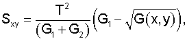
Поставленная задача выполнения произвольно заданного закона радиальной зависимости коэффициента пропускания (отражения) достигается в первом варианте за счет того, что в оптическом элементе лазерного резонатора, состоящем из пластины оптического материала (например, кварца) с поверхностным слоем, выполненным в виде дифракционной решетки со штрихами в виде последовательности углублений или выступов поверхностного слоя, площадь Sxy углубления в области поверхностного слоя с координатами x и y определяется по предложенной авторами формулеThe task of fulfilling an arbitrary given law of the radial dependence of the transmittance (reflection) is achieved in the first embodiment due to the fact that in the optical element of the laser resonator, consisting of a plate of optical material (for example, quartz) with a surface layer made in the form of a diffraction grating with strokes in in the form of a sequence of recesses or protrusions of the surface layer, the area S xy of the recess in the region of the surface layer with x and y coordinates is determined by the form proposed by the authors le

где Т - период следования углублений или выступов, G1 - коэффициент отражения или пропускания поверхностного слоя, ![]()
![]()
![]()
![]()
![]()
![]()
С целью увеличения коэффициента отражения (пропускания) на поверхность пластины нанесена многослойная диэлектрическая структура. Подобная высокоотражающая структура применяется в лазерных зеркалах, а также в просветляющих покрытиях.In order to increase the reflection coefficient (transmittance), a multilayer dielectric structure is applied to the surface of the plate. Such a highly reflective structure is used in laser mirrors, as well as in antireflection coatings.
При этом во втором варианте оптического элемента лазерного резонатора многослойная диэлектрическая структура дополнительно нанесена на дифракционную решетку, выполненную в поверхностном слое пластины в виде последовательности отличающихся по площади углублений или выступов, а в третьем варианте оптического элемента лазерного резонатора поверхностный слой образуется путем нанесения на пластину многослойной диэлектрической структуры, а дифракционная решетка, состоящая из последовательности отличающихся по площади углублений или выступов, выполнена во внешнем слое многослойной диэлектрической структуры. Период следования Т углублений или выступов штрихов решетки выбирается для всех вариантов по формулеIn this case, in the second embodiment of the optical element of the laser resonator, the multilayer dielectric structure is additionally deposited on the diffraction grating made in the surface layer of the plate in the form of a sequence of recesses or protrusions differing in area, and in the third embodiment of the optical element of the laser resonator, the surface layer is formed by applying a multilayer dielectric to the plate structures, and a diffraction grating consisting of a sequence of recesses differing in area or protrusions made in the outer layer of a multilayer dielectric structure. The repetition period T of the recesses or protrusions of the grating strokes is selected for all variants according to the formula
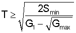
где ![]()
![]()
Технический результат заключается в том, что заявляемый оптический элемент лазерного резонатора имеет высокое значение коэффициента пропускания/отражения и функцию отражения/пропускания с произвольно заданным законом изменения, обеспечивает аподизацию лазерных пучков в широком спектральном диапазоне и в то же время имеет высокую лучевую стойкость из-за отсутствия поглощающих веществ в многослойных диэлектрических покрытиях. Достигнутое в устройстве увеличение коэффициента пропускания одновременно повышает контраст.The technical result consists in the fact that the inventive optical element of the laser resonator has a high transmittance / reflection coefficient and a reflection / transmittance function with an arbitrarily specified law of change, provides apodization of laser beams in a wide spectral range and at the same time has high radiation resistance due to lack of absorbing substances in multilayer dielectric coatings. The increase in transmittance achieved in the device simultaneously increases contrast.
Сущность изобретения поясняется графическими материалами.The invention is illustrated graphic materials.
На фиг.1 представлена схема оптического элемента лазерного резонатора в двух проекциях (а и б).Figure 1 presents a diagram of an optical element of a laser resonator in two projections (a and b).
На фиг.2. представлены примеры сечения оптического элемента с поверхностным слоем, выполненным в виде многослойной дифракционной структуры (а и б).In figure 2. examples of the cross section of an optical element with a surface layer made in the form of a multilayer diffraction structure (a and b) are presented.
На фиг.3 представлен пример осуществления заявляемого изобретения в качестве градиентного зеркала лазера.Figure 3 presents an example implementation of the claimed invention as a gradient mirror of the laser.
На фиг.4. представлены зависимости коэффициента пропускания (отражения) от площади углубления.In figure 4. The dependences of the transmittance (reflection) on the area of the depression are presented.
На фиг.5. представлены для сравнения два графика зависимости коэффициента отражения десятислойного диэлектрического зеркала от материала последнего слоя. На графике 1 последний слой изготовлен из ZnO2, на графике 2 - из SiO2.In Fig.5. two graphs of the dependence of the reflection coefficient of a ten-layer dielectric mirror on the material of the last layer are presented for comparison. In
Оптический элемент лазерного резонатора (фиг.1а) состоит из пластины оптического материала (подложки) 1 с поверхностным слоем 2, выполненным в виде дифракционной решетки со штрихами 3 в виде последовательности углублений поверхностного слоя. Дифракционная решетка имеет период Т и глубину профиля h (фиг.1б).The optical element of the laser resonator (figa) consists of a plate of optical material (substrate) 1 with a surface layer 2 made in the form of a diffraction grating with
На фиг.2 изображена подложка 1, на которую дополнительно нанесена многослойная диэлектрическая структура 4. Фиг.2а иллюстрирует выполнение пластины оптического элемента лазерного резонатора по первому варианту изобретения, а фиг.2б - по второму.Figure 2 shows the
Поясним подробнее конструкцию предлагаемого устройства. Поверхностный слой 2 (фиг.1) выполнен в виде дифракционной решетки со штрихами в виде последовательности углублений (или выступов) 3. Площадь S каждого углубления изменяется в зависимости от места на пластине. Углубления в поверхностном слое пластины имеют глубину h не более h=![]()
![]()
Поверхностным слоем подложки может служить дополнительно нанесенная многослойная диэлектрическая структура (МДС) 4, показанная на фиг.2. МДС наносят с целью повышения коэффициента пропускания или отражения. МДС 4 (Фиг.2а) может быть нанесена на поверхность дифракционной решетки, выполненной в материале подложки (изготовление оптического элемента по первому варианту предлагаемого изобретения). А по второму варианту предлагаемого устройства ДР выполняется не в материале подложки, а во внешнем слое МДС (фиг.2б). В первом случае вначале изготавливается ДР, а затем на нее производится напыление N слоев МДС. Во втором случае на поверхность пластины оптического материала 1 напыляются N слоев МДС. Во внешнем слое методом фотолитографии и реактивно-ионного травления формируется рельеф ДР. Так как слои МДС обычно выполняются из различных материалов, травление рисунка ДР по глубине осуществляется до полного стравливания внешнего слоя, предпочтительно выполненного из SiO2. При этом нижний слой играет роль стоп-слоя, что позволяет выполнить травление по глубине с высокой точностью.The surface layer of the substrate can serve as an additionally applied multilayer dielectric structure (MDS) 4, shown in figure 2. MDS is applied to increase transmittance or reflection. MDS 4 (Fig. 2a) can be deposited on the surface of a diffraction grating made in a substrate material (manufacturing an optical element according to the first embodiment of the present invention). And according to the second variant of the proposed device, DR is performed not in the substrate material, but in the outer layer of the MDS (fig.2b). In the first case, a DR is first manufactured, and then N layers of MDS are sprayed onto it. In the second case, N layers of MDS are sprayed onto the surface of the plate of the
На фиг.3 представлен пример использования заявляемого изобретения в качестве градиентного зеркала. Оптический элемент 1 лазерного резонатора устанавливается последовательно с активной средой 5 и зеркалом 6. Оптические оси отраженного светового потока Iref и прошедшего светового потока Iout ![]()
![]()
Световой поток, отражаясь от ДР, разлагается в угловой спектр на ряд дифракционных порядков. Нулевой порядок дифракции с интенсивностью I0 не изменяет направления распространения, а боковые дифракционные порядки распространяются под углами αk к оптической оси (фиг.3) и задерживаются входной апертурой активной среды 5. Интенсивность излучения в нулевом порядке дифракции, который является рабочим, на выходе элемента в скалярном приближении описывается выражениемThe light flux, reflected from the DR, is decomposed into the angular spectrum into a number of diffraction orders. The zero diffraction order with intensity I 0 does not change the direction of propagation, and the lateral diffraction orders propagate at angles α k to the optical axis (Fig. 3) and are delayed by the input aperture of the
![]()
![]()
где φ=2π·h(n-1) - фазовый сдвиг, вносимый штрихами ДР (В.Н.Котлецов. Микроизображения. Оптические методы получения и контроля. Л., Машиностроение, 1985, стр.210).where φ = 2π · h (n-1) is the phase shift introduced by the strokes of the DR (V.N. Kotletsov. Microimages. Optical methods of obtaining and control. L., Mashinostroenie, 1985, p. 210).
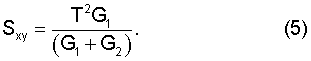
Для ДР с φ=π из выражения (3) следует, что коэффициент пропускания или отражения оптического элемента описывается выражениемFor a DR with φ = π, it follows from expression (3) that the transmittance or reflection of an optical element is described by the expression
![]()
![]()
где G1 - коэффициент отражения или пропускания поверхностного слоя подложки, G2 - коэффициент отражения или пропускания поверхностного слоя подложки в области углубления.where G 1 is the reflection or transmission coefficient of the surface layer of the substrate, G 2 is the reflection or transmission coefficient of the surface layer of the substrate in the region of the recess.
Если необходимо иметь заданную функцию G(x,y) изменения коэффициента отражения элемента или пропускания в зависимости от координат x и y, то, как следует из формулы (4), площадь углублений S решетки должна меняться по следующему закону:If it is necessary to have a given function G (x, y) of changing the reflection coefficient of the element or transmittance depending on the coordinates x and y, then, as follows from formula (4), the area of the recesses S of the lattice should change according to the following law:

где G(x,y) - заданная функция коэффициента отражения или пропускания оптического элемента лазерного резонатора вдоль координат x и y.where G (x, y) is the given function of the reflection or transmission coefficient of the optical element of the laser resonator along the x and y coordinates.
На фиг.4 представлены зависимости коэффициента пропускания (отражения) от площади углубления при Т=10 мкм, ![]()
![]()
![]()
![]()
Коэффициент отражения (пропускания) МДС незначительно меняется в области, где внешний слой удален для формирования углубления. На фиг.5 это изменение равно разности между пиковыми значениями графиков 1 и 2, которое уменьшается с увеличением количества слоев в МДС.The reflection coefficient (transmittance) of the MDS varies slightly in the region where the outer layer is removed to form a recess. In figure 5, this change is equal to the difference between the peak values of
Площадь углублений меняется от минимального значения Smin, определяемого технологией изготовления рельефа поверхности и длиной волны света dmin>λ, до некоторого максимального значения Smax, при котором коэффициент отражения (пропускания) элемента стремится к нулю G=0. Из выражения (4) следует, что при G=0 эта площадь определяется соотношениемThe area of the recesses varies from the minimum value S min determined by the technology of manufacturing the surface topography and the wavelength of light d min > λ to a certain maximum value S max at which the reflection (transmittance) of the element tends to zero G = 0. From expression (4) it follows that for G = 0 this area is determined by the relation
Т.е. при G1=G2~1 площадь Sxy=Т2/2. Существенным преимуществом предлагаемого технического решения является выбор произвольной формы углубления. В соответствии с выражениями (4) и (5) для обеспечения функции заданного пропускания или отражения необходимо обеспечить заданную величину площади, причем форма углубления существенного значения не имеет (возможное ограничение - резкие изгибы с радиусами менее длины волны света). Это позволяет существенно упростить изготовление ДР оптического элемента путем применения метода прямой записи импульсным лазером. В этом случае достаточно хорошо контролируется площадь снятого материала, в то время как форма обрабатываемой области меняется.Those. when G 1 = G 2 -1 area S xy = T 2/2. A significant advantage of the proposed technical solution is the choice of an arbitrary shape of the recess. In accordance with expressions (4) and (5), to ensure the function of a given transmittance or reflection, it is necessary to provide a given area value, and the shape of the recess is not significant (a possible limitation is sharp bends with radii less than the wavelength of light). This makes it possible to significantly simplify the fabrication of the DR of an optical element by applying the direct recording method by a pulsed laser. In this case, the area of the removed material is rather well controlled, while the shape of the treated area changes.
Величина Smin площади углублений определяется из соотношения их площади и глубины рельефа ДР по формулеThe value of S min the area of the recesses is determined from the ratio of their area and the depth of the relief DR according to the formula
![]()
![]()
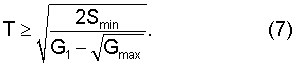
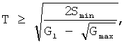
Период следования Т углублений определяется из выражения (4) при максимальном значении коэффициента отражения/пропускания G(x,y)=Gmax и минимально технологически выполнимой площади Smin углубленийThe repetition period T of the recesses is determined from expression (4) with a maximum reflection / transmission coefficient G (x, y) = G max and a minimally technologically feasible area S min of recesses
Предложенный оптический элемент имеет высокое светопропускание, или малые остаточное потери оптического излучения. Это делает возможным его использование в качестве внутрирезонаторного зеркала мощных лазеров. Конструкция оптического элемента лазерного резонатора обеспечивает функцию отражения или пропускания с высоким контрастом и произвольно заданным законом изменения для аподизации лазерных пучков в широком спектральном диапазоне и в то же время имеет высокую лучевую стойкость. Таким образом, предлагаемый оптический элемент обеспечивает новые возможности, отсутствующие у известных аналогов - малые потери света, простота конструкции и возможность эффективно формировать излучение мощных лазеров с заданным распределением оптического излучения.The proposed optical element has a high transmittance, or small residual loss of optical radiation. This makes it possible to use it as an intracavity mirror of high-power lasers. The design of the optical element of the laser resonator provides a reflection or transmission function with high contrast and an arbitrarily specified law of change for apodization of laser beams in a wide spectral range and at the same time has high radiation resistance. Thus, the proposed optical element provides new opportunities that are absent from the known analogues - low light loss, simplicity of design and the ability to effectively generate radiation from high-power lasers with a given distribution of optical radiation.
Claims (6)
где Т - период следования углублений или выступов, G1 - коэффициент отражения или пропускания поверхностного слоя, G2 - коэффициент отражения или пропускания поверхностного слоя в области углубления или выступа, G(x,y) - требуемая функция изменения коэффициента отражения или пропускания оптического элемента лазерного резонатора вдоль координат Х и Y.1. The optical element of the laser cavity, consisting of a plate of optical material with a surface layer made in the form of a diffraction grating with strokes in the form of a sequence of recesses or protrusions of the surface layer, characterized in that the area S xy of the recess or protrusion in the region of the surface layer with coordinates X and Y is determined from the expression
where T is the period of the recesses or protrusions, G 1 is the reflection or transmission coefficient of the surface layer, G 2 is the reflection or transmission coefficient of the surface layer in the region of the recess or protrusion, G (x, y) is the required function of changing the reflection coefficient or transmission of the optical element laser cavity along the X and Y coordinates.
где Т - период следования углублений или выступов, G1 - коэффициент отражения или пропускания поверхностного слоя, G2 - коэффициент отражения или пропускания поверхностного слоя в области углубления или выступов, G(x,y) - требуемая функция изменения коэффициента отражения или пропускания оптического элемента лазерного резонатора вдоль координат Х и Y.2. The optical element of the laser resonator, consisting of a plate of optical material with a surface layer made in the form of a diffraction grating with strokes in the form of a sequence of recesses or protrusions of the surface layer, characterized in that the diffraction grating made in the form of a sequence of recesses or protrusions varying in area , a multilayer dielectric structure is additionally applied, and the area S xy of the recess or protrusion in the region of the surface layer with coordinates X and Y is determined from rage
where T is the repetition period of the recesses or protrusions, G 1 is the reflection or transmission coefficient of the surface layer, G 2 is the reflection or transmission coefficient of the surface layer in the region of the recess or protrusions, G (x, y) is the required function of changing the reflection coefficient or transmission of the optical element laser cavity along the X and Y coordinates.
где Т - период следования углублений или выступов, G1 - коэффициент отражения или пропускания поверхностного слоя, G2 - коэффициент отражения или пропускания поверхностного слоя в области углубления или выступа, G(x,y) - требуемая функция изменения коэффициента отражения или пропускания оптического элемента лазерного резонатора вдоль координат Х и Y.3. The optical element of the laser cavity, consisting of a plate of optical material with a surface layer made in the form of a diffraction grating with strokes as a sequence of recesses or protrusions of the surface layer, characterized in that the surface layer is formed by applying a multilayer dielectric structure to the plate, and the diffraction grating , consisting of a sequence of recesses or protrusions varying in area, is made in the outer layer of the multilayer dielectric structure, wherein the area of the recess or protrusion in the region of the surface layer with coordinates X and Y is determined from the expression:
where T is the period of the recesses or protrusions, G 1 is the reflection or transmission coefficient of the surface layer, G 2 is the reflection or transmission coefficient of the surface layer in the region of the recess or protrusion, G (x, y) is the required function of changing the reflection coefficient or transmission of the optical element laser cavity along the X and Y coordinates.
где Gmax - максимальный заданный коэффициент отражения или пропускания. 6. The optical element of the laser resonator according to claims 1, 2 or 3, characterized in that the period T of the recesses or protrusions is selected by the formula
where G max - the maximum specified reflection or transmittance.
Priority Applications (1)
| Application Number | Priority Date | Filing Date | Title |
|---|---|---|---|
| RU2007112036/28A RU2345388C1 (en) | 2007-04-02 | 2007-04-02 | Optical device of laser resonator (versions) |
Applications Claiming Priority (1)
| Application Number | Priority Date | Filing Date | Title |
|---|---|---|---|
| RU2007112036/28A RU2345388C1 (en) | 2007-04-02 | 2007-04-02 | Optical device of laser resonator (versions) |
Publications (2)
| Publication Number | Publication Date |
|---|---|
| RU2007112036A RU2007112036A (en) | 2008-10-10 |
| RU2345388C1 true RU2345388C1 (en) | 2009-01-27 |
Family
ID=39927381
Family Applications (1)
| Application Number | Title | Priority Date | Filing Date |
|---|---|---|---|
| RU2007112036/28A RU2345388C1 (en) | 2007-04-02 | 2007-04-02 | Optical device of laser resonator (versions) |
Country Status (1)
| Country | Link |
|---|---|
| RU (1) | RU2345388C1 (en) |
Citations (3)
| Publication number | Priority date | Publication date | Assignee | Title |
|---|---|---|---|---|
| US5624847A (en) * | 1991-05-03 | 1997-04-29 | Joseph R. Lakowicz | Method for optically measuring chemical analytes |
| RU2137163C1 (en) * | 1996-12-10 | 1999-09-10 | Институт автоматики и электрометрии СО РАН | Optical radiation light filter of variable density |
| RU2177196C1 (en) * | 2000-07-25 | 2001-12-20 | Центр физического приборостроения ИОФ РАН | Unstable resonator |
-
2007
- 2007-04-02 RU RU2007112036/28A patent/RU2345388C1/en not_active IP Right Cessation
Patent Citations (3)
| Publication number | Priority date | Publication date | Assignee | Title |
|---|---|---|---|---|
| US5624847A (en) * | 1991-05-03 | 1997-04-29 | Joseph R. Lakowicz | Method for optically measuring chemical analytes |
| RU2137163C1 (en) * | 1996-12-10 | 1999-09-10 | Институт автоматики и электрометрии СО РАН | Optical radiation light filter of variable density |
| RU2177196C1 (en) * | 2000-07-25 | 2001-12-20 | Центр физического приборостроения ИОФ РАН | Unstable resonator |
Also Published As
| Publication number | Publication date |
|---|---|
| RU2007112036A (en) | 2008-10-10 |
Similar Documents
| Publication | Publication Date | Title |
|---|---|---|
| KR101759213B1 (en) | Optimized dielectric reflective diffraction grating | |
| US7145722B2 (en) | Optical filter and method of manufacturing thereof | |
| US10175496B2 (en) | Wide spectral band subwavelength diffractive component | |
| US20150362641A1 (en) | High Index Contrast Grating Structure for Light Manipulation and Related Method | |
| CN111142178A (en) | Microstructure low-oscillation back-coated chirped mirror and preparation method thereof | |
| US8338802B2 (en) | Terahertz radiation anti-reflection devices and methods for handling terahertz radiation | |
| CN102320164A (en) | Multilayer medium high-reflecting film for variable angle laser incidence | |
| JP2002258034A (en) | Wavelength filter | |
| JP2018132728A (en) | Reflection type diffraction grating, laser oscillator, and laser beam machine | |
| US6522471B2 (en) | System of beam narrowing for resolution enhancement and method therefor | |
| RU2345388C1 (en) | Optical device of laser resonator (versions) | |
| RU2092948C1 (en) | Mirror with non-uniform complex reflection index | |
| Tikhonravov | Design of optical coatings | |
| JPH11305005A (en) | Antireflection film and method of manufacturing the same | |
| US5602947A (en) | Anti-reflective mid-infrared optical fiber and micro optical components | |
| Mohammad | Reducing sidelobes in a Rugate filter to achieve high reflectivity | |
| CN114236650A (en) | Design method of radar shell anti-reflection structure | |
| RU2454760C1 (en) | Planar binary microlens | |
| RU181381U1 (en) | Device for filtering the spectra of optical signals | |
| Firak et al. | Optical mirrors with variable reflectance | |
| Gurin et al. | THE FORMATION OF AZIMUTHALLY− POLARIZED TRANSVERSE MODES IN QUASI− OPTICAL WAVEGUIDE TERAHERTZ RESONATORS | |
| RU2800647C1 (en) | Optical device | |
| Grunwald et al. | Design, characterization, and applications of multilayer micro-optics | |
| RU2047877C1 (en) | Method of making and diffraction device for ir-radiation | |
| McNally et al. | were studied. Previously, we reported on the properties of Al203/SiO2 and |
Legal Events
| Date | Code | Title | Description |
|---|---|---|---|
| PD4A | Correction of name of patent owner | ||
| MM4A | The patent is invalid due to non-payment of fees |
Effective date: 20170403 |