NL9400580A - Power supply system with a high power factor. - Google Patents
Power supply system with a high power factor. Download PDFInfo
- Publication number
- NL9400580A NL9400580A NL9400580A NL9400580A NL9400580A NL 9400580 A NL9400580 A NL 9400580A NL 9400580 A NL9400580 A NL 9400580A NL 9400580 A NL9400580 A NL 9400580A NL 9400580 A NL9400580 A NL 9400580A
- Authority
- NL
- Netherlands
- Prior art keywords
- signal
- output
- switching
- circuit
- comparator
- Prior art date
Links
- 239000003990 capacitor Substances 0.000 claims description 45
- 230000007423 decrease Effects 0.000 claims description 8
- 238000000034 method Methods 0.000 description 8
- 238000010586 diagram Methods 0.000 description 6
- 238000009499 grossing Methods 0.000 description 3
- 238000012986 modification Methods 0.000 description 2
- 230000004048 modification Effects 0.000 description 2
- 230000000630 rising effect Effects 0.000 description 2
- 230000009471 action Effects 0.000 description 1
- 230000003321 amplification Effects 0.000 description 1
- 230000000903 blocking effect Effects 0.000 description 1
- 238000006243 chemical reaction Methods 0.000 description 1
- 238000001514 detection method Methods 0.000 description 1
- 230000005669 field effect Effects 0.000 description 1
- 229910044991 metal oxide Inorganic materials 0.000 description 1
- 150000004706 metal oxides Chemical class 0.000 description 1
- 238000003199 nucleic acid amplification method Methods 0.000 description 1
- 230000009467 reduction Effects 0.000 description 1
- 239000004065 semiconductor Substances 0.000 description 1
- 239000003381 stabilizer Substances 0.000 description 1
Classifications
-
- H—ELECTRICITY
- H02—GENERATION; CONVERSION OR DISTRIBUTION OF ELECTRIC POWER
- H02M—APPARATUS FOR CONVERSION BETWEEN AC AND AC, BETWEEN AC AND DC, OR BETWEEN DC AND DC, AND FOR USE WITH MAINS OR SIMILAR POWER SUPPLY SYSTEMS; CONVERSION OF DC OR AC INPUT POWER INTO SURGE OUTPUT POWER; CONTROL OR REGULATION THEREOF
- H02M1/00—Details of apparatus for conversion
- H02M1/42—Circuits or arrangements for compensating for or adjusting power factor in converters or inverters
- H02M1/4208—Arrangements for improving power factor of AC input
- H02M1/4258—Arrangements for improving power factor of AC input using a single converter stage both for correction of AC input power factor and generation of a regulated and galvanically isolated DC output voltage
-
- H—ELECTRICITY
- H05—ELECTRIC TECHNIQUES NOT OTHERWISE PROVIDED FOR
- H05B—ELECTRIC HEATING; ELECTRIC LIGHT SOURCES NOT OTHERWISE PROVIDED FOR; CIRCUIT ARRANGEMENTS FOR ELECTRIC LIGHT SOURCES, IN GENERAL
- H05B41/00—Circuit arrangements or apparatus for igniting or operating discharge lamps
- H05B41/14—Circuit arrangements
- H05B41/26—Circuit arrangements in which the lamp is fed by power derived from DC by means of a converter, e.g. by high-voltage DC
- H05B41/28—Circuit arrangements in which the lamp is fed by power derived from DC by means of a converter, e.g. by high-voltage DC using static converters
-
- Y—GENERAL TAGGING OF NEW TECHNOLOGICAL DEVELOPMENTS; GENERAL TAGGING OF CROSS-SECTIONAL TECHNOLOGIES SPANNING OVER SEVERAL SECTIONS OF THE IPC; TECHNICAL SUBJECTS COVERED BY FORMER USPC CROSS-REFERENCE ART COLLECTIONS [XRACs] AND DIGESTS
- Y02—TECHNOLOGIES OR APPLICATIONS FOR MITIGATION OR ADAPTATION AGAINST CLIMATE CHANGE
- Y02B—CLIMATE CHANGE MITIGATION TECHNOLOGIES RELATED TO BUILDINGS, e.g. HOUSING, HOUSE APPLIANCES OR RELATED END-USER APPLICATIONS
- Y02B70/00—Technologies for an efficient end-user side electric power management and consumption
- Y02B70/10—Technologies improving the efficiency by using switched-mode power supplies [SMPS], i.e. efficient power electronics conversion e.g. power factor correction or reduction of losses in power supplies or efficient standby modes
Landscapes
- Engineering & Computer Science (AREA)
- Power Engineering (AREA)
- Dc-Dc Converters (AREA)
- Rectifiers (AREA)
Description
Titel: Vermogenstoevoersysteem met een hoge vermogensfactor.Title: Power supply system with a high power factor.
De onderhavige uitvinding heeft betrekking op eenvermogenstoevoersysteem met een hoge vermogensfactor. Meer inhet bijzonder heeft de uitvinding betrekking op een resonanteomzetter die in staat is om een stabiele uitgangscontrole uitte voeren en een ingangsvermogensfactor te verbeteren bijgrote fluctuaties in ingangsspanningen en belastingen.The present invention relates to a power supply system with a high power factor. More particularly, the invention relates to a resonant converter capable of performing a stable output control and improving an input power factor at large fluctuations in input voltages and loads.
In het algemeen wordt, voor het toevoeren van eenwisselstroomvermogen van een voorafbepaald niveau aan eenbelasting, gebruik gemaakt van een AC/DC-omzetter die eenwisselstroomsignaal omzet in een gelijkstroomsignaal. Daarbijwordt de wisselstroom eerst toegevoerd aan een twee-fasigegelijkrichter, waarvan het uitgangssignaal wordt toegevoerdaan de ingang van een gelijkspanningsomzetter, met welkeingang tevens een afvlakcondensator is verbonden. Bij eendergelijke configuratie kunnen er zich verschillen voordoentussen de fasen van de ingangsstroom en de ingangsspanning.Een dergelijk verschil wordt veroorzaakt door de genoemdeafvlakcondensator, en vermindert de vermogensfactor.Generally, to supply an AC power from a predetermined level to a load, an AC / DC converter is used that converts an AC current signal into a DC signal. In this case, the alternating current is first supplied to a two-phase rectifier, the output signal of which is supplied to the input of a DC converter, to which input is also connected a smoothing capacitor. In such a configuration, there may be differences between the phases of the input current and the input voltage, such difference is caused by the said smoothing capacitor, and the power factor decreases.
De onderhavige uitvinding beoogt de conventioneleproblemen op te lossen.The present invention aims to solve the conventional problems.
Meer in het bijzonder is het een doel van de onderhavigeuitvinding om een vermogenstoevoersysteem met een hogevermogensfactor en een hoge efficiëntie te verschaffen, datklein is in grootte en licht is in gewicht, door de ingangs¬vermogens factor gelijk te laten zijn aan 1 en door eenresonante omzetter te besturen, tegelijkertijd met hetminimaliseren van de hoogfrequentbijdrage van een ingangs-wisselstroom.More specifically, it is an object of the present invention to provide a power supply system with a high power factor and high efficiency, which is small in size and light in weight, by making the input power factor equal to 1 and by a resonant converter control, while minimizing the high frequency contribution of an input AC current.
Volgens een eerste aspect van de onderhavige uitvindingworden de bovenstaande doelstellingen bereikt door de inconclusie 1 beschreven maatregelen.According to a first aspect of the present invention, the above objects are achieved by the measures described in claim 1.
Volgens een tweede aspect van de onderhavige uitvindingworden de bovenstaande doelstellingen bereikt door de inconclusie 4 beschreven maatregelen.According to a second aspect of the present invention, the above objects are achieved by the measures described in claim 4.
Volgens een derde aspect van de onderhavige uitvindingworden de bovenstaande doelstellingen bereikt door de inconlcusie 7 beschreven maatregelen.According to a third aspect of the present invention, the above objects are achieved by the measures described in Inclusion 7.
Nadere aspecten, kenmerken en voordelen van de onder¬havige uitvinding zullen worden verklaard door de hierna¬volgende beschrijving van voorkeursuitvoeringsvormen onderverwijzing naar de tekening, waarin: fig. IA een conventionele gelijkrichtketen is van hetcondensor-ingangstype; fig. 1B een grafiek is die de golfvormen toont van deingangsspanning en de ingangsstroom van de in fig. IAweergegeven keten; fig. 2A een ketendiagram is van een conventioneleomzetketen van het "boosting"-type; fig. 2B een grafiek is die de golfvormen toont van eeningangsspanning en stroom van de in fig. 2A weergegeven keten; fig. 3 een ketendiagram is van een vermogenstoevoer-systeem volgens de onderhavige uitvinding; de fig. 4A t/m 4D grafieken zijn die de golfvormen tonenvan bepaalde onderdelen van de in fig. 3 weergegeven keten; fig. 5 een poortketendiagram is van het frequentiedeler-gedeelte van de in fig. 3 weergegeven keten; de fig. 6A t/m 6G grafieken zijn die de golfvormen tonenvan verschillende signalen van de in fig. 5 weergegeven keten; fig. 7 een poortaandrijfketendiagram is van hetfrequentiedeler-gedeelte van fig. 3; de fig. 8A t/m 8H grafieken zijn die de golfvormen tonenvan verschillende signalen in de keten van fig. 7; de fig. 9A t/m 9G grafieken zijn die de golfvormen tonenvan verschillende signalen in de keten van fig. 3; de fig. 10A t/m IOC ketendiagrammen zijn die de werkingvan de in fig. 3 weergegeven keten illustreren; fig. 11 een grafiek is die de karakteristieken toont vaneen resonant ketengedeelte van de in fig. 3 weergegeven keten;en de fig. 12 en 13 voorkeursuitvoeringsvormen zijn van deonderhavige uitvinding.Further aspects, features and advantages of the present invention will be explained by the following description of preferred embodiments, referring to the drawing, in which: Fig. 1A is a conventional condenser input type rectifier circuit; FIG. 1B is a graph showing the waveforms of the input voltage and the input current of the circuit shown in FIG. 1A; FIG. 2A is a circuit diagram of a conventional "boosting" conversion chain; FIG. 2B is a graph showing the waveforms of an input voltage and current of the circuit shown in FIG. 2A; Fig. 3 is a circuit diagram of a power supply system according to the present invention; Figures 4A to 4D are graphs showing the waveforms of certain parts of the circuit shown in Figure 3; FIG. 5 is a gate circuit diagram of the frequency divider portion of the circuit shown in FIG. 3; Figures 6A through 6G are graphs showing the waveforms of various signals of the circuit shown in Figure 5; FIG. 7 is a gate drive circuit diagram of the frequency divider portion of FIG. 3; Figures 8A through 8H are graphs showing the waveforms of various signals in the circuit of Figure 7; Figures 9A through 9G are graphs showing the waveforms of various signals in the circuit of Figure 3; Figures 10A through 10C are circuit diagrams illustrating the operation of the circuit shown in Figure 3; Figure 11 is a graph showing the characteristics of a resonant circuit portion of the circuit shown in Figure 3, and Figures 12 and 13 are preferred embodiments of the present invention.
In fig. IA is een voorbeeld getoond van een wisselstroomnaar gelijkstroomomzetter (AC/DC-omzetter) zoals dezeconventioneel wordt gebruikt voor het toevoeren van eenwisselstroomvermogen van een voorafbepaald niveau aan eenbelasting. Het wisselstroomvermogen Vs wordt toegevoerd aan debelasting RL nadat het wisselstroomvermogen is gelijkgerichtdoor een twee-fasige gelijkrichtketen, een met de twee-fasigegelijkrichtketen verbonden afvlakcondensator C, en eengelijkstroom naar gelijkstroomomzetter (DC/DC-omzetter),teneinde een gelijkstroomvermogen toe te voeren aan debelasting RL. In fig. 1B is weergegeven, dat de faserelatievan ingangsstroom i en spanning Vs verschillen vertoont doorde in fig. IA getoonde ketenverbinding. Een dergelijk verschilis het resultaat van de invloed van de condensator C, die devermogensfactor verslechtert. De vermogensfactor kan wordenuitgedrukt door de volgende vergelijking:Fig. 1A shows an example of an AC to DC converter (AC / DC converter) as conventionally used for supplying AC power from a predetermined level to a load. The AC power Vs is supplied to the load RL after the AC power is rectified by a two-phase rectifying circuit, a smoothing capacitor C connected to the two-phase rectifying circuit, and a DC to DC converter (DC / DC converter), to supply a DC power to the load RL . Fig. 1B shows that the phase relationship of input current i and voltage Vs has differences due to the circuit connection shown in Fig. 1A. Such a difference is the result of the influence of the capacitor C, which deteriorates the power factor. The power factor can be expressed by the following equation:

waarin W het opgenomen vermogen is, en V and A de virtuelewaarden zijn van spanning en stroom van de wisselstroom aan deingangszijde. Spanning en stroom dienen qua fasehoek φ aanelkaar gelijk te zijn.where W is the power input, and V and A are the virtual values of voltage and current of the AC input side. Voltage and current must be equal in terms of phase angle φ.
De fig. 2A en 2B tonen een door de onderhavige uitvindervoorgestelde keten voor een vermogenstoevoersysteem met eenverbeterde vermogensfactor. Duidelijk blijkt uit fig. 2B, datde vermogensfactor aanzienlijk is verbeterd.Figures 2A and 2B show a circuit for a power supply system with an improved power factor proposed by the present inventor. It is clear from Fig. 2B that the power factor has been considerably improved.
Deze keten met verbeterde vermogensfactor is vergelijk¬baar met de in fig. IA weergegeven keten, maar is voorzien vaneen schakelorgaan Q dat aan of af wordt geschakeld op eengeschikt tijdstip zodat een stroomsignaal van een spoel L dieeen gelijkgerichte golfvorm overdraagt, op juiste wijze wordtovergedragen.This improved power factor circuit is similar to the circuit shown in FIG. 1A, but includes a switch Q which is turned on or off at an appropriate time so that a current signal from a coil L transmitting a rectified waveform is properly transmitted.
Voor het aan- of afschakelen van het schakelorgaan Q iseen besturingsketen aanwezig omvattende een comparator WC, dieeen het ingangsvermogen Vs representerend signaal vergelijkt met een signaal dat representatief is voor een signaal dat ineen tweede spoel optreedt doordat het ingangsvermogen Vspasseert door een omzetter Tl. Een uitgangssignaal van decomparator WC wordt versterkt door een stroomversterker IE omeen schakelbesturingssignaal op te wekken.For switching the switching member Q on or off, a control circuit is provided comprising a comparator WC, which compares a signal representing the input power Vs with a signal representative of a signal occurring in a second coil by the input power V passing through a converter T1. An output signal from decomparator WC is amplified by a current amplifier IE to generate a switching control signal.
De onder verwijzing naar de fig. IA en 1B beschrevenketen is een gelijkrichtketen van het condensatoringang-type,en de onder verwijzing naar de fig. 2A en 2B beschreven ketenis een omzetter van het "boostingn-type.The circuit described with reference to Figures 1A and 1B is a capacitor input type rectifier circuit, and the chain described with reference to Figures 2A and 2B is a boostingn type converter.
Thans zal de keten van fig. 2A meer gedetailleerd wordenbeschreven. Volgens één aspect van de werking neemt de stroomtoe tot een voorafbepaald stroommaximum in een blok waarin eenblokkeerdiode D wordt afgeschakeld, en volgens een anderaspect van de werking daalt de stroom tot een stroomminimum ineen blok waarin het schakelorgaan Q wordt afgeschakeld en deblokkeerdiode D wordt aangeschakeld. De ingangsstroom i isbeperkt tot een voorafbepaalde breedte, en de virtuele waardevan de stroom wordt bestuurd om de vermogensfactor teverbeteren.The circuit of Figure 2A will now be described in more detail. In one aspect of the operation, the current increases to a predetermined current maximum in a block in which a blocking diode D is turned off, and in another aspect of the operation, the current drops to a current minimum in a block where the switch Q is turned off and the release diode D is turned on. The input current i is limited to a predetermined width, and the virtual value of the current is controlled to improve the power factor.
In principe maakt de onder verwijzing naar de fig. 2A en2B besproken techniek gebruik van het principe van eenomzetter van het "boosting,,-type. Aangezien dit systeemgecompliceerd is en de getransformeerde stroom groot is, ishet gewicht daarvan groot, en de betrouwbaarheid is verminderdvanwege slechte schakelkarakteristieken. Voorts blijktduidelijk uit fig. 2B, dat deze conventionele keten het nadeelheeft van een dode hoek en een dode tijd met betrekking tot destroom.In principle, the technique discussed with reference to Figs. 2A and 2B uses the principle of a "boosting" type converter. Since this is system complicated and the transformed current is large, its weight is large, and reliability is reduced due to poor switching characteristics Furthermore, it can be seen from Figure 2B that this conventional circuit has the disadvantage of a blind spot and a dead time with respect to the current.
In fig. 3 is een gedetailleerd ketendiagram getoond vani een eerste voorkeursuitvoeringsvorm van de onderhavigeuitvinding. De keten volgens de onderhavige uitvinding isweergegeven als zijnde geschakeld tussen een wisselspannings-vermogensbron 1 en een belasting Ro die een gelijkspannings-vermogen vereist. Daarbij is in fig. 3 het systeem weergegeveni als zijnde opgebouwd in blokeenheden. In de tekeningen zijngedetailleerde ketens getoond die de functie van de respec¬tieve blokken vervullen, maar deze ketens zijn slechts bedoeld als de voorkeur genietende voorbeelden, en verschillendemodificaties in het verschaffen van de functies van de blokkenzijn mogelijk.Fig. 3 shows a detailed circuit diagram of a first preferred embodiment of the present invention. The circuit of the present invention is shown as being switched between an AC power source 1 and a load Ro that requires a DC power. The system is shown in FIG. 3 as being built in block units. The drawings show detailed circuits that perform the function of the respective blocks, but these chains are intended only as preferred examples, and various modifications in providing the functions of the blocks are possible.
Zoals getoond in fig. 3 wordt het wisselstroomingangs-vermogen 1 twee-fasig gelijkgericht door een twee-fasegelijk-richtgedeelte 3 dat in de weergegeven uitvoeringsvorm isgevormd door diodes Da tot Dd, via een zekering 2 voor hetblokkeren van de overdracht van over-spanning. Het door hetgelijkrichtgedeelte 3 gelijkgerichte spanningssignaal wordtgedetecteerd door een detectiegedeelte 4 dat parallel isverbonden aan een condensator Cl, en wordt verwerkt door eenbesturingsorgaan 5 volgens de onderhavige uitvinding.As shown in Fig. 3, the AC input power 1 is rectified two-phase by a two-phase rectifying section 3 which in the illustrated embodiment is formed by diodes Da to Dd, via a fuse 2 to block the transfer of over-voltage. The voltage signal rectified by the rectifier section 3 is detected by a detection section 4 which is connected in parallel to a capacitor C1, and is processed by a controller 5 according to the present invention.
Wanneer het wisselstroomingangsvermogen Vin twee-fasigwordt gelijkgericht door de diodes Da t/m Dd van het twee-fasig gelijkrichtgedeelte 3, wordt door de condensator Cl eengeringe offsetspanning geproduceerd. De spanningsval over decondensator Cl wordt gedeeld door de weerstanden Rmi en Rm2 diehet detecteergedeelte 4 vormen, en het gedeelde signaal wordtals referentiespanning aangelegd aan een positieve ingangs-aansluiting (+) van een eerste comparator 51. Wanneer hetwisselstroomingangsvermogen Vin vermogen is met een frequentievan 60 Hz, mag de referentiespanning niet gelijk worden aannul bij de met een frequentie van 120 Hz optredende minima.When the AC input power Vin is two-phase rectified by the diodes Da through Dd of the two-phase rectifier section 3, a small offset voltage is produced by the capacitor C1. The voltage drop across capacitor C1 is divided by the resistors Rmi and Rm2 forming the detecting section 4, and the divided signal is applied as a reference voltage to a positive input terminal (+) of a first comparator 51. When the AC input power is Vin power at a frequency of 60 Hz , the reference voltage must not be equal to the minima occurring at a frequency of 120 Hz.
Wanneer de condensator Cl niet aanwezig zou zijn, zou meteen frequentie 120 Hz geen uitgangssignaal worden geproduceerddoor de eerste comparator 51, hetgeen zou kunnen veroorzakendat het hele systeem-onstabiel zou werken. Dit is de reden datde condensator Cl aanwezig moet zijn.If the capacitor C1 were not present, an output frequency of 120 Hz would not produce an output signal by the first comparator 51, which could cause the entire system to operate unstably. This is the reason that capacitor C1 must be present.
Het besturingsorgaan 5 verschaft uitgangssignalen waarvande golfvormen getoond zijn in de fig. 6F en 6G, aan deschakelbesturingsketen 551 in fig. 7 teneinde de golfvormenaan te bieden aan een hoogfrequent schakelgedeelte 6.The controller 5 provides output signals of which waveforms shown in Figs. 6F and 6G to the switch control circuit 551 in Fig. 7 to supply the waveforms to a high frequency switching portion 6.
Tussen het detecteergedeelte 4 en het schakelgedeelte 6is een spoel LI verbonden. In deze spoel vloeiende stroomvloeit, zoals getoond in fig. 4A, in overeenstemming met deschakelconditie van het hoogfrequent schakelgedeelte 6. Als deschakelinrichtingen SI, S2 van het schakelgedeelte 6 een schakelactie uitvoeren in overeenstemming met een signaal vande besturingsinrichting 5, is de golfvorm van de in deinductor LI vloeiende stroom getoond in fig. 4A.A coil L1 is connected between the detecting part 4 and the switching part 6. Current flowing in this coil, as shown in Fig. 4A, corresponds to the switching condition of the high-frequency switching portion 6. When the switching devices S1, S2 of the switching portion 6 perform a switching action in accordance with a signal from the control device 5, the waveform of the the inductor LI smooth current shown in Fig. 4A.
Als het schakelorgaan SI of S2 is ingeschakeld, stijgt dein de inductor LI vloeiende stroom lineair, en begint dan afte nemen in een blok waar de schakelorganen SI, S2 alle zijnuitgeschakeld.When the switch member S1 or S2 is turned on, the current flowing in the inductor L1 rises linearly, and then begins to decrease in a block where the switch members S1, S2 are all turned off.
De besturingsinrichting 5 is werkzaam om de schakel¬organen aan te schakelen voordat de stroom van de inductor LInul wordt, en de stroom in de inductor LI neemt weer toe. Dedoor deze schakeltechniek resulterende golfvorm van de in deinductor LI vloeiende stroom is getoond in fig. 4A. Bijgevolgzijn de fase van de ingangsspanning en de fase van deingangsstroom aan elkaar gelijk, en is de vermogensfactordaarvan gelijk aan 1.The control device 5 is operative to turn on the switching means before the current from the inductor L1 becomes zero, and the current in the inductor L1 increases again. The waveform of the current flowing in the inductor LI resulting from this switching technique is shown in Fig. 4A. Consequently, the phase of the input voltage and the phase of the input current are equal to each other, and the power factor thereof is equal to 1.
De besturingsinrichting die de bovenbeschreven werkingondersteunt, gebruikt het signaal van het detecteergedeelte 4,en eveneens twee andere gedetecteerde signalen. Een resonantketengedeelte 7 dat is verbonden met het hoogfrequentschakelgedeelte 6, omvat een resonante spoel Lr en eenresonante condensator Cr, die in serie met elkaar zijnverbonden.The controller supporting the above-described operation uses the signal from the detecting section 4, as well as two other detected signals. A resonant circuit portion 7 connected to the high-frequency switching portion 6 includes a resonant coil Lr and a resonant capacitor Cr connected in series.
De besturingsinrichting 5 genereert een uiteindelijkschakelbesturingssignaal om dit te verschaffen aan hethoogfrequent schakelgedeelte 6 op basis van een signaal datafkomstig is van het detecteergedeelte 4, een signaal dat viaeen door weerstanden. R18, R20 gevormde spanningsdeler 9afkomstig is van de resonante inductor Lr, en een alsvariabele aan de besturingsinrichting 5 teruggevoerd signaali dat representatief is voor de spanning over de belasting Roteneinde rekening te houden met fluctuaties in de belasting Roen met fluctuaties in de ingangswisselspanning Vin.The controller 5 generates a final switching control signal to provide it to the high frequency switching portion 6 based on a signal from the detecting portion 4, a signal which is interconnected by resistors. R18, R20 shaped voltage divider 9 originates from the resonant inductor Lr, and a signal returned as variable to the control device 5 which is representative of the voltage across the load Roteneinde to take into account fluctuations in the load R0 with fluctuations in the input alternating voltage Vin.
Signalen die aan het besturingsorgaan worden toegevoerdvanuit het detecteergedeelte 4 en de spanningsdeler 9 worden• respectievelijk aangeboden aan de eerste comparator 51 en detweede comparator 52, terwijl een signaal dat een gedeelte isvan de aan de belasting Rq aangeboden spanning, wordt terug¬ gevoerd en aangeboden aan een fase-omkeerorgaan 53. Hetbesturingsorgaan 5 omvat eerste en tweede comparatoren 51, 52en een ander aan de eerste comparator 51 aangebodenvergelijkingssignaal is een uitgangssignaal van een spannings-gestuurde oscillator 54. Een ander aan de tweede comparator 52aangeboden vergelijkingssignaal is een voorafbepaalde referen-tiespanning Vref. De uitgangssignalen van de eerste en tweedecomparatoren 51, 52 worden aangeboden aan een frequentiedeler55 die gevormd is van logische poortorganen, en de frequentie¬deler 55 genereert een schakelbesturingssignaal, dat wordtdoorgegeven aan het hoogfrequent schakelgedeelte 6.Signals supplied to the controller from the detecting portion 4 and the voltage divider 9 are applied to the first comparator 51 and the second comparator 52, respectively, while a signal which is a portion of the voltage applied to the load Rq is returned and applied to a phase inverter 53. The controller 5 includes first and second comparators 51, 52, and another comparison signal applied to the first comparator 51 is an output signal of a voltage-controlled oscillator 54. Another comparison signal offered to the second comparator 52 is a predetermined reference voltage Vref . The output signals of the first and second comparators 51, 52 are applied to a frequency divider 55 formed of logic gate members, and the frequency divider 55 generates a switching control signal which is passed to the high-frequency switching portion 6.
De spanning die de spanningsgestuurde oscillator VCO 54bestuurt, is een uitgangssignaal van een foutversterker 56 dieeen foutsignaal tussen een uitgangssignaal van de fase-omkeer-inrichting 53 en de referentiespanning Vref versterkt. Debeschrijving hiervan volgt later. De VCO 54 omvat een ketenvoor het maken van een zaagtandgolf die de schakelinrichtingenSI, S2 van het hoogfrequent schakelgedeelte 6 aandrijft,alsmede een keten voor het uitvoeren van een zachte start. Met"zachte start" wordt in dit verband bedoeld, dat de werkingstart met een schakelfrequentie die in een aanloopstadiumenkele malen groter is dan de schakelfrequentie in de normaletoestand. Aangezien te weinig vermogen wordt overgedragen aande belasting Ro, kan de onstabiele werking van het gehelesysteem in het aanloopstadium worden voorkomen als de schakel¬frequentie enkele malen groter is dan een natuurlijkeresonantiefrequentie. Wo. In het bijzonder wanneer eenontladingslamp zoals een fluorescentielamp als belasting wordtgebruikt, kan een dergelijke techniek de levensduur van eenlamp verlengen. In de VCO 54 is de diode D2 aanwezig tussen deketen voor het verzorgen van een zachte start en de keten voorhet maken van de zaagtandgolf.The voltage controlling the voltage controlled oscillator VCO 54 is an output signal from an error amplifier 56 which amplifies an error signal between an output signal from phase inverter 53 and the reference voltage Vref. Description of this will follow later. The VCO 54 includes a sawtooth wave circuit driving the switching devices S1, S2 of the high frequency switching section 6, as well as a soft start circuit. By "soft start" is meant in this connection that the start of operation with a switching frequency which is several times greater in the starting stage than the switching frequency in the normal state. Since too little power is transferred to the load Ro, the unstable operation of the entire system in the starting stage can be prevented if the switching frequency is several times greater than a natural resonance frequency. Wed. In particular, when a discharge lamp such as a fluorescent lamp is used as a load, such a technique can extend the life of a lamp. In the VCO 54, the diode D2 is present between the soft start circuit and the sawtooth wave circuit.
In het hiernavolgende zal de werking van de zachte-startketen worden beschreven. Wanneer het besturingsorgaanbegint te werken, wordt via de diode Dl de condensator C6opgeladen met een constante en stabiele stroom die wordtopgewekt in een constante stroombron die wordt gevormd door de keten rond de transistoren Q1 en Q2. Bijgevolg stijgt despanning over de condensator C6 met een regelmatige helling.In the following, the operation of the soft start circuit will be described. When the controller starts to operate, capacitor C6 is charged through diode D1 with a constant and stable current generated in a constant current source formed by the circuit around transistors Q1 and Q2. Consequently, the voltage across the capacitor C6 rises at a regular slope.
De spanningsstijging van de condensator C6 gaat door totdat deaan-toestand van de diode D2 ophoudt. Een transistor Q9 wordteerst aangeschakeld door de spanningstoename van decondensator C6, en als de transistor Q3 aan wordt geschakeldnadat de drempelspanning (ongeveer 0,7 volt) van de diode Dlzakt, zijn de potentialen aan weerszijden van de diode D2 aanelkaar gelijk zodat de aan-toestand van de diode D2 stopt.The voltage rise of capacitor C6 continues until the on state of diode D2 ceases. A transistor Q9 is first turned on by the voltage increase of the capacitor C6, and when the transistor Q3 is turned on after the threshold voltage (about 0.7 volts) of the diode D1 drops, the potentials on either side of the diode D2 are equal to each other so that the on state of the diode D2 stops.
In de zachte-startketen wordt de capaciteitswaarde van decondensator C6 die de zachte-starttijd bepaalt, uitgedruktdoor de volgende vergelijking:In the soft start circuit, the capacitance value of capacitor C6 that determines the soft start time is expressed by the following equation:

waarbij Vth een referentiespanning is van de internecomparator van LM555,where Vth is a reference voltage of the internal comparator of LM555,
Ic de naar C6 vloeiende stroom is, uitgedrukt in μΑ,Ic is the current flowing to C6, expressed in μΑ,
Tst de zachte-starttijd is, uitgedrukt in με.Tst is the soft start time, expressed in με.
In het hiernavolgende zal de keten die een zaagtandgolfgenereert, worden beschreven.In the following, the chain generating a sawtooth wave will be described.
Wanneer in de condensator C2 een constante stroom vloeit,afkomstig uit de door de transistoren Q6 en Q7 gevormdestroombron, stijgt de spanning van de condensator C2 met eenregelmatige helling. Als de spanning van de condensator C2overeenkomt met de referentiespanning van de internecomparator van de LM555 geïntegreerde keten, zal een internetransistor van deze geïntegreerde keten LM555 de condensatorC2 in zeer korte tijd ontladen.When a constant current flows from the power source formed by the transistors Q6 and Q7 in the capacitor C2, the voltage of the capacitor C2 rises with a regular slope. If the voltage of the capacitor C2 corresponds to the reference voltage of the internal comparator of the LM555 integrated circuit, an internet transistor of this integrated circuit LM555 will discharge the capacitor C2 in a very short time.
Als de condensator C2 ontladen is, zal de stroom dieafkomstig is van de door de transistoren Q6 en Q7 gevormdestroombron, de condensator C2 opladen. Als daarentegen despanning van C2 overeenkomt met de referentiespanning van deinterne comparator van de LM555, wordt de condensator C2 snelontladen, waardoor een zaagtandgolf wordt gegenereerd. Fig. 4BWhen the capacitor C2 is discharged, the current coming from the power source formed by the transistors Q6 and Q7 will charge the capacitor C2. On the other hand, if the voltage of C2 matches the reference voltage of the LM555's internal comparator, capacitor C2 is quickly discharged, generating a sawtooth wave. Fig. 4B
illustreert een golfvorm van de spanning van de condensatorC2. De golfvorm van de spanning van de condensator C2 wordtaangeboden aan een negatieve ingangsaansluiting (-) van deeerste comparator 51.illustrates a waveform of the voltage of the capacitor C2. The voltage waveform of capacitor C2 is applied to a negative input terminal (-) of the first comparator 51.
In dit geval wordt de capaciteitswaarde van de conden¬sator C2 die de zaagtandfrequentie bepaalt, gegeven door devolgende vergelijking:In this case, the capacitance value of the capacitor C2 that determines the sawtooth frequency is given by the following equation:

waarbij Ic de naar de condensator C2 vloeiende stroom is,uitgedrukt in μΑ,where Ic is the current flowing to capacitor C2, expressed in μΑ,
Vth de referentiespanning van de comparator is, uitgedruktin volt, fs de frequentie van de zaagtandgolf is, uitgedrukt in kHz.Vth is the reference voltage of the comparator, expressed in volts, fs is the frequency of the sawtooth wave, expressed in kHz.
Het wisselstroomingangsvermogen is een wisselstroom van60 Hz en 110 volt of 220 volt, en spanning en stroom hebbengelijke fasen, zodat de spanningsfactor gelijk is aan 1. Ditsignaal wordt twee-fasig gelijkgericht door de twee-fasigegelijkrichtketen 3, en een door de weerstanden Rmi, van hetdetecteergedeelte 4 gedetecteerd signaal wordt toegevoerd naar ,de besturingsketen 5. Dit gedetecteerde signaal wordtaangelegd aan een positieve ingangsaansluiting (+) van eenoperationele versterker van de eerste comparator 51, en wordtvergeleken met een uitgangssignaal van de VCO 54, zoalsgetoond in fig. 4C. De eerste comparator 51 geeft, alsresultaat van die vergelijking, een uitgangssignaal met eenhoog niveau of een laag niveau, zoals getoond in fig. 4D, datgebruikt kan worden in een logische keten.The AC input power is an alternating current of 60 Hz and 110 volts or 220 volts, and voltage and current have equal phases, so that the voltage factor equals 1. This signal is rectified two-phase by the two-phase rectifier circuit 3, and by the resistors Rmi, of the detecting portion 4 of the detected signal is applied to the control circuit 5. This detected signal is applied to a positive input terminal (+) of an operational amplifier of the first comparator 51, and is compared with an output signal of the VCO 54, as shown in Fig. 4C. The first comparator 51, as a result of that comparison, provides a high level or low level output signal, as shown in Fig. 4D, which can be used in a logic circuit.
Met betrekking tot de spanningsval van de condensator Clin fig. 3, deze spanning is een spanning twee-fasig wordtgelijkgericht en een rimpel heeft van 120 Hz, vooropgestelddat de frequentie van het wisselstroomingangsvermogen Vingelijk is aan 60 Hz. Als de schakelorganen SI, S2 van het hoogfrequent schakelgedeelte 6 worden aangedreven met eenfrequentie van enkele kHz kan de spanningsval van decondensator Cl tijdens elke schakelperiode worden beschouwdals zijnde vrijwel een gelijkspanning. De gelijkspanning is infig. 4C aangeduid met "E", en wordt aangeboden aan eenpositieve ingangsaansluiting (+) van de eerste comparator 51van de besturingsketen 5 om gebruikt te worden als referentie-spanning. De zaagtandgolfvorm van de VCO 54 wordt toegevoerdnaar de negatieve ingangsaansluiting (-) van de eerstecomparator 51 om vergeleken te worden met de referentie-spanning E, en aldus wordt een pulsvormig signaal geproduceerdzoals getoond in fig. 4D.With respect to the voltage drop of the capacitor Clin Fig. 3, this voltage is a two-phase rectified voltage and has a ripple of 120 Hz, provided that the frequency of the AC input power is V Hz to 60 Hz. When the switching members S1, S2 of the high-frequency switching section 6 are driven at a frequency of several kHz, the voltage drop of the capacitor C1 during each switching period can be considered to be substantially a DC voltage. The DC voltage is infig. 4C denoted by "E", and is applied to a positive input terminal (+) of the first comparator 51 of the control circuit 5 for use as a reference voltage. The sawtooth waveform of the VCO 54 is supplied to the negative input terminal (-) of the first comparator 51 to be compared with the reference voltage E, thus producing a pulse signal as shown in Fig. 4D.
In het weergegeven voorbeeld omvat de frequentiedeler 55van de besturingsketen 5 D-type flip-flops DF1, DF2 die metelkaar in serie zijn verbonden, NEN-poorten ΝΑΙ, NA2, alsmedeeen aandrijfketen 551 voor de schakelorganen, zoals getoond infig. 7.In the example shown, the frequency divider 55 of the control circuit 5 comprises D-type flip-flops DF1, DF2 connected in series, NAND gates ΝΑΙ, NA2, as well as a drive circuit 551 for the switching members, as shown in FIG. 7.
Aan de D-type flip-flops DF1, DF2 wordt als kloksignaal Khet in fig. 4D getoonde, pulsvormige uitgangssignaal van deeerste comparator 51 aangeboden. De uitgangssignalen van deflip-flops DF1, DF2 passeren de NEN-poorten ΝΑΙ, NA2 envervolgens de in fig. 7 getoonde aandrijfketen 551, en hier¬door genereert de frequentiedeler 55 een besturingssignaal.The D-type flip-flops DF1, DF2 are supplied as a clock signal K, the pulse-shaped output signal of the first comparator 51 shown in Fig. 4D. The output signals of the flip-flops DF1, DF2 pass through the NAND gates ΝΑΙ, NA2 and then the drive circuit 551 shown in FIG. 7, thereby generating the frequency divider 55 with a control signal.
De figuren 6A t/m 6G illustreren golfvormen die optredenbij verschillende knooppunten in de keten van fig. 5.Figures 6A through 6G illustrate waveforms occurring at different nodes in the chain of Figure 5.
Het in fig. 6A getoonde signaal K is het uitgangssignaalvan de eerste comparator 51, en dit K-signaal wordt aangebodenaan een klokaansluiting CK van de tweede flip-flop DF2. Hetsignaal dat resulteert nadat het K-signaal een invertor INV isgepasseerd, wordt aangeboden aan een klokaansluiting CK van deeerste flip-flop DF1. Aan zijn Q-uitgang levert de eersteflip-flop DF1 een signaal A, waarvan de golfvorm isgeïllustreerd in fig. 6B. Aan zijn Q-uitgang levert de tweedeflip-flop DF2 een signaal B, waarvan de golfvorm isgeïllustreerd in fig. 6C. Dit signaal wordt aangeboden aan deD-ingang van de eerste flip-flop DF1. Aan zijn Q-uitganglevert de eerste flip-flop DF1 een signaal C, waarvan de golfvorm is geïllustreerd in fig. 6D. Dit signaal wordtaangeboden aan de D-ingang van de tweede flip~flop DF2. Aanzijn Q-uitgang levert de tweede flip-flop DF2 een signaal D,waarvan de golfvorm is geïllustreerd in fig. 6E. De signalen Aen B worden aangeboden aan verschillende ingangen van deeerste NEN-poort NA1, die aan zijn uitgang een signaal Mlevert waarvan de golfvorm is geïllustreerd in fig. 6F. Designalen C en D worden aangeboden aan verschillende ingangenvan de tweede NEN-poort NA2, die aan zijn uitgang een signaalN levert waarvan de golfvorm is geïllustreerd in fig. 6G. Dezesignalen M en N worden toegevoerd naar de aandrijfketen 551van fig. 7.The signal K shown in Fig. 6A is the output signal of the first comparator 51, and this K signal is applied to a clock terminal CK of the second flip-flop DF2. The signal that results after the K signal has passed an inverter INV is applied to a clock terminal CK of the first flip-flop DF1. At its Q output, the first flip-flop DF1 provides a signal A, the waveform of which is illustrated in Figure 6B. At its Q output, the second flip-flop DF2 provides a signal B, the waveform of which is illustrated in Fig. 6C. This signal is applied to the D input of the first flip-flop DF1. At its Q output, the first flip-flop DF1 supplies a signal C, the waveform of which is illustrated in Fig. 6D. This signal is presented at the D input of the second flip-flop DF2. At its Q output, the second flip-flop DF2 provides a signal D, the waveform of which is illustrated in Fig. 6E. The signals A and B are applied to different inputs of the first NAND gate NA1, which supplies at its output a signal M, the waveform of which is illustrated in Fig. 6F. Designals C and D are applied to different inputs of the second NAND gate NA2, which supplies a signal N at its output, the waveform of which is illustrated in Fig. 6G. These signals M and N are applied to the drive circuit 551 of FIG. 7.
In de fig. 8A t/m 8H zijn golfvormen geïllustreerd zoalsdie optreden bij verschillende knooppunten in de aandrijfketen551 van fig. 7. De uit de NEN-poorten NAl en NA2 afkomstigeingangssignalen M en N zijn respectievelijk getoond in defig. 8B en 8C, terwijl ter vergelijking het K-signaal isgetoond in fig. 8A. Een uitgangssignaal van de aandrijfketen551 wordt afgenomen tussen de knooppunten A en B, en wordtgetoond in fig. 8H. Het uitgangssignaal van de aandrijfketen551 wordt aangeboden aan een poortaansluiting van de schakel-organen SI, S2 van het hoogfrequent schakelgedeelte 6, welkeschakelorganen in het weergegeven voorbeeld bestaan uit eenMOSFET (metaaloxide-halfgeleider veldeffecttransistor), ondertussenkomst van een transformator T551.Figures 8A through 8H illustrate waveforms occurring at various nodes in the drive circuit 551 of Figure 7. The input signals M and N from NAND gates NA1 and NA2 are shown in FIGS. 8B and 8C, while the K signal is shown in FIG. 8A for comparison. An output from the driver circuit 551 is taken between nodes A and B, and is shown in Fig. 8H. The output of the drive circuit 551 is applied to a gate terminal of the switching means S1, S2 of the high-frequency switching section 6, which switching means in the example shown consist of a MOSFET (metal oxide semiconductor field effect transistor), in the meantime of a transformer T551.
In de fig. 8D t/m 8G zijn de schakeltoestanden van vierschakelorganen ql t/m q4 van de aandrijfketen 551 getoond, eneen uitgangssignaal zoals getoond in fig. 8H wordt verkregen.Figures 8D through 8G show the switching states of four switches Q1 through Q4 of the drive circuit 551, and an output signal as shown in Figure 8H is obtained.
Een ander ingangssignaal voor de frequentiedeler 55 wordtverschaft door een uitgang van de tweede comparator 52, en isafkomstig van de resonante keten 7. De hoofdreden waarom detweede comparator 52 aanwezig is, is om de hoofdvermogen-schakelorganen SI, S2 alsmede de gehele keten te beschermentegen over-stroom. Dit wordt aangeduid als venster-comparatorvoor het beschermen tegen en het detecteren van over-stroom.Another input to the frequency divider 55 is provided by an output from the second comparator 52, and originates from the resonant circuit 7. The main reason why the second comparator 52 is present is to protect the main power switching means S1, S2 as well as the entire circuit from -flow. This is referred to as a window comparator for protecting against and detecting overcurrent.
De in de resonante inductor Lr vloeiende stroom wordtgelijkgericht door de diodes D7 en D8, en de daaruit resul- terende gelijkspanning wordt gedeeld door de weerstanden R18,R20 van de spanningsdeler 9. De spanningsval over de weerstandR20 wordt aangeboden aan de negatieve ingangsaansluiting (-)van de tweede comparator 52. Bijgevolg is de van de weerstandR20 afgenomen spanning een gelijkspanning.The current flowing in the resonant inductor Lr is rectified by the diodes D7 and D8, and the resulting DC voltage is divided by the resistors R18, R20 of the voltage divider 9. The voltage drop across the resistor R20 is applied to the negative input terminal (-) of the second comparator 52. Consequently, the voltage taken from the resistor R20 is a DC voltage.
Het hoogfrequent schakelgedeelte 6 dat het schakel-besturingssignaal van de besturingsketen 5 ontvangt, omvatMOSFET-schakelorganen SI en S2, parallel aan de MOSFETSverbonden condensatoren Cll en C22, en diodes D3 en D4.The high-frequency switching portion 6 receiving the switching control signal from the control circuit 5 includes MOSFET switches S1 and S2, in parallel with the MOSFETS connected capacitors C1 and C22, and diodes D3 and D4.
Fig. 9A toont de golfvorm van het uitgangssignaal tussende knooppunten A en B van de aandrijfketen 551 van defrequentiedeler 55. In de fig. 9B en 9C zijn de tijdengeïllustreerd waarop de schakelorganen SI en S2 wordenaangeschakeld.Fig. 9A shows the waveform of the output signal between nodes A and B of the drive circuit 551 of the frequency divider 55. FIGS. 9B and 9C illustrate the times at which the switches S1 and S2 are turned on.
Als hoofdkenmerk van de werking van het hoogfrequentschakelgedeelte 6 worden de schakelorganen SI, S2 geschakeldbij de toestand waarin de spanningsval over de schakelorganenSi, S2 nul is, dat wil zeggen dat de diodes D3, D4 wordenaangeschakeld in een blok I zoals aangeduid in de fig. 9B en9C, hetgeen wordt aangeduid als de nulspanningsschakel-methode("zero voltage switching", ZVS), teneinde de schakelorganen SIen S2 met een hoge snelheid te schakelen. Volgens eendergelijke "ZVS"-methode, worden de schakelorganen SI en S2met hoge snelheid geschakeld en is er slechts een geringverlies van schakelvermogen.As a main feature of the operation of the high-frequency switching section 6, the switching members S1, S2 are switched in the state in which the voltage drop across the switching members S1, S2 is zero, i.e. the diodes D3, D4 are turned on in a block I as shown in Fig. 9B and 9C, referred to as the zero voltage switching method (ZVS), to switch the switching means S1 and S2 at a high speed. According to such a "ZVS" method, the switching members S1 and S2 are switched at high speed and there is only a small loss of switching power.
Teneinde de werking van de ZVS-methode tot stand tebrengen, omvat de frequentiedeler 55 de flip-floppen DF1 enDF2. Als de schakelorganen SI en S2 om beurten wordengeschakeld, treedt een dode tijd op zoals blok I, zoals1 getoond in de fig. 9B en 9C, op een dusdanige manier dat deschakelorganen SI en S2 ZVS kunnen uitvoeren. Het eersteschakelorgaan SI wordt aangeschakeld in het pulsblok metpositieve spanning van fig. 9B, en het tweede schakelorgaan S2wordt aangeschakeld in het pulsblok met positieve spanning vani fig. 9C. Wanneer het eerste schakelorgaan SI wordt aan¬geschakeld in het pulsblok met positieve spanning van fig. 9B,is de golfvorm van de spanning tussen de drain en de source van het tweede schakelorgaan S2 getoond in fig. 9D, en degolfvorm van de stroom is getoond in fig. 9E. De golfvorm diestijgt tot het referentiepunt, grondniveau G, is een stroomdie via de diode D3 vloeit, en een stroom die vanaf hetgrondniveau G stijgt, duidt op een drain-stroom van het eersteschakelorgaan SI.In order to accomplish the operation of the ZVS method, the frequency divider 55 includes the flip-flops DF1 and DF2. When the switching members S1 and S2 are switched in turn, a dead time occurs such as block I, as shown in FIGS. 9B and 9C, in such a way that the switching members S1 and S2 can output ZVS. The first switch S1 is turned on in the positive voltage pulse block of FIG. 9B, and the second switch S2 is turned on in the positive voltage pulse block of FIG. 9C. When the first switch member S1 is turned on in the positive voltage pulse block of Fig. 9B, the voltage waveform between the drain and the source of the second switch member S2 is shown in Fig. 9D, and the current waveform is shown in Fig. 9E. The waveform rising to the reference point, ground level G, is a current flowing through the diode D3, and a current rising from the ground level G indicates a drain current from the first switch S1.
Thans zal een meer gedetailleerde beschrijving hier¬omtrent worden gegeven onder verwijzing naar de figuren 10At/m IOC.A more detailed description in this regard will now be given with reference to Figures 10A to 10 inclusive.
Eerst wordt een beschrijving gegeven van de werkingtussen de tijdstippen to en ti in fig. 9E.First, a description is given of the operation between the times t0 and t1 in FIG. 9E.
Op het starttijdstip to vloeit de stroom ir in de ketenvan fig. 10A in de richting zoals aangeduid met een pijl, enuiteindelijk vloeit de stroom via de baan E-Si~Lr-Cr-C44-E. Opdit moment begint de condensator C44 geladen te worden, enbegint de condensator C33 ontladen te worden. Deze bedrijfs-toestand wordt beëindigd op het tijdstip ti door hetuitschakelen van het schakelorgaan SI.At the start time t0, the current ir flows in the circuit of Fig. 10A in the direction indicated by an arrow, and finally the current flows through the path E-Si-Lr-Cr-C44-E. At this point, capacitor C44 begins to charge, and capacitor C33 begins to discharge. This operating state is terminated at the time ti by switching off the switch member S1.
Thans wordt de werking tussen de tijdstippen ti en t2 vanfig. 9E beschreven. Als het schakelorgaan SI wordt uitge¬schakeld op het tijdstip ti, verandert de baan van de stroomir van het schakelorgaan SI naar de condensator Cll, en vloeitdeze stroom via de baan E-Cn-Lr-Cr-C44-E. Op dit moment begintde condensator Cll geladen te worden, en begint de condensatorC22 ontladen te worden. Deze bedrijfstoestand wordt beëindigdop het tijdstip t2 wanneer de spanning van de condensator C22nul wordt.At present, the operation between times t1 and t2 becomes fig. 9E. When the switching member S1 is turned off at time ti, the path of the current ir from the switching member S1 to the capacitor C11 changes, and this current flows through the path E-Cn-Lr-Cr-C44-E. At this time, capacitor C1 begins to charge, and capacitor C22 begins to discharge. This operating state is terminated at the time t2 when the voltage of the capacitor C22 becomes zero.
Thans zal de werking tussen de tijdstippen t2 en t4 vanfig. 9E worden beschreven. Wanneer op het tijdstip t2 despanning van de condensator C22 nul is, wordt de baan van destroom ir veranderd naar de diode d4, zoals getoond in fig.Now the operation between the times t2 and t4 of FIG. 9E are described. At the time t2 when the voltage of the capacitor C22 is zero, the path of the current ir to the diode d4 is changed, as shown in FIG.
IOC. Dat wil zeggen, de stroom ir vloeit dan via de baanL£—Cr-C44—D4—Lr·IOC. That is to say, the current ir then flows via the path L £ —Cr-C44 — D4 — Lr ·
In deze toestand is energie in de resonante keten 7 aanhet "free-wheelen", onafhankelijk van het vermogen E. Dezetoestand duurt voort tot het tijdstip t4.In this state, energy in the resonant circuit 7 is "free-wheeling", independent of the power E. This state continues until the time t4.
Teneinde te voldoen aan de vereisten van ZVS, wordt hetschakelorgaan S2 aangeschakeld op het tijdstip t3. Aangeziende stroom ir een positieve (+) richting handhaaft op hettijdstip t2/ vloeit de stroom niet via het schakelorgaan S2.In order to meet the requirements of ZVS, the switcher S2 is turned on at time t3. Since the current ir maintains a positive (+) direction at the time t2 /, the current does not flow through the switching element S2.
En aangezien het schakelorgaan S2 juist een aangeschakeldetoestand handhaaft, voldoet het schakelorgaan S2 aan devereisten van ZVS.And since the switch member S2 maintains a switched-on state, the switch member S2 meets the requirements of ZVS.
De bovenstaande beschrijving heeft betrekking op de halveschakelperiode door het schakelorgaan S2, en aangezien deandere halve schakelperiode wordt uitgevoerd door hetschakelorgaan S2 op een vergelijkbare wijze tussen de tijd¬stippen t3 en tg, wordt een gedetailleerde beschrijvinghieromtrent achterwege gelaten.The above description relates to the half switching period by the switching member S2, and since the other half switching period is performed by the switching member S2 in a similar manner between the times t3 and tg, a detailed description is omitted in this regard.
De werking van de diodes D5 en D6 in fig. 3 is als volgt.The operation of the diodes D5 and D6 in Fig. 3 is as follows.
De bovengenoemde diodes D5 en D6 zijn diodes voor hetklampen van de spanningen van de condensatoren C33, C44 aan devermogensspanning E. Dat wil zeggen dat, in het geval dat hetgehele systeem abnormaal functioneert en de spanning van decondensatoren C33, C44 boven de vermogensspanning E stijgt tengevolge van resonantie, de diodes D5, D6 worden aangeschakeldom daardoor de spanning te klampen aan de vermogensspanning E.Een uitgang van het hoogfrequent schakelgedeelte 6 wordtaangeboden aan de resonante keten 7, en het uitgangssignaalvan de resonante keten 7 wordt via de transformator Tl aan¬geboden aan een uitgangsketengedeelte 8 om vermogen over tedragen aan de belasting Ro. De in fig. 9F getoonde golfvormheeft betrekking op de secundaire spanning van detransformator Tl, en wordt in fig. 9F vergeleken met deingangswisselspanning Vin. Fig. 9G toont de golfvormen van despanning V en de stroom I van de ingangswisselspanning Vin, enduidelijk blijkt dat de fase van spanning en stroom aan elkaargelijk zijn.The above mentioned diodes D5 and D6 are diodes for clamping the voltages of the capacitors C33, C44 to the power voltage E. That is, in case the overall system functions abnormally and the voltage of capacitors C33, C44 rises above the power voltage E due to of resonance, the diodes D5, D6 are turned on to thereby clamp the voltage at the power voltage E. An output of the high-frequency switching portion 6 is provided at the resonant circuit 7, and the output signal of the resonant circuit 7 is supplied at the transformer T1. an output circuit section 8 for transferring power to the load Ro. The waveform shown in Figure 9F relates to the secondary voltage of transformer T1, and is compared in Figure 9F to the input AC voltage Vin. Fig. 9G shows the waveforms of the voltage V and the current I of the input AC voltage Vin, and it is clear that the phase of voltage and current are the same.
Aangezien de onderhavige uitvinding niet de aanwezigheidvereist van de schakelorganen Q en de condensatoren C zoalsdeze aanwezig zijn in de ,,boosting"-omzettechniek zoalsgetoond in de fig. 2A en 2B, kan de reductie van de betrouw¬baarheid ten aanzien van de schakelkarakteristieken worden weggenomen, en de onderhavige uitvinding kan in economischopzicht voordelig zijn.Since the present invention does not have the presence requirement of the switching members Q and the capacitors C as present in the "boosting" converting technique as shown in FIGS. 2A and 2B, the reduction in reliability with regard to the switching characteristics can be eliminated , and the present invention may be economically advantageous.
De met de uitgang van het hoogfrequent schakelgedeelte 6verbonden resonantieketen 7, en het met de resonantieketen 7verbonden uitgangsketengedeelte 8, hebben een structuur vaneen resonante parallel-naar-seriebelastingomzetter.The resonant circuit 7 connected to the output of the high-frequency switching section 6, and the output circuit section 8 connected to the resonant circuit 7, have a structure of a resonant parallel-to-series load converter.
Bijgevolg is de onderhavige uitvinding ontworpen omconstant de schakelhoekfrequentie ω3 van het hoogfrequentschakelgedeelte 6 te besturen in een hoger gebied dan dat vande natuurlijke vibratiefrequentie ωΓ van de resonante inductorLr van de resonantieketen 7 en de resonante capaciteit Cr. Denatuurlijke vibratiefrequentie mr van de resonantieketen 7 kanworden uitgedrukt door de hiernavolgende formule 4:Accordingly, the present invention is designed to constantly control the switching angle frequency ω3 of the high-frequency switching portion 6 in a higher range than that of the natural vibration frequency ωΓ of the resonant inductorLr of the resonant circuit 7 and the resonant capacitance Cr. The natural vibration frequency mr of the resonant circuit 7 can be expressed by the following formula 4:

Naar het uitgangsketengedeelte 8 wordt een hoogfrequentsignaal overgedragen via de transducent tl die parallel isverbonden met de condensator Cr van de resonantieketen 7. Despanning en stroom daarvan zijn met elkaar in fase. Ditsignaal wordt omgezet naar een gelijkspanningssignaal door dediodebrugketens Dll, D22, D33, D44 van het uitgangsketen¬gedeelte 8, spoel Lo en condensator Co, en wordt dan aangebodenaan de belasting Ro.A high-frequency signal is transferred to the output circuit section 8 via the transducer t1 which is connected in parallel with the capacitor Cr of the resonant circuit 7. The voltage and current thereof are in phase with each other. This signal is converted to a DC signal by the diode bridge circuits D11, D22, D33, D44 of the output circuit section 8, coil Lo and capacitor Co, and is then applied to the load Ro.
Een ander doel van de onderhavige uitvinding is hetverschaffen van een stabiel vermogen ongeacht fluctuaties vanhet ingangsvermogensniveau of de belasting, en daartoe isparallel met de belasting Ro een uitgangsspanningdetecteer-gedeelte 10 verbonden, die de spanning over de belasting Rodetecteert en een terugkoppelspanning genereert dat stijgtwanneer de ingangswisselspanning Vin stijgt. Het terugkoppel-spanningssignaal van het uitgangsspanningdetecteergedeelte 10wordt toegevoerd naar de fase-invertor 53 van het besturings-gedeelte 5. De fase-invertor 53 is een omkeerversterkingsketendie gevormd is rond een operationele versterker, en de uitgangsspanning daarvan wordt toegevoerd naar de veld-versterker 56, evenals de referentiespanning Vref.Another object of the present invention is to provide a stable power irrespective of fluctuations of the input power level or the load, and to that end an output voltage detecting portion 10 is connected in parallel with the load Ro, which detects the voltage across the load and generates a feedback voltage which increases when the input AC voltage Vin rises. The feedback voltage signal from the output voltage detecting portion 10 is applied to the phase inverter 53 of the control portion 5. The phase inverter 53 is a reversing amplifier circuit formed around an operational amplifier, and its output voltage is applied to the field amplifier 56, as well as the reference voltage Vref.
In het uitgangsketengedeelte 8 vormen de spoel Lo en decondensator Co een uitgangsfilter, waarvan de poolfrequentiewordt uitgedrukt door de hiernavolgende formule 5:In the output circuit section 8, the coil Lo and the capacitor Co form an output filter, the pole frequency of which is expressed by the following formula 5:

Derhalve is de foutversterker 56 ontworpen om tweenulpunten en één pool te hebben teneinde te compenseren voorde frequentiekarakteristieken van het uitgangsfilter van hetuitgangsketengedeelte 8, en wel volgens de hiernavolgendeformules:Therefore, the error amplifier 56 is designed to have two zero points and one pole to compensate for the frequency characteristics of the output filter of the output circuit section 8, according to the following formulas:
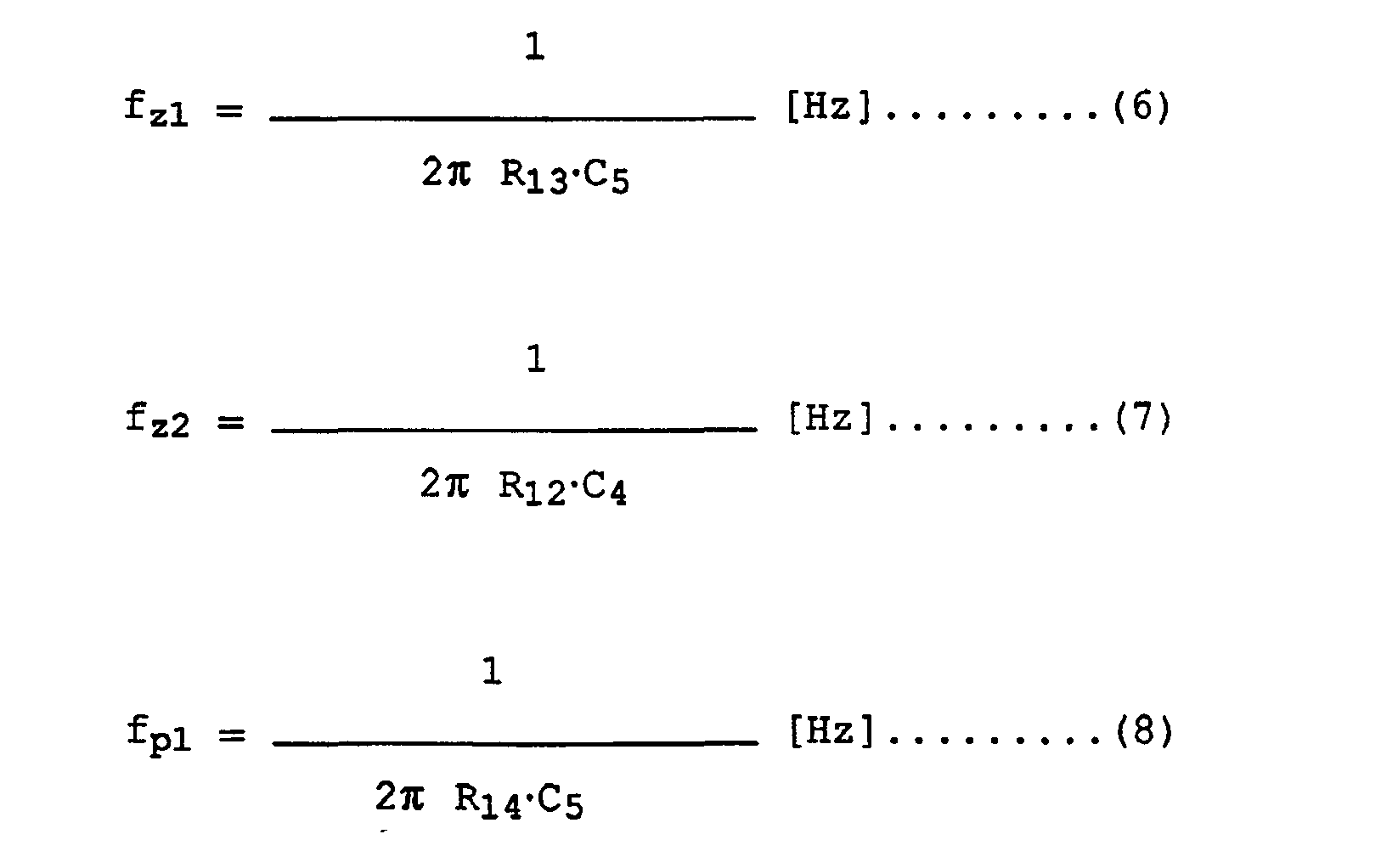
De versterkingsfactor van de foutversterker 56 wordtuitgedrukt door de hiernavolgende formule 9:The amplification factor of the error amplifier 56 is expressed by the following formula 9:

De foutversterker 56 bestuurt de frequentie van hetzaagtanduitgangssignaal van de VCO 54, en verhoogt deuitgangsfrequentie als er enige fluctuatie zoals dit is.Bijgevolg wordt de uitgangsfrequentie van de eerste comparator51 verhoogd, en wordt de frequentie van het uitgangsschakel-signaal door de frequentiedeler 55 ook verhoogd. Wanneer delogische keten 55 zich in een normale toestand bevindt,verschaft deze echter een uitgangssignaal van constantefrequentie.The error amplifier 56 controls the frequency of the sawtooth output signal of the VCO 54, and increases the output frequency if there is any fluctuation such as this. Therefore, the output frequency of the first comparator 51 is increased, and the frequency of the output switching signal by the frequency divider 55 is also increased. However, when logic circuit 55 is in a normal state, it provides a constant frequency output.
Samenvattend, als de aan de foutversterker 56 toegevoerdespanning toeneemt, dat wil zeggen het wisselspanningsniveau,stijgt het uitgangssignaal van de foutversterker 56. Alsgevolg hiervan neemt de zaagtandgolffrequentie toe, evenals deschakelfrequentie, waardoor het ingangsvermogen afneemt.In summary, as the voltage supplied to the error amplifier 56 increases, i.e. the AC voltage level, the output signal of the error amplifier 56 increases. As a result, the sawtooth wave frequency increases, as does the switching frequency, which decreases the input power.
In tegenstelling daarmee neemt het ingangsvermogen toewanneer de naar de foutversterker 56 toegevoerde spanningafneemt. Wanneer er derhalve een fluctuatie optreedt in debelasting Ro, zal een toename van de belasting Ro een toenameveroorzaken van het uitgangssignaal van de foutversterker 56om de uitgangsspanning te verlagen. Wanneer daarentegen debelasting Ro afneemt, stijgt de uitgangsspanning. Dat wilzeggen dat de uitgangsspanning constant geproduceerd wordt,zelfs in het geval van belastingfluctuaties.In contrast, the input power increases as the voltage supplied to the error amplifier 56 decreases. Therefore, when a fluctuation in the load Ro occurs, an increase in the load Ro will cause an increase in the output signal of the error amplifier 56 to decrease the output voltage. On the other hand, when the load Ro decreases, the output voltage increases. That is, the output voltage is produced constantly even in case of load fluctuations.
De fig. 12 en 13 illustreren voorkeursuitvoeringsvormenwaar de kenmerken van de on derhavige uitvinding zijntoegepast. Deze twee uitvoeringsvormen zijn vergelijkbaar metde keten van fig. 3.. Daarbij is echter in fig. 12 de uitgangs-keten vervangen door een hoge intensiteitontladingslamp (HID)en in fig. 13 is als belasting een ontladingslamp parallelverbonden met een condensator Cr van een resonantieketen. Eennaar de besturingsketen 5 teruggevoerd signaal is hierbijafhankelijk van de spanning van een weerstandsorgaan R30 datis verbonden met een secundaire spanning van de inductor Lrvan de resonantieketen.Figures 12 and 13 illustrate preferred embodiments where the features of the present invention have been applied. These two embodiments are similar to the circuit of FIG. 3. However, in FIG. 12 the output circuit is replaced by a high intensity discharge lamp (HID) and in FIG. 13 a discharge lamp is connected in parallel with a capacitor Cr of a resonant circuit as load. . A signal fed back to the control circuit 5 here depends on the voltage of a resistor R30 connected to a secondary voltage of the inductor Lr of the resonant circuit.
Deze voorkeursuitvoeringsvormen van de onderhavigeuitvinding zijn toepasbaar bij een elektronische stabilisator als een vermogenstoevoersysteem met een hoge vermogensfactor,een hoge efficiëntie en een hoge niveaudichtheid.These preferred embodiments of the present invention are applicable to an electronic stabilizer as a power supply system with a high power factor, high efficiency and high level density.
Volgens de onderhavige uitvinding zijn de totale ketenseenvoudiger dan een vermogensfactor-verbeterende keten waaromzettechniek van het "boosting"-type wordt gebruikt, zoalsgetoond in de fig. 2A en 2B, en de ingangsvermogensfactorwordt verhoogd door het verwijderen van dode hoek en dode tijdzoals getoond in fig. 2B teneinde voordelig te zijn inbetrouwbaarheid en kosten. Daarnaast is het mogelijk dat hethele systeem klein is van afmeting en licht in gewichtaangezien volgens de onderhavige uitvinding de resonanteomzetter wordt bestuurd.According to the present invention, the total circuits are simpler than a power factor-enhancing circuit using "boosting" type converting technique, as shown in Figs. 2A and 2B, and the input power factor is increased by removing blind spot and dead time as shown in Fig. 2B in order to be advantageous in reliability and cost. In addition, it is possible that the whole system is small in size and light in weight as the resonant converter is controlled in accordance with the present invention.
Als resultaat van het meten van de golfvormen van deingangsspanning en de ingangsstroom in de keten van deonderhavige uitvinding zoals getoond in fig. 3, kan de infig. 9G getoonde golfvorm worden verkregen.As a result of measuring the input voltage and input current waveforms in the circuit of the present invention as shown in Fig. 3, the infig. 9G waveform shown are obtained.
Vergeleken met de fig. 1B en 2B heeft deze golfvormgeen enkele vervorming. Bijgevolg is het aandeel aan hogefrequenties aanzienlijk verminderd in vergelijking met defig. 1B en 2B.Compared to FIGS. 1B and 2B, this waveform does not have any distortion. Consequently, the share of high frequencies is significantly reduced compared to defig. 1B and 2B.
Hoewel de onderhavige uitvinding is beschreven insamenhang met wat thans de meest praktische en de voorkeurverdienende uitvoeringsvormen worden beschouwd, zal hetduidelijk zijn dat de uitvinding niet tot de beschrevenuitvoeringsvormen is beperkt maar daarentegen bedoeld is omverscheidene modificaties en equivalente opstellingen tedekken die vallen binnen de geest en omvang van de bijgevoegdeconclusies.While the present invention has been described in conjunction with what are now considered to be the most practical and preferred embodiments, it will be understood that the invention is not limited to the described embodiments, but is intended rather to cover various modifications and equivalent arrangements that fall within the spirit and scope of the attached claims.
Claims (10)
Applications Claiming Priority (2)
| Application Number | Priority Date | Filing Date | Title |
|---|---|---|---|
| KR1019930006147A KR960010828B1 (en) | 1993-04-13 | 1993-04-13 | High Power Factor Power Supply |
| KR930006147 | 1993-04-13 |
Publications (3)
| Publication Number | Publication Date |
|---|---|
| NL9400580A true NL9400580A (en) | 1994-11-01 |
| NL194221B NL194221B (en) | 2001-05-01 |
| NL194221C NL194221C (en) | 2001-09-04 |
Family
ID=19353843
Family Applications (1)
| Application Number | Title | Priority Date | Filing Date |
|---|---|---|---|
| NL9400580A NL194221C (en) | 1993-04-13 | 1994-04-12 | Power supply system with high power factor. |
Country Status (5)
| Country | Link |
|---|---|
| US (1) | US5625538A (en) |
| JP (1) | JPH06327247A (en) |
| KR (1) | KR960010828B1 (en) |
| DE (1) | DE4412544A1 (en) |
| NL (1) | NL194221C (en) |
Families Citing this family (10)
| Publication number | Priority date | Publication date | Assignee | Title |
|---|---|---|---|---|
| GB2311387B (en) * | 1996-03-23 | 2000-03-22 | Oxford Magnet Tech | Regulated resonant converter |
| US5715155A (en) * | 1996-10-28 | 1998-02-03 | Norax Canada Inc. | Resonant switching power supply circuit |
| DE19751956A1 (en) * | 1997-11-24 | 1999-06-02 | Ilt International Licence Trad | Conversion of AC high voltage into DC low voltage |
| US6181116B1 (en) | 1998-05-22 | 2001-01-30 | Nmb U.S.A. Inc. | Power regulator |
| US6304046B1 (en) * | 1999-10-05 | 2001-10-16 | Samsung Electronics Co., Ltd. | Driving control circuit of a hood motor |
| DE60113166T2 (en) * | 2000-02-11 | 2006-06-08 | Siemens Magnet Technology Ltd., Oldbury, Bracknell | Regulated resonant converter |
| ATE354880T1 (en) | 2003-08-27 | 2007-03-15 | Fraunhofer Ges Forschung | CONTROL DEVICE FOR CONTROLLING A CHARGING SWITCH IN A SWITCHING REGULATOR AND METHOD FOR CONTROLLING A CHARGING SWITCH |
| WO2005039251A1 (en) * | 2003-10-17 | 2005-04-28 | Vicious Power Pty Ltd | Electronic power control for lamps |
| CN101820222B (en) * | 2010-06-18 | 2012-06-27 | 陶顺祝 | Full voltage range llc resonant converter and control method thereof |
| US8441810B2 (en) * | 2010-11-09 | 2013-05-14 | Flextronics Ap, Llc | Cascade power system architecture |
Citations (2)
| Publication number | Priority date | Publication date | Assignee | Title |
|---|---|---|---|---|
| US4513364A (en) * | 1980-08-14 | 1985-04-23 | Nilssen Ole K | Thermally controllable variable frequency inverter |
| EP0386980A2 (en) * | 1989-03-07 | 1990-09-12 | THORN EMI plc | Switched-mode regulator circuit |
Family Cites Families (5)
| Publication number | Priority date | Publication date | Assignee | Title |
|---|---|---|---|---|
| US4677366A (en) * | 1986-05-12 | 1987-06-30 | Pioneer Research, Inc. | Unity power factor power supply |
| CA2015281C (en) * | 1989-04-25 | 1995-08-29 | Minoru Maehara | Polarized electromagnetic relay |
| US5003454A (en) * | 1990-01-09 | 1991-03-26 | North American Philips Corporation | Power supply with improved power factor correction |
| US5315496A (en) * | 1990-01-29 | 1994-05-24 | Kabushiki Kaisha Toshiba | Current resonance converter having overload detecting function |
| US5371667A (en) * | 1993-06-14 | 1994-12-06 | Fuji Electrochemical Co., Ltd. | Electric power supply |
-
1993
- 1993-04-13 KR KR1019930006147A patent/KR960010828B1/en not_active Expired - Lifetime
-
1994
- 1994-04-12 NL NL9400580A patent/NL194221C/en not_active IP Right Cessation
- 1994-04-12 DE DE4412544A patent/DE4412544A1/en not_active Ceased
- 1994-04-13 JP JP6074755A patent/JPH06327247A/en active Pending
- 1994-04-13 US US08/227,353 patent/US5625538A/en not_active Expired - Lifetime
Patent Citations (2)
| Publication number | Priority date | Publication date | Assignee | Title |
|---|---|---|---|---|
| US4513364A (en) * | 1980-08-14 | 1985-04-23 | Nilssen Ole K | Thermally controllable variable frequency inverter |
| EP0386980A2 (en) * | 1989-03-07 | 1990-09-12 | THORN EMI plc | Switched-mode regulator circuit |
Non-Patent Citations (1)
| Title |
|---|
| CHOI H C ET AL: "HIGH FREQUENCY RESONANT AC/DC RECTIFIER WITH UNITY POWER FACTOR", ELECTRONICS LETTERS, vol. 28, no. 17, 13 August 1992 (1992-08-13), pages 1592 - 1594, XP000315865 * |
Also Published As
| Publication number | Publication date |
|---|---|
| DE4412544A1 (en) | 1994-10-20 |
| NL194221B (en) | 2001-05-01 |
| US5625538A (en) | 1997-04-29 |
| NL194221C (en) | 2001-09-04 |
| JPH06327247A (en) | 1994-11-25 |
| KR960010828B1 (en) | 1996-08-09 |
Similar Documents
| Publication | Publication Date | Title |
|---|---|---|
| JP3459142B2 (en) | Drive pulse output limiting circuit | |
| US20110038180A1 (en) | Resonant power converter with half bridge and full bridge operations and method for control thereof | |
| CN1166260C (en) | Light adjustable electronic ballast | |
| NL9400580A (en) | Power supply system with a high power factor. | |
| JP3664173B2 (en) | DC converter | |
| EP0553923B1 (en) | Inverter device | |
| JP3664012B2 (en) | Switching power supply | |
| EP0725475B1 (en) | DC converter with improved power factor | |
| JP2655673B2 (en) | Power supply | |
| JP2001197756A (en) | Power supply unit | |
| JP2003037973A (en) | Demagnetization reduction method and demagnetization reduction circuit in power converter | |
| US20020000923A1 (en) | Switching power supply circuit | |
| JPH0750987B2 (en) | Resonance type DC-DC converter control method | |
| JP2000236666A (en) | Power supply | |
| JP3740220B2 (en) | Fluorescent lamp lighting device | |
| JP3252540B2 (en) | Inverter device | |
| JP3396991B2 (en) | Power supply | |
| JP3329913B2 (en) | Power supply | |
| JP2655674B2 (en) | Power supply | |
| JP4379981B2 (en) | Power supply control circuit | |
| JP3543038B2 (en) | Inverter device | |
| JP3332295B2 (en) | Power supply | |
| JP3285231B2 (en) | Discharge lamp lighting device | |
| JP3562251B2 (en) | Power supply | |
| JP3404880B2 (en) | Inverter device |
Legal Events
| Date | Code | Title | Description |
|---|---|---|---|
| BA | A request for search or an international-type search has been filed | ||
| BB | A search report has been drawn up | ||
| BC | A request for examination has been filed | ||
| SNR | Assignments of patents or rights arising from examined patent applications |
Owner name: FAIRCHILD KOREA SEMICONDUCTOR LTD. |
|
| V4 | Discontinued because of reaching the maximum lifetime of a patent |
Effective date: 20140412 |