KR20250038851A - Semiconductor package comprising BSPDN layer - Google Patents
Semiconductor package comprising BSPDN layer Download PDFInfo
- Publication number
- KR20250038851A KR20250038851A KR1020230120849A KR20230120849A KR20250038851A KR 20250038851 A KR20250038851 A KR 20250038851A KR 1020230120849 A KR1020230120849 A KR 1020230120849A KR 20230120849 A KR20230120849 A KR 20230120849A KR 20250038851 A KR20250038851 A KR 20250038851A
- Authority
- KR
- South Korea
- Prior art keywords
- semiconductor chip
- substrate
- semiconductor
- mold film
- redistribution
- Prior art date
- Legal status (The legal status is an assumption and is not a legal conclusion. Google has not performed a legal analysis and makes no representation as to the accuracy of the status listed.)
- Pending
Links
Images


Classifications
-
- H10W70/685—
-
- H—ELECTRICITY
- H01—ELECTRIC ELEMENTS
- H01L—SEMICONDUCTOR DEVICES NOT COVERED BY CLASS H10
- H01L25/00—Assemblies consisting of a plurality of semiconductor or other solid state devices
- H01L25/03—Assemblies consisting of a plurality of semiconductor or other solid state devices all the devices being of a type provided for in a single subclass of subclasses H10B, H10D, H10F, H10H, H10K or H10N, e.g. assemblies of rectifier diodes
- H01L25/04—Assemblies consisting of a plurality of semiconductor or other solid state devices all the devices being of a type provided for in a single subclass of subclasses H10B, H10D, H10F, H10H, H10K or H10N, e.g. assemblies of rectifier diodes the devices not having separate containers
- H01L25/065—Assemblies consisting of a plurality of semiconductor or other solid state devices all the devices being of a type provided for in a single subclass of subclasses H10B, H10D, H10F, H10H, H10K or H10N, e.g. assemblies of rectifier diodes the devices not having separate containers the devices being of a type provided for in group H10D89/00
- H01L25/0657—Stacked arrangements of devices
-
- H—ELECTRICITY
- H01—ELECTRIC ELEMENTS
- H01L—SEMICONDUCTOR DEVICES NOT COVERED BY CLASS H10
- H01L23/00—Details of semiconductor or other solid state devices
- H01L23/28—Encapsulations, e.g. encapsulating layers, coatings, e.g. for protection
- H01L23/31—Encapsulations, e.g. encapsulating layers, coatings, e.g. for protection characterised by the arrangement or shape
- H01L23/3157—Partial encapsulation or coating
- H01L23/3185—Partial encapsulation or coating the coating covering also the sidewalls of the semiconductor body
-
- H—ELECTRICITY
- H01—ELECTRIC ELEMENTS
- H01L—SEMICONDUCTOR DEVICES NOT COVERED BY CLASS H10
- H01L23/00—Details of semiconductor or other solid state devices
- H01L23/48—Arrangements for conducting electric current to or from the solid state body in operation, e.g. leads, terminal arrangements ; Selection of materials therefor
- H01L23/481—Internal lead connections, e.g. via connections, feedthrough structures
-
- H—ELECTRICITY
- H01—ELECTRIC ELEMENTS
- H01L—SEMICONDUCTOR DEVICES NOT COVERED BY CLASS H10
- H01L23/00—Details of semiconductor or other solid state devices
- H01L23/48—Arrangements for conducting electric current to or from the solid state body in operation, e.g. leads, terminal arrangements ; Selection of materials therefor
- H01L23/482—Arrangements for conducting electric current to or from the solid state body in operation, e.g. leads, terminal arrangements ; Selection of materials therefor consisting of lead-in layers inseparably applied to the semiconductor body (electrodes)
-
- H—ELECTRICITY
- H01—ELECTRIC ELEMENTS
- H01L—SEMICONDUCTOR DEVICES NOT COVERED BY CLASS H10
- H01L23/00—Details of semiconductor or other solid state devices
- H01L23/48—Arrangements for conducting electric current to or from the solid state body in operation, e.g. leads, terminal arrangements ; Selection of materials therefor
- H01L23/488—Arrangements for conducting electric current to or from the solid state body in operation, e.g. leads, terminal arrangements ; Selection of materials therefor consisting of soldered or bonded constructions
- H01L23/498—Leads, i.e. metallisations or lead-frames on insulating substrates, e.g. chip carriers
- H01L23/49811—Additional leads joined to the metallisation on the insulating substrate, e.g. pins, bumps, wires, flat leads
- H01L23/49816—Spherical bumps on the substrate for external connection, e.g. ball grid arrays [BGA]
-
- H—ELECTRICITY
- H01—ELECTRIC ELEMENTS
- H01L—SEMICONDUCTOR DEVICES NOT COVERED BY CLASS H10
- H01L23/00—Details of semiconductor or other solid state devices
- H01L23/52—Arrangements for conducting electric current within the device in operation from one component to another, i.e. interconnections, e.g. wires, lead frames
- H01L23/522—Arrangements for conducting electric current within the device in operation from one component to another, i.e. interconnections, e.g. wires, lead frames including external interconnections consisting of a multilayer structure of conductive and insulating layers inseparably formed on the semiconductor body
- H01L23/528—Layout of the interconnection structure
- H01L23/5283—Cross-sectional geometry
-
- H—ELECTRICITY
- H01—ELECTRIC ELEMENTS
- H01L—SEMICONDUCTOR DEVICES NOT COVERED BY CLASS H10
- H01L23/00—Details of semiconductor or other solid state devices
- H01L23/52—Arrangements for conducting electric current within the device in operation from one component to another, i.e. interconnections, e.g. wires, lead frames
- H01L23/522—Arrangements for conducting electric current within the device in operation from one component to another, i.e. interconnections, e.g. wires, lead frames including external interconnections consisting of a multilayer structure of conductive and insulating layers inseparably formed on the semiconductor body
- H01L23/528—Layout of the interconnection structure
- H01L23/5286—Arrangements of power or ground buses
-
- H—ELECTRICITY
- H01—ELECTRIC ELEMENTS
- H01L—SEMICONDUCTOR DEVICES NOT COVERED BY CLASS H10
- H01L23/00—Details of semiconductor or other solid state devices
- H01L23/52—Arrangements for conducting electric current within the device in operation from one component to another, i.e. interconnections, e.g. wires, lead frames
- H01L23/522—Arrangements for conducting electric current within the device in operation from one component to another, i.e. interconnections, e.g. wires, lead frames including external interconnections consisting of a multilayer structure of conductive and insulating layers inseparably formed on the semiconductor body
- H01L23/532—Arrangements for conducting electric current within the device in operation from one component to another, i.e. interconnections, e.g. wires, lead frames including external interconnections consisting of a multilayer structure of conductive and insulating layers inseparably formed on the semiconductor body characterised by the materials
- H01L23/5329—Insulating materials
- H01L23/53295—Stacked insulating layers
-
- H—ELECTRICITY
- H01—ELECTRIC ELEMENTS
- H01L—SEMICONDUCTOR DEVICES NOT COVERED BY CLASS H10
- H01L23/00—Details of semiconductor or other solid state devices
- H01L23/52—Arrangements for conducting electric current within the device in operation from one component to another, i.e. interconnections, e.g. wires, lead frames
- H01L23/538—Arrangements for conducting electric current within the device in operation from one component to another, i.e. interconnections, e.g. wires, lead frames the interconnection structure between a plurality of semiconductor chips being formed on, or in, insulating substrates
- H01L23/5389—Arrangements for conducting electric current within the device in operation from one component to another, i.e. interconnections, e.g. wires, lead frames the interconnection structure between a plurality of semiconductor chips being formed on, or in, insulating substrates the chips being integrally enclosed by the interconnect and support structures
-
- H—ELECTRICITY
- H01—ELECTRIC ELEMENTS
- H01L—SEMICONDUCTOR DEVICES NOT COVERED BY CLASS H10
- H01L25/00—Assemblies consisting of a plurality of semiconductor or other solid state devices
- H01L25/03—Assemblies consisting of a plurality of semiconductor or other solid state devices all the devices being of a type provided for in a single subclass of subclasses H10B, H10D, H10F, H10H, H10K or H10N, e.g. assemblies of rectifier diodes
- H01L25/10—Assemblies consisting of a plurality of semiconductor or other solid state devices all the devices being of a type provided for in a single subclass of subclasses H10B, H10D, H10F, H10H, H10K or H10N, e.g. assemblies of rectifier diodes the devices having separate containers
- H01L25/105—Assemblies consisting of a plurality of semiconductor or other solid state devices all the devices being of a type provided for in a single subclass of subclasses H10B, H10D, H10F, H10H, H10K or H10N, e.g. assemblies of rectifier diodes the devices having separate containers the devices being integrated devices of class H10
-
- H—ELECTRICITY
- H01—ELECTRIC ELEMENTS
- H01L—SEMICONDUCTOR DEVICES NOT COVERED BY CLASS H10
- H01L25/00—Assemblies consisting of a plurality of semiconductor or other solid state devices
- H01L25/18—Assemblies consisting of a plurality of semiconductor or other solid state devices the devices being of the types provided for in two or more different main groups of the same subclass of H10B, H10D, H10F, H10H, H10K or H10N
-
- H10P72/74—
-
- H10W20/20—
-
- H10W20/40—
-
- H10W20/42—
-
- H10W20/427—
-
- H10W20/435—
-
- H10W20/47—
-
- H10W70/09—
-
- H10W70/611—
-
- H10W70/614—
-
- H10W70/635—
-
- H10W74/117—
-
- H10W74/141—
-
- H10W90/00—
-
- H10W90/401—
-
- H10W90/701—
-
- H10P72/7424—
-
- H10W70/60—
-
- H10W70/652—
-
- H10W72/823—
-
- H10W72/884—
-
- H10W74/15—
-
- H10W90/297—
-
- H10W90/722—
-
- H10W90/724—
-
- H10W90/734—
-
- H10W90/754—
-
- H10W90/794—
Landscapes
- Engineering & Computer Science (AREA)
- Microelectronics & Electronic Packaging (AREA)
- Power Engineering (AREA)
- Physics & Mathematics (AREA)
- Computer Hardware Design (AREA)
- Condensed Matter Physics & Semiconductors (AREA)
- General Physics & Mathematics (AREA)
- Geometry (AREA)
- Production Of Multi-Layered Print Wiring Board (AREA)
Abstract
반도체 패키지 및 이의 제조 방법을 제공한다. 본 발명의 개념에 따른 반도체 패키지는 제1 재배선 기판; 상기 제1 재배선 기판 상의 제1 반도체 칩; 상기 제1 재배선 기판과 상기 제1 반도체 칩을 덮는 제1 몰드막; 상기 제1 몰드막을 관통하여 상기 제1 재배선 기판과 접하는 복수개의 제1 도전 기둥들; 상기 제1 몰드막 상의 제2 재배선 기판; 상기 제2 재배선 기판 상의 제2 반도체 칩; 상기 제2 재배선 기판과 상기 제2 반도체 칩을 덮는 제2 몰드막; 상기 제2 몰드막을 관통하여 상기 제2 재배선 기판과 접하는 복수개의 제2 도전 기둥들; 및 상기 제2 몰드막 상의 제3 재배선 기판을 포함하되, 상기 제1 반도체 칩은 제1 관통 비아를 포함하고, 상기 제2 반도체 칩은 후면 파워 전송 네트워크층을 포함한다.A semiconductor package and a method for manufacturing the same are provided. A semiconductor package according to the concept of the present invention comprises: a first redistribution substrate; a first semiconductor chip on the first redistribution substrate; a first mold film covering the first redistribution substrate and the first semiconductor chip; a plurality of first conductive pillars penetrating the first mold film and contacting the first redistribution substrate; a second redistribution substrate on the first mold film; a second semiconductor chip on the second redistribution substrate; a second mold film covering the second redistribution substrate and the second semiconductor chip; a plurality of second conductive pillars penetrating the second mold film and contacting the second redistribution substrate; and a third redistribution substrate on the second mold film, wherein the first semiconductor chip includes a first through via and the second semiconductor chip includes a backside power transmission network layer.
Description
본 발명은 반도체 패키지에 관한 것으로, 더욱 상세하게는 BSPDN(Backside Power Delivery Network) 층을 포함하는 팬 아웃 웨이퍼 레벨 패키지(Fan-out Wafer Level Package, FOWLP)에 관한 것이다.The present invention relates to a semiconductor package, and more particularly, to a fan-out wafer level package (FOWLP) including a backside power delivery network (BSPDN) layer.
반도체 패키지는 집적회로 칩을 전자제품에 사용하기 적합한 형태로 구현한 것이다. 통상적으로 반도체 패키지는 인쇄회로기판 상에 반도체 다이를 실장하고 본딩 와이어 내지 범프를 이용하여 이들을 전기적으로 연결하는 것이 일반적이다. 전자 산업의 발달로 반도체 패키지의 신뢰성 및 내구성 향상을 위한 다양한 연구가 진행되고 있다.A semiconductor package is an implementation of an integrated circuit chip in a form suitable for use in electronic products. Typically, a semiconductor package is made by mounting a semiconductor die on a printed circuit board and electrically connecting them using bonding wires or bumps. With the development of the electronics industry, various studies are being conducted to improve the reliability and durability of semiconductor packages.
본 발명이 해결하고자 하는 과제는 파워 효율과 발열 성능이 개선된 반도체 패키지를 제공하는데 있다.The problem to be solved by the present invention is to provide a semiconductor package with improved power efficiency and heat generation performance.
상기 과제를 달성하기 위한 본 발명의 개념에 따른 반도체 패키지는 제1 재배선 기판; 상기 제1 재배선 기판 상의 제1 반도체 칩; 상기 제1 재배선 기판과 상기 제1 반도체 칩을 덮는 제1 몰드막; 상기 제1 몰드막을 관통하여 상기 제1 재배선 기판과 접하는 복수개의 제1 도전 기둥들; 상기 제1 몰드막 상의 제2 재배선 기판; 상기 제2 재배선 기판 상의 제2 반도체 칩; 상기 제2 재배선 기판과 상기 제2 반도체 칩을 덮는 제2 몰드막; 상기 제2 몰드막을 관통하여 상기 제2 재배선 기판과 접하는 복수개의 제2 도전 기둥들; 및 상기 제2 몰드막 상의 제3 재배선 기판을 포함하되, 상기 제1 반도체 칩은 제1 관통 비아를 포함하고, 상기 제2 반도체 칩은 후면 파워 전송 네트워크층을 포함한다.According to the concept of the present invention for achieving the above object, a semiconductor package comprises: a first redistribution substrate; a first semiconductor chip on the first redistribution substrate; a first mold film covering the first redistribution substrate and the first semiconductor chip; a plurality of first conductive pillars penetrating the first mold film and making contact with the first redistribution substrate; a second redistribution substrate on the first mold film; a second semiconductor chip on the second redistribution substrate; a second mold film covering the second redistribution substrate and the second semiconductor chip; a plurality of second conductive pillars penetrating the second mold film and making contact with the second redistribution substrate; and a third redistribution substrate on the second mold film, wherein the first semiconductor chip includes a first through via, and the second semiconductor chip includes a backside power transmission network layer.
본 발명의 일 양태에 따른 반도체 패키지는 제1 서브 패키지; 및 상기 제1 서브 패키지 상의 제2 서브 패키지를 포함하되, 상기 제1 서브 패키지는: 제1 재배선 기판; 상기 재배선 기판 상의 제1 반도체 칩; 상기 제1 재배선 기판과 상기 제1 반도체 칩을 덮는 제1 몰드막; 상기 제1 몰드막을 관통하여 상기 제1 재배선 기판과 접하는 복수개의 제1 도전 기둥들; 상기 제1 몰드막 상의 제2 재배선 기판; 상기 제2 재배선 기판 상의 제2 반도체 칩; 상기 제2 재배선 기판과 상기 제2 반도체 칩을 덮는 제2 몰드막; 상기 제2 몰드막을 관통하여 상기 제2 재배선 기판과 접하는 복수개의 제2 도전 기둥들; 및 상기 제2 몰드막 상의 제3 재배선 기판을 포함하되, 상기 제1 반도체 칩은 제1 관통 비아를 포함하고, 상기 제2 반도체 칩은 후면 파워 전송 네트워크층을 포함하고, 상기 제1 반도체 칩은 제1 방향으로 제1 폭을 가지고, 상기 제2 반도체 칩은 상기 제1 방향으로 제2 폭을 가지고, 상기 제2 폭은 상기 제1 폭보다 크다.According to one aspect of the present invention, a semiconductor package comprises: a first sub-package; and a second sub-package on the first sub-package, wherein the first sub-package comprises: a first redistribution substrate; a first semiconductor chip on the redistribution substrate; a first mold film covering the first redistribution substrate and the first semiconductor chip; a plurality of first conductive pillars penetrating the first mold film and making contact with the first redistribution substrate; a second redistribution substrate on the first mold film; a second semiconductor chip on the second redistribution substrate; a second mold film covering the second redistribution substrate and the second semiconductor chip; a plurality of second conductive pillars penetrating the second mold film and making contact with the second redistribution substrate; And a third rewiring substrate on the second mold film, wherein the first semiconductor chip includes a first through via, the second semiconductor chip includes a rear power transmission network layer, the first semiconductor chip has a first width in a first direction, the second semiconductor chip has a second width in the first direction, and the second width is larger than the first width.
본 발명의 다른 양태에 따른 반도체 패키지는 제1 재배선 기판; 상기 제1 재배선 기판 상의 제1 반도체 칩; 상기 제1 재배선 기판과 상기 제1 반도체 칩을 덮는 제1 몰드막; 상기 제1 몰드막을 관통하여 상기 제1 재배선 기판과 접하는 복수개의 제1 도전 기둥들; 상기 제1 몰드막 상의 제2 재배선 기판; 상기 제2 재배선 기판 상의 제2 반도체 칩; 상기 제2 재배선 기판과 상기 제2 반도체 칩을 덮는 제2 몰드막; 상기 제2 몰드막을 관통하여 상기 제2 재배선 기판과 접하는 복수개의 제2 도전 기둥들; 및 상기 제2 몰드막 상의 제3 재배선 기판을 포함하되, 상기 제1 반도체 칩은 제1 관통 비아를 포함하고, 상기 제1 반도체 칩의 하면은 상기 제1 재배선 기판과 접하고, 상기 제2 반도체 칩은 후면 파워 전송 네트워크층을 포함하고, 상기 제1 반도체 칩은 제1 방향으로 제1 폭을 가지고, 상기 제2 반도체 칩은 상기 제1 방향으로 제2 폭을 가지고, 상기 제2 폭은 상기 제1 폭보다 크다.According to another aspect of the present invention, a semiconductor package comprises: a first redistribution substrate; a first semiconductor chip on the first redistribution substrate; a first mold film covering the first redistribution substrate and the first semiconductor chip; a plurality of first conductive pillars penetrating the first mold film and making contact with the first redistribution substrate; a second redistribution substrate on the first mold film; a second semiconductor chip on the second redistribution substrate; a second mold film covering the second redistribution substrate and the second semiconductor chip; a plurality of second conductive pillars penetrating the second mold film and making contact with the second redistribution substrate; And a third redistribution substrate on the second mold film, wherein the first semiconductor chip includes a first through via, a lower surface of the first semiconductor chip is in contact with the first redistribution substrate, and the second semiconductor chip includes a rear power transmission network layer, wherein the first semiconductor chip has a first width in a first direction, and the second semiconductor chip has a second width in the first direction, and the second width is larger than the first width.
본 발명의 개념에 따른 반도체 패키지에서는 후면 파워 전송 네트워크층을 포함하는 로직 칩에 반도체 칩을 웨이퍼 온 웨이퍼(Wafer on Wafer) 방식으로 본딩하여 칩렛(Chiplet) 구조의 반도체 패키지를 제공한다. 파워 기능을 담당하는 파워 배선을 로직 칩의 후면에 배치하여 반도체 패키지의 집적도가 향상될 수 있다. 웨이퍼 온 웨이퍼 본딩된 반도체 칩들의 크기가 같음으로써 조립 과정에서 수율이 향상된 반도체 패키지가 제공될 수 있다. 제1 재배선 기판에 실장된 반도체 칩보다 크기가 크고 발열이 많은 칩렛 구조의 반도체 칩을 제2 재배선 기판에 실장함으로써 반도체 패키지의 발열 성능을 향상시킬 수 있다.In a semiconductor package according to the concept of the present invention, a semiconductor chip including a rear power transmission network layer is bonded to a logic chip in a wafer-on-wafer manner to provide a semiconductor package having a chiplet structure. Power wiring in charge of a power function is arranged on the rear of the logic chip, so that the integration degree of the semiconductor package can be improved. Since the sizes of the wafer-on-wafer bonded semiconductor chips are the same, a semiconductor package having an improved yield during the assembly process can be provided. The heat dissipation performance of the semiconductor package can be improved by mounting a semiconductor chip having a chiplet structure that is larger in size and generates more heat than the semiconductor chip mounted on the first redistribution substrate on the second redistribution substrate.
도 1은 본 발명의 실시예들에 따른 반도체 패키지의 단면도이다.
도 2는 도 1의 ‘P1’ 부분을 확대한 도면이다.
도 3은 본 발명의 실시예들에 따른 반도체 패키지의 단면도이다.
도 4a 내지 도 4e는 도 1의 제2 반도체 칩을 제조하는 과정을 순차적으로 나타내는 단면도들이다.
도 5a 내지 도 5f는 도 1의 반도체 패키지를 제조하는 과정을 순차적으로 나타내는 단면도들이다.
도 6은 본 발명의 실시예들에 따른 반도체 패키지의 단면도이다.FIG. 1 is a cross-sectional view of a semiconductor package according to embodiments of the present invention.
Figure 2 is an enlarged drawing of the 'P1' portion of Figure 1.
FIG. 3 is a cross-sectional view of a semiconductor package according to embodiments of the present invention.
FIGS. 4A to 4E are cross-sectional views sequentially showing a process for manufacturing the second semiconductor chip of FIG. 1.
FIGS. 5A to 5F are cross-sectional views sequentially showing a process for manufacturing the semiconductor package of FIG. 1.
FIG. 6 is a cross-sectional view of a semiconductor package according to embodiments of the present invention.
이하, 본 발명을 보다 구체적으로 설명하기 위하여 본 발명에 따른 실시예들을 첨부 도면을 참조하면서 보다 상세하게 설명하고자 한다.Hereinafter, in order to explain the present invention more specifically, embodiments according to the present invention will be described in more detail with reference to the attached drawings.
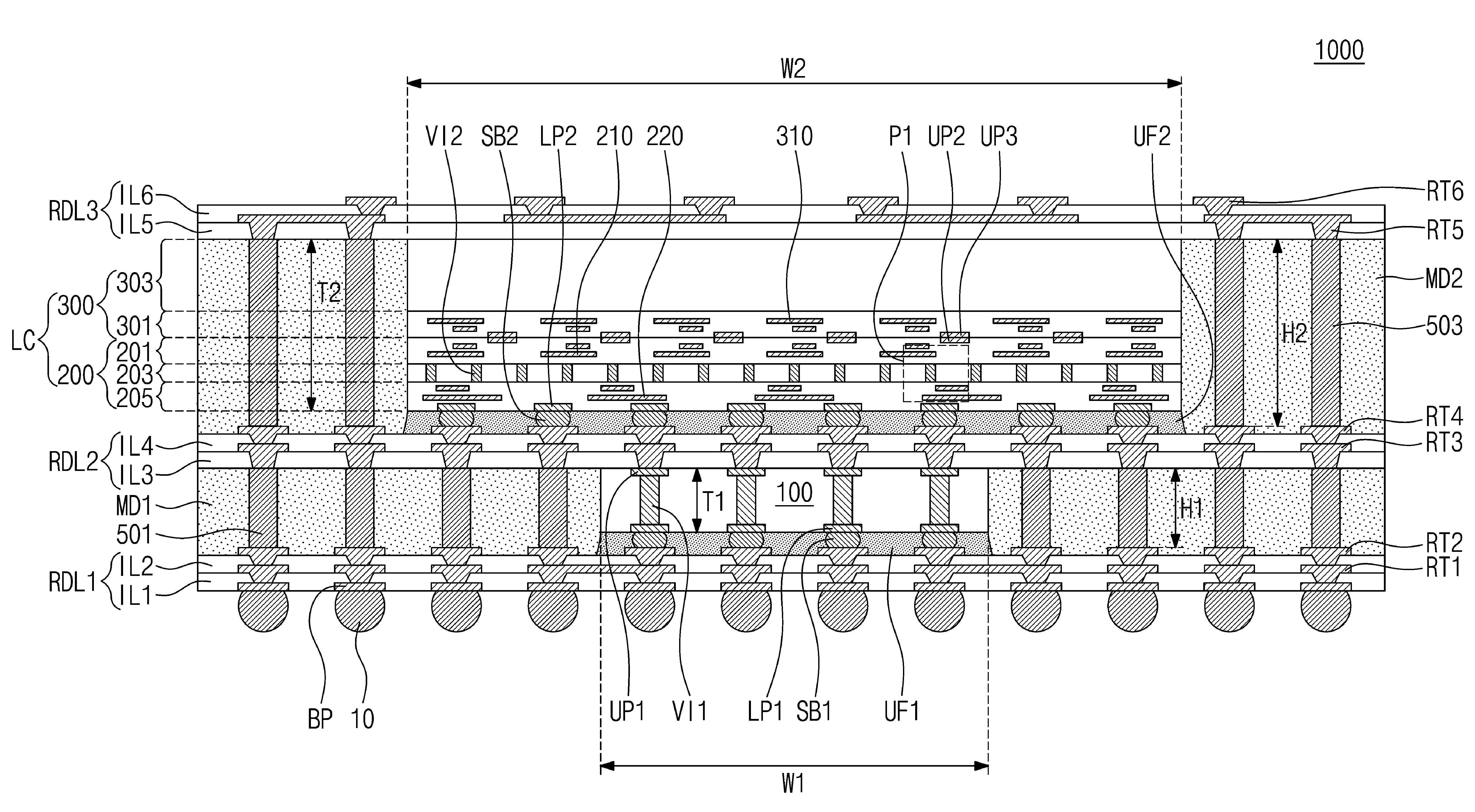
도 1은 본 발명의 실시예들에 따른 반도체 패키지의 단면도이다. 도 2는 도 1의 ‘P1’ 부분을 확대한 도면이다.Fig. 1 is a cross-sectional view of a semiconductor package according to embodiments of the present invention. Fig. 2 is an enlarged view of a portion ‘P1’ of Fig. 1.
도 1을 참조하면, 본 예에 따른 반도체 패키지(1000)는 칩 라스트(Chip last)형 팬아웃 웨이퍼 레벨 패키지(Fan-out Wafer Level Package, FOWLP) 형태를 가질 수 있다. 반도체 패키지(1000)는 제1 재배선 기판(RDL1)과 이 위에 실장되는 제1 반도체 칩(100)을 포함할 수 있다. 제1 재배선 기판(RDL1)과 제1 반도체 칩(100)은 제1 몰드막(MD1)으로 덮일 수 있다. 제1 몰드막(MD1) 상에 제2 재배선 기판(RDL2)이 배치될 수 있다. 제1 도전 기둥들(501)은 제1 몰드막(MD1)을 관통하여 제1 재배선 기판(RDL1)과 제2 재배선 기판(RDL2)을 전기적으로 연결시킬 수 있다. 제2 재배선 기판(RDL2) 위에 제2 반도체 칩(LC)이 실장될 수 있다. 제2 재배선 기판(RDL2)과 제2 반도체 칩(LC)은 제2 몰드막(MD2)으로 덮일 수 있다. 제2 몰드막(MD2) 상에 제3 재배선 기판(RDL3)이 배치될 수 있다. 제2 도전 기둥들(503)은 제2 몰드막(MD2)을 관통하여 제2 재배선 기판(RDL2)과 제3 재배선 기판(RDL3)을 전기적으로 연결시킬 수 있다. Referring to FIG. 1, a semiconductor package (1000) according to the present example may have a chip last type fan-out wafer level package (FOWLP) form. The semiconductor package (1000) may include a first redistribution substrate (RDL1) and a first semiconductor chip (100) mounted thereon. The first redistribution substrate (RDL1) and the first semiconductor chip (100) may be covered with a first mold film (MD1). A second redistribution substrate (RDL2) may be disposed on the first mold film (MD1). First conductive pillars (501) may electrically connect the first redistribution substrate (RDL1) and the second redistribution substrate (RDL2) by penetrating the first mold film (MD1). A second semiconductor chip (LC) may be mounted on the second redistribution substrate (RDL2). The second redistribution substrate (RDL2) and the second semiconductor chip (LC) may be covered with a second mold film (MD2). A third redistribution substrate (RDL3) may be placed on the second mold film (MD2). The second conductive pillars (503) may electrically connect the second redistribution substrate (RDL2) and the third redistribution substrate (RDL3) by penetrating the second mold film (MD2).
제1 재배선 기판(RDL1)은 차례로 적층된 제1 및 제2 재배선 절연막들(IL1, IL2)을 포함할 수 있다. 그러나 이에 한정되지 않고 제1 재배선 기판(RDL1)은 3층 이상의 재배선 절연막들로 이루어질 수 있다. 제1 및 제2 재배선 절연막들(IL1, IL2)은 각각 감광성 절연(Photo Imageable Dielectric: PID)막을 포함할 수 있다. 또는 제1 및 제2 재배선 절연막들(IL1, IL2)은 각각 경화성 절연막(Ajinomoto build-up film: ABF)을 포함할 수 있다. 제1 재배선 절연막(IL1)과 제2 재배선 절연막(IL2) 사이에 제1 재배선 패턴(RT1)이 개재될 수 있다. 제2 재배선 절연막(IL2)과 제1 몰드막(MD1) 사이에 제2 재배선 패턴(RT2)이 개재될 수 있다. The first redistribution substrate (RDL1) may include first and second redistribution insulating films (IL1, IL2) that are sequentially laminated. However, the present invention is not limited thereto, and the first redistribution substrate (RDL1) may be formed of three or more layers of redistribution insulating films. The first and second redistribution insulating films (IL1, IL2) may each include a photo-imageable dielectric (PID) film. Alternatively, the first and second redistribution insulating films (IL1, IL2) may each include a curable insulating film (Ajinomoto build-up film: ABF). A first redistribution pattern (RT1) may be interposed between the first redistribution insulating film (IL1) and the second redistribution insulating film (IL2). A second redistribution pattern (RT2) may be interposed between the second redistribution insulating film (IL2) and the first mold film (MD1).
제1 재배선 절연막(IL1)의 하면에 하부 본딩 패드들(BP)이 배치될 수 있다. 하부 본딩 패드들(BP)은 제1 재배선 패턴(RT1)과 접할 수 있다. 제1 및 제2 재배선 패턴들(RT1, RT2)과 하부 본딩 패드들(BP)은 각각 구리, 알루미늄, 텅스텐, 니켈, 금, 주석, 티타늄 중 적어도 하나를 포함할 수 있다. 도시하지는 않았지만, 제1 및 제2 재배선 패턴들(RT1, RT2)의 측벽들과 하부면들은 베리어/시드막으로 덮일 수 있다. 상기 베리어/시드막은 차례로 적층된 베리어막과 시드막을 포함할 수 있다. 상기 베리어막은 금속 질화막을 포함할 수 있다. 상기 시드막은 제1 및 제2 재배선 패턴들(RT1, RT2)과 동일한 금속을 포함할 수 있다. 하부 본딩 패드들(BP)에 외부 연결 부재들(10)이 본딩될 수 있다. 외부 연결 부재들(10)은 솔더볼, 도전 범프 및 도전 필라 중 적어도 하나를 포함할 수 있다. 외부 연결 부재들(10)은 주석, 납, 은, 구리, 알루미늄, 금, 니켈 중 적어도 하나를 포함할 수 있다.Lower bonding pads (BP) may be arranged on a lower surface of a first redistribution insulating film (IL1). The lower bonding pads (BP) may be in contact with the first redistribution pattern (RT1). The first and second redistribution patterns (RT1, RT2) and the lower bonding pads (BP) may each include at least one of copper, aluminum, tungsten, nickel, gold, tin, and titanium. Although not illustrated, sidewalls and lower surfaces of the first and second redistribution patterns (RT1, RT2) may be covered with a barrier/seed film. The barrier/seed film may include a barrier film and a seed film that are sequentially stacked. The barrier film may include a metal nitride film. The seed film may include the same metal as the first and second redistribution patterns (RT1, RT2). External connection members (10) may be bonded to the lower bonding pads (BP). The external connecting members (10) may include at least one of a solder ball, a conductive bump, and a conductive pillar. The external connecting members (10) may include at least one of tin, lead, silver, copper, aluminum, gold, and nickel.
제1 반도체 칩(100)은 입출력 단자들을 포함할 수 있다. 제1 반도체 칩(100)은 제2 반도체 칩(LC)과 외부의 컨트롤러 간의 인터페이스 회로로서 동작할 수 있다. 제1 반도체 칩(100)은 상기 입출력 단자들을 통해서 제2 반도체 칩(LC)으로부터 출력되는 데이터를 외부의 컨트롤러로 전송할 수 있다. 도시하지는 않았지만 제1 반도체 칩(100)은 제1 기판, 층간절연막 및 내부 배선을 포함할 수 있다.The first semiconductor chip (100) may include input/output terminals. The first semiconductor chip (100) may operate as an interface circuit between the second semiconductor chip (LC) and an external controller. The first semiconductor chip (100) may transmit data output from the second semiconductor chip (LC) to the external controller through the input/output terminals. Although not illustrated, the first semiconductor chip (100) may include a first substrate, an interlayer insulating film, and internal wiring.
제1 반도체 칩(100)은 제1 관통 비아(VI1)를 포함할 수 있다. 제1 관통 비아(VI1)는 제1 반도체 칩(100)의 상기 제1 기판을 관통할 수 있다. 도시하지는 않았지만 제1 관통 비아(VI1)와 상기 제1 기판 사이에는 제1 관통 절연막이 개재될 수 있다. 제1 관통 비아(VI1)는 구리, 알루미늄, 텅스텐과 같은 금속을 포함할 수 있다. 제1 반도체 칩(100)은 제1 관통 비아(VI1)를 통해 제1 재배선 기판 및 제2 재배선 기판과 전기적으로 연결될 수 있다. The first semiconductor chip (100) may include a first through-via (VI1). The first through-via (VI1) may penetrate the first substrate of the first semiconductor chip (100). Although not illustrated, a first through-insulating film may be interposed between the first through-via (VI1) and the first substrate. The first through-via (VI1) may include a metal such as copper, aluminum, or tungsten. The first semiconductor chip (100) may be electrically connected to the first redistribution substrate and the second redistribution substrate through the first through-via (VI1).
제1 반도체 칩(100)의 상면에 제1 상부 도전 패드들(UP1) 그리고 하면에 제1 하부 도전 패드들(LP1)이 배치될 수 있다. 제1 상부 도전 패드들(UP1)과 제1 하부 도전 패드들(LP1)은 각각 제1 관통 비아(VI1)와 연결될 수 있다. First upper conductive pads (UP1) may be arranged on the upper surface of the first semiconductor chip (100) and first lower conductive pads (LP1) may be arranged on the lower surface. The first upper conductive pads (UP1) and the first lower conductive pads (LP1) may each be connected to a first through-via (VI1).
제1 반도체 칩(100)은 제1 내부 연결 부재들(SB1)에 의해 플립칩 본딩 방식으로 제1 재배선 기판(RDL1)에 연결될 수 있다. 제1 내부 연결 부재들(SB1)은 제1 반도체 칩(100)의 제1 하부 도전 패드들(LP1)과 이에 대응하는 제2 재배선 패턴들(RT2)을 각각 전기적으로 연결시킬 수 있다. 제1 내부 연결 부재들(SB1)은 솔더볼, 도전 범프, 도전 필라 중 적어도 하나를 포함할 수 있다. 제1 내부 연결 부재들(SB1)은 주석, 납, 은, 알루미늄, 금, 니켈 중 적어도 하나를 포함할 수 있다.A first semiconductor chip (100) may be connected to a first redistribution substrate (RDL1) by a flip-chip bonding method by first internal connection members (SB1). The first internal connection members (SB1) may electrically connect first lower conductive pads (LP1) of the first semiconductor chip (100) and second redistribution patterns (RT2) corresponding thereto, respectively. The first internal connection members (SB1) may include at least one of a solder ball, a conductive bump, and a conductive pillar. The first internal connection members (SB1) may include at least one of tin, lead, silver, aluminum, gold, and nickel.
제1 반도체 칩(100)과 제1 재배선 기판(RDL1) 사이에 제1 언더필(UF1)이 개재될 수 있다. 제1 언더필(UF1)은 디스펜싱 및 경화 공정을 통해 형성될 수 있다. 제1 언더필(UF1)은 에폭시 수지를 포함할 수 있으며, 제1 내부 연결 부재들을 보호할 수 있다. A first underfill (UF1) may be interposed between the first semiconductor chip (100) and the first redistribution substrate (RDL1). The first underfill (UF1) may be formed through a dispensing and curing process. The first underfill (UF1) may include an epoxy resin and may protect the first internal connecting members.
제1 몰드막(MD1)은 제1 재배선 기판(RDL1)의 상부면과 제1 반도체 칩(100)을 덮을 수 있다. 제1 몰드막(MD1)은 예를 들어 에폭시계 몰딩 컴파운드(EMC)와 같은 절연성 수지를 포함할 수 있다. 제1 몰드막(MD1)은 필러를 더 포함할 수 있으며, 상기 필러는 절연성 수지 내에 분산될 수 있다. 상기 필러는 예를 들어, 실리콘 산화물(SiO2)을 포함할 수 있다.The first mold film (MD1) can cover the upper surface of the first redistribution substrate (RDL1) and the first semiconductor chip (100). The first mold film (MD1) can include an insulating resin, such as, for example, an epoxy-based molding compound (EMC). The first mold film (MD1) can further include a filler, and the filler can be dispersed within the insulating resin. The filler can include, for example, silicon oxide (SiO2).
제1 반도체 칩(100) 및 제1 몰드막(MD1) 상에 제2 재배선 기판(RDL2)이 배치될 수 있다. 제2 재배선 기판(RDL2)은 차례로 적층된 제3 및 제4 재배선 절연막들(IL3, IL4)을 포함할 수 있다. 그러나 이에 한정되지 않고 제2 재배선 기판(RDL2)은 3층 이상의 재배선 절연막들로 이루어질 수 있다. 제3 및 제4 재배선 절연막들(IL3, IL4)은 각각 감광성 절연(Photo Imageable Dielectric: PID)막을 포함할 수 있다. 또는 제3 및 제4 재배선 절연막들(IL3, IL4)은 각각 경화성 절연막(Ajinomoto build-up film: ABF)을 포함할 수 있다. 제3 재배선 절연막(IL3)과 제4 재배선 절연막(IL4) 사이에 제3 재배선 패턴(RT3)이 개재될 수 있다. 제4 재배선 절연막(IL4)과 제2 몰드막(MD2) 사이에 제4 재배선 패턴(RT4)이 개재될 수 있다.A second redistribution substrate (RDL2) may be placed on the first semiconductor chip (100) and the first mold film (MD1). The second redistribution substrate (RDL2) may include third and fourth redistribution insulating films (IL3, IL4) that are sequentially stacked. However, the present invention is not limited thereto, and the second redistribution substrate (RDL2) may be formed of three or more layers of redistribution insulating films. The third and fourth redistribution insulating films (IL3, IL4) may each include a photo-imageable dielectric (PID) film. Alternatively, the third and fourth redistribution insulating films (IL3, IL4) may each include a curable insulating film (Ajinomoto build-up film: ABF). A third redistribution pattern (RT3) may be interposed between the third redistribution insulating film (IL3) and the fourth redistribution insulating film (IL4). A fourth redistribution pattern (RT4) may be interposed between the fourth redistribution insulating film (IL4) and the second mold film (MD2).
제1 도전 기둥들(501)은 제1 반도체 칩(100)과 이격되어 배치될 수 있다. 도시하지는 않았지만, 평면적 관점에서 제1 도전 기둥들(501)은 제1 반도체 칩(100)을 둘러싸도록 배치될 수 있다. 제1 도전 기둥들(501)은 제2 재배선 패턴(RT2) 및 제3 재배선 패턴(RT3)과 각각 전기적으로 연결될 수 있다. 제1 도전 기둥들(501)의 상부면들은 제1 몰드막(MD1)의 상부면과 공면을 이룰 수 있다. 제1 도전 기둥들(501)은 예를 들면 구리(Cu)와 같은 물질을 포함할 수 있다.The first conductive pillars (501) may be arranged spaced apart from the first semiconductor chip (100). Although not illustrated, the first conductive pillars (501) may be arranged to surround the first semiconductor chip (100) in a planar view. The first conductive pillars (501) may be electrically connected to the second redistribution pattern (RT2) and the third redistribution pattern (RT3), respectively. The upper surfaces of the first conductive pillars (501) may be coplanar with the upper surface of the first mold film (MD1). The first conductive pillars (501) may include a material such as, for example, copper (Cu).
제2 반도체 칩(LC)은 복수개의 동종의 또는 이종의 반도체 다이들을 포함하는 반도체 패키지일 수 있다. 본 실시예에서 제2 반도체 칩(LC)은 제1 반도체 다이(200) 및 제2 반도체 다이(300)가 접합된 구조를 가질 수 있다. 예를 들어 제2 반도체 칩(LC)은 로직 칩을 포함하는 3D 구조일 수 있다. 제1 반도체 다이(200)와 제2 반도체 다이(300)는 서로 웨이퍼 온 웨이퍼 방식으로 본딩된 칩렛(Chiplet) 구조일 수 있다. The second semiconductor chip (LC) may be a semiconductor package including a plurality of similar or different semiconductor dies. In the present embodiment, the second semiconductor chip (LC) may have a structure in which the first semiconductor die (200) and the second semiconductor die (300) are bonded. For example, the second semiconductor chip (LC) may be a 3D structure including a logic chip. The first semiconductor die (200) and the second semiconductor die (300) may be a chiplet structure bonded to each other in a wafer-on-wafer manner.
제2 반도체 칩(LC)은 제2 내부 연결 부재들(SB2)에 의해 플립칩 본딩 방식으로 제2 재배선 기판(RDL2)에 연결될 수 있다. 제2 내부 연결 부재들(SB2)은 제2 반도체 칩(LC)의 제2 하부 도전 패드들(LP2)과 이에 대응하는 제4 재배선 패턴(RT4)을 각각 전기적으로 연결시킬 수 있다. 제2 내부 연결 부재들(SB2)은 솔더볼, 도전 범프, 도전 필라 중 적어도 하나를 포함할 수 있다. 제2 내부 연결 부재들(SB2)은 주석, 납, 은, 알루미늄, 금, 니켈 중 적어도 하나를 포함할 수 있다.The second semiconductor chip (LC) can be connected to the second redistribution substrate (RDL2) by the second internal connection members (SB2) in a flip-chip bonding manner. The second internal connection members (SB2) can electrically connect the second lower conductive pads (LP2) of the second semiconductor chip (LC) and the fourth redistribution pattern (RT4) corresponding thereto, respectively. The second internal connection members (SB2) can include at least one of a solder ball, a conductive bump, and a conductive pillar. The second internal connection members (SB2) can include at least one of tin, lead, silver, aluminum, gold, and nickel.
제2 반도체 칩(LC)과 제2 재배선 기판(RDL2) 사이에 제2 언더필(UF2)이 개재될 수 있다. 제2 언더필(UF2)은 디스펜싱 및 경화 공정을 통해 형성될 수 있다. 제2 언더필(UF2)은 에폭시 수지를 포함할 수 있으며, 제1 내부 연결 부재들(SB1)을 보호할 수 있다.A second underfill (UF2) may be interposed between the second semiconductor chip (LC) and the second redistribution substrate (RDL2). The second underfill (UF2) may be formed through a dispensing and curing process. The second underfill (UF2) may include an epoxy resin and may protect the first internal connecting members (SB1).
제1 반도체 다이(200)는 예를 들면 로직 칩일 수 있다. 제1 반도체 다이(200)는 후면 파워 전송 네트워크층(205), 후면 파워 전송 네트워크층(205) 상에 배치되는 제2 기판(203) 및 제2 기판(203) 상에 배치되는 전면 배선층(201)을 포함할 수 있다. 도 2를 참조하면, 후면 파워 전송 네트워크층(205)은 제1 층간절연막(205a) 및 제1 파워 배선(220)을 포함할 수 있다. 도시하지는 않았지만, 제2 기판(203) 상에는 소스/드레인 영역들과 게이트 전극을 포함하는 트랜지스터들이 배치될 수 있다. 제1 층간절연막(205a) 아래로 하부 금속층들이 추가로 배치될 수 있다. 전면 배선층(201)은 제2 층간절연막(201a), 신호 배선(210) 및 제2 파워 배선(230)을 포함할 수 있다. 제1 파워 배선(220)의 폭은 신호 배선(210)의 폭보다 넓을 수 있다. The first semiconductor die (200) may be, for example, a logic chip. The first semiconductor die (200) may include a backside power transmission network layer (205), a second substrate (203) disposed on the backside power transmission network layer (205), and a front side wiring layer (201) disposed on the second substrate (203). Referring to FIG. 2, the backside power transmission network layer (205) may include a first interlayer insulating film (205a) and a first power wiring (220). Although not shown, transistors including source/drain regions and a gate electrode may be disposed on the second substrate (203). Lower metal layers may be additionally disposed under the first interlayer insulating film (205a). The front side wiring layer (201) may include a second interlayer insulating film (201a), a signal wiring (210), and a second power wiring (230). The width of the first power wire (220) may be wider than the width of the signal wire (210).
제2 기판(203)은 실리콘(Si)과 같은 반도체로 만들어진 웨이퍼 레벨의 반도체 기판일 수 있다. 예를 들어, 제2 기판(203)은 반도체 단결정 기판 또는 SOI(Silicon on insulator) 기판일 수 있다. 제2 기판(203), 제1 층간절연막(205a) 및 제2 층간 절연막(201a)의 일부를 관통하여 파워 배선들(220, 230)을 전기적으로 연결하는 제2 관통 비아(VI2)가 제공될 수 있다. 다시 말하면, 제2 관통 비아(VI2)를 통해 후면 파워 전송 네트워크층(205)으로부터 제2 층간 절연막(201a) 내의 제2 파워 배선(230)으로 전압이 인가될 수 있다. 제2 관통 비아(VI2)와 제2 기판(203) 사이에는 제2 관통 절연막(VL2)이 개재될 수 있다. 제2 관통 비아(VI2)는 알루미늄, 구리, 텅스텐, 루테늄, 몰리브데늄, 코발트와 같은 금속을 포함할 수 있다. 제2 관통 절연막(VL2)은 실리콘 기반의 절연 물질(예를 들어, 실리콘 산화막, 실리콘 질화막 또는 실리콘 산질화막)을 포함할 수 있다. 제1 반도체 다이(200)에 후면 파워 전송 네트워크층(205)을 배치함으로써 파워 효율과 집적도가 향상된 반도체 패키지(1000)가 제공될 수 있다.The second substrate (203) may be a wafer-level semiconductor substrate made of a semiconductor such as silicon (Si). For example, the second substrate (203) may be a semiconductor single-crystal substrate or a silicon on insulator (SOI) substrate. A second through-via (VI2) may be provided to electrically connect the power wires (220, 230) by penetrating through a portion of the second substrate (203), the first interlayer insulating film (205a), and the second interlayer insulating film (201a). In other words, a voltage may be applied from the rear power transmission network layer (205) to the second power wires (230) in the second interlayer insulating film (201a) through the second through-via (VI2). A second through-insulating film (VL2) may be interposed between the second through-via (VI2) and the second substrate (203). The second through via (VI2) may include a metal such as aluminum, copper, tungsten, ruthenium, molybdenum, or cobalt. The second through insulating film (VL2) may include a silicon-based insulating material (e.g., a silicon oxide film, a silicon nitride film, or a silicon oxynitride film). By arranging a rear power transmission network layer (205) on the first semiconductor die (200), a semiconductor package (1000) with improved power efficiency and integration may be provided.
제2 반도체 다이(300)는 예를 들어 SRAM과 같은 메모리 칩일 수 있다. 이에 제한되지 않고 제2 반도체 다이(300)는 DRAM, NAND Flash, MRAM, PRAM, 또는 RRAM일 수 있다. 제2 반도체 다이(300)는 제3 기판(303)을 포함할 수 있다. 제3 기판(303)은 실리콘(Si)과 같은 반도체로 만들어진 웨이퍼 레벨의 반도체 기판일 수 있다. 예를 들어, 제3 기판(303)은 반도체 단결정 기판 또는 SOI(Silicon on insulator) 기판일 수 있다. 제3 기판(303)의 활성면 상에 트랜지스터(미도시) 및 내부 배선(310)과 같은 집적회로들이 배치될 수 있다. 제3 기판(303)과 상기 집적회로들을 덮는 제3 층간절연막(301)이 배치될 수 있다. The second semiconductor die (300) may be, for example, a memory chip such as an SRAM. Without being limited thereto, the second semiconductor die (300) may be a DRAM, a NAND Flash, an MRAM, a PRAM, or an RRAM. The second semiconductor die (300) may include a third substrate (303). The third substrate (303) may be a wafer-level semiconductor substrate made of a semiconductor such as silicon (Si). For example, the third substrate (303) may be a semiconductor single-crystal substrate or a silicon on insulator (SOI) substrate. Integrated circuits such as transistors (not shown) and internal wiring (310) may be arranged on an active surface of the third substrate (303). A third interlayer insulating film (301) covering the third substrate (303) and the integrated circuits may be arranged.
제2 반도체 다이(300)는 뒤집어져 상기 제2 반도체 다이(300)의 활성면(active surface)이 제1 반도체 다이(200)를 향하도록 제1 반도체 다이(200)와 접합될 수 있다. 제1 반도체 다이(200)의 상면에 제2 상부 도전 패드들(UP2) 그리고 하면에 제2 하부 도전 패드들(LP2)이 배치될 수 있다. 제2 반도체 다이(300)의 상면에 제3 상부 도전 패드들(UP3)이 배치될 수 있다. 도전 패드들(LP2, UP2, UP3)은 각각 구리, 금, 니켈, 주석, 은, 텅스텐 및 알루미늄 중 적어도 하나의 금속을 포함할 수 있다. 제2 상부 도전 패드들(UP2)은 제3 상부 도전 패드들(UP3)과 각각 직접 접할 수 있다. 제2 상부 도전 패드들(UP2)과 제3 상부 도전 패드들(UP3)은 서로 동일한 물질로 이루어질 수 있다. 제2 상부 도전 패드들(UP2)과 제3 상부 도전 패드들(UP3) 중에 서로 접하는 것들은 서로 융합되어 일체형이 될 수 있다. 따라서 제2 상부 도전 패드들(UP2)과 제3 상부 도전 패드들(UP3) 중에 서로 접하는 것들 사이에는 경계면이 존재하지 않을 수 있다. 이로써 제2 반도체 다이(300)는 제1 반도체 다이(200)의 후면 파워 전송 네트워크층(205)으로부터 전원을 공급받아 작동할 수 있다.The second semiconductor die (300) can be flipped over and bonded to the first semiconductor die (200) so that the active surface of the second semiconductor die (300) faces the first semiconductor die (200). Second upper conductive pads (UP2) can be arranged on an upper surface of the first semiconductor die (200) and second lower conductive pads (LP2) can be arranged on a lower surface. Third upper conductive pads (UP3) can be arranged on an upper surface of the second semiconductor die (300). The conductive pads (LP2, UP2, UP3) can each include at least one metal among copper, gold, nickel, tin, silver, tungsten, and aluminum. The second upper conductive pads (UP2) can be in direct contact with the third upper conductive pads (UP3), respectively. The second upper conductive pads (UP2) and the third upper conductive pads (UP3) can be made of the same material. Among the second upper conductive pads (UP2) and the third upper conductive pads (UP3), those that are in contact with each other may be fused together to form an integral body. Accordingly, there may be no boundary between those that are in contact with each other among the second upper conductive pads (UP2) and the third upper conductive pads (UP3). Accordingly, the second semiconductor die (300) may be operated by receiving power from the rear power transmission network layer (205) of the first semiconductor die (200).
또는 제2 반도체 다이(300)는 집적회로를 포함하지 않는 실리콘 더미 다이일 수 있다. 제2 반도체 다이(300)가 실리콘 더미 다이일 경우, 제1 반도체 다이(200)는 제2 상부 도전 패드들(UP2)을 포함하지 않고 제2 반도체 다이(300)는 제3 상부 도전 패드들(UP3)을 포함하지 않을 수 있다. 이때 제1 반도체 다이(200)와 제2 반도체 다이(300)는 옥사이드(oxide) 본딩 방식으로 접합될 수 있다.Alternatively, the second semiconductor die (300) may be a silicon dummy die that does not include an integrated circuit. When the second semiconductor die (300) is a silicon dummy die, the first semiconductor die (200) may not include second upper conductive pads (UP2) and the second semiconductor die (300) may not include third upper conductive pads (UP3). In this case, the first semiconductor die (200) and the second semiconductor die (300) may be bonded by an oxide bonding method.
제1 반도체 칩(100)은 제1 방향(X)으로 제1 폭(W1)을 가지고, 제2 반도체 칩(LC)은 제1 방향(X)으로 제2 폭(W2)을 가진다. 제2 폭(W2)은 제1 폭(W1)보다 클 수 있다. 제1 반도체 칩(100)보다 폭이 크고, 로직 칩을 포함하여 제1 반도체 칩(100)보다 발열이 많은 제2 반도체 칩(LC)을 제1 반도체 칩(100)보다 상단에 위치한 제2 재배선 기판(RDL2) 상에 배치함으로써 발열 성능이 향상된 반도체 패키지(1000)가 제공될 수 있다. 도 4a 내지 도 4e처럼 제1 반도체 다이(200)와 제2 반도체 다이(300)가 웨이퍼 온 웨이퍼 방식으로 본딩된 후 소잉 공정을 거치기 때문에 제1 반도체 다이(200)와 제2 반도체 다이(300)가 서로 같은 크기로 형성될 수 있다. 제1 반도체 칩(100)은 제2 방향(Z)으로 제1 두께(T1)를 가지고, 제2 반도체 칩(LC)은 제2 방향(Z)으로 제2 두께(T2)를 가진다. 제2 두께(T2)는 제1 두께(T1)보다 클 수 있다.A first semiconductor chip (100) has a first width (W1) in a first direction (X), and a second semiconductor chip (LC) has a second width (W2) in the first direction (X). The second width (W2) may be larger than the first width (W1). By arranging a second semiconductor chip (LC) having a wider width than the first semiconductor chip (100) and including a logic chip and generating more heat than the first semiconductor chip (100) on a second redistribution substrate (RDL2) positioned above the first semiconductor chip (100), a semiconductor package (1000) with improved heat generation performance can be provided. As shown in FIGS. 4A to 4E, since the first semiconductor die (200) and the second semiconductor die (300) are bonded in a wafer-on-wafer manner and then subjected to a sawing process, the first semiconductor die (200) and the second semiconductor die (300) can be formed to have the same size. The first semiconductor chip (100) has a first thickness (T1) in the second direction (Z), and the second semiconductor chip (LC) has a second thickness (T2) in the second direction (Z). The second thickness (T2) may be greater than the first thickness (T1).
제2 몰드막(MD2)은 제2 재배선 기판(RDL2)의 상부면과 제2 반도체 칩(LC)을 덮을 수 있다. 제2 몰드막(MD2)은 예를 들어 에폭시계 몰딩 컴파운드(EMC)와 같은 절연성 수지를 포함할 수 있다. 제2 몰드막(MD2)은 필러를 더 포함할 수 있으며, 상기 필러는 절연성 수지 내에 분산될 수 있다. 상기 필러는 예를 들어, 실리콘 산화물(SiO2)을 포함할 수 있다.The second mold film (MD2) can cover the upper surface of the second redistribution substrate (RDL2) and the second semiconductor chip (LC). The second mold film (MD2) can include an insulating resin, such as, for example, an epoxy-based molding compound (EMC). The second mold film (MD2) can further include a filler, and the filler can be dispersed in the insulating resin. The filler can include, for example, silicon oxide (SiO2).
제2 반도체 칩(LC) 및 제2 몰드막(MD2) 상에 제3 재배선 기판(RDL3)이 배치될 수 있다. 제3 재배선 기판(RDL3)은 차례로 적층된 제5 및 제6 재배선 절연막들(IL5, IL6)을 포함할 수 있다. 그러나 이에 제한되지 않고 제3 재배선 기판(RDL3)은 3층 이상의 재배선 절연막들로 이루어질 수 있다. 제5 및 제6 재배선 절연막들(IL5, IL6)은 각각 감광성 절연(Photo Imageable Dielectric: PID)막을 포함할 수 있다. 또는 제5 및 제6 재배선 절연막들(IL5, IL6)은 각각 경화성 절연막(Ajinomoto build-up film: ABF)을 포함할 수 있다. 제5 재배선 절연막(IL5)과 제6 재배선 절연막(IL6) 사이에 제5 재배선 패턴(RT5)이 개재될 수 있다. 제6 재배선 절연막(IL6) 상에 제6 재배선 패턴(RT6)이 개재될 수 있다.A third redistribution substrate (RDL3) may be disposed on the second semiconductor chip (LC) and the second mold film (MD2). The third redistribution substrate (RDL3) may include fifth and sixth redistribution insulating films (IL5, IL6) that are sequentially stacked. However, the present invention is not limited thereto, and the third redistribution substrate (RDL3) may be formed of three or more layers of redistribution insulating films. The fifth and sixth redistribution insulating films (IL5, IL6) may each include a photo-imageable dielectric (PID) film. Alternatively, the fifth and sixth redistribution insulating films (IL5, IL6) may each include a curable insulating film (Ajinomoto build-up film: ABF). A fifth redistribution pattern (RT5) may be interposed between the fifth redistribution insulating film (IL5) and the sixth redistribution insulating film (IL6). A sixth redistribution pattern (RT6) may be interposed on the sixth redistribution insulating film (IL6).
제2 도전 기둥들(503)은 제2 반도체 칩(LC)과 이격되어 배치될 수 있다. 도시하지는 않았지만, 평면적 관점에서, 제2 도전 기둥들(503)은 제2 반도체 칩(LC)을 둘러싸도록 배치될 수 있다. 제2 도전 기둥들(503)은 제4 재배선 패턴(RT4) 및 제5 재배선 패턴(RT5)과 각각 전기적으로 연결될 수 있다. 제2 도전 기둥들(503)의 상부면들은 제2 몰드막(MD2)의 상부면과 공면을 이룰 수 있다. 제2 도전 기둥들(503)은 예를 들면 구리(Cu)와 같은 물질을 포함할 수 있다. 제1 도전 기둥들(501)은 제1 높이(H1)를 가지고 제2 도전 기둥들(503)은 제2 높이(H2)를 가질 수 있다. 제2 높이(H2)는 제1 높이(H1)보다 클 수 있다.The second conductive pillars (503) may be arranged to be spaced apart from the second semiconductor chip (LC). Although not illustrated, in a planar view, the second conductive pillars (503) may be arranged to surround the second semiconductor chip (LC). The second conductive pillars (503) may be electrically connected to the fourth redistribution pattern (RT4) and the fifth redistribution pattern (RT5), respectively. Upper surfaces of the second conductive pillars (503) may be coplanar with an upper surface of the second mold film (MD2). The second conductive pillars (503) may include a material such as copper (Cu), for example. The first conductive pillars (501) may have a first height (H1) and the second conductive pillars (503) may have a second height (H2). The second height (H2) may be greater than the first height (H1).
도 3은 본 발명의 실시예들에 따른 반도체 패키지의 단면도이다.FIG. 3 is a cross-sectional view of a semiconductor package according to embodiments of the present invention.
도 3을 참조하면, 본 예에 따른 반도체 패키지(2000)는 도 1의 반도체 패키지(1000)와 동일한 구조의 제1 서브 패키지(PKG1) 상에 제2 서브 패키지(PKG2)가 실장된 구조를 가질 수 있다. 제2 서브 패키지(PKG2)는 패키지 기판(400), 패키지 기판(400) 위에 본딩 와이어(520)를 이용하여 실장된 제3 반도체 다이(500) 및 이들을 덮는 제3 몰드막(MD3)을 포함할 수 있다. 본딩 와이어(520)는 패키지 기판(400)의 제4 상부 도전 패드들(UP4)과 제3 반도체 다이(500)의 제5 상부 도전 패드들(UP5)을 전기적으로 연결시킬 수 있다. 패키지 기판(400)과 제3 반도체 다이(500) 사이에 접착막(510)이 개재될 수 있다. Referring to FIG. 3, a semiconductor package (2000) according to the present example may have a structure in which a second sub-package (PKG2) is mounted on a first sub-package (PKG1) having the same structure as the semiconductor package (1000) of FIG. 1. The second sub-package (PKG2) may include a package substrate (400), a third semiconductor die (500) mounted on the package substrate (400) using a bonding wire (520), and a third mold film (MD3) covering them. The bonding wire (520) may electrically connect the fourth upper conductive pads (UP4) of the package substrate (400) and the fifth upper conductive pads (UP5) of the third semiconductor die (500). An adhesive film (510) may be interposed between the package substrate (400) and the third semiconductor die (500).
제2 서브 패키지(PKG2)는 제3 내부 연결 부재들(SB3)에 의해 제3 재배선 기판(RDL3)에 실장될 수 있다. 제3 내부 연결 부재들(SB3)은 패키지 기판(400)의 제4 하부 도전 패드들(LP4)과 제3 재배선 기판(RDL3)의 제6 재배선 패턴(RT6)을 전기적으로 연결시킬 수 있다. 제2 서브 패키지(PKG2)와 제3 재배선 기판(RDL3) 사이에 제3 언더필(UF3)이 개재될 수 있다. 제3 언더필(UF3)은 제3 내부 연결 부재들(SB3)을 보호할 수 있다. The second sub-package (PKG2) may be mounted on the third redistribution substrate (RDL3) by third internal connecting members (SB3). The third internal connecting members (SB3) may electrically connect the fourth lower conductive pads (LP4) of the package substrate (400) and the sixth redistribution pattern (RT6) of the third redistribution substrate (RDL3). A third underfill (UF3) may be interposed between the second sub-package (PKG2) and the third redistribution substrate (RDL3). The third underfill (UF3) may protect the third internal connecting members (SB3).
그러나 이에 제한되지 않고, 제2 서브 패키지(PKG2)는 하나의 반도체 다이나 반도체 칩이거나 또는 복수개의 반도체 칩들을 포함하는 반도체 패키지 구조를 가질 수 있다. 그 외의 구성은 도1 내지 도 2를 참조하여 설명한 바와 동일/유사할 수 있다.However, without being limited thereto, the second sub-package (PKG2) may have a semiconductor package structure including one semiconductor die or semiconductor chip, or a plurality of semiconductor chips. The other configurations may be the same/similar to those described with reference to FIGS. 1 and 2.
도 4a 내지 도 4e는 도 1의 제2 반도체 칩을 제조하는 과정을 순차적으로 나타내는 단면도들이다.FIGS. 4A to 4E are cross-sectional views sequentially showing a process for manufacturing the second semiconductor chip of FIG. 1.
도 4a를 참조하면, 제2 반도체 다이용 웨이퍼(300W)를 준비한다. 제2 반도체 다이용 웨이퍼(300W)는 복수개의 제1 칩 영역들(DR1)과 이들 사이의 제1 분리 영역(SR1)을 가질 수 있다. 제2 반도체 다이용 웨이퍼(300W)의 제1 칩 영역들(DR1)은 각각 도 1을 참조하여 설명한 제2 반도체 다이(300)의 구조를 가질 수 있다. 제1 분리 영역(SR1)은 스크라이브 레인 영역일 수 있다. 제2 반도체 다이용 웨이퍼(300W)는 제3 기판(303)을 포함할 수 있다. 제3 기판(303) 상에 트랜지스터들(미도시) 및 내부 배선(310)과 이를 덮는 제3 층간절연막(301)을 형성한다. 제3 층간절연막(301) 상에 제3 상부 도전 패드들(UP3)을 형성한다. Referring to FIG. 4A, a wafer (300W) for a second semiconductor die is prepared. The wafer (300W) for a second semiconductor die may have a plurality of first chip regions (DR1) and a first separation region (SR1) therebetween. Each of the first chip regions (DR1) of the wafer (300W) for a second semiconductor die may have the structure of the second semiconductor die (300) described with reference to FIG. 1. The first separation region (SR1) may be a scribe lane region. The wafer (300W) for a second semiconductor die may include a third substrate (303). Transistors (not shown) and internal wiring (310) and a third interlayer insulating film (301) covering the same are formed on the third substrate (303). Third upper conductive pads (UP3) are formed on the third interlayer insulating film (301).
도 4b 및 도 2를 참조하면, 제1 반도체 다이용 웨이퍼(200W)를 준비한다. 도 4a에서와 같은 방법으로 제1 반도체 다이용 웨이퍼(200W)에 제2 기판(203), 트랜지스터들(미도시), 신호 배선(210), 제2 층간절연막(201a) 및 제2 상부 도전 패드들(UP2)을 형성한다. 도 4a의 제2 반도체 다이용 웨이퍼(300W)를 뒤집어 제2 반도체 다이용 웨이퍼(300W)를 제1 반도체 다이용 웨이퍼(200W) 상에 직접 본딩 공정 또는 하이브리드 구리 본딩(Hybrid Cu Bonding)으로 본딩할 수 있다. 제1 반도체 다이용 웨이퍼(200W)와 제2 반도체 다이용 웨이퍼(300W)는 웨이퍼 온 웨이퍼 방식으로 본딩될 수 있다. 전면 배선층(201)이 제3 층간절연막(301)과 접하도록, 그리고 제2 상부 도전 패드들(UP2)이 제3 상부 도전 패드들(UP3)과 접하도록 위치한 후, 열압착 공정 등을 진행하여 제1 반도체 다이용 웨이퍼(200W) 상에 제2 반도체 다이용 웨이퍼(300W)를 직접 본딩할 수 있다.Referring to FIG. 4b and FIG. 2, a first semiconductor die wafer (200W) is prepared. A second substrate (203), transistors (not shown), signal wiring (210), a second interlayer insulating film (201a), and second upper conductive pads (UP2) are formed on the first semiconductor die wafer (200W) in the same manner as in FIG. 4a. The second semiconductor die wafer (300W) of FIG. 4a can be turned over, and the second semiconductor die wafer (300W) can be directly bonded on the first semiconductor die wafer (200W) by a bonding process or hybrid copper bonding. The first semiconductor die wafer (200W) and the second semiconductor die wafer (300W) can be bonded in a wafer-on-wafer manner. After the front wiring layer (201) is positioned so that it is in contact with the third interlayer insulating film (301) and the second upper conductive pads (UP2) are in contact with the third upper conductive pads (UP3), a thermal compression process or the like may be performed to directly bond the second semiconductor die wafer (300W) on the first semiconductor die wafer (200W).
도 4c를 참조하면, 도 4b의 구조를 뒤집은 후 그라인딩 공정을 진행하여 제2 기판(203)의 일부를 제거할 수 있다. Referring to Fig. 4c, after the structure of Fig. 4b is turned over, a grinding process can be performed to remove a portion of the second substrate (203).
도 4d 및 도 2를 참조하면, 그라인딩 공정을 진행한 제1 반도체 다이용 웨이퍼(200W)의 하면에 제2 관통 비아(VI2), 제2 관통 절연막(VL2), 파워 배선들(220, 230) 및 제1 층간 절연막(205a)을 형성하는 BEOL(Back End Of Line) 공정을 수행한다. 이로써 제1 반도체 다이용 웨이퍼(200W)는 후면 파워 전송 네트워크층(205), 제2 기판(203) 및 전면 배선층(201)을 포함할 수 있다. 후면 파워 전송 네트워크층(205)의 하부에 제2 하부 도전 패드들(LP2)을 형성할 수 있다. 제2 하부 도전 패드들(LP2)에 제2 내부 연결 부재들(SB2)을 본딩할 수 있다.Referring to FIG. 4d and FIG. 2, a BEOL (Back End Of Line) process is performed to form a second through via (VI2), a second through insulating film (VL2), power wirings (220, 230), and a first interlayer insulating film (205a) on a lower surface of a first semiconductor die wafer (200W) that has undergone a grinding process. As a result, the first semiconductor die wafer (200W) may include a rear power transmission network layer (205), a second substrate (203), and a front wiring layer (201). Second lower conductive pads (LP2) may be formed on a lower surface of the rear power transmission network layer (205). Second internal connecting members (SB2) may be bonded to the second lower conductive pads (LP2).
도 4e를 참조하면, 레이저 등을 이용한 다이싱(dicing) 공정을 진행하여 제1 분리 영역(SR1)을 제거하여 복수개의 제2 반도체 칩들(LC)을 형성할 수 있다. 이로써 도 1의 제2 반도체 칩(LC)을 형성할 수 있다. 다이싱(dicing) 공정을 진행할 때 웨이퍼 온 웨이퍼 본딩된 반도체 다이들(200, 300)을 같은 크기로 형성함으로써 조립 과정에서 수율을 향상시킬 수 있다. Referring to FIG. 4e, a dicing process using a laser or the like can be performed to remove the first separation region (SR1) to form a plurality of second semiconductor chips (LC). As a result, the second semiconductor chip (LC) of FIG. 1 can be formed. When the dicing process is performed, the yield can be improved during the assembly process by forming the wafer-on-wafer bonded semiconductor dies (200, 300) with the same size.
도 5a 내지 도 5f는 도 1의 반도체 패키지를 제조하는 과정을 순차적으로 나타내는 단면도들이다.FIGS. 5A to 5F are cross-sectional views sequentially showing a process for manufacturing the semiconductor package of FIG. 1.
도 5a를 참조하면, 캐리어 기판(CR)을 준비한다. 캐리어 기판(CR) 상에 캐리어 접착막(GL)을 부착할 수 있다. 캐리어 접착막(GL)은 점착성/열경화성/열가소성/광경화성 수지를 포함할 수 있다. 캐리어 기판(CR)은 복수개의 제2 분리 영역들(SR2)과 이들 사이의 제2 칩 영역(DR2)을 포함할 수 있다.Referring to FIG. 5a, a carrier substrate (CR) is prepared. A carrier adhesive film (GL) can be attached on the carrier substrate (CR). The carrier adhesive film (GL) can include an adhesive/thermosetting/thermoplastic/photocurable resin. The carrier substrate (CR) can include a plurality of second separation regions (SR2) and a second chip region (DR2) therebetween.
캐리어 기판(CR) 상에 제1 재배선 기판(RDL1)을 형성할 수 있다. 제1 재배선 기판(RDL1)도 복수개의 제2 분리 영역들(SR2)과 이들 사이의 제2 칩 영역(DR2)을 포함할 수 있다. 캐리어 기판(CR) 상에 제1 재배선 절연막(IL1)을 형성할 수 있다. 제1 재배선 절연막(IL1)을 패터닝하여 비아홀들을 형성할 수 있다. 제1 재배선 절연막(IL1) 상에 도전막을 형성하여 상기 비아홀들을 채우고 패터닝하여 제1 재배선 패턴(RT1)을 형성할 수 있다. 이러한 과정을 반복하여 제2 재배선 절연막(IL2), 제2 재배선 패턴(RT2) 및 하부 본딩 패드들(BP)을 포함하는 제1 재배선 기판(RDL1)을 형성할 수 있다. 제2 칩 영역(DR2)의 가장자리에 인접하여, 제1 재배선 기판(RDL1) 상에 제1 도전 기둥들(501)을 형성할 수 있다. A first redistribution substrate (RDL1) can be formed on a carrier substrate (CR). The first redistribution substrate (RDL1) can also include a plurality of second separation regions (SR2) and a second chip region (DR2) therebetween. A first redistribution insulating film (IL1) can be formed on the carrier substrate (CR). The first redistribution insulating film (IL1) can be patterned to form via holes. A conductive film can be formed on the first redistribution insulating film (IL1) to fill the via holes and be patterned to form a first redistribution pattern (RT1). This process can be repeated to form a first redistribution substrate (RDL1) including a second redistribution insulating film (IL2), a second redistribution pattern (RT2), and lower bonding pads (BP). First conductive pillars (501) can be formed on the first redistribution substrate (RDL1) adjacent to an edge of the second chip region (DR2).
도 5b를 참조하면, 제1 반도체 칩(100)을 준비한다. 제1 반도체 칩(100)의 상면에 제1 상부 도전 패드들(UP1) 그리고 하면에 제1 하부 도전 패드들(LP1)을 형성할 수 있다. 제1 반도체 칩(100)의 제1 기판(미도시)을 관통하는 제1 관통 비아(VI1)와 제1 관통 절연막(미도시)을 형성할 수 있다. 제1 내부 연결 부재들(SB1)을 이용하여 제1 반도체 칩(100)을 제1 재배선 기판(RDL1) 상에 플립칩 본딩 방식으로 본딩할 수 있다. 제1 반도체 칩(100)은 제1 도전 기둥들(501)과 이격되어 배치될 수 있다. 제1 반도체 칩(100)은 제1 도전 기둥들(501) 보다 낮은 높이로 형성될 수 있다. 제1 반도체 칩(100)과 제1 재배선 기판(RDL1) 사이에 제1 언더필(UF1)을 형성할 수 있다. Referring to FIG. 5b, a first semiconductor chip (100) is prepared. First upper conductive pads (UP1) can be formed on an upper surface of the first semiconductor chip (100) and first lower conductive pads (LP1) can be formed on a lower surface. A first through-via (VI1) and a first through-insulating film (not shown) penetrating a first substrate (not shown) of the first semiconductor chip (100) can be formed. The first semiconductor chip (100) can be bonded to a first redistribution substrate (RDL1) using a flip-chip bonding method using first internal connecting members (SB1). The first semiconductor chip (100) can be arranged to be spaced apart from the first conductive pillars (501). The first semiconductor chip (100) can be formed at a lower height than the first conductive pillars (501). A first underfill (UF1) can be formed between the first semiconductor chip (100) and the first redistribution substrate (RDL1).
도 5c를 참조하면, 금형 공정을 진행하여 제1 재배선 기판(RDL1)의 상부면, 제1 반도체 칩(100) 및 제1 도전 기둥들(501)을 덮는 제1 몰드막(MD1)을 형성할 수 있다. 이후 CMP 또는 에치백 공정을 진행하여 제1 몰드막(MD1)의 적어도 일부, 그리고 제1 도전 기둥들(501)의 적어도 일부를 제거할 수 있다. 이로써 제1 반도체 칩(100), 제1 도전 기둥들(501) 및 제1 몰드막(MD1)의 상면들을 노출시킬 수 있다. 이때 제1 몰드막(MD1)의 상면과 제1 도전 기둥들(501)의 상면들은 서로 공면을 이룰 수 있다.Referring to FIG. 5c, a mold process may be performed to form a first mold film (MD1) covering an upper surface of a first redistribution substrate (RDL1), a first semiconductor chip (100), and first conductive pillars (501). Thereafter, a CMP or etch-back process may be performed to remove at least a portion of the first mold film (MD1) and at least a portion of the first conductive pillars (501). As a result, upper surfaces of the first semiconductor chip (100), the first conductive pillars (501), and the first mold film (MD1) may be exposed. At this time, the upper surface of the first mold film (MD1) and the upper surfaces of the first conductive pillars (501) may be coplanar with each other.
제1 반도체 칩(100)과 제1 몰드막(MD1) 상에 제2 재배선 기판(RDL2)을 형성할 수 있다. 도 5a에서와 같은 방법으로 제3 및 제4 재배선 절연막(IL3, IL4)과 제3 및 제4 재배선 패턴들(RT3, RT4)을 형성할 수 있다. 제3 재배선 패턴(RT3)은 제1 도전 기둥들(501)과 직접 접할 수 있다. 제2 칩 영역(DR2)의 가장자리에 인접하여, 제2 재배선 기판(RDL2) 상에 제2 도전 기둥들(503)을 형성할 수 있다. A second redistribution substrate (RDL2) can be formed on the first semiconductor chip (100) and the first mold film (MD1). Third and fourth redistribution insulating films (IL3, IL4) and third and fourth redistribution patterns (RT3, RT4) can be formed in the same manner as in FIG. 5a. The third redistribution pattern (RT3) can be in direct contact with the first conductive pillars (501). Second conductive pillars (503) can be formed on the second redistribution substrate (RDL2) adjacent to the edge of the second chip region (DR2).
도 5d를 참조하면, 제2 반도체 칩(LC)을 준비한다. 제2 반도체 칩(LC)은 도 4a 내지 도 4e와 같은 방법으로 형성될 수 있다. 제2 반도체 칩(LC)은 도 1 및 도 2에서 설명한 제2 반도체 칩(LC)과 동일할 수 있다. 제2 내부 연결 부재들(SB2)을 이용하여 제2 재배선 기판(RDL2) 상에 제2 반도체 칩(LC)을 플립칩 본딩 방식으로 본딩할 수 있다. 제2 반도체 칩(LC)은 제2 도전 기둥들(503)과 이격되어 배치될 수 있다. 제2 반도체 칩(LC)은 제2 도전 기둥들(503) 보다 낮은 높이로 형성될 수 있다. 제2 반도체 칩(LC)과 제2 재배선 기판(RDL2) 사이에 제2 언더필(UF2)을 형성할 수 있다.Referring to FIG. 5d, a second semiconductor chip (LC) is prepared. The second semiconductor chip (LC) can be formed by the same method as FIGS. 4a to 4e. The second semiconductor chip (LC) can be the same as the second semiconductor chip (LC) described in FIGS. 1 and 2. The second semiconductor chip (LC) can be bonded on a second redistribution substrate (RDL2) by a flip-chip bonding method using second internal connecting members (SB2). The second semiconductor chip (LC) can be arranged to be spaced apart from the second conductive pillars (503). The second semiconductor chip (LC) can be formed at a lower height than the second conductive pillars (503). A second underfill (UF2) can be formed between the second semiconductor chip (LC) and the second redistribution substrate (RDL2).
금형 공정을 진행하여 제2 재배선 기판(RDL2)의 상부면, 제2 반도체 칩(LC) 및 제2 도전 기둥들(503)을 덮는 제2 몰드막(MD2)을 형성할 수 있다. 이후 CMP 또는 에치백 공정을 진행하여 제2 몰드막(MD2)의 적어도 일부, 그리고 제2 도전 기둥들(503)의 적어도 일부를 제거할 수 있다. 이로써 제2 반도체 칩(LC), 제2 도전 기둥들(503) 및 제2 몰드막(MD2)의 상면들을 노출시킬 수 있다. 이때 제2 몰드막(MD2)의 상면, 제2 반도체 칩(LC)의 상면 및 제2 도전 기둥들(503)의 상면들은 서로 공면을 이룰 수 있다.A mold process may be performed to form a second mold film (MD2) covering an upper surface of a second redistribution substrate (RDL2), a second semiconductor chip (LC), and second conductive pillars (503). Thereafter, a CMP or etch-back process may be performed to remove at least a portion of the second mold film (MD2) and at least a portion of the second conductive pillars (503). As a result, upper surfaces of the second semiconductor chip (LC), the second conductive pillars (503), and the second mold film (MD2) may be exposed. At this time, the upper surface of the second mold film (MD2), the upper surface of the second semiconductor chip (LC), and the upper surfaces of the second conductive pillars (503) may be coplanar with each other.
도 5e를 참조하면, 제2 반도체 칩(LC)과 제2 몰드막(MD2) 상에 제3 재배선 기판(RDL3)을 형성할 수 있다. 도 5a에서와 같은 방법으로 제5 및 제6 재배선 절연막(IL5, L6)과 제5 및 제6 재배선 패턴들(RT5, RT6)을 형성할 수 있다. 제5 재배선 패턴(RT5)은 제1 도전 기둥들(501)과 직접 접할 수 있다. 제5 재배선 패턴(RT5) 중 적어도 일부는 라인 형태를 가질 수 있고, 제2 반도체 칩(LC)과 연결되지 않을 수 있다. 이후 제1 재배선 기판(RDL1)으로부터 캐리어 접착막(GL)과 캐리어 기판(CR)을 제거하고, 하부 본딩 패드들(BP)에 외부 연결 부재들(10)을 본딩할 수 있다. Referring to FIG. 5e, a third redistribution substrate (RDL3) can be formed on the second semiconductor chip (LC) and the second mold film (MD2). Fifth and sixth redistribution insulating films (IL5, L6) and fifth and sixth redistribution patterns (RT5, RT6) can be formed in the same manner as in FIG. 5a. The fifth redistribution pattern (RT5) can be in direct contact with the first conductive pillars (501). At least some of the fifth redistribution patterns (RT5) can have a line shape and may not be connected to the second semiconductor chip (LC). Thereafter, the carrier adhesive film (GL) and the carrier substrate (CR) are removed from the first redistribution substrate (RDL1), and external connection members (10) can be bonded to the lower bonding pads (BP).
도 5f를 참조하면, 레이저 등을 이용한 다이싱(dicing) 공정을 진행하여 제2 분리 영역들(SR2) 상의 제1 내지 제3 재배선 기판들과 제1 및 제2 몰드막(MD2)을 제거하고 반도체 패키지(1000)를 형성할 수 있다. 이로써 도 1의 반도체 패키지(1000)를 형성할 수 있다.Referring to FIG. 5f, a dicing process using a laser or the like can be performed to remove the first to third rewiring substrates and the first and second mold films (MD2) on the second separation regions (SR2), thereby forming a semiconductor package (1000). As a result, the semiconductor package (1000) of FIG. 1 can be formed.
도 5a 내지 도 5f에서는 반도체 패키지(1000)가 칩 라스트(Chip last)형 팬아웃 웨이퍼 레벨 패키지(Fan-out Wafer Level Package, FOWLP) 형태로 제조되는 과정을 설명했다. 그러나 이에 제한되지 않고, 반도체 패키지(1000)는 다른 실시예들에 따라 칩 퍼스트(Chip first)형 팬아웃 웨이퍼 레벨 패키지(Fan-out Wafer Level Package, FOWLP) 형태의 제조 과정을 가질 수 있다. 이 경우, 재배선 절연막들(IL1~IL6)의 제조 순서가 달라질 수 있다. In FIGS. 5A to 5F, a process for manufacturing a semiconductor package (1000) in the form of a chip last type fan-out wafer level package (FOWLP) has been described. However, the present invention is not limited thereto, and the semiconductor package (1000) may have a manufacturing process in the form of a chip first type fan-out wafer level package (FOWLP) according to other embodiments. In this case, the manufacturing order of the redistribution insulating films (IL1 to IL6) may be different.
도 6은 본 발명의 실시예들에 따른 반도체 패키지의 단면도이다.FIG. 6 is a cross-sectional view of a semiconductor package according to embodiments of the present invention.
도 6을 참조하면, 본 예에 따른 반도체 패키지(3000)는 칩 퍼스트(Chip first)형 팬아웃 웨이퍼 레벨 패키지(Fan-out Wafer Level Package, FOWLP) 형태를 가질 수 있다. 반도체 패키지(3000)는 제1 서브 패키지(PKG1') 상에 제2 서브 패키지(PKG2)가 실장된 구조를 가질 수 있다. 제1 서브 패키지(PKG1’)는 도 3의 제1 서브 패키지(PKG1)의 구조에서 제1 반도체 칩(100)과 제1 재배선 기판(RDL1) 사이에 배치되는 제1 내부 연결 부재들(SB1), 그리고 제1 반도체 칩(100)과 제1 재배선 기판(RDL1) 사이에 개재되는 제1 언더필(UF1)을 포함하지 않는 구조일 수 있다. 제1 반도체 칩(100)의 하면은 제1 재배선 기판(RDL1)과 접할 수 있다. 제1 반도체 칩(100)의 제1 하부 도전 패드들(LP1)은 제5 재배선 패턴(RT5)과 직접 접할 수 있다. 제1 몰드막(MD1)의 하면은 제1 반도체 칩(100)의 하면과 공면을 이룰 수 있다. 제1 몰드막(MD1)의 하면은 제5 재배선 절연막(IL5)과 직접 접할 수 있다. 제2 서브 패키지(PKG2)는 도 3의 제2 서브 패키지(PKG2)와 동일/유사할 수 있다. 그 외의 구성은 도1 내지 도 3을 참조하여 설명한 바와 동일/유사할 수 있다.Referring to FIG. 6, the semiconductor package (3000) according to the present example may have a chip first type fan-out wafer level package (FOWLP) form. The semiconductor package (3000) may have a structure in which a second sub-package (PKG2) is mounted on a first sub-package (PKG1'). The first sub-package (PKG1') may have a structure that does not include first internal connecting members (SB1) arranged between the first semiconductor chip (100) and the first redistribution substrate (RDL1) in the structure of the first sub-package (PKG1) of FIG. 3, and a first underfill (UF1) interposed between the first semiconductor chip (100) and the first redistribution substrate (RDL1). The lower surface of the first semiconductor chip (100) may be in contact with the first redistribution substrate (RDL1). The first lower conductive pads (LP1) of the first semiconductor chip (100) can directly contact the fifth redistribution pattern (RT5). The lower surface of the first mold film (MD1) can be coplanar with the lower surface of the first semiconductor chip (100). The lower surface of the first mold film (MD1) can directly contact the fifth redistribution insulating film (IL5). The second sub-package (PKG2) can be the same as/similar to the second sub-package (PKG2) of FIG. 3. The other configurations can be the same as/similar to those described with reference to FIGS. 1 to 3.
이상, 첨부된 도면들을 참조하여 본 발명의 실시예들을 설명하였지만, 본 발명은 그 기술적 사상이나 필수적인 특징을 변경하지 않고서 다른 구체적인 형태로 실시될 수도 있다. 그러므로 이상에서 기술한 실시예들에는 모든 면에서 예시적인 것이며 한정적이 아닌 것으로 이해해야 한다.Above, while the embodiments of the present invention have been described with reference to the attached drawings, the present invention may be implemented in other specific forms without changing the technical idea or essential features thereof. Therefore, it should be understood that the embodiments described above are exemplary in all respects and not restrictive.
100
제1 반도체 칩
200
제1 반도체 다이
201
전면 배선층
205
후면 파워 전송 네트워크층
210
신호 배선
220, 230
파워 배선
300
제2 반도체 다이
310
내부 배선
400
패키지 기판
500
제3 반도체 다이
501, 503 도전 기둥
510
접착막
520
본딩 와이어
IL1~IL6 재배선 절연막
LP1~LP4 하부 도전 패드
MD1~MD3
몰드막
PKG1, PKG2 서브 패키지
RDL1~RDL3
재배선 기판
RT1~RT6 재배선 패턴
SB1~SB3
내부 연결 부재
UF1~UF3 언더필
UP1~UP5
상부 도전 패드
VI1, VI2 관통 비아100
201
210
300 2nd semiconductor die 310 Internal wiring
400
501, 503
520 Bonding Wire IL1~IL6 Rewiring Insulation Film
LP1~LP4 lower challenge pad MD1~MD3 mold film
PKG1, PKG2 subpackage RDL1~RDL3 redistribution board
RT1~RT6 rewiring pattern SB1~SB3 internal connection absence
UF1~UF3 underfill UP1~UP5 upper challenge pad
VI1, VI2 through via
Claims (10)
상기 제1 재배선 기판 상의 제1 반도체 칩;
상기 제1 재배선 기판과 상기 제1 반도체 칩을 덮는 제1 몰드막;
상기 제1 몰드막을 관통하여 상기 제1 재배선 기판과 접하는 복수개의 제1 도전 기둥들;
상기 제1 몰드막 상의 제2 재배선 기판;
상기 제2 재배선 기판 상의 제2 반도체 칩;
상기 제2 재배선 기판과 상기 제2 반도체 칩을 덮는 제2 몰드막;
상기 제2 몰드막을 관통하여 상기 제2 재배선 기판과 접하는 복수개의 제2 도전 기둥들; 및
상기 제2 몰드막 상의 제3 재배선 기판을 포함하되,
상기 제1 반도체 칩은 제1 관통 비아를 포함하고,
상기 제2 반도체 칩은 후면 파워 전송 네트워크층을 포함하는 반도체 패키지.1st rewiring board;
A first semiconductor chip on the first rewiring substrate;
A first mold film covering the first rewiring substrate and the first semiconductor chip;
A plurality of first conductive pillars penetrating the first mold film and contacting the first rewiring substrate;
A second rewiring substrate on the first mold film;
A second semiconductor chip on the second rewiring substrate;
A second mold film covering the second rewiring substrate and the second semiconductor chip;
A plurality of second conductive pillars penetrating the second mold film and contacting the second rewiring substrate; and
Including a third rewiring substrate on the second mold film,
The above first semiconductor chip includes a first through via,
The second semiconductor chip is a semiconductor package including a rear power transmission network layer.
상기 제1 내지 제3 재배선 기판들은 각각:
차례로 적층된 복수개의 재배선 절연막들; 및
상기 재배선 절연막들 사이에 배치되는 재배선 패턴들을 포함하는 반도체 패키지.In the first paragraph,
The first to third rewiring substrates are respectively:
A plurality of rewiring insulating films laminated in sequence; and
A semiconductor package including redistribution patterns arranged between the above redistribution insulating films.
상기 제1 반도체 칩은:
상면에 제1 상부 도전 패드들; 및
하면에 제1 하부 도전 패드들을 더 포함하고,
상기 제1 상부 도전 패드들 및 상기 제1 하부 도전 패드들은 상기 제1 관통 비아와 각각 연결되고,
상기 제1 상부 도전 패드들은 상기 제2 재배선 기판과 연결되는 반도체 패키지.In the first paragraph,
The above first semiconductor chip:
First upper challenge pads on the upper surface; and
Including further first lower challenge pads on the lower side,
The first upper challenge pads and the first lower challenge pads are each connected to the first through-via,
A semiconductor package in which the first upper challenge pads are connected to the second redistribution substrate.
상기 제1 반도체 칩과 상기 제1 재배선 기판을 전기적으로 연결하는 제1 내부 연결 부재들을 더 포함하는 반도체 패키지.In the first paragraph,
A semiconductor package further comprising first internal connecting members electrically connecting the first semiconductor chip and the first rewiring substrate.
상기 제2 반도체 칩은:
상기 후면 파워 전송 네트워크층을 포함하는 제1 반도체 다이; 및
집적회로를 포함하는 제2 반도체 다이를 포함하고,
상기 제2 반도체 다이는 상기 제1 반도체 다이 상에 배치되는 반도체 패키지.In the first paragraph,
The second semiconductor chip:
A first semiconductor die including the rear power transmission network layer; and
A second semiconductor die comprising an integrated circuit,
A semiconductor package in which the second semiconductor die is placed on the first semiconductor die.
상기 제1 반도체 다이는 제2 상부 도전 패드들을 더 포함하고,
상기 제2 반도체 다이는 제3 상부 도전 패드들을 더 포함하고,
상기 제2 상부 도전 패드들은 상기 제3 상부 도전 패드들과 각각 접하며,
상기 제2 및 제3 상부 도전 패드들은 서로 동일한 물질로 이루어지는 반도체 패키지.In clause 5,
The above first semiconductor die further includes second upper challenge pads,
The second semiconductor die further includes third upper conductive pads,
The above second upper challenge pads are in contact with the above third upper challenge pads, respectively,
A semiconductor package wherein the second and third upper challenge pads are made of the same material.
상기 후면 파워 전송 네트워크층은:
제1 층간절연막; 및
상기 제1 층간절연막 내의 파워 배선을 포함하는 반도체 패키지.In the first paragraph,
The above rear power transmission network layer:
First interlayer insulating film; and
A semiconductor package including power wiring within the first interlayer insulating film.
상기 제1 서브 패키지 상의 제2 서브 패키지를 포함하되,
상기 제1 서브 패키지는:
제1 재배선 기판;
상기 재배선 기판 상의 제1 반도체 칩;
상기 제1 재배선 기판과 상기 제1 반도체 칩을 덮는 제1 몰드막;
상기 제1 몰드막을 관통하여 상기 제1 재배선 기판과 접하는 복수개의 제1 도전 기둥들;
상기 제1 몰드막 상의 제2 재배선 기판;
상기 제2 재배선 기판 상의 제2 반도체 칩;
상기 제2 재배선 기판과 상기 제2 반도체 칩을 덮는 제2 몰드막;
상기 제2 몰드막을 관통하여 상기 제2 재배선 기판과 접하는 복수개의 제2 도전 기둥들; 및
상기 제2 몰드막 상의 제3 재배선 기판을 포함하되,
상기 제1 반도체 칩은 제1 관통 비아를 포함하고,
상기 제2 반도체 칩은 후면 파워 전송 네트워크층을 포함하고,
상기 제1 반도체 칩은 제1 방향으로 제1 폭을 가지고,
상기 제2 반도체 칩은 상기 제1 방향으로 제2 폭을 가지고,
상기 제2 폭은 상기 제1 폭보다 큰 반도체 패키지.Subpackage 1; and
Including a second subpackage on the first subpackage,
The above first subpackage:
1st rewiring board;
A first semiconductor chip on the above rewiring substrate;
A first mold film covering the first rewiring substrate and the first semiconductor chip;
A plurality of first conductive pillars penetrating the first mold film and contacting the first rewiring substrate;
A second rewiring substrate on the first mold film;
A second semiconductor chip on the second rewiring substrate;
A second mold film covering the second rewiring substrate and the second semiconductor chip;
A plurality of second conductive pillars penetrating the second mold film and contacting the second rewiring substrate; and
Including a third rewiring substrate on the second mold film,
The above first semiconductor chip includes a first through via,
The second semiconductor chip includes a rear power transmission network layer,
The above first semiconductor chip has a first width in a first direction,
The second semiconductor chip has a second width in the first direction,
A semiconductor package wherein the second width is greater than the first width.
상기 제1 재배선 기판 상의 제1 반도체 칩;
상기 제1 재배선 기판과 상기 제1 반도체 칩을 덮는 제1 몰드막;
상기 제1 몰드막을 관통하여 상기 제1 재배선 기판과 접하는 복수개의 제1 도전 기둥들;
상기 제1 몰드막 상의 제2 재배선 기판;
상기 제2 재배선 기판 상의 제2 반도체 칩;
상기 제2 재배선 기판과 상기 제2 반도체 칩을 덮는 제2 몰드막;
상기 제2 몰드막을 관통하여 상기 제2 재배선 기판과 접하는 복수개의 제2 도전 기둥들; 및
상기 제2 몰드막 상의 제3 재배선 기판을 포함하되,
상기 제1 반도체 칩은 제1 관통 비아를 포함하고,
상기 제1 반도체 칩의 하면은 상기 제1 재배선 기판과 접하고,
상기 제2 반도체 칩은 후면 파워 전송 네트워크층을 포함하고,
상기 제1 반도체 칩은 제1 방향으로 제1 폭을 가지고,
상기 제2 반도체 칩은 상기 제1 방향으로 제2 폭을 가지고,
상기 제2 폭은 상기 제1 폭보다 큰 반도체 패키지.1st rewiring board;
A first semiconductor chip on the first rewiring substrate;
A first mold film covering the first rewiring substrate and the first semiconductor chip;
A plurality of first conductive pillars penetrating the first mold film and contacting the first rewiring substrate;
A second rewiring substrate on the first mold film;
A second semiconductor chip on the second rewiring substrate;
A second mold film covering the second rewiring substrate and the second semiconductor chip;
A plurality of second conductive pillars penetrating the second mold film and contacting the second rewiring substrate; and
Including a third rewiring substrate on the second mold film,
The above first semiconductor chip includes a first through via,
The lower surface of the first semiconductor chip is in contact with the first rewiring substrate,
The second semiconductor chip includes a rear power transmission network layer,
The above first semiconductor chip has a first width in a first direction,
The second semiconductor chip has a second width in the first direction,
A semiconductor package wherein the second width is greater than the first width.
상기 제1 반도체 칩은 하면에 제1 하부 도전 패드들을 더 포함하고,
상기 제1 하부 도전 패드들은 상기 제1 재배선 기판의 상기 재배선 패턴들과 직접 접하는 반도체 패키지.In Article 9,
The above first semiconductor chip further includes first lower conductive pads on the lower surface,
A semiconductor package in which the first lower challenge pads are in direct contact with the redistribution patterns of the first redistribution substrate.
Priority Applications (2)
| Application Number | Priority Date | Filing Date | Title |
|---|---|---|---|
| KR1020230120849A KR20250038851A (en) | 2023-09-12 | 2023-09-12 | Semiconductor package comprising BSPDN layer |
| US18/606,888 US20250087646A1 (en) | 2023-09-12 | 2024-03-15 | Semiconductor package including backside power delivery network layer |
Applications Claiming Priority (1)
| Application Number | Priority Date | Filing Date | Title |
|---|---|---|---|
| KR1020230120849A KR20250038851A (en) | 2023-09-12 | 2023-09-12 | Semiconductor package comprising BSPDN layer |
Publications (1)
| Publication Number | Publication Date |
|---|---|
| KR20250038851A true KR20250038851A (en) | 2025-03-20 |
Family
ID=94873288
Family Applications (1)
| Application Number | Title | Priority Date | Filing Date |
|---|---|---|---|
| KR1020230120849A Pending KR20250038851A (en) | 2023-09-12 | 2023-09-12 | Semiconductor package comprising BSPDN layer |
Country Status (2)
| Country | Link |
|---|---|
| US (1) | US20250087646A1 (en) |
| KR (1) | KR20250038851A (en) |
Families Citing this family (3)
| Publication number | Priority date | Publication date | Assignee | Title |
|---|---|---|---|---|
| KR20230143014A (en) * | 2022-04-04 | 2023-10-11 | 삼성전자주식회사 | Semiconductor package |
| US12532730B2 (en) * | 2022-09-27 | 2026-01-20 | Samsung Electronics Co., Ltd. | Semiconductor package with semiconductor chips |
| US20250132278A1 (en) * | 2023-10-20 | 2025-04-24 | Advanced Semiconductor Engineering, Inc. | Electronic device |
-
2023
- 2023-09-12 KR KR1020230120849A patent/KR20250038851A/en active Pending
-
2024
- 2024-03-15 US US18/606,888 patent/US20250087646A1/en active Pending
Also Published As
| Publication number | Publication date |
|---|---|
| US20250087646A1 (en) | 2025-03-13 |
Similar Documents
| Publication | Publication Date | Title |
|---|---|---|
| US11996401B2 (en) | Packaged die and RDL with bonding structures therebetween | |
| US12113025B2 (en) | Semiconductor package with dual sides of metal routing | |
| KR102131759B1 (en) | Integrated fan-out packages and methods of forming the same | |
| KR102583127B1 (en) | Die stack structure and semiconductor package having the die stack structure | |
| KR20250038851A (en) | Semiconductor package comprising BSPDN layer | |
| TW201911476A (en) | Semiconductor package and method of forming same | |
| US8624377B2 (en) | Method of stacking flip-chip on wire-bonded chip | |
| US11527509B2 (en) | Semiconductor package | |
| CN110416094A (en) | Semiconductor devices and forming method thereof | |
| TW202322323A (en) | Semiconductor module and manufacturing method thereof, electroic device, electroic module and manufacturing method of electroic module | |
| CN114582731A (en) | Lower packaging body structure of stacked package and forming method thereof | |
| KR20220102541A (en) | Semiconductor packages and methods of forming the same | |
| KR102902639B1 (en) | Semiconductor package and method of manufacturing the same | |
| US8546187B2 (en) | Electronic part and method of manufacturing the same | |
| CN112838067B (en) | Chip packaging structure and manufacturing method thereof | |
| CN222896685U (en) | Semiconductor packaging | |
| US20250157908A1 (en) | Semiconductor package | |
| KR102914981B1 (en) | Semiconductor package | |
| US20240258274A1 (en) | Semiconductor packages and method for fabricating the same | |
| US20250006582A1 (en) | Semiconductor package and manufacturing method thereof | |
| US20250029914A1 (en) | Semiconductor package with backside power delivery network layer | |
| US20250349689A1 (en) | Semiconductor device and method of forming redistribution structures of conductive elements | |
| KR20250084351A (en) | Semiconductor package | |
| KR20240090048A (en) | Semiconductor package and method of manufacturing the semiconductor package | |
| KR20250021152A (en) | Semiconductor package comprising a heat spreader and conductive posts and method of fabricating the same |
Legal Events
| Date | Code | Title | Description |
|---|---|---|---|
| PA0109 | Patent application |
St.27 status event code: A-0-1-A10-A12-nap-PA0109 |
|
| PG1501 | Laying open of application |
St.27 status event code: A-1-1-Q10-Q12-nap-PG1501 |
|
| P22-X000 | Classification modified |
St.27 status event code: A-2-2-P10-P22-nap-X000 |
|
| P22-X000 | Classification modified |
St.27 status event code: A-2-2-P10-P22-nap-X000 |