KR20250026275A - Laminated structures and thin film transistors - Google Patents
Laminated structures and thin film transistors Download PDFInfo
- Publication number
- KR20250026275A KR20250026275A KR1020257001779A KR20257001779A KR20250026275A KR 20250026275 A KR20250026275 A KR 20250026275A KR 1020257001779 A KR1020257001779 A KR 1020257001779A KR 20257001779 A KR20257001779 A KR 20257001779A KR 20250026275 A KR20250026275 A KR 20250026275A
- Authority
- KR
- South Korea
- Prior art keywords
- oxide semiconductor
- semiconductor layer
- layer
- region
- metal
- Prior art date
- Legal status (The legal status is an assumption and is not a legal conclusion. Google has not performed a legal analysis and makes no representation as to the accuracy of the status listed.)
- Pending
Links
Images


Classifications
-
- H—ELECTRICITY
- H10—SEMICONDUCTOR DEVICES; ELECTRIC SOLID-STATE DEVICES NOT OTHERWISE PROVIDED FOR
- H10D—INORGANIC ELECTRIC SEMICONDUCTOR DEVICES
- H10D30/00—Field-effect transistors [FET]
- H10D30/60—Insulated-gate field-effect transistors [IGFET]
- H10D30/67—Thin-film transistors [TFT]
- H10D30/674—Thin-film transistors [TFT] characterised by the active materials
- H10D30/6755—Oxide semiconductors, e.g. zinc oxide, copper aluminium oxide or cadmium stannate
-
- C—CHEMISTRY; METALLURGY
- C23—COATING METALLIC MATERIAL; COATING MATERIAL WITH METALLIC MATERIAL; CHEMICAL SURFACE TREATMENT; DIFFUSION TREATMENT OF METALLIC MATERIAL; COATING BY VACUUM EVAPORATION, BY SPUTTERING, BY ION IMPLANTATION OR BY CHEMICAL VAPOUR DEPOSITION, IN GENERAL; INHIBITING CORROSION OF METALLIC MATERIAL OR INCRUSTATION IN GENERAL
- C23C—COATING METALLIC MATERIAL; COATING MATERIAL WITH METALLIC MATERIAL; SURFACE TREATMENT OF METALLIC MATERIAL BY DIFFUSION INTO THE SURFACE, BY CHEMICAL CONVERSION OR SUBSTITUTION; COATING BY VACUUM EVAPORATION, BY SPUTTERING, BY ION IMPLANTATION OR BY CHEMICAL VAPOUR DEPOSITION, IN GENERAL
- C23C14/00—Coating by vacuum evaporation, by sputtering or by ion implantation of the coating forming material
- C23C14/06—Coating by vacuum evaporation, by sputtering or by ion implantation of the coating forming material characterised by the coating material
- C23C14/08—Oxides
-
- C—CHEMISTRY; METALLURGY
- C23—COATING METALLIC MATERIAL; COATING MATERIAL WITH METALLIC MATERIAL; CHEMICAL SURFACE TREATMENT; DIFFUSION TREATMENT OF METALLIC MATERIAL; COATING BY VACUUM EVAPORATION, BY SPUTTERING, BY ION IMPLANTATION OR BY CHEMICAL VAPOUR DEPOSITION, IN GENERAL; INHIBITING CORROSION OF METALLIC MATERIAL OR INCRUSTATION IN GENERAL
- C23C—COATING METALLIC MATERIAL; COATING MATERIAL WITH METALLIC MATERIAL; SURFACE TREATMENT OF METALLIC MATERIAL BY DIFFUSION INTO THE SURFACE, BY CHEMICAL CONVERSION OR SUBSTITUTION; COATING BY VACUUM EVAPORATION, BY SPUTTERING, BY ION IMPLANTATION OR BY CHEMICAL VAPOUR DEPOSITION, IN GENERAL
- C23C14/00—Coating by vacuum evaporation, by sputtering or by ion implantation of the coating forming material
- C23C14/22—Coating by vacuum evaporation, by sputtering or by ion implantation of the coating forming material characterised by the process of coating
- C23C14/34—Sputtering
- C23C14/3407—Cathode assembly for sputtering apparatus, e.g. Target
- C23C14/3414—Metallurgical or chemical aspects of target preparation, e.g. casting, powder metallurgy
-
- H—ELECTRICITY
- H10—SEMICONDUCTOR DEVICES; ELECTRIC SOLID-STATE DEVICES NOT OTHERWISE PROVIDED FOR
- H10D—INORGANIC ELECTRIC SEMICONDUCTOR DEVICES
- H10D30/00—Field-effect transistors [FET]
- H10D30/60—Insulated-gate field-effect transistors [IGFET]
- H10D30/67—Thin-film transistors [TFT]
-
- H—ELECTRICITY
- H10—SEMICONDUCTOR DEVICES; ELECTRIC SOLID-STATE DEVICES NOT OTHERWISE PROVIDED FOR
- H10D—INORGANIC ELECTRIC SEMICONDUCTOR DEVICES
- H10D30/00—Field-effect transistors [FET]
- H10D30/60—Insulated-gate field-effect transistors [IGFET]
- H10D30/67—Thin-film transistors [TFT]
- H10D30/6704—Thin-film transistors [TFT] having supplementary regions or layers in the thin films or in the insulated bulk substrates for controlling properties of the device
-
- H—ELECTRICITY
- H10—SEMICONDUCTOR DEVICES; ELECTRIC SOLID-STATE DEVICES NOT OTHERWISE PROVIDED FOR
- H10D—INORGANIC ELECTRIC SEMICONDUCTOR DEVICES
- H10D30/00—Field-effect transistors [FET]
- H10D30/60—Insulated-gate field-effect transistors [IGFET]
- H10D30/67—Thin-film transistors [TFT]
- H10D30/6757—Thin-film transistors [TFT] characterised by the structure of the channel, e.g. transverse or longitudinal shape or doping profile
-
- H—ELECTRICITY
- H10—SEMICONDUCTOR DEVICES; ELECTRIC SOLID-STATE DEVICES NOT OTHERWISE PROVIDED FOR
- H10D—INORGANIC ELECTRIC SEMICONDUCTOR DEVICES
- H10D62/00—Semiconductor bodies, or regions thereof, of devices having potential barriers
- H10D62/40—Crystalline structures
-
- H—ELECTRICITY
- H10—SEMICONDUCTOR DEVICES; ELECTRIC SOLID-STATE DEVICES NOT OTHERWISE PROVIDED FOR
- H10D—INORGANIC ELECTRIC SEMICONDUCTOR DEVICES
- H10D62/00—Semiconductor bodies, or regions thereof, of devices having potential barriers
- H10D62/80—Semiconductor bodies, or regions thereof, of devices having potential barriers characterised by the materials
- H10D62/875—Semiconductor bodies, or regions thereof, of devices having potential barriers characterised by the materials being semiconductor metal oxide, e.g. InGaZnO
-
- H10P14/22—
-
- H10P14/2922—
-
- H10P14/3234—
-
- H10P14/3238—
-
- H10P14/3248—
-
- H10P14/3254—
-
- H10P14/3434—
-
- H—ELECTRICITY
- H10—SEMICONDUCTOR DEVICES; ELECTRIC SOLID-STATE DEVICES NOT OTHERWISE PROVIDED FOR
- H10D—INORGANIC ELECTRIC SEMICONDUCTOR DEVICES
- H10D30/00—Field-effect transistors [FET]
- H10D30/01—Manufacture or treatment
- H10D30/021—Manufacture or treatment of FETs having insulated gates [IGFET]
- H10D30/031—Manufacture or treatment of FETs having insulated gates [IGFET] of thin-film transistors [TFT]
-
- H—ELECTRICITY
- H10—SEMICONDUCTOR DEVICES; ELECTRIC SOLID-STATE DEVICES NOT OTHERWISE PROVIDED FOR
- H10D—INORGANIC ELECTRIC SEMICONDUCTOR DEVICES
- H10D30/00—Field-effect transistors [FET]
- H10D30/60—Insulated-gate field-effect transistors [IGFET]
- H10D30/67—Thin-film transistors [TFT]
- H10D30/6729—Thin-film transistors [TFT] characterised by the electrodes
- H10D30/673—Thin-film transistors [TFT] characterised by the electrodes characterised by the shapes, relative sizes or dispositions of the gate electrodes
- H10D30/6733—Multi-gate TFTs
- H10D30/6734—Multi-gate TFTs having gate electrodes arranged on both top and bottom sides of the channel, e.g. dual-gate TFTs
-
- H—ELECTRICITY
- H10—SEMICONDUCTOR DEVICES; ELECTRIC SOLID-STATE DEVICES NOT OTHERWISE PROVIDED FOR
- H10D—INORGANIC ELECTRIC SEMICONDUCTOR DEVICES
- H10D86/00—Integrated devices formed in or on insulating or conducting substrates, e.g. formed in silicon-on-insulator [SOI] substrates or on stainless steel or glass substrates
- H10D86/40—Integrated devices formed in or on insulating or conducting substrates, e.g. formed in silicon-on-insulator [SOI] substrates or on stainless steel or glass substrates characterised by multiple TFTs
- H10D86/60—Integrated devices formed in or on insulating or conducting substrates, e.g. formed in silicon-on-insulator [SOI] substrates or on stainless steel or glass substrates characterised by multiple TFTs wherein the TFTs are in active matrices
Landscapes
- Chemical & Material Sciences (AREA)
- Chemical Kinetics & Catalysis (AREA)
- Engineering & Computer Science (AREA)
- Materials Engineering (AREA)
- Mechanical Engineering (AREA)
- Metallurgy (AREA)
- Organic Chemistry (AREA)
- Thin Film Transistor (AREA)
Abstract
적층 구조체는, 하지 절연층과, 하지 절연층 위에 마련된 금속 산화물층과, 금속 산화물층에 접해서 마련된, 산화물 반도체층을 갖고, 산화물 반도체층은, 금속 산화물층에 포함되는 금속 원소와 동일한 금속 원소가 농도 구배를 갖는 영역을 갖고, 금속 원소의 농도 구배는 금속 산화물층과 산화물 반도체층과의 계면에 가까워짐에 따라서 증가한다.The laminated structure has a base insulating layer, a metal oxide layer provided on the base insulating layer, and an oxide semiconductor layer provided in contact with the metal oxide layer, wherein the oxide semiconductor layer has a region in which a metal element identical to a metal element included in the metal oxide layer has a concentration gradient, and the concentration gradient of the metal element increases as it approaches the interface between the metal oxide layer and the oxide semiconductor layer.
Description
본 발명의 일 실시 형태는, 다결정 구조를 갖는 산화물 반도체층을 포함하는 적층 구조체에 관한 것이다. 또한, 본 발명의 일 실시 형태는, 당해 적층 구조체를 포함하는 박막 트랜지스터에 관한 것이다.One embodiment of the present invention relates to a laminated structure including an oxide semiconductor layer having a polycrystalline structure. Furthermore, one embodiment of the present invention relates to a thin film transistor including the laminated structure.
근년, 아몰퍼스 실리콘, 저온 폴리실리콘 및 단결정 실리콘 등을 사용한 실리콘 반도체막 대신에, 산화물 반도체막을 채널로서 사용하는 박막 트랜지스터의 개발이 진행되고 있다(예를 들어, 특허문헌 1 내지 6 참조). 이러한 산화물 반도체층을 포함하는 박막 트랜지스터는, 아몰퍼스 실리콘막을 포함하는 박막 트랜지스터와 마찬가지로, 단순한 구조이면서 저온 프로세스로 형성할 수 있다. 또한, 산화물 반도체층을 포함하는 박막 트랜지스터는, 아몰퍼스 실리콘막을 포함하는 박막 트랜지스터보다도 높은 이동도를 갖는 것이 알려져 있다.In recent years, development of thin film transistors that use an oxide semiconductor film as a channel instead of a silicon semiconductor film using amorphous silicon, low-temperature polysilicon, and single-crystal silicon has been in progress (see, for example,
그러나, 종래의 산화물 반도체층을 포함하는 박막 트랜지스터의 전계 효과 이동도는, 결정성을 갖는 산화물 반도체층을 사용한 경우라도 그다지 크지는 않다. 그 때문에, 박막 트랜지스터에 사용되는 산화물 반도체층의 결정 구조를 개량하고, 박막 트랜지스터의 전계 효과 이동도를 향상시키는 것이 요망되고 있다.However, the field effect mobility of a thin film transistor including a conventional oxide semiconductor layer is not very large even when an oxide semiconductor layer having crystallinity is used. Therefore, it is desired to improve the crystal structure of the oxide semiconductor layer used in the thin film transistor and to enhance the field effect mobility of the thin film transistor.
본 발명의 일 실시 형태는, 상기 문제를 감안하여, 다결정 구조를 갖는 산화물 반도체층을 포함하는 신규한 적층 구조체를 제공하는 것을 목적으로 한다. 또는, 당해 적층 구조체를 포함하는 박막 트랜지스터를 제공하는 것을 목적의 하나로 한다.One embodiment of the present invention, in consideration of the above problems, aims to provide a novel laminated structure including an oxide semiconductor layer having a polycrystalline structure. Or, one of the purposes is to provide a thin film transistor including the laminated structure.
본 발명의 일 실시 형태에 따른 적층 구조체는, 하지 절연층과, 하지 절연층 위에 마련된 금속 산화물층과, 금속 산화물층에 접해서 마련된, 다결정 구조를 갖는 산화물 반도체층을 갖고, 산화물 반도체층은, 금속 산화물층에 포함되는 금속 원소와 동일한 금속 원소가 농도 구배를 갖는 영역을 갖고, 금속 원소의 농도 구배는 금속 산화물층과 산화물 반도체층과의 계면에 가까워짐에 따라서 증가한다.A laminated structure according to one embodiment of the present invention comprises a base insulating layer, a metal oxide layer provided on the base insulating layer, and an oxide semiconductor layer provided in contact with the metal oxide layer and having a polycrystal structure, wherein the oxide semiconductor layer has a region in which a metal element identical to a metal element included in the metal oxide layer has a concentration gradient, and the concentration gradient of the metal element increases as it approaches an interface between the metal oxide layer and the oxide semiconductor layer.
본 발명의 일 실시 형태에 따른 박막 트랜지스터는, 상기 적층 구조체와, 산화물 반도체층 위에 마련된 게이트 절연막과, 게이트 절연막 위에, 산화물 반도체층의 적어도 일부와 중첩하도록 마련된 게이트 전극을 갖는다.A thin film transistor according to one embodiment of the present invention has the laminated structure, a gate insulating film provided on an oxide semiconductor layer, and a gate electrode provided on the gate insulating film so as to overlap at least a portion of the oxide semiconductor layer.
도 1은 본 발명의 일 실시 형태에 따른 적층 구조체를 나타내는 개요도이다.
도 2는 본 발명의 일 실시 형태에 따른 박막 트랜지스터의 개요를 나타내는 단면도이다.
도 3은 본 발명의 일 실시 형태에 따른 박막 트랜지스터의 개요를 나타내는 평면도이다.
도 4는 본 발명의 일 실시 형태에 따른 박막 트랜지스터의 제조 방법을 나타내는 흐름도이다.
도 5는 본 발명의 일 실시 형태에 따른 박막 트랜지스터의 제조 방법을 나타내는 단면도이다.
도 6은 본 발명의 일 실시 형태에 따른 박막 트랜지스터의 제조 방법을 나타내는 단면도이다.
도 7은 본 발명의 일 실시 형태에 따른 박막 트랜지스터의 제조 방법을 나타내는 단면도이다.
도 8은 본 발명의 일 실시 형태에 따른 박막 트랜지스터의 제조 방법을 나타내는 단면도이다.
도 9는 본 발명의 일 실시 형태에 따른 박막 트랜지스터의 제조 방법을 나타내는 단면도이다.
도 10은 본 발명의 일 실시 형태에 따른 박막 트랜지스터의 제조 방법을 나타내는 단면도이다.
도 11은 본 발명의 일 실시 형태에 따른 박막 트랜지스터의 제조 방법을 나타내는 단면도이다.
도 12는 본 발명의 일 실시 형태에 따른 박막 트랜지스터의 제조 방법을 나타내는 단면도이다.
도 13은 본 발명의 일 실시 형태에 따른 전자 기기를 나타내는 모식도이다.
도 14는 실시예 A에 있어서의 박막 트랜지스터의 채널 영역 근방의 STEM 상(像)이다.
도 15는 실시예 A에 있어서의 박막 트랜지스터의 소스 영역 근방의 STEM 상이다.
도 16은 비교예 A에 있어서의 박막 트랜지스터의 채널 영역 근방의 STEM 상이다.
도 17은 비교예 A에 있어서의 박막 트랜지스터의 소스 영역 근방의 STEM 상이다.
도 18은 실시예 A에 있어서의 박막 트랜지스터의 채널 영역 근방에 있어서의 Al의 EDX 분석 결과이다.
도 19는 실시예 A에 있어서의 박막 트랜지스터의 소스 영역 근방에 있어서의 Al의 EDX 분석 결과이다.
도 20은 실시예 A의 채널 영역에 있어서, EDX 분석에 의해 얻어진 Al의 프로파일을, 가우스 함수로 피팅한 그래프이다.
도 21은 실시예 A의 소스 영역에 있어서, EDX 분석에 의해 얻어진 Al의 프로파일을, 가우스 함수로 피팅한 그래프이다.
도 22는 실시예 A의 채널 영역에 있어서, EDX 분석에 의해 얻어진 Al의 프로파일을, 상보 오차 함수로 피팅한 그래프이다.
도 23은 실시예 A의 소스 영역에 있어서, EDX 분석에 의해 얻어진 Al의 프로파일을, 상보 오차 함수로 피팅한 그래프이다.
도 24는 실시예 A의 채널 영역에 있어서, EDX 분석에 의해 얻어진 Al의 프로파일을, 로렌트 함수로 피팅한 그래프이다.
도 25는 실시예 A의 소스 영역에 있어서, EDX 분석에 의해 얻어진 Al의 프로파일을, 로렌트 함수로 피팅한 그래프이다.
도 26은 실시예 A에 있어서의 박막 트랜지스터의 채널 영역에 있어서의 In의 EDX 분석 결과이다.
도 27은 실시예 A에 있어서의 박막 트랜지스터의 소스 영역 근방에 있어서의 In의 EDX 분석 결과이다.FIG. 1 is a schematic diagram showing a laminated structure according to one embodiment of the present invention.
FIG. 2 is a cross-sectional view showing an outline of a thin film transistor according to one embodiment of the present invention.
FIG. 3 is a plan view showing an outline of a thin film transistor according to one embodiment of the present invention.
FIG. 4 is a flowchart showing a method for manufacturing a thin film transistor according to one embodiment of the present invention.
FIG. 5 is a cross-sectional view showing a method for manufacturing a thin film transistor according to one embodiment of the present invention.
FIG. 6 is a cross-sectional view showing a method for manufacturing a thin film transistor according to one embodiment of the present invention.
FIG. 7 is a cross-sectional view showing a method for manufacturing a thin film transistor according to one embodiment of the present invention.
FIG. 8 is a cross-sectional view showing a method for manufacturing a thin film transistor according to one embodiment of the present invention.
FIG. 9 is a cross-sectional view showing a method for manufacturing a thin film transistor according to one embodiment of the present invention.
FIG. 10 is a cross-sectional view showing a method for manufacturing a thin film transistor according to one embodiment of the present invention.
FIG. 11 is a cross-sectional view showing a method for manufacturing a thin film transistor according to one embodiment of the present invention.
FIG. 12 is a cross-sectional view showing a method for manufacturing a thin film transistor according to one embodiment of the present invention.
Figure 13 is a schematic diagram showing an electronic device according to one embodiment of the present invention.
Figure 14 is a STEM image of the vicinity of the channel region of the thin film transistor in Example A.
Figure 15 is a STEM image of the vicinity of the source region of the thin film transistor in Example A.
Figure 16 is a STEM image of the vicinity of the channel region of the thin film transistor in Comparative Example A.
Figure 17 is a STEM image of the vicinity of the source region of the thin film transistor in Comparative Example A.
Figure 18 shows the EDX analysis results of Al in the vicinity of the channel region of the thin film transistor in Example A.
Figure 19 shows the EDX analysis results of Al in the vicinity of the source region of the thin film transistor in Example A.
Figure 20 is a graph of the Al profile obtained by EDX analysis in the channel region of Example A, fitted with a Gaussian function.
Figure 21 is a graph of the Al profile obtained by EDX analysis in the source region of Example A, fitted with a Gaussian function.
Figure 22 is a graph showing the profile of Al obtained by EDX analysis in the channel region of Example A, fitted with a complementary error function.
Figure 23 is a graph showing the profile of Al obtained by EDX analysis in the source region of Example A, fitted with a complementary error function.
Figure 24 is a graph showing the Al profile obtained by EDX analysis in the channel region of Example A, fitted with a Lorentz function.
Figure 25 is a graph showing the Al profile obtained by EDX analysis in the source region of Example A, fitted with a Lorentz function.
Figure 26 shows the EDX analysis results of In in the channel region of the thin film transistor in Example A.
Figure 27 shows the EDX analysis results of In near the source region of the thin film transistor in Example A.
이하에, 본 발명의 각 실시 형태에 대하여, 도면을 참조하면서 설명한다. 이하의 개시는 어디까지나 일례에 불과하다. 당업자가, 발명의 주지를 유지하면서, 실시 형태의 구성을 적절히 변경함으로써 용이하게 상도할 수 있는 구성은, 당연히 본 발명의 범위에 포함된다. 설명을 보다 명확하게 하기 위해서, 도면은 실제의 양태에 비해, 각 부의 폭, 두께, 형상 등에 대하여 모식적으로 표현되는 경우가 있다. 그러나, 도시된 형상은 어디까지나 일례이지, 본 발명의 해석을 한정하지는 않는다. 본 명세서와 각 도면에 있어서, 기출 도면에 관하여 전술한 구성과 마찬가지의 구성에는, 동일한 부호를 부여하고, 상세한 설명을 적절히 생략하는 경우가 있다.Hereinafter, each embodiment of the present invention will be described with reference to the drawings. The following disclosure is merely an example. A configuration that a person skilled in the art can easily conceive by appropriately changing the configuration of the embodiment while maintaining the gist of the invention is naturally included in the scope of the present invention. In order to make the description clearer, the drawings may schematically express the width, thickness, shape, etc. of each part compared to the actual state. However, the depicted shape is merely an example and does not limit the interpretation of the present invention. In this specification and each drawing, the same reference numeral is given to a configuration similar to the configuration described above with respect to the previous drawing, and a detailed description may be appropriately omitted.
본 명세서에 있어서, 기판으로부터 산화물 반도체층을 향하는 방향을 위 또는 상방이라고 한다. 반대로, 산화물 반도체층부터 기판을 향하는 방향을 아래 또는 하방이라고 한다. 이와 같이, 설명의 편의상, 상방 또는 하방이라고 하는 어구를 이용하여 설명하지만, 예를 들어 기판과 산화물 반도체층의 상하 관계가 도시와 상이한 방향이 되도록 배치되어도 된다. 이하의 설명에서, 예를 들어 기판 위의 산화물 반도체층이라고 하는 표현은, 상기와 같이 기판과 산화물 반도체층의 상하 관계를 설명하고 있는 데 불과하며, 기판과 산화물 반도체층의 사이에 다른 부재가 배치되어 있어도 된다. 상방 또는 하방은, 복수의 층이 적층된 구조에 있어서의 적층순을 의미하는 것이며, 트랜지스터의 상방 화소 전극이라고 표현하는 경우, 평면에서 볼 때, 트랜지스터와 화소 전극이 겹치지 않는 위치 관계여도 된다. 한편, 트랜지스터의 연직 상방의 화소 전극이라고 표현하는 경우에는, 평면에서 볼 때, 트랜지스터와 화소 전극이 겹치는 위치 관계를 의미한다.In this specification, the direction from the substrate toward the oxide semiconductor layer is referred to as top or upward. Conversely, the direction from the oxide semiconductor layer toward the substrate is referred to as bottom or downward. In this way, for the convenience of explanation, the expressions top or downward are used for explanation, but, for example, the upper-lower relationship between the substrate and the oxide semiconductor layer may be arranged in a different direction than illustrated. In the following explanation, for example, the expression "oxide semiconductor layer on the substrate" merely describes the upper-lower relationship between the substrate and the oxide semiconductor layer as described above, and another member may be arranged between the substrate and the oxide semiconductor layer. Top or bottom refers to the stacking order in a structure in which multiple layers are stacked, and when expressed as an upper pixel electrode of a transistor, it may be a positional relationship in which the transistor and the pixel electrode do not overlap when viewed in a plan view. On the other hand, when expressed as a pixel electrode vertically above the transistor, it refers to a positional relationship in which the transistor and the pixel electrode overlap when viewed in a plan view.
본 명세서에 있어서, 「막」이라는 용어와, 「층」이라는 용어는 경우에 따라 서로 바꿀 수 있다.In this specification, the terms “film” and “layer” may be used interchangeably in some cases.
「반도체 장치」란, 반도체 특성을 이용함으로써 기능할 수 있는 장치 전반을 말한다. 트랜지스터, 반도체 회로는 반도체 장치의 일 형태이다. 이하에 기재하는 실시 형태의 반도체 장치는, 예를 들어 표시 장치, 마이크로프로세서(Micro-Processing Unit: MPU) 등의 집적 회로(Integrated Circuit: IC), 또는 메모리 회로에 사용되는 트랜지스터여도 된다."Semiconductor device" refers to a device in general that can function by utilizing semiconductor characteristics. A transistor and a semiconductor circuit are types of semiconductor devices. The semiconductor device of the embodiment described below may be, for example, a transistor used in a display device, an integrated circuit (IC) such as a microprocessor (MPU), or a memory circuit.
「표시 장치」란, 전기 광학층을 사용하여 영상을 표시하는 구조체를 가리킨다. 예를 들어, 표시 장치라고 하는 용어는, 전기 광학층을 포함하는 표시 패널을 가리키는 경우도 있고, 또는 표시 셀에 대하여 다른 광학 부재(예를 들어, 편광 부재, 백라이트, 터치 패널 등)를 장착한 구조체를 가리키는 경우도 있다. 「전기 광학층」에는, 기술적인 모순이 발생하지 않는 한, 액정층, 일렉트로루미네센스(EL)층, 일렉트로크로믹(EC)층, 전기 영동층이 포함될 수 있다. 따라서, 후술하는 실시 형태에 대하여, 표시 장치로서, 액정층을 포함하는 액정 표시 장치 및 유기 EL층을 포함하는 유기 EL 표시 장치를 예시하여 설명하지만, 본 실시 형태에 있어서의 구조는, 상술한 다른 전기 광학층을 포함하는 표시 장치에 적용할 수 있다.The term "display device" refers to a structure that displays an image using an electro-optical layer. For example, the term "display device" may refer to a display panel including an electro-optical layer, or may refer to a structure in which other optical members (e.g., a polarizing member, a backlight, a touch panel, etc.) are mounted on display cells. The "electro-optical layer" may include a liquid crystal layer, an electroluminescent (EL) layer, an electrochromic (EC) layer, or an electrophoretic layer, unless there is a technical contradiction. Therefore, in the embodiments described below, a liquid crystal display device including a liquid crystal layer and an organic EL display device including an organic EL layer are exemplified and described as display devices, but the structure in the present embodiment can be applied to a display device including the other electro-optical layers described above.
본 명세서에 있어서 「α는 A, B 또는 C를 포함한다」, 「α는 A, B 및 C 중 어느 것을 포함한다」, 「α는 A, B 및 C로 이루어지는 군에서 선택되는 하나를 포함한다」등과 같은 표현은, 특별히 명시가 없는 한, α가 A 내지 C의 복수의 조합을 포함하는 경우를 배제하지 않는다. 또한, 이들 표현은, α가 다른 요소를 포함하는 경우도 배제하지 않는다.In this specification, expressions such as “α includes A, B or C,” “α includes any one of A, B and C,” and “α includes one selected from the group consisting of A, B and C,” do not exclude the case where α includes multiple combinations of A to C, unless specifically stated otherwise. Furthermore, these expressions do not exclude the case where α includes other elements.
또한, 이하의 각 실시 형태는, 기술적인 모순을 발생하지 않는 한, 서로 조합할 수 있다.In addition, the following embodiments can be combined with each other as long as no technical contradiction occurs.
<제1 실시 형태><First embodiment>
도 1을 참조하여, 본 발명의 일 실시 형태에 따른 적층 구조체(1)에 대하여 설명한다.Referring to Fig. 1, a laminated structure (1) according to one embodiment of the present invention will be described.
본 발명의 일 실시 형태에 따른 적층 구조체(1)는 기판(100) 위에 마련된 하지 절연층(11)과, 하지 절연층(11) 위에 마련된 금속 산화물층(130)(MO: Metal Oxide)과, 금속 산화물층(130)에 접해서 마련된, 산화물 반도체층(140)(OS: Oxide Semiconductor)을 갖는다.A laminated structure (1) according to one embodiment of the present invention has a base insulating layer (11) provided on a substrate (100), a metal oxide layer (130) (MO: Metal Oxide) provided on the base insulating layer (11), and an oxide semiconductor layer (140) (OS: Oxide Semiconductor) provided in contact with the metal oxide layer (130).
기판(100)으로서, 유리 기판, 석영 기판 및 사파이어 기판 등, 투광성을 갖는 강성 기판이 사용된다. 기판(100)이 가요성을 구비할 필요가 있는 경우, 기판(100)으로서, 폴리이미드 기판, 아크릴기판, 실록산 기판, 불소 수지 기판 등, 수지를 포함하는 기판이 사용된다. 기판(100)으로서 수지를 포함하는 기판이 사용되는 경우, 기판(100)의 내열성을 향상시키기 위해서, 상기 수지에 불순물이 도입되어도 된다.As the substrate (100), a rigid substrate having light transmittance, such as a glass substrate, a quartz substrate, and a sapphire substrate, is used. When the substrate (100) needs to have flexibility, a substrate containing resin, such as a polyimide substrate, an acrylic substrate, a siloxane substrate, and a fluorine resin substrate, is used as the substrate (100). When a substrate containing resin is used as the substrate (100), impurities may be introduced into the resin in order to improve the heat resistance of the substrate (100).
하지 절연층(11)으로서, 일반적인 절연성 재료가 사용된다. 예를 들어, 이들의 절연층으로서, 산화실리콘(SiOx), 산화질화실리콘(SiOxNy), 질화실리콘(SiNx), 질화산화실리콘(SiNxOy) 등의 무기 절연층, 또한 이들의 적층막이 사용된다. 하지 절연층(11)의 두께는, 예를 들어 50㎚ 이상 300㎚ 이하, 60㎚ 이상 200㎚ 이하, 또는 70㎚ 이상 150㎚ 이하이다.As the base insulating layer (11), a general insulating material is used. For example, as these insulating layers, inorganic insulating layers such as silicon oxide (SiO x ), silicon oxynitride (SiO x N y ), silicon nitride (SiN x ), and silicon nitride oxide (SiN x O y ), and further, laminated films thereof are used. The thickness of the base insulating layer (11) is, for example, 50 nm or more and 300 nm or less, 60 nm or more and 200 nm or less, or 70 nm or more and 150 nm or less.
또한, 상기 SiOxNy는, 산소(O)보다도 적은 비율(x>y)의 질소(N)를 함유하는 실리콘 화합물 및 알루미늄 화합물이다. SiNxOy는, 질소보다도 적은 비율(x>y)의 산소를 함유하는 실리콘 화합물이다.In addition, the above SiO x N y is a silicon compound and aluminum compound containing nitrogen (N) in a smaller proportion (x>y) than oxygen (O). SiN x O y is a silicon compound containing oxygen in a smaller proportion (x>y) than nitrogen.
금속 산화물층(130)에 포함되는 금속 원소는, 산화물 반도체층(140)의 밴드 갭을 넓히는 작용을 갖는 금속 원소인 것이 바람직하다. 구체적으로는, 밴드 갭이 4.0eV 이상의 금속 산화물인 것이 바람직하고, 금속 원소의 예로서는 알루미늄(Al), 마그네슘(Mg), 칼슘(Ca), 스칸듐(Sc), 갈륨(Ga), 게르마늄(Ge), 스트론튬(Sr), 니켈(Ni), 탄탈(Ta), 이트륨(Y), 지르코늄(Zr), 바륨(Ba), 하프늄(Hf), 코발트(Co) 및 란타노이드계 원소로부터 선택된 1개 또는 복수의 금속 원소가 사용된다. 예를 들어, 금속 산화물층(130)으로서, 알루미늄을 주성분으로 하는 금속 산화물층을 사용해도 된다. 알루미늄을 주성분으로 하는 금속 산화물층으로서, 예를 들어 산화알루미늄(AlOx), 산화질화알루미늄(AlOxNy), 질화산화알루미늄(AlNxOy), 질화알루미늄(AlNx) 등의 무기 절연층이 사용된다. 「알루미늄을 주성분으로 하는 금속 산화물층」이란, 금속 산화물층(130)에 포함되는 알루미늄의 비율이, 금속 산화물층(130) 전체의 1% 이상임을 의미한다. 금속 산화물층(130)에 포함되는 알루미늄의 비율은, 금속 산화물층(130) 전체의 5% 이상 70% 이하, 10% 이상 60% 이하, 또는 30% 이상 50% 이하여도 된다. 상기 비율은, 질량비여도 되고, 중량비여도 된다. 금속 산화물층(130)의 두께는, 예를 들어 1㎚ 이상 100㎚ 이하, 1㎚ 이상 50㎚ 이하, 1㎚ 이상 30㎚ 이하, 또는 1㎚ 이상 10㎚ 이하이다.It is preferable that the metal element included in the metal oxide layer (130) is a metal element having the function of widening the band gap of the oxide semiconductor layer (140). Specifically, it is preferable that it is a metal oxide having a band gap of 4.0 eV or more, and examples of the metal element include one or more metal elements selected from aluminum (Al), magnesium (Mg), calcium (Ca), scandium (Sc), gallium (Ga), germanium (Ge), strontium (Sr), nickel (Ni), tantalum (Ta), yttrium (Y), zirconium (Zr), barium (Ba), hafnium (Hf), cobalt (Co), and lanthanoid elements. For example, as the metal oxide layer (130), a metal oxide layer containing aluminum as a main component may be used. As a metal oxide layer containing aluminum as a main component, for example, an inorganic insulating layer such as aluminum oxide (AlO x ), aluminum oxynitride (AlO x N y ), aluminum nitride oxide (AlN x O y ), or aluminum nitride (AlN x ) is used. The “metal oxide layer containing aluminum as a main component” means that the proportion of aluminum included in the metal oxide layer (130) is 1% or more of the entire metal oxide layer (130). The proportion of aluminum included in the metal oxide layer (130) may be 5% or more and 70% or less, 10% or more and 60% or less, or 30% or more and 50% or less of the entire metal oxide layer (130). The above proportion may be a mass ratio or a weight ratio. The thickness of the metal oxide layer (130) is, for example, 1 nm or more and 100 nm or less, 1 nm or more and 50 nm or less, 1 nm or more and 30 nm or less, or 1 nm or more and 10 nm or less.
산화물 반도체층(140)은 인듐(In)과, 인듐을 제외한, 적어도 하나 이상의 금속 원소(M)를 포함한다. 산화물 반도체막의 조성비는, 인듐 및 적어도 하나 이상의 금속 원소의 원자비가 식 (1)을 충족시키는 것이 바람직하다. 다시 말해, 산화물 반도체막에서 차지하는 모든 금속 원소에 대한 인듐의 비율은, 50% 이상인 것이 바람직하다. 인듐의 비율을 높게 함으로써, 결정성을 갖는 산화물 반도체막을 형성할 수 있다. 또한, 산화물 반도체막의 결정 구조는, 빅스바이트형 구조를 갖는 것이 바람직하다. 인듐의 비율을 높게 함으로써, 빅스바이트형 구조를 갖는 산화물 반도체막을 형성할 수 있다.The oxide semiconductor layer (140) includes indium (In) and at least one metal element (M) other than indium. It is preferable that the composition ratio of the oxide semiconductor film is such that the atomic ratio of indium and at least one metal element satisfies equation (1). In other words, the ratio of indium to all metal elements in the oxide semiconductor film is preferably 50% or more. By increasing the ratio of indium, an oxide semiconductor film having crystallinity can be formed. In addition, it is preferable that the crystal structure of the oxide semiconductor film has a bixbyite type structure. By increasing the ratio of indium, an oxide semiconductor film having a bixbyite type structure can be formed.
또한, 인듐 이외의 금속 원소는, 1종류의 금속 원소로 한정되지는 않는다. 인듐 이외의 원소에는, 복수의 종류의 금속 원소가 포함되어 있어도 된다.In addition, the metallic elements other than indium are not limited to one type of metallic element. The elements other than indium may contain multiple types of metallic elements.
산화물 반도체층(140)의 상세한 제조 방법에 대해서는 후술하지만, 산화물 반도체의 스퍼터링 타깃을 사용하여, 스퍼터링법에 의해 성막할 수 있다. 스퍼터링에 의해 성막되는 산화물 반도체층의 조성은, 스퍼터링 타깃의 조성에 의존한다. 상술한 조성을 갖는 스퍼터링 타깃에서는, 스퍼터링에 의해 금속 원소의 조성 어긋남이 없는 산화물 반도체층을 형성할 수 있다. 그 때문에, 산화물 반도체층의 금속 원소(예를 들어, 인듐 및 그 밖의 금속 원소)의 조성이, 스퍼터링 타깃의 금속 원소 조성과 동등하다고 해도 된다. 예를 들어, 산화물 반도체층의 금속 원소 조성은, 스퍼터링 타깃의 금속 원소 조성에 기초하여 특정할 수 있다. 또한, 산화물 반도체층에 포함되는 산소는, 스퍼터링의 프로세스 조건 등에 의해 변화하기 때문에, 이것으로 한정되지는 않는다.The detailed manufacturing method of the oxide semiconductor layer (140) will be described later, but it can be formed by a sputtering method using a sputtering target of an oxide semiconductor. The composition of the oxide semiconductor layer formed by sputtering depends on the composition of the sputtering target. With a sputtering target having the composition described above, an oxide semiconductor layer without a mismatch in the composition of metal elements can be formed by sputtering. Therefore, the composition of the metal elements (e.g., indium and other metal elements) of the oxide semiconductor layer may be equal to the metal element composition of the sputtering target. For example, the metal element composition of the oxide semiconductor layer can be specified based on the metal element composition of the sputtering target. In addition, since oxygen contained in the oxide semiconductor layer changes depending on the process conditions of sputtering, etc., it is not limited thereto.
또한, 산화물 반도체층(140)의 금속 원소 조성은, 형광 X선 분석 또는 전자 프로브 마이크로애널라이저(Electron Probe Micro Analyzer: EPMA) 분석 등을 사용하여 특정할 수도 있다. 또한, 산화물 반도체층(140)은 다결정 구조를 갖기 때문에, X선 회절(X-ray Diffraction: XRD)법을 이용하여, 산화물 반도체층(140)의 조성을 특정해도 된다. 구체적으로는, XRD법으로부터 취득된 산화물 반도체층(140)의 결정 구조 및 격자 상수에 기초하여, 산화물 반도체층(140)의 금속 원소 조성을 특정할 수 있다.In addition, the metal element composition of the oxide semiconductor layer (140) can be specified using fluorescence X-ray analysis or electron probe microanalyzer (EPMA) analysis, etc. In addition, since the oxide semiconductor layer (140) has a polycrystalline structure, the composition of the oxide semiconductor layer (140) can be specified using the X-ray Diffraction (XRD) method. Specifically, the metal element composition of the oxide semiconductor layer (140) can be specified based on the crystal structure and lattice constant of the oxide semiconductor layer (140) obtained from the XRD method.
본 실시 형태에 따른 산화물 반도체층(140)은 복수의 결정립을 포함하는 다결정 구조를 갖는다. 상세는 후술하지만, Poly-OS(Poly-crystalline Oxide Semiconductor) 기술을 이용함으로써, 종래와 다른 신규한 다결정 구조를 갖는 산화물 반도체층(140)을 형성할 수 있다. 그 때문에, 이하에서는, 종래의 다결정 구조를 갖는 산화물 반도체층(140)과 구별하기 위해서, 본 실시 형태에 따른 다결정 구조를 갖는 산화물 반도체층(140)을 Poly-OS막이라고 하는 경우가 있다.The oxide semiconductor layer (140) according to the present embodiment has a polycrystalline structure including a plurality of crystal grains. As will be described in detail later, by using Poly-OS (Poly-crystalline Oxide Semiconductor) technology, an oxide semiconductor layer (140) having a novel polycrystalline structure different from a conventional one can be formed. Therefore, in the following, in order to distinguish it from an oxide semiconductor layer (140) having a conventional polycrystalline structure, the oxide semiconductor layer (140) having a polycrystalline structure according to the present embodiment is sometimes referred to as a Poly-OS film.
Poly-OS막의 결정 구조는 특별히 한정되지는 않지만, 빅스바이트형 구조를 포함하는 것이 바람직하다. Poly-OS막의 결정 구조는, XRD법 또는 전자선 회절법을 이용하여 특정할 수 있다. 상술한 바와 같이, 산화물 반도체층(140)의 인듐 비율을 높게 함으로써, 빅스바이트형 구조를 갖는 Poly-OS막을 형성할 수 있다.The crystal structure of the Poly-OS film is not particularly limited, but it is preferable to include a bixbyite type structure. The crystal structure of the Poly-OS film can be specified using the XRD method or the electron diffraction method. As described above, by increasing the indium ratio of the oxide semiconductor layer (140), a Poly-OS film having a bixbyite type structure can be formed.
본 실시 형태에서는, 산화물 반도체층(140)은 금속 산화물층(130)과 접하고 있다. 그 때문에, 산화물 반도체층(140)은 금속 산화물층(130)에서 유래하는 금속 원소를 포함하고 있어도 된다. 즉, 산화물 반도체층(140)은 금속 산화물층(130)에 포함되는 금속 원소와 동일한 금속 원소를 포함하고 있어도 된다. 이때, 산화물 반도체층(140)은 금속 산화물층(130)에 포함되는 금속 원소가 농도 구배를 갖는 영역(140a)을 갖고, 금속 원소의 농도 구배는 금속 산화물층(130)과 산화물 반도체층(140)과의 계면에 가까워짐에 따라서 증가하고 있는 것이 바람직하다.In this embodiment, the oxide semiconductor layer (140) is in contact with the metal oxide layer (130). Therefore, the oxide semiconductor layer (140) may include a metal element derived from the metal oxide layer (130). That is, the oxide semiconductor layer (140) may include the same metal element as the metal element included in the metal oxide layer (130). At this time, the oxide semiconductor layer (140) has a region (140a) in which the metal element included in the metal oxide layer (130) has a concentration gradient, and it is preferable that the concentration gradient of the metal element increases as it approaches the interface between the metal oxide layer (130) and the oxide semiconductor layer (140).
앞에서 설명한 바와 같이, 금속 산화물층(130)에 포함되는 금속 원소는, 밴드 갭을 넓히는 작용을 갖는 금속 원소이다. 예를 들어, 금속 산화물층(130)에는 밴드 갭이 4.0eV 이상의 금속 산화물을 사용하는 것이 바람직하고, 금속 원소의 예로서는 알루미늄(Al), 마그네슘(Mg), 칼슘(Ca), 스칸듐(Sc), 갈륨(Ga), 게르마늄(Ge), 스트론튬(Sr), 니켈(Ni), 탄탈(Ta), 이트륨(Y), 지르코늄(Zr), 바륨(Ba), 하프늄(Hf), 코발트(Co) 및 란타노이드계 원소로부터 선택된 1개 또는 복수의 금속 원소가 사용된다. 산화물 반도체층(140)에 금속 산화물층(130)에 포함되는 금속 원소가 확산함으로써, 금속 원소가 확산한 영역(140a)에 있어서는, 밴드 갭이 넓어진다. 이에 의해, 산화물 반도체층(140)에 있어서 금속 원소가 확산한 영역(140a)은 절연체와 같이 작용하는 영역이 된다.As described above, the metal element included in the metal oxide layer (130) is a metal element having the function of widening the band gap. For example, it is preferable to use a metal oxide having a band gap of 4.0 eV or more for the metal oxide layer (130), and examples of the metal element include one or more metal elements selected from aluminum (Al), magnesium (Mg), calcium (Ca), scandium (Sc), gallium (Ga), germanium (Ge), strontium (Sr), nickel (Ni), tantalum (Ta), yttrium (Y), zirconium (Zr), barium (Ba), hafnium (Hf), cobalt (Co), and lanthanoid elements. When the metal element included in the metal oxide layer (130) diffuses into the oxide semiconductor layer (140), the band gap widens in the region (140a) where the metal element diffuses. Accordingly, the region (140a) in which the metal element is diffused in the oxide semiconductor layer (140) becomes a region that acts like an insulator.
산화물 반도체층(140)은 적어도 15㎚ 이상의 두께를 갖고, 영역(140a)은 산화물 반도체층(140)의 두께 방향에 있어서, 금속 산화물층(130)과의 계면으로부터 14㎚ 미만의 영역이다.The oxide semiconductor layer (140) has a thickness of at least 15 nm, and the region (140a) is a region less than 14 nm from the interface with the metal oxide layer (130) in the thickness direction of the oxide semiconductor layer (140).
산화물 반도체층(140)은 적어도 15㎚ 이상의 두께를 갖고, 산화물 반도체층(140)은 금속 산화물층(130)과 접하지 않는 측에, 금속 원소의 농도 구배를 갖지 않는 영역(140b)을 더 갖고, 영역(140b)은 영역(140a)과 접함과 함께, 산화물 반도체층(140)의 두께 방향에 있어서, 1㎚ 이상의 두께를 갖는다. 다시 말해, 산화물 반도체층(140)의 표면으로부터 영역(140a)까지의 영역(140b)은 금속 원소가 농도 구배를 갖지 않는 영역이다.The oxide semiconductor layer (140) has a thickness of at least 15 nm or more, and the oxide semiconductor layer (140) further has a region (140b) that does not have a concentration gradient of a metal element on a side that does not come into contact with the metal oxide layer (130), and the region (140b) comes into contact with the region (140a) and has a thickness of 1 nm or more in the thickness direction of the oxide semiconductor layer (140). In other words, the region (140b) from the surface of the oxide semiconductor layer (140) to the region (140a) is a region in which the metal element does not have a concentration gradient.
금속 산화물층(130) 및 산화물 반도체층(140)에 포함되는 금속 원소의 농도는, 예를 들어 에너지 분산형 X선 분광법(EDX: Energy Dispersive X-ray Spectroscopy), 2차 이온 질량 분석법(SIMS: Secondary Ion Mass Spectrometry) 등에 의해 확인할 수 있다. EDX 분석에 의해 얻어진 금속 원소의 농도 프로파일에 의해, 금속 원소의 농도 구배를 갖는 영역(140a)의 산화물 반도체층(140)의 두께를 확인할 수 있다.The concentration of the metal element included in the metal oxide layer (130) and the oxide semiconductor layer (140) can be confirmed by, for example, energy dispersive X-ray spectroscopy (EDX), secondary ion mass spectrometry (SIMS), etc. The thickness of the oxide semiconductor layer (140) in the region (140a) having the concentration gradient of the metal element can be confirmed by the concentration profile of the metal element obtained by EDX analysis.
TEM-EDX에 의한, 금속 산화물층(130) 및 산화물 반도체층(140)에 포함되는 금속 원소의 막 두께 방향에 대한 농도 구배는, 이하와 같이 하여 평가를 할 수 있다.The concentration gradient of the metal element included in the metal oxide layer (130) and the oxide semiconductor layer (140) along the film thickness direction by TEM-EDX can be evaluated as follows.
우선, 적층 구조체, 또는 TFT를, 복합 빔 가공 관찰 장치(니혼덴시(주) 제조, 「JIB-4700F」)에 의해, 가속 전압 20㎸ 내지 30㎸로 집속 이온빔: FIB(Focused Ion Beam) 가공한 후, 집속 이온 빔 가공 관찰 장치(FIB)((주)히타치 하이테크제, 「FB-2100」)에 의해 가속 전압 40㎸로, 마이크로샘플링법에 의해 단면 TEM 관찰용 박막 시료를 픽업한다.First, the laminated structure, or TFT, is processed with a focused ion beam: FIB (Focused Ion Beam) at an acceleration voltage of 20 kV to 30 kV by a composite beam processing observation device ("JIB-4700F" manufactured by Nippon Denshi Co., Ltd.), and then a thin film sample for cross-sectional TEM observation is picked up by a microsampling method with an acceleration voltage of 40 kV by a focused ion beam processing observation device (FIB) ("FB-2100" manufactured by Hitachi High-Technologies Co., Ltd.).
단면 TEM 관찰용 박막 시료는, 금속 산화물층(130) 및 산화물 반도체층(140)의 두께 방향의 전역을 포함하는 박막으로서 제작한다.A thin film sample for cross-sectional TEM observation is produced as a thin film that includes the entire thickness direction of the metal oxide layer (130) and the oxide semiconductor layer (140).
다음으로, 단면 TEM 관찰용 박막 시료를 단면 TEM 관찰하고, 게이트 절연층(120), 금속 산화물층(130), 산화물 반도체층(140) 및 게이트 절연층(150)에 대하여 막 두께 방향에 EDX 라인 분석을 실시한다.Next, a thin film sample for cross-sectional TEM observation is subjected to cross-sectional TEM observation, and EDX line analysis is performed in the film thickness direction for the gate insulating layer (120), metal oxide layer (130), oxide semiconductor layer (140), and gate insulating layer (150).
EDX 분석은, 에너지 분산형 X선 분석 장치(니혼덴시(주) 제조, 「JED-2300T」)에 의해, 이하의 조건에서 실시한다.EDX analysis is performed under the following conditions using an energy dispersive X-ray analyzer (JED-2300T, manufactured by Nippon Denshi Co., Ltd.).
가속 전압: 200㎸Acceleration voltage: 200 kV
측정 모드: STEM 모드Measurement Mode: STEM Mode
스폿 직경: 0.16㎚Spot diameter: 0.16 nm
측정 간격: 1㎚Measurement interval: 1㎚
EDX 분석은, 검출 대상으로 하는 원소(검출 가능성 원소)로서, In, Al에 추가하여, 게이트 절연층(120), 금속 산화물층(130), 산화물 반도체층(140) 및 게이트 절연층(150)의 구성 원소이며 장치가 검출 가능한 모든 원소를 선택하고, EDX 라인 분석을 실시함으로써 금속 원소의 막 두께 방향으로의 농도 구배를 평가한다.EDX analysis selects, in addition to In and Al, all elements that are constituent elements of the gate insulating layer (120), the metal oxide layer (130), the oxide semiconductor layer (140), and the gate insulating layer (150) and that the device can detect as elements to be detected (detectable elements), and performs EDX line analysis to evaluate the concentration gradient of the metal elements in the film thickness direction.
여기서, 산화물 반도체층(140)에 있어서의 Al이 농도 구배를 갖는 영역의 두께는, 피팅 함수를 사용하여 산출되어도 된다. 상술한 바와 같이, 금속 원소가 농도 구배를 갖는 영역(140a)은 금속 원소의 확산에 의해 형성된다. 금속 원소가 농도 구배를 갖는 영역에 있어서의 금속 원소의 확산은 가우스 분포라고 생각되기 때문에, 금속 원소의 프로파일은, 가우스 함수(식 (2)) 또는 상보 오차 함수(식 (3))를 이용하여 피팅할 수 있다.Here, the thickness of the region where Al has a concentration gradient in the oxide semiconductor layer (140) may be calculated using a fitting function. As described above, the region (140a) where the metal element has a concentration gradient is formed by diffusion of the metal element. Since the diffusion of the metal element in the region where the metal element has a concentration gradient is considered to be a Gaussian distribution, the profile of the metal element can be fitted using a Gaussian function (Formula (2)) or a complementary error function (Formula (3)).
식 (2) 및 식 (3)에 있어서, 값 b는 금속 산화물층(130)과 산화물 반도체층(140)과의 계면의 위치를 조정하는 오프셋값이며, 값 c는 척도 모수이다. 또한, 값 A는 금속 산화물층(130)과 산화물 반도체층(140)과의 계면에 있어서의 금속 원소의 농도이다. 금속 원소가 농도 구배를 갖는 영역의 두께 Δd에 대응하는 산화물 반도체층의 두께 Δd는, 값 c에 기초하여 산출할 수 있다. 예를 들어, 가우스 함수의 경우, 금속 원소의 농도가 약 99.7% 변화하는 거리는, 3c로서 나타낼 수 있다. 즉, 가우스 함수를 사용한 피팅에서는, Δd=3c를 사용함으로써, 금속 원소가 농도 구배를 갖는 영역에 있어서의 Δd의 대부분을 커버할 수 있다. 상보 오차 함수도 마찬가지이다. 따라서, 피팅 함수를 사용하는 경우, 금속 원소가 농도 구배를 갖는 영역에 있어서의 두께 Δd는 Δd=3c로서 산출할 수 있다.In equations (2) and (3), the value b is an offset value that adjusts the position of the interface between the metal oxide layer (130) and the oxide semiconductor layer (140), and the value c is a scale parameter. In addition, the value A is the concentration of the metal element at the interface between the metal oxide layer (130) and the oxide semiconductor layer (140). The thickness Δd of the oxide semiconductor layer corresponding to the thickness Δd of the region where the metal element has a concentration gradient can be calculated based on the value c. For example, in the case of a Gaussian function, the distance at which the concentration of the metal element changes by about 99.7% can be represented as 3c. That is, in fitting using a Gaussian function, by using Δd = 3c, most of Δd in the region where the metal element has a concentration gradient can be covered. The same applies to the complementary error function. Therefore, when using a fitting function, the thickness Δd in the region where the metal element has a concentration gradient can be calculated as Δd = 3c.
금속 원소의 농도 프로파일에 있어서의 피팅 함수는, 가우스 함수 및 상보 오차 함수로 한정되지는 않는다. 예를 들어, 피팅 함수로서, 로렌트 함수(식 (4))를 사용해도 된다.The fitting function for the concentration profile of a metal element is not limited to the Gaussian function and the complementary error function. For example, the Lorentz function (Equation (4)) may be used as the fitting function.
식 (4)에 있어서, 값 A는 금속 산화물층(130)과 산화물 반도체층(140)과의 계면에 있어서의 금속 원소의 농도이며, b는 오프셋값이며, c는 반값반폭이다. 이 경우도, 두께 Δd를, Δd=3c로서 산출해도 된다.In equation (4), the value A is the concentration of the metal element at the interface between the metal oxide layer (130) and the oxide semiconductor layer (140), b is an offset value, and c is a half width. In this case as well, the thickness Δd may be calculated as Δd = 3c.
또한, 피팅 함수를 사용하여 산출된 금속 원소의 농도 구배를 갖는 영역의 두께 Δd의 전부가, 절연체와 같이 작용하는 것만은 아니다. 예를 들어, c에 대응하는 두께의 영역이, 절연체와 같이 작용하는 영역이 된다. 즉, c에 대응하는 두께의 영역이, 금속 산화물층(130)에 포함되는 금속 원소와 동일한 금속 원소가 농도 구배를 갖는 영역(140a)에 대응한다.In addition, not all of the thickness Δd of the region having the concentration gradient of the metal element calculated using the fitting function acts like an insulator. For example, the region having the thickness corresponding to c becomes a region acting like an insulator. That is, the region having the thickness corresponding to c corresponds to a region (140a) having the concentration gradient of the same metal element as the metal element included in the metal oxide layer (130).
산화물 반도체층(140)은 인듐과, 인듐을 제외한 적어도 하나 이상의 금속 원소를 포함하고, 금속 산화물층(130)은 인듐이 포함되는 영역을 갖는다.The oxide semiconductor layer (140) contains indium and at least one metal element other than indium, and the metal oxide layer (130) has a region containing indium.
금속 산화물층(130)에 포함되는 인듐은 농도 구배를 갖고, 인듐의 농도 구배는, 금속 산화물층(130)과 산화물 반도체층(140)과의 계면에 가까워짐에 따라서 증가한다.Indium included in the metal oxide layer (130) has a concentration gradient, and the concentration gradient of indium increases as it approaches the interface between the metal oxide layer (130) and the oxide semiconductor layer (140).
<제2 실시 형태><Second embodiment>
도 2 내지 도 3을 참조하여, 본 발명의 일 실시 형태에 따른 박막 트랜지스터에 대하여 설명한다.Referring to FIGS. 2 and 3, a thin film transistor according to one embodiment of the present invention will be described.
[1. 박막 트랜지스터의 구성][1. Composition of thin film transistor]
도 2는, 본 발명의 일 실시 형태에 따른 박막 트랜지스터(10)의 개요를 나타내는 단면도이다. 도 3은, 본 발명의 일 실시 형태에 따른 박막 트랜지스터(10)의 개요를 나타내는 평면도이다.Fig. 2 is a cross-sectional view showing an outline of a thin film transistor (10) according to one embodiment of the present invention. Fig. 3 is a plan view showing an outline of a thin film transistor (10) according to one embodiment of the present invention.
도 2에 도시한 바와 같이, 박막 트랜지스터(10)는 기판(100) 위에 마련되어 있다. 박막 트랜지스터(10)는 게이트 전극(105), 게이트 절연층(110 및 120), 금속 산화물층(130), 산화물 반도체층(140), 게이트 절연층(150), 게이트 전극(160), 절연층(170, 180), 소스 전극(201) 및 드레인 전극(203)을 포함한다. 소스 전극(201) 및 드레인 전극(203)을 특별히 구별하지 않는 경우, 이들을 합쳐서 소스·드레인 전극(200)이라고 하는 경우가 있다.As illustrated in FIG. 2, a thin film transistor (10) is provided on a substrate (100). The thin film transistor (10) includes a gate electrode (105), a gate insulating layer (110 and 120), a metal oxide layer (130), an oxide semiconductor layer (140), a gate insulating layer (150), a gate electrode (160), an insulating layer (170, 180), a source electrode (201), and a drain electrode (203). When the source electrode (201) and the drain electrode (203) are not specifically distinguished, they are sometimes collectively referred to as a source/drain electrode (200).
본 실시 형태에서는, 게이트 절연층(110, 120)은 도 1에 도시한 하지 절연층(11)에 상당하고, 금속 산화물층(130)은 도 1에 도시한 금속 산화물층(130)에 상당하며, 또한 산화물 반도체층(140)은 도 1에 도시한 산화물 반도체층(140)에 상당한다. 따라서, 게이트 절연층(110, 120), 금속 산화물층(130), 산화물 반도체층(140)의 적층 구조가, 도 1에 도시한 적층 구조체(1)에 상당한다. 그 때문에, 산화물 반도체층(140)은 금속 산화물층(130)에 포함되는 금속 원소와 동일한 금속 원소가 농도 구배를 갖는 영역(140a)을 갖고, 금속 원소의 농도 구배는 금속 산화물층과 산화물 반도체층(140)의 계면에 가까워짐에 따라서 증가한다. 본 실시 형태에서는, 박막 트랜지스터(10)는 적층 구조체(1)를 포함하고 있다.In the present embodiment, the gate insulating layers (110, 120) correspond to the base insulating layer (11) illustrated in FIG. 1, the metal oxide layer (130) corresponds to the metal oxide layer (130) illustrated in FIG. 1, and further, the oxide semiconductor layer (140) corresponds to the oxide semiconductor layer (140) illustrated in FIG. 1. Therefore, the laminated structure of the gate insulating layers (110, 120), the metal oxide layer (130), and the oxide semiconductor layer (140) corresponds to the laminated structure (1) illustrated in FIG. 1. Therefore, the oxide semiconductor layer (140) has a region (140a) in which the same metal element as the metal element included in the metal oxide layer (130) has a concentration gradient, and the concentration gradient of the metal element increases as it approaches the interface between the metal oxide layer and the oxide semiconductor layer (140). In the present embodiment, the thin film transistor (10) includes the laminated structure (1).
게이트 전극(105)은 기판(100) 위에 마련되어 있다. 게이트 절연층(110) 및 게이트 절연층(120)은 기판(100) 및 게이트 전극(105) 위에 마련되어 있다. 금속 산화물층(130)은 게이트 절연층(120) 위에 마련되어 있다. 금속 산화물층(130)은 게이트 절연층(120)에 접하고 있다. 산화물 반도체층(140)은 금속 산화물층(130) 위에 마련되어 있다. 산화물 반도체층(140)은 금속 산화물층(130)에 접하고 있다. 산화물 반도체층(140)의 주면 중, 금속 산화물층(130)에 접하는 면을 하면(142)이라고 한다. 금속 산화물층(130)의 단부와 산화물 반도체층(140)의 단부는 대략 일치하고 있다.A gate electrode (105) is provided on a substrate (100). A gate insulating layer (110) and a gate insulating layer (120) are provided on the substrate (100) and the gate electrode (105). A metal oxide layer (130) is provided on the gate insulating layer (120). The metal oxide layer (130) is in contact with the gate insulating layer (120). An oxide semiconductor layer (140) is provided on the metal oxide layer (130). The oxide semiconductor layer (140) is in contact with the metal oxide layer (130). Among the main surfaces of the oxide semiconductor layer (140), a surface that is in contact with the metal oxide layer (130) is referred to as a lower surface (142). An end portion of the metal oxide layer (130) and an end portion of the oxide semiconductor layer (140) are approximately aligned.
본 실시 형태에 따른 박막 트랜지스터(10)에서는, 금속 산화물층(130)과 기판(100)의 사이에, 반도체층 또는 산화물 반도체층은 마련되어 있지 않다.In the thin film transistor (10) according to the present embodiment, a semiconductor layer or oxide semiconductor layer is not provided between the metal oxide layer (130) and the substrate (100).
도 2에서는, 금속 산화물층(130)의 측벽과 산화물 반도체층(140)의 측벽이 직선상으로 나란히 있지만, 이 구성으로 한정되지는 않는다. 기판(100)의 주면에 대한 금속 산화물층(130)의 측벽 각도가 산화물 반도체층(140)의 측벽 각도와 다르게 되어 있어도 된다. 금속 산화물층(130) 및 산화물 반도체층(140) 중 적어도 어느 한쪽의 측벽 단면 형상이 만곡되어 있어도 된다.In Fig. 2, the sidewall of the metal oxide layer (130) and the sidewall of the oxide semiconductor layer (140) are aligned in a straight line, but this configuration is not limited. The sidewall angle of the metal oxide layer (130) with respect to the main surface of the substrate (100) may be different from the sidewall angle of the oxide semiconductor layer (140). The cross-sectional shape of the sidewall of at least one of the metal oxide layer (130) and the oxide semiconductor layer (140) may be curved.
게이트 전극(160)은 산화물 반도체층(140)에 대향하고 있다. 게이트 절연층(150)은 산화물 반도체층(140)과 게이트 전극(160)과의 사이에 마련되어 있다. 게이트 절연층(150)은 산화물 반도체층(140)에 접하고 있다. 산화물 반도체층(140)의 주면 중, 게이트 절연층(150)에 접하는 면을 상면(141)이라고 한다. 상면(141)과 하면(142)과의 사이의 면을 측면(143)이라고 한다. 절연층(170 및 180)은 게이트 절연층(150) 및 게이트 전극(160) 위에 마련되어 있다. 절연층(170 및 180)에는, 산화물 반도체층(140)이 노출되는 개구(171 및 173)가 마련되어 있다. 소스 전극(201)은 개구(171)의 내부를 충전하도록 마련되어 있다. 소스 전극(201)은 개구(171)의 저부에서 산화물 반도체층(140)에 접하고 있다. 드레인 전극(203)은 개구(173)의 내부를 충전하도록 마련되어 있다. 드레인 전극(203)은 개구(173)의 저부에서 산화물 반도체층(140)에 접하고 있다.The gate electrode (160) faces the oxide semiconductor layer (140). The gate insulating layer (150) is provided between the oxide semiconductor layer (140) and the gate electrode (160). The gate insulating layer (150) is in contact with the oxide semiconductor layer (140). Among the main surfaces of the oxide semiconductor layer (140), the surface in contact with the gate insulating layer (150) is referred to as the upper surface (141). The surface between the upper surface (141) and the lower surface (142) is referred to as the side surface (143). The insulating layers (170 and 180) are provided on the gate insulating layer (150) and the gate electrode (160). The insulating layers (170 and 180) are provided with openings (171 and 173) through which the oxide semiconductor layer (140) is exposed. The source electrode (201) is provided to fill the interior of the opening (171). The source electrode (201) is in contact with the oxide semiconductor layer (140) at the bottom of the opening (171). The drain electrode (203) is provided to fill the interior of the opening (173). The drain electrode (203) is in contact with the oxide semiconductor layer (140) at the bottom of the opening (173).
게이트 전극(105)은 박막 트랜지스터(10)의 보텀 게이트로서의 기능 및 산화물 반도체층(140)에 대한 차광막으로서의 기능을 구비한다. 게이트 절연층(110)은 기판(100)으로부터 산화물 반도체층(140)을 향해서 확산하는 불순물을 차폐하는 배리어막으로서의 기능을 구비한다. 게이트 절연층(110 및 120)은 보텀 게이트에 대한 게이트 절연층으로서의 기능을 구비한다. 금속 산화물층(130)은 알루미늄을 주성분으로 하는 금속 산화물을 포함하는 층이며, 산화물 반도체층(140)의 결정성을 개선할뿐만 아니라, 산소나 수소 등의 가스를 차폐하는 가스 배리어막으로서의 기능을 구비한다.The gate electrode (105) has a function as a bottom gate of the thin film transistor (10) and a function as a light-shielding film for the oxide semiconductor layer (140). The gate insulating layer (110) has a function as a barrier film that shields impurities diffusing from the substrate (100) toward the oxide semiconductor layer (140). The gate insulating layers (110 and 120) have a function as a gate insulating layer for the bottom gate. The metal oxide layer (130) is a layer containing a metal oxide mainly composed of aluminum, and not only improves the crystallinity of the oxide semiconductor layer (140), but also has a function as a gas barrier film that shields gases such as oxygen and hydrogen.
산화물 반도체층(140)은 소스 영역 S, 드레인 영역 D 및 채널 영역 CH로 구분된다. 채널 영역 CH는, 산화물 반도체층(140) 중 게이트 전극(160)의 연직 하방의 영역이다. 소스 영역 S는, 산화물 반도체층(140) 중 게이트 전극(160)과 겹치지 않는 영역이며, 채널 영역 CH보다도 소스 전극(201)에 가까운 측의 영역이다. 드레인 영역 D는, 산화물 반도체층(140) 중 게이트 전극(160)과 겹치지 않는 영역이며, 채널 영역 CH보다도 드레인 전극(203)에 가까운 측의 영역이다. 채널 영역 CH에 있어서의 산화물 반도체층(140)은 반도체로서의 물성을 구비하고 있다. 소스 영역 S 및 드레인 영역 D에 있어서의 산화물 반도체층(140)은 도전체로서의 물성을 구비하고 있다.The oxide semiconductor layer (140) is divided into a source region S, a drain region D, and a channel region CH. The channel region CH is a region of the oxide semiconductor layer (140) vertically below the gate electrode (160). The source region S is a region of the oxide semiconductor layer (140) that does not overlap with the gate electrode (160) and is a region closer to the source electrode (201) than the channel region CH. The drain region D is a region of the oxide semiconductor layer (140) that does not overlap with the gate electrode (160) and is a region closer to the drain electrode (203) than the channel region CH. The oxide semiconductor layer (140) in the channel region CH has properties as a semiconductor. The oxide semiconductor layer (140) in the source region S and the drain region D has properties as a conductor.
게이트 전극(160)은 박막 트랜지스터(10)의 톱 게이트 및 산화물 반도체층(140)에 대한 차광막으로서의 기능을 구비한다. 게이트 절연층(150)은 톱 게이트에 대한 게이트 절연층으로서의 기능을 구비하고, 제조 프로세스에 있어서의 열처리에 의해 산소를 방출하는 기능을 구비한다. 절연층(170 및 180)은 게이트 전극(160)과 소스·드레인 전극(200)을 절연하고, 양자간의 기생 용량을 저감하는 기능을 구비한다. 박막 트랜지스터(10)의 동작은, 주로 게이트 전극(160)에 공급되는 전압에 의해 제어된다. 게이트 전극(105)에는 보조적인 전압이 공급된다. 단, 게이트 전극(105)을 단순히 차광막으로서 사용하는 경우, 게이트 전극(105)에 특정한 전압이 공급되지 않고, 플로팅이어도 된다. 즉, 게이트 전극(105)은 단순히 「차광막」이라고 불려도 된다.The gate electrode (160) has a function as a light-shielding film for the top gate and the oxide semiconductor layer (140) of the thin film transistor (10). The gate insulating layer (150) has a function as a gate insulating layer for the top gate, and has a function of releasing oxygen by heat treatment in the manufacturing process. The insulating layers (170 and 180) insulate the gate electrode (160) and the source/drain electrodes (200) and have a function of reducing parasitic capacitance between them. The operation of the thin film transistor (10) is mainly controlled by the voltage supplied to the gate electrode (160). An auxiliary voltage is supplied to the gate electrode (105). However, when the gate electrode (105) is simply used as a light-shielding film, a specific voltage is not supplied to the gate electrode (105), and it may be floating. In other words, the gate electrode (105) may simply be called a “light-shielding film.”
산화물 반도체층(140)은 적어도 15㎚ 이상의 두께를 갖는다. 산화물 반도체층(140)에 있어서, 금속 산화물층(130)에 포함되는 금속 원소와 동일한 금속 원소가 농도 구배를 갖는 영역(140a)은 산화물 반도체층(140)의 두께 방향에 있어서, 금속 산화물층(130)과의 계면으로부터 14㎚ 미만의 영역이다. 당해 영역(140a)은 금속 산화물층(130)의 영향에 의해, 산화물 반도체층(140)의 성막 직후에 있어서 결정화하기 어려운 영역이다. 또한, 금속 산화물층(130)에 포함되는 금속 원소는, 산화물 반도체층(140)의 밴드 갭을 넓히는 작용을 갖는다. 또한, 산화물 반도체층(140)의 두께 방향에 있어서, 산화물 반도체층(140)의 표면으로부터 1㎚ 이상의 영역(140b)은 금속 원소가 농도 구배를 갖지 않는 영역이다. 이와 같이, 산화물 반도체층(140)은 게이트 전극(160)에 가까운 영역(140b)(프론트 채널측)과, 금속 산화물층(130)에 가까운 영역(140a)(백 채널측)에서, 밴드 갭을 다르게 할 수 있다. 산화물 반도체의 홀 효과 측정에 있어서, 캐리어의 체적 밀도의 증가에 의해 이동도가 증가하는 것이 알려져 있다. 트랜지스터의 게이트 전극에 전압을 인가함으로써 발생하는 프리 캐리어의 발생 영역을 영역(140b)으로 한정함으로써, 프리 캐리어의 체적 밀도가 증가하고, 이동도가 증가한다. 따라서, 본 발명의 일 실시 형태에 따른 적층 구조체(1)에 있어서, 산화물 반도체층(140)도, 높은 이동도를 갖는 것으로 추측된다. 또한, 본 명세서 등에 있어서의 이동도란, 박막 트랜지스터(10)의 포화 영역에 있어서의 전계 효과 이동도이며, 게이트 전극에 공급되는 전압(Vg)에서 박막 트랜지스터(10)의 임계값 전압(Vth)을 뺀 값(Vg-Vth)이 소스 전극과 드레인 전극 사이의 전위차(Vd)보다 작은 영역에 있어서의 전계 효과 이동도의 최댓값을 의미한다.The oxide semiconductor layer (140) has a thickness of at least 15 nm or more. In the oxide semiconductor layer (140), a region (140a) in which the same metal element as the metal element included in the metal oxide layer (130) has a concentration gradient is a region less than 14 nm from the interface with the metal oxide layer (130) in the thickness direction of the oxide semiconductor layer (140). This region (140a) is a region that is difficult to crystallize immediately after the oxide semiconductor layer (140) is formed due to the influence of the metal oxide layer (130). In addition, the metal element included in the metal oxide layer (130) has the effect of widening the band gap of the oxide semiconductor layer (140). In addition, in the thickness direction of the oxide semiconductor layer (140), a region (140b) that is 1 nm or more from the surface of the oxide semiconductor layer (140) is a region in which the metal element does not have a concentration gradient. In this way, the oxide semiconductor layer (140) can have different band gaps in the region (140b) (front channel side) close to the gate electrode (160) and the region (140a) (back channel side) close to the metal oxide layer (130). In the Hall effect measurement of the oxide semiconductor, it is known that the mobility increases by increasing the volume density of carriers. By limiting the generation region of free carriers generated by applying voltage to the gate electrode of the transistor to the region (140b), the volume density of free carriers increases and the mobility increases. Therefore, in the laminated structure (1) according to one embodiment of the present invention, it is presumed that the oxide semiconductor layer (140) also has high mobility. In addition, the mobility in this specification and the like refers to the field effect mobility in the saturation region of the thin film transistor (10), and means the maximum value of the field effect mobility in the region where the value (Vg-Vth) obtained by subtracting the threshold voltage (Vth) of the thin film transistor (10) from the voltage (Vg) supplied to the gate electrode is smaller than the potential difference (Vd) between the source electrode and the drain electrode.
산화물 반도체층(140)은 인듐 및 인듐을 제외한, 적어도 하나 이상의 금속 원소를 포함하고, 금속 산화물층(130)은 인듐이 포함되는 영역을 갖는다.The oxide semiconductor layer (140) includes indium and at least one metal element other than indium, and the metal oxide layer (130) has a region including indium.
금속 산화물층(130)에 포함되는 인듐은 농도 구배를 갖고, 인듐의 농도 구배는, 금속 산화물층(130)과 산화물 반도체층(140)과의 계면에 가까워짐에 따라서 증가한다.Indium included in the metal oxide layer (130) has a concentration gradient, and the concentration gradient of indium increases as it approaches the interface between the metal oxide layer (130) and the oxide semiconductor layer (140).
본 실시 형태에서는, 박막 트랜지스터(10)로서, 게이트 전극이 산화물 반도체층(140)의 상방 및 하방의 양쪽에 마련된 듀얼 게이트형 트랜지스터가 사용된 구성을 예시하지만, 이 구성으로 한정되지는 않는다. 예를 들어, 박막 트랜지스터(10)로서, 게이트 전극이 산화물 반도체층(140)의 상방만에 마련된 톱 게이트형 트랜지스터가 사용되어도 된다. 상기 구성은, 어디까지나 일 실시 형태에 불과하며, 본 발명은 상기 구성으로 한정되지는 않는다.In this embodiment, a configuration is exemplified in which a dual gate type transistor in which gate electrodes are provided on both the upper and lower sides of an oxide semiconductor layer (140) is used as the thin film transistor (10), but the present invention is not limited to this configuration. For example, a top gate type transistor in which gate electrodes are provided only on the upper side of an oxide semiconductor layer (140) may be used as the thin film transistor (10). The above configuration is merely one embodiment, and the present invention is not limited to the above configuration.
도 3에 도시한 바와 같이, 평면에서 볼 때, 금속 산화물층(130)의 평면 패턴은, 산화물 반도체층(140)의 평면 패턴과 대략 동일하다. 도 2 및 도 3을 참조하면, 산화물 반도체층(140)의 하면(142)은 금속 산화물층(130)에 의해 덮여 있다. 특히, 본 실시 형태에 따른 박막 트랜지스터(10)에서는, 산화물 반도체층(140)의 하면(142)의 전부가, 금속 산화물층(130)에 의해 덮여 있다. D1 방향에 있어서, 게이트 전극(105)의 폭은 게이트 전극(160)의 폭보다 크다. D1 방향은, 소스 전극(201)과 드레인 전극(203)을 연결하는 방향이며, 박막 트랜지스터(10)의 채널 길이 L을 나타내는 방향이다. 구체적으로는, 산화물 반도체층(140)과 게이트 전극(160)이 겹치는 영역(채널 영역 CH)의 D1 방향의 길이가 채널 길이 L이며, 당해 채널 영역 CH의 D2 방향의 폭이 채널 폭 W이다.As illustrated in FIG. 3, when viewed from a planar surface, the planar pattern of the metal oxide layer (130) is approximately the same as the planar pattern of the oxide semiconductor layer (140). Referring to FIGS. 2 and 3, the lower surface (142) of the oxide semiconductor layer (140) is covered by the metal oxide layer (130). In particular, in the thin film transistor (10) according to the present embodiment, the entire lower surface (142) of the oxide semiconductor layer (140) is covered by the metal oxide layer (130). In the D1 direction, the width of the gate electrode (105) is larger than the width of the gate electrode (160). The D1 direction is a direction connecting the source electrode (201) and the drain electrode (203), and is a direction indicating the channel length L of the thin film transistor (10). Specifically, the length in the D1 direction of the region (channel region CH) where the oxide semiconductor layer (140) and the gate electrode (160) overlap is the channel length L, and the width in the D2 direction of the channel region CH is the channel width W.
본 실시 형태로는, 산화물 반도체층(140)의 하면(142)의 전부가 금속 산화물층(130)에 의해 덮인 구성을 예시하였지만, 이 구성으로 한정되지는 않는다. 예를 들어, 산화물 반도체층(140)의 하면(142)의 일부가 금속 산화물층(130)과 접하고 있지 않아도 된다. 예를 들어, 채널 영역 CH에 있어서의 산화물 반도체층(140)의 하면(142)의 전부가 금속 산화물층(130)에 의해 덮이고, 소스 영역 S 및 드레인 영역 D에 있어서의 산화물 반도체층(140)의 하면(142)의 전부 또는 일부가 금속 산화물층(130)에 의해 덮여 있지 않아도 된다. 즉, 소스 영역 S 및 드레인 영역 D에 있어서의 산화물 반도체층(140)의 하면(142)의 전부 또는 일부가 금속 산화물층(130)과 접하고 있지 않아도 된다. 단, 상기 구성에 있어서, 채널 영역 CH에 있어서의 산화물 반도체층(140)의 하면(142)의 일부가 금속 산화물층(130)에 의해 덮여 있지 않고, 당해 하면(142)의 그 다른 부분이 금속 산화물층(130)과 접하고 있어도 된다.In this embodiment, a configuration in which the entire lower surface (142) of the oxide semiconductor layer (140) is covered by the metal oxide layer (130) is exemplified, but the present invention is not limited to this configuration. For example, a part of the lower surface (142) of the oxide semiconductor layer (140) does not have to be in contact with the metal oxide layer (130). For example, the entire lower surface (142) of the oxide semiconductor layer (140) in the channel region CH is covered by the metal oxide layer (130), and the entire or part of the lower surface (142) of the oxide semiconductor layer (140) in the source region S and the drain region D does not have to be covered by the metal oxide layer (130). That is, the entire or part of the lower surface (142) of the oxide semiconductor layer (140) in the source region S and the drain region D does not have to be in contact with the metal oxide layer (130). However, in the above configuration, a part of the lower surface (142) of the oxide semiconductor layer (140) in the channel region CH may not be covered by the metal oxide layer (130), and another part of the lower surface (142) may be in contact with the metal oxide layer (130).
본 실시 형태에서는, 게이트 절연층(150)이 전체면에 형성되고, 게이트 절연층(150)에 개구(171 및 173)가 마련된 구성을 예시하였지만, 이 구성으로 한정되지는 않는다. 게이트 절연층(150)이 패터닝되어 있어도 된다. 예를 들어, 산화물 반도체층(140)의 상면뿐만 아니라, 산화물 반도체층(140)의 측면도 노출되도록 게이트 절연층(150)이 패터닝되어 있어도 된다.In this embodiment, a configuration in which the gate insulating layer (150) is formed over the entire surface and openings (171 and 173) are provided in the gate insulating layer (150) is exemplified, but the configuration is not limited to this configuration. The gate insulating layer (150) may be patterned. For example, the gate insulating layer (150) may be patterned so that not only the upper surface of the oxide semiconductor layer (140) but also the side surface of the oxide semiconductor layer (140) is exposed.
도 3에서는, 평면에서 볼 때, 소스·드레인 전극(200)이 게이트 전극(105 및 160)과 겹치지 않는 구성이 예시되어 있지만, 이 구성으로 한정되지는 않는다. 예를 들어, 평면에서 볼 때, 소스·드레인 전극(200)이 게이트 전극(105 및 160) 중 적어도 한쪽과 겹쳐 있어도 된다. 상기 구성은, 어디까지나 일 실시 형태에 불과하며, 본 발명은 상기 구성으로 한정되지는 않는다.In FIG. 3, a configuration is exemplified in which the source/drain electrodes (200) do not overlap the gate electrodes (105 and 160) when viewed in a plan view, but is not limited to this configuration. For example, the source/drain electrodes (200) may overlap at least one of the gate electrodes (105 and 160) when viewed in a plan view. The above configuration is merely one embodiment, and the present invention is not limited to the above configuration.
[2. 적층 구조체(1) 및 박막 트랜지스터(10)의 각 부재의 재질][2. Material of each member of the laminated structure (1) and thin film transistor (10)]
적층 구조체(1)의 각 부재의 재질에 대해서는, 제1 실시 형태에서 설명한 바와 같기 때문에, 적절히 생략해서 설명한다.As for the material of each member of the laminated structure (1), since it is the same as that described in the first embodiment, the description is omitted as appropriate.
기판(100)으로서, 적층 구조체(1)에서 설명한 기판(100)의 재료를 적용할 수 있다. 박막 트랜지스터(10)가 톱에미션형 OLED와 같은 표시 장치에 포함되는 화소 트랜지스터인 경우, 기판(100)이 투명할 필요는 없기 때문에, 기판(100)의 투명도가 저하되는 불순물이 사용되어도 된다. 표시 장치가 아닌 집적 회로에 박막 트랜지스터(10)가 사용되는 경우, 기판(100)으로서 실리콘 기판, 탄화실리콘 기판, 화합물 반도체 기판 등의 반도체 기판, 또는 스테인리스 기판 등의 도전성 기판 등, 투광성을 구비하지 않는 기판이 사용된다.As the substrate (100), the material of the substrate (100) described in the laminated structure (1) can be applied. If the thin film transistor (10) is a pixel transistor included in a display device such as a top-emission OLED, the substrate (100) does not need to be transparent, so an impurity that reduces the transparency of the substrate (100) may be used. If the thin film transistor (10) is used in an integrated circuit other than a display device, a semiconductor substrate such as a silicon substrate, a silicon carbide substrate, a compound semiconductor substrate, or a conductive substrate such as a stainless steel substrate, or a substrate that does not have light transmission properties is used as the substrate (100).
게이트 전극(105), 게이트 전극(160) 및 소스·드레인 전극(200)으로서, 일반적인 금속 재료가 사용된다. 이들의 부재로서, 예를 들어 알루미늄(Al), 티타늄(Ti), 크롬(Cr), 코발트(Co), 니켈(Ni), 몰리브덴(Mo), 하프늄(Hf), 탄탈(Ta), 텅스텐(W), 비스무트(Bi), 은(Ag), 구리(Cu), 또는 이들의 합금 또는 이들의 화합물이 사용된다. 게이트 전극(105), 게이트 전극(160) 및 소스·드레인 전극(200)로서, 상기 재료가 단층으로 사용되어도 되며, 적층으로 사용되어도 된다.As the gate electrode (105), the gate electrode (160), and the source/drain electrodes (200), general metal materials are used. As their absence, for example, aluminum (Al), titanium (Ti), chromium (Cr), cobalt (Co), nickel (Ni), molybdenum (Mo), hafnium (Hf), tantalum (Ta), tungsten (W), bismuth (Bi), silver (Ag), copper (Cu), or alloys or compounds thereof are used. As the gate electrode (105), the gate electrode (160), and the source/drain electrodes (200), the materials may be used as a single layer or as a laminate.
게이트 절연층(110, 120)으로서, 적층 구조체(1)에서 설명한 하지 절연층(11)의 재료를 적용할 수 있다. 절연층(170 및 180)으로서, 일반적인 절연성 재료가 사용된다. 예를 들어, 이들의 절연층으로서, 산화실리콘(SiOx), 산화질화실리콘(SiOxNy), 질화실리콘(SiNx) 또는 질화산화실리콘(SiNxOy) 등의 무기 절연층이 사용된다. 상기 재료는 단층에서 사용되어도 되며, 적층에서 사용되어도 된다.As the gate insulating layer (110, 120), the material of the base insulating layer (11) described in the laminated structure (1) can be applied. As the insulating layers (170 and 180), general insulating materials are used. For example, as these insulating layers, inorganic insulating layers such as silicon oxide (SiO x ), silicon oxynitride (SiO x N y ), silicon nitride (SiN x ), or silicon nitride oxide (SiN x O y ) are used. The materials may be used in a single layer or in a laminate.
게이트 절연층(150)으로서, 상기 절연층 중 산소를 포함하는 절연층이 사용된다. 예를 들어, 게이트 절연층(150)으로서, 산화실리콘(SiOx), 산화질화실리콘(SiOxNy) 등의 무기 절연층이 사용된다.As the gate insulating layer (150), an insulating layer containing oxygen among the insulating layers is used. For example, as the gate insulating layer (150), an inorganic insulating layer such as silicon oxide (SiO x ), silicon oxynitride (SiO x N y ), etc. is used.
게이트 절연층(120)으로서, 열처리에 의해 산소를 방출하는 기능을 구비하는 절연층이 사용되는 것이 바람직하다. 게이트 절연층(120)이 산소를 방출하는 열처리의 온도는, 예를 들어 600℃ 이하, 500℃ 이하, 450℃ 이하, 또는 400℃ 이하이다. 즉, 게이트 절연층(120)은, 예를 들어 기판(100)으로서 유리 기판이 사용된 경우의 박막 트랜지스터(10)의 제조 공정에서 행해지는 열처리 온도에서 산소를 방출한다.As the gate insulating layer (120), it is preferable to use an insulating layer having a function of releasing oxygen by heat treatment. The temperature of the heat treatment at which the gate insulating layer (120) releases oxygen is, for example, 600°C or lower, 500°C or lower, 450°C or lower, or 400°C or lower. That is, the gate insulating layer (120) releases oxygen at the heat treatment temperature performed in the manufacturing process of the thin film transistor (10) when, for example, a glass substrate is used as the substrate (100).
게이트 절연층(150)으로서, 결함이 적은 절연층이 사용되는 것이 바람직하다. 예를 들어, 게이트 절연층(150)에 있어서의 산소의 조성비와, 게이트 절연층(150)과 마찬가지의 조성의 절연층(이하, 「그 밖의 절연층」이라고 함)에 있어서의 산소의 조성비를 비교한 경우, 게이트 절연층(150)에 있어서의 산소의 조성비가, 당해 그 밖의 절연층에 있어서의 산소의 조성비보다도 당해 절연층에 대한 화학양론비에 가깝다. 구체적으로는, 게이트 절연층(150) 및 절연층(180)의 각각에 산화실리콘(SiOx)이 사용되는 경우, 게이트 절연층(150)으로서 사용되는 산화실리콘에 있어서의 산소의 조성비는, 절연층(180)으로서 사용되는 산화실리콘에 있어서의 산소의 조성비에 비하여, 산화실리콘의 화학양론비에 가깝다. 예를 들어, 게이트 절연층(150)으로서, 전자 스핀 공명법(ESR)으로 평가했을 때에 결함이 관측되지 않는 층이 사용되어도 된다.As the gate insulating layer (150), it is preferable to use an insulating layer with few defects. For example, when comparing the oxygen composition ratio in the gate insulating layer (150) with the oxygen composition ratio in an insulating layer (hereinafter referred to as “other insulating layer”) having the same composition as the gate insulating layer (150), the oxygen composition ratio in the gate insulating layer (150) is closer to the stoichiometric ratio for the insulating layer than the oxygen composition ratio in the other insulating layer. Specifically, when silicon oxide (SiO x ) is used for each of the gate insulating layer (150) and the insulating layer (180), the oxygen composition ratio in the silicon oxide used as the gate insulating layer (150) is closer to the stoichiometric ratio of the silicon oxide than the oxygen composition ratio in the silicon oxide used as the insulating layer (180). For example, as the gate insulating layer (150), a layer in which no defects are observed when evaluated by electron spin resonance (ESR) may be used.
금속 산화물층(130)으로서, 적층 구조체(1)에서 설명한 금속 산화물층(130)의 재료를 적용할 수 있다. 금속 산화물층(130)으로서, 예를 들어 알루미늄을 주성분으로 하는 금속 산화물이 사용된다. 금속 산화물층(130)으로서, 예를 들어 산화알루미늄(AlOx), 산화질화알루미늄(AlOxNy), 질화산화알루미늄(AlNxOy), 질화알루미늄(AlNx) 등의 무기 절연층이 사용된다. 「알루미늄을 주성분으로 하는 금속 산화물층」이란, 금속 산화물층(130)에 포함되는 알루미늄의 비율이, 금속 산화물층(130) 전체의 1% 이상임을 의미한다. 금속 산화물층(130)에 포함되는 알루미늄의 비율은, 금속 산화물층(130) 전체의 5% 이상 70% 이하, 10% 이상 60% 이하, 또는 30% 이상 50% 이하여도 된다. 상기 비율은, 질량비여도 되며, 중량비여도 된다.As the metal oxide layer (130), the material of the metal oxide layer (130) described in the laminated structure (1) can be applied. As the metal oxide layer (130), for example, a metal oxide containing aluminum as a main component is used. As the metal oxide layer (130), for example, an inorganic insulating layer such as aluminum oxide (AlO x ), aluminum oxynitride (AlO x N y ), aluminum nitride oxide (AlN x O y ), or aluminum nitride (AlN x ) is used. The “metal oxide layer containing aluminum as a main component” means that the proportion of aluminum contained in the metal oxide layer (130) is 1% or more of the entire metal oxide layer (130). The proportion of aluminum contained in the metal oxide layer (130) may be 5% or more and 70% or less, 10% or more and 60% or less, or 30% or more and 50% or less of the entire metal oxide layer (130). The above ratio may be a mass ratio or a weight ratio.
산화물 반도체층(140)로서, 결정성을 갖는 산화물 반도체층을 사용할 수 있다. 결정성을 갖는 산화물 반도체는, 아몰퍼스의 산화물 반도체에 비하여 산소 결손이 형성되기 어렵다.As the oxide semiconductor layer (140), an oxide semiconductor layer having crystallinity can be used. In an oxide semiconductor having crystallinity, oxygen vacancies are less likely to form than in an amorphous oxide semiconductor.
[3. 적층 구조체(1) 및 박막 트랜지스터(10)의 제조 방법][3. Manufacturing method of laminated structure (1) and thin film transistor (10)]
다음으로, 적층 구조체(1) 및 박막 트랜지스터(10)의 제조 방법에 대하여 설명한다. 도 4는, 본 발명의 일 실시 형태에 따른 적층 구조체(1) 및 박막 트랜지스터(10)의 제조 방법을 나타내는 흐름도이다. 도 5 내지 도 12은, 본 발명의 일 실시 형태에 따른 적층 구조체(1) 및 박막 트랜지스터(10)의 제조 방법을 나타내는 단면도이다.Next, a method for manufacturing a laminated structure (1) and a thin film transistor (10) will be described. Fig. 4 is a flow chart showing a method for manufacturing a laminated structure (1) and a thin film transistor (10) according to an embodiment of the present invention. Figs. 5 to 12 are cross-sectional views showing a method for manufacturing a laminated structure (1) and a thin film transistor (10) according to an embodiment of the present invention.
우선, 본 발명의 일 실시 형태에 따른 적층 구조체(1)의 제조 방법에 대하여 설명한다. 도 4 및 도 5에 도시한 바와 같이, 기판(100) 위에 보텀 게이트로서 게이트 전극(105)이 형성되고, 게이트 전극(105) 위에 게이트 절연층(110 및 120)이 형성된다(도 4의 스텝 S3001의 「Bottom GI/GE 형성」). 게이트 절연층(110)으로서, 예를 들어 질화실리콘이 형성된다. 게이트 절연층(120)으로서, 예를 들어 산화실리콘이 형성된다. 게이트 절연층(110 및 120)은 CVD(Chemical Vapor Deposition)법에 의해 성막된다.First, a method for manufacturing a laminated structure (1) according to one embodiment of the present invention will be described. As shown in FIGS. 4 and 5, a gate electrode (105) is formed as a bottom gate on a substrate (100), and gate insulating layers (110 and 120) are formed on the gate electrode (105) (“Bottom GI/GE formation” of step S3001 of FIG. 4). For example, silicon nitride is formed as the gate insulating layer (110). For example, silicon oxide is formed as the gate insulating layer (120). The gate insulating layers (110 and 120) are formed by a CVD (Chemical Vapor Deposition) method.
게이트 절연층(110)으로서 질화실리콘이 사용됨으로써, 게이트 절연층(110)은 예를 들어 기판(100) 측으로부터 산화물 반도체층(140)을 향해 확산하는 불순물을 블록할 수 있다. 게이트 절연층(120)으로서 사용되는 산화실리콘은, 열처리에 의해 산소를 방출하는 물성의 산화실리콘이다.Since silicon nitride is used as the gate insulating layer (110), the gate insulating layer (110) can block impurities that diffuse from, for example, the substrate (100) side toward the oxide semiconductor layer (140). The silicon oxide used as the gate insulating layer (120) is silicon oxide that has a property of releasing oxygen by heat treatment.
도 4 및 도 6에 도시한 바와 같이 게이트 절연층(120) 위에 금속 산화물층(130) 및 산화물 반도체층(140)을 성막한다(도 4의 스텝 S3002의 「OS/MO 성막」). 금속 산화물층(130)은 스퍼터링법 또는 원자층 퇴적법(ALD: Atomic Layer Deposition)에 의해 성막된다.As shown in FIGS. 4 and 6, a metal oxide layer (130) and an oxide semiconductor layer (140) are formed on a gate insulating layer (120) (“OS/MO formation” of step S3002 of FIG. 4). The metal oxide layer (130) is formed by a sputtering method or an atomic layer deposition (ALD) method.
금속 산화물층(130)의 두께는, 예를 들어 1㎚ 이상 100㎚ 이하, 1㎚ 이상 50㎚ 이하, 1㎚ 이상 30㎚ 이하, 또는 1㎚ 이상 10㎚ 이하이다. 본 실시 형태에서는, 금속 산화물층(130)으로서 산화알루미늄이 사용된다. 산화알루미늄은 가스에 대한 높은 배리어성을 구비하고 있다. 본 실시 형태에 있어서, 금속 산화물층(130)으로서 사용된 산화알루미늄은, 게이트 절연층(120)으로부터 방출된 수소 및 산소를 블록하고, 방출된 수소 및 산소가 산화물 반도체층(140)에 도달하는 것을 억제한다.The thickness of the metal oxide layer (130) is, for example, 1 nm to 100 nm, 1 nm to 50 nm, 1 nm to 30 nm, or 1 nm to 10 nm. In the present embodiment, aluminum oxide is used as the metal oxide layer (130). Aluminum oxide has a high barrier property against gas. In the present embodiment, aluminum oxide used as the metal oxide layer (130) blocks hydrogen and oxygen released from the gate insulating layer (120) and suppresses the released hydrogen and oxygen from reaching the oxide semiconductor layer (140).
다음으로, 금속 산화물층(130) 위에 산화물 반도체층(140)을 성막한다. 산화물 반도체층(140)의 두께는, 예를 들어 15㎚ 이상 100㎚ 이하, 15㎚ 이상 70㎚ 이하, 또는 15㎚ 이상 40㎚ 이하이다. 산화물 반도체층(140)의 막 두께가, 15㎚ 미만이면, 산화물 반도체층(140)이 결정화하지 않는 경향이 있다. 그 때문에, 산화물 반도체층(140)의 두께는, 적어도 15㎚ 이상인 것이 바람직하다. 후술하는 OS 어닐에 의해, 산화물 반도체층(140)을 결정화하는 경우, 성막 후 또한 OS 어닐 전의 산화물 반도체층(140)은 결정 성분이 적은 막인 것이 바람직하고, 아몰퍼스(산화물 반도체의 결정 성분이 적은 상태)인 것이 특히 바람직하다. 즉, 산화물 반도체층(140)의 성막 조건은, 성막 직후의 산화물 반도체층(140)이 가능한 한 결정화하지 않는 조건인 것이 바람직하다.Next, an oxide semiconductor layer (140) is formed on the metal oxide layer (130). The thickness of the oxide semiconductor layer (140) is, for example, 15 nm to 100 nm, 15 nm to 70 nm, or 15 nm to 40 nm. If the film thickness of the oxide semiconductor layer (140) is less than 15 nm, the oxide semiconductor layer (140) tends not to crystallize. Therefore, the thickness of the oxide semiconductor layer (140) is preferably at least 15 nm or more. In the case of crystallizing the oxide semiconductor layer (140) by the OS annealing described below, the oxide semiconductor layer (140) after the film formation and before the OS annealing is preferably a film with a low crystal component, and is particularly preferably amorphous (a state in which the crystal component of the oxide semiconductor is low). That is, the film formation conditions of the oxide semiconductor layer (140) are preferably conditions in which the oxide semiconductor layer (140) immediately after the film formation does not crystallize as much as possible.
스퍼터링에 의한 성막에서는, 플라스마 내에서 발생한 이온 및 스퍼터링 타깃에 의해 반도(反跳)된 원자가 기판에 충돌하기 때문에, 스퍼터링의 개시 시의 기판 온도가 실온이어도, 성막 내에 기판 온도가 상승한다. 성막 내에 기판 온도가 상승하면, 성막 직후의 산화물 반도체층에 미결정이 포함되기 쉬워진다. 그 때문에, 기판 온도를 제어하면서 산화물 반도체층의 성막이 행해지는 것이 바람직하다. 기판 온도는, 예를 들어 100℃ 이하이고, 바람직하게는 70℃ 이하이고, 더욱 바람직하게는 50℃ 이하이다. 기판 온도는, 30℃ 이하여도 된다. 기판 온도는, 예를 들어 기판을 냉각시킴으로써 제어할 수 있다. 또한, 기판 온도가 소정의 온도를 초과하지 않는 성막 레이트로, 산화물 반도체층을 성막해도 된다. 또한, 타깃-기판간의 거리를 크게 하고, 기판이 스퍼터링 타깃의 영향을 받지 않도록 조정하여 기판 온도를 제어 해도 된다.In film formation by sputtering, since ions generated in the plasma and atoms bounced off the sputtering target collide with the substrate, even if the substrate temperature at the start of sputtering is room temperature, the substrate temperature rises during the film formation. If the substrate temperature rises during the film formation, microcrystals are likely to be included in the oxide semiconductor layer immediately after the film formation. Therefore, it is preferable that the oxide semiconductor layer be formed while controlling the substrate temperature. The substrate temperature is, for example, 100°C or lower, preferably 70°C or lower, and more preferably 50°C or lower. The substrate temperature may be 30°C or lower. The substrate temperature can be controlled, for example, by cooling the substrate. In addition, the oxide semiconductor layer may be formed at a film formation rate at which the substrate temperature does not exceed a predetermined temperature. In addition, the substrate temperature may be controlled by increasing the distance between the target and the substrate and adjusting it so that the substrate is not affected by the sputtering target.
또한, 스퍼터링 프로세스에서는, 산소 분압 10% 이하의 조건하에서 산화물 반도체층이 성막된다. 산소 분압이 높으면, 산화물 반도체층에 과잉의 산소에 의해 성막 직후의 산화물 반도체층에 미결정이 포함되기 쉬워진다. 그 때문에, 산소 분압이 낮은 조건하에서 산화물 반도체층의 성막이 행해지는 것이 바람직하다. 산소 분압은, 예를 들어 2%보다 크고 20% 이하이며, 바람직하게는 3% 이상 15% 이하이며, 더욱 바람직하게는 3% 이상 10% 이하이다. 또한, 산소 분압이 2% 이하의 조건에서, 산화물 반도체층을 성막한 경우, 어닐 프로세스를 행하여도 산화물 반도체층은 결정화하지 않는다.In addition, in the sputtering process, the oxide semiconductor layer is formed under the condition of an oxygen partial pressure of 10% or less. If the oxygen partial pressure is high, the oxide semiconductor layer immediately after the film formation is likely to contain microcrystals due to excessive oxygen in the oxide semiconductor layer. Therefore, it is preferable that the oxide semiconductor layer be formed under the condition of a low oxygen partial pressure. The oxygen partial pressure is, for example, greater than 2% and less than or equal to 20%, preferably 3% or more and 15% or less, and more preferably 3% or more and 10% or less. In addition, when the oxide semiconductor layer is formed under the condition of an oxygen partial pressure of 2% or less, the oxide semiconductor layer does not crystallize even if an annealing process is performed.
도 4 및 도 7에 도시한 바와 같이, 산화물 반도체층(140)의 패턴을 형성한다(도 4의 스텝 S3003의 「OS 패턴 형성」). 도시하지는 않았지만, 산화물 반도체층(140) 위에 레지스트 마스크를 형성하고, 당해 레지스트 마스크를 사용하여 산화물 반도체층(140)을 에칭한다. 산화물 반도체층(140)의 에칭으로서, 습식 에칭이 사용되어도 되며, 건식 에칭이 사용되어도 된다. 습식 에칭으로서, 산성의 에천트를 사용하여 에칭을 행할 수 있다. 에천트로서, 예를 들어 옥살산, PAN, 황산, 과산화수소수 또는 불산을 사용할 수 있다.As illustrated in FIG. 4 and FIG. 7, a pattern of an oxide semiconductor layer (140) is formed (“OS pattern formation” of step S3003 of FIG. 4). Although not illustrated, a resist mask is formed over the oxide semiconductor layer (140), and the oxide semiconductor layer (140) is etched using the resist mask. As the etching of the oxide semiconductor layer (140), wet etching may be used or dry etching may be used. As the wet etching, etching can be performed using an acidic etchant. As the etchant, for example, oxalic acid, PAN, sulfuric acid, hydrogen peroxide, or hydrofluoric acid can be used.
산화물 반도체층(140)의 패턴 형성의 후에 산화물 반도체층(140)에 대하여 열처리(OS 어닐)가 행해진다(도 4의 스텝 S3004의 「OS 어닐」). 본 실시 형태에서는, 이 OS 어닐에 의해, 산화물 반도체층(140)이 결정화된다.After the pattern formation of the oxide semiconductor layer (140), heat treatment (OS annealing) is performed on the oxide semiconductor layer (140) (“OS annealing” of step S3004 in FIG. 4). In the present embodiment, the oxide semiconductor layer (140) is crystallized by this OS annealing.
OS 어닐에서는, 산화물 반도체층(140)이 소정의 도달 온도에서 소정의 시간 유지된다. 소정의 도달 온도는, 300℃ 이상 500℃ 이하이고, 바람직하게는 350℃ 이상 450℃ 이하이다. 또한, 도달 온도에서의 유지 시간은, 15분 이상 120분 이하이며, 바람직하게는 30분 이상 60분 이하이다. OS 어닐을 행함으로써, 산화물 반도체층(140)이 결정화되고, 다결정 구조를 갖는 산화물 반도체층(140)이 형성된다.In the OS anneal, the oxide semiconductor layer (140) is maintained at a predetermined temperature for a predetermined time. The predetermined temperature is 300°C or more and 500°C or less, and preferably 350°C or more and 450°C or less. In addition, the maintenance time at the temperature is 15 minutes or more and 120 minutes or less, and preferably 30 minutes or more and 60 minutes or less. By performing the OS anneal, the oxide semiconductor layer (140) is crystallized, and an oxide semiconductor layer (140) having a polycrystal structure is formed.
OS 어닐을 행함으로써, 산화물 반도체층(140)이 결정화되는 과정에 있어서, 금속 산화물층(130)에 포함되는 금속 원소가, 산화물 반도체층(140)으로 확산한다. 이에 의해, 산화물 반도체층(140)은 금속 산화물층에 포함되는 금속 원소와 동일한 금속 원소가 농도 구배를 갖는 영역(140a)을 갖고, 금속 원소의 농도 구배는 금속 산화물층과 산화물 반도체층(140)과의 계면에 가까워짐에 따라서 증가한다.By performing OS annealing, in the process of crystallizing the oxide semiconductor layer (140), the metal element included in the metal oxide layer (130) diffuses into the oxide semiconductor layer (140). As a result, the oxide semiconductor layer (140) has a region (140a) in which the same metal element as the metal element included in the metal oxide layer has a concentration gradient, and the concentration gradient of the metal element increases as it approaches the interface between the metal oxide layer and the oxide semiconductor layer (140).
앞에서 설명한 바와 같이, 금속 산화물층(130)에 포함되는 금속 원소는, 밴드 갭을 넓히는 작용을 갖는 금속 원소이다. 산화물 반도체층(140)에 금속 산화물층(130)에 포함되는 금속 원소가 확산함으로써, 금속 원소가 확산한 영역(140a)에 있어서는, 밴드 갭이 넓어진다. 이에 의해, 산화물 반도체층(140)에 있어서 금속 원소가 확산한 영역(140a)은 절연체와 같이 작용하는 영역이 된다.As described above, the metal element included in the metal oxide layer (130) is a metal element that has the function of widening the band gap. As the metal element included in the metal oxide layer (130) diffuses into the oxide semiconductor layer (140), the band gap widens in the region (140a) where the metal element has diffused. As a result, the region (140a) where the metal element has diffused in the oxide semiconductor layer (140) becomes a region that acts like an insulator.
박막 트랜지스터에서는, 산화물 반도체층의 두께를 작게 함으로써, 게이트 절연층과의 계면 근방에 있어서의 캐리어를 증가시켜, 백 채널의 영향을 저감시킴으로써, 전계 효과 이동도가 높아지는 경향이 있다. 즉, 박막 트랜지스터는, 산화물 반도체층의 채널로서 기능하는 영역의 두께가 작을수록, 전계 효과 이동도가 높아지는 경향이 있다. 그 때문에, 산화물 반도체층의 두께는 작을수록 좋다. 그러나, 산화물 반도체층의 두께를 15㎚ 미만으로 성막한 후, 어닐 프로세스를 행하여도, 산화물 반도체층이 양호하게 결정화되지 않는 경향이 있다. 산화물 반도체층이 양호하게 결정화되지 않는 경우, 후에 산화물 반도체층을 패터닝하기 위한 에칭 처리 시에, 산화물 반도체층 및 금속 산화물층이 소실해버린다. 따라서, 산화물 반도체층의 박막화와, 양호한 결정화를 양립하는 것은 곤란하였다.In a thin film transistor, by reducing the thickness of the oxide semiconductor layer, the carriers near the interface with the gate insulating layer are increased, thereby reducing the influence of the back channel, and thus the field effect mobility tends to increase. That is, in a thin film transistor, the field effect mobility tends to increase as the thickness of the region that functions as the channel of the oxide semiconductor layer is smaller. Therefore, the smaller the thickness of the oxide semiconductor layer, the better. However, even if an annealing process is performed after the oxide semiconductor layer is formed to a thickness of less than 15 nm, the oxide semiconductor layer tends not to crystallize well. If the oxide semiconductor layer does not crystallize well, the oxide semiconductor layer and the metal oxide layer are lost during the etching process for patterning the oxide semiconductor layer later. Therefore, it has been difficult to achieve both thinning of the oxide semiconductor layer and good crystallization.
본 발명의 일 실시 형태에 따른 적층 구조체(1)의 제조 방법에 의하면, 산화물 반도체층(140)은 금속 산화물층(130)에 포함되는 금속 원소와 동일한 금속 원소가 농도 구배를 갖는 영역(140a)을 갖고 있다. 또한, 금속 원소의 농도 구배는, 금속 산화물층(130)과 산화물 반도체층(140)과의 계면에 가까워짐에 따라서 증가하고 있다.According to a method for manufacturing a laminated structure (1) according to one embodiment of the present invention, the oxide semiconductor layer (140) has a region (140a) in which a metal element that is the same as the metal element included in the metal oxide layer (130) has a concentration gradient. In addition, the concentration gradient of the metal element increases as it approaches the interface between the metal oxide layer (130) and the oxide semiconductor layer (140).
산화물 반도체층(140)은 적어도 15㎚ 이상의 두께를 갖는다. 산화물 반도체층(140)에 있어서, 금속 산화물층(130)에 포함되는 금속 원소와 동일한 금속 원소가 농도 구배를 갖는 영역(140a)은 산화물 반도체층(140)의 두께 방향에 있어서, 금속 산화물층(130)과의 계면으로부터 14㎚ 미만의 영역이다. 당해 영역(140a)은 금속 산화물층(130)의 영향에 의해, 산화물 반도체층(140)의 성막 직후에 있어서 결정화되기 어려운 영역이다. 또한, 금속 산화물층(130)에 포함되는 금속 원소는, 산화물 반도체층(140)의 밴드 갭을 넓히는 작용을 갖는다. 따라서, 산화물 반도체층에 있어서, 금속 원소가 농도 구배를 갖는 영역(140a)을 절연체로서 작용하는 영역으로 할 수 있다.The oxide semiconductor layer (140) has a thickness of at least 15 nm or more. In the oxide semiconductor layer (140), a region (140a) in which the same metal element as the metal element included in the metal oxide layer (130) has a concentration gradient is a region less than 14 nm from the interface with the metal oxide layer (130) in the thickness direction of the oxide semiconductor layer (140). This region (140a) is a region that is difficult to crystallize immediately after the oxide semiconductor layer (140) is formed due to the influence of the metal oxide layer (130). In addition, the metal element included in the metal oxide layer (130) has the effect of widening the band gap of the oxide semiconductor layer (140). Therefore, in the oxide semiconductor layer, the region (140a) in which the metal element has a concentration gradient can be a region that acts as an insulator.
산화물 반도체층의 성막 시에 있어서는, 15㎚ 이상의 막 두께로 성막할 수 있다. 그 때문에, 어닐 프로세스에 있어서, 산화물 반도체층(140)을 양호하게 결정화할 수 있다. 즉, 산화물 반도체층(140)에 있어서, 결정화가 가능한 막 두께로 성막한 후, 어닐 프로세스에 있어서, 산화물 반도체층(140)에 금속 산화물층(130)에 포함되는 금속 원소를 확산시킨다. 이에 의해, 산화물 반도체층(140)에 있어서, 절연체로서 작용하는 영역(140a)을 형성할 수 있다. 따라서, 산화물 반도체층(140)에 있어서, 반도체로서 작용하는 영역(140b)의 막 두께를 실질적으로 작게 할 수 있다.When forming a film of an oxide semiconductor layer, the film can be formed with a film thickness of 15 nm or more. Therefore, the oxide semiconductor layer (140) can be crystallized well in the annealing process. That is, after forming a film with a film thickness that allows crystallization in the oxide semiconductor layer (140), the metal element included in the metal oxide layer (130) is diffused into the oxide semiconductor layer (140) in the annealing process. As a result, a region (140a) that acts as an insulator can be formed in the oxide semiconductor layer (140). Therefore, the film thickness of the region (140b) that acts as a semiconductor in the oxide semiconductor layer (140) can be substantially reduced.
또한, 산화물 반도체층(140)의 두께 방향에 있어서, 산화물 반도체층(140)의 표면으로부터 영역(140a)까지의 영역(140b)은 금속 원소가 농도 구배를 갖지 않는 영역이다. 이와 같이, 산화물 반도체층(140)은 게이트 전극(160)에 가까운 영역(140b)(프론트 채널측)과, 금속 산화물층(130)에 가까운 영역(140a)(백 채널측)에서, 밴드 갭을 다르게 할 수 있다. 이에 의해, 산화물 반도체층(140)은 게이트 전극(160)에 가까운 영역(140b)에 있어서, 프리 캐리어를 집중시킬 수 있다. 따라서, 박막 트랜지스터(10)의 전계 효과 이동도를 향상시킬 수 있다. 따라서, 본 발명의 일 실시 형태에 따른 적층 구조체(1)에 있어서, 산화물 반도체층(140)도, 높은 이동도를 갖는 것으로 추측된다.In addition, in the thickness direction of the oxide semiconductor layer (140), the region (140b) from the surface of the oxide semiconductor layer (140) to the region (140a) is a region where the metal element does not have a concentration gradient. In this way, the oxide semiconductor layer (140) can have different band gaps in the region (140b) (front channel side) close to the gate electrode (160) and the region (140a) (back channel side) close to the metal oxide layer (130). As a result, the oxide semiconductor layer (140) can concentrate free carriers in the region (140b) close to the gate electrode (160). Accordingly, the field effect mobility of the thin film transistor (10) can be improved. Therefore, in the laminated structure (1) according to one embodiment of the present invention, it is presumed that the oxide semiconductor layer (140) also has high mobility.
또한, OS 어닐을 행함으로써, 산화물 반도체층(140)에 포함되는 인듐이, 금속 산화물층(130)으로 확산하는 경우가 있다. 이에 의해, 금속 산화물층(130)은 인듐이 포함되는 영역을 갖는다. 금속 산화물층(130)에 포함되는 인듐은 농도 구배를 갖고, 인듐의 농도 구배는 금속 산화물층(130)과 산화물 반도체층(140)과의 계면에 가까워짐에 따라서 증가한다.In addition, by performing OS annealing, indium included in the oxide semiconductor layer (140) may diffuse into the metal oxide layer (130). As a result, the metal oxide layer (130) has a region in which indium is included. The indium included in the metal oxide layer (130) has a concentration gradient, and the concentration gradient of indium increases as it approaches the interface between the metal oxide layer (130) and the oxide semiconductor layer (140).
도 4 및 도 8에 도시한 바와 같이, 금속 산화물층(130)의 패턴을 형성한다(도 4의 스텝 S3005의 「MO 패턴 형성」). 금속 산화물층(130)은 상기 공정에서 패터닝된 산화물 반도체층(140)을 마스크로 하여 에칭된다. 금속 산화물층(130)의 에칭으로서, 습식 에칭이 사용되어도 되며, 건식 에칭이 사용되어도 된다. 습식 에칭으로서, 예를 들어 희석불산(DHF)이 사용된다. 상기한 바와 같이 산화물 반도체층(140)을 마스크로 하여 금속 산화물층(130)을 에칭함으로써, 포토리소그래피 공정을 생략할 수 있다.As shown in FIG. 4 and FIG. 8, a pattern of a metal oxide layer (130) is formed (“MO pattern formation” of step S3005 of FIG. 4). The metal oxide layer (130) is etched using the oxide semiconductor layer (140) patterned in the above process as a mask. As the etching of the metal oxide layer (130), wet etching may be used or dry etching may be used. As the wet etching, for example, diluted hydrofluoric acid (DHF) is used. As described above, by etching the metal oxide layer (130) using the oxide semiconductor layer (140) as a mask, the photolithography process can be omitted.
이상의 공정에 의해, 도 1에 도시한 적층 구조체(1)를 제조할 수 있다. 또한, 적층 구조체(1)의 제조 방법에 있어서, 금속 산화물층(130)의 패턴을 형성하는 공정은, 생략되어도 된다.By the above process, the laminated structure (1) illustrated in Fig. 1 can be manufactured. In addition, in the method for manufacturing the laminated structure (1), the process of forming the pattern of the metal oxide layer (130) may be omitted.
계속해서, 본 발명의 일 실시 형태에 따른 박막 트랜지스터(10)의 제조 방법에 대하여 설명한다. 박막 트랜지스터(10)의 제조 방법에서는, 앞에서 설명한 적층 구조체(1)를 사용하여, 박막 트랜지스터(10)를 제조한다.Next, a method for manufacturing a thin film transistor (10) according to one embodiment of the present invention will be described. In the method for manufacturing a thin film transistor (10), a thin film transistor (10) is manufactured using the laminated structure (1) described above.
도 4 및 도 9에 도시한 바와 같이, 게이트 절연층(150)을 성막한다(도 4의 스텝 S3006의 「GI 형성」). 게이트 절연층(150)으로서, 예를 들어 산화실리콘이 형성된다. 게이트 절연층(150)은 CVD법에 의해 형성된다. 예를 들어, 게이트 절연층(150)으로서 상기와 같이 결함이 적은 절연층을 형성하기 위해서, 350℃ 이상의 성막 온도에서 게이트 절연층(150)을 성막해도 된다. 게이트 절연층(150)의 두께는, 예를 들어 50㎚ 이상 300㎚ 이하, 60㎚ 이상 200㎚ 이하, 또는 70㎚ 이상 150㎚ 이하이다. 게이트 절연층(150)을 성막한 후에, 게이트 절연층(150)의 일부에 산소를 주입하는 처리를 행하여도 된다.As shown in FIG. 4 and FIG. 9, a gate insulating layer (150) is formed ("GI formation" of step S3006 of FIG. 4). As the gate insulating layer (150), for example, silicon oxide is formed. The gate insulating layer (150) is formed by a CVD method. For example, in order to form an insulating layer with fewer defects as the gate insulating layer (150) as described above, the gate insulating layer (150) may be formed at a deposition temperature of 350° C. or higher. The thickness of the gate insulating layer (150) is, for example, 50 nm or more and 300 nm or less, 60 nm or more and 200 nm or less, or 70 nm or more and 150 nm or less. After forming the gate insulating layer (150), a treatment of injecting oxygen into a part of the gate insulating layer (150) may be performed.
산화물 반도체층(140) 위에 게이트 절연층(150)이 성막된 상태에서, 산화물 반도체층(140)에 산소를 공급하기 위한 열처리(산화 어닐)이 행해진다(도 4의 스텝 S3007의 「산화 어닐」). 산화물 반도체층(140)이 성막되고 나서 산화물 반도체층(140) 위에 게이트 절연층(150)이 성막될 때까지 동안의 공정에서, 산화물 반도체층(140)의 상면(141) 및 측면(143)에는 많은 산소 결손이 발생한다. 상기 산화 어닐에 의해, 게이트 절연층(120 및 150)로부터 방출된 산소가 산화물 반도체층(140)에 공급되고, 산소 결손이 회복된다.In a state where a gate insulating layer (150) is formed over an oxide semiconductor layer (140), heat treatment (oxidation annealing) is performed to supply oxygen to the oxide semiconductor layer (140) (“oxidation annealing” of step S3007 in FIG. 4). In the process from when the oxide semiconductor layer (140) is formed until the gate insulating layer (150) is formed over the oxide semiconductor layer (140), many oxygen vacancies occur on the upper surface (141) and side surfaces (143) of the oxide semiconductor layer (140). By the oxidation annealing, oxygen released from the gate insulating layers (120 and 150) is supplied to the oxide semiconductor layer (140), and the oxygen vacancies are restored.
도 4 및 도 10에 도시한 바와 같이, 게이트 전극(160)을 성막한다(도 4의 스텝 S3008의 「GE 형성」). 게이트 전극(160)은 스퍼터링법 또는 원자층 퇴적법에 의해 성막되고, 포토리소그래피 공정을 거쳐서 패터닝된다.As shown in FIG. 4 and FIG. 10, a gate electrode (160) is formed (“GE formation” of step S3008 of FIG. 4). The gate electrode (160) is formed by a sputtering method or an atomic layer deposition method and patterned through a photolithography process.
게이트 전극(160)이 패터닝된 상태에서, 산화물 반도체층(140)의 소스 영역 S 및 드레인 영역 D의 저저항화가 행해진다(도 4의 스텝 S3009의 「SD 저저항화」). 구체적으로는, 이온 주입에 의해, 게이트 전극(160) 측으로부터 게이트 절연층(150)을 개재시켜 산화물 반도체층(140)에 불순물이 주입된다. 이온 주입에 의해, 예를 들어 아르곤(Ar), 인(P), 보론(B)이 산화물 반도체층(140)에 주입된다. 이온 주입에 의해 산화물 반도체층(140)에 산소 결손이 형성됨으로써, 산화물 반도체층(140)이 저저항화한다. 박막 트랜지스터(10)의 채널 영역 CH로서 기능하는 산화물 반도체층(140)의 상방에는 게이트 전극(160)이 마련되어 있기 때문에, 채널 영역 CH의 산화물 반도체층(140)에는 불순물은 주입되지 않는다.In a state where the gate electrode (160) is patterned, the source region S and the drain region D of the oxide semiconductor layer (140) are made low-resistance (“SD low-resistance” of step S3009 of FIG. 4). Specifically, impurities are injected into the oxide semiconductor layer (140) from the gate electrode (160) side through ion injection with the gate insulating layer (150) interposed therebetween. For example, argon (Ar), phosphorus (P), and boron (B) are injected into the oxide semiconductor layer (140) through ion injection. By forming oxygen vacancies in the oxide semiconductor layer (140) through ion injection, the oxide semiconductor layer (140) is made low-resistance. Since the gate electrode (160) is provided above the oxide semiconductor layer (140) that functions as the channel region CH of the thin film transistor (10), impurities are not injected into the oxide semiconductor layer (140) of the channel region CH.
도 4 및 도 11에 도시한 바와 같이, 게이트 절연층(150) 및 게이트 전극(160) 위에 층간막으로서 절연층(170 및 180)을 성막한다(도 4의 스텝 S3010의 「층간막 성막」). 절연층(170 및 180)은 CVD법에 의해 성막된다. 예를 들어, 절연층(170)으로서 질화실리콘이 형성되고, 절연층(180)으로서 산화실리콘이 형성된다. 절연층(170 및 180)으로서 사용되는 재료는 상기로 한정되지는 않는다. 절연층(170)의 두께는, 50㎚ 이상 500㎚ 이하이다. 절연층(180)의 두께는, 50㎚ 이상 500㎚ 이하이다.As illustrated in FIG. 4 and FIG. 11, insulating layers (170 and 180) are formed as interlayer films on the gate insulating layer (150) and the gate electrode (160) (“Interlayer film formation” of step S3010 of FIG. 4). The insulating layers (170 and 180) are formed by the CVD method. For example, silicon nitride is formed as the insulating layer (170), and silicon oxide is formed as the insulating layer (180). The materials used as the insulating layers (170 and 180) are not limited to the above. The thickness of the insulating layer (170) is 50 nm or more and 500 nm or less. The thickness of the insulating layer (180) is 50 nm or more and 500 nm or less.
도 4 및 도 12에 도시한 바와 같이, 게이트 절연층(150) 및 절연층(170 및 180)에 개구(171 및 173)를 형성한다(도 4의 스텝 S3011의 「콘택트 개공」). 개구(171)에 의해 소스 영역 S의 산화물 반도체층(140)이 노출되어 있다. 개구(173)에 의해 드레인 영역 D의 산화물 반도체층(140)이 노출되어 있다. 개구(171 및 173)에 의해 노출된 산화물 반도체층(140)의 위 및 절연층(180)의 위에 소스·드레인 전극(200)을 형성함으로써(도 4의 스텝 S3012의 「SD 형성」), 도 2에 도시한 박막 트랜지스터(10)가 완성된다.As illustrated in FIG. 4 and FIG. 12, openings (171 and 173) are formed in the gate insulating layer (150) and the insulating layers (170 and 180) (“Contact opening” of step S3011 of FIG. 4). The oxide semiconductor layer (140) of the source region S is exposed by the opening (171). The oxide semiconductor layer (140) of the drain region D is exposed by the opening (173). By forming source/drain electrodes (200) on the oxide semiconductor layers (140) exposed by the openings (171 and 173) and on the insulating layer (180) (“SD formation” of step S3012 of FIG. 4), the thin film transistor (10) illustrated in FIG. 2 is completed.
상기 제조 방법으로 제작한 박막 트랜지스터(10)에서는, 채널로서 기능하는 산화물 반도체층의 두께를, 실질적으로 얇게 할 수 있다. 이에 의해, 채널 영역 CH의 채널 길이 L이 2㎛ 이상 4㎛ 이하 또한 채널 영역 CH의 채널 폭이 2㎛ 이상 25㎛ 이하의 범위에 있어서, 이동도가 30㎠/Vs 이상, 35㎠/Vs 이상, 40㎠/Vs 이상, 또는 50㎠/Vs 이상의 전기 특성을 얻을 수 있다.In the thin film transistor (10) manufactured by the above-described manufacturing method, the thickness of the oxide semiconductor layer functioning as a channel can be made substantially thin. As a result, when the channel length L of the channel region CH is in a range of 2 µm or more and 4 µm or less and the channel width of the channel region CH is in a range of 2 µm or more and 25 µm or less, the electrical characteristics of a mobility of 30 ㎠/Vs or more, 35 ㎠/Vs or more, 40 ㎠/Vs or more, or 50 ㎠/Vs or more can be obtained.
<제3 실시 형태><Third embodiment>
도 13을 참조하여, 본 발명의 일 실시 형태에 따른 전자 기기에 대하여 설명한다.Referring to FIG. 13, an electronic device according to one embodiment of the present invention will be described.
도 13은, 본 발명의 일 실시 형태에 따른 전자 기기(1000)를 나타내는 모식도이다. 구체적으로는, 도 13에는, 전자 기기(1000)의 일례인 스마트폰이 도시되어 있다. 전자 기기(1000)는, 측면이 만곡된 표시 장치(1100)를 포함한다. 표시 장치(1100)는, 화상을 표시하기 위한 복수의 화소를 포함하고, 복수의 화소는, 화소 회로 및 구동 회로 등에 의해 제어된다. 화소 회로 및 구동 회로에는, 제2 실시 형태에서 설명한 박막 트랜지스터(10)가 포함된다. 박막 트랜지스터(10)는 높은 전계 효과 이동도를 갖기 때문에, 화소 회로 및 구동 회로의 응답성을 향상시키고, 결과적으로, 전자 기기(1000)의 성능을 향상시킬 수 있다.Fig. 13 is a schematic diagram showing an electronic device (1000) according to one embodiment of the present invention. Specifically, Fig. 13 shows a smartphone, which is an example of the electronic device (1000). The electronic device (1000) includes a display device (1100) having a curved side. The display device (1100) includes a plurality of pixels for displaying an image, and the plurality of pixels are controlled by a pixel circuit and a driving circuit, etc. The pixel circuit and the driving circuit include the thin film transistor (10) described in the second embodiment. Since the thin film transistor (10) has a high field effect mobility, it can improve the responsiveness of the pixel circuit and the driving circuit, and as a result, the performance of the electronic device (1000).
또한, 본 실시 형태에 따른 전자 기기(1000)는, 스마트폰으로 한정되지는 않는다. 전자 기기(1000)에는, 예를 들어 시계, 태블릿, 노트북 퍼스널 컴퓨터, 카 내비게이션 시스템, 또는 텔레비전 등의 표시 장치를 갖는 전자 기기도 포함된다. 또한, 제1 실시 형태에서 설명한 산화물 반도체층 또는 제2 실시 형태에서 설명한 박막 트랜지스터(10)는 표시 장치의 유무에 따르지 않고, 모든 전자 기기에 적용할 수 있다.In addition, the electronic device (1000) according to the present embodiment is not limited to a smartphone. The electronic device (1000) also includes an electronic device having a display device, such as a watch, a tablet, a notebook personal computer, a car navigation system, or a television, for example. In addition, the oxide semiconductor layer described in the first embodiment or the thin film transistor (10) described in the second embodiment can be applied to all electronic devices regardless of the presence or absence of a display device.
실시예Example
본 실시예에서는, 본 발명의 일 실시 형태에 따른 박막 트랜지스터(10)를 제작하고, 산화물 반도체층(140) 및 금속 산화물층(130)에 있어서의 금속 원소의 농도에 대해 검증한 결과에 대하여 설명한다.In this embodiment, a thin film transistor (10) according to one embodiment of the present invention is manufactured, and the results of verifying the concentration of metal elements in the oxide semiconductor layer (140) and the metal oxide layer (130) are described.
(실시예 A)(Example A)
실시예 A로서, 본 발명의 일 실시 형태에 따른 박막 트랜지스터(10)를 제작하였다. 박막 트랜지스터(10)는 도 3에 도시한 시퀀스도에 따라서 제작하였다. 여기서, 기판으로서 유리 기판을 사용하고, 게이트 절연층(110)으로서, 질화실리콘막을 사용하고, 게이트 절연층(120)으로서, 산화실리콘막을 사용하였다. 또한, 금속 산화물층(130)으로서, 10㎚의 산화알루미늄층을 사용하였다. 산화물 반도체층(140)으로서, 막 내에 포함되는 모든 금속 원소에 대한 인듐이 원자 비율로 70%이며, 30㎚의 다결정 구조를 갖는 산화물 반도체를 사용하였다. 게이트 절연층(150)으로서, 산화실리콘막을 사용하였다.As Example A, a thin film transistor (10) according to one embodiment of the present invention was manufactured. The thin film transistor (10) was manufactured according to the sequence diagram illustrated in FIG. 3. Here, a glass substrate was used as the substrate, a silicon nitride film was used as the gate insulating layer (110), and a silicon oxide film was used as the gate insulating layer (120). In addition, a 10 nm aluminum oxide layer was used as the metal oxide layer (130). As the oxide semiconductor layer (140), an oxide semiconductor having an indium atomic ratio of 70% with respect to all metal elements included in the film and a polycrystalline structure of 30 nm was used. As the gate insulating layer (150), a silicon oxide film was used.
(비교예 A)(Comparative Example A)
비교예로서, 금속 산화물층(130)을 갖지 않는 박막 트랜지스터를 제작하였다. 비교예 A의 박막 트랜지스터는, 금속 산화물층(130)을 형성하지 않는 것 이외에는, 도 3에 도시한 시퀀스도에 따라서 제작하였다. 즉, 스텝 S3003의 MO 성막 및 스텝 S3005의 MO 패턴 형성의 공정이 생략되었다. 그 밖의 구성, 막 두께, 성막 조건 등은, 실시예 A와 마찬가지이다.As a comparative example, a thin film transistor without a metal oxide layer (130) was fabricated. The thin film transistor of Comparative Example A was fabricated according to the sequence diagram illustrated in Fig. 3, except that the metal oxide layer (130) was not formed. That is, the processes of MO film formation in Step S3003 and MO pattern formation in Step S3005 were omitted. Other configurations, film thicknesses, film formation conditions, etc. are the same as those of Example A.
실시예 A에 따른 박막 트랜지스터(10) 및 비교예 A에 따른 박막 트랜지스터에 대하여, 단면 STEM(Scanning Transmission Electron Microscopy) 관찰을 행하였다. 도 14는, 실시예 A에 있어서의 박막 트랜지스터의 채널 영역 근방의 STEM 상이며, 도 15는, 실시예 A에 있어서의 박막 트랜지스터의 소스 영역 근방의 STEM 상이다. 도 16은, 비교예 A에 있어서의 박막 트랜지스터의 채널 영역 근방의 STEM 상이며, 도 17은, 비교예 A에 있어서의 박막 트랜지스터의 소스 영역 근방의 STEM 상이다.Cross-sectional STEM (Scanning Transmission Electron Microscopy) observation was performed on the thin film transistor (10) according to Example A and the thin film transistor according to Comparative Example A. Fig. 14 is a STEM image of the vicinity of the channel region of the thin film transistor according to Example A, and Fig. 15 is a STEM image of the vicinity of the source region of the thin film transistor according to Example A. Fig. 16 is a STEM image of the vicinity of the channel region of the thin film transistor according to Comparative Example A, and Fig. 17 is a STEM image of the vicinity of the source region of the thin film transistor according to Comparative Example A.
다음으로, 도 14 내지 도 17에 있어서의 관찰 영역에 대하여 에너지 분산형 X선 분광법(EDX: Energy Dispersive X-ray Spectroscopy)을 이용하여 원소 분석을 행한 결과에 대하여 설명한다.Next, the results of elemental analysis using energy dispersive X-ray spectroscopy (EDX) for the observation areas in FIGS. 14 to 17 will be described.
도 14 내지 도 17에 있어서의 STEM 상에 도시한 직선에 있어서의 구성 원소의 EDX 분석 결과를, 도 18 내지 도 21에 나타내었다.The results of EDX analysis of the constituent elements in the straight lines depicted in the STEM images in Figs. 14 to 17 are shown in Figs. 18 to 21.
도 18은, 실시예 A에 있어서의 박막 트랜지스터의 채널 영역 근방에 있어서의 Al의 EDX 분석 결과이다. 도 19는, 실시예 A에 있어서의 박막 트랜지스터의 소스 영역 근방에 있어서의 Al의 EDX 분석 결과이다. 도 18 및 도 19에 있어서, 산화알루미늄층과 산화물 반도체층과의 계면은, 깊이(Depth)가 80㎚ 근방이다. 산화알루미늄층과 산화물 반도체층과의 계면을 점선으로 나타내고 있다. 또한, 80㎚를 기준으로 하고, 산화알루미늄층의 막 두께와, 산화물 반도체층의 막 두께를 점선으로 나타내고 있다.Fig. 18 shows the results of EDX analysis of Al in the vicinity of the channel region of the thin film transistor in Example A. Fig. 19 shows the results of EDX analysis of Al in the vicinity of the source region of the thin film transistor in Example A. In Figs. 18 and 19, the interface between the aluminum oxide layer and the oxide semiconductor layer has a depth of about 80 nm. The interface between the aluminum oxide layer and the oxide semiconductor layer is indicated by a dotted line. In addition, with 80 nm as a standard, the film thickness of the aluminum oxide layer and the film thickness of the oxide semiconductor layer are indicated by dotted lines.
도 18 및 도 19에 도시한 바와 같이, 실시예 A에 있어서의 박막 트랜지스터의 채널 영역 및 소스 영역에 있어서, Al이 농도 구배를 갖는다는 것을 알 수 있다. 도 18 및 도 19로부터, Al이 농도 구배를 갖는 영역은, 산화물 반도체층(140)의 두께 방향에 있어서, 금속 산화물층(130)과의 계면으로부터 15㎚ 미만의 영역임을 알 수 있다. 또한, 산화물 반도체층(140)의 두께 방향에 있어서, 산화물 반도체층(140)의 표면으로부터 15㎚ 정도의 영역은, Al이 농도 구배를 갖지 않는 영역임을 알 수 있다.As shown in FIGS. 18 and 19, it can be seen that Al has a concentration gradient in the channel region and the source region of the thin film transistor in Example A. From FIGS. 18 and 19, it can be seen that the region where Al has a concentration gradient is a region less than 15 nm from the interface with the metal oxide layer (130) in the thickness direction of the oxide semiconductor layer (140). In addition, it can be seen that a region of about 15 nm from the surface of the oxide semiconductor layer (140) in the thickness direction of the oxide semiconductor layer (140) is a region where Al does not have a concentration gradient.
다음으로, 실시예 A에 있어서, EDX 분석에 의해 얻어진 Al의 프로파일을, 식 (2)에 나타낸 가우스 함수, 식 (3)에 나타낸 상보 오차 함수 및 식 (4)에 나타낸 로렌트 함수로 피팅한 결과에 대하여 설명한다.Next, in Example A, the results of fitting the profile of Al obtained by EDX analysis with the Gaussian function shown in Equation (2), the complementary error function shown in Equation (3), and the Lorentz function shown in Equation (4) are described.
도 20은, 실시예 A의 채널 영역에 있어서, EDX 분석에 의해 얻어진 Al의 프로파일을, 가우스 함수로 피팅한 그래프이다. 도 21은, 실시예 A의 소스 영역에 있어서, EDX 분석에 의해 얻어진 Al의 프로파일을, 가우스 함수로 피팅한 그래프이다. 도 22는, 실시예 A의 채널 영역에 있어서, EDX 분석에 의해 얻어진 Al의 프로파일을, 상보 오차 함수로 피팅한 그래프이다. 도 23은, 실시예 A의 소스 영역에 있어서, EDX 분석에 의해 얻어진 Al의 프로파일을, 상보 오차 함수로 피팅한 그래프이다. 도 24는, 실시예 A의 채널 영역에 있어서, EDX 분석에 의해 얻어진 Al의 프로파일을, 로렌트 함수로 피팅한 그래프이다. 도 25는, 실시예 A의 소스 영역에 있어서, EDX 분석에 의해 얻어진 Al의 프로파일을, 로렌트 함수로 피팅한 그래프이다.Fig. 20 is a graph obtained by fitting the profile of Al obtained by EDX analysis in the channel region of Example A with a Gaussian function. Fig. 21 is a graph obtained by fitting the profile of Al obtained by EDX analysis in the source region of Example A with a Gaussian function. Fig. 22 is a graph obtained by fitting the profile of Al obtained by EDX analysis in the channel region of Example A with a complementary error function. Fig. 23 is a graph obtained by fitting the profile of Al obtained by EDX analysis in the source region of Example A with a complementary error function. Fig. 24 is a graph obtained by fitting the profile of Al obtained by EDX analysis in the channel region of Example A with a Lorentz function. Fig. 25 is a graph obtained by fitting the profile of Al obtained by EDX analysis in the source region of Example A with a Lorentz function.
도 20 내지 도 25에 있어서, 실시예 A에 있어서의 피팅 함수를 실선으로 나타냈다. 거리의 정방향은, 금속 산화물층(130)과 산화물 반도체층(140)과의 계면으로부터 산화물 반도체층(140)을 향하는 방향이며, 거리의 부방향은, 금속 산화물층(130)과 산화물 반도체층(140)과의 계면으로부터 금속 산화물층(130)을 향하는 방향이다.In FIGS. 20 to 25, the fitting function in Example A is represented by a solid line. The positive direction of the distance is a direction from the interface between the metal oxide layer (130) and the oxide semiconductor layer (140) toward the oxide semiconductor layer (140), and the negative direction of the distance is a direction from the interface between the metal oxide layer (130) and the oxide semiconductor layer (140) toward the metal oxide layer (130).
표 1에, 각 피팅 함수를 사용하여, 채널 영역 및 소스 영역의 각각의 Al의 농도를 피팅하여 산출된 값 c(척도 모수 또는 반값 반폭)를 나타낸다. 표 2에, Δd=3c에 기초하고, 산출된 값 c로부터 환산된 두께 Δd를 나타낸다.Table 1 shows the values c (scale parameter or half-width at half maximum) obtained by fitting the concentrations of Al in the channel region and the source region, respectively, using each fitting function. Table 2 shows the thickness Δd converted from the obtained value c based on Δd = 3c.
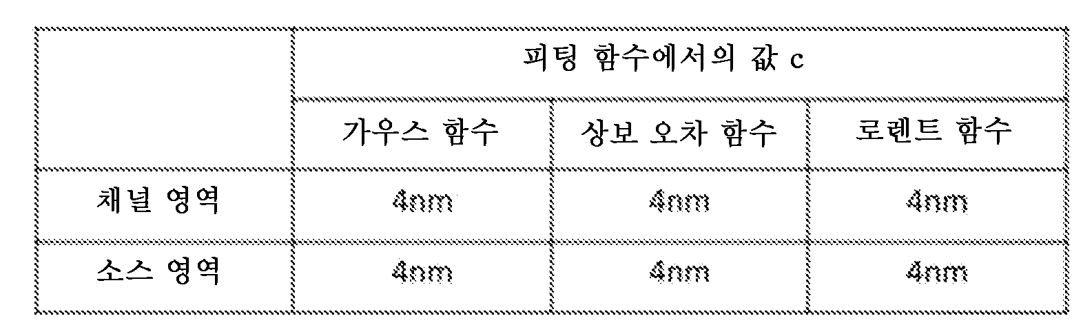
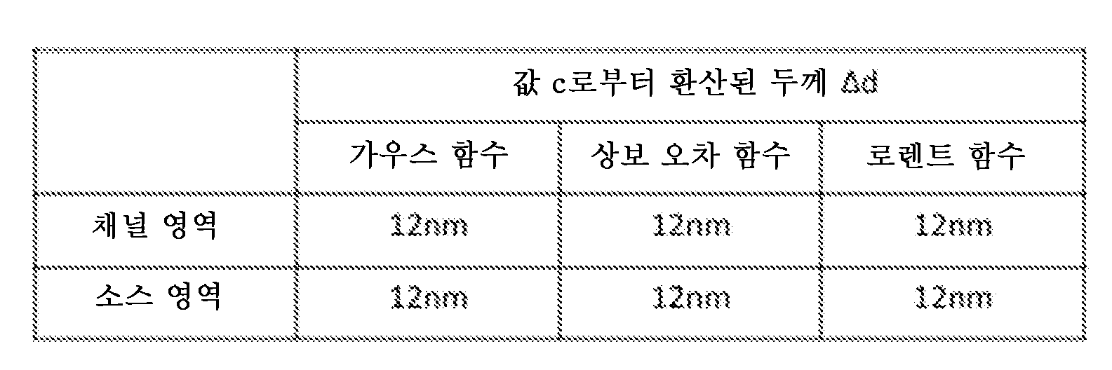
표 2에 나타낸 바와 같이, 어느 피팅 함수를 사용하여도, 실시예 A의 산화물 반도체층(140)에 있어서의 Al의 농도 구배를 갖는 영역의 두께 Δd는, 12㎚였다. 제1 실시 형태에 있어서 설명한 바와 같이, Al의 농도 구배를 갖는 영역의 두께 Δd의 전부가, 절연체와 같이 작용하는 것은 아니다. 여기에서는, c=4㎚에 대응하는 두께의 영역이, 절연체와 같이 작용하는 영역이 된다. 즉, 금속 산화물층(130)과 산화물 반도체층(140)과의 계면으로부터 4㎚까지의 두께의 영역이, 영역(140a)에 대응한다는 것을 알 수 있다. 다시 말해, 금속 산화물층(130)과 산화물 반도체층(140)과의 계면으로부터 5㎚ 이상의 영역은, 반도체로서 작용하는 영역이다.As shown in Table 2, the thickness Δd of the region having the Al concentration gradient in the oxide semiconductor layer (140) of Example A was 12 nm, regardless of which fitting function was used. As described in the first embodiment, not all of the thickness Δd of the region having the Al concentration gradient acts like an insulator. Here, the region having a thickness corresponding to c = 4 nm becomes a region acting like an insulator. That is, it can be seen that the region having a thickness of up to 4 nm from the interface between the metal oxide layer (130) and the oxide semiconductor layer (140) corresponds to the region (140a). In other words, the region 5 nm or more from the interface between the metal oxide layer (130) and the oxide semiconductor layer (140) is a region acting as a semiconductor.
도 26은, 실시예 A에 있어서의 박막 트랜지스터의 채널 영역에 있어서의 In의 EDX 분석 결과이다. 도 27은, 실시예 A에 있어서의 박막 트랜지스터의 소스 영역 근방에 있어서의 In의 EDX 분석 결과이다. 도 26 및 도 27에 있어서, 실시예 A에 있어서의 산화알루미늄층과 산화물 반도체층과의 계면은, 깊이(Depth)가 80㎚ 근방이다. 산화알루미늄층과 산화물 반도체층과의 계면을 점선으로 나타내고 있다. 또한, 80㎚를 기준으로 하여, 산화알루미늄층의 막 두께와, 산화물 반도체층의 막 두께를 점선으로 나타내고 있다.Fig. 26 shows the results of EDX analysis of In in the channel region of the thin film transistor in Example A. Fig. 27 shows the results of EDX analysis of In in the vicinity of the source region of the thin film transistor in Example A. In Figs. 26 and 27, the interface between the aluminum oxide layer and the oxide semiconductor layer in Example A has a depth of about 80 nm. The interface between the aluminum oxide layer and the oxide semiconductor layer is indicated by a dotted line. In addition, the film thickness of the aluminum oxide layer and the film thickness of the oxide semiconductor layer are indicated by dotted lines with 80 nm as a standard.
도 26 및 도 27에 도시한 바와 같이, 실시예 A에 있어서의 박막 트랜지스터에 있어서, 금속 산화물층(130)에는, 산화물 반도체층(140)에 포함되는 In이 포함된다는 것을 알 수 있다. 금속 산화물층(130)에 포함되는 In은 농도 구배를 갖고, In의 농도 구배는, 금속 산화물층(130)과 산화물 반도체층(140)과의 계면에 가까워짐에 따라서 증가한다는 것을 알 수 있다.As shown in FIG. 26 and FIG. 27, in the thin film transistor of Example A, it can be seen that the metal oxide layer (130) includes In included in the oxide semiconductor layer (140). It can be seen that the In included in the metal oxide layer (130) has a concentration gradient, and that the concentration gradient of In increases as it approaches the interface between the metal oxide layer (130) and the oxide semiconductor layer (140).
이상 설명한 바와 같이, 본 발명의 일 실시 형태에 있어서의 박막 트랜지스터에서는, 산화물 반도체층은, 금속 산화물층에 포함되는 금속 원소와 동일한 금속 원소가 농도 구배를 갖는 영역을 갖고, 금속 원소의 농도 구배는 금속 산화물층과 산화물 반도체층과의 계면에 가까워짐에 따라서 증가한다는 특징을 갖는다. 이에 의해, 산화물 반도체층을 양호하게 결정화함과 함께, 채널로서 기능하는 두께를 실질적으로 작게 할 수 있다는 것이 시사되었다. 이에 의해, 채널로서 기능하는 영역에 있어서, 캐리어 농도를 높일 수 있다. 그 때문에, 박막 트랜지스터의 전계 효과의 이동도를 대폭으로 증가시킬 수 있다고 생각된다.As described above, in the thin film transistor according to one embodiment of the present invention, the oxide semiconductor layer has a region in which the same metal element as the metal element included in the metal oxide layer has a concentration gradient, and the concentration gradient of the metal element increases as it approaches the interface between the metal oxide layer and the oxide semiconductor layer. This suggests that the oxide semiconductor layer can be well crystallized and the thickness functioning as a channel can be substantially reduced. This makes it possible to increase the carrier concentration in the region functioning as a channel. Therefore, it is thought that the field effect mobility of the thin film transistor can be significantly increased.
본 발명의 실시 형태로서 상술한 각 실시 형태는, 서로 모순되지 않는 한, 적절히 조합하여 실시할 수 있다. 또한, 각 실시 형태를 기초로 하여, 당업자가 적절히 구성 요소의 추가, 삭제, 혹은 설계 변경을 행한 것, 또는 공정의 추가, 생략 혹은 조건 변경을 행한 것도, 본 발명의 요지를 구비하고 있는 한, 본 발명의 범위에 포함된다.The embodiments described above as embodiments of the present invention can be appropriately combined and implemented as long as they are not contradictory to each other. In addition, based on each embodiment, those skilled in the art may appropriately add, delete, or change the design of components, or add, omit, or change conditions of processes, as long as they retain the gist of the present invention. These are also included in the scope of the present invention.
상술한 각 실시 형태의 양태에 의해 초래되는 작용 효과와는 상이한 다른 작용 효과라도, 본 명세서의 기재로부터 명확한 것, 또는 당업자에 있어서 용이하게 예측할 수 있는 것에 대해서는, 당연히 본 발명에 의해 초래되는 것이라고 해석된다.Even if there are other effects that are different from the effects brought about by the aspects of each embodiment described above, those that are clear from the description of this specification or can be easily predicted by a person skilled in the art are naturally interpreted as being brought about by the present invention.
1: 적층 구조체
10: 박막 트랜지스터
11: 하지 절연층
100: 기판
105, 160: 게이트 전극
110, 120, 150: 게이트 절연층
130: 금속 산화물층
140: 산화물 반도체층
140a: 영역
140b: 영역
141: 상면
142: 하면
143: 측면
170, 180: 절연층
171, 173: 개구
200: 소스·드레인 전극
201: 소스 전극
203: 드레인 전극
1000: 전자 기기
1100: 표시 장치1: Laminated structure
10: Thin film transistor
11: No insulation layer
100: Substrate
105, 160: Gate electrode
110, 120, 150: Gate insulation layer
130: Metal oxide layer
140: Oxide semiconductor layer
140a: Area
140b: Area
141: Top surface
142: If you do
143: Side
170, 180: Insulation layer
171, 173: Opening
200: Source/drain electrodes
201: Source electrode
203: Drain electrode
1000: Electronic Devices
1100: Display Device
Claims (10)
상기 하지 절연층 위에 마련된 금속 산화물층과,
상기 금속 산화물층에 접해서 마련된, 다결정 구조를 갖는 산화물 반도체층
을 갖고,
상기 산화물 반도체층은, 상기 금속 산화물층에 포함되는 금속 원소와 동일한 금속 원소가 농도 구배를 갖는 제1 영역을 갖고, 상기 금속 원소의 농도 구배는 상기 금속 산화물층과 상기 산화물 반도체층과의 계면에 가까워짐에 따라서 증가하는, 적층 구조체.And the insulating layer,
A metal oxide layer provided on the above insulating layer,
An oxide semiconductor layer having a polycrystalline structure, which is formed in contact with the above metal oxide layer
Have,
A laminated structure in which the oxide semiconductor layer has a first region in which a metal element identical to a metal element included in the metal oxide layer has a concentration gradient, and the concentration gradient of the metal element increases as it approaches an interface between the metal oxide layer and the oxide semiconductor layer.
상기 산화물 반도체층은, 적어도 15㎚ 이상의 두께를 갖고,
상기 제1 영역은, 상기 산화물 반도체층의 두께 방향에 있어서, 상기 금속 산화물층과의 계면으로부터 14㎚ 미만의 영역인, 적층 구조체.In the first paragraph,
The above oxide semiconductor layer has a thickness of at least 15 nm,
A laminated structure in which the first region is a region less than 14 nm from the interface with the metal oxide layer in the thickness direction of the oxide semiconductor layer.
상기 산화물 반도체층은, 적어도 15㎚ 이상의 두께를 갖고,
상기 산화물 반도체층은, 상기 금속 산화물층과 접하지 않는 측에, 상기 금속 원소의 농도 구배를 갖지 않는 제2 영역을 더 갖고,
상기 제2 영역은, 상기 제1 영역과 접함과 함께, 상기 산화물 반도체층의 두께 방향에 있어서, 1㎚ 이상의 두께를 갖는, 적층 구조체.In the first paragraph,
The above oxide semiconductor layer has a thickness of at least 15 nm,
The above oxide semiconductor layer further has a second region that does not have a concentration gradient of the metal element on a side that does not come into contact with the metal oxide layer,
A laminated structure in which the second region, together with the first region, has a thickness of 1 nm or more in the thickness direction of the oxide semiconductor layer.
상기 산화물 반도체층은, 인듐과,
상기 인듐 원소를 제외한 적어도 하나 이상의 금속 원소를 포함하고,
상기 금속 산화물층은, 상기 인듐이 포함되는 영역을 갖는, 적층 구조체.In the first paragraph,
The above oxide semiconductor layer comprises indium and
Containing at least one metal element other than the above indium element,
The above metal oxide layer is a laminated structure having a region containing the indium.
상기 산화물 반도체층은, 상기 인듐 및 상기 적어도 하나 이상의 금속 원소에 대한 상기 인듐의 비율은 50% 이상인 영역을 포함하는, 적층 구조체.In paragraph 4,
A laminated structure, wherein the oxide semiconductor layer includes a region in which the ratio of indium to the indium and the at least one metal element is 50% or more.
상기 금속 산화물층에 포함되는 상기 인듐 원소는 농도 구배를 갖고, 상기 인듐 원소의 농도 구배는, 상기 금속 산화물층과 상기 산화물 반도체층과의 계면에 가까워짐에 따라서 증가하는, 적층 구조체.In paragraph 5,
A laminated structure in which the indium element included in the metal oxide layer has a concentration gradient, and the concentration gradient of the indium element increases as it approaches the interface between the metal oxide layer and the oxide semiconductor layer.
상기 금속 산화물층은, 밴드 갭이 4.0eV 이상의 금속 산화물을 포함하는, 적층 구조체.In the first paragraph,
The above metal oxide layer is a laminated structure including a metal oxide having a band gap of 4.0 eV or more.
상기 금속 산화물층은, 상기 금속 원소로서 알루미늄(Al), 마그네슘(Mg), 칼슘(Ca), 스칸듐(Sc), 갈륨(Ga), 게르마늄(Ge), 스트론튬(Sr), 니켈(Ni), 탄탈(Ta), 이트륨(Y), 지르코늄(Zr), 바륨(Ba), 하프늄(Hf), 코발트(Co) 및 란타노이드계 원소로부터 선택된 1개 또는 복수의 금속 원소를 포함하는, 적층 구조체.In the first paragraph,
A laminated structure in which the metal oxide layer comprises one or more metal elements selected from aluminum (Al), magnesium (Mg), calcium (Ca), scandium (Sc), gallium (Ga), germanium (Ge), strontium (Sr), nickel (Ni), tantalum (Ta), yttrium (Y), zirconium (Zr), barium (Ba), hafnium (Hf), cobalt (Co), and lanthanoid elements as the metal elements.
상기 산화물 반도체층은, 빅스바이트형의 결정 구조를 갖는 것을 특징으로 하는, 적층 구조체.In the first paragraph,
A laminated structure, characterized in that the above oxide semiconductor layer has a bixbyite type crystal structure.
상기 산화물 반도체층 위에 마련된 게이트 절연막과,
상기 게이트 절연막 위에, 상기 산화물 반도체층의 적어도 일부와 중첩하도록 마련된 게이트 전극을 갖는 박막 트랜지스터.The laminated structure described in Article 1,
A gate insulating film provided on the above oxide semiconductor layer,
A thin film transistor having a gate electrode arranged to overlap at least a portion of the oxide semiconductor layer on the gate insulating film.
Applications Claiming Priority (3)
| Application Number | Priority Date | Filing Date | Title |
|---|---|---|---|
| JP2022122911 | 2022-08-01 | ||
| JPJP-P-2022-122911 | 2022-08-01 | ||
| PCT/JP2023/027457 WO2024029429A1 (en) | 2022-08-01 | 2023-07-26 | Laminate structure and thin-film transistor |
Publications (1)
| Publication Number | Publication Date |
|---|---|
| KR20250026275A true KR20250026275A (en) | 2025-02-25 |
Family
ID=89848999
Family Applications (1)
| Application Number | Title | Priority Date | Filing Date |
|---|---|---|---|
| KR1020257001779A Pending KR20250026275A (en) | 2022-08-01 | 2023-07-26 | Laminated structures and thin film transistors |
Country Status (7)
| Country | Link |
|---|---|
| US (1) | US20250176220A1 (en) |
| JP (1) | JPWO2024029429A1 (en) |
| KR (1) | KR20250026275A (en) |
| CN (1) | CN119604968A (en) |
| DE (1) | DE112023002495T5 (en) |
| TW (1) | TWI858841B (en) |
| WO (1) | WO2024029429A1 (en) |
Citations (6)
| Publication number | Priority date | Publication date | Assignee | Title |
|---|---|---|---|---|
| JP2014099601A (en) | 2012-10-19 | 2014-05-29 | Semiconductor Energy Lab Co Ltd | Multilayer film including oxide semiconductor film and manufacturing method for semiconductor device |
| JP2016184771A (en) | 2012-08-03 | 2016-10-20 | 株式会社半導体エネルギー研究所 | Semiconductor device |
| JP2018006730A (en) | 2016-02-12 | 2018-01-11 | 株式会社半導体エネルギー研究所 | Semiconductor device and display device having semiconductor device |
| JP2021108405A (en) | 2010-09-13 | 2021-07-29 | 株式会社半導体エネルギー研究所 | Manufacturing method of semiconductor device |
| JP2021141338A (en) | 2012-09-14 | 2021-09-16 | 株式会社半導体エネルギー研究所 | Manufacturing method for semiconductor device |
| JP2021153196A (en) | 2013-09-23 | 2021-09-30 | 株式会社半導体エネルギー研究所 | Semiconductor device |
Family Cites Families (6)
| Publication number | Priority date | Publication date | Assignee | Title |
|---|---|---|---|---|
| KR20130032304A (en) * | 2010-04-02 | 2013-04-01 | 가부시키가이샤 한도오따이 에네루기 켄큐쇼 | Semiconductor device |
| JP6231880B2 (en) * | 2011-08-11 | 2017-11-15 | 出光興産株式会社 | Thin film transistor |
| TWI567985B (en) * | 2011-10-21 | 2017-01-21 | 半導體能源研究所股份有限公司 | Semiconductor device and method of manufacturing same |
| CN105027296B (en) * | 2013-03-07 | 2018-11-06 | 夏普株式会社 | Semiconductor device and its manufacturing method |
| JP6692645B2 (en) * | 2016-01-15 | 2020-05-13 | 株式会社ジャパンディスプレイ | Semiconductor device |
| US10845704B2 (en) * | 2018-10-30 | 2020-11-24 | Taiwan Semiconductor Manufacturing Co., Ltd. | Extreme ultraviolet photolithography method with infiltration for enhanced sensitivity and etch resistance |
-
2023
- 2023-07-26 KR KR1020257001779A patent/KR20250026275A/en active Pending
- 2023-07-26 DE DE112023002495.2T patent/DE112023002495T5/en active Pending
- 2023-07-26 CN CN202380055153.3A patent/CN119604968A/en active Pending
- 2023-07-26 WO PCT/JP2023/027457 patent/WO2024029429A1/en not_active Ceased
- 2023-07-26 JP JP2024539107A patent/JPWO2024029429A1/ja active Pending
- 2023-08-01 TW TW112128779A patent/TWI858841B/en active
-
2025
- 2025-01-28 US US19/039,202 patent/US20250176220A1/en active Pending
Patent Citations (6)
| Publication number | Priority date | Publication date | Assignee | Title |
|---|---|---|---|---|
| JP2021108405A (en) | 2010-09-13 | 2021-07-29 | 株式会社半導体エネルギー研究所 | Manufacturing method of semiconductor device |
| JP2016184771A (en) | 2012-08-03 | 2016-10-20 | 株式会社半導体エネルギー研究所 | Semiconductor device |
| JP2021141338A (en) | 2012-09-14 | 2021-09-16 | 株式会社半導体エネルギー研究所 | Manufacturing method for semiconductor device |
| JP2014099601A (en) | 2012-10-19 | 2014-05-29 | Semiconductor Energy Lab Co Ltd | Multilayer film including oxide semiconductor film and manufacturing method for semiconductor device |
| JP2021153196A (en) | 2013-09-23 | 2021-09-30 | 株式会社半導体エネルギー研究所 | Semiconductor device |
| JP2018006730A (en) | 2016-02-12 | 2018-01-11 | 株式会社半導体エネルギー研究所 | Semiconductor device and display device having semiconductor device |
Also Published As
| Publication number | Publication date |
|---|---|
| CN119604968A (en) | 2025-03-11 |
| DE112023002495T5 (en) | 2025-04-10 |
| WO2024029429A1 (en) | 2024-02-08 |
| JPWO2024029429A1 (en) | 2024-02-08 |
| TW202408020A (en) | 2024-02-16 |
| US20250176220A1 (en) | 2025-05-29 |
| TWI858841B (en) | 2024-10-11 |
Similar Documents
| Publication | Publication Date | Title |
|---|---|---|
| US20250176237A1 (en) | Oxide semiconductor film, thin film transistor, and electronic device | |
| KR20250026275A (en) | Laminated structures and thin film transistors | |
| TWI887624B (en) | Thin film transistors and electronic devices | |
| TWI854563B (en) | Oxide semiconductor film, thin film transistor, and electronic device | |
| TWI876308B (en) | Thin film transistors and electronic devices | |
| US20250176222A1 (en) | Oxide semiconductor film, thin film transistor, and electronic device | |
| KR102733354B1 (en) | Method of manufacturing semiconductor device | |
| US20240113228A1 (en) | Semiconductor device and method for manufacturing semiconductor device | |
| KR102843075B1 (en) | Semiconductor device | |
| US20250380465A1 (en) | Semiconductor device and manufacturing method thereof | |
| US20260006828A1 (en) | Semiconductor device and manufacturing method thereof | |
| KR102874155B1 (en) | Method for manufacturing semiconductor device | |
| US20250113543A1 (en) | Semiconductor device | |
| US20250113542A1 (en) | Semiconductor device | |
| KR20240169711A (en) | semiconductor devices | |
| CN118891736A (en) | Semiconductor device with a semiconductor device having a plurality of semiconductor chips | |
| TW202439467A (en) | Oxide semiconductor film, multilayer structure, thin film transistor, and electronic device | |
| KR20240147486A (en) | Semiconductor device and manufacturing method of semiconductor device | |
| CN118872072A (en) | Semiconductor devices | |
| KR20250047879A (en) | Semiconductor device | |
| WO2023189489A1 (en) | Semiconductor device | |
| KR20250117810A (en) | Thin film transistors and electronic devices | |
| CN118872073A (en) | Semiconductor devices | |
| KR20230141498A (en) | Manufacturing method of semiconductor device | |
| CN120659359A (en) | semiconductor devices |
Legal Events
| Date | Code | Title | Description |
|---|---|---|---|
| PA0105 | International application |
St.27 status event code: A-0-1-A10-A15-nap-PA0105 |
|
| PA0201 | Request for examination |
St.27 status event code: A-1-2-D10-D11-exm-PA0201 |
|
| PG1501 | Laying open of application |
St.27 status event code: A-1-1-Q10-Q12-nap-PG1501 |
|
| D21 | Rejection of application intended |
Free format text: ST27 STATUS EVENT CODE: A-1-2-D10-D21-EXM-PE0902 (AS PROVIDED BY THE NATIONAL OFFICE) |
|
| PE0902 | Notice of grounds for rejection |
St.27 status event code: A-1-2-D10-D21-exm-PE0902 |
|
| T11 | Administrative time limit extension requested |
Free format text: ST27 STATUS EVENT CODE: U-3-3-T10-T11-OTH-X000 (AS PROVIDED BY THE NATIONAL OFFICE) |
|
| T11-X000 | Administrative time limit extension requested |
St.27 status event code: U-3-3-T10-T11-oth-X000 |
|
| P11 | Amendment of application requested |
Free format text: ST27 STATUS EVENT CODE: A-2-2-P10-P11-NAP-X000 (AS PROVIDED BY THE NATIONAL OFFICE) |
|
| P11-X000 | Amendment of application requested |
St.27 status event code: A-2-2-P10-P11-nap-X000 |