KR20240150465A - Display device - Google Patents
Display device Download PDFInfo
- Publication number
- KR20240150465A KR20240150465A KR1020247030108A KR20247030108A KR20240150465A KR 20240150465 A KR20240150465 A KR 20240150465A KR 1020247030108 A KR1020247030108 A KR 1020247030108A KR 20247030108 A KR20247030108 A KR 20247030108A KR 20240150465 A KR20240150465 A KR 20240150465A
- Authority
- KR
- South Korea
- Prior art keywords
- assembly
- electrode
- extension
- sub
- wiring
- Prior art date
- Legal status (The legal status is an assumption and is not a legal conclusion. Google has not performed a legal analysis and makes no representation as to the accuracy of the status listed.)
- Pending
Links
Images


Classifications
-
- H—ELECTRICITY
- H10—SEMICONDUCTOR DEVICES; ELECTRIC SOLID-STATE DEVICES NOT OTHERWISE PROVIDED FOR
- H10H—INORGANIC LIGHT-EMITTING SEMICONDUCTOR DEVICES HAVING POTENTIAL BARRIERS
- H10H29/00—Integrated devices, or assemblies of multiple devices, comprising at least one light-emitting semiconductor element covered by group H10H20/00
- H10H29/01—Manufacture or treatment
- H10H29/03—Manufacture or treatment using mass transfer of LEDs, e.g. by using liquid suspensions
-
- H01L27/156—
-
- H—ELECTRICITY
- H10—SEMICONDUCTOR DEVICES; ELECTRIC SOLID-STATE DEVICES NOT OTHERWISE PROVIDED FOR
- H10H—INORGANIC LIGHT-EMITTING SEMICONDUCTOR DEVICES HAVING POTENTIAL BARRIERS
- H10H29/00—Integrated devices, or assemblies of multiple devices, comprising at least one light-emitting semiconductor element covered by group H10H20/00
- H10H29/30—Active-matrix LED displays
- H10H29/49—Interconnections, e.g. wiring lines or terminals
-
- H—ELECTRICITY
- H10—SEMICONDUCTOR DEVICES; ELECTRIC SOLID-STATE DEVICES NOT OTHERWISE PROVIDED FOR
- H10H—INORGANIC LIGHT-EMITTING SEMICONDUCTOR DEVICES HAVING POTENTIAL BARRIERS
- H10H29/00—Integrated devices, or assemblies of multiple devices, comprising at least one light-emitting semiconductor element covered by group H10H20/00
- H10H29/10—Integrated devices comprising at least one light-emitting semiconductor component covered by group H10H20/00
- H10H29/14—Integrated devices comprising at least one light-emitting semiconductor component covered by group H10H20/00 comprising multiple light-emitting semiconductor components
- H10H29/142—Two-dimensional arrangements, e.g. asymmetric LED layout
-
- H—ELECTRICITY
- H01—ELECTRIC ELEMENTS
- H01L—SEMICONDUCTOR DEVICES NOT COVERED BY CLASS H10
- H01L25/00—Assemblies consisting of a plurality of semiconductor or other solid state devices
- H01L25/16—Assemblies consisting of a plurality of semiconductor or other solid state devices the devices being of types provided for in two or more different subclasses of H10B, H10D, H10F, H10H, H10K or H10N, e.g. forming hybrid circuits
- H01L25/167—Assemblies consisting of a plurality of semiconductor or other solid state devices the devices being of types provided for in two or more different subclasses of H10B, H10D, H10F, H10H, H10K or H10N, e.g. forming hybrid circuits comprising optoelectronic devices, e.g. LED, photodiodes
-
- H01L33/38—
-
- H01L33/483—
-
- H01L33/62—
-
- H—ELECTRICITY
- H10—SEMICONDUCTOR DEVICES; ELECTRIC SOLID-STATE DEVICES NOT OTHERWISE PROVIDED FOR
- H10H—INORGANIC LIGHT-EMITTING SEMICONDUCTOR DEVICES HAVING POTENTIAL BARRIERS
- H10H20/00—Individual inorganic light-emitting semiconductor devices having potential barriers, e.g. light-emitting diodes [LED]
- H10H20/80—Constructional details
- H10H20/83—Electrodes
- H10H20/831—Electrodes characterised by their shape
-
- H—ELECTRICITY
- H10—SEMICONDUCTOR DEVICES; ELECTRIC SOLID-STATE DEVICES NOT OTHERWISE PROVIDED FOR
- H10H—INORGANIC LIGHT-EMITTING SEMICONDUCTOR DEVICES HAVING POTENTIAL BARRIERS
- H10H20/00—Individual inorganic light-emitting semiconductor devices having potential barriers, e.g. light-emitting diodes [LED]
- H10H20/80—Constructional details
- H10H20/85—Packages
- H10H20/8506—Containers
-
- H—ELECTRICITY
- H10—SEMICONDUCTOR DEVICES; ELECTRIC SOLID-STATE DEVICES NOT OTHERWISE PROVIDED FOR
- H10H—INORGANIC LIGHT-EMITTING SEMICONDUCTOR DEVICES HAVING POTENTIAL BARRIERS
- H10H20/00—Individual inorganic light-emitting semiconductor devices having potential barriers, e.g. light-emitting diodes [LED]
- H10H20/80—Constructional details
- H10H20/85—Packages
- H10H20/857—Interconnections, e.g. lead-frames, bond wires or solder balls
-
- H—ELECTRICITY
- H10—SEMICONDUCTOR DEVICES; ELECTRIC SOLID-STATE DEVICES NOT OTHERWISE PROVIDED FOR
- H10H—INORGANIC LIGHT-EMITTING SEMICONDUCTOR DEVICES HAVING POTENTIAL BARRIERS
- H10H29/00—Integrated devices, or assemblies of multiple devices, comprising at least one light-emitting semiconductor element covered by group H10H20/00
- H10H29/30—Active-matrix LED displays
- H10H29/32—Active-matrix LED displays characterised by the geometry or arrangement of elements within a subpixel, e.g. arrangement of the transistor within its RGB subpixel
-
- H10W90/00—
Landscapes
- Devices For Indicating Variable Information By Combining Individual Elements (AREA)
- Electroluminescent Light Sources (AREA)
- Engineering & Computer Science (AREA)
- Microelectronics & Electronic Packaging (AREA)
- Physics & Mathematics (AREA)
- Condensed Matter Physics & Semiconductors (AREA)
- General Physics & Mathematics (AREA)
- Computer Hardware Design (AREA)
- Power Engineering (AREA)
Abstract
디스플레이 장치는 복수의 서브 화소를 포함하는 기판과, 복수의 서브 화소 각각에 제1 조립 배선과, 복수의 서브 화소 각각에 제2 조립 배선과, 제1 조립 배선 및 제2 조립 배선 상에 조립 홀을 갖는 격벽과, 조립 홀에 반도체 발광 소자를 포함한다.
제1 조립 배선은 제1 버스 라인과, 제1 버스 라인 상에 제1 조립 전극을 포함할 수 있다. 제1 버스 라인의 일부는 조립 홀에 인접하여 배치되고, 제1 조립 전극의 일부는 조립 홀에 배치될 수 있다.A display device includes a substrate including a plurality of sub-pixels, a first assembly wiring for each of the plurality of sub-pixels, a second assembly wiring for each of the plurality of sub-pixels, a partition wall having an assembly hole on the first assembly wiring and the second assembly wiring, and a semiconductor light-emitting element in the assembly hole.
The first assembly wiring may include a first bus line and a first assembly electrode on the first bus line. A portion of the first bus line may be positioned adjacent to the assembly hole, and a portion of the first assembly electrode may be positioned in the assembly hole.
Description
실시예는 디스플레이 장치에 관한 것이다.The embodiment relates to a display device.
대면적 디스플레이는 액정디스플레이(LCD), OLED 디스플레이, 그리고 마이크로-LED 디스플레이(Micro-LED display) 등이 있다.Large-area displays include liquid crystal displays (LCDs), OLED displays, and micro-LED displays.
마이크로-LED 디스플레이는 100㎛ 이하의 직경 또는 단면적을 가지는 반도체 발광 소자인 마이크로-LED를 표시소자로 사용하는 디스플레이이다.A micro-LED display is a display that uses micro-LEDs, which are semiconductor light-emitting elements with a diameter or cross-sectional area of 100㎛ or less, as display elements.
마이크로-LED 디스플레이는 반도체 발광 소자인 마이크로-LED를 표시소자로 사용하기 때문에 명암비, 응답속도, 색 재현율, 시야각, 밝기, 해상도, 수명, 발광효율이나 휘도 등 많은 특성에서 우수한 성능을 가지고 있다.Micro-LED displays use semiconductor light-emitting elements, such as micro-LEDs, as display elements, and therefore have superior performance in many characteristics, including contrast ratio, response speed, color reproducibility, viewing angle, brightness, resolution, lifespan, luminous efficacy, and brightness.
특히 마이크로-LED 디스플레이는 화면을 모듈 방식으로 분리, 결합할 수 있어 크기나 해상도 조절이 자유로운 장점 및 플렉서블 디스플레이 구현이 가능한 장점이 있다.In particular, micro-LED displays have the advantage of being able to freely adjust the size and resolution by separating and combining the screen in a modular manner, and of being able to implement a flexible display.
그런데 대형 마이크로-LED 디스플레이는 수백만 개 이상의 마이크로-LED가 필요로 하기 때문에 마이크로-LED를 디스플레이 패널에 신속하고 정확하게 전사하기 어려운 기술적 문제가 있다.However, since large-scale micro-LED displays require millions or more micro-LEDs, there is a technical challenge in quickly and accurately transferring micro-LEDs to the display panel.
최근 개발되고 있는 전사기술에는 픽앤-플레이스 공법(pick and place process), 레이저 리프트 오프법(Laser Lift-off method) 또는 자가조립 방식(self-assembly method) 등이 있다.Recently developed transcription technologies include the pick and place process, the laser lift-off method, and the self-assembly method.
이 중에서, 자가조립 방식은 유체 내에서 반도체 발광 소자가 조립위치를 스스로 찾아가는 방식으로서 대화면의 디스플레이 장치의 구현에 유리한 방식이다.Among these, the self-assembly method is advantageous for implementing large-screen display devices, as it is a method in which semiconductor light-emitting elements find their own assembly positions within a fluid.
하지만, 아직 마이크로-LED의 자가조립을 통하여 디스플레이를 제조하는 기술에 대한 연구가 미비한 실정이다.However, research on the technology for manufacturing displays through self-assembly of micro-LEDs is still insufficient.
특히 종래기술에서 대형 디스플레이에 수백만 개 이상의 반도체 발광 소자를 신속하게 전사하는 경우 전사 속도(transfer speed)는 향상시킬 수 있으나 전사 불량률(transfer error rate)이 높아질 수 있어 전사 수율(transfer yield)이 낮아지는 기술적 문제가 있다.In particular, in the case of rapidly transferring millions or more semiconductor light-emitting elements to a large display in the prior art, there is a technical problem that although the transfer speed can be improved, the transfer error rate can increase, resulting in a lower transfer yield.
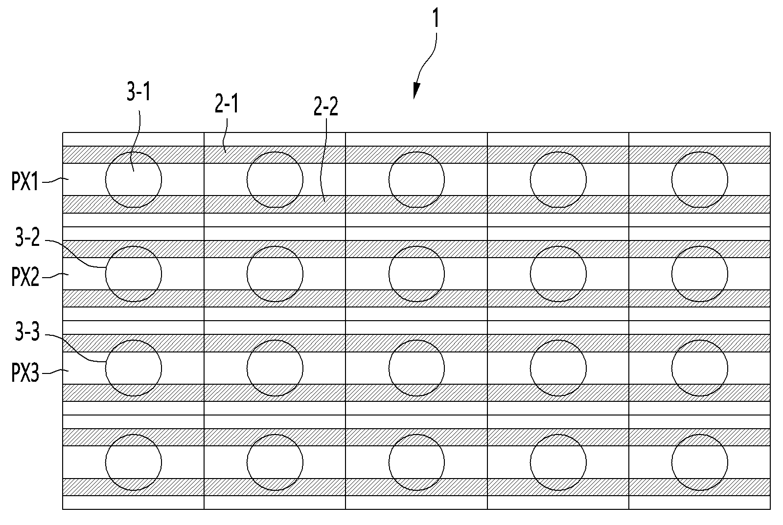
도 1은 제1 비공개 내부 기술에 따른 조립 기판을 도시한 평면도이다.Figure 1 is a plan view illustrating an assembled board according to the first non-public internal technology.
도 1에 도시한 바와 같이, 제1 비공개 내부 기술에 따른 조립 기판(1)은 복수의 서브 화소(PX1, PX2, PX3)를 포함할 수 있다. 복수의 서브 화소 서브 화소(PX1, PX2, PX3)에는 제1 조립 배선(2-1) 및 제1 조립 배선(2-2)이 구비된다.As illustrated in Fig. 1, an assembly substrate (1) according to the first non-public internal technology may include a plurality of sub-pixels (PX1, PX2, PX3). The plurality of sub-pixels (PX1, PX2, PX3) are provided with a first assembly wiring (2-1) and a first assembly wiring (2-2).
제1 조립 배선(2-1)과 제1 조립 배선(2-2) 사이에 형성된 유전영동힘(DEP force)에 의해 복수의 반도체 발광 소자(3-1, 3-2, 3-3)이 각각 복수의 서브 화소(PX1, PX2, PX3)에 조립된다.A plurality of semiconductor light-emitting elements (3-1, 3-2, 3-3) are assembled into a plurality of sub-pixels (PX1, PX2, PX3) respectively by the dielectric electrophoretic force (DEP force) formed between the first assembly wiring (2-1) and the first assembly wiring (2-2).
DEP force는 제1 조립 배선(2-1)과 제2 조립 배선(2-2)에 공급된 교류 전압(도 2의 V(+)1, V(-)1)에 형성된다.The DEP force is formed by the AC voltage (V(+)1, V(-)1 in Fig. 2) supplied to the first assembly wiring (2-1) and the second assembly wiring (2-2).
제1 조립 배선(2-1)과 제2 조립 배선(2-2) 각각의 두께가 얇거나 길이가 길수록 선 저항이 커진다.The thinner or longer the first assembly wiring (2-1) and the second assembly wiring (2-2), the greater the wire resistance.
도 1에 도시한 바와 같이, 해상도가 낮은 경우 제1 조립 배선(2-1) 및 제1 조립 배선(2-2) 각각의 폭이 커, 선 저항이 높지 않아 제1 조립 배선(2-1) 및 제1 조립 배선(2-2) 각각의 길이 방향을 따라 교류 전압(V(+)1, V(-)1)의 전압 강하나 신호 지연이 발생되지 않는다. 이에 따라, 각 서브 화소(PX1, PX2, PX3)의 제1 조립 배선(2-1) 및 제1 조립 배선(2-2) 사이에 형성된 DEP force가 목표치와 일치하므로 복수의 반도체 발광 소자(3-1, 3-2, 3-3)이 각각 서브 화소(PX1, PX2, PX3)에 잘 조립되므로, 조립율 저하 문제가 발생하지 않는다.As illustrated in FIG. 1, when the resolution is low, the width of each of the first assembly wiring (2-1) and the first assembly wiring (2-2) is large, so that the line resistance is not high, and thus no voltage drop or signal delay of the AC voltage (V(+)1, V(-)1) occurs along the length direction of each of the first assembly wiring (2-1) and the first assembly wiring (2-2). Accordingly, since the DEP force formed between the first assembly wiring (2-1) and the first assembly wiring (2-2) of each sub-pixel (PX1, PX2, PX3) matches the target value, a plurality of semiconductor light-emitting elements (3-1, 3-2, 3-3) are properly assembled into each of the sub-pixels (PX1, PX2, PX3), and thus the problem of reduced assembly rate does not occur.
최근에는 고해상도 및 고정세도뿐만 아니라 대면적이 요구되고 있다. 이러한 요구 조건을 만족하기 위해, 조립 기판에 보다 많은 층과 보다 많은 회로가 구비되고 제한된 사이즈에 더 많은 화소(또는 서브 화소) 개수가 필요하다. 이에 따라, 각 화소의 사이즈가 작아짐에 따라 각 화소에 구비된 회로 선 폭이 작아지고 있다.Recently, not only high resolution and high definition but also large area are required. To meet these requirements, more layers and more circuits are equipped on the assembly board, and more pixels (or sub-pixels) are required in a limited size. Accordingly, as the size of each pixel decreases, the circuit line width equipped on each pixel is also decreasing.
즉, 도 3에 도시한 바와 같이, 제2 비공개 기술에 따른 조립 기판(5)의 복수의 서브 화소(PX1, PX2, PX3) 각각의 사이즈는 도 1에 도시된 조립 기판(1)의 복수의 서브 화소(PX1, PX2, PX3) 각각의 사이즈보다 작다. 이에 따라, 복수의 서브 화소(PX1, PX2, PX3) 각각에 구비된 제1 조립 배선(6-1) 및 제2 조립 배선(6-2) 각각의 선 폭 또한 작아진다. 이에 따라, 제1 조립 배선(6-1) 및 제2 조립 배선(6-2) 각각의 선 저항이 크게 증가된다.That is, as illustrated in FIG. 3, the size of each of the plurality of sub-pixels (PX1, PX2, PX3) of the assembly board (5) according to the second non-public technology is smaller than the size of each of the plurality of sub-pixels (PX1, PX2, PX3) of the assembly board (1) illustrated in FIG. 1. Accordingly, the line width of each of the first assembly wiring (6-1) and the second assembly wiring (6-2) provided in each of the plurality of sub-pixels (PX1, PX2, PX3) also becomes smaller. Accordingly, the line resistance of each of the first assembly wiring (6-1) and the second assembly wiring (6-2) significantly increases.
자가 조립시 DEP force를 형성하기 위해 제1 조립 배선(6-1) 및 제2 조립 배선(6-2)의 입력측에 교류 전압(도 2의 V(+)1, V(-)1)이 인가되는 경우, 제1 조립 배선(6-1) 및 제2 조립 배선(6-2) 각각의 커다란 선 저항으로 인해 해당 교류 전압(V(+)1, V(-)1)에 대한 전압 강하가 발생하여, 복수의 서브 화소(PX1, PX2, PX3) 각각에서 도 4에 도시한 바와 같이 신호 왜곡을 갖는 교류 전압(V(+)2, V(-)2)을 가진다. 즉, 교류 전압의 진폭이 A1(도 2)에서 A2(도 4)로 감소함에 따라, 복수의 서브 화소(PX1, PX2, PX3) 각각의 제1 조립 배선(6-1) 및 제2 조립 배선(6-2) 사이에 형성된 DEP force가 감소한다. 이에 따라, 복수의 서브 화소(PX1, PX2, PX3) 각각에서 복수의 반도체 발광 소자(8-1, 8-2, 8-3)를 고정시키는 고정력이 약해 조립 불량이 발생되어, 조립율이 저하되는 문제가 있다.When an AC voltage (V(+)1, V(-)1 in FIG. 2) is applied to the input sides of the first assembly wire (6-1) and the second assembly wire (6-2) to form a DEP force during self-assembly, a voltage drop occurs for the AC voltage (V(+)1, V(-)1) due to the large line resistance of each of the first assembly wire (6-1) and the second assembly wire (6-2), so that each of the plurality of sub-pixels (PX1, PX2, PX3) has an AC voltage (V(+)2, V(-)2) with signal distortion, as shown in FIG. 4. That is, as the amplitude of the AC voltage decreases from A1 (FIG. 2) to A2 (FIG. 4), the DEP force formed between the first assembly wire (6-1) and the second assembly wire (6-2) of each of the plurality of sub-pixels (PX1, PX2, PX3) decreases. Accordingly, there is a problem that the fixing force for fixing the plurality of semiconductor light-emitting elements (8-1, 8-2, 8-3) in each of the plurality of sub-pixels (PX1, PX2, PX3) is weak, resulting in assembly defects and a reduced assembly rate.
한편, 고해상도 및 고정세도뿐만 아니라 대면적의 요구 조건을 만족하기 위해, 조립 기판에 보다 많은 층과 보다 많은 회로가 구비됨에 따라 커패시턴스가 증가되고 있다. 이에 따라, 제1 조립 배선(6-1) 및 제2 조립 배선(6-2) 각각의 선 저항 증가와 더불어 커패시턴스가 증가함에 따라, 신호 지연(또는 RC 지연)에 의해 신호 왜곡이 발생한다. 그러므로, 교류 전압(V(+)2, V(-)2)의 진폭(A2)가 감소하여 조립율이 저하되는 문제가 있다.Meanwhile, in order to satisfy the requirements of high resolution and high definition as well as large area, the capacitance increases as more layers and more circuits are provided on the assembly board. Accordingly, as the line resistance of each of the first assembly wiring (6-1) and the second assembly wiring (6-2) increases and the capacitance increases, signal distortion occurs due to signal delay (or RC delay). Therefore, there is a problem that the amplitude (A2) of the AC voltage (V(+)2, V(-)2) decreases, resulting in a decrease in the assembly rate.
실시예는 전술한 문제 및 다른 문제를 해결하는 것을 목적으로 한다.The present invention aims to solve the above-mentioned and other problems.
실시예의 다른 목적은 새로운 구조를 갖는 디스플레이 장치를 제공하는 것이다.Another object of the invention is to provide a display device having a novel structure.
또한, 실시예의 또 다른 목적은 고해상도 및 고정세도를 갖는 디스플레이 장치를 제공하는 것이다.In addition, another object of the embodiment is to provide a display device having high resolution and high definition.
또한 실시예의 또 다른 목적은 대화면을 갖는 디스플레이 장치를 제공하는 것이다.Another object of the invention is to provide a display device having a large screen.
또한 실시예의 또 다른 목적은 조립율을 향상시킬 수 있는 디스플레이 장치를 제공하는 것이다.Another object of the embodiment is to provide a display device capable of improving assembly rate.
실시예의 기술적 과제는 본 항목에 기재된 것에 한정되지 않으며, 발명의 설명을 통해 파악될 수 있는 것을 포함한다.The technical problems of the embodiment are not limited to those described in this article, but include those that can be understood through the description of the invention.
상기 또는 다른 목적을 달성하기 위해 실시예의 일 측면에 따르면, 디스플레이 장치는, 복수의 서브 화소를 포함하는 기판; 상기 복수의 서브 화소 각각에 제1 조립 배선; 상기 복수의 서브 화소 각각에 제2 조립 배선; 상기 제1 조립 배선 및 상기 제2 조립 배선 상에 조립 홀을 갖는 격벽; 및 상기 조립 홀에 반도체 발광 소자;를 포함하고, 상기 제1 조립 배선은, 제1 버스 라인; 및 상기 제1 버스 라인 상에 제1 조립 전극;을 포함하고, 상기 제1 버스 라인의 일부는 상기 조립 홀에 인접하여 배치되고, 상기 제1 조립 전극의 일부는 상기 조립 홀에 배치될 수 있다.According to one aspect of the embodiment to achieve the above or other purposes, a display device includes a substrate including a plurality of sub-pixels; a first assembly wiring for each of the plurality of sub-pixels; a second assembly wiring for each of the plurality of sub-pixels; a partition wall having an assembly hole on the first assembly wiring and the second assembly wiring; and a semiconductor light-emitting element in the assembly hole; wherein the first assembly wiring includes a first bus line; and a first assembly electrode on the first bus line; a part of the first bus line may be disposed adjacent to the assembly hole, and a part of the first assembly electrode may be disposed in the assembly hole.
상기 제1 조립 배선은, 상기 제1 버스 라인으로부터 상기 조립 홀을 향해 연장되는 제1 연장 라인; 및 상기 제1 조립 전극으로부터 상기 조립 홀을 향해 연장되는 제1 연장 전극;을 포함할 수 있다. 상기 제1 연장 라인은 상기 조립 홀과 수직으로 중첩되지 않고, 상기 제1 연장 전극은 상기 조립 홀과 수직으로 중첩될 수 있다.The first assembly wiring may include a first extension line extending from the first bus line toward the assembly hole; and a first extension electrode extending from the first assembly electrode toward the assembly hole. The first extension line may not vertically overlap the assembly hole, and the first extension electrode may vertically overlap the assembly hole.
상기 제1 조립 전극의 폭은 상기 제1 버스 라인의 폭보다 크고, 제1 방향에 따른 상기 제1 연장 전극의 폭은 상기 제1 연장 라인의 폭보다 크고, 제2 방향에 따른 상기 제1 연장 전극의 폭은 상기 제1 연장 라인의 폭보다 작을 수 있다.The width of the first assembly electrode may be greater than the width of the first bus line, the width of the first extension electrode along the first direction may be greater than the width of the first extension line, and the width of the first extension electrode along the second direction may be smaller than the width of the first extension line.
상기 제2 조립 배선은, 제2 버스 라인; 및 상기 제2 버스 라인 상에 제2 조립 전극;을 포함하고, 상기 제2 버스 라인의 일부는 상기 조립 홀에 인접하여 배치되고, 상기 제2 조립 전극의 일부는 상기 조립 홀에 배치될 수 있다.The second assembly wiring includes a second bus line; and a second assembly electrode on the second bus line; a part of the second bus line may be arranged adjacent to the assembly hole, and a part of the second assembly electrode may be arranged in the assembly hole.
상기 제2 조립 배선은, 상기 제2 버스 라인으로부터 상기 조립 홀을 향해 연장되는 제2 연장 라인; 및 상기 제2 조립 전극으로부터 상기 조립 홀을 향해 연장되는 제2 연장 전극;을 포함할 수 있다. 상기 제2 연장 라인은 상기 조립 홀과 수직으로 중첩되지 않고, 상기 제2 연장 전극은 상기 조립 홀과 수직으로 중첩될 수 있다.The second assembly wiring may include a second extension line extending from the second bus line toward the assembly hole; and a second extension electrode extending from the second assembly electrode toward the assembly hole. The second extension line may not vertically overlap the assembly hole, and the second extension electrode may vertically overlap the assembly hole.
상기 제2 조립 전극의 폭은 상기 제2 버스 라인의 폭보다 크고, 제1 방향에 따른 상기 제2 연장 전극의 폭은 상기 제2 연장 라인의 폭보다 크고, 제2 방향에 따른 상기 제2 연장 전극의 폭은 상기 제2 연장 라인의 폭보다 작을 수 있다.The width of the second assembly electrode may be greater than the width of the second bus line, the width of the second extension electrode along the first direction may be greater than the width of the second extension line, and the width of the second extension electrode along the second direction may be smaller than the width of the second extension line.
상기 제1 연장 전극은 상기 제1 조립 전극으로부터 연장된 적어도 2개 이상의 전극을 포함할 수 있다. 상기 제2 연장 전극은 상기 제2 조립 전극으로부터 연장된 적어도 2개 이상의 전극을 포함할 수 있다.The first extension electrode may include at least two electrodes extending from the first assembly electrode. The second extension electrode may include at least two electrodes extending from the second assembly electrode.
상기 제1 연장 전극과 상기 제2 연장 전극은 서로 대칭적인 구조를 가질 수 있다. 상기 제1 연장 전극과 상기 제2 연장 전극은 서로 비대칭적인 구조를 가질 수 있다.The first extension electrode and the second extension electrode may have structures that are symmetrical to each other. The first extension electrode and the second extension electrode may have structures that are asymmetrical to each other.
상기 제1 버스 라인 및 상기 제2 버스 라인은 각각 상기 복수의 서브 화소를 가로질러 배치되고, 상기 제1 조립 전극은 상기 복수의 서브 화소 각각에서 상기 제1 버스 라인에 전기적으로 연결되고, 상기 제2 조립 전극은 상기 복수의 서브 화소 각각에서 상기 제2 버스 라인에 전기적으로 연결될 수 있다.The first bus line and the second bus line may be arranged across the plurality of sub-pixels, respectively, and the first assembly electrode may be electrically connected to the first bus line in each of the plurality of sub-pixels, and the second assembly electrode may be electrically connected to the second bus line in each of the plurality of sub-pixels.
상기 제1 조립 전극의 두께는 상기 제1 버스 라인의 두께보다 작고, 상기 제2 조립 전극의 두께는 상기 제2 버스 라인의 두께보다 작을 수 있다.The thickness of the first assembly electrode may be smaller than the thickness of the first bus line, and the thickness of the second assembly electrode may be smaller than the thickness of the second bus line.
상기 반도체 발광 소자의 측부에 연결되는 연결 전극; 및 상기 반도체 발광 소자의 상측에 연결되는 전극 배선;을 포함하고, 상기 연결 전극은, 상기 제1 조립 배선 또는 상기 제2 조립 배선 중 적어도 하나에 연결될 수 있다.A connecting electrode connected to a side of the semiconductor light-emitting element; and an electrode wiring connected to an upper side of the semiconductor light-emitting element; wherein the connecting electrode can be connected to at least one of the first assembly wiring or the second assembly wiring.
실시예에 따르면, 고해상도 및/또는 고정세도를 갖는 디스플레이 장치에서 조립율을 획기적으로 향상시킬 수 있다.According to an embodiment, the assembly rate in a display device having high resolution and/or high definition can be dramatically improved.
실시예에 따르면, 대화면을 갖는 디스플레이 장치에서 조립율을 획기적으로 향상시킬 수 있다.According to an embodiment, the assembly rate in a display device having a large screen can be dramatically improved.
실시예에 따르면, 고해상도, 고정세도 또는 대화면을 갖는 디스플레이 장치에 의해 선 폭이 줄어들더라도, 제1 조립 배선 및/또는 제2 조립 배선 각각을 적어도 2개 이상의 층으로 구성함으로써, 제1 조립 배선 및/또는 제2 조립 배선 각각의 선 저항을 줄여 교류 전압의 전압 강하나 신호 왜곡을 방지하여 조립율을 향상시킬 수 있다.According to an embodiment, even if the line width is reduced by a display device having high resolution, high definition, or a large screen, by configuring each of the first assembly wiring and/or the second assembly wiring with at least two layers, the line resistance of each of the first assembly wiring and/or the second assembly wiring can be reduced, thereby preventing voltage drop or signal distortion of the AC voltage, thereby improving the assembly rate.
실시예에 따르면, 고해상도, 고정세도 또는 대화면을 갖는 디스플레이 장치에 의해 선 폭이 줄어들더라도, 제1 조립 배선 및/또는 제2 조립 배선 각각을 구성하는 적어도 2개 이상의 층이 조립 홀에 최대한 근접하게 위치되도록 함으로써, 제1 조립 배선 및/또는 제2 조립 배선 각각의 선 저항을 줄여 교류 전압의 전압 강하나 신호 왜곡을 방지하여 조립율을 향상시킬 수 있다.According to an embodiment, even if the line width is reduced by a display device having high resolution, high definition or a large screen, by positioning at least two layers constituting each of the first assembly wiring and/or the second assembly wiring as close as possible to the assembly hole, the line resistance of each of the first assembly wiring and/or the second assembly wiring is reduced, thereby preventing voltage drop or signal distortion of the AC voltage, and thus improving the assembly rate.
실시예에 따르면, 고해상도, 고정세도 또는 대화면을 갖는 디스플레이 장치에 의해 선 폭이 줄어들더라도, 제1 조립 배선 및/또는 제2 조립 배선 각각을 구성하는 적어도 2개 이상의 층 중 두께가 얇은 층을 조립 홀 내에 위치되도록 함으로써, 자가 조립시 DEP force의 불균일을 해소하여 반도체 발광 소자(150)의 조립 불량이나 조립율 저하를 방지할 수 있다.According to an embodiment, even if the line width is reduced by a display device having high resolution, high definition, or a large screen, by positioning a thin layer among at least two layers constituting each of the first assembly wiring and/or the second assembly wiring within the assembly hole, the unevenness of the DEP force during self-assembly can be resolved, thereby preventing assembly defects or a decrease in the assembly rate of the semiconductor light-emitting element (150).
실시예의 적용 가능성의 추가적인 범위는 이하의 상세한 설명으로부터 명백해질 것이다. 그러나 실시예의 사상 및 범위 내에서 다양한 변경 및 수정은 당업자에게 명확하게 이해될 수 있으므로, 상세한 설명 및 바람직한 실시예와 같은 특정 실시예는 단지 예시로 주어진 것으로 이해되어야 한다.Further scope of applicability of the embodiments will become apparent from the detailed description below. However, since various changes and modifications within the spirit and scope of the embodiments will become apparent to those skilled in the art, it should be understood that the detailed description and specific embodiments, such as the preferred embodiments, are given by way of example only.
도 1은 제1 비공개 내부 기술에 따른 조립 기판을 도시한 평면도이다.
도 2는 제1 비공개 내부 기술에 따른 조립 기판에서 자가 조립을 위해 각 서브 화소에 공급되는 교류 전압을 도시한다.
도 3은 제2 비공개 내부 기술에 따른 조립 기판을 도시한 평면도이다.
도 4는 제2 비공개 내부 기술에 따른 조립 기판에서 자가 조립을 위해 각 서브 화소에 공급되는 교류 전압을 도시한다.
도 5은 실시예에 따른 디스플레이 장치가 배치된 주택의 거실을 도시한다.
도 6는 실시예에 따른 디스플레이 장치를 개략적으로 보여주는 블록도이다.
도 7는 도 6의 화소의 일 예를 보여주는 회로도이다.
도 8은 도 5의 디스플레이 장치에서 제1 패널영역의 확대도이다.
도 9은 도 8의 A2 영역의 확대도이다.
도 10는 실시예에 따른 발광 소자가 자가 조립 방식에 의해 기판에 조립되는 예를 나타내는 도면이다.
도 11은 실시예에 따른 조립 기판을 도시한 평면도이다.
도 12a는 실시예에 따른 조립 기판에서 제1 조립 배선을 구성하는 제1 버스 라인 및 제1 연장 라인 그리고 제2 조립 배선을 구성하는 제2 버스 라인 및 제2 연장 라인을 도시한 평면도이다.
도 12b는 실시예에 따른 조립 기판에서 제1 조립 배선을 구성하는 제1 조립 전극 및 제1 연장 전극 그리고 제2 조립 배선을 구성하는 제2 조립 전극 및 제2 연장 전극을 도시한 평면도이다.
도 13은 제1 실시예로서, 도 11의 실시예에 따른 조립 기판의 제1 서브 화소를 확대한 평면도이다.
도 14는 도 13의 제1 서브 화소의 C1-C2라인을 따라 절단한 단면도이다.
도 15는 도 13의 제1 서브 화소의 D1-D2라인을 따라 절단한 단면도이다.
도 16은 제2 실시예로서, 도 11의 실시예에 따른 조립 기판의 제1 서브 화소를 확대한 평면도이다.
도 17은 제3 실시예로서, 도 11의 실시예에 따른 조립 기판의 제1 서브 화소를 확대한 평면도이다.
도 18은 제4 실시예로서, 도 11의 실시예에 따른 조립 기판의 제1 서브 화소를 확대한 평면도이다.
도 19는 제5 실시예로서, 도 11의 실시예에 따른 조립 기판의 제1 서브 화소를 확대한 평면도이다.
도 20은 제6 실시예로서, 도 11의 실시예에 따른 조립 기판의 제1 서브 화소를 확대한 평면도이다.
도 21은 제7 실시예로서, 도 11의 실시예에 따른 조립 기판의 제1 서브 화소를 확대한 평면도이다.
도 22는 제8 실시예로서, 도 11의 실시예에 따른 조립 기판의 제1 서브 화소를 확대한 평면도이다.
도 23은 제9 실시예로서, 도 11의 실시예에 따른 조립 기판의 제1 서브 화소를 확대한 평면도이다.
도 24는 제10 실시예로서, 도 11의 실시예에 따른 조립 기판의 제1 서브 화소를 확대한 평면도이다.
도 25는 제11 실시예로서, 도 11의 실시예에 따른 조립 기판의 제1 서브 화소를 확대한 평면도이다.
도 26은 실시예에 따른 디스플레이 장치를 도시한 단면도이다.
도 27은 실시예에 따른 디스플레이 장치에 구비된 반도체 발광 소자를 도시한 단면도이다.
도면들에 도시된 구성 요소들의 크기, 형상, 수치 등은 실제와 상이할 수 있다. 또한, 동일한 구성 요소들에 대해서 도면들 간에 서로 상이한 크기, 형상, 수치 등으로 도시되더라도, 이는 도면 상의 하나의 예시일 뿐이며, 동일한 구성 요소들에 대해서는 도면들 간에 서로 동일한 크기, 형상, 수치 등을 가질 수 있다.Figure 1 is a plan view illustrating an assembled board according to the first non-public internal technology.
Figure 2 illustrates the AC voltage supplied to each sub-pixel for self-assembly on an assembly board according to the first non-public internal technology.
Figure 3 is a plan view illustrating an assembled board according to the second non-public internal technology.
Figure 4 illustrates the AC voltage supplied to each sub-pixel for self-assembly on an assembly board according to the second non-public internal technology.
FIG. 5 illustrates a living room of a house in which a display device according to an embodiment is placed.
FIG. 6 is a block diagram schematically showing a display device according to an embodiment.
Fig. 7 is a circuit diagram showing an example of a pixel of Fig. 6.
Figure 8 is an enlarged view of the first panel area in the display device of Figure 5.
Figure 9 is an enlarged view of area A2 of Figure 8.
FIG. 10 is a drawing showing an example in which a light-emitting element according to an embodiment is assembled on a substrate by a self-assembly method.
Fig. 11 is a plan view illustrating an assembled board according to an embodiment.
FIG. 12A is a plan view illustrating a first bus line and a first extension line constituting a first assembly wiring, and a second bus line and a second extension line constituting a second assembly wiring in an assembly board according to an embodiment.
FIG. 12b is a plan view illustrating a first assembly electrode and a first extension electrode constituting a first assembly wiring, and a second assembly electrode and a second extension electrode constituting a second assembly wiring in an assembly board according to an embodiment.
FIG. 13 is a plan view showing an enlarged view of a first sub-pixel of an assembly board according to the embodiment of FIG. 11, as a first embodiment.
Fig. 14 is a cross-sectional view taken along line C1-C2 of the first sub-pixel of Fig. 13.
Figure 15 is a cross-sectional view taken along line D1-D2 of the first sub-pixel of Figure 13.
FIG. 16 is a second embodiment, an enlarged plan view of the first sub-pixel of the assembly board according to the embodiment of FIG. 11.
FIG. 17 is a third embodiment, an enlarged plan view of the first sub-pixel of the assembly board according to the embodiment of FIG. 11.
FIG. 18 is a plan view showing an enlarged view of the first sub-pixel of the assembled board according to the embodiment of FIG. 11, as a fourth embodiment.
FIG. 19 is a fifth embodiment, an enlarged plan view of the first sub-pixel of the assembled board according to the embodiment of FIG. 11.
FIG. 20 is a plan view showing an enlarged view of the first sub-pixel of the assembly board according to the embodiment of FIG. 11, as a sixth embodiment.
FIG. 21 is a seventh embodiment, which is an enlarged plan view of the first sub-pixel of the assembled board according to the embodiment of FIG. 11.
Fig. 22 is an enlarged plan view of the first sub-pixel of the assembled board according to the embodiment of Fig. 11, as the eighth embodiment.
FIG. 23 is a ninth embodiment, which is an enlarged plan view of the first sub-pixel of the assembled board according to the embodiment of FIG. 11.
FIG. 24 is a plan view showing an enlarged view of the first sub-pixel of the assembled board according to the embodiment of FIG. 11, as the 10th embodiment.
FIG. 25 is an enlarged plan view of the first sub-pixel of the assembled board according to the embodiment of FIG. 11, as an 11th embodiment.
Fig. 26 is a cross-sectional view illustrating a display device according to an embodiment.
Fig. 27 is a cross-sectional view illustrating a semiconductor light-emitting element provided in a display device according to an embodiment.
The size, shape, and dimensions of components depicted in the drawings may differ from the actual ones. In addition, even if the same components are depicted with different sizes, shapes, and dimensions between drawings, this is only an example in the drawings, and the same components may have the same sizes, shapes, and dimensions between drawings.
이하, 첨부된 도면을 참조하여 본 명세서에 개시된 실시예를 상세히 설명하되, 도면 부호에 관계없이 동일하거나 유사한 구성요소는 동일한 참조 번호를 부여하고 이에 대한 중복되는 설명은 생략하기로 한다. 이하의 설명에서 사용되는 구성요소에 대한 접미사 '모듈' 및 '부'는 명세서 작성의 용이함이 고려되어 부여되거나 혼용되는 것으로서, 그 자체로 서로 구별되는 의미 또는 역할을 갖는 것은 아니다. 또한, 첨부된 도면은 본 명세서에 개시된 실시예를 쉽게 이해할 수 있도록 하기 위한 것이며, 첨부된 도면에 의해 본 명세서에 개시된 기술적 사상이 제한되는 것은 아니다. 또한, 층, 영역 또는 기판과 같은 요소가 다른 구성요소 '상(on)'에 존재하는 것으로 언급될 때, 이것은 직접적으로 다른 요소 상에 존재하거나 또는 그 사이에 다른 중간 요소가 존재할 수도 있는 것을 포함한다.Hereinafter, embodiments disclosed in the present specification will be described in detail with reference to the attached drawings. Regardless of the drawing symbols, identical or similar components will be given the same reference numerals and redundant descriptions thereof will be omitted. The suffixes 'module' and 'part' for components used in the following description are assigned or used interchangeably in consideration of the ease of writing the specification, and do not in themselves have distinct meanings or roles. In addition, the attached drawings are intended to facilitate easy understanding of the embodiments disclosed in the present specification, and the technical ideas disclosed in the present specification are not limited by the attached drawings. In addition, when an element such as a layer, region, or substrate is mentioned as existing 'on' another element, this includes that it may be directly on the other element or that other intermediate elements may exist therebetween.
본 명세서에서 설명되는 디스플레이 장치에는 TV, 샤이니지, 휴대폰, 스마트 폰(smart phone), 자동차용 HUD(head-Up Display), 노트북 컴퓨터(laptop computer)용 백라이트 유닛, VR이나 AR용 디스플레이 등이 포함될 수 있다. 그러나, 본 명세서에 기재된 실시예에 따른 구성은 추후 개발되는 새로운 제품형태이라도, 디스플레이가 가능한 장치에도 적용될 수 있다.The display devices described in this specification may include TVs, signage, mobile phones, smart phones, HUDs (head-up displays) for automobiles, backlight units for laptop computers, displays for VR or AR, etc. However, the configuration according to the embodiments described in this specification may also be applied to devices capable of displaying, even if they are new product types developed in the future.
이하 실시예에 따른 발광 소자 및 이를 포함하는 디스플레이 장치에 대해 설명한다.A light-emitting element and a display device including the same according to the following embodiments are described.
도 5은 실시예에 따른 디스플레이 장치가 배치된 주택의 거실을 도시한다.FIG. 5 illustrates a living room of a house in which a display device according to an embodiment is placed.
도 5을 참조하면, 실시예의 디스플레이 장치(100)는 세탁기(101), 로봇 청소기(102), 공기 청정기(103) 등의 각종 전자 제품의 상태를 표시할 수 있고, 각 전자 제품들과 IOT 기반으로 통신할 수 있으며 사용자의 설정 데이터에 기초하여 각 전자 제품들을 제어할 수도 있다.Referring to FIG. 5, the display device (100) of the embodiment can display the status of various electronic products such as a washing machine (101), a robot vacuum cleaner (102), and an air purifier (103), communicate with each electronic product based on IoT, and control each electronic product based on user setting data.
실시예에 따른 디스플레이 장치(100)는 얇고 유연한 기판 위에 제작되는 플렉서블 디스플레이(flexible display)를 포함할 수 있다. 플렉서블 디스플레이는 기존의 평판 디스플레이의 특성을 유지하면서, 종이와 같이 휘어지거나 말릴 수 있다.A display device (100) according to an embodiment may include a flexible display manufactured on a thin and flexible substrate. The flexible display can be bent or rolled like paper while maintaining the characteristics of a conventional flat panel display.
플렉서블 디스플레이에서 시각정보는 매트릭스 형태로 배치되는 단위 화소(unit pixel)의 발광이 독자적으로 제어됨에 의하여 구현될 수 있다. 단위 화소는 하나의 색을 구현하기 위한 최소 단위를 의미한다. 플렉서블 디스플레이의 단위 화소는 발광 소자에 의하여 구현될 수 있다. 실시예에서 발광 소자는 Micro-LED나 Nano-LED일 수 있으나 이에 한정되는 것은 아니다.In a flexible display, visual information can be implemented by independently controlling the emission of unit pixels arranged in a matrix form. A unit pixel means a minimum unit for implementing one color. The unit pixel of a flexible display can be implemented by a light-emitting element. In an embodiment, the light-emitting element may be a Micro-LED or a Nano-LED, but is not limited thereto.
도 6는 실시예에 따른 디스플레이 장치를 개략적으로 보여주는 블록도이고, 도 7는 도 6의 화소의 일 예를 보여주는 회로도이다.FIG. 6 is a block diagram schematically showing a display device according to an embodiment, and FIG. 7 is a circuit diagram showing an example of a pixel of FIG. 6.
도 6 및 도 7를 참조하면, 실시예에 따른 디스플레이 장치는 디스플레이 패널(10), 구동 회로(20), 스캔 구동부(30) 및 전원 공급 회로(50)를 포함할 수 있다.Referring to FIGS. 6 and 7, a display device according to an embodiment may include a display panel (10), a driving circuit (20), a scan driving unit (30), and a power supply circuit (50).
실시예의 디스플레이 장치(100)는 액티브 매트릭스(AM, Active Matrix)방식 또는 패시브 매트릭스(PM, Passive Matrix) 방식으로 발광 소자를 구동할 수 있다.The display device (100) of the embodiment can drive light-emitting elements in an active matrix (AM) manner or a passive matrix (PM) manner.
구동 회로(20)는 데이터 구동부(21)와 타이밍 제어부(22)를 포함할 수 있다.The driving circuit (20) may include a data driving unit (21) and a timing control unit (22).
디스플레이 패널(10)은 직사각형으로 이루어질 수 있지만, 이에 대해서는 한정하지 않는다. 즉, 디스플레이 패널(10)은 원형 또는 타원형으로 형성될 수 있다. 디스플레이 패널(10)의 적어도 일 측은 소정의 곡률로 구부러지도록 형성될 수 있다.The display panel (10) may be formed in a rectangular shape, but is not limited thereto. That is, the display panel (10) may be formed in a circular or oval shape. At least one side of the display panel (10) may be formed to be bent at a predetermined curvature.
디스플레이 패널(10)은 표시 영역(DA)과 표시 영역(DA)의 주변에 배치된 비표시 영역(NDA)으로 구분될 수 있다. 표시 영역(DA)은 화소(PX)들이 형성되어 영상을 디스플레이하는 영역이다. 디스플레이 패널(10)은 데이터 라인들(D1~Dm, m은 2 이상의 정수), 데이터 라인들(D1~Dm)과 교차되는 스캔 라인들(S1~Sn, n은 2 이상의 정수), 고전위 전압이 공급되는 고전위 전압 라인(VDDL), 저전위 전압이 공급되는 저전위 전압 라인(VSSL) 및 데이터 라인들(D1~Dm)과 스캔 라인들(S1~Sn)에 접속된 화소(PX)들을 포함할 수 있다.The display panel (10) can be divided into a display area (DA) and a non-display area (NDA) arranged around the display area (DA). The display area (DA) is an area where pixels (PX) are formed to display an image. The display panel (10) can include data lines (D1 to Dm, m is an integer greater than or equal to 2), scan lines (S1 to Sn, n is an integer greater than or equal to 2) intersecting the data lines (D1 to Dm), a high-potential voltage line (VDDL) to which a high-potential voltage is supplied, a low-potential voltage line (VSSL) to which a low-potential voltage is supplied, and pixels (PX) connected to the data lines (D1 to Dm) and the scan lines (S1 to Sn).
화소(PX)들 각각은 제1 서브 화소(PX1), 제2 서브 화소(PX2) 및 제3 서브 화소(PX3)를 포함할 수 있다. 제1 서브 화소(PX1)는 제1 주 파장의 제1 컬러 광을 발광하고, 제2 서브 화소(PX2)는 제2 주 파장의 제2 컬러 광을 발광하며, 제3 서브 화소(PX3)는 제3 주 파장의 제3 컬러 광을 발광할 수 있다. 제1 컬러 광은 적색 광, 제2 컬러 광은 녹색 광, 제3 컬러 광은 청색 광일 수 있으나, 이에 한정되지 않는다. 또한, 도 6에서는 화소(PX)들 각각이 3 개의 서브 화소들을 포함하는 것을 예시하였으나, 이에 한정되지 않는다. 즉, 화소(PX)들 각각은 4 개 이상의 서브 화소들을 포함할 수 있다.Each of the pixels (PX) may include a first sub-pixel (PX1), a second sub-pixel (PX2), and a third sub-pixel (PX3). The first sub-pixel (PX1) may emit a first color light of a first main wavelength, the second sub-pixel (PX2) may emit a second color light of a second main wavelength, and the third sub-pixel (PX3) may emit a third color light of a third main wavelength. The first color light may be red light, the second color light may be green light, and the third color light may be blue light, but is not limited thereto. In addition, although FIG. 6 illustrates that each of the pixels (PX) includes three sub-pixels, the present invention is not limited thereto. That is, each of the pixels (PX) may include four or more sub-pixels.
제1 서브 화소(PX1), 제2 서브 화소(PX2) 및 제3 서브 화소(PX3) 각각은 데이터 라인들(D1~Dm) 중 적어도 하나, 스캔 라인들(S1~Sn) 중 적어도 하나 및 고전위 전압 라인(VDDL)에 접속될 수 있다. 제1 서브 화소(PX1)는 도 7과 같이 발광 소자(LD)들과 발광 소자(LD)들에 전류를 공급하기 위한 복수의 트랜지스터들과 적어도 하나의 커패시터(Cst)를 포함할 수 있다.Each of the first sub-pixel (PX1), the second sub-pixel (PX2), and the third sub-pixel (PX3) may be connected to at least one of the data lines (D1 to Dm), at least one of the scan lines (S1 to Sn), and a high-potential voltage line (VDDL). The first sub-pixel (PX1) may include light-emitting elements (LD), a plurality of transistors for supplying current to the light-emitting elements (LD), and at least one capacitor (Cst), as shown in FIG. 7.
도면에 도시되지 않았지만, 제1 서브 화소(PX1), 제2 서브 화소(PX2) 및 제3 서브 화소(PX3) 각각은 단지 하나의 발광 소자(LD)와 적어도 하나의 커패시터(Cst)를 포함할 수도 있다.Although not shown in the drawing, each of the first sub-pixel (PX1), the second sub-pixel (PX2), and the third sub-pixel (PX3) may include only one light-emitting element (LD) and at least one capacitor (Cst).
발광 소자(LD)들 각각은 제1 전극, 복수의 도전형 반도체층 및 제2 전극을 포함하는 반도체 발광 다이오드일 수 있다. 여기서, 제1 전극은 애노드 전극, 제2 전극은 캐소드 전극일 수 있지만, 이에 대해서는 한정하지 않는다.Each of the light emitting elements (LDs) may be a semiconductor light emitting diode including a first electrode, a plurality of conductive semiconductor layers, and a second electrode. Here, the first electrode may be an anode electrode, and the second electrode may be a cathode electrode, but is not limited thereto.
발광 소자(LD)는 수평형 발광 소자, 플립칩형 발광 소자 및 수직형 발광 소자 중 하나일 수 있다.The light emitting device (LD) can be one of a horizontal light emitting device, a flip chip light emitting device, and a vertical light emitting device.
복수의 트랜지스터들은 도 7와 같이 발광 소자(LD)들에 전류를 공급하는 구동 트랜지스터(DT), 구동 트랜지스터(DT)의 게이트 전극에 데이터 전압을 공급하는 스캔 트랜지스터(ST)를 포함할 수 있다. 구동 트랜지스터(DT)는 스캔 트랜지스터(ST)의 소스 전극에 접속되는 게이트 전극, 고전위 전압이 인가되는 고전위 전압 라인(VDDL)에 접속되는 소스 전극 및 발광 소자(LD)들의 제1 전극들에 접속되는 드레인 전극을 포함할 수 있다. 스캔 트랜지스터(ST)는 스캔 라인(Sk, k는 1≤k≤n을 만족하는 정수)에 접속되는 게이트 전극, 구동 트랜지스터(DT)의 게이트 전극에 접속되는 소스 전극 및 데이터 라인(Dj, j는 1≤j≤m을 만족하는 정수)에 접속되는 드레인 전극을 포함할 수 있다.The plurality of transistors may include a driving transistor (DT) for supplying current to the light-emitting elements (LD), and a scan transistor (ST) for supplying a data voltage to a gate electrode of the driving transistor (DT), as shown in FIG. 7. The driving transistor (DT) may include a gate electrode connected to a source electrode of the scan transistor (ST), a source electrode connected to a high-potential voltage line (VDDL) to which a high-potential voltage is applied, and a drain electrode connected to first electrodes of the light-emitting elements (LD). The scan transistor (ST) may include a gate electrode connected to a scan line (Sk, where k is an integer satisfying 1 ≤ k ≤ n), a source electrode connected to the gate electrode of the driving transistor (DT), and a drain electrode connected to a data line (Dj, where j is an integer satisfying 1 ≤ j ≤ m).
커패시터(Cst)는 구동 트랜지스터(DT)의 게이트 전극과 소스 전극 사이에 형성된다. 스토리지 커패시터(Cst)는 구동 트랜지스터(DT)의 게이트 전압과 소스 전압의 차이값을 충전한다.A capacitor (Cst) is formed between the gate electrode and the source electrode of the driving transistor (DT). The storage capacitor (Cst) charges the difference between the gate voltage and the source voltage of the driving transistor (DT).
구동 트랜지스터(DT)와 스캔 트랜지스터(ST)는 박막 트랜지스터(thin film transistor)로 형성될 수 있다. 또한, 도 7에서는 구동 트랜지스터(DT)와 스캔 트랜지스터(ST)가 P 타입 MOSFET(Metal Oxide Semiconductor Field Effect Transistor)으로 형성된 것을 중심으로 설명하였으나, 본 발명은 이에 한정되지 않는다. 구동 트랜지스터(DT)와 스캔 트랜지스터(ST)는 N 타입 MOSFET으로 형성될 수도 있다. 이 경우, 구동 트랜지스터(DT)와 스캔 트랜지스터(ST)들 각각의 소스 전극과 드레인 전극의 위치는 변경될 수 있다.The driving transistor (DT) and the scan transistor (ST) may be formed as thin film transistors. In addition, although FIG. 7 mainly describes the driving transistor (DT) and the scan transistor (ST) as being formed as P-type MOSFETs (Metal Oxide Semiconductor Field Effect Transistors), the present invention is not limited thereto. The driving transistor (DT) and the scan transistor (ST) may also be formed as N-type MOSFETs. In this case, the positions of the source electrodes and the drain electrodes of each of the driving transistor (DT) and the scan transistor (ST) may be changed.
또한, 도 7에서는 제1 서브 화소(PX1), 제2 서브 화소(PX2) 및 제3 서브 화소(PX3) 각각이 하나의 구동 트랜지스터(DT), 하나의 스캔 트랜지스터(ST) 및 하나의 커패시터(Cst)를 갖는 2T1C (2 Transistor - 1 capacitor)를 포함하는 것을 예시하였으나, 본 발명은 이에 한정되지 않는다. 제1 서브 화소(PX1), 제2 서브 화소(PX2) 및 제3 서브 화소(PX3) 각각은 복수의 스캔 트랜지스터(ST)들과 복수의 커패시터(Cst)들을 포함할 수 있다.In addition, although FIG. 7 illustrates that each of the first sub-pixel (PX1), the second sub-pixel (PX2), and the third sub-pixel (PX3) includes a 2T1C (2 Transistor - 1 capacitor) having one driving transistor (DT), one scan transistor (ST), and one capacitor (Cst), the present invention is not limited thereto. Each of the first sub-pixel (PX1), the second sub-pixel (PX2), and the third sub-pixel (PX3) may include a plurality of scan transistors (ST) and a plurality of capacitors (Cst).
제2 서브 화소(PX2)와 제3 서브 화소(PX3)는 제1 서브 화소(PX1)와 실질적으로 동일한 회로도로 표현될 수 있으므로, 이들에 대한 자세한 설명은 생략한다.Since the second sub-pixel (PX2) and the third sub-pixel (PX3) can be expressed in substantially the same circuit diagram as the first sub-pixel (PX1), a detailed description thereof is omitted.
구동 회로(20)는 디스플레이 패널(10)을 구동하기 위한 신호들과 전압들을 출력한다. 이를 위해, 구동 회로(20)는 데이터 구동부(21)와 타이밍 제어부(22)를 포함할 수 있다.The driving circuit (20) outputs signals and voltages for driving the display panel (10). For this purpose, the driving circuit (20) may include a data driving unit (21) and a timing control unit (22).
데이터 구동부(21)는 타이밍 제어부(22)로부터 디지털 비디오 데이터(DATA)와 소스 제어 신호(DCS)를 입력 받는다. 데이터 구동부(21)는 소스 제어 신호(DCS)에 따라 디지털 비디오 데이터(DATA)를 아날로그 데이터 전압들로 변환하여 디스플레이 패널(10)의 데이터 라인들(D1~Dm)에 공급한다.The data driving unit (21) receives digital video data (DATA) and a source control signal (DCS) from the timing control unit (22). The data driving unit (21) converts digital video data (DATA) into analog data voltages according to the source control signal (DCS) and supplies them to the data lines (D1 to Dm) of the display panel (10).
타이밍 제어부(22)는 호스트 시스템으로부터 디지털 비디오 데이터(DATA)와 타이밍 신호들을 입력받는다. 타이밍 신호들은 수직동기신호(vertical sync signal), 수평동기신호(horizontal sync signal), 데이터 인에이블 신호(data enable signal) 및 도트 클럭(dot clock)을 포함할 수 있다. 호스트 시스템은 스마트폰 또는 태블릿 PC의 어플리케이션 프로세서, 모니터, TV의 시스템 온 칩 등일 수 있다.The timing control unit (22) receives digital video data (DATA) and timing signals from the host system. The timing signals may include a vertical sync signal, a horizontal sync signal, a data enable signal, and a dot clock. The host system may be an application processor of a smartphone or tablet PC, a monitor, a system on chip of a TV, etc.
타이밍 제어부(22)는 데이터 구동부(21)와 스캔 구동부(30)의 동작 타이밍을 제어하기 위한 제어신호들을 생성한다. 제어신호들은 데이터 구동부(21)의 동작 타이밍을 제어하기 위한 소스 제어 신호(DCS)와 스캔 구동부(30)의 동작 타이밍을 제어하기 위한 스캔 제어 신호(SCS)를 포함할 수 있다.The timing control unit (22) generates control signals for controlling the operation timing of the data driving unit (21) and the scan driving unit (30). The control signals may include a source control signal (DCS) for controlling the operation timing of the data driving unit (21) and a scan control signal (SCS) for controlling the operation timing of the scan driving unit (30).
구동 회로(20)는 디스플레이 패널(10)의 일 측에 마련된 비표시 영역(NDA)에서 배치될 수 있다. 구동 회로(20)는 집적회로(integrated circuit, IC)로 형성되어 COG(chip on glass) 방식, COP(chip on plastic) 방식, 또는 초음파 접합 방식으로 디스플레이 패널(10) 상에 장착될 수 있으나, 본 발명은 이에 한정되지 않는다. 예를 들어, 구동 회로(20)는 디스플레이 패널(10)이 아닌 회로 보드(미도시) 상에 장착될 수 있다.The driving circuit (20) may be placed in a non-display area (NDA) provided on one side of the display panel (10). The driving circuit (20) may be formed as an integrated circuit (IC) and mounted on the display panel (10) using a COG (chip on glass) method, a COP (chip on plastic) method, or an ultrasonic bonding method, but the present invention is not limited thereto. For example, the driving circuit (20) may be mounted on a circuit board (not shown) rather than on the display panel (10).
데이터 구동부(21)는 COG(chip on glass) 방식, COP(chip on plastic) 방식, 또는 초음파 접합 방식으로 디스플레이 패널(10) 상에 장착되고, 타이밍 제어부(22)는 회로 보드 상에 장착될 수 있다.The data driving unit (21) may be mounted on the display panel (10) using a COG (chip on glass) method, a COP (chip on plastic) method, or an ultrasonic bonding method, and the timing control unit (22) may be mounted on a circuit board.
스캔 구동부(30)는 타이밍 제어부(22)로부터 스캔 제어 신호(SCS)를 입력 받는다. 스캔 구동부(30)는 스캔 제어 신호(SCS)에 따라 스캔 신호들을 생성하여 디스플레이 패널(10)의 스캔 라인들(S1~Sn)에 공급한다. 스캔 구동부(30)는 다수의 트랜지스터들을 포함하여 디스플레이 패널(10)의 비표시 영역(NDA)에 형성될 수 있다. 또는, 스캔 구동부(30)는 집적 회로로 형성될 수 있으며, 이 경우 디스플레이 패널(10)의 다른 일 측에 부착되는 게이트 연성 필름 상에 장착될 수 있다.The scan driving unit (30) receives a scan control signal (SCS) from the timing control unit (22). The scan driving unit (30) generates scan signals according to the scan control signal (SCS) and supplies them to the scan lines (S1 to Sn) of the display panel (10). The scan driving unit (30) may include a plurality of transistors and may be formed in a non-display area (NDA) of the display panel (10). Alternatively, the scan driving unit (30) may be formed as an integrated circuit, in which case it may be mounted on a gate flexible film attached to the other side of the display panel (10).
회로 보드는 이방성 도전 필름(anisotropic conductive film)을 이용하여 디스플레이 패널(10)의 일 측 가장자리 영역에 마련된 패드들 상에 부착될 수 있다. 이로 인해, 회로 보드의 리드 라인들은 패드들에 전기적으로 연결될 수 있다. 회로 보드는 연성 인쇄 회로 보드(flexible printed circuit board), 인쇄 회로 보드(printed circuit board) 또는 칩온 필름(chip on film)과 같은 연성 필름(flexible film)일 수 있다. 회로 보드는 디스플레이 패널(10)의 하부로 벤딩(bending)될 수 있다. 이로 인해, 회로 보드의 일 측은 디스플레이 패널(10)의 일 측 가장자리 영역에 부착되며, 타 측은 디스플레이 패널(10)의 하부에 배치되어 호스트 시스템이 장착되는 시스템 보드에 연결될 수 있다.The circuit board may be attached to pads provided at one edge area of the display panel (10) using an anisotropic conductive film. As a result, lead lines of the circuit board may be electrically connected to the pads. The circuit board may be a flexible film such as a flexible printed circuit board, a printed circuit board, or a chip on film. The circuit board may be bent to the bottom of the display panel (10). As a result, one side of the circuit board may be attached to one edge area of the display panel (10), and the other side may be connected to a system board disposed at the bottom of the display panel (10) and equipped with a host system.
전원 공급 회로(50)는 시스템 보드로부터 인가되는 메인 전원으로부터 디스플레이 패널(10)의 구동에 필요한 전압들을 생성하여 디스플레이 패널(10)에 공급할 수 있다. 예를 들어, 전원 공급 회로(50)는 메인 전원으로부터 디스플레이 패널(10)의 발광 소자(LD)들을 구동하기 위한 고전위 전압(VDD)과 저전위 전압(VSS)을 생성하여 디스플레이 패널(10)의 고전위 전압 라인(VDDL)과 저전위 전압 라인(VSSL)에 공급할 수 있다. 또한, 전원 공급 회로(50)는 메인 전원으로부터 구동 회로(20)와 스캔 구동부(30)를 구동하기 위한 구동 전압들을 생성하여 공급할 수 있다.The power supply circuit (50) can generate voltages required for driving the display panel (10) from the main power applied from the system board and supply them to the display panel (10). For example, the power supply circuit (50) can generate a high-potential voltage (VDD) and a low-potential voltage (VSS) for driving light-emitting elements (LD) of the display panel (10) from the main power and supply them to a high-potential voltage line (VDDL) and a low-potential voltage line (VSSL) of the display panel (10). In addition, the power supply circuit (50) can generate and supply driving voltages for driving the driving circuit (20) and the scan driving unit (30) from the main power.
도 8은 도3의 디스플레이 장치에서 제1 패널영역의 확대도이다.Figure 8 is an enlarged view of the first panel area in the display device of Figure 3.
도 8을 참조하면, 실시예의 디스플레이 장치(100)는 제1 패널영역(A1)과 같은 복수의 패널영역들이 타일링에 의해 기구적, 전기적 연결되어 제조될 수 있다.Referring to FIG. 8, the display device (100) of the embodiment can be manufactured by mechanically and electrically connecting a plurality of panel areas, such as the first panel area (A1), through tiling.
제1 패널영역(A1)은 단위 화소(도 6의 PX) 별로 배치된 복수의 반도체 발광 소자(150)를 포함할 수 있다.The first panel area (A1) may include a plurality of semiconductor light-emitting elements (150) arranged for each unit pixel (PX of FIG. 6).
예컨대, 단위 화소(PX)는 제1 서브 화소(PX1), 제2 서브 화소(PX2) 및 제3 서브 화소(PX3)를 포함할 수 있다. 예컨대, 복수의 제1 반도체 발광 소자(150R)가 제1 서브 화소(PX1)에 배치되고, 복수의 제2 반도체 발광 소자(150G)가 제2 서브 화소(PX2)에 배치되며, 복수의 제3 반도체 발광 소자(150B)가 제3 서브 화소(PX3)에 배치될 수 있다. 단위 화소(PX)는 반도체 발광 소자가 배치되지 않는 제4 서브 화소를 더 포함할 수도 있지만, 이에 대해서는 한정하지 않는다.For example, a unit pixel (PX) may include a first sub-pixel (PX1), a second sub-pixel (PX2), and a third sub-pixel (PX3). For example, a plurality of first semiconductor light-emitting elements (150R) may be arranged in a first sub-pixel (PX1), a plurality of second semiconductor light-emitting elements (150G) may be arranged in a second sub-pixel (PX2), and a plurality of third semiconductor light-emitting elements (150B) may be arranged in a third sub-pixel (PX3). The unit pixel (PX) may further include a fourth sub-pixel in which no semiconductor light-emitting element is arranged, but is not limited thereto.
도 9은 도 8의 A2 영역의 확대도이다.Figure 9 is an enlarged view of area A2 of Figure 8.
도 9을 참조하면, 실시예의 디스플레이 장치(100)는 기판(200), 조립 배선(201, 202), 절연층(206) 및 복수의 반도체 발광 소자(150)를 포함할 수 있다. 이보다 더 많은 구성 요소들이 포함될 수 있다.Referring to FIG. 9, the display device (100) of the embodiment may include a substrate (200), assembly wiring (201, 202), an insulating layer (206), and a plurality of semiconductor light emitting elements (150). More components may be included.
조립 배선은 서로 이격된 제1 조립 배선(201) 및 제2 조립 배선(202)을 포함할 수 있다. 제1 조립 배선(201) 및 제2 조립 배선(202)은 반도체 발광 소자(150)를 조립하기 위해 유전영동 힘을 생성하기 위해 구비될 수 있다. 예컨대, 반도체 발광 소자(150)는 수평형 반도체 발광 소자, 플립칩형 반도체 발광 소자 및 수직형 반도체 발광 소자 중 하나일 수 있다.The assembly wiring may include a first assembly wiring (201) and a second assembly wiring (202) that are spaced apart from each other. The first assembly wiring (201) and the second assembly wiring (202) may be provided to generate a dielectrophoretic force for assembling the semiconductor light emitting device (150). For example, the semiconductor light emitting device (150) may be one of a horizontal semiconductor light emitting device, a flip-chip type semiconductor light emitting device, and a vertical semiconductor light emitting device.
반도체 발광 소자(150)는 각각 단위 화소(sub-pixel)를 이루기 위하여 제1 반도체 발광 소자(150), 제2 반도체 발광 소자(150G) 및 제3 반도체 발광 소자(150B0를 포함할 수 있으나 이에 한정되는 것은 아니며, 적색 형광체와 녹색 형광체 등을 구비하여 각각 적색과 녹색을 구현할 수도 있다.The semiconductor light-emitting element (150) may include a first semiconductor light-emitting element (150), a second semiconductor light-emitting element (150G), and a third semiconductor light-emitting element (150B0) to form a unit pixel (sub-pixel), but is not limited thereto, and may also include a red fluorescent substance and a green fluorescent substance to implement red and green, respectively.
기판(200)은 그 기판(200) 상에 배치되는 구성 요소들을 지지하는 지지 부재이거나 구성 요소들을 보호하는 보호 부재일 수 있다.The substrate (200) may be a support member that supports components placed on the substrate (200) or a protective member that protects the components.
기판(200)은 리지드(rigid) 기판이거나 플렉서블(flexible) 기판일 수 있다. 기판(200)은 사파이어, 유리, 실리콘이나 폴리이미드(Polyimide)로 형성될 수 있다. 또한 기판(200)은 PEN(Polyethylene Naphthalate), PET(Polyethylene Terephthalate) 등의 유연성 있는 재질을 포함할 수 있다. 또한, 기판(200)은 투명한 재질일 수 있으나 이에 한정되는 것은 아니다. 기판(200)은 디스플레이 패널에서의 지지 기판으로 기능할 수 있으며, 발광 소자의 자가 조립시 조립용 기판으로 기능할 수도 있다.The substrate (200) may be a rigid substrate or a flexible substrate. The substrate (200) may be formed of sapphire, glass, silicon, or polyimide. In addition, the substrate (200) may include a flexible material such as PEN (Polyethylene Naphthalate) or PET (Polyethylene Terephthalate). In addition, the substrate (200) may be a transparent material, but is not limited thereto. The substrate (200) may function as a support substrate in a display panel, and may also function as an assembly substrate when self-assembling a light-emitting element.
기판(200)은 도 6 및 도 7에 도시된 서브 화소(PX1, PX2, PX3) 내의 회로, 예컨대 트랜지스터(ST, DT), 커패시터(Cst), 신호 배선 등이 구비된 백플레인(backplane)일 수 있지만, 이에 대해서는 한정하지 않는다.The substrate (200) may be a backplane equipped with circuits, such as transistors (ST, DT), capacitors (Cst), signal wiring, etc., within the sub-pixels (PX1, PX2, PX3) illustrated in FIGS. 6 and 7, but is not limited thereto.
절연층(206)은 폴리이미드, PAC, PEN, PET, 폴리머 등과 같이 절연성과 유연성 있는 유기물 재질이나 실리콘 옥사이드(SiO2)나 실리콘 나이트라이드 계열(SiNx) 등을 같은 무기물 재질을 포함할 수 있으며, 기판(200)과 일체로 이루어져 하나의 기판을 형성할 수도 있다.The insulating layer (206) may include an insulating and flexible organic material such as polyimide, PAC, PEN, PET, polymer, etc., or an inorganic material such as silicon oxide (SiO2) or silicon nitride series (SiNx), and may be formed integrally with the substrate (200) to form a single substrate.
절연층(206)은 접착성과 전도성을 가지는 전도성 접착층일 수 있고, 전도성 접착층은 연성을 가져서 디스플레이 장치의 플렉서블 기능을 가능하게 할 수 있다. 예를 들어, 절연층(206)은 이방성 전도성 필름(ACF, anisotropy conductive film)이거나 이방성 전도매질, 전도성 입자를 함유한 솔루션(solution) 등의 전도성 접착층일 수 있다. 전도성 접착층은 두께에 대해 수직방향으로는 전기적으로 전도성이나, 두께에 대해 수평방향으로는 전기적으로 절연성을 가지는 레이어일 수 있다.The insulating layer (206) may be a conductive adhesive layer having adhesiveness and conductivity, and the conductive adhesive layer may have flexibility to enable a flexible function of the display device. For example, the insulating layer (206) may be a conductive adhesive layer such as an anisotropic conductive film (ACF) or an anisotropic conductive medium, a solution containing conductive particles, etc. The conductive adhesive layer may be a layer that is electrically conductive in a direction vertical to the thickness, but electrically insulating in a direction horizontal to the thickness.
절연층(206)은 반도체 발광 소자(150)가 삽입되기 위한 조립 홀(203)을 포함할 수 있다. 따라서, 자가 조립시, 반도체 발광 소자(150)가 절연층(206)의 조립 홀(203)에 용이하게 삽입될 수 있다. 조립 홀(203)은 삽입 홀, 고정 홀, 정렬 홀 등으로 불릴 수 있다. 조립 홀(203)은 홀로 불릴 수도 있다.The insulating layer (206) may include an assembly hole (203) into which a semiconductor light-emitting element (150) is inserted. Therefore, during self-assembly, the semiconductor light-emitting element (150) may be easily inserted into the assembly hole (203) of the insulating layer (206). The assembly hole (203) may be called an insertion hole, a fixing hole, an alignment hole, etc. The assembly hole (203) may also be called a hole.
조립 홀(203)은 홀, 홈, 그루브, 리세스, 포켓 등으로 불릴 수 있다.The assembly hole (203) may be called a hole, a home, a groove, a recess, a pocket, etc.
조립 홀(203)은 반도체 발광 소자(150)의 형상에 따라 상이할 수 있다. 예컨대, 제1 반도체 발광 소자, 제2 반도체 발광 소자 및 제3 반도체 발광 소자 각각은 상이한 형상을 가지며, 이들 반도체 발광 소자 각각의 형상에 대응하는 형상을 갖는 조립 홀(203)을 가질 수 있다. 예컨대, 조립 홀(203)은 제1 반도체 발광 소자가 조립되기 위한 제1 조립 홀, 제2 반도체 발광 소자가 조립되기 위한 제2 조립 홀 및 제3 반도체 발광 소자가 조립되기 위한 제3 조립 홀을 포함할 수 있다. 예컨대, 제1 반도체 발광 소자는 원형을 가지고, 제2 반도체 발광 소자는 제1 단축과 제2 장축을 갖는 제1 타원형을 가지며, 제3 반도체 발광 소자는 제2 단축과 제2 장축을 갖는 제2 타원형을 가질 수 있지만, 이에 대해서는 한정하지 않는다. 제3 반도체 발광 소자의 타원형의 제2 장축은 제2 반도체 발광 소자의 타원형의 제2 장축보다 크고, 제3 반도체 발광 소자의 타원형의 제2 단축은 제2 반도체 발광 소자의 타원형의 제1 단축보다 작을 수 있다.The assembly hole (203) may be different depending on the shape of the semiconductor light-emitting element (150). For example, the first semiconductor light-emitting element, the second semiconductor light-emitting element, and the third semiconductor light-emitting element each have different shapes and may have an assembly hole (203) having a shape corresponding to the shape of each of these semiconductor light-emitting elements. For example, the assembly hole (203) may include a first assembly hole for assembling the first semiconductor light-emitting element, a second assembly hole for assembling the second semiconductor light-emitting element, and a third assembly hole for assembling the third semiconductor light-emitting element. For example, the first semiconductor light-emitting element may have a circular shape, the second semiconductor light-emitting element may have a first oval shape having a first short axis and a second long axis, and the third semiconductor light-emitting element may have a second oval shape having a second short axis and a second long axis, but is not limited thereto. The second major axis of the ellipse of the third semiconductor light-emitting element may be longer than the second major axis of the ellipse of the second semiconductor light-emitting element, and the second minor axis of the ellipse of the third semiconductor light-emitting element may be shorter than the first minor axis of the ellipse of the second semiconductor light-emitting element.
한편, 반도체 발광 소자(150)를 기판(200) 상에 장착하는 방식은 예컨대, 자가 조립 방식(도 10)과 전사 방식 등이 있을 수 있다.Meanwhile, the method of mounting the semiconductor light emitting element (150) on the substrate (200) may include, for example, a self-assembly method (Fig. 10) and a transfer method.
도 10은 실시예에 따른 발광 소자가 자가조립 방식에 의해 기판에 조립되는 예를 나타내는 도면이다.Fig. 10 is a drawing showing an example in which a light-emitting element according to an embodiment is assembled on a substrate by a self-assembly method.
도 10을 바탕으로 실시예에 따른 반도체 발광 소자를 전자기장을 이용한 자가조립 방식에 의해 디스플레이 패널에 조립되는 예를 설명하기로 한다.Based on Fig. 10, an example of assembling a semiconductor light-emitting device according to an embodiment into a display panel by a self-assembly method using an electromagnetic field will be described.
이후 설명되는 조립 기판(200)은 발광 소자의 조립 후에 디스플레이 장치에서 패널 기판(200a)의 기능도 할 수 있으나, 실시예가 이에 한정되는 것은 아니다.The assembly substrate (200) described below can also function as a panel substrate (200a) in a display device after assembly of a light-emitting element, but the embodiment is not limited thereto.
도 10을 참조하면, 반도체 발광 소자(150)는 유체(1200)가 채워진 챔버(1300)에 투입될 수 있으며, 조립 장치(1100)로부터 발생하는 자기장에 의해 반도체 발광 소자(150)는 조립 기판(200)으로 이동할 수 있다. 이때 조립 기판(200)의 조립 홀(207H)에 인접한 발광 소자(150)는 조립 배선들의 전기장에 의한 DEP force에 의해 조립 홀(207H)에 조립될 수 있다. 유체(1200)는 초순수 등의 물일 수 있으나 이에 한정되는 것은 아니다. 챔버는 수조, 컨테이너, 용기 등으로 불릴 수 있다.Referring to FIG. 10, a semiconductor light-emitting element (150) can be introduced into a chamber (1300) filled with a fluid (1200), and the semiconductor light-emitting element (150) can be moved to an assembly substrate (200) by a magnetic field generated from an assembly device (1100). At this time, a light-emitting element (150) adjacent to an assembly hole (207H) of an assembly substrate (200) can be assembled into the assembly hole (207H) by a DEP force caused by an electric field of assembly wires. The fluid (1200) can be water such as ultrapure water, but is not limited thereto. The chamber can be called a tank, a container, a vessel, etc.
반도체 발광 소자(150)가 챔버(1300)에 투입된 후, 조립 기판(200)이 챔버(1300) 상에 배치될 수 있다. 실시 예에 따라, 조립 기판(200)은 챔버(1300) 내로 투입될 수도 있다.After the semiconductor light emitting element (150) is introduced into the chamber (1300), the assembly substrate (200) may be placed on the chamber (1300). Depending on the embodiment, the assembly substrate (200) may also be introduced into the chamber (1300).
조립 기판(200)이 챔버에 배치된 후에 자기장을 가하는 조립 장치(1100)가 조립 기판(200)을 따라 이동할 수 있다. 조립 장치(1100)는 영구 자석이거나 전자석일 수 있다.After the assembly substrate (200) is placed in the chamber, an assembly device (1100) that applies a magnetic field can move along the assembly substrate (200). The assembly device (1100) can be a permanent magnet or an electromagnet.
조립 장치(1100)는 자기장이 미치는 영역을 유체(1200) 내로 최대화하기 위해, 조립 기판(200)과 접촉한 상태로 이동할 수 있다. 실시예에 따라서는, 조립 장치(1100)가 복수의 자성체를 포함하거나, 조립 기판(200)과 대응하는 크기의 자성체를 포함할 수도 있다. 이 경우, 조립 장치(1100)의 이동 거리는 소정 범위 이내로 제한될 수도 있다.The assembly device (1100) may move in contact with the assembly substrate (200) to maximize the area affected by the magnetic field within the fluid (1200). Depending on the embodiment, the assembly device (1100) may include a plurality of magnetic bodies or may include magnetic bodies of a size corresponding to the assembly substrate (200). In this case, the movement distance of the assembly device (1100) may be limited within a predetermined range.
조립 장치(1100)에 의해 발생하는 자기장에 의해 챔버(1300) 내의 반도체 발광 소자(150)는 조립 장치(1100) 및 조립 기판(200)을 향해 이동할 수 있다.The semiconductor light emitting element (150) within the chamber (1300) can move toward the assembly device (1100) and the assembly substrate (200) by the magnetic field generated by the assembly device (1100).
반도체 발광 소자(150)는 조립 장치(1100)를 향해 이동 중 조립 배선(201, 202) 사이의 전기장에 의해 형성되는 DEP force에 의해 조립 홀(207H)로 진입하여 고정될 수 있다.The semiconductor light emitting element (150) can be fixed by entering the assembly hole (207H) by the DEP force formed by the electric field between the assembly wirings (201, 202) while moving toward the assembly device (1100).
구체적으로 제1, 제2 조립 배선(201, 202)은 교류 전원에 의해 전기장을 형성하고, 이 전기장에 의해 DEP force이 조립 배선(201, 202) 사이에 형성될 수 있다. 이 DEP force에 의해 조립 기판(200) 상의 조립 홀(207H)에 반도체 발광 소자(150)를 고정시킬 수 있다.Specifically, the first and second assembly wirings (201, 202) form an electric field by an AC power source, and a DEP force can be formed between the assembly wirings (201, 202) by this electric field. By this DEP force, the semiconductor light emitting element (150) can be fixed to the assembly hole (207H) on the assembly board (200).
이때 조립 기판(200)의 조립 홀(207H) 상에 조립된 발광 소자(150)와 조립 배선(201, 202) 사이에 소정의 솔더층(미도시)이 형성되어 발광 소자(150)의 결합력을 향상시킬 수 있다.At this time, a predetermined solder layer (not shown) is formed between the light-emitting element (150) assembled on the assembly hole (207H) of the assembly board (200) and the assembly wiring (201, 202), thereby improving the bonding strength of the light-emitting element (150).
또한 조립 후 조립 기판(200)의 조립 홀(207H)에 몰딩층(미도시)이 형성될 수 있다. 몰딩층은 투명 레진이거나 또는 반사물질, 산란물질이 포함된 레진일 수 있다.Additionally, a molding layer (not shown) may be formed in the assembly hole (207H) of the assembly board (200) after assembly. The molding layer may be a transparent resin or a resin containing a reflective material or a scattering material.
상술한 전자기장을 이용한 자가조립 방식에 의해, 반도체 발광 소자들 각각이 기판에 조립되는 데 소요되는 시간을 급격히 단축시킬 수 있으므로, 대면적 고화소 디스플레이를 보다 신속하고 경제적으로 구현할 수 있다.By using the self-assembly method using the electromagnetic field described above, the time required for each semiconductor light-emitting element to be assembled on a substrate can be drastically shortened, so that a large-area, high-pixel display can be implemented more quickly and economically.
이하, 도 11 내지 도 27을 참조하여 상술한 문제를 해결하기 위한 다양한 실시예를 설명한다. 이하에서 누락된 설명은 도 1 내지 도 10 및 해당 도면과 관련하여 상술된 설명으로부터 용이하게 이해될 수 있다.Hereinafter, various embodiments for solving the above-described problem will be described with reference to FIGS. 11 to 27. Any explanation omitted below can be easily understood from the explanations given above in connection with FIGS. 1 to 10 and the corresponding drawings.
도 11은 실시예에 따른 조립 기판을 도시한 평면도이다.Fig. 11 is a plan view illustrating an assembled board according to an embodiment.
도 11을 참조하면, 실시예에 따른 조립 기판(300A)는 기판(도 14 및 도 15의 310), 제1 조립 배선(321) 및 제2 조립 배선(322)을 포함할 수 있다. 실시예에 따른 조립 기판(300A)은 이보다 더 많은 구성 요소를 포함할 수 있다.Referring to FIG. 11, an assembly board (300A) according to an embodiment may include a board (310 of FIGS. 14 and 15), a first assembly wiring (321), and a second assembly wiring (322). An assembly board (300A) according to an embodiment may include more components than this.
도 11에 도시된 제1 조립 배선(321) 및 제2 조립 배선(322) 각각의 선 폭은 도 1에 도시된 조립 배선(2-1, 2-2) 각각의 선폭 또는 도 3에 도시된 조립 배선(6-1, 6-2) 각각의 선 폭보다 크다. 하지만, 이는 설명의 편의를 위한 것으로서, 실시예는 고해상도 및 고정세도 디스플레이 장치에 적용되는 것으로서, 실제로는 도 11에 도시된 제1 조립 배선(321) 및 제2 조립 배선(322) 각각의 선 폭은 도 1에 도시된 조립 배선(2-1, 2-2) 각각의 선폭 또는 도 3에 도시된 조립 배선(6-1, 6-2) 각각의 선 폭보다 훨씬 작다.The line widths of each of the first assembly wiring (321) and the second assembly wiring (322) illustrated in FIG. 11 are larger than the line widths of each of the assembly wirings (2-1, 2-2) illustrated in FIG. 1 or the line widths of each of the assembly wirings (6-1, 6-2) illustrated in FIG. 3. However, this is for convenience of explanation, and the embodiment is applied to a high-resolution and high-definition display device, so in reality, the line widths of each of the first assembly wiring (321) and the second assembly wiring (322) illustrated in FIG. 11 are much smaller than the line widths of each of the assembly wirings (2-1, 2-2) illustrated in FIG. 1 or the line widths of each of the assembly wirings (6-1, 6-2) illustrated in FIG. 3.
기판(310)은 복수의 서브 화소(PX1, PX2, PX3)를 포함할 수 있다.The substrate (310) may include a plurality of sub-pixels (PX1, PX2, PX3).
복수의 서브 화소는 제1 방향(X)을 따라 배열된 복수의 제1 서브 화소(PX1)를 포함할 수 있다. 복수의 제1 서브 화소(PX1)는 각각 동일한 컬러 광, 즉 제1 컬러 광을 발광할 수 있다.The plurality of sub-pixels may include a plurality of first sub-pixels (PX1) arranged along the first direction (X). Each of the plurality of first sub-pixels (PX1) may emit the same color light, i.e., the first color light.
예컨대, 복수의 서브 화소는 복수의 제1 서브 화소(PX1) 각각에서 제2 방향(Y)을 따라 인접하고 제1 방향(X)을 따라 배열된 복수의 제2 서브 화소(PX2)를 포함할 수 있다. 복수의 제2 서브 화소(PX2)는 각각 동일한 컬러 광, 즉 제2 컬러 광을 발광할 수 있다.For example, the plurality of sub-pixels may include a plurality of second sub-pixels (PX2) arranged along the first direction (X) and adjacent to each of the plurality of first sub-pixels (PX1) along the second direction (Y). The plurality of second sub-pixels (PX2) may each emit the same color light, i.e., the second color light.
예컨대, 복수의 서브 화소는 복수의 제2 서브 화소(PX2) 각각에서 제2 방향(Y)을 따라 인접하고 제1 방향(X)을 따라 배열된 복수의 제3 서브 화소(PX3)를 포함할 수 있다. 복수의 제3 서브 화소(PX3)는 동일한 컬러 광, 즉 제3 컬러 광을 발광할 수 있다.For example, the plurality of sub-pixels may include a plurality of third sub-pixels (PX3) arranged adjacent to each of the plurality of second sub-pixels (PX2) along the second direction (Y) and along the first direction (X). The plurality of third sub-pixels (PX3) may emit the same color light, i.e., third color light.
제1 컬러 광은 적색 광이고, 제2 컬러 광은 녹색 광이며, 제3 컬러 광은 청색 광일 수 있지만, 이에 대해서는 한정하지 않는다. 제2 방향(Y)을 따라 배열된 제1 서브 화소(PX1), 제2 서브 화소(PX2) 및 제3 서브 화소(PX3)는 풀러 컬러 영상을 표시할 수 있는 단위 화소를 구성할 수 있다. 따라서, 기판(310) 상에 복수의 단위 화소가 배열됨으로써, 대면적의 영상이 디스플레이될 수 있다.The first color light may be red light, the second color light may be green light, and the third color light may be blue light, but is not limited thereto. The first sub-pixel (PX1), the second sub-pixel (PX2), and the third sub-pixel (PX3) arranged along the second direction (Y) may constitute a unit pixel capable of displaying a full color image. Accordingly, by arranging a plurality of unit pixels on the substrate (310), a large-area image may be displayed.
제1 조립 배선(321)과 제2 조립 배선(322)이 기판(310) 상에 배치될 수 있다.The first assembly wiring (321) and the second assembly wiring (322) can be placed on the substrate (310).
제1 조립 배선(321) 및 제2 조립 배선(322)은 각각 제1 방향(X)을 따라 길게 형성될 수 있다. 즉, 제1 조립 배선(321)은 제1 방향(X)을 따라 길게 배치되고, 제2 조립 배선(322)은 제1 조립 배선(321)으로부터 이격되어 제1 방향(X)을 따라 길게 배치될 수 있다. 제1 조립 배선(321) 및 제2 조립 배선(322)은 서로 평행하게 배치될 수 있다.The first assembly wiring (321) and the second assembly wiring (322) may each be formed to be long along the first direction (X). That is, the first assembly wiring (321) may be arranged to be long along the first direction (X), and the second assembly wiring (322) may be arranged to be long along the first direction (X) and spaced apart from the first assembly wiring (321). The first assembly wiring (321) and the second assembly wiring (322) may be arranged to be parallel to each other.
예컨대, 제1 조립 배선(321) 및 제2 조립 배선(322)은 제1 방향(X)을 따라 배열된 복수의 제1 서브 화소(PX1)에 배치될 수 있다. 예컨대, 제1 조립 배선(321) 및 제2 조립 배선(322)은 제1 방향(X)을 따라 배열된 복수의 제2 서브 화소(PX2)에 배치될 수 있다. 예컨대, 제1 조립 배선(321) 및 제2 조립 배선(322)은 제1 방향(X)을 따라 배열된 복수의 제3 서브 화소(PX3)에 배치될 수 있다.For example, the first assembly wiring (321) and the second assembly wiring (322) may be arranged in a plurality of first sub-pixels (PX1) arranged along the first direction (X). For example, the first assembly wiring (321) and the second assembly wiring (322) may be arranged in a plurality of second sub-pixels (PX2) arranged along the first direction (X). For example, the first assembly wiring (321) and the second assembly wiring (322) may be arranged in a plurality of third sub-pixels (PX3) arranged along the first direction (X).
한편, 복수의 서브 화소(PX1, PX2, PX3)는 각각 적어도 하나의 조립 홀(340H1, 340H2, 340H3)을 포함할 수 있다. 예컨대, 제1 방향(X)을 따라 배열된 복수의 제1 서브 화소(PX1) 각각에는 적어도 하나의 제1 조립 홀(340H1)이 구비될 수 있다. 예컨대, 제1 방향(X)을 따라 배열된 복수의 제2 서브 화소(PX2) 각각에는 적어도 하나의 제2 조립 홀(340H2)이 구비될 수 있다. 예컨대, 제1 방향(X)을 따라 배열된 복수의 제3 서브 화소(PX3) 각각에는 적어도 하나의 제3 조립 홀(340H3)이 구비될 수 있다.Meanwhile, each of the plurality of sub-pixels (PX1, PX2, PX3) may include at least one assembly hole (340H1, 340H2, 340H3). For example, each of the plurality of first sub-pixels (PX1) arranged along the first direction (X) may be provided with at least one first assembly hole (340H1). For example, each of the plurality of second sub-pixels (PX2) arranged along the first direction (X) may be provided with at least one second assembly hole (340H2). For example, each of the plurality of third sub-pixels (PX3) arranged along the first direction (X) may be provided with at least one third assembly hole (340H3).
복수의 조립 홀(340H1, 340H2, 340H3)에는 각각 복수의 반도체 발광 소자(도 27의 150)이 배치될 수 있다. 예컨대, 제1 방향(X)을 따라 배열된 복수의 제1 조립 홀(340H1) 각각에는 제1 반도체 발광 소자(150)이 배치될 수 있다. 예컨대, 제1 방향(X)을 따라 배열된 복수의 제2 조립 홀(340H2) 각각에는 제2 반도체 발광 소자(미도시)가 배치될 수 있다. 예컨대, 제1 방향(X)을 따라 배열된 복수의 제3 조립 홀(340H3) 각각에는 제3 반도체 발광 소자(미도시)가 배치될 수 있다.A plurality of semiconductor light-emitting elements (150 of FIG. 27) may be arranged in each of the plurality of assembly holes (340H1, 340H2, 340H3). For example, a first semiconductor light-emitting element (150) may be arranged in each of the plurality of first assembly holes (340H1) arranged along the first direction (X). For example, a second semiconductor light-emitting element (not shown) may be arranged in each of the plurality of second assembly holes (340H2) arranged along the first direction (X). For example, a third semiconductor light-emitting element (not shown) may be arranged in each of the plurality of third assembly holes (340H3) arranged along the first direction (X).
제1 반도체 발광 소자(150), 제2 반도체 발광 소자 및 제3 반도체 발광 소자는 서로 상이한 컬러 광을 생성할 수 있다. 예컨대, 제1 반도체 발광 소자(150)는 적색 광을 생성하고, 제2 반도체 발광 소자는 녹색 광을 생성하며, 제3 반도체 발광 소자는 청색 광을 생성할 수 있다. 적색 광, 녹색 광 및 청색 광을 이용하여 풀 컬러 영상이 표시될 수 있다.The first semiconductor light-emitting element (150), the second semiconductor light-emitting element, and the third semiconductor light-emitting element can generate different color lights. For example, the first semiconductor light-emitting element (150) can generate red light, the second semiconductor light-emitting element can generate green light, and the third semiconductor light-emitting element can generate blue light. A full color image can be displayed using the red light, the green light, and the blue light.
이하에서 특별한 언급이 없는 경우, 제1 반도체 발광 소자(150)는 도 11에서 제1 조립 홀(340H1)에 배치되어 적색 광을 발광하기 위한 반도체 발광 소자이고, 제2 반도체 발광 소자는 도 11에서 제2 조립 홀(340H2)에 배치되어 녹색 광을 발광하기 위한 반도체 발광 소자이며, 제3 반도체 발광 소자는 도 11에서 제3 조립 홀(340H3)에 배치되어 청색 광을 발광하기 위한 반도체 발광 소자를 각각 지칭할 수 있다.Unless otherwise specifically stated herein, the first semiconductor light-emitting element (150) may refer to a semiconductor light-emitting element that is arranged in the first assembly hole (340H1) in FIG. 11 and emits red light, the second semiconductor light-emitting element may refer to a semiconductor light-emitting element that is arranged in the second assembly hole (340H2) in FIG. 11 and emits green light, and the third semiconductor light-emitting element may refer to a semiconductor light-emitting element that is arranged in the third assembly hole (340H3) in FIG. 11 and emits blue light, respectively.
아울러, 이하에서 특별한 언급이 없는 경우, 반도체 발광 소자는 제1 반도체 발광 소자(150)을 지칭할 수 있다.Additionally, unless otherwise specifically stated below, the semiconductor light-emitting device may refer to the first semiconductor light-emitting device (150).
한편, 실시예에서, 제1 조립 배선(321) 및 제2 조립 배선(322)은 각각 적어도 2개의 층을 포함할 수 있다.Meanwhile, in the embodiment, the first assembly wiring (321) and the second assembly wiring (322) may each include at least two layers.
제1 조립 배선(321)은 제1 버스 라인(321-1a), 제1 연장 라인(321-1b), 제1 조립 전극(321-2a) 및 제1 연장 전극(321-2b)을 포함할 수 있다. 예컨대, 제1 조립 전극(321-2a)은 제1 버스 라인(321-1a) 상에 배치될 수 있다. 예컨대, 제1 조립 전극(321-2a)은 제1 버스 라인(321-1a)과 수직으로 중첩될 수 있다. 예컨대, 제1 연장 전극(321-2b)은 제1 연장 라인(321-1b) 상에 배치될 수 있다. 예컨대, 제1 연장 전극(321-2b)은 제1 연장 라인(321-1b)과 수직으로 중첩될 수 있다.The first assembly wiring (321) may include a first bus line (321-1a), a first extension line (321-1b), a first assembly electrode (321-2a), and a first extension electrode (321-2b). For example, the first assembly electrode (321-2a) may be disposed on the first bus line (321-1a). For example, the first assembly electrode (321-2a) may vertically overlap the first bus line (321-1a). For example, the first extension electrode (321-2b) may be disposed on the first extension line (321-1b). For example, the first extension electrode (321-2b) may vertically overlap the first extension line (321-1b).
제2 조립 배선(322)은 제2 버스 라인(322-1a), 제2 연장 라인(322-1b), 제2 조립 전극(322-2a) 및 제2 연장 전극(322-2b)을 포함할 수 있다. 예컨대, 제2 조립 전극(322-2a)은 제2 버스 라인(322-1a) 상에 배치될 수 있다. 예컨대, 제2 조립 전극(322-2a)은 제2 버스 라인(322-1a)과 수직으로 중첩될 수 있다. 예컨대, 제2 연장 전극(322-2b)은 제2 연장 라인(322-1b) 상에 배치될 수 있다. 예컨대, 제2 연장 전극(322-2b)은 제2 연장 라인(322-1b)과 수직으로 중첩될 수 있다.The second assembly wiring (322) may include a second bus line (322-1a), a second extension line (322-1b), a second assembly electrode (322-2a), and a second extension electrode (322-2b). For example, the second assembly electrode (322-2a) may be disposed on the second bus line (322-1a). For example, the second assembly electrode (322-2a) may vertically overlap the second bus line (322-1a). For example, the second extension electrode (322-2b) may be disposed on the second extension line (322-1b). For example, the second extension electrode (322-2b) may vertically overlap the second extension line (322-1b).
한편, 앞서 기술한 바와 같이, 고해상도, 고정세도 및 대화면이 요구됨에 따라 제1 조립 배선(321) 및/또는 제2 조립 배선(322) 각각의 선 폭이 감소되고 있다. 이와 같이, 제1 조립 배선(321) 및/또는 제2 조립 배선(322) 각각의 선 폭이 감소되는 경우, 제1 조립 배선(321) 및/또는 제2 조립 배선(322) 각각의 선 저항이 증가되어, 제1 조립 배선(321) 및/또는 제2 조립 배선(322) 각각을 통해 복수의 서브 화소 각각으로 전달되는 교류 전압에 전압 강하 및/또는 신호 지연(또는 RC 지연)이 발생된다. 전압 강하 및/또는 신호 지연(또는 RC 지연)으로 인해 자가 조립시 반도체 발광 소자(150)의 조립율이 현저하게 저하되는 문제가 있다.Meanwhile, as described above, as high resolution, high definition, and large screen are required, the line width of each of the first assembly wiring (321) and/or the second assembly wiring (322) is reduced. In this way, when the line width of each of the first assembly wiring (321) and/or the second assembly wiring (322) is reduced, the line resistance of each of the first assembly wiring (321) and/or the second assembly wiring (322) increases, so that a voltage drop and/or a signal delay (or RC delay) occurs in the AC voltage transmitted to each of the plurality of sub-pixels through each of the first assembly wiring (321) and/or the second assembly wiring (322). Due to the voltage drop and/or signal delay (or RC delay), there is a problem in that the assembly rate of the semiconductor light-emitting element (150) during self-assembly is significantly reduced.
선 저항을 감소시키기 위해 제1 조립 배선(321) 및/또는 제2 조립 배선(322) 각각의 두께나 폭을 증가시키는 방안이 고려될 수 있다.In order to reduce the line resistance, a method of increasing the thickness or width of each of the first assembly wire (321) and/or the second assembly wire (322) may be considered.
제1 조립 배선(321) 및/또는 제2 조립 배선(322)의 형성을 위해 습식 식각 공정이 수행되는 경우, 등방성 식각으로 인해 제1 조립 배선(321)와 제2 조립 배선(322) 사이의 정해진 간격을 유지하면서 제1 조립 배선(321) 및 제2 조립 배선(322) 각각의 두께를 두껍게 형성하기는 매우 어렵다. 따라서, 제1 조립 배선(321) 및 제2 조립 배선(322) 각각의 두께를 증가시키는 방안은 고려되기 어렵다.When a wet etching process is performed to form a first assembly wiring (321) and/or a second assembly wiring (322), it is very difficult to form each of the first assembly wiring (321) and the second assembly wiring (322) thick while maintaining a set gap between the first assembly wiring (321) and the second assembly wiring (322) due to isotropic etching. Therefore, it is difficult to consider a method of increasing the thickness of each of the first assembly wiring (321) and the second assembly wiring (322).
또한, 제1 조립 배선(321) 및/또는 제2 조립 배선(322) 각각의 일부는 조립 홀(340H1, 340H2, 340H3) 내에 위치되어야, 자가 조립시 조립 홀(340H1, 340H2, 340H3) 내에 목표값에 해당하는 DEP force가 형성된다. 하지만, 두께가 두꺼운 제1 조립 배선(321) 및/또는 제2 조립 배선(322) 각각의 일부가 조립 홀(340H1, 340H2, 340H3) 내에 위치되는 경우, DEP force가 불균일해져 자가조립시 기판(310) 상에 조립된 반도체 발광 소자(150)의 조립력이 저하되어 조립 홀(340H1, 340H2, 340H3) 내에 조립된 반도체 발광 소자(150)가 조립 홀(340H1, 340H2, 340H3) 밖으로 이탈되어 조립 불량이나 조립율이 저하된다. 따라서, 제1 조립 배선(321) 및/또는 제2 조립 배선(322) 각각을 단일층으로 형성하거나 두께가 두꺼운 경우, 제1 조립 배선(321) 및/또는 제2 조립 배선(322) 각각의 선 저항을 줄이기 어렵다.In addition, a portion of each of the first assembly wiring (321) and/or the second assembly wiring (322) must be positioned within the assembly holes (340H1, 340H2, 340H3), so that a DEP force corresponding to the target value is formed within the assembly holes (340H1, 340H2, 340H3) during self-assembly. However, when a portion of each of the thick first assembly wire (321) and/or the thick second assembly wire (322) is positioned within the assembly hole (340H1, 340H2, 340H3), the DEP force becomes uneven, which reduces the assembly force of the semiconductor light-emitting device (150) assembled on the substrate (310) during self-assembly, and the semiconductor light-emitting device (150) assembled within the assembly hole (340H1, 340H2, 340H3) falls out of the assembly hole (340H1, 340H2, 340H3), resulting in an assembly defect or reduced assembly rate. Therefore, when each of the first assembly wire (321) and/or the second assembly wire (322) is formed as a single layer or is thick, it is difficult to reduce the line resistance of each of the first assembly wire (321) and/or the second assembly wire (322).
실시예는 상술한 기술적 과제를 해결하기 위한 것으로서, 제1 조립 배선(321) 및/또는 제2 조립 배선(322) 각각을 적어도 2개 이상의 층으로 구성하거나 2개 이상의 층이 조립 홀(340H1, 340H2, 340H3)에 최대한 근접하게 위치되도록 함으로써, 제1 조립 배선(321) 및/또는 제2 조립 배선(322) 각각의 선 저항을 줄일 수 있다. 또한, 2개 이상의 층 중 두께가 얇은 층을 조립 홀(340H1, 340H2, 340H3) 내에 위치되도록 함으로써, 자가 조립시 DEP force의 불균일을 해소하여 반도체 발광 소자(150)의 조립 불량이나 조립율 저하를 방지할 수 있다.The embodiment is intended to solve the above-described technical problem, and by configuring each of the first assembly wiring (321) and/or the second assembly wiring (322) with at least two or more layers or positioning the two or more layers as close as possible to the assembly holes (340H1, 340H2, 340H3), the line resistance of each of the first assembly wiring (321) and/or the second assembly wiring (322) can be reduced. In addition, by positioning the thinner layer among the two or more layers within the assembly holes (340H1, 340H2, 340H3), the unevenness of the DEP force during self-assembly can be resolved, thereby preventing assembly defects or a decrease in the assembly rate of the semiconductor light-emitting element (150).
제1 조립 배선(321)의 일부 및/또는 제2 조립 배선(322)의 일부는 조립 홀(340H1, 340H2, 340H3)에 배치될 수 있다. 예컨대, 제1 조립 배선(321)의 일부 및/또는 제2 조립 배선(322)의 일부는 조립 홀(340H1, 340H2, 340H3)에 접하거나 조립 홀(340H1, 340H2, 340H3)과 수직으로 중첩될 수 있다.A portion of the first assembly wiring (321) and/or a portion of the second assembly wiring (322) may be placed in the assembly holes (340H1, 340H2, 340H3). For example, a portion of the first assembly wiring (321) and/or a portion of the second assembly wiring (322) may be in contact with the assembly holes (340H1, 340H2, 340H3) or may vertically overlap with the assembly holes (340H1, 340H2, 340H3).
도 12a 및 도 12b를 참조하여, 제1 조립 배선(321) 및 제2 조립 배선(322)을 구체적으로 설명한다.Referring to FIGS. 12a and 12b, the first assembly wiring (321) and the second assembly wiring (322) are specifically described.
도 12a는 실시예에 따른 조립 기판에서 제1 조립 배선을 구성하는 제1 버스 라인 및 제1 연장 라인 그리고 제2 조립 배선을 구성하는 제2 버스 라인 및 제2 연장 라인을 도시한 평면도이다.FIG. 12A is a plan view illustrating a first bus line and a first extension line constituting a first assembly wiring, and a second bus line and a second extension line constituting a second assembly wiring, in an assembly board according to an embodiment.
도 11 및 도 12a에 도시한 바와 같이, 제1 조립 배선(321)을 구성하는 제1 버스 라인(321-1a) 및 제1 연장 라인(321-1b)이 배치되고, 제2 조립 배선(322)을 구성하는 제2 버스 라인(322-1a) 및 제2 연장 라인(322-1b)이 배치될 수 있다.As shown in FIG. 11 and FIG. 12a, a first bus line (321-1a) and a first extension line (321-1b) constituting a first assembly wiring (321) may be arranged, and a second bus line (322-1a) and a second extension line (322-1b) constituting a second assembly wiring (322) may be arranged.
제1 버스 라인(321-1a)은 외부에서 인가된 교류 전압을 복수의 서브 화소(PX1, PX2, PX3) 각각으로 공급하여 줄 수 있다. 예컨대, 제1 버스 라인(321-1a)은 제1 방향(X)을 따라 배열된 복수의 제1 서브 화소(PX1)를 가로질러 배치되어, 외부에서 인가된 제1 교류 전압을 복수의 제1 서브 화소(PX1) 각각으로 공급하여 줄 수 있다. 예컨대, 제1 버스 라인(321-1a)은 제1 방향(X)을 따라 배열된 복수의 제2 서브 화소(PX2)를 가로질러 배치되어, 외부에서 인가된 제2 교류 전압을 복수의 제2 서브 화소(PX2) 각각으로 공급하여 줄 수 있다. 예컨대, 제1 버스 라인(321-1a)은 제1 방향(X)을 따라 배열된 복수의 제3 서브 화소(PX3)를 가로질러 배치되어, 외부에서 인가된 제3 교류 전압을 복수의 제3 서브 화소(PX3) 각각으로 공급하여 줄 수 있다.The first bus line (321-1a) can supply an externally applied AC voltage to each of the plurality of sub-pixels (PX1, PX2, PX3). For example, the first bus line (321-1a) can be arranged across a plurality of first sub-pixels (PX1) arranged along a first direction (X) to supply an externally applied first AC voltage to each of the plurality of first sub-pixels (PX1). For example, the first bus line (321-1a) can be arranged across a plurality of second sub-pixels (PX2) arranged along a first direction (X) to supply an externally applied second AC voltage to each of the plurality of second sub-pixels (PX2). For example, the first bus line (321-1a) can be arranged across a plurality of third sub-pixels (PX3) arranged along a first direction (X) to supply an externally applied third AC voltage to each of the plurality of third sub-pixels (PX3).
제1 교류 전압, 제2 교류 전압 및 제3 교류 전압 각각의 진폭은 상이할 수 있다. 예컨대, 제1 교류 전압, 제2 교류 전압 및 제3 교류 전압 각각의 진폭은 제1 서브 화소(PX1)의 제1 조립 홀(340H1), 제2 서브 화소(PX2)의 제2 조립 홀(340H2) 및 제3 서브 화소(PX3)의 제3 조립 홀(340H3) 각각의 형상, 즉 사이즈나 깊이에 따라 달라질 수 있다. 예컨대, 제1 교류 전압, 제2 교류 전압 및 제3 교류 전압 각각의 진폭은 제1 조립 홀(340H1)에 조립되는 제1 반도체 발광 소자(150), 제2 조립 홀(340H2)에 조립되는 제2 반도체 발광 소자 및 제3 조립 홀(340H3)에 조립되는 제3 반도체 발광 소자 각각의 형상, 즉 직경이나 두께에 따라 달라질 수 있다. 이와 달리, 제1 교류 전압, 제2 교류 전압 및 제3 교류 전압 각각의 진폭(도 2의 A1)이 동일할 수도 있다.The amplitudes of the first AC voltage, the second AC voltage, and the third AC voltage may be different, respectively. For example, the amplitudes of the first AC voltage, the second AC voltage, and the third AC voltage may vary depending on the shape, that is, the size or the depth, of the first assembly hole (340H1) of the first sub-pixel (PX1), the second assembly hole (340H2) of the second sub-pixel (PX2), and the third assembly hole (340H3) of the third sub-pixel (PX3). For example, the amplitudes of the first AC voltage, the second AC voltage, and the third AC voltage may vary depending on the shape, that is, the diameter or the thickness, of the first semiconductor light-emitting element (150) assembled into the first assembly hole (340H1), the second semiconductor light-emitting element assembled into the second assembly hole (340H2), and the third semiconductor light-emitting element assembled into the third assembly hole (340H3). Alternatively, the amplitudes of the first AC voltage, the second AC voltage, and the third AC voltage (A1 in Fig. 2) may be the same.
제1 연장 라인(321-1b)은 제1 버스 라인(321-1a)과 일체로 형성될 수 있지만, 이에 대해서는 한정하지 않는다.The first extension line (321-1b) may be formed integrally with the first bus line (321-1a), but is not limited thereto.
제1 연장 라인(321-1b)은 제1 버스 라인(321-1a)으로부터 제2 방향(Y)을 따라 연장될 수 있다. 예컨대, 제1 연장 라인(321-1b)은 제1 버스 라인(321-1a)으로부터 조립 홀(340H1, 340H2, 340H3)을 향해 연장될 수 있다.The first extension line (321-1b) may extend from the first bus line (321-1a) along the second direction (Y). For example, the first extension line (321-1b) may extend from the first bus line (321-1a) toward the assembly holes (340H1, 340H2, 340H3).
제1 연장 라인(321-1b)은 복수의 서브 화소(PX1, PX2, PX3) 각각에서 제1 버스 라인(321-1a)으로부터 조립 홀(340H1, 340H2, 340H3)을 향해 연장될 수 있다. 예컨대, 제1 연장 라인(321-1b)은 제1 방향(X)을 따라 배열된 복수의 제1 서브 화소(PX1) 각각에서 제1 버스 라인(321-1a)으로부터 제1 조립 홀(340H1)을 향해 연장될 수 있다. 제1 서브 화소(PX1) 각각의 제1 연장 라인(321-1b)은 제1 조립 홀(340H1)에 배치될 수 있다. 제1 서브 화소(PX1) 각각의 제1 연장 라인(321-1b)은 제1 조립 홀(340H1)에 접하지만, 제1 조립 홀(340H1)과 수직으로 중첩되지 않을 수 있다.The first extension line (321-1b) may extend from the first bus line (321-1a) toward the assembly holes (340H1, 340H2, 340H3) in each of the plurality of sub-pixels (PX1, PX2, PX3). For example, the first extension line (321-1b) may extend from the first bus line (321-1a) toward the first assembly hole (340H1) in each of the plurality of first sub-pixels (PX1) arranged along the first direction (X). The first extension line (321-1b) of each of the first sub-pixels (PX1) may be arranged in the first assembly hole (340H1). The first extension line (321-1b) of each of the first sub-pixels (PX1) may be in contact with the first assembly hole (340H1), but may not vertically overlap with the first assembly hole (340H1).
예컨대, 제1 연장 라인(321-1b)은 제1 방향(X)을 따라 배열된 복수의 제2 서브 화소(PX2) 각각에서 제1 버스 라인(321-1a)으로부터 제2 조립 홀(340H2)을 향해 연장될 수 있다. 제2 서브 화소(PX2) 각각의 제1 연장 라인(321-1b)은 제2 조립 홀(340H2)에 배치될 수 있다. 제2 서브 화소(PX2) 각각의 제1 연장 라인(321-1b)은 제2 조립 홀(340H2)에 접하지만, 제2 조립 홀(340H2)과 수직으로 중첩되지 않을 수 있다.For example, the first extension line (321-1b) may extend from the first bus line (321-1a) toward the second assembly hole (340H2) in each of the plurality of second sub-pixels (PX2) arranged along the first direction (X). The first extension line (321-1b) of each of the second sub-pixels (PX2) may be arranged in the second assembly hole (340H2). The first extension line (321-1b) of each of the second sub-pixels (PX2) may be in contact with the second assembly hole (340H2), but may not vertically overlap with the second assembly hole (340H2).
예컨대, 제1 연장 라인(321-1b)은 제1 방향(X)을 따라 배열된 복수의 제3 서브 화소(PX3) 각각에서 제1 버스 라인(321-1a)으로부터 제3 조립 홀(340H3)을 향해 연장될 수 있다. 제3 서브 화소(PX3) 각각의 제1 연장 라인(321-1b)은 제3 조립 홀(340H3)에 배치될 수 있다. 제3 서브 화소(PX3) 각각의 제1 연장 라인(321-1b)은 제3 조립 홀(340H3)에 접하지만, 제3 조립 홀(340H3)과 수직으로 중첩되지 않을 수 있다.For example, the first extension line (321-1b) may extend from the first bus line (321-1a) toward the third assembly hole (340H3) in each of a plurality of third sub-pixels (PX3) arranged along the first direction (X). The first extension line (321-1b) of each of the third sub-pixels (PX3) may be arranged in the third assembly hole (340H3). The first extension line (321-1b) of each of the third sub-pixels (PX3) may be in contact with the third assembly hole (340H3), but may not vertically overlap with the third assembly hole (340H3).
한편, 제2 버스 라인(322-1a)은 외부에서 인가된 교류 전압을 복수의 서브 화소(PX1, PX2, PX3) 각각으로 공급하여 줄 수 있다. 제2 버스 라인(322-1a)은 제1 방향(X)을 따라 제1 버스 라인(321-1a)과 평행하게 배치될 수 있다. 예컨대, 제2 버스 라인(322-1a)은 제1 방향(X)을 따라 배열된 복수의 제1 서브 화소(PX1)를 가로질러 배치되어, 외부에서 인가된 제1 교류 전압을 복수의 제1 서브 화소(PX1) 각각으로 공급하여 줄 수 있다. 예컨대, 제2 버스 라인(322-1a)은 제1 방향(X)을 따라 배열된 복수의 제2 서브 화소(PX2)를 가로질러 배치되어, 외부에서 인가된 제2 교류 전압을 복수의 제2 서브 화소(PX2) 각각으로 공급하여 줄 수 있다. 예컨대, 제2 버스 라인(322-1a)은 제1 방향(X)을 따라 배열된 복수의 제3 서브 화소(PX3)를 가로질러 배치되어, 외부에서 인가된 제3 교류 전압을 복수의 제3 서브 화소(PX3) 각각으로 공급하여 줄 수 있다.Meanwhile, the second bus line (322-1a) can supply an externally applied AC voltage to each of the plurality of sub-pixels (PX1, PX2, PX3). The second bus line (322-1a) can be arranged parallel to the first bus line (321-1a) along the first direction (X). For example, the second bus line (322-1a) can be arranged across the plurality of first sub-pixels (PX1) arranged along the first direction (X) to supply the externally applied first AC voltage to each of the plurality of first sub-pixels (PX1). For example, the second bus line (322-1a) can be arranged across the plurality of second sub-pixels (PX2) arranged along the first direction (X) to supply the externally applied second AC voltage to each of the plurality of second sub-pixels (PX2). For example, the second bus line (322-1a) may be arranged across a plurality of third sub-pixels (PX3) arranged along the first direction (X) to supply a third AC voltage applied from the outside to each of the plurality of third sub-pixels (PX3).
제1 교류 전압, 제2 교류 전압 및 제3 교류 전압 각각의 진폭은 상이할 수 있다. 예컨대, 제1 교류 전압, 제2 교류 전압 및 제3 교류 전압 각각의 진폭은 제1 서브 화소(PX1)의 제1 조립 홀(340H1), 제2 서브 화소(PX2)의 제2 조립 홀(340H2) 및 제3 서브 화소(PX3)의 제3 조립 홀(340H3) 각각의 형상, 즉 사이즈나 깊이에 따라 달라질 수 있다. 예컨대, 제1 교류 전압, 제2 교류 전압 및 제3 교류 전압 각각의 진폭은 제1 조립 홀(340H1)에 조립되는 제1 반도체 발광 소자(150), 제2 조립 홀(340H2)에 조립되는 제2 반도체 발광 소자 및 제3 조립 홀(340H3)에 조립되는 제3 반도체 발광 소자 각각의 형상, 즉 직경이나 두께에 따라 달라질 수 있다. 이와 달리, 제1 교류 전압, 제2 교류 전압 및 제3 교류 전압 각각의 진폭(도 2의 A1)이 동일할 수도 있다.The amplitudes of the first AC voltage, the second AC voltage, and the third AC voltage may be different, respectively. For example, the amplitudes of the first AC voltage, the second AC voltage, and the third AC voltage may vary depending on the shape, that is, the size or the depth, of the first assembly hole (340H1) of the first sub-pixel (PX1), the second assembly hole (340H2) of the second sub-pixel (PX2), and the third assembly hole (340H3) of the third sub-pixel (PX3). For example, the amplitudes of the first AC voltage, the second AC voltage, and the third AC voltage may vary depending on the shape, that is, the diameter or the thickness, of the first semiconductor light-emitting element (150) assembled into the first assembly hole (340H1), the second semiconductor light-emitting element assembled into the second assembly hole (340H2), and the third semiconductor light-emitting element assembled into the third assembly hole (340H3). Alternatively, the amplitudes of the first AC voltage, the second AC voltage, and the third AC voltage (A1 in Fig. 2) may be the same.
도 12a에 도시한 바와 같이, 제2 연장 라인(322-1b)은 제2 버스 라인(322-1a)과 일체로 형성될 수 있지만, 이에 대해서는 한정하지 않는다. 제2 연장 라인(322-1b)은 제1 조립 홀(340H1)을 사이에 두고 제1 연장 라인(321-1b)과 마주보도록 배치될 수 있다. 즉, 제1 조립 홀(340H1)이 제1 연장 라인(321-1b)과 제2 연장 라인(322-1b) 사이에 위치될 수 있다. 제1 연장 라인(321-1b) 및 제2 연장 라인(322-1b) 각각은 제1 조립 홀(340H1)과 수직으로 중첩되지 않을 수 있다.As illustrated in FIG. 12a, the second extension line (322-1b) may be formed integrally with the second bus line (322-1a), but is not limited thereto. The second extension line (322-1b) may be arranged to face the first extension line (321-1b) with the first assembly hole (340H1) interposed therebetween. That is, the first assembly hole (340H1) may be positioned between the first extension line (321-1b) and the second extension line (322-1b). Each of the first extension line (321-1b) and the second extension line (322-1b) may not vertically overlap the first assembly hole (340H1).
제2 연장 라인(322-1b)은 제2 버스 라인(322-1a)으로부터 제2 방향(Y)을 따라 연장될 수 있다. 예컨대, 제2 연장 라인(322-1b)은 제2 버스 라인(322-1a)으로부터 제1 조립 홀(340H1)을 향해 연장될 수 있다.The second extension line (322-1b) may extend from the second bus line (322-1a) along the second direction (Y). For example, the second extension line (322-1b) may extend from the second bus line (322-1a) toward the first assembly hole (340H1).
제2 연장 라인(322-1b)은 복수의 서브 화소(PX1, PX2, XP3) 각각에서 제2 버스 라인(322-1a)으로부터 제1 조립 홀(340H1)을 향해 연장될 수 있다. 예컨대, 제2 연장 라인(322-1b)은 제1 방향(X)을 따라 배열된 복수의 제1 서브 화소(PX1) 각각에서 제2 버스 라인(322-1a)으로부터 제1 조립 홀(340H1)을 향해 연장될 수 있다. 제1 서브 화소(PX1) 각각의 제2 연장 라인(322-1b)은 제1 조립 홀(340H1)에 배치될 수 있다. 제1 서브 화소(PX1) 각각의 제2 연장 라인(322-1b)은 제1 조립 홀(340H1)에 접하지만, 제1 조립 홀(340H1)과 수직으로 중첩되지 않을 수 있다.The second extension line (322-1b) may extend from the second bus line (322-1a) toward the first assembly hole (340H1) in each of the plurality of sub-pixels (PX1, PX2, XP3). For example, the second extension line (322-1b) may extend from the second bus line (322-1a) toward the first assembly hole (340H1) in each of the plurality of first sub-pixels (PX1) arranged along the first direction (X). The second extension line (322-1b) of each of the first sub-pixels (PX1) may be arranged in the first assembly hole (340H1). The second extension line (322-1b) of each of the first sub-pixels (PX1) may be in contact with the first assembly hole (340H1), but may not vertically overlap with the first assembly hole (340H1).
예컨대, 제2 연장 라인(322-1b)은 제1 방향(X)을 따라 배열된 복수의 제2 서브 화소(PX2) 각각에서 제2 버스 라인(322-1a)으로부터 제2 조립 홀(340H2)을 향해 연장될 수 있다. 제2 서브 화소(PX2) 각각의 제2 연장 라인(322-1b)은 제2 조립 홀(340H2)에 배치될 수 있다. 제2 서브 화소(PX2) 각각의 제2 연장 라인(322-1b)은 제2 조립 홀(340H2)에 접하지만, 제2 조립 홀(340H2)과 수직으로 중첩되지 않을 수 있다.For example, the second extension line (322-1b) may extend from the second bus line (322-1a) toward the second assembly hole (340H2) in each of the plurality of second sub-pixels (PX2) arranged along the first direction (X). The second extension line (322-1b) of each of the second sub-pixels (PX2) may be arranged in the second assembly hole (340H2). The second extension line (322-1b) of each of the second sub-pixels (PX2) may be in contact with the second assembly hole (340H2), but may not vertically overlap with the second assembly hole (340H2).
예컨대, 제2 연장 라인(322-1b)은 제1 방향(X)을 따라 배열된 복수의 제3 서브 화소(PX3) 각각에서 제2 버스 라인(322-1a)으로부터 제3 조립 홀(340H3)을 향해 연장될 수 있다. 제3 서브 화소(PX3) 각각의 제2 연장 라인(322-1b)은 제3 조립 홀(340H3)에 배치될 수 있다. 제3 서브 화소(PX3) 각각의 제2 연장 라인(322-1b)은 제3 조립 홀(340H3)에 접하지만, 제3 조립 홀(340H3)과 수직으로 중첩되지 않을 수 있다.For example, the second extension line (322-1b) may extend from the second bus line (322-1a) toward the third assembly hole (340H3) in each of a plurality of third sub-pixels (PX3) arranged along the first direction (X). The second extension line (322-1b) of each of the third sub-pixels (PX3) may be arranged in the third assembly hole (340H3). The second extension line (322-1b) of each of the third sub-pixels (PX3) may be in contact with the third assembly hole (340H3), but may not vertically overlap with the third assembly hole (340H3).
한편, 일 예로서, 도 19 내지 도 22에 도시한 바와 같이, 제1 연장 전극(321-2b)은 제1 조립 전극(321-2a)으로부터 연장된 적어도 2개 이상의 전극을 포함할 수 있다(도 19 내지 도 22).Meanwhile, as an example, as shown in FIGS. 19 to 22, the first extension electrode (321-2b) may include at least two electrodes extended from the first assembly electrode (321-2a) (FIGS. 19 to 22).
다른 예로서, 제2 연장 전극(322-2b)은 제2 조립 전극(322-2a)으로부터 연장된 적어도 2개 이상의 전극(3211, 3212, 3213, 3221, 3222, 3223)을 포함할 수 있다(도 17, 도 18, 도 20, 도 21, 도 24 및 도 25).As another example, the second extension electrode (322-2b) may include at least two electrodes (3211, 3212, 3213, 3221, 3222, 3223) extending from the second assembly electrode (322-2a) (FIGS. 17, 18, 20, 21, 24 and 25).
한편, 일 예로서, 도 13 및 도 20 내지 도 22에 도시한 바와 같이, 제1 연장 라인(321-1b)과 제2 연장 라인(322-1b)은 서로 대칭적인 구조를 가질 수 있다. 즉, 제1 조립 홀(340H1)의 중심을 제1 방향(X)을 따라 가로지르는 기준 선에 대해 제1 연장 라인(321-1b)과 제2 연장 라인(322-1b)은 서로 대칭적인 구조를 가질 수 있다. 제1 연장 전극(321-2b)과 제2 연장 전극(322-2b)은 서로 대칭적인 구조를 가질 수 있다. 즉, 제1 조립 홀(340H1)의 중심을 제1 방향(X)을 따라 가로지르는 기준 선에 대해 제1 연장 전극(321-2b)과 제2 연장 전극(322-2b)은 서로 대칭적인 구조를 가질 수 있다.Meanwhile, as an example, as illustrated in FIG. 13 and FIGS. 20 to 22, the first extension line (321-1b) and the second extension line (322-1b) may have structures that are symmetrical to each other. That is, the first extension line (321-1b) and the second extension line (322-1b) may have structures that are symmetrical to each other with respect to a reference line that crosses the center of the first assembly hole (340H1) along the first direction (X). The first extension electrode (321-2b) and the second extension electrode (322-2b) may have structures that are symmetrical to each other. That is, the first extension electrode (321-2b) and the second extension electrode (322-2b) may have structures that are symmetrical to each other with respect to a reference line that crosses the center of the first assembly hole (340H1) along the first direction (X).
다른 예로서, 도 16 내지 도 19 및 도 23 내지 도 25에 도시한 바와 같이, 제1 연장 라인(321-1b)과 제2 연장 라인(322-1b)은 서로 비대칭적인 구조를 가질 수 있다. 즉, 제1 조립 홀(340H1)의 중심을 제1 방향(X)을 따라 가로지르는 기준 선에 대해 제1 연장 라인(321-1b)과 제2 연장 라인(322-1b)은 서로 대칭적인 구조를 가질 수 있다. 제1 연장 전극(321-2b)과 제2 연장 전극(322-2b)은 서로 대칭적인 구조를 가질 수 있다. 즉, 제1 조립 홀(340H1)의 중심을 제1 방향(X)을 따라 가로지르는 기준 선에 대해 제1 연장 전극(321-2b)과 제2 연장 전극(322-2b)은 서로 대칭적인 구조를 가질 수 있다.As another example, as illustrated in FIGS. 16 to 19 and FIGS. 23 to 25, the first extension line (321-1b) and the second extension line (322-1b) may have structures that are asymmetrical to each other. That is, the first extension line (321-1b) and the second extension line (322-1b) may have structures that are symmetrical to each other with respect to a reference line that crosses the center of the first assembly hole (340H1) along the first direction (X). The first extension electrode (321-2b) and the second extension electrode (322-2b) may have structures that are symmetrical to each other. That is, the first extension electrode (321-2b) and the second extension electrode (322-2b) may have structures that are symmetrical to each other with respect to a reference line that crosses the center of the first assembly hole (340H1) along the first direction (X).
도 12b는 실시예에 따른 조립 기판에서 제1 조립 배선(321)을 구성하는 제1 조립 전극 및 제1 연장 전극 그리고 제2 조립 배선을 구성하는 제2 조립 전극(322-2a) 및 제2 연장 전극(322-2b)을 도시한 평면도이다.FIG. 12b is a plan view illustrating a first assembly electrode and a first extension electrode constituting a first assembly wiring (321) in an assembly board according to an embodiment, and a second assembly electrode (322-2a) and a second extension electrode (322-2b) constituting a second assembly wiring.
도 11, 도 12 및 도 12b에 도시한 바와 같이, 제1 조립 배선(321)을 구성하는 제1 조립 전극(321-2a) 및 제1 연장 전극(321-2b)이 배치되고, 제2 조립 배선(322)을 구성하는 제2 조립 전극(322-2a) 및 제2 연장 전극(322-2b)이 배치될 수 있다.As illustrated in FIG. 11, FIG. 12, and FIG. 12b, a first assembly electrode (321-2a) and a first extension electrode (321-2b) constituting a first assembly wiring (321) may be arranged, and a second assembly electrode (322-2a) and a second extension electrode (322-2b) constituting a second assembly wiring (322) may be arranged.
제1 조립 전극(321-2a)은 제1 버스 라인(321-1a) 상에 배치될 수 있다. 제1 조립 전극(321-2a)은 제1 버스 라인(321-1a)과 수직으로 중첩될 수 있다. 제1 조립 전극(321-2a)은 제1 버스 라인(321-1a)과 수직으로 연결될 수 있다. 즉, 제1 조립 전극(321-2a)의 하면은 제1 버스 라인(321-1a)의 상면과 접촉될 수 있다.The first assembly electrode (321-2a) may be placed on the first bus line (321-1a). The first assembly electrode (321-2a) may be vertically overlapped with the first bus line (321-1a). The first assembly electrode (321-2a) may be vertically connected to the first bus line (321-1a). That is, the lower surface of the first assembly electrode (321-2a) may be in contact with the upper surface of the first bus line (321-1a).
제1 조립 배선(321)은 복수의 서브 화소(PX1, PX2, PX3)에 개별적으로 배치될 수 있다. 즉, 제1 조립 배선(321)은 복수의 서브 화소(PX1, PX2, PX3) 각각에 서로 분리되어 배치될 수 있다. 예컨대, 제1 조립 배선(321)은 제1 방향(X)을 따라 배열된 복수의 제1 서브 화소(PX1) 각각에 서로 분리되어 배치될 수 있다. 즉, 인접하는 제1 서브 화소(PX1) 각각에 배치된 제1 조립 배선(321)은 서로 이격될 수 있다. 예컨대, 제1 조립 배선(321)은 제1 방향(X)을 따라 배열된 복수의 제2 서브 화소(PX2) 각각에 서로 분리되어 배치될 수 있다. 즉, 인접하는 제2 서브 화소(PX2) 각각에 배치된 제1 조립 배선(321)은 서로 이격될 수 있다. 예컨대, 제1 조립 배선(321)은 제1 방향(X)을 따라 배열된 복수의 제3 서브 화소(PX3) 각각에 서로 분리되어 배치될 수 있다. 즉, 인접하는 제3 서브 화소(PX3) 각각에 배치된 제1 조립 배선(321)은 서로 이격될 수 있다.The first assembly wiring (321) may be individually arranged in the plurality of sub-pixels (PX1, PX2, PX3). That is, the first assembly wiring (321) may be arranged separately from each other in the plurality of sub-pixels (PX1, PX2, PX3). For example, the first assembly wiring (321) may be arranged separately from each other in the plurality of first sub-pixels (PX1) arranged along the first direction (X). That is, the first assembly wiring (321) arranged in each of the adjacent first sub-pixels (PX1) may be spaced apart from each other. For example, the first assembly wiring (321) may be arranged separately from each other in the plurality of second sub-pixels (PX2) arranged along the first direction (X). That is, the first assembly wiring (321) arranged in each of the adjacent second sub-pixels (PX2) may be spaced apart from each other. For example, the first assembly wiring (321) may be arranged separately from each other in each of a plurality of third sub-pixels (PX3) arranged along the first direction (X). That is, the first assembly wiring (321) arranged in each of the adjacent third sub-pixels (PX3) may be spaced apart from each other.
제1 조립 전극(321-2a)은 외부에서 제1 버스 라인(321-1a)으로 공급된 교류 전압을 복수의 서브 화소(PX1, PX2, PX3) 각각으로 공급하여 줄 수 있다. 이를 위해, 제1 조립 전극(321-2a)은 복수의 서브 화소(PX1, PX2, PX3) 각각에서 제1 버스 라인(321-1a)에 전기적으로 연결될 수 있다. 예컨대, 제1 조립 전극(321-2a)은 제1 방향(X)을 따라 배열된 복수의 제1 서브 화소(PX1) 각각에서 제1 버스 라인(321-1a)에 전기적으로 연결될 수 있다. 예컨대, 제1 조립 전극(321-2a)은 제1 방향(X)을 따라 배열된 복수의 제2 서브 화소(PX2) 각각에서 제1 버스 라인(321-1a)에 전기적으로 연결될 수 있다. 예컨대, 제1 조립 전극(321-2a)은 제1 방향(X)을 따라 배열된 복수의 제3 서브 화소(PX3) 각각에서 제1 버스 라인(321-1a)에 전기적으로 연결될 수 있다.The first assembly electrode (321-2a) can supply an AC voltage supplied from the outside to the first bus line (321-1a) to each of the plurality of sub-pixels (PX1, PX2, PX3). To this end, the first assembly electrode (321-2a) can be electrically connected to the first bus line (321-1a) in each of the plurality of sub-pixels (PX1, PX2, PX3). For example, the first assembly electrode (321-2a) can be electrically connected to the first bus line (321-1a) in each of the plurality of first sub-pixels (PX1) arranged along the first direction (X). For example, the first assembly electrode (321-2a) can be electrically connected to the first bus line (321-1a) in each of the plurality of second sub-pixels (PX2) arranged along the first direction (X). For example, the first assembly electrode (321-2a) may be electrically connected to the first bus line (321-1a) in each of a plurality of third sub-pixels (PX3) arranged along the first direction (X).
제1 연장 전극(321-2b)은 제1 연장 라인(321-1b) 상에 배치될 수 있다. 제1 연장 전극(321-2b)은 제1 연장 라인(321-1b)과 수직으로 중첩될 수 있다. 제1 연장 전극(321-2b)은 제1 연장 라인(321-1b)과 수직으로 연결될 수 있다. 즉, 제1 연장 전극(321-2b)의 하면은 제1 연장 라인(321-1b)의 상면과 접촉될 수 있다. 하지만, 제1 연장 전극(321-2b)은 제1 조립 홀(340H1)에서 제1 연장 라인(321-1b)과 수직으로 중첩되지 않을 수 있다. 제1 연장 라인(321-1b)은 제1 조립 홀(340H1)과 수직으로 중첩되지 않고, 제1 연장 전극(321-2b)은 제1 조립 홀(340H1)과 수직으로 중첩될 수 있다.The first extension electrode (321-2b) may be placed on the first extension line (321-1b). The first extension electrode (321-2b) may vertically overlap with the first extension line (321-1b). The first extension electrode (321-2b) may be vertically connected to the first extension line (321-1b). That is, the lower surface of the first extension electrode (321-2b) may be in contact with the upper surface of the first extension line (321-1b). However, the first extension electrode (321-2b) may not vertically overlap with the first extension line (321-1b) in the first assembly hole (340H1). The first extension line (321-1b) does not vertically overlap with the first assembly hole (340H1), and the first extension electrode (321-2b) may vertically overlap with the first assembly hole (340H1).
제1 연장 라인(321-1b)은 제1 조립 홀(340H1)과 수직으로 중첩되지는 않지만, 제1 조립 홀(340H1)에 접하도록 배치됨으로써, 제1 버스 라인(321-1a)으로 공급된 교류 전압을 최대한 제1 조립 홀(340H1)에 근접하여 공급되도록 하여 제1 조립 전극(321-2a)과 제1 연장 전극(321-2b)의 선 저항을 줄여줄 수 있다. 즉, 제1 버스 라인(321-1a)으로 공급된 교류 전압은 제1 조립 전극(321-2a) 및 제1 연장 전극(321-2b)을 통해 제1 조립 홀(340H1) 내로 공급될 수 있다.The first extension line (321-1b) does not vertically overlap with the first assembly hole (340H1), but is arranged to be in contact with the first assembly hole (340H1), thereby allowing the AC voltage supplied to the first bus line (321-1a) to be supplied as close to the first assembly hole (340H1) as possible, thereby reducing the line resistance of the first assembly electrode (321-2a) and the first extension electrode (321-2b). That is, the AC voltage supplied to the first bus line (321-1a) can be supplied into the first assembly hole (340H1) through the first assembly electrode (321-2a) and the first extension electrode (321-2b).
제1 조립 전극(321-2a) 및 제1 연장 전극(321-2b) 각각의 두께가 두꺼우면, 제1 조립 홀(340H1) 내에 형성된 DEP force가 불균일해져 반도체 발광 소자(150)의 조립력이 저하되므로, 제1 조립 전극(321-2a) 및/또는 제1 연장 전극(321-2b) 각각의 두께는 얇다. 예컨대, 제1 조립 전극(321-2a)의 두께는 제1 버스 라인(321-1a)의 두께보다 작을 수 있다. 예컨대, 제1 연장 전극(321-2b)의 두께는 제1 연장 라인(321-1b)의 두께보다 작을 수 있다. 예컨대, 제1 조립 전극(321-2a) 및/또는 제1 연장 전극(321-2b) 각각의 두께는 200nm 이하일 수 있다. 예컨대, 제1 조립 전극(321-2a) 및/또는 제1 연장 전극(321-2b) 각각의 두께는 10~200nm일 수 있다.If the thickness of each of the first assembly electrode (321-2a) and the first extension electrode (321-2b) is thick, the DEP force formed within the first assembly hole (340H1) becomes non-uniform, thereby reducing the assembly force of the semiconductor light emitting element (150). Therefore, the thickness of each of the first assembly electrode (321-2a) and/or the first extension electrode (321-2b) is thin. For example, the thickness of the first assembly electrode (321-2a) may be smaller than the thickness of the first bus line (321-1a). For example, the thickness of the first extension electrode (321-2b) may be smaller than the thickness of the first extension line (321-1b). For example, the thickness of each of the first assembly electrode (321-2a) and/or the first extension electrode (321-2b) may be 200 nm or less. For example, the thickness of each of the first assembly electrode (321-2a) and/or the first extension electrode (321-2b) may be 10 to 200 nm.
제1 조립 전극(321-2a) 및/또는 제1 연장 전극(321-2b) 각각의 두께가 얇으므로, 선 저항이 커질 수 있다. 이에 따라, 제1 연장 라인(321-1b)이 제1 버스 라인(321-1a)으로부터 연장되어 제1 조립 홀(340H1)에 접하고, 제1 연장 전극(321-2b)과 수직으로 연결되도록 함으로써, 제1 조립 전극(321-2a) 및/또는 제1 연장 전극(321-2b) 각각의 선 저항 저하가 방지(또는 보상)되어, 교류 전압의 신호 왜곡이 억제될 수 있다. 원래의 교류 전압, 즉 목표치의 진폭과 동일한 진폭을 갖는 교류 전압이 제1 조립 홀(340H1)에 공급되고, 이 교류 전압에 의해 형성된 DEP force가 줄지 않아 목표치 DEP force와 같거나 유사하므로 반도체 발광 소자(150)의 조립율이 향상될 수 있다.Since the thickness of each of the first assembly electrode (321-2a) and/or the first extension electrode (321-2b) is thin, the line resistance may increase. Accordingly, by extending the first extension line (321-1b) from the first bus line (321-1a) to contact the first assembly hole (340H1) and vertically connecting with the first extension electrode (321-2b), the line resistance reduction of each of the first assembly electrode (321-2a) and/or the first extension electrode (321-2b) is prevented (or compensated for), so that signal distortion of the AC voltage can be suppressed. The original AC voltage, that is, an AC voltage having the same amplitude as the target value, is supplied to the first assembly hole (340H1), and the DEP force formed by the AC voltage is not reduced and is the same as or similar to the target value DEP force, so that the assembly rate of the semiconductor light emitting device (150) can be improved.
특히, 실시예는 고해상도, 고정세도 및 대화면를 갖는 디스플레이 장치(도 26의 300)에서, 자가 조립을 위한 제2 버스 라인(322-1a), 제2 연장 라인(322-1b), 제2 조립 전극(322-2a) 및 제2 연장 전극(322-2b) 각각의 선 폭이 줄더라도 교류 전압의 신호 왜곡을 방지하여 조립율을 향상시킬 수 있다.In particular, in a display device (300 of FIG. 26) having high resolution, high definition, and a large screen, the embodiment can prevent signal distortion of an AC voltage and improve an assembly rate even if the line widths of each of the second bus line (322-1a), the second extension line (322-1b), the second assembly electrode (322-2a), and the second extension electrode (322-2b) for self-assembly are reduced.
제1 연장 전극(321-2b)은 제1 조립 전극(321-2a)과 일체로 형성될 수 있지만, 이에 대해서는 한정하지 않는다. 제1 연장 전극(321-2b)은 제1 조립 전극(321-2a)으로부터 제2 방향(Y)을 따라 연장될 수 있다. 예컨대, 제1 연장 전극(321-2b)은 제1 조립 전극(321-2a)으로부터 제1 조립 홀(340H1)을 향해 연장될 수 있다.The first extension electrode (321-2b) may be formed integrally with the first assembly electrode (321-2a), but is not limited thereto. The first extension electrode (321-2b) may extend from the first assembly electrode (321-2a) along the second direction (Y). For example, the first extension electrode (321-2b) may extend from the first assembly electrode (321-2a) toward the first assembly hole (340H1).
제1 연장 전극(321-2b)은 복수의 서브 화소 각각에서 제1 조립 전극(321-2a)으로부터 제1 조립 홀(340H1)을 향해 연장될 수 있다.The first extension electrode (321-2b) can extend from the first assembly electrode (321-2a) toward the first assembly hole (340H1) in each of the plurality of sub-pixels.
예컨대, 제1 연장 전극(321-2b)은 제1 방향(X)을 따라 배열된 복수의 제1 서브 화소(PX1) 각각에서 제1 조립 전극(321-2a)으로부터 제1 조립 홀(340H1)을 향해 연장될 수 있다. 제1 서브 화소(PX1) 각각의 제1 연장 전극(321-2b)은 제1 조립 홀(340H1)에 배치될 수 있다. 제1 서브 화소(PX1) 각각의 제1 연장 전극(321-2b)은 제1 조립 홀(340H1)과 수직으로 중첩될 수 있다.For example, the first extension electrode (321-2b) may extend from the first assembly electrode (321-2a) toward the first assembly hole (340H1) in each of the plurality of first sub-pixels (PX1) arranged along the first direction (X). The first extension electrode (321-2b) of each of the first sub-pixels (PX1) may be disposed in the first assembly hole (340H1). The first extension electrode (321-2b) of each of the first sub-pixels (PX1) may vertically overlap the first assembly hole (340H1).
예컨대, 제1 연장 전극(321-2b)은 제1 방향(X)을 따라 배열된 복수의 제2 서브 화소(PX2) 각각에서 제1 조립 전극(321-2a)으로부터 제2 조립 홀(340H2)을 향해 연장될 수 있다. 제2 서브 화소(PX2) 각각의 제1 연장 전극(321-2b)은 제2 조립 홀(340H2)에 배치될 수 있다. 제2 서브 화소(PX2) 각각의 제1 연장 전극(321-2b)은 제2 조립 홀(340H2)과 수직으로 중첩될 수 있다.For example, the first extension electrode (321-2b) may extend from the first assembly electrode (321-2a) toward the second assembly hole (340H2) in each of the plurality of second sub-pixels (PX2) arranged along the first direction (X). The first extension electrode (321-2b) of each of the second sub-pixels (PX2) may be disposed in the second assembly hole (340H2). The first extension electrode (321-2b) of each of the second sub-pixels (PX2) may vertically overlap the second assembly hole (340H2).
예컨대, 제1 연장 전극(321-2b)은 제1 방향(X)을 따라 배열된 복수의 제3 서브 화소(PX3) 각각에서 제1 조립 전극(321-2a)으로부터 제3 조립 홀(340H30을 향해 연장될 수 있다. 제3 서브 화소(PX3) 각각의 제1 연장 전극(321-2b)은 제3 조립 홀(340H3)에 배치될 수 있다. 제3 서브 화소(PX3) 각각의 제1 연장 전극(321-2b)은 제3 조립 홀(340H3)과 수직으로 중첩될 수 있다.For example, the first extension electrode (321-2b) may extend from the first assembly electrode (321-2a) toward the third assembly hole (340H30) of each of the plurality of third sub-pixels (PX3) arranged along the first direction (X). The first extension electrode (321-2b) of each of the third sub-pixels (PX3) may be disposed in the third assembly hole (340H3). The first extension electrode (321-2b) of each of the third sub-pixels (PX3) may vertically overlap the third assembly hole (340H3).
한편, 제2 조립 전극(322-2a)은 제2 버스 라인(322-1a) 상에 배치될 수 있다. 제2 조립 전극(322-2a)은 제2 버스 라인(322-1a)과 수직으로 중첩될 수 있다. 제2 조립 전극(322-2a)은 제2 버스 라인(322-1a)과 수직으로 연결될 수 있다. 즉, 제2 조립 전극(322-2a)의 하면은 제2 버스 라인(322-1a)의 상면과 접촉될 수 있다.Meanwhile, the second assembly electrode (322-2a) may be placed on the second bus line (322-1a). The second assembly electrode (322-2a) may be vertically overlapped with the second bus line (322-1a). The second assembly electrode (322-2a) may be vertically connected to the second bus line (322-1a). That is, the lower surface of the second assembly electrode (322-2a) may be in contact with the upper surface of the second bus line (322-1a).
제2 조립 배선(322)은 복수의 서브 화소(PX1, PX2, PX3)에 개별적으로 배치될 수 있다. 즉, 제2 조립 배선(322)은 복수의 서브 화소(PX1, PX2, PX3) 각각에 서로 분리되어 배치될 수 있다. 예컨대, 제2 조립 배선(322)은 제1 방향(X)을 따라 배열된 복수의 제1 서브 화소(PX1) 각각에 서로 분리되어 배치될 수 있다. 즉, 인접하는 제1 서브 화소(PX1) 각각에 배치된 제2 조립 배선(322)은 서로 이격될 수 있다. 예컨대, 제2 조립 배선(322)은 제1 방향(X)을 따라 배열된 복수의 제2 서브 화소(PX2) 각각에 서로 분리되어 배치될 수 있다. 즉, 인접하는 제2 서브 화소(PX2) 각각에 배치된 제2 조립 배선(322)은 서로 이격될 수 있다. 예컨대, 제2 조립 배선(322)은 제1 방향(X)을 따라 배열된 복수의 제3 서브 화소(PX3) 각각에 서로 분리되어 배치될 수 있다. 즉, 인접하는 제3 서브 화소(PX3) 각각에 배치된 제2 조립 배선(322)은 서로 이격될 수 있다.The second assembly wiring (322) may be individually arranged in the plurality of sub-pixels (PX1, PX2, PX3). That is, the second assembly wiring (322) may be arranged separately from each other in the plurality of sub-pixels (PX1, PX2, PX3). For example, the second assembly wiring (322) may be arranged separately from each other in the plurality of first sub-pixels (PX1) arranged along the first direction (X). That is, the second assembly wiring (322) arranged in each of the adjacent first sub-pixels (PX1) may be spaced apart from each other. For example, the second assembly wiring (322) may be arranged separately from each other in the plurality of second sub-pixels (PX2) arranged along the first direction (X). That is, the second assembly wiring (322) arranged in each of the adjacent second sub-pixels (PX2) may be spaced apart from each other. For example, the second assembly wiring (322) may be arranged separately from each other in each of a plurality of third sub-pixels (PX3) arranged along the first direction (X). That is, the second assembly wiring (322) arranged in each of the adjacent third sub-pixels (PX3) may be spaced apart from each other.
제2 조립 전극(322-2a)은 외부에서 인가된 교류 전압을 복수의 서브 화소(PX1, PX2, PX3) 각각으로 공급하여 줄 수 있다.The second assembly electrode (322-2a) can supply an externally applied AC voltage to each of the plurality of sub-pixels (PX1, PX2, PX3).
이를 위해, 제2 조립 전극(322-2a)은 복수의 서브 화소 각각에서 제2 버스 라인(322-1a)에 전기적으로 연결될 수 있다. 예컨대, 제2 조립 전극(322-2a)은 제1 방향(X)을 따라 배열된 복수의 제1 서브 화소(PX1) 각각에서 제2 버스 라인(322-1a)에 전기적으로 연결될 수 있다. 예컨대, 제2 조립 전극(322-2a)은 제1 방향(X)을 따라 배열된 복수의 제2 서브 화소(PX2) 각각에서 제2 버스 라인(322-1a)에 전기적으로 연결될 수 있다. 예컨대, 제2 조립 전극(322-2a)은 제1 방향(X)을 따라 배열된 복수의 제3 서브 화소(PX3) 각각에서 제2 버스 라인(322-1a)에 전기적으로 연결될 수 있다.To this end, the second assembly electrode (322-2a) may be electrically connected to the second bus line (322-1a) in each of the plurality of sub-pixels. For example, the second assembly electrode (322-2a) may be electrically connected to the second bus line (322-1a) in each of the plurality of first sub-pixels (PX1) arranged along the first direction (X). For example, the second assembly electrode (322-2a) may be electrically connected to the second bus line (322-1a) in each of the plurality of second sub-pixels (PX2) arranged along the first direction (X). For example, the second assembly electrode (322-2a) may be electrically connected to the second bus line (322-1a) in each of the plurality of third sub-pixels (PX3) arranged along the first direction (X).
제2 연장 전극(322-2b)은 제2 연장 라인(322-1b) 상에 배치될 수 있다. 제2 연장 전극(322-2b)은 제2 연장 라인(322-1b)과 수직으로 중첩될 수 있다. 제2 연장 전극(322-2b)은 제2 연장 라인(322-1b)과 수직으로 연결될 수 있다. 즉, 제2 연장 전극(322-2b)의 하면은 제2 연장 라인(322-1b)의 상면과 접촉될 수 있다. 하지만, 제2 연장 전극(322-2b)은 제1 조립 홀(340H1)에서 제2 연장 라인(322-1b)과 수직으로 중첩되지 않을 수 있다. 제2 연장 라인(322-1b)은 제1 조립 홀(340H1)과 수직으로 중첩되지 않고, 제2 연장 전극(322-2b)은 제1 조립 홀(340H1)과 수직으로 중첩될 수 있다.The second extension electrode (322-2b) may be placed on the second extension line (322-1b). The second extension electrode (322-2b) may vertically overlap with the second extension line (322-1b). The second extension electrode (322-2b) may be vertically connected to the second extension line (322-1b). That is, the lower surface of the second extension electrode (322-2b) may be in contact with the upper surface of the second extension line (322-1b). However, the second extension electrode (322-2b) may not vertically overlap with the second extension line (322-1b) in the first assembly hole (340H1). The second extension line (322-1b) does not vertically overlap with the first assembly hole (340H1), and the second extension electrode (322-2b) may vertically overlap with the first assembly hole (340H1).
제2 연장 라인(322-1b)은 제1 조립 홀(340H1)과 수직으로 중첩되지는 않지만, 제1 조립 홀(340H1)에 접하도록 배치됨으로써, 제2 버스 라인(322-1a)으로 공급된 교류 전압을 최대한 제1 조립 홀(340H1)에 근접하여 공급되도록 하여 제2 조립 전극(322-2a)과 제2 연장 전극(322-2b)의 선 저항을 줄여줄 수 있다. 즉, 제2 버스 라인(322-1a)으로 공급된 교류 전압은 제2 조립 전극(322-2a) 및 제2 연장 전극(322-2b)을 통해 제1 조립 홀(340H1) 내로 공급될 수 있다.The second extension line (322-1b) does not vertically overlap with the first assembly hole (340H1), but is arranged to be in contact with the first assembly hole (340H1), thereby allowing the AC voltage supplied to the second bus line (322-1a) to be supplied as close to the first assembly hole (340H1) as possible, thereby reducing the line resistance of the second assembly electrode (322-2a) and the second extension electrode (322-2b). That is, the AC voltage supplied to the second bus line (322-1a) can be supplied into the first assembly hole (340H1) through the second assembly electrode (322-2a) and the second extension electrode (322-2b).
제2 조립 전극(322-2a) 및 제2 연장 전극(322-2b) 각각의 두께가 두꺼우면, 제1 조립 홀(340H1) 내에 형성된 DEP force가 불균일해져 반도체 발광 소자(150)의 조립력이 저하되므로, 제2 조립 전극(322-2a) 및/또는 제2 연장 전극(322-2b) 각각의 두께는 얇다. 예컨대, 제2 조립 전극(322-2a)의 두께는 제2 버스 라인(322-1a)의 두께보다 작을 수 있다. 예컨대, 제2 연장 전극(322-2b)의 두께는 제2 연장 라인(322-1b)의 두께보다 작을 수 있다. 예컨대, 제2 조립 전극(322-2a) 및/또는 제2 연장 전극(322-2b) 각각의 두께는 200nm 이하일 수 있다. 예컨대, 제2 조립 전극(322-2a) 및/또는 제2 연장 전극(322-2b) 각각의 두께는 10~200nm일 수 있다.If the thickness of each of the second assembly electrode (322-2a) and the second extension electrode (322-2b) is thick, the DEP force formed within the first assembly hole (340H1) becomes non-uniform, thereby reducing the assembly force of the semiconductor light emitting element (150). Therefore, the thickness of each of the second assembly electrode (322-2a) and/or the second extension electrode (322-2b) is thin. For example, the thickness of the second assembly electrode (322-2a) may be smaller than the thickness of the second bus line (322-1a). For example, the thickness of the second extension electrode (322-2b) may be smaller than the thickness of the second extension line (322-1b). For example, the thickness of each of the second assembly electrode (322-2a) and/or the second extension electrode (322-2b) may be 200 nm or less. For example, the thickness of each of the second assembly electrode (322-2a) and/or the second extension electrode (322-2b) may be 10 to 200 nm.
제2 조립 전극(322-2a) 및/또는 제2 연장 전극(322-2b) 각각의 두께가 얇으므로, 선 저항이 커질 수 있다. 이에 따라, 제2 연장 라인(322-1b)이 제2 버스 라인(322-1a)으로부터 제1 조립 홀(340H1)을 향해 연장되고 제2 연장 전극(322-2b)과 수직으로 연결되도록 함으로써, 제2 조립 전극(322-2a) 및/또는 제2 연장 전극(322-2b) 각각의 선 저항 저하가 방지(또는 보상)되어, 교류 전압의 신호 왜곡이 억제될 수 있다. 원래의 교류 전압, 즉 목표치의 진폭과 동일한 진폭을 갖는 교류 전압이 제1 조립 홀(340H1)에 공급되고, 이 교류 전압에 의해 형성된 DEP force가 줄지 않아 반도체 발광 소자(150)의 조립율이 향상될 수 있다.Since the thickness of each of the second assembly electrode (322-2a) and/or the second extension electrode (322-2b) is thin, the line resistance may increase. Accordingly, by extending the second extension line (322-1b) from the second bus line (322-1a) toward the first assembly hole (340H1) and vertically connecting it to the second extension electrode (322-2b), the decrease in the line resistance of each of the second assembly electrode (322-2a) and/or the second extension electrode (322-2b) is prevented (or compensated for), so that signal distortion of the AC voltage can be suppressed. An AC voltage having the same amplitude as the original AC voltage, i.e., the amplitude of the target value, is supplied to the first assembly hole (340H1), and since the DEP force formed by the AC voltage does not decrease, the assembly rate of the semiconductor light emitting element (150) can be improved.
특히, 실시예는 고해상도, 고정세도 및 대화면을 갖는 디스플레이 장치(300)에서, 자가 조립을 위한 제2 버스 라인(322-1a), 제2 연장 라인(322-1b), 제2 조립 전극(322-2a) 및 제2 연장 전극(322-2b) 각각의 선 폭이 줄더라도 교류 전압의 신호 왜곡을 방지하여 조립율을 향상시킬 수 있다.In particular, the embodiment can improve the assembly rate by preventing signal distortion of AC voltage even when the line width of each of the second bus line (322-1a), the second extension line (322-1b), the second assembly electrode (322-2a), and the second extension electrode (322-2b) for self-assembly is reduced in a display device (300) having high resolution, high definition, and a large screen.
제2 연장 전극(322-2b)은 제2 조립 전극(322-2a)과 일체로 형성될 수 있지만, 이에 대해서는 한정하지 않는다. 제2 연장 전극(322-2b)은 제1 조립 홀(340H1)을 사이에 두고 제1 연장 전극(321-2b)과 마주보도록 배치될 수 있다. 즉, 제1 조립 홀(340H1)이 제1 연장 전극(321-2b)과 제2 연장 전극(322-2b) 사이에 위치될 수 있다. 제1 연장 전극(321-2b) 및 제2 연장 전극(322-2b) 각각은 제1 조립 홀(340H1)과 수직으로 중첩되지 않을 수 있다.The second extension electrode (322-2b) may be formed integrally with the second assembly electrode (322-2a), but is not limited thereto. The second extension electrode (322-2b) may be positioned to face the first extension electrode (321-2b) with the first assembly hole (340H1) therebetween. That is, the first assembly hole (340H1) may be positioned between the first extension electrode (321-2b) and the second extension electrode (322-2b). Each of the first extension electrode (321-2b) and the second extension electrode (322-2b) may not vertically overlap the first assembly hole (340H1).
제2 연장 전극(322-2b)은 제2 조립 전극(322-2a)으로부터 제2 방향(Y)을 따라 연장될 수 있다. 예컨대, 제2 연장 전극(322-2b)은 제2 조립 전극(322-2a)으로부터 제1 조립 홀(340H1)을 향해 연장될 수 있다.The second extension electrode (322-2b) may extend from the second assembly electrode (322-2a) along the second direction (Y). For example, the second extension electrode (322-2b) may extend from the second assembly electrode (322-2a) toward the first assembly hole (340H1).
제2 연장 전극(322-2b)은 복수의 서브 화소(PX1, PX2, PX3) 각각에서 제2 조립 전극(322-2a)으로부터 제1 조립 홀(340H1)을 향해 연장될 수 있다.The second extension electrode (322-2b) may extend from the second assembly electrode (322-2a) toward the first assembly hole (340H1) in each of the plurality of sub-pixels (PX1, PX2, PX3).
예컨대, 제2 연장 전극(322-2b)은 제1 방향(X)을 따라 배열된 복수의 제1 서브 화소(PX1) 각각에서 제2 조립 전극(322-2a)으로부터 제1 조립 홀(340H1)을 향해 연장될 수 있다. 제1 서브 화소(PX1) 각각의 제2 연장 전극(322-2b)은 제1 조립 홀(340H1)에 배치될 수 있다. 제1 서브 화소(PX1) 각각의 제2 연장 전극(322-2b)은 제1 조립 홀(340H1)과 수직으로 중첩되지 않을 수 있다.For example, the second extension electrode (322-2b) may extend from the second assembly electrode (322-2a) toward the first assembly hole (340H1) in each of the plurality of first sub-pixels (PX1) arranged along the first direction (X). The second extension electrode (322-2b) of each of the first sub-pixels (PX1) may be disposed in the first assembly hole (340H1). The second extension electrode (322-2b) of each of the first sub-pixels (PX1) may not vertically overlap the first assembly hole (340H1).
예컨대, 제2 연장 전극(322-2b)은 제1 방향(X)을 따라 배열된 복수의 제2 서브 화소(PX2) 각각에서 제2 조립 전극(322-2a)으로부터 제2 조립 홀(340H2)을 향해 연장될 수 있다. 제2 서브 화소(PX2) 각각의 제2 연장 전극(322-2b)은 제2 조립 홀(340H2)에 배치될 수 있다. 제2 서브 화소(PX2) 각각의 제2 연장 전극(322-2b)은 제2 조립 홀(340H2)과 수직으로 중첩되지 않을 수 있다.For example, the second extension electrode (322-2b) may extend from the second assembly electrode (322-2a) toward the second assembly hole (340H2) in each of the plurality of second sub-pixels (PX2) arranged along the first direction (X). The second extension electrode (322-2b) of each of the second sub-pixels (PX2) may be disposed in the second assembly hole (340H2). The second extension electrode (322-2b) of each of the second sub-pixels (PX2) may not vertically overlap the second assembly hole (340H2).
예컨대, 제2 연장 전극(322-2b)은 제1 방향(X)을 따라 배열된 복수의 제3 서브 화소(PX3) 각각에서 제2 조립 전극(322-2a)으로부터 제3 조립 홀(340H3)을 향해 연장될 수 있다. 제3 서브 화소(PX3) 각각의 제2 연장 전극(322-2b)은 제3 조립 홀(340H3)에 배치될 수 있다. 제3 서브 화소(PX3) 각각의 제2 연장 전극(322-2b)은 제3 조립 홀(340H3)과 수직으로 중첩되지 않을 수 있다.For example, the second extension electrode (322-2b) may extend from the second assembly electrode (322-2a) toward the third assembly hole (340H3) in each of a plurality of third sub-pixels (PX3) arranged along the first direction (X). The second extension electrode (322-2b) of each of the third sub-pixels (PX3) may be disposed in the third assembly hole (340H3). The second extension electrode (322-2b) of each of the third sub-pixels (PX3) may not vertically overlap the third assembly hole (340H3).
이하, 도 13내지 도 25를 참조하여 제1 조립 배선(321) 및 제2 조립 배선(322) 각각의 다양한 실시예를 설명한다. 도 13 내지 도 25 각각에 도시된 제1 조립 배선(321) 및 제2 조립 배선(322)은 도 11에 도시된 조립 기판(300A)의 제1 서브 화소(PX1), 제2 서브 화소(PX2) 및 제3 서브 화소(PX3) 중 제1 서브 화소(PX1)를 도시하고 있지만, 제2 서브 화소(PX2) 및/또는 제3 서브 화소(PX3) 또한 도 13 내지 도 25에 도시된 제1 조립 배선(321) 및 제2 조립 배선(322)을 동일하게 또는 변형하여 채용할 수 있다.Hereinafter, various embodiments of the first assembly wiring (321) and the second assembly wiring (322) will be described with reference to FIGS. 13 to 25, respectively. The first assembly wiring (321) and the second assembly wiring (322) illustrated in FIGS. 13 to 25 illustrate the first sub-pixel (PX1) among the first sub-pixel (PX1), the second sub-pixel (PX2), and the third sub-pixel (PX3) of the assembly board (300A) illustrated in FIG. 11, but the second sub-pixel (PX2) and/or the third sub-pixel (PX3) may also employ the first assembly wiring (321) and the second assembly wiring (322) illustrated in FIGS. 13 to 25 in the same manner or in a modified manner.
[제1 실시예][Example 1]
도 13은 제1 실시예로서, 도 11의 실시예에 따른 조립 기판의 제1 서브 화소를 확대한 평면도이다.FIG. 13 is a plan view showing an enlarged view of a first sub-pixel of an assembly board according to the embodiment of FIG. 11, as a first embodiment.
도 13에 도시한 바와 같이, 제1 조립 배선(321)은 제1 버스 라인(321-1a), 제1 연장 라인(321-1b), 제1 조립 전극(321-2a) 및 제1 연장 전극(321-2b)을 포함할 수 있다. 제2 조립 배선(322)은 제2 버스 라인(322-1a), 제2 연장 라인(322-1b), 제2 조립 전극(322-2a) 및 제2 연장 전극(322-2b)을 포함할 수 있다.As illustrated in FIG. 13, the first assembly wiring (321) may include a first bus line (321-1a), a first extension line (321-1b), a first assembly electrode (321-2a), and a first extension electrode (321-2b). The second assembly wiring (322) may include a second bus line (322-1a), a second extension line (322-1b), a second assembly electrode (322-2a), and a second extension electrode (322-2b).
제1 버스 라인(321-1a)과 제2 버스 라인(322-1a)은 제1 방향(X)을 따라 서로 평행하게 배치될 수 있지만, 이에 대해서는 한정하지 않는다. 제1 버스 라인(321-1a)은 각각 제1 방향(X)을 따라 배열된 복수의 제1 서브 화소(PX1), 복수의 제2 서브 화소(PX2) 또는 복수의 제3 서브 화소(PX3)를 가로질러 배치될 수 있다. 제2 버스 라인(322-1a)은 제1 방향(X)을 따라 배열된 복수의 제1 서브 화소(PX1), 복수의 제2 서브 화소(PX2) 또는 복수의 제3 서브 화소(PX3)를 가로질러 배치될 수 있다. 이에 따라, 제1 버스 라인(321-1a) 및 제2 버스 라인(322-1a)은 외부에서 제공된 교류 전압을 복수의 서브 화소 각각으로 공급하여 주는 역할을 할 수 있다.The first bus line (321-1a) and the second bus line (322-1a) may be arranged parallel to each other along the first direction (X), but are not limited thereto. The first bus line (321-1a) may be arranged across a plurality of first sub-pixels (PX1), a plurality of second sub-pixels (PX2), or a plurality of third sub-pixels (PX3) arranged along the first direction (X), respectively. The second bus line (322-1a) may be arranged across a plurality of first sub-pixels (PX1), a plurality of second sub-pixels (PX2), or a plurality of third sub-pixels (PX3) arranged along the first direction (X). Accordingly, the first bus line (321-1a) and the second bus line (322-1a) may serve to supply an AC voltage provided from the outside to each of the plurality of sub-pixels.
제1 연장 라인(321-1b)은 제1 버스 라인(321-1a)으로부터 제1 조립 홀(340H1)을 향해 연장되고, 제2 연장 라인(322-1b)은 제2 버스 라인(322-1a)으로부터 제1 조립 홀(340H1)을 향해 연장될 수 있다. 제1 조립 홀(340H1)을 사이에 두고 제1 연장 라인(321-1b)과 제2 연장 라인(322-1b)이 서로 마주보도록 배치될 수 있다.The first extension line (321-1b) may extend from the first bus line (321-1a) toward the first assembly hole (340H1), and the second extension line (322-1b) may extend from the second bus line (322-1a) toward the first assembly hole (340H1). The first extension line (321-1b) and the second extension line (322-1b) may be arranged to face each other with the first assembly hole (340H1) interposed therebetween.
제1 조립 전극(321-2a)과 제2 조립 전극(322-2a)은 제1 방향(X)을 따라 서로 평행하게 배치될 수 있지만, 이에 대해서는 한정하지 않는다. 제1 조립 전극(321-2a)은 제1 버스 라인(321-1a) 상에 배치되고, 제2 조립 전극(322-2a)은 제2 버스 라인(322-1a) 상에 배치될 수 있다. 제1 조립 전극(321-2a)의 하면은 제1 버스 라인(321-1a)의 상면과 접촉되고, 제2 조립 전극(322-2a)의 하면은 제2 버스 라인(322-1a)의 상면과 접촉될 수 있다. 이에 따라, 제1 조립 전극(321-2a)은 복수의 서브 화소로 공급된 교류 전압을 제1 연장 전극(321-2b)을 통해 신속하고 원활하게 제1 조립 홀(340H1)로 전달하여 주는 역할을 할 수 있다. 제2 조립 전극(322-2a)은 복수의 서브 화소로 공급된 교류 전압을 제2 연장 전극(322-2b)을 통해 신속하게 원활하게 제1 조립 홀(340H1)로 전달하여 주는 역할을 할 수 있다.The first assembly electrode (321-2a) and the second assembly electrode (322-2a) may be arranged parallel to each other along the first direction (X), but are not limited thereto. The first assembly electrode (321-2a) may be arranged on the first bus line (321-1a), and the second assembly electrode (322-2a) may be arranged on the second bus line (322-1a). The lower surface of the first assembly electrode (321-2a) may be in contact with the upper surface of the first bus line (321-1a), and the lower surface of the second assembly electrode (322-2a) may be in contact with the upper surface of the second bus line (322-1a). Accordingly, the first assembly electrode (321-2a) may play a role in quickly and smoothly transmitting the AC voltage supplied to the plurality of sub-pixels to the first assembly hole (340H1) through the first extension electrode (321-2b). The second assembly electrode (322-2a) can play a role in quickly and smoothly transmitting the AC voltage supplied to a plurality of sub-pixels to the first assembly hole (340H1) through the second extension electrode (322-2b).
제1 조립 전극(321-2a)은 제1 버스 라인(321-1a)을 둘러싸고, 제2 조립 전극(322-2a)은 제2 버스 라인(322-1a)을 둘러쌀 수 있다. 예컨대, 제1 조립 전극(321-2a)의 폭(W11b)은 제1 버스 라인(321-1a)의 폭(W11a)보다 클 수 있다. 예컨대, 제2 조립 전극(322-2a)의 폭(W21b)은 제2 버스 라인(322-1a)의 폭(W21b)보다 클 수 있다.The first assembly electrode (321-2a) may surround the first bus line (321-1a), and the second assembly electrode (322-2a) may surround the second bus line (322-1a). For example, the width (W11b) of the first assembly electrode (321-2a) may be larger than the width (W11a) of the first bus line (321-1a). For example, the width (W21b) of the second assembly electrode (322-2a) may be larger than the width (W21b) of the second bus line (322-1a).
제1 연장 전극(321-2b)은 제1 연장 라인(321-1b) 상에 배치되고, 제2 연장 전극(322-2b)은 제2 연장 라인(322-1b) 상에 배치될 수 있다. 제1 연장 전극(321-2b)의 하면은 제2 연장 라인(322-1b)의 상면과 접촉되고, 제2 연장 전극(322-2b)의 하면은 제2 연장 라인(322-1b)의 상면과 접촉될 수 있다. 제1 연장 전극(321-2b)은 제1 조립 전극(321-2a)으로부터 제1 조립 홀(340H1)을 향해 연장되고, 제2 연장 전극(322-2b)은 제2 조립 전극(322-2a)으로부터 제1 조립 홀(340H1)을 향해 연장될 수 있다. 제1 연장 전극(321-2b)은 제2 연장 전극(322-2b)은 제1 조립 홀(340H1)에서 서로 마주보도록 배치될 수 있다.The first extension electrode (321-2b) may be disposed on the first extension line (321-1b), and the second extension electrode (322-2b) may be disposed on the second extension line (322-1b). The lower surface of the first extension electrode (321-2b) may be in contact with the upper surface of the second extension line (322-1b), and the lower surface of the second extension electrode (322-2b) may be in contact with the upper surface of the second extension line (322-1b). The first extension electrode (321-2b) may extend from the first assembly electrode (321-2a) toward the first assembly hole (340H1), and the second extension electrode (322-2b) may extend from the second assembly electrode (322-2a) toward the first assembly hole (340H1). The first extension electrode (321-2b) and the second extension electrode (322-2b) can be positioned to face each other in the first assembly hole (340H1).
실시예에서, 제1 연장 라인(321-1b)은 제1 버스 라인(321-1a)과 전기적으로 연결되고 제1 연장 전극(321-2b)과 수직으로 중첩됨으로써, 제1 조립 배선(321)의 선 저항을 유지하거나 감소시켜, 복수의 서브 화소(PX1, PX2, PX3)로 전달된 교류 전압을 신속하고 원활하게 제1 조립 홀(340H1)로 전달하는 역할을 할 수 있다. 또한, 제2 연장 라인(322-1b)은 제2 버스 라인(322-1a)과 전기적으로 연결되고 제2 연장 전극(322-2b)과 수직으로 중첩됨으로써, 제2 조립 배선(322)의 선 저항을 유지하거나 감소시켜, 복수의 서브 화소(PX1, PX2, PX3)로 전달된 교류 전압을 신속하고 원활하게 제1 조립 홀(340H1)로 전달하는 역할을 할 수 있다.In the embodiment, the first extension line (321-1b) is electrically connected to the first bus line (321-1a) and vertically overlaps the first extension electrode (321-2b), thereby maintaining or reducing the line resistance of the first assembly wiring (321), and thereby quickly and smoothly transferring the AC voltage transmitted to the plurality of sub-pixels (PX1, PX2, PX3) to the first assembly hole (340H1). In addition, the second extension line (322-1b) is electrically connected to the second bus line (322-1a) and vertically overlaps the second extension electrode (322-2b), thereby maintaining or reducing the line resistance of the second assembly wiring (322), and thereby quickly and smoothly transferring the AC voltage transmitted to the plurality of sub-pixels (PX1, PX2, PX3) to the first assembly hole (340H1).
제1 연장 전극(321-2b)은 제1 연장 라인(321-1b)을 둘러싸고, 제2 연장 전극(322-2b)은 제2 연장 라인(322-1b)을 둘러쌀 수 있다. 예컨대, 제1 방향(X)에 따른 제1 연장 전극(321-2b)의 폭(W12b)은 제1 연장 라인(321-1b)의 폭(W12a)보다 크고, 제2 방향(Y)에 따른 제1 연장 전극(321-2b)의 폭(W13b)은 제1 연장 라인(321-1b)의 폭(W13a)보다 작을 수 있다. 예컨대, 제1 방향(X)에 따른 제2 연장 전극(322-2b)의 폭(W22b)은 제2 연장 라인(322-1b)의 폭(W22a)보다 크고, 제2 방향(Y)에 따른 제2 연장 전극(322-2b)의 폭(W23b)은 제2 연장 라인(322-1b)의 폭(W23a)보다 작을 수 있다.The first extension electrode (321-2b) may surround the first extension line (321-1b), and the second extension electrode (322-2b) may surround the second extension line (322-1b). For example, the width (W12b) of the first extension electrode (321-2b) along the first direction (X) may be larger than the width (W12a) of the first extension line (321-1b), and the width (W13b) of the first extension electrode (321-2b) along the second direction (Y) may be smaller than the width (W13a) of the first extension line (321-1b). For example, the width (W22b) of the second extension electrode (322-2b) along the first direction (X) may be larger than the width (W22a) of the second extension line (322-1b), and the width (W23b) of the second extension electrode (322-2b) along the second direction (Y) may be smaller than the width (W23a) of the second extension line (322-1b).
한편, 제1 연장 라인(321-1b), 제2 연장 라인(322-1b), 제1 조립 전극(321-2a), 제2 조립 전극(322-2a), 제1 연장 전극(321-2b) 및 제2 연장 전극(322-2b) 각각은 복수의 제2 서브 화소(PX2) 각각, 복수의 제2 서브 화소(PX2) 각각 또는 복수의 제3 서브 화소(PX3) 각각에 배치될 수 있다. 다시 말해, 제1 연장 라인(321-1b), 제2 연장 라인(322-1b), 제1 조립 전극(321-2a), 제2 조립 전극(322-2a), 제1 연장 전극(321-2b) 및 제2 연장 전극(322-2b) 각각은 복수의 제2 서브 화소(PX2) 각각, 복수의 제2 서브 화소(PX2) 각각 또는 복수의 제3 서브 화소(PX3)을 가로질러 배치되지 않을 수 있다.Meanwhile, the first extension line (321-1b), the second extension line (322-1b), the first assembly electrode (321-2a), the second assembly electrode (322-2a), the first extension electrode (321-2b), and the second extension electrode (322-2b) may each be arranged in each of the plurality of second sub-pixels (PX2), each of the plurality of second sub-pixels (PX2), or each of the plurality of third sub-pixels (PX3). In other words, the first extension line (321-1b), the second extension line (322-1b), the first assembly electrode (321-2a), the second assembly electrode (322-2a), the first extension electrode (321-2b), and the second extension electrode (322-2b) may not be arranged across each of the plurality of second sub-pixels (PX2), each of the plurality of second sub-pixels (PX2), or each of the plurality of third sub-pixels (PX3).
제1 연장 라인(321-1b)과 제2 연장 라인(322-1b)은 제1 조립 홀(340H1) 내에 위치되지 않을 수 있다. 즉, 제1 연장 라인(321-1b) 및 제2 연장 라인(322-1b) 각각은 제1 조립 홀(340H1)과 수직으로 중첩되지 않을 수 있다. 제1 연장 전극(321-2b)과 제2 연장 전극(322-2b)은 제1 조립 홀(340H1) 내에 위치될 수 있다. 즉, 제1 연장 전극(321-2b) 및 제2 연장 전극(322-2b) 각각은 제1 조립 홀(340H1)과 수직으로 중첩될 수 있다.The first extension line (321-1b) and the second extension line (322-1b) may not be positioned within the first assembly hole (340H1). That is, each of the first extension line (321-1b) and the second extension line (322-1b) may not vertically overlap with the first assembly hole (340H1). The first extension electrode (321-2b) and the second extension electrode (322-2b) may be positioned within the first assembly hole (340H1). That is, each of the first extension electrode (321-2b) and the second extension electrode (322-2b) may vertically overlap with the first assembly hole (340H1).
도 14는 도 13의 제1 서브 화소의 C1-C2라인을 따라 절단한 단면도이다. 도 15는 도 13의 제1 서브 화소의 D1-D2라인을 따라 절단한 단면도이다.Fig. 14 is a cross-sectional view taken along line C1-C2 of the first sub-pixel of Fig. 13. Fig. 15 is a cross-sectional view taken along line D1-D2 of the first sub-pixel of Fig. 13.
실시예에 따른 조립 기판(도 11의 310A)는 기판(310), 제1 조립 배선(321), 제2 조립 배선(322), 제1 절연층(320) 및 격벽(340)을 포함할 수 있다.An assembly board (310A of FIG. 11) according to an embodiment may include a board (310), a first assembly wiring (321), a second assembly wiring (322), a first insulating layer (320), and a partition wall (340).
기판(310)은 그 기판(310) 상에 배치되는 구성 요소들을 지지하는 지지 부재이거나 구성 요소들을 보호하는 보호 부재일 수 있다. 기판(310)은 앞서 기술한 바 있으므로, 생략한다.The substrate (310) may be a supporting member that supports components placed on the substrate (310) or a protective member that protects the components. Since the substrate (310) has been described above, it is omitted.
제1 및 제2 조립 배선(321, 322)는 기판(310) 상에 배치될 수 있다. 제1 및 제2 조립 배선(321, 322)은 자가 조립 방식에서 반도체 발광 소자(도 27의 150)를 제1 조립 홀(340H1)에 조립하는 역할을 할 수 있다. 즉, 자가 조립시 제1 및 제2 조립 배선(321, 322)에 공급된 전압에 의해 전기장이 제1 조립 배선(321) 및 제2 조립 배선(322) 사이에 생성되고, 이 전기장에 의해 형성된 유전영동힘에 의해 조립 장치(도 10의 1100)에 의해 이동 중인 반도체 발광 소자(150)가 제1 조립 홀(340H1)에 조립될 수 있다.The first and second assembly wirings (321, 322) may be arranged on the substrate (310). The first and second assembly wirings (321, 322) may play a role in assembling a semiconductor light-emitting element (150 of FIG. 27) into the first assembly hole (340H1) in a self-assembly manner. That is, when self-assembling, an electric field is generated between the first assembly wiring (321) and the second assembly wiring (322) by the voltage supplied to the first and second assembly wirings (321, 322), and the semiconductor light-emitting element (150) moving by the assembly device (1100 of FIG. 10) may be assembled into the first assembly hole (340H1) by the dielectrophoretic force formed by the electric field.
도면에는 제1 조립 배선(321)과 제2 조립 배선(322)이 동일한 층, 즉 기판(310)의 상면 상에 배치되는 것으로 도시되고 있지만, 서로 상이한 층 상에 배치될 수도 있다.Although the drawing shows that the first assembly wiring (321) and the second assembly wiring (322) are arranged on the same layer, i.e., on the upper surface of the substrate (310), they may be arranged on different layers.
제1 절연층(320)은 제1 조립 배선(321) 및 제2 조립 배선(322) 상에 배치될 수 있다. 제1 절연층(320)은 제1 조립 배선(321) 및 제2 조립 배선(322)을 보호하는 역할을 할 수 있다. 제1 절연층(320)은 제1 조립 배선(321)과 제2 조립 배선(322) 사이의 전기적인 쇼트를 방지할 수 있다. 이를 위해, 제1 절연층(320)은 절연 특성이 우수한 재질로 이루어질 수 있다. 제1 절연층(320)은 DEP force의 형성에 기여할 수 있다. 이를 위해, 제1 절연층(320)은 유전율이 높은 재질로 이루어질 수 있다. 제1 절연층(320)은 무기 재질로 형성될 수 있지만, 이에 대해서는 한정하지 않는다.The first insulating layer (320) may be disposed on the first assembly wiring (321) and the second assembly wiring (322). The first insulating layer (320) may serve to protect the first assembly wiring (321) and the second assembly wiring (322). The first insulating layer (320) may prevent an electrical short between the first assembly wiring (321) and the second assembly wiring (322). To this end, the first insulating layer (320) may be formed of a material having excellent insulating properties. The first insulating layer (320) may contribute to the formation of a DEP force. To this end, the first insulating layer (320) may be formed of a material having a high dielectric constant. The first insulating layer (320) may be formed of an inorganic material, but is not limited thereto.
격벽(340)은 기판(310) 상에 배치되고 제1 조립 홀(340H1)을 가질 수 있다. 복수의 서브 화소(PX1, PX2, PX3)는 각각 적어도 하나 이상의 조립 홀(도 11의 340H1, 340H2, 340H3)를 포함할 수 있다. 격벽(340)은 제1 조립 배선(321) 및 제2 조립 배선(322) 상에 배치될 수 있다. 예컨대, 조립 홀(340H1, 340H2, 340H3)은 제1 조립 배선(321) 및 제2 조립 배선(322) 상에 구비될 수 있다. 격벽(340)은 반도체 발광 소자(150)의 두께를 고려하여 그 두께가 결정될 수 있다. 예컨대, 격벽(340)의 두께는 반도체 발광 소자(150)의 두께보다 작을 수 있다. 따라서, 반도체 발광 소자(150)의 상측은 격벽(340)의 상면보다 더 높게 위치될 수 있다. 즉, 반도체 발광 소자(150)의 상측은 격벽(340)의 상면으로부터 상부 방향으로 돌출될 수 있다.The partition wall (340) may be arranged on the substrate (310) and may have a first assembly hole (340H1). Each of the plurality of sub-pixels (PX1, PX2, PX3) may include at least one assembly hole (340H1, 340H2, 340H3 of FIG. 11). The partition wall (340) may be arranged on the first assembly wiring (321) and the second assembly wiring (322). For example, the assembly holes (340H1, 340H2, 340H3) may be provided on the first assembly wiring (321) and the second assembly wiring (322). The thickness of the partition wall (340) may be determined in consideration of the thickness of the semiconductor light-emitting device (150). For example, the thickness of the partition wall (340) may be smaller than the thickness of the semiconductor light-emitting device (150). Accordingly, the upper side of the semiconductor light-emitting element (150) may be positioned higher than the upper surface of the partition wall (340). That is, the upper side of the semiconductor light-emitting element (150) may protrude upward from the upper surface of the partition wall (340).
조립 홀(340H1, 340H2, 340H3)의 형성을 위한 공차 마진과 조립 홀(340H1, 340H2, 340H3) 내에 반도체 발광 소자(150)가 용이하게 조립되도록 하기 위한 마진 등을 고려하여 조립 홀(340H1, 340H2, 340H3)의 사이즈가 결정될 수 있다. 예컨대, 조립 홀(340H1, 340H2, 340H3)의 사이즈는 반도체 발광 소자(150)의 사이즈보다 클 수 있다. 예컨대, 반도체 발광 소자(150)가 조립 홀(340H1, 340H2, 340H3)의 중심에 조립되었을 때 반도체 발광 소자(150)의 외 측면과 조립 홀(340H1, 340H2, 340H3)의 내 측면 사이의 거리는 2㎛ 이하일 수 있지만, 이에 대해서는 한정하지 않는다.The size of the assembly holes (340H1, 340H2, 340H3) may be determined by considering a tolerance margin for forming the assembly holes (340H1, 340H2, 340H3) and a margin for easily assembling the semiconductor light-emitting device (150) within the assembly holes (340H1, 340H2, 340H3). For example, the size of the assembly holes (340H1, 340H2, 340H3) may be larger than the size of the semiconductor light-emitting device (150). For example, when the semiconductor light-emitting device (150) is assembled at the center of the assembly holes (340H1, 340H2, 340H3), the distance between the outer side of the semiconductor light-emitting device (150) and the inner side of the assembly holes (340H1, 340H2, 340H3) may be 2 ㎛ or less, but is not limited thereto.
예컨대, 조립 홀(340H1, 340H2, 340H3)은 반도체 발광 소자(150)의 형상에 대응하는 형상을 가질 수 있다. 예컨대, 반도체 발광 소자(150)가 원형인 경우, 조립 홀(340H1, 340H2, 340H3) 또한 원형일 수 있다. 예컨대, 반도체 발광 소자(150)가 직사각형인 경우, 조립 홀(340H1, 340H2, 340H3) 또한 직사각형일 수 있다.For example, the assembly holes (340H1, 340H2, 340H3) may have a shape corresponding to the shape of the semiconductor light-emitting device (150). For example, when the semiconductor light-emitting device (150) is circular, the assembly holes (340H1, 340H2, 340H3) may also be circular. For example, when the semiconductor light-emitting device (150) is rectangular, the assembly holes (340H1, 340H2, 340H3) may also be rectangular.
일 예로서, 제1 서브 화소(PX1), 제2 서브 화소(PX2) 및 제3 서브 화소(PX3) 각각에서의 조립 홀(340H1, 340H2, 340H3)이 동일한 형상, 즉 원형을 가질 수 있다. 이러한 경우, 제1 서브 화소(PX1)에 배치되는 제1 반도체 발광 소자(150), 제2 서브 화소(PX2)에 배치되는 제2 반도체 발광 소자 및 제3 서브 화소(PX3)에 배치되는 제3 반도체 발광 소자는 조립 홀(340H1, 340H2, 340H3)에 대응하는 형상, 즉 원형을 가질 수 있다.As an example, the assembly holes (340H1, 340H2, 340H3) in each of the first sub-pixel (PX1), the second sub-pixel (PX2), and the third sub-pixel (PX3) may have the same shape, i.e., a circle. In this case, the first semiconductor light-emitting element (150) disposed in the first sub-pixel (PX1), the second semiconductor light-emitting element disposed in the second sub-pixel (PX2), and the third semiconductor light-emitting element disposed in the third sub-pixel (PX3) may have shapes corresponding to the assembly holes (340H1, 340H2, 340H3), i.e., a circle.
이와 같이, 제1 서브 화소(PX1), 제2 서브 화소(PX2) 및 제3 서브 화소(PX3) 각각에서의 조립 홀(340H1, 340H2, 340H3)이 동일한 형상을 갖는 경우, 제1 반도체 발광 소자(150), 제2 반도체 발광 소자 및 제3 반도체 발광 소자 각각이 순차적으로 대응하는 서브 화소(PX1, PX2, PX3) 각각의 조립 홀(340H1, 340H2, 340H3)에 조립될 수 있지만, 이에 대해서는 한정하지 않는다. 예컨대, 제1 반도체 발광 소자(150)가 기판(310)의 제1 서브 화소(PX1)의 조립 홀(340H1, 340H2, 340H3)에 조립되고, 제2 반도체 발광 소자가 기판(310)의 제2 서브 화소(PX2)의 조립 홀(340H1, 340H2, 340H3)에 조립되며, 제3 반도체 발광 소자가 기판(310)의 제3 서브 화소(PX3)의 조립 홀(340H1, 340H2, 340H3)에 조립될 수 있다. 이러한 경우, 제1 반도체 발광 소자(150), 제2 반도체 발광 소자 및 제3 반도체 발광 소자 각각의 형상은 동일할 수 있지만, 이에 대해서는 한정하지 않는다. 조립 홀(340H1, 340H2, 340H3) 각각은 제1 반도체 발광 소자(150), 제2 반도체 발광 소자 및 제3 반도체 발광 소자 각각의 형상에 대응하는 형상을 가지되, 제1 반도체 발광 소자(150), 제2 반도체 발광 소자 및 제3 반도체 발광 소자 각각의 사이즈보다 큰 사이즈를 가질 수 있다.In this way, when the assembly holes (340H1, 340H2, 340H3) in each of the first sub-pixel (PX1), the second sub-pixel (PX2), and the third sub-pixel (PX3) have the same shape, the first semiconductor light-emitting element (150), the second semiconductor light-emitting element, and the third semiconductor light-emitting element can be sequentially assembled into the assembly holes (340H1, 340H2, 340H3) of the corresponding sub-pixels (PX1, PX2, PX3), but this is not limited thereto. For example, a first semiconductor light-emitting element (150) may be assembled into an assembly hole (340H1, 340H2, 340H3) of a first sub-pixel (PX1) of a substrate (310), a second semiconductor light-emitting element may be assembled into an assembly hole (340H1, 340H2, 340H3) of a second sub-pixel (PX2) of a substrate (310), and a third semiconductor light-emitting element may be assembled into an assembly hole (340H1, 340H2, 340H3) of a third sub-pixel (PX3) of the substrate (310). In this case, the shapes of each of the first semiconductor light-emitting element (150), the second semiconductor light-emitting element, and the third semiconductor light-emitting element may be the same, but are not limited thereto. Each of the assembly holes (340H1, 340H2, 340H3) has a shape corresponding to the shape of each of the first semiconductor light-emitting element (150), the second semiconductor light-emitting element, and the third semiconductor light-emitting element, but may have a size larger than the size of each of the first semiconductor light-emitting element (150), the second semiconductor light-emitting element, and the third semiconductor light-emitting element.
다른 예로서, 제1 서브 화소(PX1), 제2 서브 화소(PX2) 및 제3 서브 화소(PX3) 각각에서의 조립 홀(340H1, 340H2, 340H3)이 상이한 형상을 가질 수 있다. 예컨대, 제1 서브 화소(PX1)에서의 제1 조립 홀(340H1)은 원형을 가지고, 제2 서브 화소(PX2)에서의 제2 조립 홀(340H2)은 제1 단축과 제1 장축을 갖는 제1 타원형을 가지며, 제3 서브 화소(PX3)에서의 제3조립 홀(340H3)은 제1 단축보다 작은 제2 단축과 제1 장축보다 큰 제2 장축을 갖는 제2 타원형을 가질 수 있다. 이러한 경우, 제1 반도체 발광 소자(150)는 제1 서브 화소(PX1)의 제1 조립 홀(340H1)에 대응하는 형상, 즉 원형을 가지고, 제2 반도체 발광 소자는 제2 서브 화소(PX2)의 제2 조립 홀(340H2)에 대응하는 형상, 즉 제1 타원형을 가지며, 제3 반도체 발광 소자는 제3 서브 화소(PX3)의 제3 조립 홀(340H3)에 대응하는 형상, 즉 제2 타원형을 가질 수 있다.As another example, the assembly holes (340H1, 340H2, 340H3) in each of the first sub-pixel (PX1), the second sub-pixel (PX2), and the third sub-pixel (PX3) may have different shapes. For example, the first assembly hole (340H1) in the first sub-pixel (PX1) may have a circular shape, the second assembly hole (340H2) in the second sub-pixel (PX2) may have a first oval shape having a first short axis and a first long axis, and the third assembly hole (340H3) in the third sub-pixel (PX3) may have a second oval shape having a second short axis smaller than the first short axis and a second long axis larger than the first long axis. In this case, the first semiconductor light-emitting element (150) may have a shape corresponding to the first assembly hole (340H1) of the first sub-pixel (PX1), i.e., a circular shape, the second semiconductor light-emitting element may have a shape corresponding to the second assembly hole (340H2) of the second sub-pixel (PX2), i.e., a first oval shape, and the third semiconductor light-emitting element may have a shape corresponding to the third assembly hole (340H3) of the third sub-pixel (PX3), i.e., a second oval shape.
이와 같이 서로 상이한 형상을 갖는 조립 홀(340H1, 340H2, 340H3)들과 그 조립 홀(340H1, 340H2, 340H3)들 각각에 대응하는 형상을 갖는 제1 내지 제3 반도체 발광 소자(150)에 의해, 제1 내지 제3 반도체 발광 소자(150)가 자가 조립시 동시에 해당 조립 홀(340H1, 340H2, 340H3)에 조립될 수 있다. 즉, 자가 조립을 위해 유체(1200) 내에 제1 반도체 발광 소자(150), 제2 반도체 발광 소자 및 제3 반도체 발광 소자가 혼합되더라도, 기판(310) 상의 제1 서브 화소(PX1), 제2 서브 화소(PX2) 및 제3 서브 화소(PX3) 각각의 조립 홀(340H1, 340H2, 340H3)에 대응하는 반도체 소자가 조립될 수 있다. 즉, 제1 서브 화소(PX1)의 제1 조립 홀(340H1)에는 그 제1 조립 홀(340H1)의 형상에 대응하는 형상을 갖는 제1 반도체 발광 소자(150)가 조립될 수 있다. 제2 서브 화소(PX2)의 제2 조립 홀(340H2)에는 그 제2 조립 홀(340H2)의 형상에 대응하는 형상을 갖는 제2 반도체 발광 소자가 조립될 수 있다. 제3 서브 화소(PX3)의 제3 조립 홀(340H3)에는 그 제3 조립 홀(340H3)의 형상에 대응하는 형상을 갖는 제3 반도체 발광 소자가 조립될 수 있다. 따라서, 서로 상이한 형상을 갖는 제1 반도체 발광 소자(150), 제2 반도체 발광 소자 및 제3 반도체 발광 소자 각각이 자신의 형상에 대응하는 조립 홀(340H1, 340H2, 340H3)에 조립되므로, 조립 불량을 방지할 수 있다.In this way, by means of the assembly holes (340H1, 340H2, 340H3) having different shapes and the first to third semiconductor light-emitting elements (150) having shapes corresponding to the assembly holes (340H1, 340H2, 340H3), the first to third semiconductor light-emitting elements (150) can be assembled into the corresponding assembly holes (340H1, 340H2, 340H3) at the same time during self-assembly. That is, even if the first semiconductor light-emitting element (150), the second semiconductor light-emitting element, and the third semiconductor light-emitting element are mixed in the fluid (1200) for self-assembly, the semiconductor elements corresponding to the assembly holes (340H1, 340H2, 340H3) of the first sub-pixel (PX1), the second sub-pixel (PX2), and the third sub-pixel (PX3) on the substrate (310) can be assembled. That is, a first semiconductor light-emitting element (150) having a shape corresponding to the shape of the first assembly hole (340H1) of the first sub-pixel (PX1) can be assembled. A second semiconductor light-emitting element having a shape corresponding to the shape of the second assembly hole (340H2) can be assembled into the second assembly hole (340H2) of the second sub-pixel (PX2). A third semiconductor light-emitting element having a shape corresponding to the shape of the third assembly hole (340H3) can be assembled into the third assembly hole (340H3) of the third sub-pixel (PX3). Accordingly, since the first semiconductor light-emitting element (150), the second semiconductor light-emitting element, and the third semiconductor light-emitting element having different shapes are assembled into the assembly holes (340H1, 340H2, 340H3) corresponding to their respective shapes, assembly defects can be prevented.
상기와 같이 구성된 조립 기판(310A)에서, 자가 조립을 위해 제1 조립 배선(321) 및 제2 조립 배선(322)에 교류 전압이 인가되면, 제1 조립 배선(321)과 제2 조립 배선(322) 사이에 DEP force가 형성되고, 이 DEP force에 의해 조립 홀(340H1, 340H2, 340H3)에 반도체 발광 소자(150)가 조립되어 조립 홀(340H1, 340H2, 340H3) 내에 고정될 수 있다.In the assembly board (310A) configured as described above, when an AC voltage is applied to the first assembly wiring (321) and the second assembly wiring (322) for self-assembly, a DEP force is formed between the first assembly wiring (321) and the second assembly wiring (322), and the semiconductor light-emitting element (150) can be assembled into the assembly holes (340H1, 340H2, 340H3) by this DEP force and fixed within the assembly holes (340H1, 340H2, 340H3).
실시예에 따르면, 고해상도 및/또는 고정세도를 갖는 디스플레이 장치(300)에서 조립율을 획기적으로 향상시킬 수 있다.According to an embodiment, the assembly rate can be dramatically improved in a display device (300) having high resolution and/or high definition.
실시예에 따르면, 대화면을 갖는 디스플레이 장치(300)에서 조립율을 획기적으로 향상시킬 수 있다.According to an embodiment, the assembly rate can be dramatically improved in a display device (300) having a large screen.
실시예에 따르면, 고해상도, 고정세도 또는 대화면을 갖는 디스플레이 장치(300)에 의해 선 폭이 줄어들더라도, 제1 조립 배선(321) 및/또는 제2 조립 배선(322) 각각을 적어도 2개 이상의 층으로 구성함으로써, 제1 조립 배선(321) 및/또는 제2 조립 배선(322) 각각의 선 저항을 줄여 교류 전압의 전압 강하나 신호 왜곡을 방지하여 조립율을 향상시킬 수 있다.According to an embodiment, even if the line width is reduced by a display device (300) having a high resolution, high definition, or large screen, by configuring each of the first assembly wiring (321) and/or the second assembly wiring (322) into at least two layers, the line resistance of each of the first assembly wiring (321) and/or the second assembly wiring (322) can be reduced, thereby preventing voltage drop or signal distortion of the AC voltage and improving the assembly rate.
실시예에 따르면, 고해상도, 고정세도 또는 대화면을 갖는 디스플레이 장치(300)에 의해 선 폭이 줄어들더라도, 제1 조립 배선(321) 및/또는 제2 조립 배선(322) 각각을 구성하는 적어도 2개 이상의 층이 조립 홀(340H1, 340H2, 340H3)에 최대한 근접하게 위치되도록 함으로써, 제1 조립 배선(321) 및/또는 제2 조립 배선(322) 각각의 선 저항을 줄여 교류 전압의 전압 강하나 신호 왜곡을 방지하여 조립율을 향상시킬 수 있다.According to an embodiment, even if the line width is reduced by a display device (300) having high resolution, high definition, or a large screen, by positioning at least two layers constituting each of the first assembly wiring (321) and/or the second assembly wiring (322) as close as possible to the assembly holes (340H1, 340H2, 340H3), the line resistance of each of the first assembly wiring (321) and/or the second assembly wiring (322) is reduced, thereby preventing voltage drop or signal distortion of the AC voltage, and thus improving the assembly rate.
실시예에 따르면, 고해상도, 고정세도 또는 대화면을 갖는 디스플레이 장치(300)에 의해 선 폭이 줄어들더라도, 제1 조립 배선(321) 및/또는 제2 조립 배선(322) 각각을 구성하는 적어도 2개 이상의 층 중 두께가 얇은 층을 조립 홀(340H1, 340H2, 340H3) 내에 위치되도록 함으로써, 자가 조립시 DEP force의 불균일을 해소하여 반도체 발광 소자(150)의 조립 불량이나 조립율 저하를 방지할 수 있다.According to an embodiment, even if the line width is reduced by a display device (300) having high resolution, high definition, or a large screen, by positioning a thin layer among at least two layers constituting each of the first assembly wiring (321) and/or the second assembly wiring (322) within the assembly hole (340H1, 340H2, 340H3), the unevenness of the DEP force during self-assembly can be resolved, thereby preventing assembly defects or a decrease in the assembly rate of the semiconductor light-emitting element (150).
[제2 실시예][Example 2]
도 16은 제2 실시예로서, 도 11의 실시예에 따른 조립 기판의 제1 서브 화소를 확대한 평면도이다.FIG. 16 is a second embodiment, an enlarged plan view of the first sub-pixel of the assembly board according to the embodiment of FIG. 11.
제2 실시는 제2 연장 라인(322-1b)의 폭(W22a)을 제외하고 제1 실시예(도 13)과 동일하다. 즉, 제2 실시예의 제2 연장 라인(322-1b)의 폭(W22a)이 제1 실시예의 제2 연장 라인(322-1b)의 폭(W22a)보다 작을 수 있다.The second embodiment is identical to the first embodiment (Fig. 13) except for the width (W22a) of the second extension line (322-1b). That is, the width (W22a) of the second extension line (322-1b) of the second embodiment may be smaller than the width (W22a) of the second extension line (322-1b) of the first embodiment.
예컨대, 제2 연장 라인(322-1b)의 폭(W22a)은 제1 조립 홀(34H1)의 직경보다 작을 수 있다. 제2 연장 라인(322-1b)의 폭(W22a)이 작더라도, 제1 조립 홀(34H1) 내에 위치된 제2 연장 전극(322-2b)은 제2 조립 전극(322-2a)이나 제2 연장 라인(322-1b)과 전기적으로 연결되므로, 교류 전압이 제1 조립 홀(34H1) 내로 신속하고 원활하게 공급될 수 있다.For example, the width (W22a) of the second extension line (322-1b) may be smaller than the diameter of the first assembly hole (34H1). Even if the width (W22a) of the second extension line (322-1b) is small, the second extension electrode (322-2b) positioned within the first assembly hole (34H1) is electrically connected to the second assembly electrode (322-2a) or the second extension line (322-1b), so that the AC voltage can be quickly and smoothly supplied into the first assembly hole (34H1).
제2 실시예에서, 제1 연장 라인(321-1b)과 제2 연장 라인(322-1b)이 각각 제1 버스 라인(321-1a)과 제2 버스 라인(322-1a)으로부터 제1 조립 홀(34H1)을 향해 연장됨으로써, 제1 조립 배선(321) 및 제2 조립 배선(322) 각각의 선 저항이 줄어 교류 전압의 전압 강하나 신호 왜곡이 방지되어 반도체 발광 소자(150)의 조립율이 향상될 수 있다.In the second embodiment, the first extension line (321-1b) and the second extension line (322-1b) extend from the first bus line (321-1a) and the second bus line (322-1a) toward the first assembly hole (34H1), respectively, so that the line resistance of each of the first assembly wiring (321) and the second assembly wiring (322) is reduced, thereby preventing voltage drop or signal distortion of the AC voltage, and thus improving the assembly rate of the semiconductor light-emitting device (150).
[제3 실시예][Example 3]
도 17은 제3 실시예로서, 도 11의 실시예에 따른 조립 기판의 제1 서브 화소를 확대한 평면도이다.FIG. 17 is a third embodiment, an enlarged plan view of the first sub-pixel of the assembled board according to the embodiment of FIG. 11.
제3 실시예는 제2 연장 라인(322-1b)을 제외하고 제1 실시예(도 13)와 동일하다.The third embodiment is identical to the first embodiment (Fig. 13) except for the second extension line (322-1b).
도 17에 도시한 바와 같이, 제2 연장 라인(322-1b)은 제1 전극(3221)과 제2 전극(3222)을 포함할 수 있다. 제1 전극(3221)과 제2 전극은 각각 제2 연장 라인(322-1b)으로부터 제1 조립 홀(34H1)을 향해 연장될 수 있다.As illustrated in FIG. 17, the second extension line (322-1b) may include a first electrode (3221) and a second electrode (3222). The first electrode (3221) and the second electrode may each extend from the second extension line (322-1b) toward the first assembly hole (34H1).
제3 실시예에서, 제1 연장 라인(321-1b)과 제2 연장 라인(322-1b)이 각각 제1 버스 라인(321-1a)과 제2 버스 라인(322-1a)으로부터 제1 조립 홀(34H1)을 향해 연장됨으로써, 제1 조립 배선(321) 및 제2 조립 배선(322) 각각의 선 저항이 줄어 교류 전압의 전압 강하나 신호 왜곡이 방지되어 반도체 발광 소자(150)의 조립율이 향상될 수 있다.In the third embodiment, the first extension line (321-1b) and the second extension line (322-1b) extend from the first bus line (321-1a) and the second bus line (322-1a) toward the first assembly hole (34H1), respectively, so that the line resistance of each of the first assembly wiring (321) and the second assembly wiring (322) is reduced, thereby preventing voltage drop or signal distortion of the AC voltage, and thus improving the assembly rate of the semiconductor light-emitting device (150).
[제4 실시예][Example 4]
도 18은 제4 실시예로서, 도 11의 실시예에 따른 조립 기판의 제1 서브 화소를 확대한 평면도이다.FIG. 18 is a plan view showing an enlarged view of the first sub-pixel of the assembled board according to the embodiment of FIG. 11, as a fourth embodiment.
제4 실시예는 제2 연장 라인(322-1b)을 제외하고 제1 실시예(도 13)와 동일하다.The fourth embodiment is identical to the first embodiment (Fig. 13) except for the second extension line (322-1b).
도 18에 도시한 바와 같이, 제2 연장 라인(322-1b)은 제1 전극(3221), 제2 전극(3222) 및 제3 전극(3223)을 포함할 수 있다. 제2 연장 라인(322-1b)의 제1 전극(3221), 제2 전극(3222) 및 제3 전극(3223)은 각각 제2 버스 라인(322-1a)으로부터 제1 조립 홀(34H1)을 향해 연장될 수 있다.As illustrated in FIG. 18, the second extension line (322-1b) may include a first electrode (3221), a second electrode (3222), and a third electrode (3223). The first electrode (3221), the second electrode (3222), and the third electrode (3223) of the second extension line (322-1b) may each extend from the second bus line (322-1a) toward the first assembly hole (34H1).
한편, 제1 전극(3221), 제2 전극(3222) 및 제3 전극(3223)의 각각의 두께가 제2 연장 전극(322-2b)의 두께보다 클 수 있다. 이에 따라, 제1 전극(3221), 제2 전극(3222) 및 제3 전극(3223) 각각이 제1 조립 홀(34H1) 내에 배치되는 경우, 제1 조립 홀(34H1) 내에 제1 전극(3221), 제2 전극(3222) 및 제3 전극(3223)의 각각과 제2 연장 전극(322-2b)에 의해 두께가 두꺼워져, 제1 조립 배선(321)과 제2 조립 배선(322)에 인가된 교류 전압에 의해 형성되는 DEP force가 불균일해져 반도체 발광 소자(150)의 조립율이 저하될 수 있다. 하지만, 실시예에 따르면, 제1 전극(3221), 제2 전극(3222) 및 제3 전극(3223) 각각은 제1 조립 홀(34H1)에 접할 수 있다. 즉, 제1 전극(3221), 제2 전극(3222) 및 제3 전극(3223)은 각각 제1 조립 홀(34H1)과 수직으로 중첩되지 않을 수 있다. 이에 따라, 제1 조립 홀(34H1) 내에 제1 전극(3221), 제2 전극(3222) 및 제3 전극(3223)은 배치되지 않고 제2 연장 전극(322-2b)만 배치되어, 두께가 줄어 DEP force가 균일해져 조립율이 향상될 수 있다.Meanwhile, the thickness of each of the first electrode (3221), the second electrode (3222), and the third electrode (3223) may be greater than the thickness of the second extension electrode (322-2b). Accordingly, when each of the first electrode (3221), the second electrode (3222), and the third electrode (3223) is placed in the first assembly hole (34H1), the thickness of each of the first electrode (3221), the second electrode (3222), and the third electrode (3223) in the first assembly hole (34H1) becomes thicker due to the second extension electrode (322-2b), so that the DEP force formed by the AC voltage applied to the first assembly wiring (321) and the second assembly wiring (322) becomes non-uniform, which may lower the assembly rate of the semiconductor light emitting element (150). However, according to an embodiment, each of the first electrode (3221), the second electrode (3222), and the third electrode (3223) may be in contact with the first assembly hole (34H1). That is, each of the first electrode (3221), the second electrode (3222), and the third electrode (3223) may not vertically overlap the first assembly hole (34H1). Accordingly, the first electrode (3221), the second electrode (3222), and the third electrode (3223) are not placed in the first assembly hole (34H1), and only the second extension electrode (322-2b) is placed, so that the thickness is reduced, the DEP force becomes uniform, and the assembly rate can be improved.
아울러, 실시예에 따르면, 제1 연장 라인(321-1b)과 제2 연장 라인(322-1b)이 각각 제1 버스 라인(321-1a)과 제2 버스 라인(322-1a)으로부터 제1 조립 홀(34H1)을 향해 연장됨으로써, 제1 조립 배선(321) 및 제2 조립 배선(322) 각각의 선 저항이 줄어 교류 전압의 전압 강하나 신호 왜곡이 방지되어 반도체 발광 소자(150)의 조립율이 향상될 수 있다.In addition, according to the embodiment, the first extension line (321-1b) and the second extension line (322-1b) extend from the first bus line (321-1a) and the second bus line (322-1a) toward the first assembly hole (34H1), respectively, so that the line resistance of each of the first assembly wiring (321) and the second assembly wiring (322) is reduced, thereby preventing voltage drop or signal distortion of the AC voltage, and thus improving the assembly rate of the semiconductor light-emitting device (150).
[제5 실시예][Example 5]
도 19는 제5 실시예로서, 도 11의 실시예에 따른 조립 기판의 제1 서브 화소를 확대한 평면도이다.FIG. 19 is a fifth embodiment, an enlarged plan view of the first sub-pixel of the assembly board according to the embodiment of FIG. 11.
도 19에 도시한 바와 같이, 제1 연장 라인(321-1b)은 제1 전극(3211) 및 제2 전극(3212)을 포함할 수 있다. 제2 연장 라인(322-1b)의 폭(W22a)은 제1 조립 홀(34H1)의 직경보다 작을 수 있다.As illustrated in Fig. 19, the first extension line (321-1b) may include a first electrode (3211) and a second electrode (3212). The width (W22a) of the second extension line (322-1b) may be smaller than the diameter of the first assembly hole (34H1).
제1 연장 라인(321-1b)의 제1 전극(3211) 및 제2 전극(3212)은 각각 제1 버스 라인(321-1a)으로부터 제1 조립 홀(34H1)을 향해 연장될 수 있다.The first electrode (3211) and the second electrode (3212) of the first extension line (321-1b) can each extend from the first bus line (321-1a) toward the first assembly hole (34H1).
실시예에 따르면, 제1 연장 라인(321-1b)의 제1 전극(3211) 및 제2 전극(3212)은 각각은 제1 조립 홀(34H1)과 수직으로 중첩되지 않고, 제1 연장 전극(321-2b)은 제1 조립 홀(34H1)과 수직으로 중첩되므로, 제1 연장 라인(321-1b)의 제1 전극(3211) 및 제2 전극(3212)은 각각은 제1 조립 홀(34H1) 내에 배치되지 않고, 제1 연장 전극(321-2b)만 제1 조립 홀(34H1) 내에 배치될 수 있다. 제2 연장 라인(322-1b)은 제1 조립 홀(34H1)과 수직으로 중첩되지 않고, 제2 연장 전극(322-2b)은 제1 조립 홀(34H1)과 수직으로 중첩되므로, 제2 연장 라인(322-1b)은 각각은 제1 조립 홀(34H1) 내에 배치되지 않고, 제2 연장 전극(322-2b)만 제1 조립 홀(34H1) 내에 배치될 수 있다. 이에 따라, 제1 조립 홀(34H1)에 두께가 얇은 제1 연장 전극(321-2b)과 제2 연장 전극(322-2b)만 배치되므로, 제1 조립 배선(321)과 제2 조립 배선(322)에 인가된 교류 전압에 의해 형성된 DEP force가 균일해져 반도체 발광 소자(150)의 조립율이 향상될 수 있다.According to an embodiment, the first electrode (3211) and the second electrode (3212) of the first extension line (321-1b) do not vertically overlap with the first assembly hole (34H1), and the first extension electrode (321-2b) vertically overlaps with the first assembly hole (34H1). Therefore, the first electrode (3211) and the second electrode (3212) of the first extension line (321-1b) are not disposed within the first assembly hole (34H1), and only the first extension electrode (321-2b) can be disposed within the first assembly hole (34H1). Since the second extension line (322-1b) does not vertically overlap with the first assembly hole (34H1), and the second extension electrode (322-2b) vertically overlaps with the first assembly hole (34H1), the second extension line (322-1b) is not disposed within the first assembly hole (34H1), and only the second extension electrode (322-2b) can be disposed within the first assembly hole (34H1). Accordingly, since only the thin first extension electrode (321-2b) and the second extension electrode (322-2b) are disposed within the first assembly hole (34H1), the DEP force formed by the AC voltage applied to the first assembly wire (321) and the second assembly wire (322) becomes uniform, and thus the assembly rate of the semiconductor light emitting element (150) can be improved.
아울러, 실시예에 따르면, 제1 연장 라인(321-1b)과 제2 연장 라인(322-1b)이 각각 제1 버스 라인(321-1a)과 제2 버스 라인(322-1a)으로부터 제1 조립 홀(34H1)을 향해 연장됨으로써, 제1 조립 배선(321) 및 제2 조립 배선(322) 각각의 선 저항이 줄어 교류 전압의 전압 강하나 신호 왜곡이 방지되어 반도체 발광 소자(150)의 조립율이 향상될 수 있다.In addition, according to the embodiment, the first extension line (321-1b) and the second extension line (322-1b) extend from the first bus line (321-1a) and the second bus line (322-1a) toward the first assembly hole (34H1), respectively, so that the line resistance of each of the first assembly wiring (321) and the second assembly wiring (322) is reduced, thereby preventing voltage drop or signal distortion of the AC voltage, and thus improving the assembly rate of the semiconductor light-emitting device (150).
[제6 실시예][Example 6]
도 20은 제6 실시예로서, 도 11의 실시예에 따른 조립 기판의 제1 서브 화소를 확대한 평면도이다.FIG. 20 is a plan view showing an enlarged view of the first sub-pixel of the assembled board according to the embodiment of FIG. 11, as a sixth embodiment.
도 20에 도시한 바와 같이, 제1 연장 라인(321-1b)은 제1 전극(3211) 및 제2 전극(3212)을 포함할 수 있다. 제2 연장 라인(322-1b)은 제1 전극(3221) 및 제2 전극(3222)을 포함할 수 있다. 제1 조립 홀(34H1)의 중심을 제1 방향(X)을 따라 가로지르는 기준 선에 대해 제1 연장 라인(321-1b)의 제1 전극(3211)과 제2 연장 라인(322-1b)의 제1 전극(3221)은 서로 대칭적인 구조를 가질 수 있다. 제1 조립 홀(34H1)의 중심을 제1 방향(X)을 따라 가로지르는 기준 선에 대해 제1 연장 라인(321-1b)의 제2 전극(3212)과 제2 연장 라인(322-1b)의 제2 전극(3222)은 서로 대칭적인 구조를 가질 수 있다.As illustrated in FIG. 20, the first extension line (321-1b) may include a first electrode (3211) and a second electrode (3212). The second extension line (322-1b) may include a first electrode (3221) and a second electrode (3222). The first electrode (3211) of the first extension line (321-1b) and the first electrode (3221) of the second extension line (322-1b) may have a symmetrical structure with respect to a reference line crossing the center of the first assembly hole (34H1) along the first direction (X). The second electrode (3212) of the first extension line (321-1b) and the second electrode (3222) of the second extension line (322-1b) may have a symmetrical structure with respect to a reference line crossing the center of the first assembly hole (34H1) along the first direction (X).
제1 연장 라인(321-1b)의 제1 전극(3211) 및 제2 전극(3212)은 각각 제1 연장 라인(321-1b)으로부터 제1 조립 홀(34H1)을 향해 연장될 수 있다. 제2 연장 라인(322-1b)의 제1 전극(3221) 및 제2 전극(3222)은 각각 제2 연장 라인(322-1b)으로부터 제1 조립 홀(34H1)을 향해 연장될 수 있다.The first electrode (3211) and the second electrode (3212) of the first extension line (321-1b) may each extend from the first extension line (321-1b) toward the first assembly hole (34H1). The first electrode (3221) and the second electrode (3222) of the second extension line (322-1b) may each extend from the second extension line (322-1b) toward the first assembly hole (34H1).
실시예에 따르면, 제1 연장 라인(321-1b)의 제1 전극(3211) 및 제2 전극(3212)은 각각은 제1 조립 홀(34H1)과 수직으로 중첩되지 않고, 제1 연장 전극(321-2b)은 제1 조립 홀(34H1)과 수직으로 중첩되므로, 제1 연장 라인(321-1b)의 제1 전극(3211) 및 제2 전극(3212)은 각각은 제1 조립 홀(34H1) 내에 배치되지 않고, 제1 연장 전극(321-2b)만 제1 조립 홀(34H1) 내에 배치될 수 있다. 제2 연장 라인(322-1b)의 제1 전극(3221) 및 제2 전극(3222)은 각각은 제1 조립 홀(34H1)과 수직으로 중첩되지 않고, 제2 연장 전극(322-2b)은 제1 조립 홀(34H1)과 수직으로 중첩되므로, 제2 연장 라인(322-1b)의 제1 전극(3221) 및 제2 전극(3222)은 각각은 제1 조립 홀(34H1) 내에 배치되지 않고, 제2 연장 전극(322-2b)만 제1 조립 홀(34H1) 내에 배치될 수 있다. 이에 따라, 제1 조립 홀(34H1)에 두께가 얇은 제1 연장 전극(321-2b)과 제2 연장 전극(322-2b)만 배치되므로, 제1 조립 배선(321)과 제2 조립 배선(322)에 인가된 교류 전압에 의해 형성된 DEP force가 균일해져 반도체 발광 소자(150)의 조립율이 향상될 수 있다.According to an embodiment, the first electrode (3211) and the second electrode (3212) of the first extension line (321-1b) do not vertically overlap with the first assembly hole (34H1), and the first extension electrode (321-2b) vertically overlaps with the first assembly hole (34H1). Therefore, the first electrode (3211) and the second electrode (3212) of the first extension line (321-1b) are not disposed within the first assembly hole (34H1), and only the first extension electrode (321-2b) can be disposed within the first assembly hole (34H1). The first electrode (3221) and the second electrode (3222) of the second extension line (322-1b) do not vertically overlap with the first assembly hole (34H1), and the second extension electrode (322-2b) vertically overlaps with the first assembly hole (34H1). Therefore, the first electrode (3221) and the second electrode (3222) of the second extension line (322-1b) are not positioned within the first assembly hole (34H1), and only the second extension electrode (322-2b) can be positioned within the first assembly hole (34H1). Accordingly, since only the thin first extension electrode (321-2b) and the second extension electrode (322-2b) are placed in the first assembly hole (34H1), the DEP force formed by the AC voltage applied to the first assembly wiring (321) and the second assembly wiring (322) becomes uniform, so that the assembly rate of the semiconductor light-emitting element (150) can be improved.
아울러, 실시예에 따르면, 제1 연장 라인(321-1b)과 제2 연장 라인(322-1b)이 각각 제1 버스 라인(321-1a)과 제2 버스 라인(322-1a)으로부터 제1 조립 홀(34H1)을 향해 연장됨으로써, 제1 조립 배선(321) 및 제2 조립 배선(322) 각각의 선 저항이 줄어 교류 전압의 전압 강하나 신호 왜곡이 방지되어 반도체 발광 소자(150)의 조립율이 향상될 수 있다.In addition, according to the embodiment, the first extension line (321-1b) and the second extension line (322-1b) extend from the first bus line (321-1a) and the second bus line (322-1a) toward the first assembly hole (34H1), respectively, so that the line resistance of each of the first assembly wiring (321) and the second assembly wiring (322) is reduced, thereby preventing voltage drop or signal distortion of the AC voltage, and thus improving the assembly rate of the semiconductor light-emitting device (150).
[제7 실시예][Example 7]
도 21은 제7 실시예로서, 도 11의 실시예에 따른 조립 기판의 제1 서브 화소를 확대한 평면도이다.FIG. 21 is a seventh embodiment, which is an enlarged plan view of the first sub-pixel of the assembled board according to the embodiment of FIG. 11.
제7 실시예는 제1 연장 라인(321-1b) 및 제2 연장 라인(322-1b) 각각 제3 전극(3213, 3223)을 더 포함되는 것을 제외하고 제6 실시예(도 20)와 동일하다.The seventh embodiment is identical to the sixth embodiment (Fig. 20) except that each of the first extension line (321-1b) and the second extension line (322-1b) further includes a third electrode (3213, 3223).
도 21에 도시한 바와 같이, 제1 연장 라인(321-1b)은 제1 전극(3211), 제2 전극(3212) 및 제3 전극(3213)을 포함할 수 있다. 제2 연장 라인(322-1b)은 제1 전극(3221), 제2 전극(3222) 및 제3 전극(3223)을 포함할 수 있다. 제1 조립 홀(34H1)의 중심을 제1 방향(X)을 따라 가로지르는 기준 선에 대해 제1 연장 라인(321-1b)의 제1 전극(3211)과 제2 연장 라인(322-1b)의 제1 전극(3221)은 서로 대칭적인 구조를 가질 수 있다. 제1 조립 홀(34H1)의 중심을 제1 방향(X)을 따라 가로지르는 기준 선에 대해 제1 연장 라인(321-1b)의 제2 전극(3212)과 제2 연장 라인(322-1b)의 제2 전극(3222)은 서로 대칭적인 구조를 가질 수 있다. 제1 조립 홀(34H1)의 중심을 제1 방향(X)을 따라 가로지르는 기준 선에 대해 제1 연장 라인(321-1b)의 제3 전극(3213)과 제2 연장 라인(322-1b)의 제2 전극(3223)은 서로 대칭적인 구조를 가질 수 있다.As illustrated in FIG. 21, the first extension line (321-1b) may include a first electrode (3211), a second electrode (3212), and a third electrode (3213). The second extension line (322-1b) may include a first electrode (3221), a second electrode (3222), and a third electrode (3223). With respect to a reference line crossing the center of the first assembly hole (34H1) along the first direction (X), the first electrode (3211) of the first extension line (321-1b) and the first electrode (3221) of the second extension line (322-1b) may have a structure that is symmetrical to each other. The second electrode (3212) of the first extension line (321-1b) and the second electrode (3222) of the second extension line (322-1b) may have symmetrical structures with respect to a reference line crossing the center of the first assembly hole (34H1) along the first direction (X). The third electrode (3213) of the first extension line (321-1b) and the second electrode (3223) of the second extension line (322-1b) may have symmetrical structures with respect to a reference line crossing the center of the first assembly hole (34H1) along the first direction (X).
제1 연장 라인(321-1b)의 제3 전극(3213)는 제1 전극(3211)과 제2 전극(3212) 사이에 위치될 수 있다. 제1 연장 라인(321-1b)의 제1 전극(3211), 제2 전극(3212) 및 제3 전극(3213) 각각은 길이가 상이할 수 있다. 제1 전극(3211)의 길이와 제2 전극(3212)의 길이는 동일할 수 있다. 제3 전극(3213)의 길이는 제1 전극(3211)의 길이 또는 제2 전극(3212)의 길이보다 작을 수 있다.The third electrode (3213) of the first extension line (321-1b) may be positioned between the first electrode (3211) and the second electrode (3212). Each of the first electrode (3211), the second electrode (3212), and the third electrode (3213) of the first extension line (321-1b) may have different lengths. The length of the first electrode (3211) and the length of the second electrode (3212) may be the same. The length of the third electrode (3213) may be smaller than the length of the first electrode (3211) or the length of the second electrode (3212).
제2 연장 라인(322-1b)의 제3 전극(3223)는 제1 전극(3221)과 제2 전극(3222) 사이에 위치될 수 있다. 제2 연장 라인(322-1b)의 제1 전극(3221), 제2 전극(3222) 및 제3 전극(3223) 각각은 길이가 상이할 수 있다. 제1 전극(3221)의 길이와 제2 전극(3222)의 길이는 동일할 수 있다. 제3 전극(3223)의 길이는 제1 전극(3221)의 길이 또는 제2 전극(3222)의 길이보다 작을 수 있다.The third electrode (3223) of the second extension line (322-1b) may be positioned between the first electrode (3221) and the second electrode (3222). The first electrode (3221), the second electrode (3222), and the third electrode (3223) of the second extension line (322-1b) may have different lengths. The length of the first electrode (3221) and the length of the second electrode (3222) may be the same. The length of the third electrode (3223) may be smaller than the length of the first electrode (3221) or the length of the second electrode (3222).
제1 연장 라인(321-1b)의 제1 전극(3211), 제2 전극(3212) 및 제3 전극(3213)은 각각 제1 연장 라인(321-1b)으로부터 제1 조립 홀(34H1)을 향해 연장될 수 있다. 제2 연장 라인(322-1b)의 제1 전극(3221), 제2 전극(3222) 및 제3 전극(3223)은 각각 제2 연장 라인(322-1b)으로부터 제1 조립 홀(34H1)을 향해 연장될 수 있다.The first electrode (3211), the second electrode (3212), and the third electrode (3213) of the first extension line (321-1b) may each extend from the first extension line (321-1b) toward the first assembly hole (34H1). The first electrode (3221), the second electrode (3222), and the third electrode (3223) of the second extension line (322-1b) may each extend from the second extension line (322-1b) toward the first assembly hole (34H1).
실시예에 따르면, 제1 연장 라인(321-1b)의 제1 전극(3211), 제2 전극(3212) 및 제3 전극(3213)은 각각은 제1 조립 홀(34H1)과 수직으로 중첩되지 않고, 제1 연장 전극(321-2b)은 제1 조립 홀(34H1)과 수직으로 중첩되므로, 제1 연장 라인(321-1b)의 제1 전극(3211), 제2 전극(3212) 및 제3 전극(3213)은 각각은 제1 조립 홀(34H1) 내에 배치되지 않고, 제1 연장 전극(321-2b)만 제1 조립 홀(34H1) 내에 배치될 수 있다. 제2 연장 라인(322-1b)의 제1 전극(3221), 제2 전극(3222) 및 제3 전극(3223)은 각각은 제1 조립 홀(34H1)과 수직으로 중첩되지 않고, 제2 연장 전극(322-2b)은 제1 조립 홀(34H1)과 수직으로 중첩되므로, 제2 연장 라인(322-1b)의 제1 전극(3221), 제2 전극(3222) 및 제3 전극(3223)은 각각은 제1 조립 홀(34H1) 내에 배치되지 않고, 제2 연장 전극(322-2b)만 제1 조립 홀(34H1) 내에 배치될 수 있다. 이에 따라, 제1 조립 홀(34H1)에 두께가 얇은 제1 연장 전극(321-2b)과 제2 연장 전극(322-2b)만 배치되므로, 제1 조립 배선(321)과 제2 조립 배선(322)에 인가된 교류 전압에 의해 형성된 DEP force가 균일해져 반도체 발광 소자(150)의 조립율이 향상될 수 있다.According to an embodiment, the first electrode (3211), the second electrode (3212), and the third electrode (3213) of the first extension line (321-1b) do not vertically overlap with the first assembly hole (34H1), and the first extension electrode (321-2b) vertically overlaps with the first assembly hole (34H1). Therefore, the first electrode (3211), the second electrode (3212), and the third electrode (3213) of the first extension line (321-1b) are not disposed within the first assembly hole (34H1), and only the first extension electrode (321-2b) can be disposed within the first assembly hole (34H1). The first electrode (3221), the second electrode (3222), and the third electrode (3223) of the second extension line (322-1b) do not vertically overlap with the first assembly hole (34H1), and the second extension electrode (322-2b) vertically overlaps with the first assembly hole (34H1). Therefore, the first electrode (3221), the second electrode (3222), and the third electrode (3223) of the second extension line (322-1b) are not positioned within the first assembly hole (34H1), and only the second extension electrode (322-2b) can be positioned within the first assembly hole (34H1). Accordingly, since only the thin first extension electrode (321-2b) and the second extension electrode (322-2b) are placed in the first assembly hole (34H1), the DEP force formed by the AC voltage applied to the first assembly wiring (321) and the second assembly wiring (322) becomes uniform, so that the assembly rate of the semiconductor light-emitting element (150) can be improved.
아울러, 실시예에 따르면, 제1 연장 라인(321-1b)과 제2 연장 라인(322-1b)이 각각 제1 버스 라인(321-1a)과 제2 버스 라인(322-1a)으로부터 제1 조립 홀(34H1)을 향해 연장됨으로써, 제1 조립 배선(321) 및 제2 조립 배선(322) 각각의 선 저항이 줄어 교류 전압의 전압 강하나 신호 왜곡이 방지되어 반도체 발광 소자(150)의 조립율이 향상될 수 있다.In addition, according to the embodiment, the first extension line (321-1b) and the second extension line (322-1b) extend from the first bus line (321-1a) and the second bus line (322-1a) toward the first assembly hole (34H1), respectively, so that the line resistance of each of the first assembly wiring (321) and the second assembly wiring (322) is reduced, thereby preventing voltage drop or signal distortion of the AC voltage, and thus improving the assembly rate of the semiconductor light-emitting device (150).
[제8 실시예][Example 8]
도 22는 제8 실시예로서, 도 11의 실시예에 따른 조립 기판의 제1 서브 화소를 확대한 평면도이다.Fig. 22 is an enlarged plan view of the first sub-pixel of the assembled board according to the embodiment of Fig. 11, as the eighth embodiment.
제8 실시예는 제1 조립 배선(321)의 제1 연장 라인(321-1b)과 제2 조립 배선(322)의 제2 연장 라인(322-1b)을 제외하고는 제1 실시예(도 13)와 동일하다.The eighth embodiment is identical to the first embodiment (Fig. 13) except for the first extension line (321-1b) of the first assembly wiring (321) and the second extension line (322-1b) of the second assembly wiring (322).
제1 실시예(도 13)에서는 제1 연장 라인(321-1b) 및 제2 연장 라인(322-1b)이 각각 제1 조립 홀(34H1)의 둘레를 따라 배치되는데 반해, 제8 실시예에서는 제1 연장 라인(321-1b) 및 제2 연장 라인(322-1b)이 각각 제1 조립 홀(34H1)의 둘레를 따라 배치되지 않는다.In the first embodiment (Fig. 13), the first extension line (321-1b) and the second extension line (322-1b) are each arranged along the perimeter of the first assembly hole (34H1), whereas in the eighth embodiment, the first extension line (321-1b) and the second extension line (322-1b) are not arranged along the perimeter of the first assembly hole (34H1).
예컨대, 제8 실시예에서 제2 방향(Y)에 따른 제1 연장 라인(321-1b)의 폭(W13a)는 제1 실시예에서 제2 방향(Y)에 따라 제1 연장 라인(321-1b)의 폭(W13a)보다 작을 수 있다. 제8 실시예에서 제2 방향(Y)에 따른 제2 연장 라인(322-1b)의 폭(W23a)는 제1 실시예에서 제2 방향(Y)에 따라 제2 연장 라인(322-1b)의 폭(W23a)보다 작을 수 있다.For example, in the eighth embodiment, the width (W13a) of the first extension line (321-1b) along the second direction (Y) may be smaller than the width (W13a) of the first extension line (321-1b) along the second direction (Y) in the first embodiment. In the eighth embodiment, the width (W23a) of the second extension line (322-1b) along the second direction (Y) may be smaller than the width (W23a) of the second extension line (322-1b) along the second direction (Y) in the first embodiment.
예컨대, 제8 실시예에서 제1 연장 라인(321-1b)은 제1 버스 라인(321-1a)으로부터 연장되어 제1 조립 홀(34H1)에 접하되, 제1 조립 홀(34H1)에 접하는 제1 연장 라인(321-1b)의 끝단이 직선 상에 위치될 수 있다. 제8 실시예에서 제2 연장 라인(322-1b)은 제2 버스 라인(322-1a)으로부터 연장되어 제1 조립 홀(34H1)에 접하되, 제1 조립 홀(34H1)에 접하는 제2 연장 라인(322-1b)의 끝단이 직선 상에 위치될 수 있다.For example, in the eighth embodiment, the first extension line (321-1b) extends from the first bus line (321-1a) and contacts the first assembly hole (34H1), and the end of the first extension line (321-1b) contacting the first assembly hole (34H1) can be positioned on a straight line. In the eighth embodiment, the second extension line (322-1b) extends from the second bus line (322-1a) and contacts the first assembly hole (34H1), and the end of the second extension line (322-1b) contacting the first assembly hole (34H1) can be positioned on a straight line.
[제9 실시예][Example 9]
도 23은 제9 실시예로서, 도 11의 실시예에 따른 조립 기판의 제1 서브 화소를 확대한 평면도이다.FIG. 23 is a ninth embodiment, which is an enlarged plan view of the first sub-pixel of the assembled board according to the embodiment of FIG. 11.
제9 실시예는 제1 방향(X)에 따른 제2 연장 라인(322-1b)의 폭(W22a)은 제8 실시예(도 22)에서 제1 방향(X)에 따른 제2 연장 라인(322-1b)의 폭(W22a)보다 작을 수 있다.In the ninth embodiment, the width (W22a) of the second extension line (322-1b) along the first direction (X) may be smaller than the width (W22a) of the second extension line (322-1b) along the first direction (X) in the eighth embodiment (FIG. 22).
나머지 구성 요소의 형상이나 구조는 제8 실시예(도 22)와 동일하다.The shape and structure of the remaining components are the same as in the 8th embodiment (Fig. 22).
[제10 실시예][Example 10]
도 24는 제10 실시예로서, 도 11의 실시예에 따른 조립 기판의 제1 서브 화소를 확대한 평면도이다.FIG. 24 is a plan view showing an enlarged view of the first sub-pixel of the assembled board according to the embodiment of FIG. 11, as the 10th embodiment.
제10 실시예는 2개의 전극(3221, 3222)으로 구성되는 제2 연장 라인(322-1b)을 제외하고 제8 실시예(도 22)와 동일하다.The 10th embodiment is identical to the 8th embodiment (Fig. 22) except for the second extension line (322-1b) consisting of two electrodes (3221, 3222).
이들 2개의 전극(3221, 3222)의 구조나 형상은 제3 실시예(도 17)의 설명으로부터 용이하게 이해될 수 있다.The structure and shape of these two electrodes (3221, 3222) can be easily understood from the description of the third embodiment (Fig. 17).
[제11 실시예][Example 11]
도 25는 제11 실시예로서, 도 11의 실시예에 따른 조립 기판의 제1 서브 화소를 확대한 평면도이다.FIG. 25 is an enlarged plan view of the first sub-pixel of the assembled board according to the embodiment of FIG. 11, as an 11th embodiment.
제11 실시예는 3개의 전극(3221, 3222, 3223)으로 구성되는 제2 연장 라인(322-1b)을 제외하고 제8 실시예(도 22)와 동일하다.The 11th embodiment is identical to the 8th embodiment (Fig. 22) except for the second extension line (322-1b) consisting of three electrodes (3221, 3222, 3223).
이들 3개의 전극(3221, 3222, 3223)의 구조나 형상은 제4 실시예(도 18)의 설명으로부터 용이하게 이해될 수 있다.The structure and shape of these three electrodes (3221, 3222, 3223) can be easily understood from the description of the fourth embodiment (Fig. 18).
[디스플레이 장치][Display Device]
도 26은 실시예에 따른 디스플레이 장치를 도시한 단면도이다. 도 27은 실시예에 따른 디스플레이 장치에 구비된 반도체 발광 소자를 도시한 단면도이다.Fig. 26 is a cross-sectional view illustrating a display device according to an embodiment. Fig. 27 is a cross-sectional view illustrating a semiconductor light-emitting element provided in a display device according to an embodiment.
도 26을 참조하면, 실시예에 따른 디스플레이 장치(300)는 기판(310), 제1 조립 배선(321), 제2 조립 배선(322), 제1 절연층(320), 격벽(340), 반도체 발광 소자(150), 연결 전극(330), 제2 절연층(350) 및 전극 배선(360)을 포함할 수 있다.Referring to FIG. 26, a display device (300) according to an embodiment may include a substrate (310), a first assembly wiring (321), a second assembly wiring (322), a first insulating layer (320), a partition wall (340), a semiconductor light emitting element (150), a connecting electrode (330), a second insulating layer (350), and an electrode wiring (360).
기판(310), 제1 조립 배선(321), 제2 조립 배선(322), 제1 절연층(320) 및 격벽(340)은 앞서 도 14와 관련하여 설명한 바 있으므로, 상세한 설명은 생략한다.Since the substrate (310), the first assembly wiring (321), the second assembly wiring (322), the first insulating layer (320), and the partition wall (340) have been described above with reference to FIG. 14, a detailed description thereof will be omitted.
도 14에 도시된 조립 기판(300A) 상에 자가 조립 공정을 이용하여 반도체 발광 소자(150)가 조립된 후, 후공정을 수행하여 연결 전극(330), 제2 절연층(350) 및 전극 배선(360) 각각이 형성될 수 있다.After a semiconductor light emitting element (150) is assembled using a self-assembly process on an assembly board (300A) as shown in Fig. 14, a post-process may be performed to form each of a connecting electrode (330), a second insulating layer (350), and an electrode wiring (360).
앞서 기술한 바와 같이, 다양한 실시예(도 13, 도 16 내지 도 18, 도 19 내지 도 25)에 따른 제1 조립 배선(321) 및 제2 조립 배선(322)의 구조나 형상에 의해 제1 조립 배선(321) 및 제2 조립 배선(322)에 인가된 교류 전압에 전압 강하나 신소 왜곡이 발생하지 않아, 자가 조립시 반도체 발광 소자(150)의 조립율이 현저하게 향상될 수 있다.As described above, due to the structure or shape of the first assembly wiring (321) and the second assembly wiring (322) according to various embodiments (FIG. 13, FIG. 16 to FIG. 18, FIG. 19 to FIG. 25), no voltage drop or signal distortion occurs in the AC voltage applied to the first assembly wiring (321) and the second assembly wiring (322), so that the assembly rate of the semiconductor light-emitting element (150) can be significantly improved during self-assembly.
반도체 발광 소자(150)는 발광부(151, 152, 153), 제1 전극(154), 제2 전극(155) 및 패시베이션층(157)을 포함할 수 있다.A semiconductor light emitting device (150) may include a light emitting portion (151, 152, 153), a first electrode (154), a second electrode (155), and a passivation layer (157).
발광부는 제1 도펀트를 포함하는 제1 도전형 반도체층(151), 제1 도전형 반도체층 상에 활성층(152) 및 활성층(152) 상에 배치되고 제2 도펀트를 포함하는 제2 도전형 반도체층(153)을 포함할 수 있다. 예컨대, 제1 도펀트는 n형 도펀트이고, 제2 도펀트는 p형 도펀트일 수 있다.The light-emitting portion may include a first conductive semiconductor layer (151) including a first dopant, an active layer (152) on the first conductive semiconductor layer, and a second conductive semiconductor layer (153) disposed on the active layer (152) and including a second dopant. For example, the first dopant may be an n-type dopant, and the second dopant may be a p-type dopant.
실시예에서 반도체 발광 소자(150)는 수직형 반도체 발광 소자이지만, 수평형 발광 소자, 플립칩형 발광 소자 등일 수도 있다.In the embodiment, the semiconductor light-emitting device (150) is a vertical semiconductor light-emitting device, but may also be a horizontal light-emitting device, a flip-chip type light-emitting device, etc.
연결 전극(330)은 제1 조립 홀(340H1)에 배치될 수 있다. 예컨대, 연결 전극(330)은 제1 조립 홀(340H1)에서 반도체 발광 소자(150)의 제1 도전형 반도체층(151)과 제1 조립 배선(321) 및/또는 제2 조립 배선(322)을 전기적으로 연결할 수 있다. 예컨대, 연결 전극(330)의 일측은 반도체 발광 소자(150)의 제1 도전형 반도체층(151)의 측부에 전기적으로 연결되고, 연결 전극(330)의 타측은 제1 조립 배선(321) 및/또는 제2 조립 배선(322)의 상면 일부에 전기적으로 연결될 수 있다. 예컨대, 연결 전극(330)이 반도체 발광 소자(150)의 제1 도전형 반도체층(151)의 측부 둘레를 따라 반도체 발광 소자(150)와 전기적으로 연결될 수 있다. 따라서, 연결 전극(330)과 제1 도전형 반도체층(151) 간의 접촉 면적이 현저하게 증가되므로, 전류가 제1 도전형 반도체층(151)에서 연결 전극(330)으로 보다 신속하고 원활하게 흘러 광 효율이 향상될 수 있다.The connecting electrode (330) may be placed in the first assembly hole (340H1). For example, the connecting electrode (330) may electrically connect the first conductive semiconductor layer (151) of the semiconductor light-emitting device (150) and the first assembly wiring (321) and/or the second assembly wiring (322) in the first assembly hole (340H1). For example, one side of the connecting electrode (330) may be electrically connected to a side of the first conductive semiconductor layer (151) of the semiconductor light-emitting device (150), and the other side of the connecting electrode (330) may be electrically connected to a portion of an upper surface of the first assembly wiring (321) and/or the second assembly wiring (322). For example, the connecting electrode (330) may be electrically connected to the semiconductor light-emitting device (150) along a side perimeter of the first conductive semiconductor layer (151) of the semiconductor light-emitting device (150). Accordingly, since the contact area between the connecting electrode (330) and the first conductive semiconductor layer (151) is significantly increased, current can flow more quickly and smoothly from the first conductive semiconductor layer (151) to the connecting electrode (330), thereby improving light efficiency.
도 27에 도시한 바와 같이, 제1 전극(1540)는 발광부(15, 152, 153)이 하측에서 발광부(151, 152, 153)의 측부로 연장되는 연장 영역(154a)를 포함할 수 있다. 이러한 경우, 연결 전극(330)이 반도체 발광 소자(150)의 제1 도전형 반도체층(151)의 측부 대신에 제1 전극(154)의 연장 영역(154a)에 연결됨으로써, 반도체 발광 소자(150)의 제1 도전형 반도체층(151)로부터 연결 전극(330)으로 전류가 보다 신속하게 원활하게 흐르도록 하여 광 효율이 향상될 수 있다.As illustrated in FIG. 27, the first electrode (1540) may include an extension region (154a) extending from the lower side of the light-emitting portion (15, 152, 153) to the side of the light-emitting portion (151, 152, 153). In this case, since the connection electrode (330) is connected to the extension region (154a) of the first electrode (154) instead of the side of the first conductive semiconductor layer (151) of the semiconductor light-emitting element (150), current may flow more quickly and smoothly from the first conductive semiconductor layer (151) of the semiconductor light-emitting element (150) to the connection electrode (330), thereby improving light efficiency.
예컨대, 연결 전극(330)은 제1 절연층(320)을 통해 제1 조립 배선(321) 및/또는 제2 조립 배선(322)의 상면의 일부에 접할 수 있다. 예컨대, 연결 전극(330)은 반도체 발광 소자(150)의 제1 전극(154)의 측부에 접할 수 있다. 연결 전극(330)의 두께는 격벽(340)의 두께보다 작을 수 있다.For example, the connecting electrode (330) may contact a portion of the upper surface of the first assembly wiring (321) and/or the second assembly wiring (322) through the first insulating layer (320). For example, the connecting electrode (330) may contact a side of the first electrode (154) of the semiconductor light emitting element (150). The thickness of the connecting electrode (330) may be smaller than the thickness of the partition wall (340).
한편, 연결 전극(330)은 적어도 하나 이상의 층을 포함할 수 있다. 예컨대, 연결 전극(330)은 전기 전도도가 우수하고, 반사율이 높으며, 열 전도율이 높은 금속을 포함할 수 있다. 연결 전극(330)은 알루미늄(Al)이나 은(Ag)을 포함할 수 있다. 알루미늄(Al)은 산화되기 쉽다. 이에 따라, 연결 전극(330)은 알루미늄(Al)의 산화 방지를 위해 몰리브덴(Mo)을 포함할 수 있다.Meanwhile, the connecting electrode (330) may include at least one layer. For example, the connecting electrode (330) may include a metal having excellent electrical conductivity, high reflectivity, and high thermal conductivity. The connecting electrode (330) may include aluminum (Al) or silver (Ag). Aluminum (Al) is easily oxidized. Accordingly, the connecting electrode (330) may include molybdenum (Mo) to prevent oxidation of aluminum (Al).
연결 전극(330)은 제1 층, 제2 층 및 제3 층을 포함할 수 있다. 제1 층은 제2 층의 아래에 배치되고, 제3 층은 제2 층 상에 배치될 수 있다. 예컨대, 제2 층은 알루미늄이나 은을 포함할 수 있다. 제1 층 또는 제2 층 중 적어도 하나는 몰리브덴을 포함할 수 있다.The connecting electrode (330) may include a first layer, a second layer, and a third layer. The first layer may be disposed below the second layer, and the third layer may be disposed on the second layer. For example, the second layer may include aluminum or silver. At least one of the first layer or the second layer may include molybdenum.
제2 절연층(350)은 격벽(340) 상에 배치되어, 반도체 발광 소자(150)를 보호할 수 있다. 제2 절연층(350)은 반도체 주변의 제1 조립 홀(340H1)에 배치되어, 반도체 발광 소자(150)를 단단하게 고정시킬 수 있다. 또한, 제2 절연층(350)은 반도체 발광 소자(150) 상에 배치되어, 반도체 발광 소자(150)를 외부의 충격으로부터 보호하고, 이물질에 의해 오염되는 것을 방지할 수 있다.The second insulating layer (350) is disposed on the partition wall (340) to protect the semiconductor light-emitting element (150). The second insulating layer (350) is disposed in the first assembly hole (340H1) around the semiconductor to firmly fix the semiconductor light-emitting element (150). In addition, the second insulating layer (350) is disposed on the semiconductor light-emitting element (150) to protect the semiconductor light-emitting element (150) from external impact and prevent it from being contaminated by foreign substances.
제2 절연층(350)은 이후 공정에서 형성되는 레이어(layer)가 일정한 두께로 형성될 수 있도록 하는 평탄화층으로서의 역할을 할 수 있다. 이에 따라, 제2 절연층(350)의 상면은 평평한 면을 가질 수 있다. 제2 절연층(350)은 유기 물질 또는 무기 물질로 형성될 수 있다. 이에 따라, 전극 배선(360)이 평평한 면을 갖는 제2 절연층(350)의 상면 상에 단선 없이 용이하게 형성될 수 있다.The second insulating layer (350) can serve as a flattening layer that allows a layer formed in a subsequent process to be formed with a constant thickness. Accordingly, the upper surface of the second insulating layer (350) can have a flat surface. The second insulating layer (350) can be formed of an organic material or an inorganic material. Accordingly, the electrode wiring (360) can be easily formed without a short circuit on the upper surface of the second insulating layer (350) having a flat surface.
전극 배선(360)은 제1 서브 화소(PX1), 제2 서브 화소(PX2) 및 제3 서브 화소(PX3) 각각에 배치될 수 있다. 전극 배선(360)의 일측은 신호 라인(미도시)에 연결되고 전극 배선(360)의 타측은 반도체 발광 소자(150)의 제2 전극(155)에 연결될 수 있다.Electrode wiring (360) may be arranged in each of the first sub-pixel (PX1), the second sub-pixel (PX2), and the third sub-pixel (PX3). One side of the electrode wiring (360) may be connected to a signal line (not shown), and the other side of the electrode wiring (360) may be connected to a second electrode (155) of a semiconductor light-emitting element (150).
예컨대, 전극 배선(360)은 광이 투과될 수 있는 투명한 도전성 재질로 이루어질 수 있다. 예컨대, 전극 배선(360)은 ITO, IZO 등을 포함할 수 있지만, 이에 대해서는 한정하지 않는다.For example, the electrode wiring (360) may be made of a transparent conductive material that allows light to pass through. For example, the electrode wiring (360) may include ITO, IZO, etc., but is not limited thereto.
연결 전극(330)에 연결된 제1 조립 배선(321) 및/또는 제2 조립 배선(322)과 전극 배선(360)에 의해 공급된 전원에 의해 반도체 발광 소자(150)가 발광될 수 있다. 연결 전극(330)에 연결된 제1 조립 배선(321) 및/또는 제2 조립 배선(322)은 제1 전극 배선으로 사용되고, 전극 배선(360)은 제2 전극 배선이 될 수 있다.The semiconductor light emitting element (150) can emit light by power supplied by the first assembly wiring (321) and/or the second assembly wiring (322) connected to the connecting electrode (330) and the electrode wiring (360). The first assembly wiring (321) and/or the second assembly wiring (322) connected to the connecting electrode (330) can be used as the first electrode wiring, and the electrode wiring (360) can be the second electrode wiring.
한편, 앞서 기술한 디스플레이 장치는 디스플레이 패널일 수 있다. 즉, 실시예에서, 디스플레이 장치와 디스플레이 패널은 동일한 의미로 이해될 수 있다. 실시예에서, 실질적인 의미에서의 디스플레이 장치는 디스플레이 패널과 영상을 디스플레이하기 위해 디스플레이 패널을 제어할 수 있는 컨트롤러(또는 프로세서)를 포함할 수 있다.Meanwhile, the display device described above may be a display panel. That is, in the embodiment, the display device and the display panel may be understood to have the same meaning. In the embodiment, the display device in a practical sense may include a display panel and a controller (or processor) capable of controlling the display panel to display an image.
상기의 상세한 설명은 모든 면에서 제한적으로 해석되어서는 아니되고 예시적인 것으로 고려되어야 한다. 실시예의 범위는 첨부된 청구항의 합리적 해석에 의해 결정되어야 하고, 실시예의 등가적 범위 내에서의 모든 변경은 실시예의 범위에 포함된다.The above detailed description should not be construed as restrictive in all respects but should be considered as illustrative. The scope of the embodiments should be determined by a reasonable interpretation of the appended claims, and all changes within the equivalency range of the embodiments are intended to be included within the scope of the embodiments.
산업상 이용가능성Industrial applicability
실시예는 영상이나 정보를 디스플레이하는 디스플레이 분야에 채택될 수 있다. 실시예는 반도체 발광 소자를 이용하여 영상이나 정보를 디스플레이하는 디스플레이 분야에 채택될 수 있다. 반도체 발광 소자는 마이크로급 반도체 발광 소자나 나노급 반도체 발광 소자일 수 있다.The embodiment can be adopted in the field of displays that display images or information. The embodiment can be adopted in the field of displays that display images or information using semiconductor light-emitting elements. The semiconductor light-emitting elements can be micro-level semiconductor light-emitting elements or nano-level semiconductor light-emitting elements.
예컨대, 실시예는 TV, 사이니지, 스마트 폰, 모바일 폰, 이동 단말기, 자동차용 HUD, 노트북용 백라이트 유닛, VR이나 AR용 디스플레이 장치에 채택될 수 있다.For example, the embodiment can be adopted in a TV, signage, a smart phone, a mobile phone, a mobile terminal, a HUD for an automobile, a backlight unit for a laptop, and a display device for VR or AR.
Claims (17)
상기 복수의 서브 화소 각각에 제1 조립 배선;
상기 복수의 서브 화소 각각에 제2 조립 배선;
상기 제1 조립 배선 및 상기 제2 조립 배선 상에 조립 홀을 갖는 격벽; 및
상기 조립 홀에 반도체 발광 소자;를 포함하고,
상기 제1 조립 배선은,
제1 버스 라인; 및
상기 제1 버스 라인 상에 제1 조립 전극;을 포함하고,
상기 제1 버스 라인의 일부는 상기 조립 홀에 인접하여 배치되고,
상기 제1 조립 전극의 일부는 상기 조립 홀에 배치되는
디스플레이 장치.A substrate comprising a plurality of sub-pixels;
First assembly wiring for each of the above plurality of sub-pixels;
Second assembly wiring for each of the plurality of sub-pixels;
A bulkhead having assembly holes on the first assembly wiring and the second assembly wiring; and
A semiconductor light emitting element is included in the above assembly hole;
The above first assembly wiring is,
Bus line 1; and
comprising a first assembly electrode on the first bus line;
A portion of the above first bus line is arranged adjacent to the assembly hole,
A part of the above first assembly electrode is placed in the above assembly hole.
Display device.
상기 제1 조립 전극은 상기 제1 버스 라인을 둘러싸는
디스플레이 장치.In the first paragraph,
The above first assembly electrode surrounds the above first bus line.
Display device.
상기 제1 조립 배선은,
상기 제1 버스 라인으로부터 상기 조립 홀을 향해 연장되는 제1 연장 라인; 및
상기 제1 조립 전극으로부터 상기 조립 홀을 향해 연장되는 제1 연장 전극;을 포함하는
디스플레이 장치.In the first paragraph,
The above first assembly wiring is,
a first extension line extending from the first bus line toward the assembly hole; and
a first extension electrode extending from the first assembly electrode toward the assembly hole;
Display device.
상기 제1 연장 라인은 상기 조립 홀과 수직으로 중첩되지 않고,
상기 제1 연장 전극은 상기 조립 홀과 수직으로 중첩되는
디스플레이 장치.In the third paragraph,
The above first extension line does not vertically overlap with the above assembly hole,
The above first extension electrode vertically overlaps the above assembly hole.
Display device.
상기 제1 조립 전극의 폭은 상기 제1 버스 라인의 폭보다 크고,
제1 방향에 따른 상기 제1 연장 전극의 폭은 상기 제1 연장 라인의 폭보다 크고,
제2 방향에 따른 상기 제1 연장 전극의 폭은 상기 제1 연장 라인의 폭보다 작은
디스플레이 장치.In the third paragraph,
The width of the first assembly electrode is larger than the width of the first bus line,
The width of the first extension electrode in the first direction is larger than the width of the first extension line,
The width of the first extension electrode along the second direction is smaller than the width of the first extension line.
Display device.
상기 제2 조립 배선은,
제2 버스 라인; 및
상기 제2 버스 라인 상에 제2 조립 전극;을 포함하고,
상기 제2 버스 라인의 일부는 상기 조립 홀에 인접하여 배치되고,
상기 제2 조립 전극의 일부는 상기 조립 홀에 배치되는
디스플레이 장치.In the first paragraph,
The above second assembly wiring is,
2nd bus line; and
a second assembly electrode on the second bus line;
A portion of the above second bus line is arranged adjacent to the assembly hole,
A part of the second assembly electrode is placed in the assembly hole.
Display device.
상기 제2 조립 전극은 상기 제2 버스 라인을 둘러싸는
디스플레이 장치.In Article 6,
The second assembly electrode surrounds the second bus line.
Display device.
상기 제2 조립 배선은,
상기 제2 버스 라인으로부터 상기 조립 홀을 향해 연장되는 제2 연장 라인; 및
상기 제2 조립 전극으로부터 상기 조립 홀을 향해 연장되는 제2 연장 전극;을 포함하는
디스플레이 장치.In Article 6,
The above second assembly wiring is,
a second extension line extending from the second bus line toward the assembly hole; and
a second extension electrode extending from the second assembly electrode toward the assembly hole;
Display device.
상기 제2 연장 라인은 상기 조립 홀과 수직으로 중첩되지 않고,
상기 제2 연장 전극은 상기 조립 홀과 수직으로 중첩되는
디스플레이 장치.In Article 8,
The above second extension line does not vertically overlap with the above assembly hole,
The second extension electrode is vertically overlapped with the assembly hole.
Display device.
상기 제2 조립 전극의 폭은 상기 제2 버스 라인의 폭보다 크고,
제1 방향에 따른 상기 제2 연장 전극의 폭은 상기 제2 연장 라인의 폭보다 크고,
제2 방향에 따른 상기 제2 연장 전극의 폭은 상기 제2 연장 라인의 폭보다 작은
디스플레이 장치.In Article 8,
The width of the second assembly electrode is larger than the width of the second bus line,
The width of the second extension electrode along the first direction is larger than the width of the second extension line,
The width of the second extension electrode along the second direction is smaller than the width of the second extension line.
Display device.
상기 제1 연장 전극은 상기 제1 조립 전극으로부터 연장된 적어도 2개 이상의 전극을 포함하는
디스플레이 장치.In Article 8,
The first extension electrode comprises at least two electrodes extending from the first assembly electrode.
Display device.
상기 제2 연장 전극은 상기 제2 조립 전극으로부터 연장된 적어도 2개 이상의 전극을 포함하는
디스플레이 장치.In Article 8,
The second extension electrode comprises at least two electrodes extending from the second assembly electrode.
Display device.
상기 제1 연장 전극과 상기 제2 연장 전극은 서로 대칭적인 구조를 갖는
디스플레이 장치.In Article 8,
The first extension electrode and the second extension electrode have a symmetrical structure.
Display device.
상기 제1 연장 전극과 상기 제2 연장 전극은 서로 비대칭적인 구조를 갖는
디스플레이 장치.In Article 8,
The first extension electrode and the second extension electrode have an asymmetrical structure with each other.
Display device.
상기 제1 버스 라인 및 상기 제2 버스 라인은 각각 상기 복수의 서브 화소를 가로질러 배치되고,
상기 제1 조립 전극은 상기 복수의 서브 화소 각각에서 상기 제1 버스 라인에 전기적으로 연결되고,
상기 제2 조립 전극은 상기 복수의 서브 화소 각각에서 상기 제2 버스 라인에 전기적으로 연결되는
디스플레이 장치.In Article 6,
The first bus line and the second bus line are respectively arranged across the plurality of sub-pixels,
The first assembly electrode is electrically connected to the first bus line in each of the plurality of sub-pixels,
The second assembly electrode is electrically connected to the second bus line in each of the plurality of sub-pixels.
Display device.
상기 제1 조립 전극의 두께는 상기 제1 버스 라인의 두께보다 작고,
상기 제2 조립 전극의 두께는 상기 제2 버스 라인의 두께보다 작은
디스플레이 장치.In Article 6,
The thickness of the first assembly electrode is smaller than the thickness of the first bus line,
The thickness of the second assembly electrode is smaller than the thickness of the second bus line.
Display device.
상기 반도체 발광 소자의 측부에 연결되는 연결 전극; 및
상기 반도체 발광 소자의 상측에 연결되는 전극 배선;을 포함하고,
상기 연결 전극은,
상기 제1 조립 배선 또는 상기 제2 조립 배선 중 적어도 하나에 연결되는
디스플레이 장치.In the first paragraph,
A connecting electrode connected to the side of the semiconductor light emitting element; and
Including an electrode wiring connected to the upper side of the semiconductor light emitting element;
The above connecting electrodes are,
connected to at least one of the first assembly wiring or the second assembly wiring.
Display device.
Applications Claiming Priority (1)
| Application Number | Priority Date | Filing Date | Title |
|---|---|---|---|
| PCT/KR2022/003333 WO2023171832A1 (en) | 2022-03-10 | 2022-03-10 | Display device |
Publications (1)
| Publication Number | Publication Date |
|---|---|
| KR20240150465A true KR20240150465A (en) | 2024-10-15 |
Family
ID=87935532
Family Applications (1)
| Application Number | Title | Priority Date | Filing Date |
|---|---|---|---|
| KR1020247030108A Pending KR20240150465A (en) | 2022-03-10 | 2022-03-10 | Display device |
Country Status (5)
| Country | Link |
|---|---|
| US (1) | US20250194328A1 (en) |
| EP (1) | EP4485537A4 (en) |
| KR (1) | KR20240150465A (en) |
| CN (1) | CN118830087A (en) |
| WO (1) | WO2023171832A1 (en) |
Family Cites Families (8)
| Publication number | Priority date | Publication date | Assignee | Title |
|---|---|---|---|---|
| US6780696B1 (en) * | 2000-09-12 | 2004-08-24 | Alien Technology Corporation | Method and apparatus for self-assembly of functional blocks on a substrate facilitated by electrode pairs |
| JPWO2012008253A1 (en) * | 2010-07-14 | 2013-09-09 | シャープ株式会社 | Method for arranging fine objects, array device, illumination device, and display device |
| KR102699567B1 (en) * | 2016-07-11 | 2024-08-29 | 삼성디스플레이 주식회사 | Pixel structure, display apparatus including the pixel structure and method of manufacturing the same |
| KR102572340B1 (en) * | 2018-08-21 | 2023-08-31 | 삼성디스플레이 주식회사 | Display device and method of manufacturing display device |
| KR102206782B1 (en) * | 2019-03-04 | 2021-01-25 | 엘지전자 주식회사 | Display device using semiconductor light emitting diode |
| KR102659765B1 (en) * | 2019-06-28 | 2024-04-24 | 엘지전자 주식회사 | Substrate for manufacturing display device and method for manufacturing display device |
| KR102684757B1 (en) * | 2019-08-22 | 2024-07-16 | 삼성디스플레이 주식회사 | Display device |
| KR102744978B1 (en) * | 2020-02-11 | 2024-12-23 | 엘지전자 주식회사 | Display device using semiconductor light emitting device |
-
2022
- 2022-03-10 WO PCT/KR2022/003333 patent/WO2023171832A1/en not_active Ceased
- 2022-03-10 KR KR1020247030108A patent/KR20240150465A/en active Pending
- 2022-03-10 EP EP22931080.0A patent/EP4485537A4/en active Pending
- 2022-03-10 US US18/845,303 patent/US20250194328A1/en active Pending
- 2022-03-10 CN CN202280093087.4A patent/CN118830087A/en active Pending
Also Published As
| Publication number | Publication date |
|---|---|
| US20250194328A1 (en) | 2025-06-12 |
| EP4485537A1 (en) | 2025-01-01 |
| WO2023171832A1 (en) | 2023-09-14 |
| CN118830087A (en) | 2024-10-22 |
| EP4485537A4 (en) | 2025-04-23 |
Similar Documents
| Publication | Publication Date | Title |
|---|---|---|
| US20250040307A1 (en) | Semiconductor light-emitting element and display device | |
| US20230061915A1 (en) | Semiconductor light emitting device for a display panel, a substrate structure for a display panel, and a display device including the same | |
| KR102783689B1 (en) | Display device | |
| KR102745496B1 (en) | Display device | |
| KR102698081B1 (en) | Display device | |
| KR102782478B1 (en) | Display device | |
| KR20250025469A (en) | Display device | |
| US20250081696A1 (en) | Display device | |
| KR20240160101A (en) | Semiconductor light emitting devices and display devices | |
| KR20250083456A (en) | Display device | |
| US20240379911A1 (en) | Display device | |
| EP4485537A1 (en) | Display device | |
| KR20250048436A (en) | Semiconductor light emitting devices and display devices | |
| KR20240135817A (en) | Display device | |
| KR102698079B1 (en) | A Substrate structure for transferring semiconductor light emitting devices for pixels and Display device including the same | |
| US20260033070A1 (en) | Display device | |
| KR102870237B1 (en) | Display device | |
| US12525593B2 (en) | Assembly substrate structure of semiconductor light emitting device display device and display device including the same | |
| US20260026161A1 (en) | Display device | |
| US20260020396A1 (en) | Display device | |
| KR20250019901A (en) | Display device including a semiconductor light emitting device and method for manufacturing the same | |
| KR20250127062A (en) | Backplane substrate and display device | |
| KR20240065862A (en) | Display device including semiconductor light emitting device | |
| KR20250113466A (en) | Semiconductor light emitting devices and display devices | |
| KR20250099348A (en) | Display device |
Legal Events
| Date | Code | Title | Description |
|---|---|---|---|
| PA0105 | International application |
St.27 status event code: A-0-1-A10-A15-nap-PA0105 |
|
| PA0201 | Request for examination |
St.27 status event code: A-1-2-D10-D11-exm-PA0201 |
|
| PG1501 | Laying open of application |
St.27 status event code: A-1-1-Q10-Q12-nap-PG1501 |
|
| P22-X000 | Classification modified |
St.27 status event code: A-2-2-P10-P22-nap-X000 |
|
| E902 | Notification of reason for refusal | ||
| PE0902 | Notice of grounds for rejection |
St.27 status event code: A-1-2-D10-D21-exm-PE0902 |
|
| E13-X000 | Pre-grant limitation requested |
St.27 status event code: A-2-3-E10-E13-lim-X000 |
|
| P11-X000 | Amendment of application requested |
St.27 status event code: A-2-2-P10-P11-nap-X000 |
|
| D22 | Grant of ip right intended |
Free format text: ST27 STATUS EVENT CODE: A-1-2-D10-D22-EXM-PE0701 (AS PROVIDED BY THE NATIONAL OFFICE) |
|
| PE0701 | Decision of registration |
St.27 status event code: A-1-2-D10-D22-exm-PE0701 |
|
| P22-X000 | Classification modified |
St.27 status event code: A-2-2-P10-P22-nap-X000 |