KR20240098502A - Micro led display apparatus and tiling display apparatus - Google Patents
Micro led display apparatus and tiling display apparatus Download PDFInfo
- Publication number
- KR20240098502A KR20240098502A KR1020220180320A KR20220180320A KR20240098502A KR 20240098502 A KR20240098502 A KR 20240098502A KR 1020220180320 A KR1020220180320 A KR 1020220180320A KR 20220180320 A KR20220180320 A KR 20220180320A KR 20240098502 A KR20240098502 A KR 20240098502A
- Authority
- KR
- South Korea
- Prior art keywords
- signal
- gate clock
- micro led
- display device
- line
- Prior art date
- Legal status (The legal status is an assumption and is not a legal conclusion. Google has not performed a legal analysis and makes no representation as to the accuracy of the status listed.)
- Pending
Links
Images


Classifications
-
- G—PHYSICS
- G09—EDUCATION; CRYPTOGRAPHY; DISPLAY; ADVERTISING; SEALS
- G09G—ARRANGEMENTS OR CIRCUITS FOR CONTROL OF INDICATING DEVICES USING STATIC MEANS TO PRESENT VARIABLE INFORMATION
- G09G3/00—Control arrangements or circuits, of interest only in connection with visual indicators other than cathode-ray tubes
- G09G3/20—Control arrangements or circuits, of interest only in connection with visual indicators other than cathode-ray tubes for presentation of an assembly of a number of characters, e.g. a page, by composing the assembly by combination of individual elements arranged in a matrix no fixed position being assigned to or needed to be assigned to the individual characters or partial characters
- G09G3/22—Control arrangements or circuits, of interest only in connection with visual indicators other than cathode-ray tubes for presentation of an assembly of a number of characters, e.g. a page, by composing the assembly by combination of individual elements arranged in a matrix no fixed position being assigned to or needed to be assigned to the individual characters or partial characters using controlled light sources
- G09G3/30—Control arrangements or circuits, of interest only in connection with visual indicators other than cathode-ray tubes for presentation of an assembly of a number of characters, e.g. a page, by composing the assembly by combination of individual elements arranged in a matrix no fixed position being assigned to or needed to be assigned to the individual characters or partial characters using controlled light sources using electroluminescent panels
- G09G3/32—Control arrangements or circuits, of interest only in connection with visual indicators other than cathode-ray tubes for presentation of an assembly of a number of characters, e.g. a page, by composing the assembly by combination of individual elements arranged in a matrix no fixed position being assigned to or needed to be assigned to the individual characters or partial characters using controlled light sources using electroluminescent panels semiconductive, e.g. using light-emitting diodes [LED]
-
- G—PHYSICS
- G09—EDUCATION; CRYPTOGRAPHY; DISPLAY; ADVERTISING; SEALS
- G09F—DISPLAYING; ADVERTISING; SIGNS; LABELS OR NAME-PLATES; SEALS
- G09F9/00—Indicating arrangements for variable information in which the information is built-up on a support by selection or combination of individual elements
- G09F9/30—Indicating arrangements for variable information in which the information is built-up on a support by selection or combination of individual elements in which the desired character or characters are formed by combining individual elements
- G09F9/302—Indicating arrangements for variable information in which the information is built-up on a support by selection or combination of individual elements in which the desired character or characters are formed by combining individual elements characterised by the form or geometrical disposition of the individual elements
- G09F9/3023—Segmented electronic displays
-
- G—PHYSICS
- G09—EDUCATION; CRYPTOGRAPHY; DISPLAY; ADVERTISING; SEALS
- G09F—DISPLAYING; ADVERTISING; SIGNS; LABELS OR NAME-PLATES; SEALS
- G09F9/00—Indicating arrangements for variable information in which the information is built-up on a support by selection or combination of individual elements
- G09F9/30—Indicating arrangements for variable information in which the information is built-up on a support by selection or combination of individual elements in which the desired character or characters are formed by combining individual elements
- G09F9/33—Indicating arrangements for variable information in which the information is built-up on a support by selection or combination of individual elements in which the desired character or characters are formed by combining individual elements being semiconductor devices, e.g. diodes
-
- G—PHYSICS
- G09—EDUCATION; CRYPTOGRAPHY; DISPLAY; ADVERTISING; SEALS
- G09G—ARRANGEMENTS OR CIRCUITS FOR CONTROL OF INDICATING DEVICES USING STATIC MEANS TO PRESENT VARIABLE INFORMATION
- G09G3/00—Control arrangements or circuits, of interest only in connection with visual indicators other than cathode-ray tubes
- G09G3/20—Control arrangements or circuits, of interest only in connection with visual indicators other than cathode-ray tubes for presentation of an assembly of a number of characters, e.g. a page, by composing the assembly by combination of individual elements arranged in a matrix no fixed position being assigned to or needed to be assigned to the individual characters or partial characters
- G09G3/2092—Details of a display terminals using a flat panel, the details relating to the control arrangement of the display terminal and to the interfaces thereto
-
- H—ELECTRICITY
- H01—ELECTRIC ELEMENTS
- H01L—SEMICONDUCTOR DEVICES NOT COVERED BY CLASS H10
- H01L25/00—Assemblies consisting of a plurality of semiconductor or other solid state devices
- H01L25/03—Assemblies consisting of a plurality of semiconductor or other solid state devices all the devices being of a type provided for in a single subclass of subclasses H10B, H10D, H10F, H10H, H10K or H10N, e.g. assemblies of rectifier diodes
- H01L25/04—Assemblies consisting of a plurality of semiconductor or other solid state devices all the devices being of a type provided for in a single subclass of subclasses H10B, H10D, H10F, H10H, H10K or H10N, e.g. assemblies of rectifier diodes the devices not having separate containers
- H01L25/075—Assemblies consisting of a plurality of semiconductor or other solid state devices all the devices being of a type provided for in a single subclass of subclasses H10B, H10D, H10F, H10H, H10K or H10N, e.g. assemblies of rectifier diodes the devices not having separate containers the devices being of a type provided for in group H10H20/00
- H01L25/0753—Assemblies consisting of a plurality of semiconductor or other solid state devices all the devices being of a type provided for in a single subclass of subclasses H10B, H10D, H10F, H10H, H10K or H10N, e.g. assemblies of rectifier diodes the devices not having separate containers the devices being of a type provided for in group H10H20/00 the devices being arranged next to each other
-
- H01L27/156—
-
- H—ELECTRICITY
- H10—SEMICONDUCTOR DEVICES; ELECTRIC SOLID-STATE DEVICES NOT OTHERWISE PROVIDED FOR
- H10D—INORGANIC ELECTRIC SEMICONDUCTOR DEVICES
- H10D86/00—Integrated devices formed in or on insulating or conducting substrates, e.g. formed in silicon-on-insulator [SOI] substrates or on stainless steel or glass substrates
- H10D86/40—Integrated devices formed in or on insulating or conducting substrates, e.g. formed in silicon-on-insulator [SOI] substrates or on stainless steel or glass substrates characterised by multiple TFTs
- H10D86/441—Interconnections, e.g. scanning lines
-
- H—ELECTRICITY
- H10—SEMICONDUCTOR DEVICES; ELECTRIC SOLID-STATE DEVICES NOT OTHERWISE PROVIDED FOR
- H10D—INORGANIC ELECTRIC SEMICONDUCTOR DEVICES
- H10D86/00—Integrated devices formed in or on insulating or conducting substrates, e.g. formed in silicon-on-insulator [SOI] substrates or on stainless steel or glass substrates
- H10D86/40—Integrated devices formed in or on insulating or conducting substrates, e.g. formed in silicon-on-insulator [SOI] substrates or on stainless steel or glass substrates characterised by multiple TFTs
- H10D86/60—Integrated devices formed in or on insulating or conducting substrates, e.g. formed in silicon-on-insulator [SOI] substrates or on stainless steel or glass substrates characterised by multiple TFTs wherein the TFTs are in active matrices
-
- H—ELECTRICITY
- H10—SEMICONDUCTOR DEVICES; ELECTRIC SOLID-STATE DEVICES NOT OTHERWISE PROVIDED FOR
- H10H—INORGANIC LIGHT-EMITTING SEMICONDUCTOR DEVICES HAVING POTENTIAL BARRIERS
- H10H29/00—Integrated devices, or assemblies of multiple devices, comprising at least one light-emitting semiconductor element covered by group H10H20/00
- H10H29/10—Integrated devices comprising at least one light-emitting semiconductor component covered by group H10H20/00
- H10H29/14—Integrated devices comprising at least one light-emitting semiconductor component covered by group H10H20/00 comprising multiple light-emitting semiconductor components
- H10H29/142—Two-dimensional arrangements, e.g. asymmetric LED layout
-
- H10W90/00—
-
- G—PHYSICS
- G09—EDUCATION; CRYPTOGRAPHY; DISPLAY; ADVERTISING; SEALS
- G09G—ARRANGEMENTS OR CIRCUITS FOR CONTROL OF INDICATING DEVICES USING STATIC MEANS TO PRESENT VARIABLE INFORMATION
- G09G2300/00—Aspects of the constitution of display devices
- G09G2300/02—Composition of display devices
- G09G2300/026—Video wall, i.e. juxtaposition of a plurality of screens to create a display screen of bigger dimensions
-
- G—PHYSICS
- G09—EDUCATION; CRYPTOGRAPHY; DISPLAY; ADVERTISING; SEALS
- G09G—ARRANGEMENTS OR CIRCUITS FOR CONTROL OF INDICATING DEVICES USING STATIC MEANS TO PRESENT VARIABLE INFORMATION
- G09G2310/00—Command of the display device
- G09G2310/02—Addressing, scanning or driving the display screen or processing steps related thereto
- G09G2310/0202—Addressing of scan or signal lines
-
- G—PHYSICS
- G09—EDUCATION; CRYPTOGRAPHY; DISPLAY; ADVERTISING; SEALS
- G09G—ARRANGEMENTS OR CIRCUITS FOR CONTROL OF INDICATING DEVICES USING STATIC MEANS TO PRESENT VARIABLE INFORMATION
- G09G2310/00—Command of the display device
- G09G2310/02—Addressing, scanning or driving the display screen or processing steps related thereto
- G09G2310/0243—Details of the generation of driving signals
-
- G—PHYSICS
- G09—EDUCATION; CRYPTOGRAPHY; DISPLAY; ADVERTISING; SEALS
- G09G—ARRANGEMENTS OR CIRCUITS FOR CONTROL OF INDICATING DEVICES USING STATIC MEANS TO PRESENT VARIABLE INFORMATION
- G09G2310/00—Command of the display device
- G09G2310/02—Addressing, scanning or driving the display screen or processing steps related thereto
- G09G2310/0264—Details of driving circuits
-
- G—PHYSICS
- G09—EDUCATION; CRYPTOGRAPHY; DISPLAY; ADVERTISING; SEALS
- G09G—ARRANGEMENTS OR CIRCUITS FOR CONTROL OF INDICATING DEVICES USING STATIC MEANS TO PRESENT VARIABLE INFORMATION
- G09G2310/00—Command of the display device
- G09G2310/06—Details of flat display driving waveforms
- G09G2310/067—Special waveforms for scanning, where no circuit details of the gate driver are given
-
- G—PHYSICS
- G09—EDUCATION; CRYPTOGRAPHY; DISPLAY; ADVERTISING; SEALS
- G09G—ARRANGEMENTS OR CIRCUITS FOR CONTROL OF INDICATING DEVICES USING STATIC MEANS TO PRESENT VARIABLE INFORMATION
- G09G2320/00—Control of display operating conditions
- G09G2320/02—Improving the quality of display appearance
- G09G2320/0252—Improving the response speed
-
- G—PHYSICS
- G09—EDUCATION; CRYPTOGRAPHY; DISPLAY; ADVERTISING; SEALS
- G09G—ARRANGEMENTS OR CIRCUITS FOR CONTROL OF INDICATING DEVICES USING STATIC MEANS TO PRESENT VARIABLE INFORMATION
- G09G2330/00—Aspects of power supply; Aspects of display protection and defect management
- G09G2330/06—Handling electromagnetic interferences [EMI], covering emitted as well as received electromagnetic radiation
Landscapes
- Engineering & Computer Science (AREA)
- Physics & Mathematics (AREA)
- General Physics & Mathematics (AREA)
- Theoretical Computer Science (AREA)
- Computer Hardware Design (AREA)
- Microelectronics & Electronic Packaging (AREA)
- Control Of Indicators Other Than Cathode Ray Tubes (AREA)
- Power Engineering (AREA)
- Condensed Matter Physics & Semiconductors (AREA)
Abstract
마이크로 엘이디의 하부 기판 내 저주파 대역 노이즈 저감을 위한 패턴과 회로를 설계하여 상부 기판의 게이트 클럭 신호에 의한 EMI를 상쇄할 수 있는 마이크로 엘이디 표시 장치가 개시된다. 마이크로 엘이디 표시 장치는 마이크로 엘이디가 실장되고 게이트 클럭 신호가 공급되는 게이트 클럭 라인이 배치된 상부 기판, 및 상부 기판과 라우팅을 통해 연결되고 기저 전압이 공급되는 기저 전압 라인이 배치된 하부 기판을 포함하고, 하부 기판에 게이트 클럭 신호에 의해 발생되는 노이즈를 상쇄시키기 위한 의사 신호(Pseudo Signal)가 공급되는 의사 신호 라인이 배치된다.A micro LED display device is disclosed that can cancel out EMI caused by a gate clock signal of the upper substrate by designing a pattern and circuit to reduce low-frequency band noise in the lower substrate of the micro LED. The micro LED display device includes an upper substrate on which a micro LED is mounted and a gate clock line to which a gate clock signal is supplied, and a lower substrate that is connected to the upper substrate through routing and has a base voltage line to which a base voltage is supplied; , A pseudo signal line through which a pseudo signal is supplied to cancel out noise generated by the gate clock signal is disposed on the lower substrate.
Description
본 명세서는 표시 장치에 관한 것으로, 보다 상세하게는 마이크로 엘이디 표시 장치 및 타일링 표시 장치에 관한 것이다.This specification relates to display devices, and more specifically, to micro LED display devices and tiling display devices.
표시 장치는 텔레비전 또는 모니터의 표시 장치 이외에도 노트북 컴퓨터, 테블릿 컴퓨터, 스마트 폰, 휴대용 표시 기기 및 휴대용 정보 기기 등의 표시 화면으로 널리 사용되고 있다.In addition to display devices for televisions and monitors, display devices are widely used as display screens for laptop computers, tablet computers, smart phones, portable display devices, and portable information devices.
최근 마이크로 엘이디를 발광 소자로 사용하는 마이크로 엘이디 표시 장치에 대한 연구 및 개발이 진행되고 있으며, 고화질과 고 신뢰성을 갖기 때문에 차세대 표시 장치로서 각광받고 있다.Recently, research and development on micro LED display devices that use micro LEDs as light emitting devices are in progress, and they are in the spotlight as next-generation display devices because they have high image quality and high reliability.
마이크로 엘이디 표시 장치 및 타일링 표시 장치는 구동 특성상 여러 블록으로 공급되는 고전압 게이트 신호에 대하여 공간적 패턴 설계의 제한으로 EMI(Electro Magnetic Interference) 안정화를 위한 의사 신호(Pseudo Signal)를 상부 기판 내에 설계하는데 어려움이 있다.Due to the driving characteristics of micro LED display devices and tiling display devices, it is difficult to design a pseudo signal for EMI (Electro Magnetic Interference) stabilization within the upper board due to limitations in spatial pattern design for high voltage gate signals supplied to multiple blocks. there is.
마이크로 엘이디 표시 장치 및 타일링 표시 장치는 패널 커먼 노이즈(Panel Common noise)를 안정화 시켜주는 역할을 하는 그라운드 플레인(GND Plane)과의 간격이 패널 두께로 인하여 가깝게 설계하는데 한계가 있다. There are limitations in designing micro LED display devices and tiling display devices with a close spacing to the ground plane, which plays a role in stabilizing panel common noise, due to the panel thickness.
마이크로 엘이디 표시 장치 및 타일링 표시 장치는 캐비닛(Cabinet) 내 유닛 간의 동작에서 동일한 타이밍에 출력 및 동작하는 게이트 클럭의 노이즈 중첩 회피를 위하여, 고전압 게이트 신호에 대한 타이밍 분산이 필요하며, 이때 화면 간의 단차가 발생하는 문제점이 있다.Micro LED display devices and tiling display devices require timing distribution for high-voltage gate signals to avoid noise overlap of gate clocks that output and operate at the same timing when operating between units within a cabinet, and at this time, the step between screens is There is a problem that arises.
본 명세서의 발명자들은 패턴 설계의 구조적 한계 내에서 발광부의 동작에 간섭 없는 게이트 클럭의 EMI 저감 기술을 확보할 수 있는 마이크로 엘이디 표시 장치 및 타일링 표시 장치를 개발하였다. The inventors of the present specification have developed a micro LED display device and a tiling display device that can secure EMI reduction technology of the gate clock without interference to the operation of the light emitting unit within the structural limitations of the pattern design.
본 명세서의 일 실시예에 따른 해결 과제는 하부 기판 내 저주파 대역 노이즈 저감을 위한 패턴과 회로를 설계하여 상부 기판의 게이트 클럭 신호에 의한 EMI를 상쇄할 수 있는 마이크로 엘이디 표시 장치 및 타일링 표시 장치를 제공하는데 있다.The problem to be solved according to an embodiment of the present specification is to provide a micro LED display device and a tiling display device that can offset EMI caused by the gate clock signal of the upper substrate by designing patterns and circuits to reduce low-frequency band noise in the lower substrate. I'm doing it.
또한, 본 명세서의 일 실시예에 따른 해결 과제는 상부 기판과 하부 기판 사이에 도전성 접착제를 적용하여 안정적인 전압 공급을 보장할 수 있는 마이크로 엘이디 표시 장치 및 타일링 표시 장치를 제공하는데 있다.In addition, the problem to be solved according to an embodiment of the present specification is to provide a micro LED display device and a tiling display device that can ensure a stable voltage supply by applying a conductive adhesive between the upper substrate and the lower substrate.
또한, 본 명세서의 일 실시예에 따른 해결 과제는 하부 기판을 통해 위상 보상 신호를 공급하여 타이밍 분산에 따른 화면 단차를 예방할 수 있는 마이크로 엘이디 표시 장치 및 타일링 표시 장치를 제공하는데 있다.In addition, the problem to be solved according to an embodiment of the present specification is to provide a micro LED display device and a tiling display device that can prevent screen steps due to timing dispersion by supplying a phase compensation signal through the lower substrate.
본 명세서의 일 실시예에 따른 해결 과제들은 이상에서 언급한 과제들로 제한되지 않으며, 언급되지 않은 또 다른 과제들은 아래의 기재로부터 당업자에게 명확하게 이해될 수 있을 것이다.The problems to be solved according to an embodiment of the present specification are not limited to the problems mentioned above, and other problems not mentioned will be clearly understood by those skilled in the art from the description below.
일 실시예에 따른 마이크로 엘이디 표시 장치는, 마이크로 엘이디가 실장되고 게이트 클럭 신호가 공급되는 게이트 클럭 라인이 배치된 상부 기판, 및 상부 기판과 라우팅을 통해 연결되고 기저 전압이 공급되는 기저 전압 라인이 배치된 하부 기판을 포함한다. 하부 기판에 게이트 클럭 신호에 의해 발생되는 노이즈를 상쇄시키기 위한 의사 신호(Pseudo Signal)가 공급되는 의사 신호 라인이 배치된다.A micro LED display device according to an embodiment includes an upper substrate on which a micro LED is mounted and a gate clock line supplied with a gate clock signal, and a base voltage line connected to the upper substrate through routing and supplied with a base voltage. Includes a lower substrate. A pseudo signal line through which a pseudo signal is supplied to cancel out noise generated by the gate clock signal is disposed on the lower substrate.
일 실시예에 따른 타일링 표시 장치는, 제1 패널, 제2 패널 및 제1 패널에 기준 게이트 신호를 출력하고 제2 패널에 타이밍이 지연된 게이트 클럭 신호를 출력하는 제어 회로를 포함하고, 제1 패널 및 제2 패널 각각은 상부 기판 및 상부 기판과 라우팅을 통해 연결되는 하부 기판을 포함한다. 상부 기판 및 하부 기판 중 적어도 하나에는 기준 게이트 신호와 지연된 게이트 클럭 신호의 타이밍을 보상하는 분산 보상 회로가 배치된다.A tiling display device according to an embodiment includes a first panel, a second panel, and a control circuit that outputs a reference gate signal to the first panel and a gate clock signal with delayed timing to the second panel, and the first panel and each of the second panels includes an upper substrate and a lower substrate connected to the upper substrate through routing. A dispersion compensation circuit that compensates for the timing of the reference gate signal and the delayed gate clock signal is disposed on at least one of the upper substrate and the lower substrate.
실시예들에 따르면, 마이크로 엘이디의 하부 기판 내 저주파 대역 노이즈 저감을 위한 패턴과 회로를 설계하여 상부 기판의 게이트 클럭 신호에 의한 EMI를 상쇄할 수 있다.According to embodiments, EMI caused by the gate clock signal of the upper substrate can be offset by designing patterns and circuits to reduce low-frequency band noise in the lower substrate of the micro LED.
또한, 상부 기판과 하부 기판 사이에 도전성 접착제를 적용하여 안정적인 전압 공급을 보장할 수 있다.Additionally, a stable voltage supply can be ensured by applying a conductive adhesive between the upper and lower substrates.
또한, 하부 기판을 통해 위상 보상 신호를 공급하여 타이밍 분산에 따른 화면 단차를 예방할 수 있다.Additionally, by supplying a phase compensation signal through the lower substrate, screen steps due to timing dispersion can be prevented.
또한, 마이크로 엘이디 유닛 내 패턴 설계의 구조적 한계 내에서 발광부의 동작에 간섭 없이 게이트 클럭 EMI를 저감할 수 있다.Additionally, within the structural limits of the pattern design within the micro LED unit, gate clock EMI can be reduced without interfering with the operation of the light emitting unit.
또한, 노이즈 중첩현상을 해소하기 위하여 적용되는 타이밍 분산기술에 대한 부작용을 제거할 수 있다.Additionally, side effects of the timing distribution technology applied to resolve the noise overlap phenomenon can be eliminated.
또한, 상부 기판과 하부 기판 사이에 그라운드 플레인 배치에 따른 EMI 개선 효과가 있다.Additionally, there is an EMI improvement effect due to the arrangement of the ground plane between the upper and lower substrates.
또한, 상부 기판과 하부 기판 사이에 고정을 위해 적용되어 있는 접착제 및 실란트 재질을 도전성으로 설계하여 그라운드 플레인을 확장할 수 있다.Additionally, the ground plane can be expanded by designing the adhesive and sealant materials applied for fixation between the upper and lower substrates to be conductive.
상술한 효과와 더불어 본 발명의 구체적인 효과는 이하 발명을 실시하기 위한 구체적인 사항을 설명하면서 함께 기술한다.In addition to the above-described effects, specific effects of the present invention are described below while explaining specific details for carrying out the invention.
도 1은 일 실시예에 따른 마이크로 엘이디 표시 장치에서 상부 기판과 하부 기판을 분리하여 전개한 도면이다.
도 2는 일 실시예에 따른 타일링 표시 장치의 단면도이다.
도 3 내지 도 6은 일 실시예에 따른 마이크로 엘이디 표시 장치의 반전 회로를 예시한 도면이다.
도 7은 일 실시예에 따른 마이크로 엘이디 표시 장치에서 게이트 클럭 신호와 의사 신호의 파형도이다.
도 8 및 도 9는 도 1의 의사 신호 라인의 터미네이션 패턴을 예시한 도면이다.
도 10은 일 실시예에 따른 마이크로 엘이디 표시 장치의 상방 사이드 영역의 단면도이다.
도 11은 일 실시예에 따른 마이크로 엘이디 표시 장치의 하방 사이드 영역의 단면도이다.
도 12는 일 실시예에 따른 타일링 표시 장치의 도면이다.
도 13은 도 12의 하나의 마이크로 엘이디 표시 장치에서 상부 기판과 하부 기판을 분리하여 전개한 도면이다.
도 14는 일 실시예에 따른 마이크로 엘이디 표시 장치에서 노이즈 상쇄를 설명하기 위한 파형도이다.
도 15는 일 실시예에 따른 마이크로 엘이디 표시 장치에서 게이트 신호 생성 장치의 블록도이다.
도 16은 도 15의 마이크로 엘이디 표시 장치에서 게이트 신호 생성 장치의 세부 블록도이다.Figure 1 is a view of a micro LED display device according to an embodiment developed with the upper substrate and the lower substrate separated.
Figure 2 is a cross-sectional view of a tiling display device according to an embodiment.
3 to 6 are diagrams illustrating an inversion circuit of a micro LED display device according to an embodiment.
Figure 7 is a waveform diagram of a gate clock signal and a pseudo signal in a micro LED display device according to an embodiment.
Figures 8 and 9 are diagrams illustrating termination patterns of the pseudo signal lines of Figure 1.
Figure 10 is a cross-sectional view of the upper side area of a micro LED display device according to one embodiment.
Figure 11 is a cross-sectional view of a lower side area of a micro LED display device according to an embodiment.
Figure 12 is a diagram of a tiling display device according to an embodiment.
FIG. 13 is a view showing the development of one micro LED display device of FIG. 12 with the upper and lower substrates separated.
Figure 14 is a waveform diagram for explaining noise cancellation in a micro LED display device according to an embodiment.
Figure 15 is a block diagram of a gate signal generating device in a micro LED display device according to an embodiment.
FIG. 16 is a detailed block diagram of a gate signal generating device in the micro LED display device of FIG. 15.
본 명세서의 이점 및 특징, 그리고 그것들을 달성하는 방법은 첨부되는 도면과 함께 상세하게 후술되어 있는 실시예들을 참조하면 명확해질 것이다. 그러나 본 명세서는 이하에서 개시되는 실시예들에 한정되는 것이 아니라 서로 다른 다양한 형태로 구현될 것이며, 단지 본 실시예들은 본 명세서의 개시가 완전하도록 하며, 본 명세서가 속하는 기술분야에서 통상의 지식을 가진 자에게 발명의 범주를 완전하게 알려주기 위해 제공되는 것이며, 본 명세서는 청구항의 범주에 의해 정의될 뿐이다. The advantages and features of the present specification and methods for achieving them will become clear by referring to the embodiments described in detail below along with the accompanying drawings. However, the present specification is not limited to the embodiments disclosed below, but will be implemented in various different forms, and the present embodiments only serve to ensure that the disclosure of the present specification is complete and that common knowledge in the technical field to which the present specification pertains is provided. It is provided to fully inform those who have the scope of the invention, and this specification is only defined by the scope of the claims.
본 명세서의 실시예를 설명하기 위한 도면에 개시된 형상, 크기, 비율, 각도, 개수 등은 예시적인 것이므로 본 명세서가 도시된 사항에 한정되는 것은 아니다. 명세서 전체에 걸쳐 동일 참조 부호는 동일 구성 요소를 지칭한다. 또한, 본 명세서를 설명함에 있어서, 관련된 공지 기술에 대한 구체적인 설명이 본 명세서의 요지를 불필요하게 흐릴 수 있다고 판단되는 경우 그 상세한 설명은 생략한다. 본 명세서 상에서 언급된 '포함한다', '갖는다', '이루어진다' 등이 사용되는 경우 '~만'이 사용되지 않는 이상 다른 부분이 추가될 수 있다. 구성 요소를 단수로 표현한 경우에 특별히 명시적인 기재 사항이 없는 한 복수를 포함하는 경우를 포함한다. The shape, size, ratio, angle, number, etc. disclosed in the drawings for explaining the embodiments of the present specification are illustrative, and the present specification is not limited to the matters shown. Like reference numerals refer to like elements throughout the specification. Additionally, in describing the present specification, if it is determined that a detailed description of related known technologies may unnecessarily obscure the gist of the present specification, the detailed description will be omitted. When 'includes', 'has', 'consists of', etc. mentioned in the specification are used, other parts may be added unless 'only' is used. When a component is expressed in the singular, the plural is included unless specifically stated otherwise.
구성 요소를 해석함에 있어서, 별도의 명시적 기재가 없더라도 오차 범위를 포함하는 것으로 해석한다.When interpreting a component, it is interpreted to include the margin of error even if there is no separate explicit description.
시간 관계에 대한 설명일 경우, 예를 들어, '~후에', '~에 이어서', '~다음에', '~전에' 등으로 시간 적 선후 관계가 설명되는 경우, '바로' 또는 '직접'이 사용되지 않는 이상 연속적이지 않은 경우도 포함할 수 있다.In the case of a description of a temporal relationship, for example, if a temporal relationship is described as ‘after’, ‘after’, ‘after’, ‘before’, etc., ‘immediately’ or ‘directly’ Non-consecutive cases may also be included unless ' is used.
신호의 흐름 관계에 대한 설명일 경우, 예를 들어, 'A 노드에서 B 노드로 신호가 전달된다'는 경우에도 '바로' 또는 '직접'이 사용되지 않은 이상, A 노드에서 다른 노드를 경유하여 B 노드로 신호가 전달되는 경우를 포함할 수 있다.In the case of a description of the signal flow relationship, for example, 'a signal is transmitted from node A to node B', unless 'immediately' or 'directly' is used, it is transmitted from node A to another node. This may include cases where a signal is transmitted to the B node.
제1, 제2 등이 다양한 구성요소들을 서술하기 위해서 사용되나, 이들 구성요소들은 이들 용어에 의해 제한되지 않는다. 이들 용어들은 단지 하나의 구성요소를 다른 구성요소와 구별하기 위하여 사용하는 것이다. 따라서, 이하에서 언급되는 제1 구성요소는 본 명세서의 기술적 사상 내에서 제2 구성요소일 수도 있다.Although first, second, etc. are used to describe various components, these components are not limited by these terms. These terms are merely used to distinguish one component from another. Accordingly, the first component mentioned below may be the second component within the technical idea of the present specification.
본 명세서의 여러 실시예들의 각각 특징들이 부분적으로 또는 전체적으로 서로 결합 또는 조합 가능하고, 기술적으로 다양한 연동 및 구동이 가능하며, 각 실시예들이 서로에 대하여 독립적으로 실시 가능할 수도 있고 연관 관계로 함께 실시할 수도 있다.Each feature of the various embodiments of the present specification can be combined or combined with each other, partially or entirely, and various technological interconnections and operations are possible, and each embodiment may be implemented independently of each other or together in a related relationship. It may be possible.
이하에서는, 몇몇 실시예에 따른 마이크로 엘이디 표시 장치를 설명하도록 한다. Below, a micro LED display device according to some embodiments will be described.
명세서에서, 의사 신호(Pseudo Signal)는 마이크로 엘이디를 구동하는데 이용되는 게이트 클럭 신호의 트랜지션(Transition) 구간에 발생하는 피크 전류를 감소시킴으로써 노이즈를 상쇄시키는 신호로 정의될 수 있다. 일례로, 의사 신호는 게이트 클럭 신호를 반전 시킨 신호의 패턴을 갖도록 설계될 수 있다.In the specification, a pseudo signal can be defined as a signal that cancels out noise by reducing the peak current that occurs in the transition section of the gate clock signal used to drive the micro LED. For example, the pseudo signal may be designed to have a signal pattern that is an inverted gate clock signal.
도 1은 일 실시예에 따른 마이크로 엘이디 표시 장치에서 상부 기판 및 하부 기판을 분리하여 전개한 도면이다. Figure 1 is a view of a micro LED display device according to an embodiment, with the upper and lower substrates separated and developed.
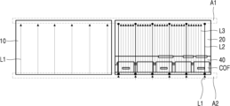
도 1은 설명의 편의를 위해 상부 기판(10)과 하부 기판(20)을 분리하여 전개한 도면을 함께 도시한다. 인쇄회로기판(40) 및 COF(Chip On Film)는 하부 기판(20)의 배면에 부착된다. 상부 기판(10)과 하부 기판(20)의 배면은 접착되어 고정될 수 있다.For convenience of explanation, FIG. 1 shows a separate developed view of the
도 2는 일 실시예에 따른 타일링 표시 장치의 단면도이다. 일례로, 도 2는 도 1의 하방 사이드 영역(A2)의 단면도이다.Figure 2 is a cross-sectional view of a tiling display device according to an embodiment. As an example, Figure 2 is a cross-sectional view of the lower side area A2 of Figure 1.
도 1 및 도 2를 참고하면, 일 실시예에 따른 마이크로 엘이디 표시 장치 및 타일링 표시 장치는 상부 기판(10) 및 하부 기판(20)을 포함한다. 상부 기판(10) 및 하부 기판(20)은 유리일 수 있다. 하지만, 이에 제한되지 않고, 상부 기판(10) 및 하부 기판(20)은 폴리이미드 등의 플렉서블한 재료일 수도 있다.Referring to FIGS. 1 and 2 , a micro LED display device and a tiling display device according to an embodiment include an
상부 기판(10)에는 마이크로 엘이디(12)와 박막 트랜지스터(11)가 실장되고 게이트 클럭 신호가 공급되는 게이트 클럭 라인(L1)이 배치된다. A
마이크로 엘이디(12)는 100㎛ 이하, 또는 웨이퍼가 제거된 상태의 엘이디일 수 있다. The
박막 트랜지스터(11)는 데이터 전압에 응답하여 구동하는 구동 트랜지스터 또는 에미션 신호에 응답하여 구동하는 에미션 트랜지스터일 수 있다. 구동 트랜지스터 및 에미션 트랜지스터는 전류 패스를 형성하여 마이크로 엘이디(12)에 전류를 전달하여 마이크로 엘이디(12)를 발광시킨다. 일례로, 마이크로 엘이디 표시 장치는 에미션 신호의 펄스 폭을 제어하여 전류 패스의 전류의 세기를 결정할 수 있다.The
상부 기판(10)과 하부 기판(20)은 라우팅(60)을 통해 연결된다. 상부 기판(10)과 하부 기판(20)은 각각 패드부(62)가 구비되고, 라우팅(60)은 상부 기판(10)의 패드부(62)과 하부 기판(20)의 패드부(62)를 연결한다.The
상부 기판(10)와 하부 기판(20) 사이에 도전성 접착체(30) 및 실란트(50)가 형성된다. 실란트(50)는 도전성 접착체(30)와 라우팅(60) 사이에 형성되어, 도전성 접착체(30)와 라우팅(60) 간을 절연한다. A
하부 기판(20)은 상부 기판(10)과 라우팅을 통해 연결되고 하부 기판(20)에는 전원 전압이 공급되는 전원 라인(L3)이 배치된다. 전원 전압은 기저 전압(EVSS) 또는 고전위 전압(EVDD)일 수 있다.The
일례로, 마이크로 엘이디 표시 장치는 발광부 역할을 하는 상부 기판(10)과 마이크로 엘이디 구동신호 생성을 위한 인쇄회로기판(40)이 실장되는 하부 기판(20)으로 이루어진 유닛 간 심레스 타일링(Seamless Tiling) 구현을 위해 내부는 도전성 접착제(30) 및 실란트(50) 중 적어도 하나 이상으로 고정된다.For example, a micro LED display device uses seamless tiling between units consisting of an
하부 기판(20)은 0V 전위를 보장하는 기저전압(EVSS) 신호 라인으로 배치되어 있으며, 상방 사이드 라우팅(Side Routing)을 통해 상부 기판(10)에 연결된다. 기저전압(EVSS) 외의 나머지 신호들은 모두 하방 사이드 라우팅을 통해 인쇄회로기판(40)에 연결된다. The
여기서, 상방 사이드 라우팅은 상방 사이드 영역(A1)에서 상부 기판(10)과 하부 기판(20)을 라우팅하는 것으로 정의될 수 있고, 하방 사이드 라우팅은 하방 사이드 영역(A2)에서 상부 기판(10)과 하부 기판(20)을 라우팅하는 것으로 정의될 수 있다.Here, the upper side routing can be defined as routing the
인쇄회로기판(40)에는 화소 회로를 구동하기 위한 구동 회로가 실장될 수 있고, COF에는 구동 회로의 신호를 표시 패널에 전달하는 신호 라인이 실장될 수 있다.A driving circuit for driving the pixel circuit may be mounted on the printed
하부 기판(20)에는 게이트 클럭 신호에 의해 발생되는 노이즈를 상쇄시키기 위한 의사 신호(Pseudo Signal)가 공급되는 의사 신호 라인(L2)이 배치된다.A pseudo signal line L2 is disposed on the
의사 신호는 하부 기판(20)의 의사 신호 라인(L2)에 공급되고, 상부 기판(10)의 게이트 클럭 라인(L1)에 공급되는 게이트 클럭 신호의 반전 신호와 동일한 패턴을 가진다. 의사 신호는 게이트 클럭 신호의 트랜지션(Transition) 구간에 발생하는 피크 전류를 감소시킴으로써 노이즈를 상쇄시킨다. The pseudo signal is supplied to the pseudo signal line L2 of the
일례로, 반전 신호 패턴은 게이트 클럭 신호 패턴을 반전시킨 패턴으로 설계될 수 있으며, 레벨시프터에서 출력되는 고전압 신호의 상쇄 신호로 이용될 수 있다. 일례로, 레벨시프터 출력의 반전 회로는 인쇄회로기판(40) 또는 하부 기판(20)에 설계될 수 있다. 반전 회로는 하부 기판(20)의 평면상에서 상방 사이드 영역(A1) 또는 하방 사이드 영역(A2)에 인접한 일측에 배치될 수 있다.For example, the inverted signal pattern can be designed as a pattern that inverts the gate clock signal pattern, and can be used as an offset signal for the high voltage signal output from the level shifter. For example, an inversion circuit for the level shifter output may be designed on the printed
도 3 내지 도 6은 일 실시예에 따른 마이크로 엘이디 표시 장치의 반전 회로를 예시한 도면이다.3 to 6 are diagrams illustrating an inversion circuit of a micro LED display device according to an embodiment.
도 3을 참고하면, 마이크로 엘이디 표시 장치는 게이트 클럭 신호를 반전시킨 신호를 의사 신호로서 의사 신호 라인(L2)에 공급하는 반전 회로(IV1)를 포함한다. Referring to FIG. 3, the micro LED display device includes an inverting circuit (IV1) that supplies a signal obtained by inverting the gate clock signal as a pseudo signal to the pseudo signal line (L2).
일례로, 반전 회로(IV1)는 마이크로 엘이디의 구동 신호들을 생성하는 인쇄회로기판(40)에 실장될 수 있다. 인쇄회로기판(40)의 게이트 클럭 생성 회로는 COF(Chip On Film)을 거쳐서 게이트 클럭 신호를 상부 기판(10)에 배치된 게이트 클럭 라인(L1)에 공급한다. For example, the inversion circuit IV1 may be mounted on the printed
인쇄회로기판(40)의 반전 회로(IV1)는 게이트 클럭 신호를 반전시킨 신호를 의사 신호로서 하부 기판(20)에 배치된 의사 신호 라인(L2)에 공급한다.The inversion circuit IV1 of the printed
다른 일례로, 도 4 및 도 5를 참고하면, 반전 회로(IV1)는 마이크로 엘이디의 구동 신호들을 생성하는 인쇄회로기판(40)과 의사 신호 라인(L2) 사이의 하부 기판(20)에 실장될 수 있다.As another example, referring to Figures 4 and 5, the inverting circuit (IV1) is mounted on the lower board (20) between the pseudo signal line (L2) and the printed circuit board (40) that generates the driving signals of the micro LED. You can.
일례로, 도 4에 도시한 바와 같이, 반전 회로(IV1)는 하부 기판(20)의 배면이면서 COF가 부착된 부분과 인접한 일측에 실장될 수 있다. 인쇄회로기판(40)의 게이트 클럭 생성 회로는 COF(Chip On Film)을 거쳐서 게이트 클럭 신호를 상부 기판(10)에 배치된 게이트 클럭 라인(L1)에 공급한다.For example, as shown in FIG. 4, the inversion circuit IV1 may be mounted on one side of the back of the
인쇄회로기판(40)의 게이트 클럭 생성 회로는 게이트 클럭 신호를 COF(Chip On Film)을 거쳐서 하부 기판(20)의 배면이면서 COF가 부착된 부분과 인접한 일측에 실장된 반전 회로(IV1)에 공급한다. 반전 회로(IV1)는 게이트 클럭 신호를 반전시킨 신호를 의사 신호로서 하부 기판(20)의 배면이면서 COF가 부착된 부분과 인접한 일측에서 의사 신호 라인(L2)에 공급한다. The gate clock generation circuit of the printed
다른 일례로, 도 5에 도시한 바와 같이, 반전 회로(IV1)는 하부 기판(20)의 배면이면서 상방 사이드 영역(A1)과 인접한 일측에 실장될 수 있다. 인쇄회로기판(40)의 게이트 클럭 생성 회로는 COF(Chip On Film)을 거쳐서 게이트 클럭 신호를 상부 기판(10)에 배치된 게이트 클럭 라인(L1)에 공급한다. As another example, as shown in FIG. 5, the inversion circuit IV1 may be mounted on the back of the
게이트 클럭 신호는 게이트 클럭 라인(L1)을 통해서 하부 기판(20)의 배면이면서 상방 사이드 영역(A1)에 인접한 일측에 실장된 반전 회로(IV1)에 공급된다. 반전 회로(IV1)는 게이트 클럭 신호를 반전시킨 신호를 의사 신호로서 하부 기판(20)의 상방에서 의사 신호 라인(L2)에 공급한다.The gate clock signal is supplied to the inverting circuit IV1 mounted on the rear side of the
또 다른 일례로, 도 6에 도시한 바와 같이, 상부 기판(10)의 게이트 클럭 라인(L1)과 연결되는 보조 게이트 클럭 라인(L1a)이 하부 기판(20)에 배치된다. 보조 게이트 클럭 라인(L1a)은 슬루 보상 회로(42)와 연결된다. 슬루 보상 회로(42)는 인쇄회로기판(40) 상에 배치될 수 있다.In another example, as shown in FIG. 6, an auxiliary gate clock line (L1a) connected to the gate clock line (L1) of the
슬루 보상 회로(42)는 보조 게이트 클럭 라인(L1a)으로부터 전달되는 게이트 클럭 신호를 센싱하고, 게이트 클럭 신호의 슬루(slew)를 고려하여 보완된 반전 신호 패턴을 의사 신호로서 의사 신호 라인(L2)에 공급한다. 일례로, 게이트 클럭 신호는 게이트 클럭 라인의 임피던스로 인해 라이징 에지 또는 폴링 에지 부분에 슬루가 형성될 수 있는데, 슬루 보상 회로(42)는 게이트 클럭 신호의 라이징 에지 또는 폴링 에지 부분에 형성되는 슬루(slew)를 고려하여 반전 신호 패턴을 생성할 수 있다.The
도 7은 일 실시예에 따른 마이크로 엘이디 표시 장치에서 게이트 클럭 신호와 의사 신호의 파형도이다. 도 8 및 도 9는 도 1의 의사 신호 라인의 터미네이션 패턴을 예시한 도면이다.Figure 7 is a waveform diagram of a gate clock signal and a pseudo signal in a micro LED display device according to an embodiment. Figures 8 and 9 are diagrams illustrating termination patterns of the pseudo signal lines of Figure 1.
도 7에 도시한 바와 같이, 게이트 클럭 신호(GCLK_n)는 게이트 클럭 라인의 임피던스를 고려하지 않은 이상적인 신호로 정의될 수 있고, 게이트 클럭 신호(GCLK_m)는 게이트 클럭 라인의 임피던스에 의해 라이징 및 폴링 에지 부분에 슬루를 가지는 신호로 정의될 수 있다.As shown in FIG. 7, the gate clock signal (GCLK_n) can be defined as an ideal signal without considering the impedance of the gate clock line, and the gate clock signal (GCLK_m) has rising and falling edges depending on the impedance of the gate clock line. It can be defined as a signal that has slew in the part.
의사 신호(Pseudo_n)는 게이트 클럭 신호(GCLK_n)의 반전 신호와 동일한 패턴을 가진다. 일례로, 의사 신호(Pseudo_n)는 상부 기판(10)의 게이트 클럭 신호(GCLK_n)와 반전된 동일한 라이징 및 폴링을 보장하도록 설계될 수 있다.The pseudo signal (Pseudo_n) has the same pattern as the inverted signal of the gate clock signal (GCLK_n). For example, the pseudo signal Pseudo_n may be designed to ensure the same rising and falling inverted as the gate clock signal GCLK_n of the
의사 신호(Pseudo_m)는 게이트 클럭 신호(GCLK_m)의 반전 신호와 동일한 패턴을 가진다. 일례로, 의사 신호(Pseudo_m)는 게이트 클럭 라인의 임피던스를 고려하여 게이트 클럭 신호(GCLK_m)와 반전된 동일한 라이징 및 폴링을 보장하도록 설계될 수 있다.The pseudo signal (Pseudo_m) has the same pattern as the inverted signal of the gate clock signal (GCLK_m). For example, the pseudo signal Pseudo_m may be designed to ensure the same inverted rising and falling as the gate clock signal GCLK_m by considering the impedance of the gate clock line.
다른 예로, 도 8 및 도 9에 도시한 바와 같이, 게이트 클럭 라인의 임피던스에 의한 게이트 클럭 신호의 슬루(slew)를 고려하여 의사 신호 라인(L2)의 터미네이션(termination)이 서펀트(Serpent) 패턴으로 형성될 수 있다. 여기서 터미네이션은 그라운드와 인접한 의사 신호 라인(L2)의 단부로 정의될 수 있다.As another example, as shown in FIGS. 8 and 9, considering the slew of the gate clock signal due to the impedance of the gate clock line, the termination of the pseudo signal line L2 is a serpent pattern. can be formed. Here, termination may be defined as the end of the pseudo signal line (L2) adjacent to the ground.
도 8과 같이, 의사 신호 라인(L2)의 단부는 펄스 형태의 서펀트 패턴(L2a)으로 형성될 수 있다. 또는 도 9와 같이 의사 신호 라인(L2)의 단부는 완만한 굴곡 형태의 서펀트 패턴(L2b)으로 형성될 수 있다.As shown in FIG. 8, the end of the pseudo signal line L2 may be formed as a pulse-shaped serpent pattern L2a. Alternatively, as shown in FIG. 9, the end of the pseudo signal line L2 may be formed as a gently curved serpent pattern L2b.
의사 신호 라인(L2)의 단부는 게이트 신호 라인의 임피던스에 따라 그 길이나 결정될 수 있고, 그 길이에 따라 서펀트 패턴(L2a) 또는 서펀트 패턴(L2b)으로 형성될 수 있다.The length of the end of the pseudo signal line L2 may be determined depending on the impedance of the gate signal line, and may be formed as a serpent pattern L2a or serpent pattern L2b depending on the length.
즉, 게이트 신호 라인의 임피던스에 따른 게이트 클럭 신호의 슬루를 고려하여 의사 신호 라인(L2)의 단부의 패턴을 보완 설계하여 의사 신호 라인의 임피던스를 게이트 신호 라인의 임피던스와 동일하도록 조절함으로써, 게이트 클럭 신호와 동일한 반전 신호를 의사 신호로서 얻을 수 있다. That is, by considering the slew of the gate clock signal according to the impedance of the gate signal line and designing the pattern at the end of the pseudo signal line (L2) to be complementary, the impedance of the pseudo signal line is adjusted to be the same as the impedance of the gate signal line, so that the gate clock An inverted signal identical to the signal can be obtained as a pseudo signal.
도 10은 일 실시예에 따른 마이크로 엘이디 표시 장치의 상방 사이드 영역의 단면도이다. 도 11은 일 실시예에 따른 마이크로 엘이디 표시 장치의 하방 사이드 영역의 단면도이다.Figure 10 is a cross-sectional view of the upper side area of a micro LED display device according to an embodiment. Figure 11 is a cross-sectional view of a lower side area of a micro LED display device according to an embodiment.
도 1, 도 10 및 도 11을 참고하면, 상부 기판(10)과 하부 기판(20)는 상방 사이드 영역(A1)의 상방 라우팅 및 하방 사이드 영역(A2)의 하방 라우팅을 통해 연결된다.Referring to FIGS. 1, 10, and 11, the
상방 사이드 영역(A1)은, 도 10에 도시한 바와 같이, 상방 사이드 영역(A1)의 상부 기판(10)과 하부 기판(20) 사이에 도전성 접착체(30)가 형성된다. In the upper side area A1, as shown in FIG. 10, a
도전성 접착체(30)는 상방 사이드 영역(A1)의 라우팅(60)을 통해 상부 기판(10)의 기저 전압 전극(80)과 하부 기판(20)의 기저 전압 전극(80)을 연결한다. 도전성 접착체(30)는 상방 사이드 영역(A1)의 상부 기판(10)과 하부 기판(20) 사이에서 리퍼런스 플레인 역할을 함으로써 상부 기판(10) 또는 하부 기판(20)의 기저 전압 전극(80)과 리퍼런스 플레인과의 거리를 기존 대비 반으로 줄일 수 있다. The
그리고, 하방 사이드 영역(A2)은, 도 11에 도시한 바와 같이, 상부 기판(10)와 하부 기판(20) 사이에 도전성 접착체(30) 및 실란트(50)가 형성된다. 실란트(50)는 도전성 접착체(30)와 하방 사이드 영역(A2)의 라우팅(60) 사이에 형성되어, 도전성 접착체(30)와 라우팅(60) 간을 절연한다. And, in the lower side area A2, as shown in FIG. 11, a
상부 기판(10)의 기저 전압 외의 신호 전극(90)과 하부 기판(20)의 기저 전압 외의 신호 전극(90)은 라우팅(60)을 통해서 연결된다. 라우팅(60)은 은(Ag)으로 형성될 수 있고, 라우팅(60)을 실링(sealing)하는 실링부(70)는 절연 물질로 형성될 수 있다. 라우팅(60)의 재료는 이에 제한되지 않고 도전성 물질로 형성될 수 있다. 예를 들어, 실링부(70)는 폴리에틸렌, 천연고무, 폴리에스텔, 에폭시수지, 합성 수지 등일 수 있다.The non-base
이와 같이 마이크로 엘이디의 리퍼런스 플레인(Reference Plane)이 강화되도록 설계된다. 리퍼런스 플레인은 그라운드와 연결되어 그라운드 플레인 역할을 한다. 상부 기판(10)과 하부 기판(20) 사이에 그라운드 플레인 역할을 하는 플레인을 추가 설계한다. 여기서, 그라운드 플레인은 상부 기판(10)의 전위 기준과 하부 기판(20)의 전위의 기준을 맞추는 역할을 한다. 또한, 그라운드 플레인은 상부 기판(10) 또는 하부 기판(20)에서 발생되는 EMI를 그라운드로 방출하는 역할을 한다. In this way, the reference plane of the micro LED is designed to be strengthened. The reference plane is connected to the ground and serves as a ground plane. A plane that serves as a ground plane is additionally designed between the
상방 사이드 영역(A1)은 상부 기판(10)과 하부 기판(20) 사이를 도전성 접착체(30) 및 실란트(50)로 반영하여 리퍼런스 플레인과의 거리를 L/2 보다 작게 줄일 수 있다. 여기서, L은 상부 기판(10)과 하부 기판(20)의 전극들 사이의 거리로 정의될 수 있다. The upper side area A1 can reduce the distance from the reference plane to less than L/2 by applying the
상부 기판(10)의 전극과 리퍼런스 플레인과의 거리를 또는 하부 기판(20)의 전극과 리퍼런스 플레인과의 거리를 줄임으로써 상부 기판(10)과 하부 기판(20)의 전위의 기준을 빠르게 설정할 수 있고, 상부 기판(10) 또는 하부 기판(20)에서 발생되는 EMI를 그라운드로 빠르게 방출할 수 있다. 상부 기판(10)과 하부 기판(20) 사이에 그라운드 플레인을 구비함으로써 EMI 개선 효과를 기대할 수 있다. 또한, 상방 사이드 라우팅 시 실란트(50)를 신호 전극(90)과 연결되도록 실링(Sealing)시 라우팅(60)과 접지 시킬 수 있다.By reducing the distance between the electrode of the
도 12는 일 실시예에 따른 타일링 표시 장치의 도면이다. Figure 12 is a diagram of a tiling display device according to an embodiment.
도 13은 도 12의 하나의 마이크로 엘이디 표시 장치를 도시한 도면이다. FIG. 13 is a diagram illustrating one micro LED display device of FIG. 12.
도 13은 설명의 편의를 위해 상부 기판(10)과 하부 기판(20)을 분리하여 전개한 도면이다. 인쇄회로기판(40) 및 COF는 하부 기판(20)의 배면에 부착된다. 상부 기판(10)과 하부 기판(20)의 배면은 접착되어 고정될 수 있다.FIG. 13 is a diagram in which the
도 14는 일 실시예에 따른 마이크로 엘이디 표시 장치에서 노이즈 상쇄를 설명하기 위한 파형도이다. Figure 14 is a waveform diagram for explaining noise cancellation in a micro LED display device according to an embodiment.
도 14에서, 기준 신호(Reference signal)는 시프트 레지스터에서 게이트 클럭 신호를 생성하는데 이용되는 기준 신호로 정의될 수 있다. 의사 신호(Pseudo Signal)는 게이트 클럭 신호의 트랜지션(Transition) 구간에 발생하는 피크 전류를 감소시켜 노이즈를 상쇄시키는데 이용되는 신호로 정의될 수 있다.In FIG. 14, a reference signal may be defined as a reference signal used to generate a gate clock signal in a shift register. A pseudo signal can be defined as a signal used to cancel out noise by reducing the peak current occurring in the transition section of the gate clock signal.
도 12 내지 도 14를 참고하면, 일 실시예에 따른 타일링 표시 장치는 제1 패널(B1), 제2 패널(B2), 제3 패널(B3), 제4 패널(B4) 및 제어 회로(FPGA, Field Programmable Gate Array)를 포함한다.Referring to FIGS. 12 to 14, the tiling display device according to one embodiment includes a first panel (B1), a second panel (B2), a third panel (B3), a fourth panel (B4), and a control circuit (FPGA). , Field Programmable Gate Array).
제어 회로(FPGA)는 제1 패널(B1)과 제3 패널(B3)에 기준 게이트 신호를 출력하고 제2 패널(B2)과 제4 패널(B4)에 타이밍이 지연된 게이트 클럭 신호를 출력한다.The control circuit (FPGA) outputs a reference gate signal to the first panel (B1) and the third panel (B3) and outputs a gate clock signal with delayed timing to the second panel (B2) and the fourth panel (B4).
제1 패널(B1), 제2 패널(B2), 제3 패널(B3) 및 제4 패널(B4) 각각은 상부 기판(10) 및 하부 기판(20)을 포함한다. 상부 기판(10) 및 하부 기판(20)은 라우팅(60)을 통해 연결된다. 라우팅(60)은 상방 라우팅과 하방 라우팅을 포함하고, 상방 라우팅은 상방 라우팅 영역(A1)에 배치되고 하방 라우팅은 하방 라우팅 영역(A1)에 배치된다. Each of the first panel B1, the second panel B2, the third panel B3, and the fourth panel B4 includes an
상부 기판(10) 및 하부 기판(20) 중 적어도 하나에는 기준 게이트 신호와 지연된 게이트 클럭 신호의 타이밍을 보상하는 분산 보상 회로(44)가 배치된다.A
분산 보상 회로(44)는 상부 기판(10)과 하부 기판(20)중 적어도 하나에 형성될 수 있다. 일례로, 분산 보상 회로(44)는 상방 사이드 영역의 라우팅과 인접한 상판 글래스(10)의 게이트 클럭 라인(L1)에 구비될 수 있다. 또는 분산 보상 회로(44)는 상방 사이드 영역의 라우팅과 인접한 하판 글래스(20)의 의사 신호 라인(L2)에 구비될 수 있다.The
상부 기판(10)에는 마이크로 엘이디가 실장되고 게이트 클럭 신호가 공급되는 게이트 클럭 라인(L1)이 배치된다. 하부 기판(20)에는 상부 기판(10)과 라우팅을 통해 연결되고 기저 전압이 공급되는 기저 전압 라인(L3)이 배치되며, 게이트 클럭 신호에 의해 발생되는 노이즈를 상쇄시키기 위한 의사 신호가 공급되는 의사 신호 라인(L2)이 배치된다.A micro LED is mounted on the
일례로, 하나의 제어 회로(FPGA)로 동작하는 두 개 이상 패널은 게이트 클럭 노이즈가 중첩하는 것을 방지하기 위해, 타이밍 분산 기술을 적용한다. 제어 회로(FPGA) 내 시프트 레지스터의 위상 보상 신호(PSC, Phase Shift Compensation CLK)를 추가하여 게이트 클럭 신호를 표시 패널에 공급한다.For example, two or more panels operating with one control circuit (FPGA) apply timing distribution technology to prevent gate clock noise from overlapping. The gate clock signal is supplied to the display panel by adding the phase compensation signal (PSC, Phase Shift Compensation CLK) of the shift register in the control circuit (FPGA).
제어 회로(FPGA)는 제1 패널(B1)과 제3 패널(B3)에 기준 게이트 신호를 출력하고 제2 패널(B2)과 제4 패널(B4)에 타이밍이 지연된 게이트 클럭 신호를 공급한다. 또는 제어 회로(FPGA)는 제1 패널(B1)과 제3 패널(B3)에 지연된 게이트 클럭 신호를 출력하고 제2 패널(B2)과 제4 패널(B4)에 기준 게이트 신호를 공급하여, 레벨 시프터의 출력 신호를 분산시킨다. 일례로, 제1 패널(B1)의 레벨 시프터는 기준 게이트 신호를 이용하여 출력 신호를 출력하고, 제2 패널(B2)의 레벨 시프터는 타이밍이 지연된 게이트 클럭 신호를 이용하여 출력 신호를 출력하므로, 출력 타이밍이 분산될 수 있다. The control circuit (FPGA) outputs a reference gate signal to the first panel (B1) and the third panel (B3) and supplies a gate clock signal with delayed timing to the second panel (B2) and the fourth panel (B4). Alternatively, the control circuit (FPGA) outputs a delayed gate clock signal to the first panel (B1) and the third panel (B3) and supplies a reference gate signal to the second panel (B2) and the fourth panel (B4) to level Distributes the output signal of the shifter. For example, the level shifter of the first panel (B1) outputs an output signal using a reference gate signal, and the level shifter of the second panel (B2) outputs an output signal using a gate clock signal with delayed timing, Output timing may be distributed.
분산 보상 회로(44)를 상부 기판(10) 및 하부 기판(20) 중 적어도 하나에 설계하여 타이밍 분산으로 인한 게이트 출력 타이밍 차이로 발생하는 화면 단차를 예방한다. 여기서, 화면 단차는 제1 패널(B1) 내지 제4 패널(B4)에서 표시되는 영상의 타이밍 차이로 예시될 수 있다.The
일례로, 분산 보상 회로(44)를 설계하여 상부 기판(10)의 게이트 클럭 라인(L1)에 보상된 시프트 레지스터 보상 신호를 공급한다. 예를 들면, 상부 기판(10) 내 더미 게이트 드라이버 블록 내 분산 보상 회로(44)를 추가할 수 있다. 또한, 하부 기판(20) 내 기저전압 신호 라인 일부를 삭제하고, 분산 보상 회로(44)를 설계할 수 있다.For example, a distributed
분산 보상 회로(44)는 기준 게이트 신호로부터 타이밍이 분산 및 지연된 게이트 클럭 신호의 타이밍을 보상하여 상판 글라스(10)의 게이트 클럭 라인(L1)에 공급한다. The
일례로, 분산 보상 회로(44)는 상방 사이드 영역의 라우팅과 인접한 상판 글래스(10)의 게이트 클럭 라인(L1)에 구비될 수 있다. 또는 분산 보상 회로(44)는 상방 사이드 영역의 라우팅과 인접한 하판 글래스(20)의 의사 신호 라인(L2)에 구비될 수 있다.For example, the
도 15는 일 실시예에 따른 마이크로 엘이디 표시 장치에서 게이트 신호 생성 장치의 블록도이다. 도 16은 도 15의 마이크로 엘이디 표시 장치에서 게이트 신호 생성 장치의 세부 블록도이다. 도 15 및 도 16는 레벨시프터 출력 신호의 타이밍 분산 기술을 나타낸다.Figure 15 is a block diagram of a gate signal generating device in a micro LED display device according to an embodiment. FIG. 16 is a detailed block diagram of a gate signal generating device in the micro LED display device of FIG. 15. Figures 15 and 16 show a timing distribution technique for the level shifter output signal.
도 15 및 도 16를 참고하면, 게이트 신호 생성 장치는 위상 시프트 필터(200), 제1 레벨 시프터(310), 제2 레벨 시프터(320), 제1 위상 보상 회로(410), 제2 위상 보상 회로(420), 제1 GIP(Gate In Panel) 회로(510) 및 제2 GIP 회로를 포함한다. 여기서, 제1 GIP 회로(510) 및 제2 GIP 회로는 시프트 레지스터로 구성될 수 있으며, 제1 시프트 레지스터(510) 및 제2 시프트 레지스터(520)로 명명될 수 있다.15 and 16, the gate signal generating device includes a
게이트 신호 생성 장치는 타이밍 컨트롤러(100)로부터 위상 보상 신호(PSC), 게이트 스타트 펄스(GSP), 게이트 클럭 신호(GCLK1), 및 마스터 클럭 신호(MCLK1)를 수신하고, 이를 기반으로 제1 게이트 신호(P_Gate Out1) 내지 제2160 게이트 신호(P_Gate Out2160)를 생성하여, 표시 패널의 게이트 라인들 각각에 순차적으로 출력한다.The gate signal generating device receives a phase compensation signal (PSC), a gate start pulse (GSP), a gate clock signal (GCLK1), and a master clock signal (MCLK1) from the
제1 레벨 시프터(310)는 타이밍 컨트롤러(100)로부터 위상 보상 신호(PSC), 게이트 스타트 펄스(GSP), 게이트 클럭 신호(GCLK1), 및 마스터 클럭 신호(MCLK1)를 수신한다. 제1 레벨 시프터(310)는 위상 보상 신호(PSC)를 제1 위상 보상 회로(410)에 전달하고, 게이트 스타트 펄스(GSP)에 응답하여 스타트 신호(VST) 및 리셋 신호(RST)를 제1 위상 보상 회로(410)에 출력한다. 제1 레벨 시프터(310)는 게이트 클럭 신호(GCLK1) 및 마스터 클럭 신호(MCLK1)를 기반으로 제1 클럭 신호(CLK1) 내지 제10 클럭 신호(CLK10)를 생성하고, 이를 제1 시프트 레지스터(510)에 출력한다.The
위상 시프트 필터(200)는 타이밍 컨트롤러(100)로부터 게이트 클럭 신호(GCLK1) 및 마스터 클럭 신호(MCLK1)를 수신하고, 이를 지연시키며, 지연된 게이트 클럭 신호(F_GCLK2) 및 지연된 마스터 클럭 신호(F_MCLK2)를 제2 레벨 시프터(320)에 출력한다.The
제2 레벨 시프터(320)는 타이밍 컨트롤러(100)로부터 위상 보상 신호(PSC), 게이트 스타트 펄스(GSP)를 수신한다. 제2 레벨 시프터(320)는 위상 보상 신호(PSC)를 제2 위상 보상 회로(420)에 전달하고, 게이트 스타트 펄스(GSP)에 응답하여 스타트 신호(VST) 및 리셋 신호(RST)를 제2 위상 보상 회로(420)에 출력한다. The
제2 레벨 시프터(320)는 지연된 게이트 클럭 신호(F_GCLK2) 및 지연된 마스터 클럭 신호(F_MCLK2)를 기반으로 제1 클럭 신호(CLK1) 내지 제10 클럭 신호(CLK10)를 생성하고, 이를 제2 시프트 레지스터(520)에 출력한다. 제2 레벨 시프터(320)로부터 출력되는 제1 클럭 신호(CLK1) 내지 제10 클럭 신호(CLK10)는 제1 레벨 시프터(310)로부터 출력되는 제1 클럭 신호(CLK1) 내지 제10 클럭 신호(CLK10)와 다른 위상을 가진다.The
제1 위상 보상 회로(410)는 위상 보상 신호(PSC)를 기반으로 스타트 신호(VST) 및 리셋 신호(RST)의 위상을 보상하여 보상 스타트 신호(P_VST) 및 보상 리셋 신호(P_RST)를 제1 시프트 레지스터(510)에 출력한다.The first
제2 위상 보상 회로(420)는 위상 보상 신호(PSC)를 기반으로 스타트 신호(VST) 및 리셋 신호(RST)의 위상을 보상하여 보상 스타트 신호(P_VST) 및 보상 리셋 신호(P_RST)를 제2 시프트 레지스터(520)에 출력한다.The second
제1 시프트 레지스터(510)는 보상 스타트 신호(P_VST)에 응답하여 제1 게이트 신호(P_Gate Out1) 내지 제2160 게이트 신호(P_Gate Out2160)를 순차적으로 출력한다. 제1 시프트 레지스터(510)는 보상 리셋 신호(P_RST)에 응답하여 내부 회로의 특정 노드를 기저전압 또는 전원전압으로 초기화한다.The
제2 시프트 레지스터(520)는 보상 스타트 신호(P_VST)에 응답하여 제1 게이트 신호(P_Gate Out1) 내지 제2160 게이트 신호(P_Gate Out2160)를 순차적으로 출력한다. 제2 시프트 레지스터(520)는 보상 리셋 신호(P_RST)에 응답하여 내부 회로의 특정 노드를 기저전압 또는 전원전압으로 초기화한다.The
게이트 신호 생성 장치는 제1 패널(B1) 내지 제4 패널(B4)들 각각의 좌측 및 우측에 구비될 수 있다. 게이트 신호 생성 장치는 게이트 클럭(레벨시프터 ~ 시프트 레지스터)의 위상을 조절하여 EMI를 분산시킨다. 제1 위상 보상 회로(410) 및 제2 위상 보상 회로(420)는 시프트 레지스터의 더미 스테이지에 구비될 수 있다. 일례로, 제1 시프트 레지스터(510) 및 제2 시프트 레지스터(520)는 보상 스타트 신호(P_VST)에 응답하여 순차적으로 구동하는 복수의 스테이지들을 포함할 수 있고, 복수의 스테이지들은 제1 게이트 신호(P_Gate Out1) 내지 제2160 게이트 신호(P_Gate Out2160)를 순차적으로 출력한다. The gate signal generating device may be provided on the left and right sides of each of the first to fourth panels B1 to B4. The gate signal generation device distributes EMI by adjusting the phase of the gate clock (level shifter ~ shift register). The first
여기서, 복수의 스테이지들 중 첫 번째 스테이지 및 마지막 번째 스테이지 중 적어도 하나는 더미 스테이지로 이용될 수 있다. 예를 들면, 첫 번째 스테이지가 더미 스테이지인 경우 두 번째 스테이지에 보상 스타트 신호(P_VST)를 출력할 수 있고, 마지막 번째 스테이지가 더미 스테이지인 경우 마지막 번째 이전 스테이지에 보상 스타트 신호(P_VST)를 출력할 수 있다. 즉, 시프트 레지스터 더미 스테이지에 위상 보상 회로를 구성하여 패널의 좌측 및 우측의 화면 단차를 예방한다.Here, at least one of the first stage and the last stage among the plurality of stages may be used as a dummy stage. For example, if the first stage is a dummy stage, the compensation start signal (P_VST) can be output to the second stage, and if the last stage is a dummy stage, the compensation start signal (P_VST) can be output to the last previous stage. You can. In other words, a phase compensation circuit is configured in the shift register dummy stage to prevent screen steps on the left and right sides of the panel.
T1 기간은 제1 레벨 시프터(310)과 제2 레벨 시프터(320) 간에 위상 차이를 발생시키는 기간이다. T2 기간은 제1 시프트 레지스터(510)과 제2 시프트 레지스터(520) 간에 위상이 동일하게 보상되는 기간이다.The T1 period is a period for generating a phase difference between the
타이밍 컨트롤러(100)는 게이트 스타트 펄스(GSP), 게이트 클럭 신호(GCLK1), 마스터 클럭 신호(MCLK1)과 함께 위상 보상 신호(PSC)를 제1 레벨 시프터(310)과 제2 레벨 시프터(320)에 제공한다. 타이밍 컨트롤러(100)와 제2 레벨 시프터(320) 사이에는 위상 시프트 필터(200, Phase Shift Filter)가 구비되어 지연된 게이트 클럭 신호(F_GCLK2), 지연된 마스터 클럭 신호(F_MCLK2)가 제2 레벨 시프터(320)에 제공된다.The
제1 레벨 시프터(310)와 제2 레벨 시프터(320)는 레벨 시프트된 제1 클럭 신호(CLK1) 내지 제2 클럭 신호(CLK10)를 제1 시프트 레지스터(510)와 제2 시프트 레지스터(520)에 제공한다.The
그리고, 제1 레벨 시프터(310)와 제2 레벨 시프터(320)는 위상 보상 신호(PSC)와 스타트 신호(VST) 및 리셋 신호(RST)를 제1 위상 보상 회로(410) 및 제2 위상 보상 회로(420)에 제공한다. 제1 위상 보상 회로(410) 및 제2 위상 보상 회로(420)는 스타트 신호(VST) 및 리셋 신호(RST)의 위상을 보상하고, 위상이 보상된 스타트 신호(P_VST) 및 리셋 신호(P_RST)를 제1 시프트 레지스터(510)과 제2 시프트 레지스터 (520)에 제공한다.And, the
제1 시프트 레지스터(510)와 제2 시프트 레지스터(520)는 위상이 보상된 보상 스타트 신호(P_VST) 및 보상 리셋 신호(P_RST)에 응답하여 위상이 보상된 제1 내지 제2160 게이트 신호(P_Gate Out1 ~ P_Gate Out2160)를 표시 패널의 게이트 라인들에 출력한다.The
일 실시예에 따른 마이크로 엘이디 표시 장치는, 패널 설계 측면에서, 게이트 클럭에 의한 노이즈를 상쇄하도록 설계된다. 하부 기판(20)에 상부 기판(10)의 게이트 클럭 라인(L1)과 동일한 의사 신호 라인(L2)을 배치한다. 그리고, 레벨시프터와 시프트 레지스터 간의 임피던스를 고려하여 의사 신호 라인의 형태를 구조화한다.A micro LED display device according to an embodiment is designed to cancel out noise caused by a gate clock in terms of panel design. A pseudo signal line (L2) identical to the gate clock line (L1) of the upper substrate (10) is disposed on the lower substrate (20). Also, the shape of the pseudo signal line is structured by considering the impedance between the level shifter and the shift register.
그리고, 의사 신호 라인(L2)의 경로가 안정화되도록 설계되고, 게이트 신호에 대한 타이밍 분산을 보상하도록 설계된다. 하부 기판(20)에 기준 게이트 신호로부터 타이밍이 분산 및 지연된 게이트 클럭 신호의 타이밍을 보상하여 상부 기판(10)의 게이트 클럭 라인(L1)에 공급하는 분산 보상 회로(44)를 설계한다. Additionally, the path of the pseudo signal line L2 is designed to be stable and to compensate for timing dispersion for the gate signal. A
또한, 일 실시예에 따른 마이크로 엘이디 표시 장치는, 기구 설계 측면에서, 상부 기판(10)와 하부 기판(20) 사이의 접착제와 실란트를 도전성으로 설계하여 그라운드 플레인(GND Plane) 역할을 하게 한다. 상방 사이드 라우팅 시 실란트를 접지 설계한다. In addition, in the micro LED display device according to one embodiment, in terms of mechanical design, the adhesive and sealant between the
또한, 일 실시예에 따른 마이크로 엘이디 표시 장치는, 회로 설계 측면에서, 인쇄회로기판(40) 및 기판 내 레벨시프터 출력의 반전 회로를 생성하여 상쇄 신호공급이 가능하도록 설계한다.In addition, in terms of circuit design, the micro LED display device according to one embodiment is designed to enable supply of an offset signal by generating an inversion circuit for the output of the level shifter within the printed
이와 같이, 일 실시예에 따른 마이크로 엘이디 표시 장치는, 마이크로 엘이디가 실장되고 게이트 클럭 신호가 공급되는 게이트 클럭 라인(L1)이 배치된 상부 기판(10) 및 상부 기판(10)과 라우팅을 통해 연결되고, 기저 전압이 공급되는 기저 전압 라인(L3)이 배치된 하부 기판(20)를 포함한다. 하부 기판(20)에 게이트 클럭 신호에 의해 발생되는 노이즈를 상쇄시키기 위한 의사 신호가 공급되는 의사 신호 라인(L2)이 배치된다.In this way, the micro LED display device according to one embodiment is connected to the
하부 기판(20)의 의사 신호 라인(L2)에 공급되는 의사 신호는 상부 기판(10)의 게이트 클럭 라인(L1)에 공급되는 게이트 클럭 신호의 반전 신호와 동일한 패턴을 가질 수 있다.The pseudo signal supplied to the pseudo signal line L2 of the
마이크로 엘이디 표시 장치는 게이트 클럭 신호를 반전시킨 신호를 의사 신호로서 의사 신호 라인(L2)에 공급하는 반전 회로(IV1)를 더 포함할 수 있다.The micro LED display device may further include an inverting circuit (IV1) that supplies a signal obtained by inverting the gate clock signal as a pseudo signal to the pseudo signal line (L2).
반전 회로(IV1)는 마이크로 엘이디의 구동 신호들을 생성하는 인쇄회로기판(40)에 형성될 수 있다.The inversion circuit IV1 may be formed on the printed
또는, 반전 회로(IV1)는 마이크로 엘이디의 구동 신호들을 생성하는 인쇄회로기판(40)과 의사 신호 라인(L2) 사이의 하부 기판(20)에 실장될 수 있다.Alternatively, the inversion circuit IV1 may be mounted on the
게이트 클럭 신호의 슬루(slew)를 고려하여 의사 신호 라인(L2)의 터미네이션(termination)이 서펀트(Serpent) 패턴으로 형성될 수 있다.Considering the slew of the gate clock signal, the termination of the pseudo signal line L2 may be formed in a serpent pattern.
상부 기판(10)의 게이트 클럭 라인(L1)과 연결되는 제2 게이트 클럭 라인(L1a)이 하부 기판(20)에 배치될 수 있다.A second gate clock line L1a connected to the gate clock line L1 of the
마이크로 엘이디 표시 장치는 제2 게이트 클럭 라인(L1a)으로부터 전달되는 게이트 클럭 신호를 센싱하고, 게이트 클럭 신호의 슬루를 보상한 반전 신호를 의사 신호로서 의사 신호 라인(L2)에 공급하는 슬루 보상 회로(42)를 더 포함할 수 있다.The micro LED display device includes a slew compensation circuit ( 42) may further be included.
상부 기판(10)와 하부 기판(20)는 상방 사이드 영역(A1)의 라우팅 및 하방 사이드의 영역(A2)의 라우팅을 통해 연결될 수 있다.The
상방 사이드 영역(A1)의 상부 기판(10)와 하부 기판(20)는 그 사이에 도전성 접착체(30)가 형성될 수 있다.A
도전성 접착체(30)는 상방 사이드 영역(A1)의 라우팅(60)을 통해 상부 기판(10)의 기전 전압 전극(80)과 하부 기판(10)의 기저 전압 전극(80)과 연결될 수 있다.The conductive adhesive 30 may be connected to the
하방 사이드 영역(A2)의 상부 기판(10)와 하부 기판(20)는 그 사이에 도전성 접착체(30) 및 실란트(50)가 형성될 수 있다.A
신란트(50)는 도전성 접착체(30)와 하방 사이드 영역(A2)의 라우팅(60) 사이에 형성될 수 있다.The
마이크로 엘이디 표시 장치는 기준 게이트 신호로부터 타이밍이 분산 및 지연된 게이트 클럭 신호의 타이밍을 보상하여 상부 기판(10)의 게이트 클럭 라인(L1)에 공급하는 분산 보상 회로(44)를 더 포함할 수 있다.The micro LED display device may further include a
분산 보상 회로(44)는 상방 사이드 영역(A1)의 라우팅과 인접한 상판 글래스(10)의 게이트 클럭 라인(L1)에 구비될 수 있다. 또는 분산 보상 회로(44)는 상방 사이드 영역(A1)의 라우팅과 인접한 하판 글래스(20)의 의사 신호 라인(L2)에 구비될 수 있다.The
일 실시예에 따른 마이크로 엘이디 표시 장치는, 제1 패널, 제2 패널 및 제1 패널에 기준 게이트 신호를 출력하고 제2 패널에 타이밍이 지연된 게이트 클럭 신호를 출력하는 제어 회로(FPGA)를 포함하고, 제1 패널 및 제2 패널 각각은 상부 기판(10) 및 상부 기판(10)와 라우팅을 통해 연결되는 하부 기판(20)를 포함한다. 상부 기판(10) 및 하부 기판(20) 중 적어도 하나에는 기준 게이트 신호와 지연된 게이트 클럭 신호의 타이밍을 보상하는 분산 보상 회로(44)가 배치된다.A micro LED display device according to an embodiment includes a first panel, a second panel, and a control circuit (FPGA) that outputs a reference gate signal to the first panel and a gate clock signal with delayed timing to the second panel, , each of the first panel and the second panel includes an
실시예들에 따르면, 마이크로 엘이디의 하부 기판(20) 내 저주파 대역 노이즈 저감을 위한 패턴과 회로를 설계하여 상부 기판(10)의 게이트 클럭 신호에 의한 EMI를 상쇄할 수 있다.According to embodiments, EMI caused by the gate clock signal of the
또한, 상부 기판(10)와 하부 기판(20) 사이에 도전성 접착제(30)를 적용하여 안정적인 전압 공급을 보장할 수 있다.Additionally, a stable voltage supply can be ensured by applying a conductive adhesive 30 between the
또한, 하부 기판(20)를 통해 위상 보상 신호를 공급하여 타이밍 분산에 따른 화면 단차를 예방할 수 있다.In addition, by supplying a phase compensation signal through the
또한, 마이크로 엘이디 유닛 내 패턴 설계의 구조적 한계 내에서 발광부의 동작에 간섭 없이 게이트 클럭 EMI를 저감할 수 있다.Additionally, within the structural limits of the pattern design within the micro LED unit, gate clock EMI can be reduced without interfering with the operation of the light emitting unit.
또한, 노이즈 중첩현상을 해소하기 위하여 적용되는 타이밍 분산기술에 대한 부작용을 제거할 수 있다.Additionally, side effects of the timing distribution technology applied to resolve the noise overlap phenomenon can be eliminated.
또한, 상부 기판과 하부 기판 사이에 그라운드 플레인 배치에 따른 EMI 개선 효과가 있다.Additionally, there is an EMI improvement effect due to the arrangement of the ground plane between the upper and lower substrates.
또한, 상부 기판(10)과 하부 기판(20) 사이에 고정을 위해 적용되어 있는 접착제 및 실란트 재질을 도전성으로 설계하여 그라운드 플레인을 확장할 수 있다.In addition, the ground plane can be expanded by designing the adhesive and sealant materials applied for fixation between the
이상과 같이 본 발명에 대해서 예시한 도면을 참조로 하여 설명하였으나, 본 명세서에 개시된 실시 예와 도면에 의해 본 발명이 한정되는 것은 아니며, 본 발명의 기술사상의 범위 내에서 통상의 기술자에 의해 다양한 변형이 이루어질 수 있음은 자명하다. 아울러 앞서 본 발명의 실시 예를 설명하면서 본 발명의 구성에 따른 작용 효과를 명시적으로 기재하여 설명하지 않았을 지라도, 해당 구성에 의해 예측 가능한 효과 또한 인정되어야 함은 당연하다.As described above, the present invention has been described with reference to the illustrative drawings, but the present invention is not limited to the embodiments and drawings disclosed herein, and various modifications may be made by those skilled in the art within the scope of the technical idea of the present invention. It is obvious that transformation can occur. In addition, although the operational effects according to the configuration of the present invention were not explicitly described and explained while explaining the embodiments of the present invention above, it is natural that the predictable effects due to the configuration should also be recognized.
10: 상부 기판
20: 하부 기판
30: 도전성 접착제
40: 인쇄회로기판
50: 실란트
60: 라우팅
70: 실링부
80: EVSS 전극
90: EVSS 외 신호 전극
L1: 게이트 클럭 라인
L2: 의사 신호 라인
L3: 기저 전압 라인
IV1: 반전 회로
42: 슬루 보상 회로
44: 분산 보상 회로10: upper substrate 20: lower substrate
30: Conductive adhesive 40: Printed circuit board
50: Sealant 60: Routing
70: sealing part 80: EVSS electrode
90: EVSS other signal electrode L1: Gate clock line
L2: pseudo signal line L3: base voltage line
IV1: Inverting circuit 42: Slew compensation circuit
44: Dispersion compensation circuit
Claims (20)
상기 상부 기판과 라우팅을 통해 연결되고, 기저 전압이 공급되는 기저 전압 라인이 배치된 하부 기판을 포함하고,
상기 하부 기판에 상기 게이트 클럭 신호에 의해 발생되는 노이즈를 상쇄시키기 위한 의사 신호(Pseudo Signal)가 공급되는 의사 신호 라인이 배치된, 마이크로 엘이디 표시 장치.An upper substrate on which a micro LED is mounted and a gate clock line to which a gate clock signal is supplied is arranged; and
a lower substrate connected to the upper substrate through routing and having a base voltage line supplied with a base voltage;
A micro LED display device in which a pseudo signal line for supplying a pseudo signal to cancel out noise generated by the gate clock signal is disposed on the lower substrate.
상기 하부 기판의 상기 의사 신호 라인에 공급되는 상기 의사 신호는 상기 상부 기판의 상기 게이트 클럭 라인에 공급되는 상기 게이트 클럭 신호의 반전 신호와 동일한 패턴을 가지는 마이크로 엘이디 표시 장치.According to claim 1,
The pseudo signal supplied to the pseudo signal line of the lower substrate has the same pattern as the inverted signal of the gate clock signal supplied to the gate clock line of the upper substrate.
상기 게이트 클럭 신호를 반전시킨 신호를 상기 의사 신호로서 상기 의사 신호 라인에 공급하는 반전 회로를 더 포함하는 마이크로 엘이디 표시 장치.According to claim 1,
A micro LED display device further comprising an inverting circuit that supplies a signal obtained by inverting the gate clock signal to the pseudo signal line as the pseudo signal.
상기 반전 회로는 상기 마이크로 엘이디의 구동 신호들을 생성하는 인쇄회로기판에 형성되는 마이크로 엘이디 표시 장치.According to claim 3,
The inverting circuit is a micro LED display device formed on a printed circuit board that generates driving signals of the micro LED.
상기 반전 회로는, 상기 마이크로 엘이디의 구동 신호들을 생성하는 인쇄회로기판과 상기 의사 신호 라인 사이의 상기 하부 기판에 실장되는 마이크로 엘이디 표시 장치.According to claim 3,
The inverting circuit is a micro LED display device mounted on the lower substrate between the pseudo signal line and a printed circuit board that generates driving signals of the micro LED.
상기 게이트 클럭 신호의 슬루(slew)를 고려하여 상기 의사 신호 라인의 터미네이션(termination)이 서펀트(Serpent) 패턴으로 형성되는 마이크로 엘이디 표시 장치.According to claim 1,
A micro LED display device in which termination of the pseudo signal line is formed in a serpent pattern in consideration of slew of the gate clock signal.
상기 상부 기판의 상기 게이트 클럭 라인과 연결되는 제2 게이트 클럭 라인이 상기 하부 기판에 배치 되는 마이크로 엘이디 표시 장치.According to claim 1,
A micro LED display device in which a second gate clock line connected to the gate clock line of the upper substrate is disposed on the lower substrate.
상기 제2 게이트 클럭 라인으로부터 전달되는 상기 게이트 클럭 신호를 센싱하고, 상기 게이트 클럭 신호의 슬루를 보상한 반전 신호를 상기 의사 신호로서 상기 의사 신호 라인에 공급하는 슬루 보상 회로를 더 포함하는 마이크로 엘이디 표시 장치.According to claim 7,
A micro LED display further comprising a slew compensation circuit that senses the gate clock signal transmitted from the second gate clock line and supplies an inverted signal that compensates for the slew of the gate clock signal to the pseudo signal line as the pseudo signal. Device.
상기 상부 기판과 상기 하부 기판은 상방 사이드 영역의 라우팅 및 하방 사이드 영역의 라우팅을 통해 연결되는 마이크로 엘이디 표시 장치.According to claim 1,
A micro LED display device wherein the upper substrate and the lower substrate are connected through routing in the upper side area and routing in the lower side area.
상기 상방 사이드 영역의 상기 상부 기판과 상기 하부 기판은 그 사이에 도전성 접착체가 형성되는 마이크로 엘이디 표시 장치.According to clause 9,
A micro LED display device in which a conductive adhesive is formed between the upper substrate and the lower substrate in the upper side area.
상기 도전성 접착체는 상기 상방 사이드 영역의 라우팅을 통해 상기 상부 기판의 기전 전압 전극과 상기 하부 기판의 기저 전압 전극과 연결되는 마이크로 엘이디 표시 장치.According to claim 10,
The conductive adhesive is connected to the electromotive voltage electrode of the upper substrate and the base voltage electrode of the lower substrate through routing in the upper side region.
상기 하방 사이드 영역의 상기 상부 기판과 상기 하부 기판은 그 사이에 도전성 접착체 및 절연 실란트가 형성되는 마이크로 엘이디 표시 장치.According to clause 9,
A micro LED display device in which a conductive adhesive and an insulating sealant are formed between the upper substrate and the lower substrate in the lower side area.
상기 절연 신란트는 상기 도전성 접착체와 상기 하방 사이드 영역의 라우팅 사이에 형성되는 마이크로 엘이디 표시 장치.According to claim 12,
The insulating cement is formed between the conductive adhesive and the routing of the lower side area.
기준 게이트 신호로부터 타이밍이 분산 및 지연된 게이트 클럭 신호의 타이밍을 보상하여 상기 상판 글라스의 상기 게이트 클럭 라인에 공급하는 분산 보상 회로를 더 포함하는 마이크로 엘이디 표시 장치.According to claim 1,
A micro LED display device further comprising a dispersion compensation circuit that compensates for the timing of a gate clock signal whose timing is dispersed and delayed from a reference gate signal and supplies the timing to the gate clock line of the top glass.
상기 분산 보상 회로는
상기 게이트 클럭 라인과 상기 의사 신호 라인 중 적어도 하나에 형성되는 마이크로 엘이디 표시 장치.According to claim 14,
The distributed compensation circuit is
A micro LED display device formed on at least one of the gate clock line and the pseudo signal line.
제2 패널; 및
상기 제1 패널에 기준 게이트 신호를 출력하고, 상기 제2 패널에 타이밍이 지연된 게이트 클럭 신호를 출력하는 제어 회로를 포함하고,
상기 제1 패널 및 제2 패널 각각은,
상부 기판 및
상기 상부 기판과 라우팅을 통해 연결되는 하부 기판을 포함하고,
상기 상부 기판 및 상기 하부 기판 중 적어도 하나에는 상기 기준 게이트 신호와 상기 지연된 게이트 클럭 신호의 타이밍을 보상하는 분산 보상 회로가 배치된 타일링 표시 장치.1st panel;
second panel; and
A control circuit that outputs a reference gate signal to the first panel and a gate clock signal with delayed timing to the second panel,
Each of the first panel and the second panel,
upper substrate and
It includes a lower substrate connected to the upper substrate through routing,
A tiling display device in which a dispersion compensation circuit that compensates for timing of the reference gate signal and the delayed gate clock signal is disposed on at least one of the upper substrate and the lower substrate.
상기 상부 기판에는 마이크로 엘이디가 실장되고, 게이트 클럭 신호가 공급되는 게이트 클럭 라인이 배치되며,
상기 하부 기판에는 상기 상부 기판과 라우팅을 통해 연결되고, 기저 전압이 공급되는 기저 전압 라인이 배치되며, 상기 게이트 클럭 신호에 의해 발생되는 노이즈를 상쇄시키기 위한 의사 신호가 공급되는 의사 신호 라인이 배치된, 타일링 표시 장치.According to claim 16,
A micro LED is mounted on the upper substrate, and a gate clock line to which a gate clock signal is supplied is disposed,
A base voltage line connected to the upper substrate through routing and supplied with a base voltage is disposed on the lower substrate, and a pseudo signal line supplied with a pseudo signal to cancel out noise generated by the gate clock signal is disposed. , tiling display device.
상기 하부 기판의 상기 의사 신호 라인에 공급되는 상기 의사 신호는 상기 상부 기판의 상기 게이트 클럭 라인에 공급되는 상기 게이트 클럭 신호의 반전 신호와 동일한 패턴을 가지는 타일링 표시 장치.According to claim 17,
A tiling display device wherein the pseudo signal supplied to the pseudo signal line of the lower substrate has the same pattern as an inverted signal of the gate clock signal supplied to the gate clock line of the upper substrate.
상기 게이트 클럭 신호를 반전시킨 신호를 상기 의사 신호로서 상기 의사 신호 라인에 공급하는 반전 회로를 더 포함하는 타일링 표시 장치.According to claim 19,
A tiling display device further comprising an inverting circuit that supplies a signal obtained by inverting the gate clock signal to the pseudo signal line as the pseudo signal.
상기 분산 보상 회로는
상기 상방 사이드 영역의 라우팅에 인접한 상기 게이트 클럭 라인과 상기 의사 신호 라인 중 적어도 하나에 구비되는 타일링 표시 장치.According to claim 17,
The distributed compensation circuit is
A tiling display device provided on at least one of the gate clock line and the pseudo signal line adjacent to the routing of the upper side area.
Priority Applications (4)
| Application Number | Priority Date | Filing Date | Title |
|---|---|---|---|
| KR1020220180320A KR20240098502A (en) | 2022-12-21 | 2022-12-21 | Micro led display apparatus and tiling display apparatus |
| US18/540,007 US12374272B2 (en) | 2022-12-21 | 2023-12-14 | Display device |
| DE102023135740.9A DE102023135740A1 (en) | 2022-12-21 | 2023-12-19 | DISPLAY DEVICE |
| CN202311748502.8A CN118230670A (en) | 2022-12-21 | 2023-12-19 | Display device |
Applications Claiming Priority (1)
| Application Number | Priority Date | Filing Date | Title |
|---|---|---|---|
| KR1020220180320A KR20240098502A (en) | 2022-12-21 | 2022-12-21 | Micro led display apparatus and tiling display apparatus |
Publications (1)
| Publication Number | Publication Date |
|---|---|
| KR20240098502A true KR20240098502A (en) | 2024-06-28 |
Family
ID=91434688
Family Applications (1)
| Application Number | Title | Priority Date | Filing Date |
|---|---|---|---|
| KR1020220180320A Pending KR20240098502A (en) | 2022-12-21 | 2022-12-21 | Micro led display apparatus and tiling display apparatus |
Country Status (4)
| Country | Link |
|---|---|
| US (1) | US12374272B2 (en) |
| KR (1) | KR20240098502A (en) |
| CN (1) | CN118230670A (en) |
| DE (1) | DE102023135740A1 (en) |
Families Citing this family (1)
| Publication number | Priority date | Publication date | Assignee | Title |
|---|---|---|---|---|
| TWI860215B (en) | 2023-04-13 | 2024-10-21 | 錼創顯示科技股份有限公司 | Multi-layer display module |
Family Cites Families (14)
| Publication number | Priority date | Publication date | Assignee | Title |
|---|---|---|---|---|
| US6849935B2 (en) * | 2002-05-10 | 2005-02-01 | Sarnoff Corporation | Low-cost circuit board materials and processes for area array electrical interconnections over a large area between a device and the circuit board |
| KR20060134373A (en) * | 2005-06-22 | 2006-12-28 | 엘지전자 주식회사 | Dual panel unit |
| KR101859475B1 (en) | 2011-10-04 | 2018-05-21 | 엘지디스플레이 주식회사 | Flat display device |
| GB2519587A (en) * | 2013-10-28 | 2015-04-29 | Barco Nv | Tiled Display and method for assembling same |
| US10468397B2 (en) * | 2017-05-05 | 2019-11-05 | X-Celeprint Limited | Matrix addressed tiles and arrays |
| CN118263235A (en) * | 2017-09-04 | 2024-06-28 | 首尔半导体株式会社 | Light-emitting device |
| TWI722405B (en) * | 2019-03-28 | 2021-03-21 | 佳世達科技股份有限公司 | Display pannel |
| US11211001B2 (en) * | 2020-05-22 | 2021-12-28 | Huayuan Semiconductor (Shenzhen) Limited Company | Display device with feedback via serial connections between distributed driver circuits |
| JP7574317B2 (en) * | 2020-11-18 | 2024-10-28 | 京セラ株式会社 | Wiring board and display device |
| KR20220069690A (en) | 2020-11-20 | 2022-05-27 | 삼성전자주식회사 | Display module, display apparatus and method for manufacturing the same |
| KR102907077B1 (en) | 2020-12-31 | 2025-12-31 | 엘지디스플레이 주식회사 | Display apparatus and multi screen display apparatus using the same |
| KR20240120248A (en) * | 2023-01-31 | 2024-08-07 | 엘지디스플레이 주식회사 | Display device |
| TW202436966A (en) * | 2023-03-06 | 2024-09-16 | 晶云科技股份有限公司 | Tiled display and manufacturing method thereof |
| TWI872483B (en) * | 2023-03-17 | 2025-02-11 | 友達光電股份有限公司 | Display panel, tiled display device including the same and manufacturing method thereof |
-
2022
- 2022-12-21 KR KR1020220180320A patent/KR20240098502A/en active Pending
-
2023
- 2023-12-14 US US18/540,007 patent/US12374272B2/en active Active
- 2023-12-19 DE DE102023135740.9A patent/DE102023135740A1/en active Pending
- 2023-12-19 CN CN202311748502.8A patent/CN118230670A/en active Pending
Also Published As
| Publication number | Publication date |
|---|---|
| US20240212586A1 (en) | 2024-06-27 |
| US12374272B2 (en) | 2025-07-29 |
| CN118230670A (en) | 2024-06-21 |
| DE102023135740A1 (en) | 2024-06-27 |
Similar Documents
| Publication | Publication Date | Title |
|---|---|---|
| KR102396469B1 (en) | Display device | |
| KR102636630B1 (en) | Display apparatus | |
| JP2011081372A (en) | Electronic device, display and control method of the same | |
| KR102659876B1 (en) | Shift register and display apparatus comprising the same | |
| US10854134B2 (en) | Source signal driving apparatus for display device | |
| CN103578394B (en) | Gate drive circuit and display device using the gate drive circuit | |
| JP3638123B2 (en) | Display module | |
| KR20190007727A (en) | Gate driving circuit and display dedvice using the same | |
| KR102203773B1 (en) | Display panel and Organic Light Emitting Diode display device using the same | |
| US10037738B2 (en) | Display gate driver circuits with dual pulldown transistors | |
| US20030030604A1 (en) | Liquid crystal display | |
| KR102455584B1 (en) | Organic Light Emitting Diode display panel and Organic Light Emitting Diode display device using the same | |
| TWI612508B (en) | Display device and data driver | |
| JPH11288339A (en) | Control circuit | |
| KR20240098502A (en) | Micro led display apparatus and tiling display apparatus | |
| KR100968564B1 (en) | Signal Processing Device and Method | |
| KR102433746B1 (en) | Gate drive integrated circuit and display device including the same | |
| KR102650352B1 (en) | Shift register and display device comprising the same | |
| GB2632031A (en) | Display device | |
| KR102381627B1 (en) | Display device | |
| CN117831437A (en) | Display device | |
| CN101546512A (en) | plasma display device | |
| KR102666874B1 (en) | Gate driver and organic light emitting display device including the same | |
| KR20240020613A (en) | Display panel and display device including the display panel | |
| CN118430408A (en) | Gate driver and display device including the same |
Legal Events
| Date | Code | Title | Description |
|---|---|---|---|
| PA0109 | Patent application |
St.27 status event code: A-0-1-A10-A12-nap-PA0109 |
|
| PG1501 | Laying open of application |
St.27 status event code: A-1-1-Q10-Q12-nap-PG1501 |
|
| P22-X000 | Classification modified |
St.27 status event code: A-2-2-P10-P22-nap-X000 |
|
| D11 | Substantive examination requested |
Free format text: ST27 STATUS EVENT CODE: A-1-2-D10-D11-EXM-PA0201 (AS PROVIDED BY THE NATIONAL OFFICE) |
|
| PA0201 | Request for examination |
St.27 status event code: A-1-2-D10-D11-exm-PA0201 |
|
| P22-X000 | Classification modified |
St.27 status event code: A-2-2-P10-P22-nap-X000 |