KR20240023276A - semiconductor package - Google Patents
semiconductor package Download PDFInfo
- Publication number
- KR20240023276A KR20240023276A KR1020220100709A KR20220100709A KR20240023276A KR 20240023276 A KR20240023276 A KR 20240023276A KR 1020220100709 A KR1020220100709 A KR 1020220100709A KR 20220100709 A KR20220100709 A KR 20220100709A KR 20240023276 A KR20240023276 A KR 20240023276A
- Authority
- KR
- South Korea
- Prior art keywords
- semiconductor chip
- chip
- redistribution substrate
- substrate
- semiconductor
- Prior art date
- Legal status (The legal status is an assumption and is not a legal conclusion. Google has not performed a legal analysis and makes no representation as to the accuracy of the status listed.)
- Pending
Links
Images


Classifications
-
- H—ELECTRICITY
- H01—ELECTRIC ELEMENTS
- H01L—SEMICONDUCTOR DEVICES NOT COVERED BY CLASS H10
- H01L25/00—Assemblies consisting of a plurality of semiconductor or other solid state devices
- H01L25/03—Assemblies consisting of a plurality of semiconductor or other solid state devices all the devices being of a type provided for in a single subclass of subclasses H10B, H10D, H10F, H10H, H10K or H10N, e.g. assemblies of rectifier diodes
- H01L25/04—Assemblies consisting of a plurality of semiconductor or other solid state devices all the devices being of a type provided for in a single subclass of subclasses H10B, H10D, H10F, H10H, H10K or H10N, e.g. assemblies of rectifier diodes the devices not having separate containers
- H01L25/065—Assemblies consisting of a plurality of semiconductor or other solid state devices all the devices being of a type provided for in a single subclass of subclasses H10B, H10D, H10F, H10H, H10K or H10N, e.g. assemblies of rectifier diodes the devices not having separate containers the devices being of a type provided for in group H10D89/00
- H01L25/0657—Stacked arrangements of devices
-
- H10W72/30—
-
- H—ELECTRICITY
- H01—ELECTRIC ELEMENTS
- H01L—SEMICONDUCTOR DEVICES NOT COVERED BY CLASS H10
- H01L23/00—Details of semiconductor or other solid state devices
- H01L23/28—Encapsulations, e.g. encapsulating layers, coatings, e.g. for protection
- H01L23/31—Encapsulations, e.g. encapsulating layers, coatings, e.g. for protection characterised by the arrangement or shape
- H01L23/3107—Encapsulations, e.g. encapsulating layers, coatings, e.g. for protection characterised by the arrangement or shape the device being completely enclosed
-
- H—ELECTRICITY
- H01—ELECTRIC ELEMENTS
- H01L—SEMICONDUCTOR DEVICES NOT COVERED BY CLASS H10
- H01L23/00—Details of semiconductor or other solid state devices
- H01L23/48—Arrangements for conducting electric current to or from the solid state body in operation, e.g. leads, terminal arrangements ; Selection of materials therefor
- H01L23/482—Arrangements for conducting electric current to or from the solid state body in operation, e.g. leads, terminal arrangements ; Selection of materials therefor consisting of lead-in layers inseparably applied to the semiconductor body (electrodes)
- H01L23/4824—Pads with extended contours, e.g. grid structure, branch structure, finger structure
-
- H—ELECTRICITY
- H01—ELECTRIC ELEMENTS
- H01L—SEMICONDUCTOR DEVICES NOT COVERED BY CLASS H10
- H01L24/00—Arrangements for connecting or disconnecting semiconductor or solid-state bodies; Methods or apparatus related thereto
- H01L24/01—Means for bonding being attached to, or being formed on, the surface to be connected, e.g. chip-to-package, die-attach, "first-level" interconnects; Manufacturing methods related thereto
- H01L24/02—Bonding areas ; Manufacturing methods related thereto
- H01L24/07—Structure, shape, material or disposition of the bonding areas after the connecting process
-
- H—ELECTRICITY
- H01—ELECTRIC ELEMENTS
- H01L—SEMICONDUCTOR DEVICES NOT COVERED BY CLASS H10
- H01L24/00—Arrangements for connecting or disconnecting semiconductor or solid-state bodies; Methods or apparatus related thereto
- H01L24/01—Means for bonding being attached to, or being formed on, the surface to be connected, e.g. chip-to-package, die-attach, "first-level" interconnects; Manufacturing methods related thereto
- H01L24/26—Layer connectors, e.g. plate connectors, solder or adhesive layers; Manufacturing methods related thereto
- H01L24/31—Structure, shape, material or disposition of the layer connectors after the connecting process
-
- H—ELECTRICITY
- H01—ELECTRIC ELEMENTS
- H01L—SEMICONDUCTOR DEVICES NOT COVERED BY CLASS H10
- H01L25/00—Assemblies consisting of a plurality of semiconductor or other solid state devices
- H01L25/18—Assemblies consisting of a plurality of semiconductor or other solid state devices the devices being of the types provided for in two or more different main groups of the same subclass of H10B, H10D, H10F, H10H, H10K or H10N
-
- H—ELECTRICITY
- H10—SEMICONDUCTOR DEVICES; ELECTRIC SOLID-STATE DEVICES NOT OTHERWISE PROVIDED FOR
- H10B—ELECTRONIC MEMORY DEVICES
- H10B80/00—Assemblies of multiple devices comprising at least one memory device covered by this subclass
-
- H10P72/74—
-
- H10W20/20—
-
- H10W70/09—
-
- H10W70/611—
-
- H10W70/614—
-
- H10W70/635—
-
- H10W70/65—
-
- H10W70/685—
-
- H10W72/072—
-
- H10W74/01—
-
- H10W74/014—
-
- H10W74/117—
-
- H10W90/00—
-
- H10W90/701—
-
- H—ELECTRICITY
- H01—ELECTRIC ELEMENTS
- H01L—SEMICONDUCTOR DEVICES NOT COVERED BY CLASS H10
- H01L2225/00—Details relating to assemblies covered by the group H01L25/00 but not provided for in its subgroups
- H01L2225/03—All the devices being of a type provided for in the same main group of the same subclass of class H10, e.g. assemblies of rectifier diodes
- H01L2225/04—All the devices being of a type provided for in the same main group of the same subclass of class H10, e.g. assemblies of rectifier diodes the devices not having separate containers
- H01L2225/065—All the devices being of a type provided for in the same main group of the same subclass of class H10
- H01L2225/06503—Stacked arrangements of devices
- H01L2225/06513—Bump or bump-like direct electrical connections between devices, e.g. flip-chip connection, solder bumps
-
- H—ELECTRICITY
- H01—ELECTRIC ELEMENTS
- H01L—SEMICONDUCTOR DEVICES NOT COVERED BY CLASS H10
- H01L2225/00—Details relating to assemblies covered by the group H01L25/00 but not provided for in its subgroups
- H01L2225/03—All the devices being of a type provided for in the same main group of the same subclass of class H10, e.g. assemblies of rectifier diodes
- H01L2225/04—All the devices being of a type provided for in the same main group of the same subclass of class H10, e.g. assemblies of rectifier diodes the devices not having separate containers
- H01L2225/065—All the devices being of a type provided for in the same main group of the same subclass of class H10
- H01L2225/06503—Stacked arrangements of devices
- H01L2225/06524—Electrical connections formed on device or on substrate, e.g. a deposited or grown layer
-
- H—ELECTRICITY
- H01—ELECTRIC ELEMENTS
- H01L—SEMICONDUCTOR DEVICES NOT COVERED BY CLASS H10
- H01L2225/00—Details relating to assemblies covered by the group H01L25/00 but not provided for in its subgroups
- H01L2225/03—All the devices being of a type provided for in the same main group of the same subclass of class H10, e.g. assemblies of rectifier diodes
- H01L2225/04—All the devices being of a type provided for in the same main group of the same subclass of class H10, e.g. assemblies of rectifier diodes the devices not having separate containers
- H01L2225/065—All the devices being of a type provided for in the same main group of the same subclass of class H10
- H01L2225/06503—Stacked arrangements of devices
- H01L2225/06527—Special adaptation of electrical connections, e.g. rewiring, engineering changes, pressure contacts, layout
-
- H—ELECTRICITY
- H01—ELECTRIC ELEMENTS
- H01L—SEMICONDUCTOR DEVICES NOT COVERED BY CLASS H10
- H01L2225/00—Details relating to assemblies covered by the group H01L25/00 but not provided for in its subgroups
- H01L2225/03—All the devices being of a type provided for in the same main group of the same subclass of class H10, e.g. assemblies of rectifier diodes
- H01L2225/04—All the devices being of a type provided for in the same main group of the same subclass of class H10, e.g. assemblies of rectifier diodes the devices not having separate containers
- H01L2225/065—All the devices being of a type provided for in the same main group of the same subclass of class H10
- H01L2225/06503—Stacked arrangements of devices
- H01L2225/06541—Conductive via connections through the device, e.g. vertical interconnects, through silicon via [TSV]
-
- H—ELECTRICITY
- H01—ELECTRIC ELEMENTS
- H01L—SEMICONDUCTOR DEVICES NOT COVERED BY CLASS H10
- H01L2225/00—Details relating to assemblies covered by the group H01L25/00 but not provided for in its subgroups
- H01L2225/03—All the devices being of a type provided for in the same main group of the same subclass of class H10, e.g. assemblies of rectifier diodes
- H01L2225/04—All the devices being of a type provided for in the same main group of the same subclass of class H10, e.g. assemblies of rectifier diodes the devices not having separate containers
- H01L2225/065—All the devices being of a type provided for in the same main group of the same subclass of class H10
- H01L2225/06503—Stacked arrangements of devices
- H01L2225/06548—Conductive via connections through the substrate, container, or encapsulation
-
- H10P72/7424—
-
- H10P72/743—
-
- H10W70/60—
-
- H10W70/652—
-
- H10W72/01—
-
- H10W72/823—
-
- H10W72/877—
-
- H10W74/019—
-
- H10W74/15—
-
- H10W90/20—
-
- H10W90/28—
-
- H10W90/297—
-
- H10W90/722—
-
- H10W90/724—
-
- H10W90/732—
-
- H10W90/792—
Landscapes
- Engineering & Computer Science (AREA)
- Microelectronics & Electronic Packaging (AREA)
- Power Engineering (AREA)
- Computer Hardware Design (AREA)
- Physics & Mathematics (AREA)
- Condensed Matter Physics & Semiconductors (AREA)
- General Physics & Mathematics (AREA)
- Production Of Multi-Layered Print Wiring Board (AREA)
- Structures Or Materials For Encapsulating Or Coating Semiconductor Devices Or Solid State Devices (AREA)
Abstract
Description
본 발명은 반도체 패키지에 관한 것으로, 상세하게는 복수의 반도체 칩을 하나의 패키지로 구성한 반도체 패키지 및 그 제조 방법에 관한 것이다.The present invention relates to a semiconductor package, and more specifically, to a semiconductor package comprising a plurality of semiconductor chips in one package and a method of manufacturing the same.
반도체 패키지는 집적회로 칩을 전자제품에 사용하기 적합한 형태로 구현한 것이다. 통상적으로 반도체 패키지는 인쇄회로기판 상에 반도체 칩을 실장하고 본딩 와이어 내지 범프를 이용하여 이들을 전기적으로 연결하는 것이 일반적이다. 전자 산업의 발달로 반도체 패키지의 신뢰성 향상, 고집적화, 및 소형화를 위한 다양한 연구가 진행되고 있다.A semiconductor package is an integrated circuit chip implemented in a form suitable for use in electronic products. Typically, a semiconductor package mounts a semiconductor chip on a printed circuit board and electrically connects them using bonding wires or bumps. With the development of the electronics industry, various researches are being conducted to improve the reliability, high integration, and miniaturization of semiconductor packages.
본 발명이 해결하고자 하는 과제는 전기적 특성이 향상된 반도체 패키지를 제공하는 것에 있다.The problem to be solved by the present invention is to provide a semiconductor package with improved electrical characteristics.
본 발명에 해결하고자 하는 다른 과제는 집적도가 향상된 반도체 패키지를 제공하는 것에 있다.Another problem to be solved by the present invention is to provide a semiconductor package with improved integration.
본 발명이 해결하고자 하는 과제는 이상에서 언급한 과제에 제한되지 않으며, 언급되지 않은 또 다른 과제들은 아래의 기재로부터 당업자에게 명확하게 이해될 수 있을 것이다.The problem to be solved by the present invention is not limited to the problems mentioned above, and other problems not mentioned will be clearly understood by those skilled in the art from the description below.
본 발명의 실시예에 따른 반도체 패키지는 제1 재배선 기판, 상기 제1 재배선 기판 상에 배치되는 제2 재배선 기판, 상기 제1 재배선 기판과 상기 제2 재배선 기판 사이에 배치되는 칩 스택, 상기 제1 재배선 기판과 상기 제2 재배선 기판 사이에서 상기 칩 스택을 둘러싸는 제1 몰딩막 및 상기 제1 몰딩막을 수직으로 관통하여 상기 제1 재배선 기판과 상기 제2 재배선 기판을 연결하는 관통 전극을 포함할 수 있다. 상기 칩 스택은 상기 제1 재배선 기판에 실장되고 내부에 관통 비아를 포함하는 제1 반도체 칩, 상기 제1 반도체 칩 상에서 상기 관통 비아와 접속되는 제2 반도체 칩을 포함하는 칩 구조체 및 상기 제2 재배선 기판에 실장되는 제3 반도체 칩을 포함하되, 상기 제1 반도체 칩의 측면과 상기 칩 구조체의 측면은 공면(coplanar)을 이룰 수 있다.A semiconductor package according to an embodiment of the present invention includes a first redistribution substrate, a second redistribution substrate disposed on the first redistribution substrate, and a chip disposed between the first redistribution substrate and the second redistribution substrate. A stack, a first molding film surrounding the chip stack between the first redistribution substrate and the second redistribution substrate, and a first molding film vertically penetrating the first molding film to form the first redistribution substrate and the second redistribution substrate. It may include a penetrating electrode connecting the. The chip stack includes a first semiconductor chip mounted on the first redistribution substrate and including a through via therein, a chip structure including a second semiconductor chip connected to the through via on the first semiconductor chip, and the second semiconductor chip. It includes a third semiconductor chip mounted on a redistribution substrate, where a side surface of the first semiconductor chip and a side surface of the chip structure may be coplanar.
본 발명의 다른 실시예에 따른 반도체 패키지는 제1 재배선 기판, 상기 제1 재배선 기판 상에 실장되고 내부에 관통 비아를 포함하는 제1 반도체 칩 및 상기 제1 반도체 칩 상에 실장되고 제2 반도체 칩을 포함하는 칩 구조체, 상기 칩 구조체 상에 배치되는 제3 반도체 칩, 상기 제3 반도체 칩 상에 배치되는 제2 재배선 기판, 상기 제1 재배선 기판과 상기 제2 재배선 기판을 연결하는 연결 구조체 및 상기 제1 반도체 칩, 상기 칩 구조체 및 상기 제3 반도체 칩을 둘러싸는 제1 몰딩막을 포함할 수 있다. 상기 제2 재배선 기판은 절연층 및 상기 절연층 내의 배선 패턴들을 포함하고, 상기 제3 반도체 칩은 그의 상단에 칩 패드를 포함할 수 있다. 상기 배선 패턴들의 일부는 상기 제1 몰딩막 및 상기 절연층을 관통하여 상기 제3 반도체 칩의 상기 칩 패드에 연결될 수 있다.A semiconductor package according to another embodiment of the present invention includes a first redistribution substrate, a first semiconductor chip mounted on the first redistribution substrate and including a through via therein, and a second semiconductor chip mounted on the first semiconductor chip and A chip structure including a semiconductor chip, a third semiconductor chip disposed on the chip structure, a second redistribution substrate disposed on the third semiconductor chip, and connecting the first redistribution substrate and the second redistribution substrate. It may include a connection structure and a first molding film surrounding the first semiconductor chip, the chip structure, and the third semiconductor chip. The second redistribution substrate may include an insulating layer and wiring patterns within the insulating layer, and the third semiconductor chip may include a chip pad on top thereof. Some of the wiring patterns may penetrate the first molding film and the insulating layer and be connected to the chip pad of the third semiconductor chip.
본 발명의 다른 실시예에 따른 반도체 패키지는 제1 재배선 기판, 상기 제1 재배선 기판 상에 배치되는 제2 재배선 기판, 상기 제1 재배선 기판과 상기 제2 재배선 기판 사이에 제공되는 칩 스택, 상기 제1 재배선 기판과 상기 제2 재배선 기판 사이에서 상기 칩 스택을 둘러싸는 제1 몰딩막 및 상기 제1 몰딩막을 수직으로 관통하여 상기 제1 재배선 기판과 상기 제2 재배선 기판을 연결하는 관통 전극을 포함할 수 있다. 상기 칩 스택은 상기 제1 재배선 기판에 실장되고, 그의 내부를 수직으로 관통하는 관통 비아를 갖는 제1 반도체 칩, 상기 제1 반도체 칩 상에 상기 관통 비아와 접속하는 제2 반도체 칩, 상기 제1 반도체 칩 상에서 상기 제2 반도체 칩을 둘러싸는 제2 몰딩막 및 상기 제2 반도체 칩 및 상기 제2 몰딩막 상에 배치되며, 상기 제2 재배선 기판에 실장되는 제3 반도체 칩을 포함할 수 있다.A semiconductor package according to another embodiment of the present invention includes a first redistribution substrate, a second redistribution substrate disposed on the first redistribution substrate, and provided between the first redistribution substrate and the second redistribution substrate. A chip stack, a first molding layer surrounding the chip stack between the first redistribution substrate and the second redistribution substrate, and a first molding layer vertically penetrating the first redistribution substrate and the second redistribution layer. It may include a penetrating electrode connecting the substrate. The chip stack is mounted on the first redistribution substrate and includes a first semiconductor chip having a through via vertically penetrating its interior, a second semiconductor chip connected to the through via on the first semiconductor chip, and the first semiconductor chip. 1 may include a second molding film surrounding the second semiconductor chip on a semiconductor chip, and a third semiconductor chip disposed on the second semiconductor chip and the second molding film and mounted on the second redistribution substrate. there is.
본 발명의 실시예들에 따른 반도체 패키지는 3차원 집적회로를 구성하는 제1 반도체 칩 및 제2 반도체 칩, 및 그 상단에 제3 반도체 칩이 기판 사이에 차례로 적층되어 있을 수 있다. 따라서, 반도체 패키지의 집적도가 향상될 수 있다. The semiconductor package according to embodiments of the present invention may have a first semiconductor chip, a second semiconductor chip, and a third semiconductor chip on top of the first semiconductor chip constituting a three-dimensional integrated circuit, sequentially stacked between the substrates. Accordingly, the integration degree of the semiconductor package can be improved.
또한, 적층된 반도체 칩들의 최상단에 배치된 제3 반도체 칩은 제3 반도체 칩 상에 제공되는 재배선 기판과 직접 전기적으로 연결될 수 있으며, 이를 통해 제3 반도체 칩과 재배선 기판 사이의 전기적 연결 거리를 짧게 할 수 있다. 따라서, 반도체 패키지의 전기적 특성이 향상될 수 있다.In addition, the third semiconductor chip disposed at the top of the stacked semiconductor chips can be directly electrically connected to the redistribution substrate provided on the third semiconductor chip, and through this, the electrical connection distance between the third semiconductor chip and the redistribution substrate is shortened. can be shortened. Accordingly, the electrical characteristics of the semiconductor package can be improved.
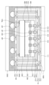
도 1은 본 발명의 실시예들에 따른 반도체 패키지의 단면도이다.
도 2은 본 발명의 실시예들에 따른 도 1의 B 영역을 확대한 단면도이다.
도 3는 본 발명의 실시예들에 따른 반도체 패키지의 평면도이다.
도 4는 본 발명의 실시예들에 따른 반도체 패키지의 단면도이다.
도 5 내지 도 15은 본 발명의 실시예들에 따른 반도체 패키지의 제조 방법을 설명하기 위한 단면도이다.
도 16 및 도 17은 본 발명의 실시예들에 따른 반도체 패키지의 제조 방법을 설명하기 위한 단면도이다.
도 18 및 도 19는 본 발명의 실시예들에 따른 반도체 패키지의 단면도이다. 1 is a cross-sectional view of a semiconductor package according to embodiments of the present invention.
Figure 2 is an enlarged cross-sectional view of area B of Figure 1 according to embodiments of the present invention.
3 is a plan view of a semiconductor package according to embodiments of the present invention.
4 is a cross-sectional view of a semiconductor package according to embodiments of the present invention.
5 to 15 are cross-sectional views for explaining a method of manufacturing a semiconductor package according to embodiments of the present invention.
16 and 17 are cross-sectional views for explaining a method of manufacturing a semiconductor package according to embodiments of the present invention.
18 and 19 are cross-sectional views of semiconductor packages according to embodiments of the present invention.
이하, 도면들 참조하여 본 발명의 개념에 따른 반도체 패키지를 설명한다.Hereinafter, a semiconductor package according to the concept of the present invention will be described with reference to the drawings.
도 1은 본 발명의 실시예들에 따른 반도체 패키지를 설명하기 위한 단면도이다. 도 2는 본 발명의 실시예들에 따른 도 1의 B 영역을 확대한 단면도이다. 도 3는 본 발명의 실시예들에 따른 반도체 패키지를 설명하기 위한 평면도이다. 1 is a cross-sectional view illustrating a semiconductor package according to embodiments of the present invention. Figure 2 is an enlarged cross-sectional view of area B of Figure 1 according to embodiments of the present invention. Figure 3 is a plan view for explaining a semiconductor package according to embodiments of the present invention.
도 1 내지 3을 참조하면, 반도체 패키지(10)는 제1 재배선 기판(110)을 포함할 수 있다. 제1 재배선 기판(110)은 평면적 관점에서 엣지 영역 및 센터 영역을 가질 수 있다. 제1 재배선 기판(110)의 상기 엣지 영역은 상기 센터 영역 및 제1 재배선 기판(110)의 측면 사이에 제공될 수 있다. 즉, 제1 재배선 기판(110)의 상기 센터 영역은 제1 재배선 기판(110)의 중심 상의 영역일 수 있으며, 제1 재배선 기판(110)의 상기 엣지 영역은 상기 센터 영역을 둘러싸는 영역일 수 있다. 제1 재배선 기판(110)은 제1 절연층들(112) 및 제1 배선 패턴들(113)을 포함할 수 있다.Referring to FIGS. 1 to 3 , the
제1 재배선 기판(110)의 제1 절연층들(112)은 상호 적층될 수 있다. 제1 절연층들(112)은 예를 들어, 감광성 절연(Photo-imageable dielectric, PID) 물질과 같은 유기 물질을 포함할 수 있다. 상기 감광성 절연 물질은 폴리머일 수 있다. 상기 감광성 절연 물질은 예를 들어, 감광성 폴리이미드, 폴리벤조옥사졸, 페놀계 폴리머, 및 벤조시클로부텐계 폴리머 중에서 적어도 하나를 포함할 수 있다. 도 1에서는 제1 절연층들(112) 간의 경계를 표시하였으나, 본 발명이 이에 한정되는 것은 아니다. 다른 실시예들에 따르면, 인접한 제1 절연층들(112) 사이의 계면은 구분되지 않을 수 있다.The first
제1 절연층들(112) 내에 제1 배선 패턴들(113)이 제공될 수 있다. 제1 배선 패턴들(113) 각각은 서로 일체로 연결된 제1 비아 부분 및 제1 배선 부분을 가질 수 있다. 상기 제1 배선 부분은 제1 재배선 기판(110) 내의 수평적 연결을 위한 패턴일 수 있다. 상기 제1 비아 부분은 제1 절연층들(112) 내에 제1 배선 패턴들(113)을 수직으로 연결하는 부분일 수 있다. 상기 제1 배선 부분은 상기 제1 비아 부분 상에 제공될 수 있다. 상기 제1 배선 부분은 상기 제1 비아 부분과 경계면 없이 연결될 수 있다. 상기 제1 배선 부분의 너비는 상기 제1 비아 부분의 너비보다 클 수 있다. 즉, 제1 배선 패턴들(113) 각각은 T 형상의 단면을 가질 수 있다. 제1 배선 패턴들(113)의 상기 제1 배선 부분은 제1 절연층들(112)의 상면 상에 위치할 수 있다. 제1 배선 패턴들(113)의 상기 제1 비아 부분은 제1 절연층들(112)을 관통하여 그 아래 배치되는 다른 제1 배선 패턴들(113)의 상기 제1 배선 부분에 접속될 수 있다. 제1 배선 패턴들(113)은 도전 물질을 포함할 수 있다. 예를 들면, 제1 배선 패턴들(113)은 구리(Cu)를 포함할 수 있다.
도시하지는 않았으나, 제1 배선 패턴들(113)의 하면들 상에 씨드 패턴들이 각각 배치될 수 있다. 예를 들면, 상기 씨드 패턴들은 각각 대응되는 제1 배선 패턴들(113)의 상기 제1 비아 부분의 하면, 측벽 및 상기 제1 배선 부분의 하면을 덮을 수 있다. 상기 씨드 패턴들은 제1 배선 패턴들(113)과 다른 물질을 포함할 수 있다. 예를 들어, 상기 씨드 패턴들은 구리(Cu), 타이타늄(Ti) 또는 이들의 합금을 포함할 수 있다. 상기 씨드 패턴들은 배리어층의 기능을 하며, 제1 배선 패턴들(113)에 포함된 물질의 확산을 방지할 수 있다.Although not shown, seed patterns may be disposed on the lower surfaces of the
제1 배선 패턴들(113) 중 최상단에 배치되는 제1 배선 패턴들(113)의 일부는 제1 재배선 기판(110)의 제1 재배선 패드들(114)일 수 있다. 예를 들어, 제1 배선 패턴들(113)의 상기 일부는 제1 재배선 기판(110)의 상면 상에 노출될 수 있다. 제1 재배선 패드들(114)은 서로 옆으로 이격되어 있을 수 있다. 제1 재배선 패드들(114)은 제1 배선 패턴들(113)에 접속될 수 있다. 제1 재배선 패드들(114)은 제1 재배선 기판(110)의 상면 상으로 돌출될 수 있다. 제1 재배선 패드들(114)은 상기 센터 영역에서 제1 반도체 칩(210)을 실장하기 위한 제1 재배선 패드들(114a) 및 상기 엣지 영역의 제1 재배선 패드들(114b)를 포함할 수 있다. 제1 재배선 패드들(114)은 도전 물질을 포함할 수 있다. 예를 들면, 제1 재배선 패드들(114)은 구리(Cu)를 포함할 수 있다.A portion of the
제1 절연층들(112) 중 최하단의 제1 절연층(112) 아래에 제1 기판 패드들(115)이 제공될 수 있다. 제1 기판 패드들(115)은 서로 옆으로 이격되어 있을 수 있다. 제1 기판 패드들(115)은 제1 배선 패턴들(113)과 접속될 수 있다. 예를 들어, 최하단의 제1 배선 패턴(113)의 상기 제1 비아 부분은 제1 절연층(112)을 관통하여 제1 기판 패드들(115)에 연결될 수 있다. 제1 기판 패드들(115)은 제1 배선 패턴들(113)을 통해 제1 재배선 패드들(114)와 접속될 수 있다. 제1 기판 패드들(115)과 제1 재배선 패드들(114)는 수직적으로 정렬되지 않을 수 있다. 제1 기판 패드들(115)은 도전 물질을 포함할 수 있다. 예를 들어 제1 기판 패드들(115)은 구리(Cu)를 포함할 수 있다.
제1 절연층들(112) 중 상기 최하단의 제1 절연층(112) 아래에 보호막(111)이 제공될 수 있다. 보호막(111)은 상기 최하단의 제1 절연층(112)의 하면 상에서 제1 기판 패드들(115)을 둘러쌀 수 있다. 제1 기판 패드들(115)의 하면은 보호막에 의해 덮이지 않을 수 있다. 보호막(111)은 솔더 레지스트(solder resist) 물질을 포함할 수 있다.A
외부 연결 단자들(600)이 제1 재배선 기판(110)의 하면 상에 배치될 수 있다. 외부 연결 단자들(600)은 노출되는 제1 기판 패드들(115)의 하면에 제공될 수 있다. 외부 연결 단자들(600)은 서로 옆으로 이격되어 있을 수 있다. 외부 연결 단자들(600)은 제1 기판 패드들(115)에 각각 접속될 수 있다. 외부 연결 단자들(600)은 제1 기판 패드들(115)을 통해 제1 배선 패턴들(113)과 전기적으로 연결될 수 있다. 외부 연결 단자들(600)은 솔더(solder) 물질을 포함할 수 있다. 예를 들면, 외부 연결 단자들(600)은 주석(Sn), 비스무트(Bi), 납(Pb), 은(Ag), 또는 이들의 합금을 포함할 수 있다.
제1 재배선 기판(110) 상에 칩 스택(200)이 제공될 수 있다. 칩 스택(200)은 제1 재배선 기판(110) 상에 순차적으로 적층되는 제1 반도체 칩(210), 칩 구조체 및 제3 반도체 칩(230)을 포함할 수 있다. 이하, 칩 스택(200)의 구성에 대해 보다 상세히 설명하도록 한다.A
제1 반도체 칩(210)이 제1 재배선 기판(110) 상에 배치될 수 있다. 제1 반도체 칩(210)이 제1 재배선 기판(110) 상에 실장될 수 있다. 제1 반도체 칩(210)은 제1 재배선 기판(110)의 상면 상에 배치될 수 있다. 제1 반도체 칩(210)은 예를 들어, 평면적 관점에서 제1 재배선 기판(110)의 상기 센터 영역 상에 배치될 수 있다. 제1 반도체 칩(210)은 제1 재배선 기판(110) 상에 페이스 다운(face down)으로 배치될 수 있다. 예를 들어, 제1 반도체 칩(210)은 제1 재배선 기판(110)을 향하는 전면 및 상기 전면과 대항하는 후면을 가질 수 있다. 이하, 본 명세서에서 전면이라 함은 반도체 칩 내의 집적 소자의 활성면(active surface) 측의 일면으로, 반도체 칩의 패드들이 형성되는 면으로 정의되고, 후면이라 함은 상기 전면에 대향되는 반대면일 수 있다. 제1 반도체 칩(210)의 상면은 후면에 해당할 수 있으며, 제1 반도체 칩(210)의 하면은 전면에 해당할 수 있다. 예를 들어, 제1 반도체 칩(210)은 그의 전면이 제1 재배선 기판(110)을 향하도록 배치될 수 있다. 제1 반도체 칩(210)은 일 예로, 로직 칩 또는 버퍼 칩일 수 있다. 상기 로직 칩은 ASIC칩 또는 어플리케이션 프로세서(AP) 칩을 포함할 수 있다. 또는, 상기 로직 칩은 중앙처리장치(Central Processing Unit, CPU) 또는 그래픽스 처리 장치(Graphic Processing Unit, GPU)를 포함할 수 있다. 상기 ASIC칩은 응용 주문형 집적 회로(application specific integrated circuit, ASIC)를 포함할 수 있다. 다른 예로, 제1 반도체 칩(210)은 메모리 칩일 수 있다.The
제1 반도체 칩(210)은 하부 칩 패드들(211), 관통 비아들(213) 및 상부 칩 패드들(212)을 포함할 수 있다. 하부 칩 패드들(211)은 제1 반도체 칩(210)의 하면 상에 제공될 수 있다. 하부 칩 패드들(211)은 제1 반도체 칩(210)의 하부에 형성되는 집적 회로들과 직접 연결될 수 있다. 상부 칩 패드들(212)은 제1 반도체 칩(210)의 상면 상에 제공될 수 있다. 하부 칩 패드들(211) 또는 상부 칩 패드들(212)은 제1 반도체 칩(210)의 칩 패드들일 수 있다. 관통 비아들(213)은 제1 반도체 칩(210)을 수직으로 관통하여 하부 칩 패드들(211) 및 상부 칩 패드들(212)을 연결할 수 있다. 상부 칩 패드들(212)은 관통 비아들(213)을 통해 하부 칩 패드들(211)과 전기적으로 연결될 수 있다. 본 명세서에서 어떤 구성 요소가 반도체 칩과 전기적으로 연결된다는 것은 반도체 칩의 칩 패드들을 통해 집적 회로들과 전기적으로 연결되는 것을 의미할 수 있다. 두 구성 요소들이 서로 전기적으로 연결되는 것은 직접적인 연결 또는 다른 구성 요소를 통한 간접적인 연결을 포함할 수 있다. 관통 비아들(213)은 금속을 포함할 수 있다. 예를 들어, 관통 비아들(213)은 구리(Cu)를 포함할 수 있다.The
제1 반도체 칩(210)은 플립 칩(flip chip) 방식으로 제1 재배선 기판(110)에 실장될 수 있다. 제1 칩 연결 단자들(214)이 제1 반도체 칩(210)의 하부 칩 패드들(211)의 하면에 제공될 수 있다. 제1 칩 연결 단자들(214)은 제1 반도체 칩(210)과 제1 재배선 패드들(114a) 사이에 개재될 수 있다. 예를 들어, 제1 칩 연결 단자들(214)은 제1 반도체 칩(210)과 제1 재배선 패드들(114a) 사이에 제공되어, 각각 대응되는 제1 반도체 칩(210)의 하부 칩 패드들(211) 및 제1 재배선 패드들(114a)에 접속될 수 있다. 이에 따라, 제1 반도체 칩(210)은 제1 칩 연결 단자들(214)을 통해 제1 재배선 기판(110)과 전기적으로 연결될 수 있다. 제1 칩 연결 단자들(214)은 도전 물질을 포함할 수 있다. 예를 들어, 제1 칩 연결 단자들(214)은 구리(Cu)를 포함할 수 있다.The
제1 반도체 칩(210) 상에 칩 구조체가 배치될 수 있다. 상기 칩 구조체는 제2 반도체 칩(220) 및 제2 몰딩막(410)을 포함할 수 있다.A chip structure may be disposed on the
제2 반도체 칩(220)이 제1 반도체 칩(210) 상에 배치될 수 있다. 제2 반도체 칩(220)은 제1 반도체 칩(210)과 다른 종류의 반도체 칩일 수 있다. 제2 반도체 칩(220)은 일 예로, 로직 칩 또는 버퍼 칩일 수 있다. 다른 예로, 제2 반도체 칩(220)은 메모리 칩일 수 있다. 제2 반도체 칩(220)의 폭 및 평면 형상은 제1 반도체 칩(210)의 폭 및 평면 형상보다 작을 수 있다. 제2 반도체 칩(220)은 상기 센터 영역에서 제1 반도체 칩(210)의 적어도 일부와 수직적으로 중첩될 수 있다. 일 예로, 제2 반도체 칩(220)의 전체는 제1 반도체 칩(210)과 수직적으로 중첩될 수 있으며, 평면적 관점에서 제2 반도체 칩(220)은 제1 반도체 칩(210)의 내측에 위치할 수 있다. 제2 반도체 칩(220)은 제2 반도체 칩(220)의 하면에 제공되는 제1 칩 패드들(221)을 포함할 수 있다. 제2 반도체 칩(220)은 서로 대향되는 전면 및 후면을 포함할 수 있다. 제2 반도체 칩(220)은 그의 전면이 제1 재배선 기판(110)을 향하도록 배치될 수 있다. The
제2 반도체 칩(220)은 플립 칩(flip chip) 방식으로 제1 반도체 칩(210) 상에 실장될 수 있다. 제2 칩 연결 단자들(222)은 제2 반도체 칩(220)의 제1 칩 패드들(221) 하면 상에 제공될 수 있다. 제2 칩 연결 단자들(222)은 제2 반도체 칩(220)의 제1 칩 패드들(221)에 접속될 수 있다. 제2 칩 연결 단자들(222)은 제1 반도체 칩(210) 및 제2 반도체 칩(220) 사이에 개재될 수 있다. 제2 칩 연결 단자들(222)은 제1 반도체 칩(210)의 상부 칩 패드들(212)에 접속될 수 있다. 이에 따라, 제2 반도체 칩(220)이 제1 반도체 칩(210)이 전기적으로 연결될 수 있다. 제2 칩 연결 단자들(222)는 도전 물질을 포함할 수 있다. 예를 들어, 제2 칩 연결 단자들(222)는 구리(Cu)를 포함할 수 있다.The
제2 몰딩막(410)이 제1 반도체 칩(210) 상에 제공될 수 있다. 제2 몰딩막(410)은 제2 반도체 칩(220)의 아래에서 제2 칩 연결 단자들(222)을 둘러쌀 수 있다. 제2 몰딩막(410)은 제2 반도체 칩(220)의 상면을 제외한 측면들 및 하면을 덮을 수 있다. 예를 들어, 제2 몰딩막(410)은 제2 반도체 칩(220)의 상기 측면들로부터 제2 반도체 칩(220)과 제1 반도체 칩(210) 사이 공간으로 연장될 수 있다. 제2 몰딩막(410)은 제1 반도체 칩(210)과 제2 반도체 칩(220) 사이에서 제2 칩 연결 단자들(222)을 둘러쌀 수 있다. 제2 몰딩막(410)은 제1 반도체 칩(210)의 상면과 접할 수 있다. 제2 몰딩막(410)의 측면은 제1 반도체 칩(210)의 측면과 공면(coplanar)을 이룰 수 있다. 이와는 다르게 제2 몰딩막(410)은 제2 반도체 칩(220)의 측면에 제공되지 않을 수 있으며, 제2 몰딩막(410)은 제2 반도체 칩(220)과 제1 반도체 칩(210)의 사이에만 제공될 수 있다. 이 경우, 제2 반도체 칩(220)의 폭 및 평면 형상은 제1 반도체 칩(210)의 폭 및 평면 형상과 실질적으로 동일할 수 있으며, 제1 반도체 칩(210)의 측면 및 제2 반도체 칩(220)의 측면은 공면(coplanar)을 이룰 수 있다 본 발명에 실시예들에 따르면 제1 반도체 칩(210), 제2 반도체 칩(220) 및 제2 몰딩막(410)은 3차원 집적회로(3D Integrated circuit)를 구성할 수 있다. 제2 몰딩막(410)은 에폭시계 몰딩 컴파운드와 같은 절연성 폴리머를 포함할 수 있다.A
제3 반도체 칩(230)이 상기 칩 구조체 상에 배치될 수 있다. 제3 반도체 칩(230)은 서로 대향되는 상면 및 하면을 포함할 수 있다. 제3 반도체 칩(230)의 상면은 활성면인 전면일 수 있다. 제3 반도체 칩(230)의 하면은 후면일 수 있다. 제3 반도체 칩(230)의 후면은 제2 반도체 칩(220)을 향할 수 있다. 다르게 설명하자면, 제2 반도체 칩(220)과 제3 반도체 칩(230)은 그들의 후면들이 서로 마주하는 백투백(back to back) 형태로 배치될 수 있다. 제3 반도체 칩(230)의 전면은 제2 반도체 칩(220)을 향하는 방향과 반대되는 방향을 향할 수 있다. 일 예로, 제3 반도체 칩(230)의 전면은 후술되는 제2 재배선 기판(120)을 향할 수 있다. 제3 반도체 칩(230)은 제3 반도체 칩(230)의 상면에 제공되는 제2 칩 패드들(231)을 포함할 수 있다. 제2 칩 패드들(231)은 제3 반도체 칩(230)의 상기 상면으로부터 노출될 수 있다. 본 발명의 실시예들에 따르면 3차원 집적 회로를 구성하는 제1 반도체 칩(210) 및 제2 반도체 칩(220)의 상단에 제3 반도체 칩(230)이 적층되어 집적도가 향상된 반도체 패키지를 구현할 수 있다. 제3 반도체 칩(230)의 측면은 제1 반도체 칩(210)의 측면 및 상기 칩 구조체의 측면과 정렬될 수 있다. 그러나, 본 발명이 이에 한정되는 것은 아니다. 제3 반도체 칩(230)의 폭 및 평면 형상은 제1 반도체 칩(210)의 폭 및 평면 형상 그리고 상기 칩 구조체의 폭 및 평면 형상과 다를 수 있다.A
제2 반도체 칩(220)의 평면 형상에 따라, 도시된 바와 다르게, 제1 반도체 칩(210), 제2 반도체 칩(220) 및 제3 반도체 칩(230)의 측면들은 수직으로 정렬될 수 있다. 제1 반도체 칩(210), 제2 반도체 칩(220) 및 제3 반도체 칩(230)의 너비는 각각 같을 수 있다. 이와는 다르게, 제1 반도체 칩(210), 제2 반도체 칩(220) 및 제3 반도체 칩(230)는 너비 및 크기는 필요에 따라 다르게 제공될 수 있다. Depending on the planar shape of the
제3 반도체 칩(230)이 상기 칩 구조체에 접착될 수 있다. 예를 들어, 제3 반도체 칩(230)의 하면 상에 접착 부재(430)가 제공될 수 있다. 접착 부재(430)는 제3 반도체 칩(230)의 하면 및 상기 칩 구조체의 상면 사이에 개재될 수 있다. 보다 상세하게는, 접착 부재(430)는 제3 반도체 칩(230)의 상기 하면에 제공될 수 있으며, 제2 반도체 칩(220)의 상면 및 제2 몰딩막(410)의 상면에 접착될 수 있다. 제3 반도체 칩(230)의 하면 및 제2 반도체 칩(220)의 상면은 접착 부재(430)을 사이에 두고 이격될 수 있다. 접착 부재(430)은 접착성 물질을 포함할 수 있다. 접착 부재(430)은 접착 필름일 수 있다. 접착 부재(430)은 에폭시(epoxy)를 포함할 수 있다.A
제1 반도체 칩(210), 제2 반도체 칩(220) 및 제3 반도체 칩(230)은 제1 재배선 기판(110)과 상에 차례로 적층되어 있을 수 있다. 제1 반도체 칩(210), 제2 반도체 칩(220) 및 제3 반도체 칩(230)은 수직적으로 중첩되는 적어도 일부를 포함할 수 있다. 중첩되는 상기 일부는 제1 반도체 칩(210), 제2 반도체 칩(220) 및 제3 반도체 칩(230) 모두가 중첩되는 영역일 수 있다. 도시한 바에 따르면, 제2 반도체 칩(220) 및 제3 반도체 칩(230)은 하나의 반도체 칩으로 제공되어 있으나 본 발명은 이에 한정되지 않으며, 필요에 따라 제2 반도체 칩(220) 및 제3 반도체 칩(230)은 옆으로 이격되어 있는 두 개 이상의 반도체 칩을 포함할 수 있다.The
제1 몰딩막(420)이 제1 재배선 기판(110) 상에 배치될 수 있다. 제1 몰딩막(420)은 제1 재배선 기판(110) 상에서 칩 스택(200)을 둘러쌀 수 있다. 보다 상세하게는, 제1 몰딩막(420)은 제1 반도체 칩(210)의 측면들, 상기 칩 구조체의 측면들 및 제3 반도체 칩(230)의 측면들을 덮을 수 있다. 제1 몰딩막(420)은 칩 스택(200)과 제1 재배선 기판(110) 사이의 공간을 채울 수 있다. 예를 들어, 제1 몰딩막(420)은 칩 스택(200)과 제1 재배선 기판(110) 사이에서 제1 칩 연결 단자들(214)을 둘러쌀 수 있다. 실시예들에서, 제1 몰딩막(420)은 칩 스택(200)을 덮을 수 있다. 예를 들어, 제1 몰딩막(420)은 제3 반도체 칩(230)의 상면을 덮을 수 있다. 제1 몰딩막(420)의 측면은 제1 재배선 기판(110)의 측면들과 수직으로 정렬될 수 있다. 제1 몰딩막(420)은 에폭시계 몰딩 컴파운드와 같은 절연성 폴리머를 포함할 수 있다. 제1 몰딩막(420)은 제2 몰딩막(410)과 동일 또는 상이한 물질을 포함할 수 있다.The
관통 전극들(300)이 제1 재배선 기판(110) 상에 제공될 수 있다. 관통 전극들(300)은 제1 재배선 기판(110) 상에서 칩 스택(200)으로부터 수평으로 이격될 수 있다. 예를 들어, 관통 전극들(300)은 제1 재배선 기판(110)의 상기 엣지 영역 상에 배치될 수 있다. 관통 전극들(300)은 평면적 관점에서 칩 스택(200)을 둘러쌀 수 있다. 관통 전극들(300)은 칩 스택(200)의 측면과 이격되어 배치될 수 있다.
관통 전극들(300)은 제1 몰딩막(420)을 수직으로 관통하여 제1 재배선 기판(110)에 연결될 수 있다. 예를 들어, 관통 전극들(300)은 제1 재배선 기판(110)의 제1 재배선 패드들(114b)에 접속될 수 있다. 관통 전극들(300)은 제1 재배선 기판(110)을 통해 외부 연결 단자들(600), 제1 반도체 칩(210) 및 제2 반도체 칩(220)과 전기적으로 연결될 수 있다.The through
관통 전극들(300)은 복수로 제공되며, 제1 재배선 기판(110) 상에서 서로 이격될 수 있다. 평면적 관점에서, 관통 전극들(300)은 제1 반도체 칩(210), 제2 반도체 칩(220) 및 제3 반도체 칩(230) 둘러싸도록 배열될 수 있다. 관통 전극들(300)은 제1 재배선 기판(110)과 후술되는 제2 재배선 기판(120)을 연결하는 연결 구조체일 수 있다. 관통 전극들(300)의 상면은 제1 몰딩막(420)의 상면으로 노출될 수 있다. 관통 전극들(300) 각각의 상면의 레벨은 제3 반도체 칩(230)의 상면의 레벨과 동일하거나 더 높을 수 있다. 관통 전극들(300) 각각은 원기둥 형상을 가질 수 있다. 그러나, 관통 전극들(300)의 형상은 다양하게 변형될 수 있으며, 다각형의 기둥 형상일 수 있다. 관통 전극들(300)의 폭은 제1 재배선 기판(110)으로부터 거리와 무관하게 균일할 수 있다. 이와는 다르게, 관통 전극들(300)의 폭은 제1 재배선 기판(110)을 향할수록 좁아질 수 있다. 관통 전극들(300)은 금속 물질을 포함할 수 있다. 예를 들어, 관통 전극들(300)은 구리(Cu) 또는 텅스텐(W)을 포함할 수 있다. A plurality of through
관통 전극들(300)이 복수로 제공됨에 따라, 열 전달 경로가 다양화될 수 있으며, 관통 전극들(300)에 의한 수직 방향으로의 열 전달 효율이 보다 향상될 수 있다. 도시된 바와는 다르게, 관통 전극들(300)은 칩 스택(200)의 측면들을 따라 연장되는 복수의 벽들일 수 있다. As a plurality of through
제2 재배선 기판(120)이 제1 몰딩막(420) 및 관통 전극들(300) 상에 제공될 수 있다. 제2 재배선 기판(120)이 제1 몰딩막(420) 및 관통 전극들(300)의 상면을 덮을 수 있다. 제2 재배선 기판(120)은 제2 절연층들(122) 및 제2 배선 패턴들(123)을 포함할 수 있다.A
제2 재배선 기판(120)은 적층된 제2 절연층들(122)을 포함할 수 있다. 제2 절연층들(122)은 제1 몰딩막(420) 상에 적층될 수 있다. 제2 절연층들(122) 각각은 서로 동일한 물질을 포함할 수 있다. 제2 절연층들(122)은 예를 들어, 감광성 절연(PID) 물질과 같은 유기 물질을 포함할 수 있다. 감광성 절연 물질은 폴리머일 수 있다. 감광성 절연 물질은 예를 들어, 감광성 폴리이미드, 폴리벤조옥사졸, 페놀계 폴리머, 및 벤조시클로부텐계 폴리머 중에서 적어도 하나를 포함할 수 있다. 제2 절연층들(122) 사이의 계면은 구분되지 않을 수 있으며, 제2 절연층들(122)이 적층되어 있는 수는 다양하게 변형될 수 있다.The
제2 배선 패턴들(123)이 제2 절연층들(122) 내에 제공될 수 있다. 제2 배선 패턴들(123) 각각은 서로 일체로 연결된 제2 비아 부분 및 제2 배선 부분을 가질 수 있다. 상기 제2 배선 부분은 제2 재배선 기판(120) 내의 수평적 연결을 위한 패턴일 수 있다. 상기 제2 비아 부분은 제2 절연층들(122) 내에 제2 배선 패턴들(123)을 수직으로 연결하는 부분일 수 있다. 상기 제2 배선 부분은 상기 제2 비아 부분 상에 제공될 수 있다. 상기 제2 배선 부분은 상기 제2 비아 부분과 경계면 없이 연결될 수 있다. 상기 배선 부분의 너비는 상기 제2 비아 부분의 너비보다 클 수 있다. 즉, 제2 배선 패턴들(123) 각각은 T 형상의 단면을 가질 수 있다. 제2 배선 패턴들(123)의 상면, 즉 상기 제2 배선 부분의 상면은 제2 절연층들(122)의 상면 상에 위치할 수 있다. 제2 배선 패턴들(123)의 하면, 즉 상기 제2 비아 부분의 하면은 제2 절연층들(122)을 관통하여 그 아래 배치되는 다른 제2 배선 패턴(123)의 상기 제2 배선 부분에 접속될 수 있다. 제2 배선 패턴들(123)은 도전 물질을 포함할 수 있다. 예를 들면, 제2 배선 패턴들(123)은 구리(Cu)를 포함할 수 있다.
제2 배선 패턴들(123) 중 최하단의 제2 배선 패턴들(123)은 관통 전극들(300)의 상면과 접할 수 있다. 제2 배선 패턴들(123) 중 일부 제2 배선 패턴들(123a)은 제2 재배선 기판(120)의 하면 상으로 돌출될 수 있다. 제2 배선 패턴들(123) 중 상기 일부 제2 배선 패턴들(123a)은 제3 반도체 칩(230)을 향해 연장되어 있을 수 있다. 예를 들어, 상기 일부 제2 배선 패턴들(123a)의 상기 제2 비아 부분은 최하단의 제2 절연층(122) 및 제1 몰딩막(420)을 관통하여 제3 반도체 칩(230)의 제2 칩 패드들(231)에 접속될 수 있다. 이에 따라, 제3 반도체 칩(230)은 제2 배선 패턴들(123a)를 통해 제2 재배선 기판(120)과 전기적으로 연결될 수 있다. 또한, 제2 재배선 기판(120)은 관통 전극들(300)을 통해 제1 재배선 기판(110)과 전기적으로 연결될 수 있다. 본 발명에 따르면, 제3 반도체 칩(230)을 제2 재배선 기판(120)의 제2 배선 패턴들(123)과 직접 연결되어 회로를 구성하므로 전기적 신호 전달이 용이한 반도체 패키지를 구현할 수 있다. 따라서, 전기적 특성이 향상된 반도체 패키지가 제공될 수 있다.Among the
도시하지는 않았으나, 제2 배선 패턴들(123)의 하면들 상에 상기 씨드 패턴들이 각각 배치될 수 있다. 예를 들면, 상기 씨드 패턴들은 각각 대응되는 제2 배선 패턴들(123)의 상기 제2 비아 부분의 하면, 측벽 및 상기 제2 배선 부분의 하면을 덮을 수 있다. 상기 씨드 패턴들은 제2 배선 패턴들(123)과 다른 물질을 포함할 수 있다. 예를 들어, 상기 씨드 패턴들은 구리(Cu), 타이타늄(Ti) 또는 이들의 합금을 포함할 수 있다. 상기 씨드 패턴들은 배리어층의 기능을 하며, 제2 배선 패턴들(123)에 포함된 물질의 확산을 방지할 수 있다.Although not shown, the seed patterns may be disposed on the lower surfaces of the
도 4는 본 발명의 실시예에 따른 반도체 패키지를 설명하기 위한 단면도이다. 이하, 앞서 설명한 내용과 중복되는 내용은 생략하며, 설명의 편의를 위하여 도 1을 참조하여 설명한 구성과 동일한 구성에는 동일한 참조부호를 사용하여 설명한다.Figure 4 is a cross-sectional view for explaining a semiconductor package according to an embodiment of the present invention. Hereinafter, content that overlaps with the content described above will be omitted, and for convenience of explanation, the same reference numerals will be used to describe the same components as those described with reference to FIG. 1.
도 1 내지 도 3에서는, 외부 연결 단자들(600)이 제1 재배선 기판(110) 상에 제공되는 것을 도시하였다. 즉, 제1 재배선 기판(110)의 하면은 반도체 패키지(10)의 실장면에 해당할 수 있다. 그러나, 본 발명이 이에 한정되는 것은 아니다.1 to 3 show that
도 4를 참조하면, 외부 연결 단자들(600)은 제1 재배선 기판(110)이 아닌 제2 재배선 기판(120) 상에 제공될 수 있다. 즉, 제 2 재배선 기판(120)의 상면은 반도체 패키지(20)의 실장면에 해당할 수 있다.Referring to FIG. 4 , the
반도체 패키지(20)는 도 1을 참조하여 설명한 반도체 패키지(10)과 동일 또는 유사한 구성을 가질 수 있다. 예를 들어, 반도체 패키지(20)는 제1 재배선 기판(110), 제2 재배선 기판(120), 제1 반도체 칩(210), 제2 반도체 칩(220), 제3 반도체 칩(230), 제2 몰딩막(410), 제1 몰딩막(420), 제1 재배선 패드들(114), 하부 칩 패드들(211), 상부 칩 패드들(212), 관통 비아들(213), 제1 칩 연결 단자들(214), 제2 칩 연결 단자들(222), 제1 칩 패드들(221) 및 제2 칩 패드들(231)을 포함할 수 있다. The
제1 기판 패드들(115)은 제1 재배선 기판(110)의 하면 상에서 노출될 수 있다. 외부 연결 단자들(601)이 제2 재배선 기판(120)의 상면 상에 배치될 수 있다. 외부 연결 단자들(601)은 제2 재배선 기판(120)의 상면 상으로 노출된 제2 배선 패턴들(123)의 상기 제2 배선 부분의 상면에 제공될 수 있다. 외부 연결 단자들(601)은 서로 옆으로 이격되어 있을 수 있다. 외부 연결 단자들(601)은 각각 대응되는 제2 배선 패턴들(123)의 각각에 접속될 수 있다. 외부 연결 단자들(601)은 제2 배선 패턴들(123)을 통해 제3 반도체 칩(230)과 전기적으로 연결될 수 있다. 외부 연결 단자들(601)은 제2 배선 패턴들(123)을 통해 관통 전극들(300)과 전기적으로 연결될 수 있다. 반도체 패키지(20)의 상부에 제공된 외부 연결 단자들(601)을 통해 제1 반도체 칩(210), 제2 반도체 칩(220) 및 제3 반도체 칩(230)이 외부와 전기적으로 연결될 수 있다. 외부 연결 단자들(601)은 솔더(solder) 물질을 포함할 수 있다. 예를 들어, 외부 연결 단자들(601)은 주석(Sn), 비스무트(Bi), 납(Pb), 은(Ag), 또는 이들의 합금을 포함할 수 있다. The
본 발명의 실시예들에 따른 반도체 패키지(20)는 제1 반도체 칩(210)이 발열에 취약한 경우, 제1 반도체 칩(210)을 보호하기 위하여 외부 연결 단자들(601)을 반도체 패키지(20)의 상부에 배치할 수 있다. 보다 상세하게는, 반도체 패키지(20)의 실장면은 제2 재배선 기판(120)의 일면일 수 있으며, 제1 반도체 칩(210)에서 발생한 열이 제1 재배선 기판(110)을 통해 외부로 방출될 수 있다. 이에 따라, 열적 안정성이 향상된 반도체 패키지가 제공될 수 있다. In the
도 5 내지 도 15는 본 발명의 실시예들에 따른 반도체 패키지의 제조 방법을 설명하기 위한 단면도이다. 이하, 앞서 설명한 내용과 중복되는 내용은 생락하며, 동일한 구성에는 동일한 참조 번호를 사용하여 설명한다.5 to 15 are cross-sectional views for explaining a method of manufacturing a semiconductor package according to embodiments of the present invention. Hereinafter, content that overlaps with the content described above will be omitted, and the same components will be described using the same reference numbers.
도 5를 참조하면, 제1 캐리어 기판(1000)이 제공될 수 있다. 제1 캐리어 기판(1000)은 유리 또는 폴리머를 포함한 절연 기판이거나, 금속을 포함하는 도전성 기판일 수 있다. 도시하지는 않았으나, 제1 캐리어 기판(1000)은 제1 캐리어 기판(1000)의 상면 상에 접착 부재가 제공될 수 있다. 일 예로, 상기 접착 부재는 접착 테이프를 포함할 수 있다. Referring to FIG. 5, a
제1 캐리어 기판(1000) 상에 제1 기판 패드들(115)이 형성될 수 있다. 제1 기판 패드들(115)은 전기 도금 공정에 의해 형성될 수 있다. 예를 들어, 보호막(111)이 제1 캐리어 기판(1000) 상에 형성한 후, 보호막(111)에 제1 기판 패드들(115)이 형성되는 영역을 정의하는 개구들이 형성될 수 있다. 이후, 도전 물질이 상기 개구들을 채우도록 상기 전기 도금 공정이 수행될 수 있다. 보호막(111)은 제1 기판 패드들(115)을 둘러쌀 수 있다. 보호막(111)은 제1 기판 패드들(115)을 노출시킬 수 있다.
보호막(111) 상에 제1 절연층(112)이 형성될 수 있다. 예를 들어, 보호막(111) 상에 절연 물질을 도포하여 제1 절연층(112)이 형성될 수 있다. 상기 절연 물질은 예를 들어, 감광성 절연(Photo-imageable dielectric, PID) 물질과 같은 유기 물질을 포함할 수 있다. 감광성 절연 물질은 폴리머일 수 있다. 감광성 절연 물질은 예를 들어, 감광성 폴리이미드, 폴리벤조옥사졸, 페놀계 폴리머, 및 벤조시클로부텐계 폴리머 중에서 적어도 하나를 포함할 수 있다. 제1 절연층(112)을 패터닝하여 제1 기판 패드들(115)를 노출하는 제1 오프닝(OP1)이 형성될 수 있다.A first insulating
제1 절연층(112) 상에 도전층을 형성한 후 상기 도전층을 패터닝하여 제1 배선 패턴들(113)이 형성될 수 있다. 상기 도전층은 제1 절연층(112)의 상면을 덮고, 제1 오프닝(OP1)을 채울 수 있다.After forming a conductive layer on the first insulating
도시하지는 않았으나, 제1 배선 패턴들(113)이 형성되기 전에 씨드 패턴들이 제1 절연층(112)의 상면 및 제1 오프닝(OP1) 내에 컨포멀(conformal)하게 형성될 수 있다. 상기 씨드 패턴들을 전극으로 사용한 전기 도금 공정이 수행되어, 제1 배선 패턴들(113)이 형성될 수 있다. 제1 배선 패턴들(113)은 제1 절연층(112)의 상면 및 제1 오프닝(OP1) 내에 형성되어, 상기 씨드 패턴들을 덮을 수 있다. 제1 배선 패턴들(113) 각각은 상기 제1 비아 부분 및 상기 제1 배선 부분을 포함할 수 있다. 상기 제1 비아 부분은 대응되는 제1 오프닝(OP1) 내에 형성될 수 있다. 상기 제1 배선 부분은 상기 제1 비아 부분 상에 형성되고, 제1 절연층(112)의 상면 상으로 연장될 수 있다.Although not shown, seed patterns may be formed conformally on the top surface of the first insulating
제1 절연층(112)의 형성, 상기 씨드 패턴들의 형성 및 제1 배선 패턴들(113)의 형성 공정이 반복하여 수행될 수 있다. 이에 따라, 적층된 제1 절연층(112) 및 적층된 제1 배선 패턴들(113)이 형성될 수 있다. 제1 재배선 패드들(114)이 제1 절연층(112)의 제1 오프닝(OP1) 내에 형성되어 제1 배선 패턴들(113)에 접속될 수 있다. 제1 재배선 패드들(114)이 형성되기 전에 상기 씨드 패턴들이 형성될 수 있다. 상기 씨드 패턴들을 전극으로 사용한 전기 도금 공정이 수행되어, 제1 재배선 패드들(114)이 형성될 수 있다. 이에 따라, 제1 재배선 기판(110)이 형성될 수 있다. 제1 재배선 기판(110)은 제1 절연층(112), 제1 배선 패턴들(113), 제1 기판 패드들(115) 및 제1 재배선 패드들(114)을 포함할 수 있다. The processes of forming the first insulating
도 6을 참조하면, 관통 전극들(300)이 제1 재배선 패드들(114a) 상에 형성될 수 있다. 관통 전극들(300)은 제1 재배선 기판(110)의 상기 엣지 영역에 배치된 제1 재배선 패드들(114a) 상에 형성될 수 있다. 예를 들어, 제1 재배선 기판(110) 상에 희생층을 형성한 후, 상기 희생층에 제1 재배선 패드들(114a)을 노출하는 관통 홀을 형성하고, 도전 물질이 상기 관통 홀을 채우도록 전기 도금 공정이 수행될 수 있다. 관통 전극들(300)은 제1 재배선 기판(110) 상기 센터 영역의 제1 재배선 패드들(114a) 상에 형성되지 않을 수 있다. 관통 전극들(300)은 제1 재배선 패드들(114a)의 상면에서부터 제1 재배선 기판(110)에 수직하는 방향으로 연장되어 형성될 수 있다. 관통 전극들(300) 각각은 원기둥 형상으로 형성될 수 있다. 그러나, 관통 전극들(300)의 형상은 다양하게 변형될 수 있으며, 다각형의 기둥 형상으로 형성될 수 있다.Referring to FIG. 6 , through
도 7a를 참조하면, 후술되는 예비 패키지(P)를 준비하기 위하여 웨이퍼(210a)가 제공될 수 있다. 웨이퍼(210a)는 하부 칩 패드들(211), 상부 칩 패드들(212) 및 관통 비아들(213)을 포함할 수 있다. 웨이퍼(210a)의 상면에 상부 칩 패드들(212)와 대응되도록 제2 칩 연결 단자들(222)이 배치될 수 있다. 웨이퍼(210a)에 제2 반도체 칩들(220)이 실장될 수 있다. 제2 반도체 칩들(220)은 제2 반도체 칩들(220)의 제1 칩 패드들(221)들이 제2 칩 연결 단자들(222)에 대응되도록 배치될 수 있다.Referring to FIG. 7A, a
도 7b를 참조하면, 제2 몰딩막(410)이 웨이퍼(210a)의 상면 및 제2 반도체 칩들(220)의 상면, 하면 및 측면들 상에 형성될 수 있다. 제2 몰딩막(410)은 웨이퍼(210a)의 상면과 제2 반도체 칩들(220)의 하면 사이에서 제2 칩 연결 단자들(222)의 측벽들을 덮을 수 있다. Referring to FIG. 7B , the
도 7c 및 7d를 참조하면, 제2 몰딩막(410)의 그라인딩 공정이 수행될 수 있다. 제2 몰딩막(410)의 일부가 상기 그라인딩 공정을 통해 제거될 수 있다. 상기 그라인딩 공정을 통해 제2 반도체 칩들(220)의 상면이 노출될 수 있다. 필요에 따라서는 제2 반도체 칩(220)의 상부 일부가 제2 몰딩막(410)과 함께 제거될 수 있다.Referring to FIGS. 7C and 7D, a grinding process of the
예비 패키지(P)를 형성하기 위하여 웨이퍼(210a)를 절단하는 공정이 수행될 수 있다. 상기 절단 공정을 통해 웨이퍼(210a)의 일부 영역(R)은 제1 반도체 칩(210)이 될 수 있다. 즉, 상기 절단 공정을 통해 웨이퍼(210a)에 형성된 예비 패키지들(P)이 서로 분리될 수 있다. 상기 절단 공정을 통해 제1 반도체 칩(210)의 측면과 제2 몰딩막(410)의 측면이 수직적으로 정렬될 수 있다. 이와는 다르게, 웨이퍼(210a)는 제2 반도체 칩(220)의 너비에 맞게 절단될 수 있으며, 이 때, 제2 반도체 칩(220)의 측면에 형성된 제2 몰딩막(410)은 상기 절단 공정에서 제거될 수 있다. 이에 따라, 제1 반도체 칩(210) 및 제2 반도체 칩(220)의 측면이 수직으로 정렬될 수 있다. A process of cutting the
도 8을 참조하면, 예비 패키지(P)가 제1 재배선 기판(110)의 상면 상에 실장될 수 있다. 예를 들어, 하부 칩 패드들(211)이 제1 재배선 기판(110)을 향하도록 예비 패키지(P)가 제1 재배선 기판(110) 상에 배치될 수 있다. 예비 패키지(P)는 관통 전극들(300) 사이에 배치될 수 있다. 예비 패키지(P)는 관통 전극들(300)로 둘러싸일 수 있다. 예비 패키지(P)가 제1 재배선 기판(110)에 실장되는 단계에서 제1 칩 연결 단자들(214)이 대응되는 하부 칩 패드들(211) 및 제1 재배선 패드들(114b) 사이에 형성될 수 있다. 이에 따라, 제1 반도체 칩(210), 제2 반도체 칩(220) 및 관통 전극(300)가 제1 재배선 기판(110)과 전기적으로 연결될 수 있다.Referring to FIG. 8 , a preliminary package P may be mounted on the top surface of the
도 9를 참조하면, 제3 반도체 칩(230)이 제2 반도체 칩(220) 상에 배치될 수 있다. 제3 반도체 칩(230)은 제2 칩 패드들(231)을 포함하는 활성면(active surface) 및 상기 활성면과 대향되는 후면을 포함할 수 있다. 제3 반도체 칩(230)은 그의 후면이 제2 반도체 칩(220)을 향하도록 배치될 수 있다. 제3 반도체 칩(230)의 후면은 제3 반도체 칩(230)의 하면일 수 있다. 제3 반도체 칩(230)의 하면 상에 접착 부재(430)가 제공될 수 있다. 접착 부재(430)은 제3 반도체 칩(230)의 하면과 제2 반도체 칩(220)의 상면을 부착시키기 위한 접착제일 수 있다. 접착 부재(430)의 하면은 제2 반도체 칩(220)의 상면과 접할 수 있다. 따라서, 제3 반도체 칩의 하면은 제2 반도체 칩(220)의 상면과 접착 부재(430)을 사이에 두고 이격될 수 있다. 제3 반도체 칩(230)의 하면은 제2 반도체 칩(220)의 상면과 접착 부재(430)을 통해 부착될 수 있으나, 직접적으로 접하지 않을 수 있다. Referring to FIG. 9 , the
도 10을 참조하면, 제1 몰딩막(420)이 제1 재배선 기판(110)의 상면 상에서 형성되어, 제1 칩 연결 단자들(214), 제1 재배선 패드들(114), 관통 전극들(300), 제1 반도체 칩(210), 제2 반도체 칩(220), 제2 몰딩막(410) 및 제3 반도체 칩(230)을 덮을 수 있다. 예를 들어, 제1 칩 연결 단자들(214), 제1 재배선 패드들(114), 관통 전극들(300), 제1 반도체 칩(210), 제2 반도체 칩(220), 제2 몰딩막(410) 및 제3 반도체 칩(230)을 매립하도록 절연 물질이 도포될 수 있다. 제1 몰딩막(420)의 상면은 제3 반도체 칩(230)의 상면 및 관통 전극들(300)의 상면의 레벨보다 더 높은 레벨에 형성될 수 있다.Referring to FIG. 10, a
도 11을 참조하면, 제1 몰딩막(420)의 그라인딩 공정이 수행될 수 있다. 제1 몰딩막(420)의 일부가 상기 그라인딩 공정을 통해 제거될 수 있다. 제1 몰딩막(420)의 상기 그라인딩 공정에 의해 관통 전극들(300)의 상면이 노출될 수 있다. 필요에 따라서는 관통 전극들(300)의 상부 일부가 함께 제거될 수 있다. 예를 들어, 상기 그라인딩 공정은 화학적 기계적 연마 공정(CMP)에 의해 진행될 수 있다. 상기 그라인딩 공정이 종료된 후, 관통 전극들(300)의 노출된 상면은 제1 몰딩막(420)의 상면과 실질적으로 동일한 레벨에 제공될 수 있다. 제3 반도체 칩(230)의 상면의 레벨은 제1 몰딩막(420)의 상면의 레벨보다 낮을 수 있다. 제3 반도체 칩(230)의 상면은 제1 몰딩막(420)에 의해 덮여있을 수 있다. Referring to FIG. 11 , a grinding process of the
도 12를 참조하면, 제2 오프닝(OP2)이 제1 몰딩막(420)의 상면에 형성될 수 있다. 제2 오프닝(OP2)은 제3 반도체 칩(230)의 일부를 노출시킬 수 있다. 제2 오프닝(OP2)은 제2 칩 패드들(231)의 상면을 노출시킬 수 있다.Referring to FIG. 12 , a second opening OP2 may be formed on the upper surface of the
제2 재배선 기판(120)이 제1 몰딩막(420) 상에 형성될 수 있다. 제2 절연층(122)이 제1 몰딩막(420)의 상면 상에 형성될 수 있다. 제2 절연층(122) 내에 제3 오프닝(OP3)이 형성될 수 있으며 제3 오프닝(OP3)은 관통 전극들(300)의 상면들을 각각 노출시킬 수 있다 있다. The
제2 절연층(122)은 예를 들어, 감광성 절연(Photo-imageable dielectric, PID) 물질과 같은 유기 물질을 포함할 수 있다. 감광성 절연 물질은 폴리머일 수 있다. 감광성 절연 물질은 예를 들어, 감광성 폴리이미드, 폴리벤조옥사졸, 페놀계 폴리머, 및 벤조시클로부텐계 폴리머 중에서 적어도 하나를 포함할 수 있다.The second
도시하지는 않았으나, 제2 배선 패턴들(123)이 형성되기 전에 상기 씨드 패턴들이 형성될 수 있다. 상기 씨드 패턴들은 제2 절연층(122)의 상면, 제2 오프닝(OP2) 및 제3 오프닝(OP3) 내에 컨포멀(conformal)하게 형성될 수 있다. 제2 배선 패턴들(123)이 제2 절연층(122)의 상면, 제2 오프닝(OP2) 및 제3 오프닝(OP3) 내에 형성되어 상기 씨드 패턴들을 덮을 수 있다. 제2 오프닝(OP2) 에 형성된 제2 배선 패턴들(123)은 도 1를 참조하여 설명한 제2 배선 패턴들(123a)일 수 있다. 제2 배선 패턴들(123) 각각은 상기 제2 비아 부분 및 상기 제2 배선 부분을 포함할 수 있다. 상기 제2 비아 부분은 대응되는 제2 오프닝(OP2) 및 제3 오프닝(OP3) 내에 형성될 수 있다. 상기 제2 배선 부분은 상기 제2 비아 부분 상에 형성되고, 제2 절연층(122)의 상면 상으로 연장될 수 있다. 제2 오프닝(OP2)에 형성된 제2 비아 부분은 제3 반도체 칩(230)을 향하여 연장될 수 있다. 제2 오프닝(OP2)에 형성된 제2 비아 부분은 제3 반도체 칩(230)에 전기적으로 연결될 수 있다. 상기 씨드 패턴들 및 제2 배선 패턴들(123)의 형성 방법은 각각 도 5의 씨드 패턴들 및 제1 배선 패턴들(113)이 형성되는 예에서 설명한 바와 동일 또는 유사할 수 있다. 제2 절연층(122)의 형성 공정, 상기 씨드 패턴들의 형성 공정, 및 제2 배선 패턴들(123)의 형성 공정은 반복하여 수행될 수 있다. 이에 따라, 복수의 적층된 제2 절연층들(122) 및 복수의 적층된 제2 배선 패턴들(123)이 형성될 수 있다. 제2 배선 패턴들(123) 중 최상단에 위치한 제2 배선 패턴들(123)의 상기 제2 배선 부분은 제2 절연층(122)의 상면 상으로 노출될 수 있다.Although not shown, the seed patterns may be formed before the
도 13을 참조하면, 접착제(3000)가 제1 캐리어 기판(1000) 상에 형성될 수 있다. 접착제(3000)는 제1 캐리어 기판(1000)의 상면, 제1 재배선 기판(110)의 측면들, 제1 몰딩막(420)의 측면들, 제2 재배선 기판(120)의 측면들 및 상면을 덮도록 형성될 수 있다. 접착제(3000)의 상면에 제2 캐리어 기판(2000)이 형성될 수 있다. 접착제(3000)는 제2 재배선 기판(120) 상에 제2 캐리어 기판(2000)을 부착시키기 위해 형성될 수 있다. 접착제(3000)는 제2 재배선 기판(120)에 손상을 주지 않는 물질을 포함할 수 있다. Referring to FIG. 13, an adhesive 3000 may be formed on the
도 14를 참조하면, 도 13을 참조하여 설명한 제1 재배선 기판(110)의 하면에 제조 공정을 수행하기 위하여 반도체 패키지의 상하를 뒤집는 공정이 수행될 수 있다. 후속하여, 제1 재배선 기판(110)의 상단의 제1 캐리어 기판(1000)이 제거될 수 있으며, 제1 재배선 기판(110)의 최상단의 제1 절연층(112) 및 제1 기판 패드들(115)이 노출될 수 있다. Referring to FIG. 14 , in order to perform the manufacturing process on the lower surface of the
도 15를 참조하면, 제1 재배선 기판(110)의 제1 기판 패드들(115)의 상면에 외부 연결 단자들(600)이 형성될 수 있다. 외부 연결 단자들(600) 각각은 제1 기판 패드들(115)의 각각에 접속될 수 있다. 외부 연결 단자들(600)은 솔더(solder) 물질을 포함할 수 있다. 예를 들면, 외부 연결 단자들(600)은 주석(Sn), 비스무트(Bi), 납(Pb), 은(Ag), 또는 이들의 합금을 포함할 수 있다.Referring to FIG. 15 ,
다시 도 1을 참조하여, 외부 연결 단자들(600)이 형성된 후, 제2 캐리어 기판(2000) 및 접착제(3000)가 차례로 제거될 수 있다. 이에 따라, 반도체 패키지(10)가 제조될 수 있다. Referring again to FIG. 1, after the
도 16 및 도 17은 본 발명의 실시예들에 따른 반도체 패키지의 제조 방법을 설명하기 위한 단면도이다. 이하, 앞서 설명한 내용과 중복되는 내용은 생락하며, 동일한 구성에는 동일한 참조 번호를 사용하여 설명한다.16 and 17 are cross-sectional views for explaining a method of manufacturing a semiconductor package according to embodiments of the present invention. Hereinafter, content that overlaps with the content described above will be omitted, and the same components will be described using the same reference numbers.
도 16을 참조하면, 외부 연결 단자들(601) 도 11을 참조하여 설명한 반도체 패키지의 제2 재배선 기판(120)의 상면에 형성될 수 있다. 외부 연결 단자들(601)은 제2 재배선 기판(120)의 상면 상으로 노출된 제2 배선 패턴들(123)의 노출된 제2 상기 배선 부분에 형성되어 제2 배선 패턴들(123)에 접속될 수 있다. 외부 연결 단자들(601)은 솔더(solder) 물질을 포함할 수 있다. 예를 들어, 외부 연결 단자들(601)은 주석(Sn), 비스무트(Bi), 납(Pb), 은(Ag), 또는 이들의 합금을 포함할 수 있다.Referring to FIG. 16 ,
도 17을 참조하면, 도 16을 참조하여 설명한 제1 캐리어 기판(1000)의 상면 및 제1 재배선 기판(110)의 측면들, 제1 몰딩막(420)의 측면들, 제2 재배선 기판(120)의 상면 및 측면들 및 외부 연결 단자들(601)을 둘러싸는 접착제(3000)가 형성될 수 있다. 제2 재배선 기판(120) 상에 형성된 접착제(3000)의 상에 제2 캐리어 기판(2000)이 형성될 수 있다. 접착제(3000)는 외부 연결 단자들(601) 및 제2 재배선 기판(120)의 손상을 막기 위해 형성될 수 있다. 접착제(3000)는 외부 연결 단자들(601) 상에 제2 캐리어 기판(2000)을 부착시키기 위해 형성될 수 있다. 제2 캐리어 기판(2000)은 도 16에 도시된 반도체 패키지의 상하를 뒤집기 위해 부착될 수 있다. 접착제(3000)는 제2 재배선 기판(120) 및 외부 연결 단자들(601)에 손상을 주지 않는 물질을 포함할 수 있다. Referring to FIG. 17 , the top surface of the
다시 도 4을 참조하여, 도 17을 참조하여 설명한 반도체 패키지에서 제1 캐리어 기판(1000), 제2 캐리어 기판(2000) 및 접착제(3000)가 제거될 수 있다. 이에 따라, 반도체 패키지(20)가 제조될 수 있다. Referring again to FIG. 4 , the
도 18은 본 발명의 실시예에 따른 반도체 패키지를 설명하기 위한 단면도이다. 이하, 앞서 설명한 내용과 중복되는 내용은 생락하며, 동일한 구성에는 동일한 참조 번호를 사용하여 설명한다.Figure 18 is a cross-sectional view for explaining a semiconductor package according to an embodiment of the present invention. Hereinafter, content that overlaps with the content described above will be omitted, and the same components will be described using the same reference numbers.
도 18을 참조하면, 반도체 패키지(30)는 제1 재배선 기판(310), 외부 연결 단자들(600), 제1 반도체 칩(210), 제2 반도체 칩(220), 제3 반도체 칩(230), 제2 몰딩막(410), 제1 몰딩막(420), 관통 전극들(300) 및 제2 재배선 기판(120)을 포함할 수 있다. Referring to FIG. 18, the
반도체 패키지(30)는 제1 재배선 기판(310)을 포함할 수 있다. 제1 재배선 기판(310)은 제1 절연층(312) 및 제1 배선 패턴들(313)을 포함할 수 있다. 제1 재배선 기판(310)은 복수의 제1 절연층(312) 및 제1 배선 패턴들(313)이 적층되어 있을 수 있다. 다만, 제1 재배선 기판(310)은 제1 기판 패드들(111, 도 1 참조)을 포함하지 않을 수 있다. 제1 재배선 기판(310)은 하부 칩 패드들(211) 및 제1 몰딩막(420)과 접할 수 있다. 예를 들어, 최상단의 제1 절연층(312)은 제1 반도체 칩(210)의 하면, 하부 칩 패드들(211)의 하면 및 제1 몰딩막(420)의 하면과 직접 접할 수 있다. 이에 따라, 제1 재배선 기판(310)과 제1 반도체 칩(210)을 연결하는 제1 칩 연결 단자들(214, 도 1 참조)이 제공되지 않을 수 있다. 또한, 제1 배선 패턴들(313)은 제1 재배선 기판(310)의 상면 상에서 관통 전극들(300)과 직접 접할 수 있다.The
제1 절연층(312) 내에 제1 배선 패턴들(313)이 제공될 수 있다. 제1 배선 패턴들(313) 각각은 서로 일체로 연결된 제1 비아 부분 및 제1 배선 부분을 가질 수 있다. 상기 제1 배선 부분은 제1 재배선 기판(310) 내의 수평적 연결을 위한 패턴일 수 있다. 상기 제1 비아 부분은 제1 절연층들(312) 내에 제1 배선 패턴들(313)을 수직으로 연결하는 부분일 수 있다. 상기 제1 비아 부분은 제1 반도체 칩(210)을 향하는 방향으로 너비가 좁아지는 형상일 수 있다. 상기 제1 비아 부분은 상기 제1 배선 부분 상에 제공될 수 있다. 상기 제1 배선 부분은 상기 제1 비아 부분과 경계면 없이 연결될 수 있다. 상기 제1 배선 부분의 너비는 상기 제1 비아 부분의 너비보다 클 수 있다. 즉, 제1 배선 패턴들(313) 각각은 상하가 뒤집어진 T 형상의 단면을 가질 수 있다. 제1 배선 패턴들(313)의 상기 제1 비아 부분은 제1 절연층(312)의 상면 상으로 노출될 수 있다. 제1 배선 패턴들(313)의 상기 제1 배선 부분은 제1 절연층(312)의 하면 상으로 노출될 수 있다. 제1 배선 패턴들(313)의 상기 제1 비아 부분은 그 위에 배치되는 다른 제1 배선 패턴들(313)의 상기 제1 배선 부분에 접속될 수 있다. 제1 배선 패턴들(313)은 도전 물질을 포함할 수 있다. 예를 들면, 제1 배선 패턴들(313)은 구리(Cu)를 포함할 수 있다.
외부 연결 단자들(600)이 최하단의 제1 배선 패턴들(313)의 하면 상에 배치될 수 있다. 제1 재배선 기판(310)의 최하단의 제1 배선 패턴들(313)은 외부 연결 단자들(600)의 패드들로 기능할 수 있다. 도시된 바와 다르게, 외부 연결 단자들(600)은 제2 재배선 기판(120)의 상면 상으로 노출된 제2 배선 패턴들(123)의 상면 상에 배치될 수 있다. 이 때, 제2 재배선 기판(120)의 최상단의 제2 배선 패턴들(123)은 외부 연결 단자들(600)의 패드들로 기능할 수 있다.
반도체 패키지(30)는 도 5 내지 도 15를 참조하여 설명한 반도체 패키지의 제조 방법과는 다르게 제1 반도체 칩(210)의 하면 상에 제1 재배선 기판(310)이 형성되는 칩 퍼스트 공정(chip first process)을 통해 형성될 수 있다. Unlike the semiconductor package manufacturing method described with reference to FIGS. 5 to 15, the
반도체 패키지(30)의 제1 반도체 칩(210), 제2 반도체 칩(220), 제3 반도체 칩(230), 제2 몰딩막(410), 제1 몰딩막(420), 관통 전극들(300) 및 제2 재배선 기판(120)은 도 1를 참조하여 설명한 반도체 패키지(10)의 구성 요소와 동일 또는 유사할 수 있다. The
도 19는 본 발명의 실시예에 따른 반도체 패키지를 설명하기 위한 단면도이다. 이하, 앞서 설명한 내용과 중복되는 내용은 생락하며, 동일한 구성에는 동일한 참조 번호를 사용하여 설명한다.Figure 19 is a cross-sectional view for explaining a semiconductor package according to an embodiment of the present invention. Hereinafter, content that overlaps with the content described above will be omitted, and the same components will be described using the same reference numbers.
도 19를 참조하면, 반도체 패키지(40)는 제1 재배선 기판(310)을 포함할 수 있다. 제1 재배선 기판(310) 상면에 연결 기판(500)이 배치될 수 있다. 연결 기판(500)은 연결 기판(500)을 관통하는 연결 기판 오프닝(510)을 가질 수 있다. 연결 기판 오프닝(510)은 연결 기판(500)의 상면과 하면을 연결하는 오픈 홀(open hole) 형태를 가질 수 있다. 연결 기판(500)의 하면은 제1 재배선 기판(310)의 상면과 접할 수 있다. 연결 기판(500)의 상면은 제2 재배선 기판(120)의 하면과 접할 수 있다. 연결 기판(500)의 하면은 제1 반도체 칩(210)과 공면(coplanar)을 이룰 수 있다. 연결 기판(500)은 절연 패턴(501)과 도전 패턴들(502)를 포함할 수 있다. 도전 패턴들(502)은 기판 오프닝(510)과 이격되어 배치될 수 있다. 도전 패턴들(502)은 연결 기판 오프닝(510)의 외측에 배치될 수 있다. 상기 외측은 연결 기판 오프닝(510)과 제1 재배선 기판(310)의 측면 사이의 영역일 수 있다. 도전 패턴들(502)는 절연 패턴(501)을 수직으로 관통할 수 있다. 도전 패턴들(502)은 절연 패턴(501)을 수직으로 관통하여 제1 재배선 기판(310)의 제1 배선 패턴들(313)과 전기적으로 연결될 수 있다. 제1 반도체 칩(210), 제2 반도체 칩(220) 및 제3 반도체 칩(230)이 연결 기판 오프닝(510) 내에 제공될 수 있다.Referring to FIG. 19 , the
제3 몰딩막(440)이 제1 재배선 기판(310) 상에서 연결 기판 오프닝(510) 내에 제공될 수 있다. 제3 몰딩막(440)은 제1 반도체 칩(210), 제2 반도체 칩(220) 및 제3 반도체 칩(230)과 연결 기판(500) 사이에 제공될 수 있다. 제3 몰딩막(440)의 하면은 제1 재배선 기판(310)의 상면과 접할 수 있다.A
연결 기판(500) 상에 제2 재배선 기판(120)이 제공될 수 있다. 제2 재배선 기판(120)의 제2 배선 패턴(123)은 도전 패턴들(502)과 전기적으로 연결될 수 있다. 도전 패턴들(502)은 제1 재배선 기판(310)과 제2 재배선 기판(120)을 연결하는 연결 구조체일 수 있다. 도전 패턴들(502)을 통해 제1 재배선 기판(310)과 제2 재배선 기판(120)이 전기적으로 연결될 수 있다. A
외부 연결 단자들(600)이 제1 재배선 기판(310)의 제1 배선 패턴들(313) 중 최하단의 제1 배선 패턴들(313)의 하면 상에 배치될 수 있다. 제1 재배선 기판(310)의 최하단의 제1 배선 패턴들(313)은 외부 연결 단자들(600)의 패드들로 기능할 수 있다. 도시된 바와 다르게, 외부 연결 단자들(600)은 제2 재배선 기판(120)의 상면 상으로 노출된 제2 배선 패턴들(123)의 상면 상에 배치될 수 있다. 이 때, 제2 재배선 기판(120)의 최상단의 제2 배선 패턴들(123)은 외부 연결 단자들(600)의 패드들로 기능할 수 있다.
반도체 패키지(40)의 제1 반도체 칩(210), 제2 반도체 칩(220), 제3 반도체 칩(230) 및 제2 재배선 기판(120)은 도 1를 참조하여 설명한 반도체 패키지(10)의 구성요소와 동일 또는 유사할 수 있다. 반도체 패키지(40)의 제1 재배선 기판(310) 및 외부 연결 단자들(600)은 도 18을 참조하여 설명한 반도체 패키지(30)의 구성요소와 동일 또는 유사할 수 있다. The
이상, 첨부된 도면들을 참조하여 본 발명의 실시예들을 설명하였지만, 본 발명이 속하는 기술분야에서 통상의 지식을 가진 자는 본 발명이 그 기술적 사상이나 필수적인 특징을 변경하지 않고서 다른 구체적인 형태로 실시될 수 있다는 것을 이해할 수 있을 것이다. 그러므로 이상에서 기술한 실시예들은 모든 면에서 예시적인 것이며 한정적이 아닌 것으로 이해해야만 한다.Above, embodiments of the present invention have been described with reference to the attached drawings, but those skilled in the art will understand that the present invention can be implemented in other specific forms without changing the technical idea or essential features. You will understand that it exists. Therefore, the embodiments described above should be understood in all respects as illustrative and not restrictive.
10: 반도체 패키지
110: 재1 재배선 기판
120: 제2 재배선 기판
210: 제1 반도체 칩
220: 제2 반도체 칩
230: 제3 반도체 칩
300: 관통 전극
420: 제1 몰딩막
410: 제2 몰딩막10: Semiconductor package
110: Re-1 rewiring board
120: second redistribution board
210: first semiconductor chip
220: Second semiconductor chip
230: Third semiconductor chip
300: penetrating electrode
420: first molding film
410: Second molding film
Claims (10)
상기 제1 재배선 기판 상에 배치되는 제2 재배선 기판;
상기 제1 재배선 기판과 상기 제2 재배선 기판 사이에 배치되는 칩 스택;
상기 제1 재배선 기판과 상기 제2 재배선 기판 사이에서 상기 칩 스택을 둘러싸는 제1 몰딩막; 및
상기 제1 몰딩막을 수직으로 관통하여 상기 제1 재배선 기판과 상기 제2 재배선 기판을 연결하는 관통 전극을 포함하되,
상기 칩 스택은:
상기 제1 재배선 기판에 실장되고 내부에 관통 비아를 포함하는 제1 반도체 칩;
상기 제1 반도체 칩 상에서 상기 관통 비아와 접속되는 제2 반도체 칩을 포함하는 칩 구조체; 및
상기 제2 재배선 기판에 실장되는 제3 반도체 칩을 포함하고,
상기 제1 반도체 칩의 측면과 상기 칩 구조체의 측면은 공면(coplanar)을 이루는 반도체 패키지.a first redistribution substrate;
a second redistribution substrate disposed on the first redistribution substrate;
a chip stack disposed between the first redistribution substrate and the second redistribution substrate;
a first molding film surrounding the chip stack between the first redistribution substrate and the second redistribution substrate; and
A through electrode vertically penetrating the first molding film and connecting the first redistribution substrate and the second redistribution substrate,
The chip stack is:
a first semiconductor chip mounted on the first redistribution substrate and including a through via therein;
a chip structure including a second semiconductor chip connected to the through via on the first semiconductor chip; and
A third semiconductor chip mounted on the second redistribution substrate,
A semiconductor package wherein a side surface of the first semiconductor chip and a side surface of the chip structure are coplanar.
상기 칩 구조체는:
상기 제2 반도체 칩; 및
상기 제1 반도체 칩 및 상기 제2 반도체 칩 사이에서 상기 제2 반도체 칩을 둘러싸고, 상기 제1 반도체 칩의 상면 및 상기 제2 반도체 칩의 하면과 접하는 제2 몰딩막을 포함하는 반도체 패키지.According to claim 1,
The chip structure is:
the second semiconductor chip; and
A semiconductor package comprising a second molding film between the first semiconductor chip and the second semiconductor chip, surrounding the second semiconductor chip, and contacting the upper surface of the first semiconductor chip and the lower surface of the second semiconductor chip.
상기 칩 구조체의 상기 제2 몰딩막은 상기 제2 반도체 칩의 하면 및 측면들을 덮는 반도체 패키지. According to clause 2,
The second molding film of the chip structure covers the bottom and side surfaces of the second semiconductor chip.
상기 제2 재배선 기판은:
절연층; 및
상기 절연층 내의 배선 패턴들을 포함하고,
상기 제3 반도체 칩은 그의 상단에 칩 패드를 포함하되,
상기 배선 패턴들의 일부는 상기 제3 반도체 칩을 향해 연장되어 상기 제3 반도체 칩의 상기 칩 패드와 접하는 반도체 패키지.According to claim 1,
The second redistribution substrate is:
insulating layer; and
Includes wiring patterns in the insulating layer,
The third semiconductor chip includes a chip pad on its top,
A semiconductor package in which a portion of the wiring patterns extends toward the third semiconductor chip and contacts the chip pad of the third semiconductor chip.
상기 제2 반도체 칩은:
제1 활성면; 및
상기 제1 활성면과 대향되는 제1 후면을 갖고,
상기 제3 반도체 칩은:
제2 활성면; 및
상기 제2 활성면과 대향되는 제2 후면을 갖되,
상기 제2 반도체 칩은 상기 제1 활성면이 상기 제1 재배선 기판을 향하도록 배치되며,
상기 제3 반도체 칩은 상기 제2 활성면이 상기 제2 재배선 기판을 향하도록 배치되는 반도체 패키지. According to claim 1,
The second semiconductor chip is:
first active surface; and
It has a first back surface opposite to the first active surface,
The third semiconductor chip is:
second active surface; and
It has a second rear surface opposite to the second active surface,
The second semiconductor chip is disposed so that the first active surface faces the first redistribution substrate,
A semiconductor package wherein the third semiconductor chip is disposed with the second active surface facing the second redistribution substrate.
상기 제1 후면 및 상기 제2 후면은 접착 부재를 이용하여 서로 부착되어 있는 반도체 패키지.According to clause 5,
A semiconductor package wherein the first rear surface and the second rear surface are attached to each other using an adhesive member.
상기 제1 반도체 칩은 상기 제1 반도체 칩과 상기 제1 재배선 기판 사이에 제공되는 제1 칩 연결 단자들을 이용하여 상기 제1 재배선 기판에 실장되고,
상기 제2 반도체 칩은 상기 제1 반도체 칩과 상기 제2 반도체 칩 사이에 제공되는 제2 칩 연결 단자들을 이용하여 상기 제1 반도체 칩의 상면에 실장되는 반도체 패키지.According to claim 1,
The first semiconductor chip is mounted on the first redistribution substrate using first chip connection terminals provided between the first semiconductor chip and the first redistribution substrate,
A semiconductor package wherein the second semiconductor chip is mounted on the upper surface of the first semiconductor chip using second chip connection terminals provided between the first semiconductor chip and the second semiconductor chip.
상기 제1 재배선 기판의 하면 또는 상기 제2 재배선 기판의 상면 중 어느 하나에 제공되는 외부 연결 단자들을 더 포함하는 반도체 패키지.According to claim 1,
The semiconductor package further includes external connection terminals provided on either a lower surface of the first redistribution substrate or an upper surface of the second redistribution substrate.
상기 제1 재배선 기판 상에 배치되는 제2 재배선 기판;
상기 제1 재배선 기판과 상기 제2 재배선 기판 사이에 제공되는 칩 스택;
상기 제1 재배선 기판과 상기 제2 재배선 기판 사이에서 상기 칩 스택을 둘러싸는 제1 몰딩막; 및
상기 제1 몰딩막을 수직으로 관통하여 상기 제1 재배선 기판과 상기 제2 재배선 기판을 연결하는 관통 전극을 포함하되,
상기 칩 스택은:
상기 제1 재배선 기판에 실장되고, 그의 내부를 수직으로 관통하는 관통 비아를 갖는 제1 반도체 칩;
상기 제1 반도체 칩 상에 상기 관통 비아와 접속하는 제2 반도체 칩;
상기 제1 반도체 칩 상에서 상기 제2 반도체 칩을 둘러싸는 제2 몰딩막; 및
상기 제2 반도체 칩 및 상기 제2 몰딩막 상에 배치되며, 상기 제2 재배선 기판에 실장되는 제3 반도체 칩을 포함하는 반도체 패키지. a first redistribution substrate;
a second redistribution substrate disposed on the first redistribution substrate;
a chip stack provided between the first redistribution substrate and the second redistribution substrate;
a first molding film surrounding the chip stack between the first redistribution substrate and the second redistribution substrate; and
A through electrode vertically penetrating the first molding film and connecting the first redistribution substrate and the second redistribution substrate,
The chip stack is:
a first semiconductor chip mounted on the first redistribution substrate and having a through via vertically penetrating its interior;
a second semiconductor chip connected to the through via on the first semiconductor chip;
a second molding film surrounding the second semiconductor chip on the first semiconductor chip; and
A semiconductor package including the second semiconductor chip and a third semiconductor chip disposed on the second molding film and mounted on the second redistribution substrate.
상기 제2 재배선 기판은:
절연층; 및
상기 절연층 내의 배선 패턴들을 포함하고,
상기 제3 반도체 칩은 상기 제3 반도체 칩의 상면에 제공되는 칩 패드를 포함하되,
상기 배선 패턴들의 일부는 상기 제3 반도체 칩의 상기 칩 패드와 직접 접하는 반도체 패키지.According to clause 9,
The second redistribution substrate is:
insulating layer; and
Includes wiring patterns in the insulating layer,
The third semiconductor chip includes a chip pad provided on an upper surface of the third semiconductor chip,
A semiconductor package in which some of the wiring patterns are in direct contact with the chip pad of the third semiconductor chip.
Priority Applications (4)
| Application Number | Priority Date | Filing Date | Title |
|---|---|---|---|
| KR1020220100709A KR20240023276A (en) | 2022-08-11 | 2022-08-11 | semiconductor package |
| CN202310393323.0A CN117594545A (en) | 2022-08-11 | 2023-04-13 | Semiconductor packages |
| US18/136,499 US20240055403A1 (en) | 2022-08-11 | 2023-04-19 | Semiconductor packages |
| TW112118003A TWI898213B (en) | 2022-08-11 | 2023-05-16 | Semiconductor packages |
Applications Claiming Priority (1)
| Application Number | Priority Date | Filing Date | Title |
|---|---|---|---|
| KR1020220100709A KR20240023276A (en) | 2022-08-11 | 2022-08-11 | semiconductor package |
Publications (1)
| Publication Number | Publication Date |
|---|---|
| KR20240023276A true KR20240023276A (en) | 2024-02-21 |
Family
ID=89846725
Family Applications (1)
| Application Number | Title | Priority Date | Filing Date |
|---|---|---|---|
| KR1020220100709A Pending KR20240023276A (en) | 2022-08-11 | 2022-08-11 | semiconductor package |
Country Status (4)
| Country | Link |
|---|---|
| US (1) | US20240055403A1 (en) |
| KR (1) | KR20240023276A (en) |
| CN (1) | CN117594545A (en) |
| TW (1) | TWI898213B (en) |
Family Cites Families (9)
| Publication number | Priority date | Publication date | Assignee | Title |
|---|---|---|---|---|
| US9224647B2 (en) * | 2010-09-24 | 2015-12-29 | Stats Chippac, Ltd. | Semiconductor device and method of forming TSV interposer with semiconductor die and build-up interconnect structure on opposing surfaces of the interposer |
| US9601471B2 (en) * | 2015-04-23 | 2017-03-21 | Apple Inc. | Three layer stack structure |
| US10276382B2 (en) * | 2016-08-11 | 2019-04-30 | Advanced Semiconductor Engineering, Inc. | Semiconductor device packages and stacked package assemblies including high density interconnections |
| US11075151B2 (en) * | 2018-06-29 | 2021-07-27 | Taiwan Semiconductor Manufacturing Company, Ltd. | Fan-out package with controllable standoff |
| US10867966B2 (en) * | 2019-04-29 | 2020-12-15 | Taiwan Semiconductor Manufacturing Company, Ltd. | Package structure, package-on-package structure and method of fabricating the same |
| US11133282B2 (en) * | 2019-05-31 | 2021-09-28 | Taiwan Semiconductor Manufacturing Company, Ltd. | COWOS structures and methods forming same |
| US11270927B2 (en) * | 2019-08-22 | 2022-03-08 | Taiwan Semiconductor Manufacturing Co., Ltd. | Package structure and method of forming the same |
| KR102726321B1 (en) * | 2020-01-02 | 2024-11-05 | 삼성전자주식회사 | Fan-out type semiconductor package and method of manufacturing the same |
| US12230560B2 (en) * | 2021-01-08 | 2025-02-18 | Mediatek Inc. | Semiconductor package structure |
-
2022
- 2022-08-11 KR KR1020220100709A patent/KR20240023276A/en active Pending
-
2023
- 2023-04-13 CN CN202310393323.0A patent/CN117594545A/en active Pending
- 2023-04-19 US US18/136,499 patent/US20240055403A1/en active Pending
- 2023-05-16 TW TW112118003A patent/TWI898213B/en active
Also Published As
| Publication number | Publication date |
|---|---|
| US20240055403A1 (en) | 2024-02-15 |
| TWI898213B (en) | 2025-09-21 |
| TW202407938A (en) | 2024-02-16 |
| CN117594545A (en) | 2024-02-23 |
Similar Documents
| Publication | Publication Date | Title |
|---|---|---|
| US20210082824A1 (en) | Method of fabricating a semiconductor package | |
| KR20220019186A (en) | Semiconductor package and a method for manufacturing the same | |
| EP3547364B1 (en) | Semiconductor chip and semiconductor package including the same | |
| KR20230027367A (en) | Semiconductor package | |
| KR20220151989A (en) | Semiconductor package | |
| KR20230033115A (en) | Semiconductor package | |
| KR20220161758A (en) | Semiconductor package | |
| KR20230030103A (en) | Semiconductor package | |
| KR20230035187A (en) | Semiconductor package | |
| KR102909983B1 (en) | Semiconductor package and method of fabricating the same | |
| KR20230041860A (en) | Semiconductor package | |
| JP2022136980A (en) | Semiconductor package including redistribution substrate | |
| KR20220150093A (en) | Semiconductor package | |
| KR20230003727A (en) | Semiconductor package and method of manufacturing the same | |
| US20240038642A1 (en) | Semiconductor package | |
| CN112397497A (en) | Semiconductor package | |
| KR20240023276A (en) | semiconductor package | |
| KR102789272B1 (en) | Semiconductor packages | |
| KR20230140244A (en) | Semiconductor package | |
| KR20230154588A (en) | Semiconductor package | |
| KR20240026722A (en) | semiconductor package | |
| KR20230052733A (en) | Semiconductor package | |
| KR20230041250A (en) | Semiconductor device and semiconductor package including the same | |
| KR20230033362A (en) | Semiconductor package and method for manufacturing of the same | |
| US20240290762A1 (en) | Semiconductor package |
Legal Events
| Date | Code | Title | Description |
|---|---|---|---|
| PA0109 | Patent application |
St.27 status event code: A-0-1-A10-A12-nap-PA0109 |
|
| PG1501 | Laying open of application |
St.27 status event code: A-1-1-Q10-Q12-nap-PG1501 |
|
| P22-X000 | Classification modified |
St.27 status event code: A-2-2-P10-P22-nap-X000 |
|
| A201 | Request for examination | ||
| D21 | Rejection of application intended |
Free format text: ST27 STATUS EVENT CODE: A-1-2-D10-D21-EXM-PE0902 (AS PROVIDED BY THE NATIONAL OFFICE) |
|
| PE0902 | Notice of grounds for rejection |
St.27 status event code: A-1-2-D10-D21-exm-PE0902 |
|
| P22-X000 | Classification modified |
St.27 status event code: A-2-2-P10-P22-nap-X000 |