KR20230034506A - Method of fabricating a semiconductor device using gas blowing agent - Google Patents
Method of fabricating a semiconductor device using gas blowing agent Download PDFInfo
- Publication number
- KR20230034506A KR20230034506A KR1020210117324A KR20210117324A KR20230034506A KR 20230034506 A KR20230034506 A KR 20230034506A KR 1020210117324 A KR1020210117324 A KR 1020210117324A KR 20210117324 A KR20210117324 A KR 20210117324A KR 20230034506 A KR20230034506 A KR 20230034506A
- Authority
- KR
- South Korea
- Prior art keywords
- substrate
- adhesive
- carrier
- wavelength
- adhesive member
- Prior art date
- Legal status (The legal status is an assumption and is not a legal conclusion. Google has not performed a legal analysis and makes no representation as to the accuracy of the status listed.)
- Pending
Links
Images


Classifications
-
- H—ELECTRICITY
- H01—ELECTRIC ELEMENTS
- H01L—SEMICONDUCTOR DEVICES NOT COVERED BY CLASS H10
- H01L21/00—Processes or apparatus adapted for the manufacture or treatment of semiconductor or solid state devices or of parts thereof
- H01L21/02—Manufacture or treatment of semiconductor devices or of parts thereof
- H01L21/04—Manufacture or treatment of semiconductor devices or of parts thereof the devices having potential barriers, e.g. a PN junction, depletion layer or carrier concentration layer
- H01L21/18—Manufacture or treatment of semiconductor devices or of parts thereof the devices having potential barriers, e.g. a PN junction, depletion layer or carrier concentration layer the devices having semiconductor bodies comprising elements of Group IV of the Periodic Table or AIIIBV compounds with or without impurities, e.g. doping materials
- H01L21/30—Treatment of semiconductor bodies using processes or apparatus not provided for in groups H01L21/20 - H01L21/26
- H01L21/302—Treatment of semiconductor bodies using processes or apparatus not provided for in groups H01L21/20 - H01L21/26 to change their surface-physical characteristics or shape, e.g. etching, polishing, cutting
- H01L21/304—Mechanical treatment, e.g. grinding, polishing, cutting
-
- H10P72/74—
-
- B—PERFORMING OPERATIONS; TRANSPORTING
- B32—LAYERED PRODUCTS
- B32B—LAYERED PRODUCTS, i.e. PRODUCTS BUILT-UP OF STRATA OF FLAT OR NON-FLAT, e.g. CELLULAR OR HONEYCOMB, FORM
- B32B3/00—Layered products comprising a layer with external or internal discontinuities or unevennesses, or a layer of non-planar shape; Layered products comprising a layer having particular features of form
- B32B3/26—Layered products comprising a layer with external or internal discontinuities or unevennesses, or a layer of non-planar shape; Layered products comprising a layer having particular features of form characterised by a particular shape of the outline of the cross-section of a continuous layer; characterised by a layer with cavities or internal voids ; characterised by an apertured layer
- B32B3/30—Layered products comprising a layer with external or internal discontinuities or unevennesses, or a layer of non-planar shape; Layered products comprising a layer having particular features of form characterised by a particular shape of the outline of the cross-section of a continuous layer; characterised by a layer with cavities or internal voids ; characterised by an apertured layer characterised by a layer formed with recesses or projections, e.g. hollows, grooves, protuberances, ribs
-
- B—PERFORMING OPERATIONS; TRANSPORTING
- B32—LAYERED PRODUCTS
- B32B—LAYERED PRODUCTS, i.e. PRODUCTS BUILT-UP OF STRATA OF FLAT OR NON-FLAT, e.g. CELLULAR OR HONEYCOMB, FORM
- B32B37/00—Methods or apparatus for laminating, e.g. by curing or by ultrasonic bonding
- B32B37/14—Methods or apparatus for laminating, e.g. by curing or by ultrasonic bonding characterised by the properties of the layers
- B32B37/16—Methods or apparatus for laminating, e.g. by curing or by ultrasonic bonding characterised by the properties of the layers with all layers existing as coherent layers before laminating
- B32B37/18—Methods or apparatus for laminating, e.g. by curing or by ultrasonic bonding characterised by the properties of the layers with all layers existing as coherent layers before laminating involving the assembly of discrete sheets or panels only
-
- B—PERFORMING OPERATIONS; TRANSPORTING
- B32—LAYERED PRODUCTS
- B32B—LAYERED PRODUCTS, i.e. PRODUCTS BUILT-UP OF STRATA OF FLAT OR NON-FLAT, e.g. CELLULAR OR HONEYCOMB, FORM
- B32B38/00—Ancillary operations in connection with laminating processes
- B32B38/10—Removing layers, or parts of layers, mechanically or chemically
-
- B—PERFORMING OPERATIONS; TRANSPORTING
- B32—LAYERED PRODUCTS
- B32B—LAYERED PRODUCTS, i.e. PRODUCTS BUILT-UP OF STRATA OF FLAT OR NON-FLAT, e.g. CELLULAR OR HONEYCOMB, FORM
- B32B7/00—Layered products characterised by the relation between layers; Layered products characterised by the relative orientation of features between layers, or by the relative values of a measurable parameter between layers, i.e. products comprising layers having different physical, chemical or physicochemical properties; Layered products characterised by the interconnection of layers
- B32B7/04—Interconnection of layers
- B32B7/12—Interconnection of layers using interposed adhesives or interposed materials with bonding properties
-
- C—CHEMISTRY; METALLURGY
- C09—DYES; PAINTS; POLISHES; NATURAL RESINS; ADHESIVES; COMPOSITIONS NOT OTHERWISE PROVIDED FOR; APPLICATIONS OF MATERIALS NOT OTHERWISE PROVIDED FOR
- C09J—ADHESIVES; NON-MECHANICAL ASPECTS OF ADHESIVE PROCESSES IN GENERAL; ADHESIVE PROCESSES NOT PROVIDED FOR ELSEWHERE; USE OF MATERIALS AS ADHESIVES
- C09J201/00—Adhesives based on unspecified macromolecular compounds
-
- C—CHEMISTRY; METALLURGY
- C09—DYES; PAINTS; POLISHES; NATURAL RESINS; ADHESIVES; COMPOSITIONS NOT OTHERWISE PROVIDED FOR; APPLICATIONS OF MATERIALS NOT OTHERWISE PROVIDED FOR
- C09J—ADHESIVES; NON-MECHANICAL ASPECTS OF ADHESIVE PROCESSES IN GENERAL; ADHESIVE PROCESSES NOT PROVIDED FOR ELSEWHERE; USE OF MATERIALS AS ADHESIVES
- C09J7/00—Adhesives in the form of films or foils
- C09J7/20—Adhesives in the form of films or foils characterised by their carriers
-
- C—CHEMISTRY; METALLURGY
- C09—DYES; PAINTS; POLISHES; NATURAL RESINS; ADHESIVES; COMPOSITIONS NOT OTHERWISE PROVIDED FOR; APPLICATIONS OF MATERIALS NOT OTHERWISE PROVIDED FOR
- C09J—ADHESIVES; NON-MECHANICAL ASPECTS OF ADHESIVE PROCESSES IN GENERAL; ADHESIVE PROCESSES NOT PROVIDED FOR ELSEWHERE; USE OF MATERIALS AS ADHESIVES
- C09J7/00—Adhesives in the form of films or foils
- C09J7/30—Adhesives in the form of films or foils characterised by the adhesive composition
- C09J7/38—Pressure-sensitive adhesives [PSA]
-
- H—ELECTRICITY
- H01—ELECTRIC ELEMENTS
- H01L—SEMICONDUCTOR DEVICES NOT COVERED BY CLASS H10
- H01L21/00—Processes or apparatus adapted for the manufacture or treatment of semiconductor or solid state devices or of parts thereof
- H01L21/67—Apparatus specially adapted for handling semiconductor or electric solid state devices during manufacture or treatment thereof; Apparatus specially adapted for handling wafers during manufacture or treatment of semiconductor or electric solid state devices or components ; Apparatus not specifically provided for elsewhere
- H01L21/683—Apparatus specially adapted for handling semiconductor or electric solid state devices during manufacture or treatment thereof; Apparatus specially adapted for handling wafers during manufacture or treatment of semiconductor or electric solid state devices or components ; Apparatus not specifically provided for elsewhere for supporting or gripping
- H01L21/6835—Apparatus specially adapted for handling semiconductor or electric solid state devices during manufacture or treatment thereof; Apparatus specially adapted for handling wafers during manufacture or treatment of semiconductor or electric solid state devices or components ; Apparatus not specifically provided for elsewhere for supporting or gripping using temporarily an auxiliary support
-
- H—ELECTRICITY
- H01—ELECTRIC ELEMENTS
- H01L—SEMICONDUCTOR DEVICES NOT COVERED BY CLASS H10
- H01L21/00—Processes or apparatus adapted for the manufacture or treatment of semiconductor or solid state devices or of parts thereof
- H01L21/70—Manufacture or treatment of devices consisting of a plurality of solid state components formed in or on a common substrate or of parts thereof; Manufacture of integrated circuit devices or of parts thereof
- H01L21/71—Manufacture of specific parts of devices defined in group H01L21/70
- H01L21/768—Applying interconnections to be used for carrying current between separate components within a device comprising conductors and dielectrics
- H01L21/76898—Applying interconnections to be used for carrying current between separate components within a device comprising conductors and dielectrics formed through a semiconductor substrate
-
- H10P52/00—
-
- H10P54/00—
-
- H10P72/7402—
-
- H10P72/7448—
-
- H10P72/745—
-
- H10W20/023—
-
- H10W20/0245—
-
- H10W20/0249—
-
- H10W20/2134—
-
- B—PERFORMING OPERATIONS; TRANSPORTING
- B32—LAYERED PRODUCTS
- B32B—LAYERED PRODUCTS, i.e. PRODUCTS BUILT-UP OF STRATA OF FLAT OR NON-FLAT, e.g. CELLULAR OR HONEYCOMB, FORM
- B32B37/00—Methods or apparatus for laminating, e.g. by curing or by ultrasonic bonding
- B32B37/12—Methods or apparatus for laminating, e.g. by curing or by ultrasonic bonding characterised by using adhesives
- B32B2037/1253—Methods or apparatus for laminating, e.g. by curing or by ultrasonic bonding characterised by using adhesives curable adhesive
-
- B—PERFORMING OPERATIONS; TRANSPORTING
- B32—LAYERED PRODUCTS
- B32B—LAYERED PRODUCTS, i.e. PRODUCTS BUILT-UP OF STRATA OF FLAT OR NON-FLAT, e.g. CELLULAR OR HONEYCOMB, FORM
- B32B2255/00—Coating on the layer surface
- B32B2255/26—Polymeric coating
-
- B—PERFORMING OPERATIONS; TRANSPORTING
- B32—LAYERED PRODUCTS
- B32B—LAYERED PRODUCTS, i.e. PRODUCTS BUILT-UP OF STRATA OF FLAT OR NON-FLAT, e.g. CELLULAR OR HONEYCOMB, FORM
- B32B2305/00—Condition, form or state of the layers or laminate
- B32B2305/02—Cellular or porous
- B32B2305/022—Foam
-
- B—PERFORMING OPERATIONS; TRANSPORTING
- B32—LAYERED PRODUCTS
- B32B—LAYERED PRODUCTS, i.e. PRODUCTS BUILT-UP OF STRATA OF FLAT OR NON-FLAT, e.g. CELLULAR OR HONEYCOMB, FORM
- B32B2305/00—Condition, form or state of the layers or laminate
- B32B2305/30—Fillers, e.g. particles, powders, beads, flakes, spheres, chips
-
- B—PERFORMING OPERATIONS; TRANSPORTING
- B32—LAYERED PRODUCTS
- B32B—LAYERED PRODUCTS, i.e. PRODUCTS BUILT-UP OF STRATA OF FLAT OR NON-FLAT, e.g. CELLULAR OR HONEYCOMB, FORM
- B32B2310/00—Treatment by energy or chemical effects
- B32B2310/08—Treatment by energy or chemical effects by wave energy or particle radiation
- B32B2310/0806—Treatment by energy or chemical effects by wave energy or particle radiation using electromagnetic radiation
- B32B2310/0831—Treatment by energy or chemical effects by wave energy or particle radiation using electromagnetic radiation using UV radiation
-
- B—PERFORMING OPERATIONS; TRANSPORTING
- B32—LAYERED PRODUCTS
- B32B—LAYERED PRODUCTS, i.e. PRODUCTS BUILT-UP OF STRATA OF FLAT OR NON-FLAT, e.g. CELLULAR OR HONEYCOMB, FORM
- B32B2457/00—Electrical equipment
- B32B2457/14—Semiconductor wafers
-
- B—PERFORMING OPERATIONS; TRANSPORTING
- B32—LAYERED PRODUCTS
- B32B—LAYERED PRODUCTS, i.e. PRODUCTS BUILT-UP OF STRATA OF FLAT OR NON-FLAT, e.g. CELLULAR OR HONEYCOMB, FORM
- B32B37/00—Methods or apparatus for laminating, e.g. by curing or by ultrasonic bonding
- B32B37/12—Methods or apparatus for laminating, e.g. by curing or by ultrasonic bonding characterised by using adhesives
-
- C—CHEMISTRY; METALLURGY
- C09—DYES; PAINTS; POLISHES; NATURAL RESINS; ADHESIVES; COMPOSITIONS NOT OTHERWISE PROVIDED FOR; APPLICATIONS OF MATERIALS NOT OTHERWISE PROVIDED FOR
- C09J—ADHESIVES; NON-MECHANICAL ASPECTS OF ADHESIVE PROCESSES IN GENERAL; ADHESIVE PROCESSES NOT PROVIDED FOR ELSEWHERE; USE OF MATERIALS AS ADHESIVES
- C09J2301/00—Additional features of adhesives in the form of films or foils
- C09J2301/40—Additional features of adhesives in the form of films or foils characterized by the presence of essential components
- C09J2301/416—Additional features of adhesives in the form of films or foils characterized by the presence of essential components use of irradiation
-
- H—ELECTRICITY
- H01—ELECTRIC ELEMENTS
- H01L—SEMICONDUCTOR DEVICES NOT COVERED BY CLASS H10
- H01L2221/00—Processes or apparatus adapted for the manufacture or treatment of semiconductor or solid state devices or of parts thereof covered by H01L21/00
- H01L2221/67—Apparatus for handling semiconductor or electric solid state devices during manufacture or treatment thereof; Apparatus for handling wafers during manufacture or treatment of semiconductor or electric solid state devices or components; Apparatus not specifically provided for elsewhere
- H01L2221/683—Apparatus for handling semiconductor or electric solid state devices during manufacture or treatment thereof; Apparatus for handling wafers during manufacture or treatment of semiconductor or electric solid state devices or components; Apparatus not specifically provided for elsewhere for supporting or gripping
- H01L2221/68304—Apparatus for handling semiconductor or electric solid state devices during manufacture or treatment thereof; Apparatus for handling wafers during manufacture or treatment of semiconductor or electric solid state devices or components; Apparatus not specifically provided for elsewhere for supporting or gripping using temporarily an auxiliary support
- H01L2221/68327—Apparatus for handling semiconductor or electric solid state devices during manufacture or treatment thereof; Apparatus for handling wafers during manufacture or treatment of semiconductor or electric solid state devices or components; Apparatus not specifically provided for elsewhere for supporting or gripping using temporarily an auxiliary support used during dicing or grinding
-
- H—ELECTRICITY
- H01—ELECTRIC ELEMENTS
- H01L—SEMICONDUCTOR DEVICES NOT COVERED BY CLASS H10
- H01L2221/00—Processes or apparatus adapted for the manufacture or treatment of semiconductor or solid state devices or of parts thereof covered by H01L21/00
- H01L2221/67—Apparatus for handling semiconductor or electric solid state devices during manufacture or treatment thereof; Apparatus for handling wafers during manufacture or treatment of semiconductor or electric solid state devices or components; Apparatus not specifically provided for elsewhere
- H01L2221/683—Apparatus for handling semiconductor or electric solid state devices during manufacture or treatment thereof; Apparatus for handling wafers during manufacture or treatment of semiconductor or electric solid state devices or components; Apparatus not specifically provided for elsewhere for supporting or gripping
- H01L2221/68304—Apparatus for handling semiconductor or electric solid state devices during manufacture or treatment thereof; Apparatus for handling wafers during manufacture or treatment of semiconductor or electric solid state devices or components; Apparatus not specifically provided for elsewhere for supporting or gripping using temporarily an auxiliary support
- H01L2221/68381—Details of chemical or physical process used for separating the auxiliary support from a device or wafer
-
- H10P72/7412—
-
- H10P72/7416—
-
- H10P72/7422—
-
- H10P72/744—
Landscapes
- Engineering & Computer Science (AREA)
- Computer Hardware Design (AREA)
- Physics & Mathematics (AREA)
- Condensed Matter Physics & Semiconductors (AREA)
- General Physics & Mathematics (AREA)
- Manufacturing & Machinery (AREA)
- Microelectronics & Electronic Packaging (AREA)
- Power Engineering (AREA)
- Mechanical Engineering (AREA)
- Mechanical Treatment Of Semiconductor (AREA)
- Chemical & Material Sciences (AREA)
- Organic Chemistry (AREA)
- Adhesives Or Adhesive Processes (AREA)
Abstract
본 발명은 반도체 장치의 제조 방법을 제공한다. 이 방법은, 디바이스 기판 상에 접착 부재를 이용하여 캐리어 기판을 본딩하는 단계를 포함하되, 상기 접착 부재는: 베이스 필름; 상기 베이스 필름의 하부면 상에 배치되며 상기 디바이스 기판과 접하는 디바이스 접착막; 및 상기 베이스 필름의 상부면 상에 배치되며 상기 캐리어 기판과 접하는 캐리어 접착막을 포함하며, 상기 디바이스 접착막은 가스 발포제를 포함하고, 상기 캐리어 접착막은 상기 가스 발포제를 배제한다.The present invention provides a method for manufacturing a semiconductor device. The method includes bonding a carrier substrate onto a device substrate using an adhesive member, wherein the adhesive member comprises: a base film; a device adhesive film disposed on a lower surface of the base film and in contact with the device substrate; and a carrier adhesive film disposed on the upper surface of the base film and in contact with the carrier substrate, wherein the device adhesive film contains a gas foaming agent, and the carrier adhesive film excludes the gas foaming agent.
Description
본 발명은 반도체 장치의 제조 방법에 관한 것으로, 더욱 상세하게는, 가스 발포제를 이용하는 반도체 장치의 제조 방법이다.The present invention relates to a method for manufacturing a semiconductor device, and more particularly, to a method for manufacturing a semiconductor device using a gas blowing agent.
전자 산업의 발달로 전자 부품의 고기능화, 고속화 및 소형화 요구가 증대되고 있다. 이러한 추세에 대응하여 반도체 칩의 크기의 소형화가 요구되고 있다. 이를 위해 반도체 공정에 있어서 백 그라인딩 공정 등으로 웨이퍼의 두께를 얇게 가공한다. 이에 따라 반도체 장치의 제조 과정에서 웨이퍼의 크랙이 발생하여 수율이 감소한다.With the development of the electronic industry, demands for high functionality, high speed, and miniaturization of electronic components are increasing. In response to this trend, miniaturization of the size of semiconductor chips is required. To this end, in a semiconductor process, the thickness of the wafer is processed to be thin through a back grinding process or the like. Accordingly, cracks occur in the wafer during the manufacturing process of the semiconductor device, resulting in a decrease in yield.
본 발명이 해결하고자 하는 과제는 수율을 향상시킬 수 있는 반도체 장치의 제조 방법을 제공하는데 있다.An object to be solved by the present invention is to provide a method of manufacturing a semiconductor device capable of improving yield.
본 발명이 해결하고자 하는 과제는 이상에서 언급한 과제에 제한되지 않으며, 언급되지 않은 또 다른 과제들은 아래의 기재로부터 당업자에게 명확하게 이해될 수 있을 것이다.The problem to be solved by the present invention is not limited to the problems mentioned above, and other problems not mentioned will be clearly understood by those skilled in the art from the description below.
상기 과제를 달성하기 위한 본 발명에 따른 반도체 장치의 제조 방법은, 디바이스 기판 상에 접착 부재를 이용하여 캐리어 기판을 본딩하는 단계를 포함하되, 상기 접착 부재는: 베이스 필름; 상기 베이스 필름의 하부면 상에 배치되며 상기 디바이스 기판과 접하는 디바이스 접착막; 및 상기 베이스 필름의 상부면 상에 배치되며 상기 캐리어 기판과 접하는 캐리어 접착막을 포함하며, 상기 디바이스 접착막은 가스 발포제를 포함하고, 상기 캐리어 접착막은 상기 가스 발포제를 배제한다.A method of manufacturing a semiconductor device according to the present invention for achieving the above object includes bonding a carrier substrate on a device substrate using an adhesive member, wherein the adhesive member includes: a base film; a device adhesive film disposed on a lower surface of the base film and in contact with the device substrate; and a carrier adhesive film disposed on the upper surface of the base film and in contact with the carrier substrate, wherein the device adhesive film contains a gas foaming agent, and the carrier adhesive film excludes the gas foaming agent.
본 발명의 일 양태에 따른 반도체 장치의 제조 방법은, 디바이스 기판 상에 접착 부재를 개재하여 캐리어 기판을 본딩하는 단계; 상기 캐리어 기판을 통해 제1 파장의 제1 빛을 조사하여 상기 접착 부재를 1차 경화시키는 단계; 상기 디바이스 기판에 대하여 백그라인딩 공정을 진행하여 상기 디바이스 기판의 두께를 줄이는 단계; 상기 캐리어 기판을 통해 상기 제1 파장과 다른 제2 파장의 제2 빛을 조사하여 상기 접착 부재를 2차 경화시키는 동시에 상기 접착 부재와 상기 캐리어 기판 사이에 공극들을 형성하는 단계; 및 상기 디바이스 기판으로부터 상기 캐리어 기판과 상기 접착부재를 분리시키는 단계를 포함한다.A method of manufacturing a semiconductor device according to an aspect of the present invention includes bonding a carrier substrate on a device substrate via an adhesive member; primary curing of the adhesive member by irradiating a first light of a first wavelength through the carrier substrate; reducing the thickness of the device substrate by performing a back grinding process on the device substrate; irradiating a second light of a second wavelength different from the first wavelength through the carrier substrate to secondaryly cure the adhesive member and simultaneously forming air gaps between the adhesive member and the carrier substrate; and separating the carrier substrate and the adhesive member from the device substrate.
본 발명의 다른 양태에 따른 반도체 장치의 제조 방법은, 디바이스 기판 상에 접착 부재를 이용하여 캐리어 기판을 본딩하는 단계; 상기 캐리어 기판을 통해 제1 파장의 제1 자외선을 조사하여 상기 접착 부재를 1차 경화시키는 단계; 상기 디바이스 기판에 대하여 백그라인딩 공정을 진행하여 상기 디바이스 기판의 두께를 줄이는 단계; 상기 캐리어 기판을 통해 상기 제1 파장과 다른 제2 파장의 제2 자외선을 조사하여 상기 접착 부재를 2차 경화시키는 동시에 상기 접착 부재와 상기 캐리어 기판 사이에 공극들을 형성하는 단계; 및 상기 디바이스 기판으로부터 상기 캐리어 기판과 상기 접착부재를 분리시키는 단계를 포함하되, 상기 접착 부재는: 베이스 필름; 상기 베이스 필름의 하부면 상에 배치되며 상기 디바이스 기판과 접하는 디바이스 접착막; 및 상기 베이스 필름의 상부면 상에 배치되며 상기 캐리어 기판과 접하는 캐리어 접착막을 포함하며, 상기 디바이스 접착막은 가스 발포제를 포함하고, 상기 캐리어 접착막은 상기 가스 발포제를 배제한다. A method of manufacturing a semiconductor device according to another aspect of the present invention includes bonding a carrier substrate onto a device substrate using an adhesive member; primary curing of the adhesive member by irradiating a first ultraviolet ray of a first wavelength through the carrier substrate; reducing the thickness of the device substrate by performing a back grinding process on the device substrate; irradiating a second ultraviolet ray of a second wavelength different from the first wavelength through the carrier substrate to secondaryly cure the adhesive member and simultaneously forming air gaps between the adhesive member and the carrier substrate; and separating the carrier substrate and the adhesive member from the device substrate, wherein the adhesive member comprises: a base film; a device adhesive film disposed on a lower surface of the base film and in contact with the device substrate; and a carrier adhesive film disposed on the upper surface of the base film and in contact with the carrier substrate, wherein the device adhesive film contains a gas foaming agent, and the carrier adhesive film excludes the gas foaming agent.
본 발명의 일 예에 따른 반도체 장치의 제조 방법에서는 접착 부재가 특정 파장의 빛에서 분해되어 질소 가스와 라디칼을 형성하는 가스 발포제를 포함한다. 이로써 접착 부재와 캐리어 기판을 디바이스 기판으로부터 분리하는 공정을 진행할 때, 특정 파장의 빛을 접착 부재에 조사하여, 접착 부재의 접착력을 약화시키고 접착 부재와 디바이스 기판 사이에 공극을 형성하여, 디바이스 기판의 크랙 없이, 분리 공정을 잘 진행할 수 있다. 이로써 수율을 향상시킬 수 있다. In the method of manufacturing a semiconductor device according to one embodiment of the present invention, the adhesive member includes a gas blowing agent that is decomposed by light of a specific wavelength to form nitrogen gas and radicals. In this way, when the process of separating the adhesive member and the carrier substrate from the device substrate is performed, light of a specific wavelength is irradiated to the adhesive member to weaken the adhesive strength of the adhesive member and form a gap between the adhesive member and the device substrate to form a gap between the adhesive member and the device substrate. Without cracks, the separation process can proceed well. In this way, the yield can be improved.
도 1은 본 발명의 실시예들에 따른 반도체 장치의 제조 방법을 나타내는 순서도이다.
도 2a 내지 도 2h는 본 발명의 실시예들에 따른 반도체 장치의 제조 방법을 순차적으로 나타내는 단면도들이다.
도 3a는 본 발명의 실시예들에 따라 도 2a의 ‘P1’ 부분을 확대한 도면이다.
도 3b는 본 발명의 실시예들에 따라 도 2b의 ‘P2’ 부분을 확대한 도면이다.
도 3c는 본 발명의 실시예들에 따라 도 2c의 ‘P1’ 부분을 확대한 도면이다.
도 3d는 본 발명의 실시예들에 따라 도 2d의 ‘P1’ 부분을 확대한 도면이다.
도 3e는 본 발명의 실시예들에 따라 도 2e의 ‘P2’ 부분을 확대한 도면이다.
도 4는 본 발명의 실시예들에 따른 반도체 장치의 제조 방법을 나타내는 단면도이다.
도 5는 본 발명의 실시예들에 따른 반도체 장치의 제조 방법을 나타내는 단면도이다.
도 6은 본 발명의 실시예들에 따른 반도체 장치의 제조 방법을 나타내는 단면도이다.
도 7은 본 발명의 실시예들에 따라 도 2b의 ‘P2’ 부분을 확대한 도면이다.1 is a flowchart illustrating a method of manufacturing a semiconductor device according to example embodiments.
2A to 2H are cross-sectional views sequentially illustrating a method of manufacturing a semiconductor device according to example embodiments.
Figure 3a is an enlarged view of 'P1' portion of Figure 2a according to embodiments of the present invention.
Figure 3b is an enlarged view of 'P2' portion of Figure 2b according to embodiments of the present invention.
Figure 3c is an enlarged view of 'P1' portion of Figure 2c according to embodiments of the present invention.
Figure 3d is an enlarged view of the 'P1' portion of Figure 2d according to embodiments of the present invention.
Figure 3e is an enlarged view of the 'P2' portion of Figure 2e according to embodiments of the present invention.
4 is a cross-sectional view illustrating a method of manufacturing a semiconductor device according to example embodiments.
5 is a cross-sectional view illustrating a method of manufacturing a semiconductor device according to example embodiments.
6 is a cross-sectional view illustrating a method of manufacturing a semiconductor device according to example embodiments.
FIG. 7 is an enlarged view of part 'P2' of FIG. 2B according to embodiments of the present invention.
이하, 본 발명을 보다 구체적으로 설명하기 위하여 본 발명에 따른 실시예들을 첨부 도면을 참조하면서 보다 상세하게 설명하고자 한다.Hereinafter, in order to explain the present invention in more detail, embodiments according to the present invention will be described in more detail with reference to the accompanying drawings.
도 1은 본 발명의 실시예들에 따른 반도체 장치의 제조 방법을 나타내는 순서도이다. 도 2a 내지 도 2h는 본 발명의 실시예들에 따른 반도체 장치의 제조 방법을 순차적으로 나타내는 단면도들이다. 도 3a는 본 발명의 실시예들에 따라 도 2a의 ‘P1’ 부분을 확대한 도면이다. 도 3b는 본 발명의 실시예들에 따라 도 2b의 ‘P2’ 부분을 확대한 도면이다. 도 3c는 본 발명의 실시예들에 따라 도 2c의 ‘P1’ 부분을 확대한 도면이다. 도 3d는 본 발명의 실시예들에 따라 도 2d의 ‘P1’ 부분을 확대한 도면이다. 도 3e는 본 발명의 실시예들에 따라 도 2e의 ‘P2’ 부분을 확대한 도면이다.1 is a flowchart illustrating a method of manufacturing a semiconductor device according to example embodiments. 2A to 2H are cross-sectional views sequentially illustrating a method of manufacturing a semiconductor device according to example embodiments. Figure 3a is an enlarged view of the 'P1' portion of Figure 2a according to embodiments of the present invention. Figure 3b is an enlarged view of the 'P2' portion of Figure 2b according to embodiments of the present invention. Figure 3c is an enlarged view of the 'P1' portion of Figure 2c according to embodiments of the present invention. Figure 3d is an enlarged view of the 'P1' portion of Figure 2d according to embodiments of the present invention. Figure 3e is an enlarged view of the 'P2' portion of Figure 2e according to embodiments of the present invention.
도 1 및 도 2a를 참조하면, 캐리어 기판(10), 디바이스 기판(30) 및 접착 부재(20)를 준비한다. 디바이스 기판(30) 상에 접착 부재(20)를 개재하여 캐리어 기판(10)을 본딩시킨다(제1 단계, S10). Referring to FIGS. 1 and 2A , a
상기 캐리어 기판(10)은 투명할 수 있다. 예를 들면 상기 캐리어 기판(10)은 유리로 형성될 수 있다. The
디바이스 기판(30)은 여러 반도체 소자들이 형성된 디바이스 웨이퍼일 수 있다. 상기 디바이스 기판(30)은 서로 대향되는 제 1 면(30a)과 제 2 면(30b)을 포함한다. 상기 디바이스 기판(30)은 복수개의 칩 부분들(chip part, CR), 이들 사이의 스크라이브 레인 부분들(scribe lane part, SR) 및 가장자리에 배치되는 베벨 부분(bevel part, ER)를 포함한다. 상기 베벨 부분(ER)의 상부는 상기 칩 부분들(CR)의 상부와 단차질 수 있다. 상기 칩 부분들(CR)에는 여러 반도체 소자들이 배치될 수 있다. The
도 3a를 참조하면, 디바이스 기판(30)은 구체적으로, 상기 칩 부분들(CR)에서, 기판부(30c) 상에 트랜지스터들(TR)이 배치된다. 상기 트랜지스터들(TR)은 층간절연막들(34)로 덮인다. 상기 층간절연막들(34) 사이에는 배선들(33)이 배치된다. 상기 층간절연막들(34)은 각각 SiN, SiO2, SiON, SiOC, TEOS(Tetraethyl orthosilicate), HDP(High Density Plasma) 산화물, USG(Undoped Silicate Glass), SiCN, 다공성 절연 물질 중 적어도 하나의 단일막 또는 다중막 구조를 포함할 수 있다. 상기 배선들(33)은 텅스텐, 알루미늄, 구리, 티타늄, 탄탈륨, 루테늄, 이리듐 중 적어도 하나의 금속을 포함할 수 있다. Referring to FIG. 3A , in the
관통비아(35)가 상기 층간절연막들(34) 중 최하위 층간절연막(34)과 상기 기판부(30c)의 일부를 관통한다. 관통비아(35)는 상기 배선들(33) 중 최하위 배선(33)과 접할 수 있다. 상기 관통비아(35)는 구리, 텅스텐과 같은 금속으로 형성될 수 있다. 상기 관통비아(35)와 상기 기판부(30c) 사이 그리고 상기 관통비아(35)와 상기 층간절연막(34) 사이에는 확산방지막(32)과 비아 절연막(31)이 차례로 콘포말하게 개재될 수 있다. 상기 확산방지막(32)과 비아 절연막(31)은 상기 관통 비아(35)의 하부면을 덮을 수 있다. 상기 비아 절연막(31)은 상기 기판부(30c)의 하부면과 이격될 수 있다. 상기 확산 방지막(32)은 예를 들면 티타늄, 탄탈륨, 티타늄질화물, 탄탈륨 질화물, 텅스텐 질화물 중 적어도 하나를 포함할 수 있다. 상기 비아 절연막(31)은 예를 들면 실리콘 산화물을 포함할 수 있다. A through-via 35 penetrates the lowermost
최상층의 층간절연막(34) 상에는 제 1 도전 패드(36)가 배치된다. 상기 제 1 도전 패드(36)의 일부와 상기 최상층의 층간절연막(34)은 제 1 패시베이션막(37)으로 덮인다. 그리고 상기 제 1 패시베이션막(34)을 관통하여 상기 제 1 도전 패드(36)과 접하는 제 1 도전 범프(38)가 배치된다. 상기 제 1 도전 범프(38)은 주석, 납, 구리 등으로 형성될 수 있다. 상기 제 1 도전 범프(38)는 구리 범프, 구리 필라, 솔더볼 중 적어도 하나를 포함할 수 있다. 상기 제 1 도전 범프(38)는 상기 제 1 패시베이션막(34) 밖으로 돌출되어, 제 2 면(30b)은 요철구조를 가질 수 있다. 또는 상기 제 1 도전 범프(38)의 상부면은 상기 제 1 패시베이션막(34)의 상부면과 공면을 이룰 수 있으며, 제 2 면(30b)은 평탄할 수 있다. A first
도 3a에서 상기 관통 비아(35)가 최하위 배선(33)과 접하는 것으로 되어있으나 다른 층의 배선(33)과 접하거나 또는 상기 기판부(30c)의 상부면과 같은 높이의 상부면을 가질 수도 있다. In FIG. 3A , the through-via 35 is in contact with the
다시 도 2a를 참조하면, 접착 부재(20)는 베이스 필름(21), 베이스 필름(21)의 상부면과 접하며 상기 캐리어 기판(10)과 접하는 캐리어 접착막(23) 및 상기 베이스 필름(21)의 하부면과 접하며 상기 디바이스 기판(30)과 접하는 디바이스 접착막(25)을 포함할 수 있다. 접착 부재(20)는 예를 들면 양면 테이프 형태로 제공될 수 있다. 즉, 베이스 필름(21)의 양면에 캐리어 접착막(23)과 디바이스 접착막(25)이 각각 코팅된 형태로 제공될 수 있다. 캐리어 접착막(23)은 10nm~500㎛의 두께를 가질 수 있다. 베이스 필름(21)은 10nm~500㎛의 두께를 가질 수 있다. 디바이스 접착막(25)은 10nm~500㎛의 두께를 가질 수 있다. Referring back to FIG. 2A , the
상기 베이스 필름(21)은 상기 캐리어 접착막(23)과 상기 디바이스 접착막(25)을 지지하는 역할을 할 수 있다. 상기 베이스 필름(21)은 바람직하게는 300nm 이하의 파장을 흡수할 수 있다. The
상기 베이스 필름(21)이 있기에, 상기 접착 부재(20)를 핸들링 하기에 용이하여, WSS(Wafer Support System) 공정을 용이하게 할 수 있다. 상기 베이스 필름(21)은 예를 들면 자외선을 투과시킬 수 있다. 상기 베이스 필름(21)은 자외선에 반응하지 않는다. 상기 베이스 필름(21)은 예를 들면 PP(Polypropylene), PE(Polyethylene), PVC(Polyvinyl chloride), PET(Polyethylene terephthalate), PI(Polyimide)와 같은 고분자 필름을 포함할 수 있다. Since the
상기 캐리어 접착막(23)은 캐리어 기판(10)의 표면에 적절한 접합력을 가지도록, 제1 수지, 제1 가교제, 제1 필러 및 제1 이형제를 포함할 수 있다. 상기 디바이스 접착막(25)은 디바이스 기판(30)의 표면에 적절한 접합력을 가지도록, 제2 수지, 제2 가교제, 제2 필러 및 제2 이형제를 포함할 수 있다. 상기 제1 수지와 상기 제2 수지는 서로 같거나 다를 수 있다. 상기 제1 수지와 상기 제2 수지는 예를 들면 아크릴레이트 계열의 고분자일 수 있다. 상기 제1 수지와 상기 제2 수지는 예를 들면 아래 화학식 1의 구조를 가질 수 있다.The
<화학식 1><Formula 1>
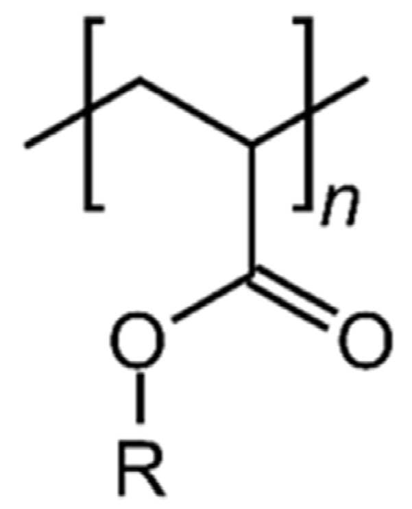
상기 화학식 1에서 n은 임의의 자연수이며 R은 수소, 알킬기, 알케닐기, 알카닐기 중 하나일 수 있다. In Formula 1, n is any natural number, and R may be one of hydrogen, an alkyl group, an alkenyl group, and an alkanyl group.
상기 제1 가교제와 상기 제2 가교제는 서로 같거나 다를 수 있다. 상기 제1 가교제와 상기 제2 가교제는 예를 들면 시안산염(cyanate) 계열일 수 있다. 상기 제1 가교제와 상기 제2 가교제는 각각 독립적으로 예를 들면 아래 화학식 2의 구조I과 구조II 중 하나를 가질 수 있다.The first cross-linking agent and the second cross-linking agent may be the same as or different from each other. The first cross-linking agent and the second cross-linking agent may be cyanate-based, for example. The first crosslinking agent and the second crosslinking agent may each independently have, for example, one of Structure I and Structure II of Formula 2 below.
<화학식 2><Formula 2>
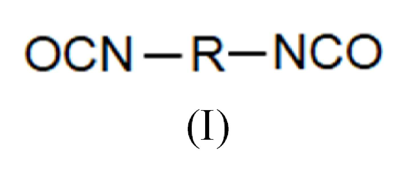
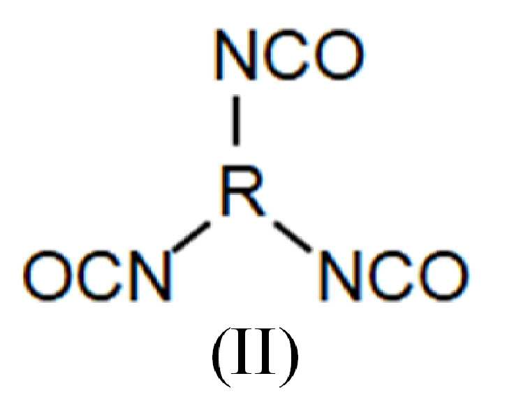
상기 화학식 2에서 R은 수소, 알킬기, 알케닐기, 알카닐기 중 하나일 수 있다. 상기 제1 가교제와 상기 제2 가교제의 함량에 따라 상기 캐리어 접착막(23)과 상기 디바이스 접착막(25)의 접착력이 조절될 수 있다. In Formula 2, R may be one of hydrogen, an alkyl group, an alkenyl group, and an alkanyl group. Adhesion between the
상기 제1 필러와 상기 제2 필러는 서로 같거나 다를 수 있다. 상기 제1 필러와 상기 제2 필러는 예를 들면, 실리칸, 알루미나, 세리아 또는 티타니아일 수 있다. 상기 제1 필러와 상기 제2 필러는 상기 상기 캐리어 접착막(23)과 상기 디바이스 접착막(25)의 modulus 또는 기계적 강도를 조절하기 위해 첨가될 수 있다.The first filler and the second filler may be the same as or different from each other. The first filler and the second filler may be, for example, silica, alumina, ceria, or titania. The first filler and the second filler may be added to adjust modulus or mechanical strength of the
상기 제1 이형제와 상기 제2 이형제는 서로 같거나 다를 수 있다. 상기 제1 이형제와 상기 제2 이형제는 예를 들면 실리콘 아크릴레이트일 수 있다. 상기 제1 이형제와 상기 제2 이형제는 예를 들면 아래 화학식 3의 구조를 가질 수 있다.The first release agent and the second release agent may be the same as or different from each other. The first release agent and the second release agent may be, for example, silicone acrylate. The first release agent and the second release agent may have structures represented by Chemical Formula 3 below, for example.
<화학식 3><Formula 3>
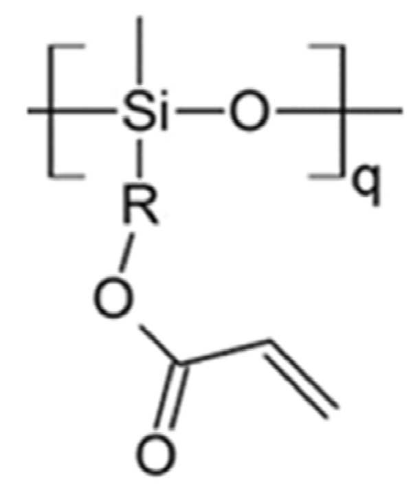
상기 화학식 3에서 q은 임의의 자연수이며 R은 알킬기, 알케닐기, 알카닐기 중 하나일 수 있다. 상기 화학식 3에서 실리콘이 결합된 부분은 소수성을 띄어 접착력을 약화시킬 수 있다. 상기 제1 이형제와 상기 제2 이형제는 상기 캐리어 접착막(23)과 상기 디바이스 접착막(25)의 접착력을 조절하기 위해 추가될 수 있다.In Formula 3, q is any natural number, and R may be one of an alkyl group, an alkenyl group, and an alkanyl group. In Chemical Formula 3, the portion to which silicone is bonded may be hydrophobic and thus may weaken adhesive strength. The first release agent and the second release agent may be added to adjust adhesive strength between the
상기 디바이스 접착막(25)은 가스 발포제를 더 포함할 수 있다. 반면에, 상기 캐리어 접착막(23)는 상기 가스 발포제를 배제할 수 있다. 상기 가스 발포제는 특정 파장의 빛에서 분해되어 질소 가스와, 반응성이 높은 라디칼을 형성하는 물질(또는 광개시제)일 수 있다. The
상기 가스 발포제는 바람직하게는 다이아지린(Diazirine)일 수 있다. 상기 다이아지린(Diazirine)은 아래의 화학반응식 (1)에서 개시된 바와 같이 예를 들면 350nm~400nm의 파장(W2)의 자외선에서 바람직하게는 약 355nm의 파장(W2)의 자외선에서 분해되어, 질소(N2) 가스와 카벤(Carbene) 라디칼을 형성할 수 있다. The gas blowing agent may preferably be diazirine. The diazirine is decomposed, for example, in ultraviolet light of a wavelength (W2) of about 350 nm to 400 nm, preferably in ultraviolet light of a wavelength (W2) of about 355 nm, as shown in chemical reaction formula (1) below, nitrogen ( It can form N 2 ) gas and carbene radical.
<화학 반응식1><Chemical Scheme 1>
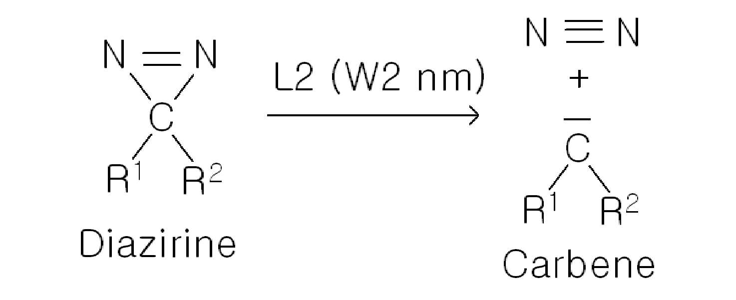
상기 화학반응식 1에서 상기 다이아지린의 R1과 R2는 각각 서로 독립적으로, 수소, 알킬기, 알케닐기, 알카닐기 중 하나일 수 있다.In Chemical Reaction Formula 1, R 1 and R 2 of diazirin may each independently represent one of hydrogen, an alkyl group, an alkenyl group, and an alkanyl group.
상기 캐리어 접착막(23)은 상기 제1 수지를 상기 캐리어 접착막(23)의 전체 중량의 80~99wt%으로 포함할 수 있다. 상기 캐리어 접착막(23)은 상기 제1 가교제를 상기 캐리어 접착막(23)의 전체 중량의 0.001~1wt%으로 포함할 수 있다. 상기 캐리어 접착막(23)은 상기 제1 필러를 상기 캐리어 접착막(23)의 전체 중량의 0.001~1wt%으로 포함할 수 있다. 상기 캐리어 접착막(23)은 상기 제1 이형제를 상기 캐리어 접착막(23)의 전체 중량의 0.001~1wt%으로 포함할 수 있다.The
상기 디바이스 접착막(25)은 상기 제2 수지를 상기 상기 디바이스 접착막(25)의 전체 중량의 80~99wt%으로 포함할 수 있다. 상기 디바이스 접착막(25)은 상기 제2 가교제를 상기 디바이스 접착막(25)의 전체 중량의 0.001~1wt%으로 포함할 수 있다. 상기 디바이스 접착막(25)은 상기 제2 필러를 상기 디바이스 접착막(25)의 전체 중량의 0.001~1wt%으로 포함할 수 있다. 상기 디바이스 접착막(25)은 상기 제2 이형제를 상기 디바이스 접착막(25)의 전체 중량의 0.001~1wt%으로 포함할 수 있다. 상기 디바이스 접착막(25)은 상기 가스 발포제를 상기 디바이스 접착막(25)의 전체 중량의 0.001~1wt%으로 포함할 수 있다.The
도 1, 도 2b 및 도 3b를 참조하면, 캐리어 기판(10)을 통해 제1 파장(W1)의 제1 빛(L1)을 조사하여 접착부재(20)를 1차 경화한다(제2 단게, S20). 상기 1차 경화에 의해 캐리어 기판(10)과 디바이스 기판(30) 사이에서 접착부재(20)의 접착력은 강화될 수 있다. Referring to FIGS. 1, 2B, and 3B, the
구체적으로, 접착 부재(20)가 개재되어 상기 캐리어 기판(10)과 디바이스 기판(30)이 본딩된 상태에서 상기 캐리어 기판(10)을 통해 상기 접착 부재(20)로 제1파장(W1)의 제1 빛(L1)을 조사한다. 제1파장(W1)은 바람직하게는 300nm~349nm이고 상기 제1 빛(L1)은 자외선일 수 있다. 이로써 상기 접착 부재(20)의 상기 캐리어 접착막(23)과 상기 디바이스 접착막(25) 내에서는 각각 상기 제1 빛(L1)에 의해 제1 가교제와 제2 가교제가 상기 제1 수지와 상기 제2 수지를 가교시키는 1차 경화 반응이 일어날 수 있다. 구체적으로 상기 1차 경화 반응에 의해 상기 캐리어 접착막(23) 내에서는 상기 제1 수지의 제1 고분자 사슬들(PB1)이 상기 제1 가교제의 제1 가교 그룹들(BC1)에 의해 연결될 수 있다. 또한 상기 1차 경화 반응에 의해 상기 디바이스 접착막(25) 내에서는 상기 제2 수지의 제2 고분자 사슬들(PB2)이 상기 제2 가교제의 제2 가교 그룹들(BC2)에 의해 연결될 수 있다. 상기 가스 발포제(GA)의 입자들은 입자들은 상기 디바이스 접착막(25) 내에서 제2 고분자 사슬들(PB2)과 제2 가교 그룹들(BC2) 사이에 분산되어 있을 수 있다. 상기 1차 경화 반응에 의해 상기 접착 부재(20)의 상기 캐리어 접착막(23)과 상기 디바이스 접착막(25)의 modulus는 증가할 수 있고, 상기 접착 부재(20)은 상기 디바이스 기판(30)을 상기 캐리어 기판(10)에 단단히 고정시킬 수 있다.Specifically, in a state in which the
도 1, 도 2b, 도 2c, 도 3a 및 도 3c를 참조하면, 디바이스 기판(30)에 대하여 백그라인딩 공정을 진행한다(제3 단계, S30). 구체적으로, 상기 디바이스 기판(30)의 제1 면(30a)가 위로 가도록 뒤집은 상태에서 백그라인딩 공정을 진행하여 상기 디바이스 기판(30)의 제 1 면(30a)에 인접한 부분을 소정 두께로 제거한다. 이로써 상기 기판부(30c)의 일부, 비아 절연막(31)의 일부, 및 확산 방지막(32)의 일부가 제거되고 상기 관통 비아(35)가 노출될 수 있다. 이때 상기 베벨 부분(ER)도 제거될 수 있다. 상기 기판부(30c)의 일부를 에치백하여 상기 절연막(31)의 측벽을 일부 노출시킬 수 있다. 1, 2b, 2c, 3a, and 3c, a back grinding process is performed on the device substrate 30 (third step, S30). Specifically, in a state where the
도 2d 및 도 3d를 참조하면, 상기 기판부(30c)의 뒷면에 제 2 패시베이션막(39)을 형성한다. 그리고 상기 관통 비아(35)와 접하는 제 2 도전 패드(41)를 형성한다. 도시하지는 않았지만 후속으로 상기 제 2 도전 패드(41)와 접하는 범프나 재배선 형성 공정을 진행할 수 있다. Referring to FIGS. 2D and 3D , a
이와 같이 상기 디바이스 기판(30)의 제 1 면(30a)에 대한 백 그라인딩 공정이나 패드 형성 공정 등을 진행한 후에 더 이상의 공정이 필요 없으면, 상기 디바이스 기판(30)을 상기 캐리어 기판(10)으로부터 분리한다. 이를 도 1, 도 e 및 도 2f를 참조하여 구체적으로 설명하기로 한다. In this way, if no further process is required after the back grinding process or the pad formation process for the
도 2e를 참조하면, 상기 캐리어 기판(10)이 부착된 상기 디바이스 기판(30)을 예를 들면, 칩 접착용 테이프(43) 상에 올려놓는다. 이때 상기 디바이스 기판(30)의 제 1 면(30a)이 상기 칩 접착용 테이프(43)와 닿도록 한다. Referring to FIG. 2E , the
도 1 및 도 2e를 참조하면, 상기 캐리어 기판(10)을 통해 제2 파장(W2)의 제2 빛(L2)을 조사하여 상기 접착 부재(20)를 2차 경화한다(제 4 단계, S40). 상기 2차 경화에 의해 디바이스 기판(30)과 상기 접착 부재(20) 간의 접착력을 약화될 수 있다. Referring to FIGS. 1 and 2E , the
구체적으로, 상기 캐리어 기판(10)을 통해 상기 접착 부재(20)로 제2 파장(W2)의 제2 빛(L2)을 조사한다. 상기 제2 파장(W2)은 도 2b의 제1 빛(L1)의 제1 파장(W1) 보다 클 수 있다. 바람직하게는 제2 파장(W2)은 350nm~400nm이고 상기 제2 빛(L2)은 자외선일 수 있다.Specifically, the second light L2 of the second wavelength W2 is radiated to the
도 2e, 도 3b 및 도 3e를 참조하면, 상기 디바이스 접착막(25)에 포함된 가스 발포제(GA)가 분해되어 질소(N2) 가스와 라디칼(RC)을 형성한다. 라디칼(RC)은 상기 디바이스 접착막(25) 내의 제2 고분자 사슬들(PB2)을 더 가교시켜 제2 고분자 사슬들(PB2)과 라디칼들(RC) 사이에 내부 결합(IC)이 형성된다. 이로써 상기 디바이스 접착막(25) 내에서 2차 경화 과정이 진행되고, Referring to FIGS. 2E, 3B, and 3E, the gas blowing agent (GA) included in the
이를 화학 반응식 2로 나타낼 수 있다.This can be represented by chemical reaction formula 2.
<화학 반응식 2><Chemical Scheme 2>

화학 반응식 2에서, 상기 가스 발포제인 다이아지린은 화학반응식 1,2에 개시된 바와 같이, 상기 제2 빛(L2)에 의해 질소(N2) 가스, 그리고 라디칼인 카벤(Carbene)으로 분해될 수 있다. 화학반응식 2의 

이로써 상기 디바이스 접착막(25)의 가교도/경화도는 더 증가할 수 있고, 이로써 상기 디바이스 접착막(25)의 modulus는 증가하며, 이는 상기 디바이스 접착막(25)과 상기 디바이스 기판(30) 간의 접착력의 감소를 초래한다. 또한 상기 질소 가스들은 상기 디바이스 접착막(25)과 상기 디바이스 기판(30) 사이에 공극들(AG)을 형성하여, 상기 디바이스 접착막(25)과 상기 디바이스 기판(30) 간의 접착력이 더욱 감소할 수 있다. 이로써 상기 접착 부재(20)와 상기 디바이스 기판(30) 간의 접착력이 더욱 감소할 수 있다.As a result, the degree of crosslinking/curing of the
반면에 캐리어 접착막(23)은 상기 가스 발포제(GA)를 포함하지 않으므로 상기 화학 반응식1,2이 발생하지 않는다. 따라서 상기 캐리어 접착막(23)은 상기 2차 경화 과정이 발생하지 않는다. 따라서 상기 캐리어 접착막(23)과 상기 캐리어 기판(10) 간의 접착력은 변함이 없다. On the other hand, since the
도 1 및 도 2f를 참조하면, 상기 접착 부재(20)와 상기 캐리어 기판(10)을 상기 디바이스 기판(30)으로부터 분리시킨다(제5 단계, S50). 이때 이미 위에서 설명한 바와 같이 상기 접착 부재(20)와 상기 디바이스 기판(30) 간의 접착력이 감소하였으므로, 상기 접착 부재(20)와 상기 캐리어 기판(10)이 상기 디바이스 기판(30)으로부터 용이하게 분리될 수 있다. 이로써 상기 디바이스 기판(30)의 크랙이 발생하지 않는다. Referring to FIGS. 1 and 2F , the
반도체 소자가 초소형화됨에 따라 상기 디바이스 기판(30)의 두께도 얇아지고 있으며 크랙에도 더욱 취약해질 수 있다. 그러나 본 발명에 따른 반도체 장치의 제조 방법을 이용하면, 상기 디바이스 기판(30)의 크랙, 가장자리 깨짐(chipping)이나 패시베이션막의 뜯김 등의 문제를 최소화/방지할 수 있다. 이로써 상기 디바이스 기판(30)이 깨지지 않아 수율을 향상시킬 수 있다. 또한 이로써 분리 공정 또는 Peel-off 공정의 속도를 향상시킬 수 있어 수율을 더욱 향상시킬 수 있다.As the semiconductor device is miniaturized, the thickness of the
후속으로 도 2g를 참조하면, 쏘잉(sawing) 공정을 진행하여 상기 스크라이브 레인 부분들(SR)을 절단하여 상기 칩 부분들(CR)을 분리한다. 그리고 도 2h를 참조하여, 패키지 기판(50) 상에 분리된 칩 부분(CR)을 예를 들면 플립 칩 본딩 방식으로 실장한다. 패키지 기판(50)은 인쇄회로 기판 또는 재배선 기판일 수 있다. 상기 칩 부분(CR)을 제 1 반도체 칩(CR)으로 명명하기로 한다. 상기 제 1 반도체 칩(CR) 상에 내부 솔더볼(47)을 이용하여 제 2 반도체 칩(54)을 플립 칩 본딩 방식으로 실장한다. 몰드 공정을 진행하여 상기 제 1 반도체 칩(CR)과 상기 제 2 반도체 칩(54)을 덮는 몰드막(58)을 형성한다. 그리고 상기 패키지 기판(50) 하부에 외부 솔더볼(52)을 부착시켜 반도체 패키지(100)를 형성한다. 도 2g에서는 하나의 제1 반도체 칩(CR)이 사용되었으나, 제1 반도체 칩(CR)은 복수개로 제공되어 패키지 기판(50)과 제 2 반도체 칩(54) 사이에 적층될 수도 있다. Subsequently, referring to FIG. 2G , a sawing process is performed to cut the scribe lane portions SR to separate the chip portions CR. And, referring to FIG. 2H , the separated chip portion CR is mounted on the
도 4는 본 발명의 실시예들에 따른 반도체 장치의 제조 방법을 나타내는 단면도이다. 4 is a cross-sectional view illustrating a method of manufacturing a semiconductor device according to example embodiments.
도 4를 참조하면, 접착 부재(20a)는 도 2a의 접착 부재(20)의 구조에서 제1 접착 보조막(27)과 제2 접착 보조막(29)을 더 포함할 수 있다. 상기 제1 접착 보조막(27)은 베이스 필름(21)과 캐리어 접착막(23) 사이에 개재되며, 베이스 필름(21)과 캐리어 접착막(23) 간의 접착력을 향상시킬 수 있다. 상기 제2 접착 보조막(29)은 베이스 필름(21)과 디바이스 접착막(25) 사이에 개재되며, 베이스 필름(21)과 디바이스 접착막(25) 간의 접착력을 향상시킬 수 있다. 상기 제1 접착 보조막(27)은 도 2a를 참조하여 설명한 제1 수지, 제1 가교제, 제1 필러를 포함할 수 있다. 상기 제1 접착 보조막(27)은 도 2a를 참조하여 설명한 제1 이형제와 가스 발포제를 배제할 수 있다. 상기 제2 접착 보조막(29)은 도 2a를 참조하여 설명한 제2 수지, 제2 가교제, 제2 필러를 포함할 수 있다. 상기 제2 접착 보조막(29)은 도 2a를 참조하여 설명한 제2 이형제와 가스 발포제를 배제할 수 있다. Referring to FIG. 4 , the
도 4와 같이 본딩한 후에 도 1, 도 2a~2h 및 도 3a~3e를 참조하여 설명한 바와 같이 공정들을 진행할 수 있다. 도 1의 1차 경화 단계(제2 단계, S20)에서 상기 제1 접착 보조막(27)과 상기 제2 접착 보조막(29)도 경화될 수 있다. 그러나, 도 1의 2차 경화 단계(제4 단계, S40)에서 상기 제1 접착 보조막(27)과 상기 제2 접착 보조막(29)는 추가로 경화되지 않으며, 접착력의 변화가 없을 수 있다. 그 외의 것들은 위에서 설명한 바와 동일/유사할 수 있다. After bonding as shown in FIG. 4, processes may be performed as described with reference to FIGS. 1, 2a to 2h, and 3a to 3e. In the first curing step (second step, S20) of FIG. 1, the first adhesive
도 5는 본 발명의 실시예들에 따른 반도체 장치의 제조 방법을 나타내는 단면도이다. 5 is a cross-sectional view illustrating a method of manufacturing a semiconductor device according to example embodiments.
도 5를 참조하면, 접착 부재(20b)는 도 2a의 접착 부재(20)의 구조에서 베이스 필름(21)을 배제할 수 있다. 상기 접착 부재(20b)는 차례로 적층된 디바이스 접착막(25)과 캐리어 접착막(23)을 포함할 수 있다. 이 경우, 도 1의 디바이스 기판(30) 상에 접착 부재(20b)를 개재하여 캐리어 기판을 본딩하는 단계(제1 단계, S10) 전에, 디바이스 기판(30) 상에 디바이스 접착막(25)과 캐리어 접착막(23)을 순차적으로 코팅하는 단계가 추가될 수 있다. 그리고, 도 1, 도 2a~2h 및 도 3a~3e를 참조하여 설명한 바와 같이 공정들을 진행할 수 있다. 그 외의 것들은 위에서 설명한 바와 동일/유사할 수 있다.Referring to FIG. 5 , the
도 6은 본 발명의 실시예들에 따른 반도체 장치의 제조 방법을 나타내는 단면도이다.6 is a cross-sectional view illustrating a method of manufacturing a semiconductor device according to example embodiments.
도 6을 참조하면, 접착 부재(20c)는 단층의 접착막으로 구성된다. 본 예에 따른 접착 부재(20c)는 도 2a의 접착 부재(20)의 구조에서 베이스 필름(21)과 캐리어 접착막(23)을 배제할 수 있다. 즉, 본 예에 따른 접착 부재(20c)는 도 2a를 참조하여 설명한 디바이스 접착막과 동일한 성분들과 조성을 가질 수 있다. 즉, 상기 접착 부재(20c)는 수지, 제2 가교제, 제2 필러, 제2 이형제 및 가스 발포제를 포함할 수 있다. 이 경우, 도 1의 디바이스 기판(30) 상에 접착 부재(20c)를 개재하여 캐리어 기판을 본딩하는 단계(제1 단계, S10) 전에, 디바이스 기판(30) 상에 접착 부재(20c)을 코팅하는 단계가 추가될 수 있다. 그리고, 도 1, 도 2a~2h 및 도 3a~3e를 참조하여 설명한 바와 같이 공정들을 진행할 수 있다. 접착 부재(20c)는 디바이스 기판(30)과 캐리어 기판(10) 사이에 개재되어 이들과 바로 접할 수 있다. 본 예에 있어서, 제2 단계(S20)에 의해 접착 부재(20c)는 1차 경화되고, 후에 백그라인딩 공정(제3 단계, S30) 및 패드 형성 공정 등을 진행한 후에 제4 단계(S40)에서 상기 접착 부재(20c)는 2차 경화되어 접착력이 약화되고 이로써 디바이스 기판(30)으로부터 크랙을 유발하지 않고 분리될 수 있다(제5 단계, S50). 그 외의 것들은 위에서 설명한 바와 동일/유사할 수 있다.Referring to FIG. 6 , the
도 7은 본 발명의 실시예들에 따라 도 2b의 ‘P2’ 부분을 확대한 도면이다.7 is an enlarged view of a 'P2' portion of FIG. 2B according to embodiments of the present invention.
도 7을 참조하면, 베이스 필름(21)은 탄성(Young's modulus), 단단함(toughness), 신장력(elongation)이 서로 다른 다층의 막들로 구성될 수 있다. 구체적인 일 예로써, 접착 부재(20d)의 베이스 필름(21)은 차례로 적층된 제1 내지 제3 베이스 필름들(21a, 21b, 21c)을 포함할 수 있다. 상기 제1 내지 제3 베이스 필름들(21a, 21b, 21c) 각각의 탄성, 단단함, 신장력이 서로 다를 수 있다. 이로써 보다 안정적으로 WSS 공정을 진행할 수 있다. 그 외의 구성 및 방법은 위에서 설명한 바와 동일/유사할 수 있다.Referring to FIG. 7 , the
이상, 첨부된 도면을 참조하여 본 발명의 실시예를 설명하였지만, 본 발명이 속하는 기술분야에서 통상의 지식을 가진 자는 본 발명이 그 기술적 사상이나 필수적인 특징을 변경하지 않고서 다른 구체적인 형태로 실시될 수 있다는 것을 이해할 수 있을 것이다. 그러므로 이상에서 기술한 실시예에는 모든 면에서 예시적인 것이며 한정적이 아닌 것으로 이해해야만 한다.Although the embodiments of the present invention have been described with reference to the accompanying drawings, those skilled in the art can implement the present invention in other specific forms without changing its technical spirit or essential features. You will understand that there is Therefore, it should be understood that the embodiments described above are illustrative in all respects and not restrictive.
Claims (20)
상기 접착 부재는:
베이스 필름;
상기 베이스 필름의 하부면 상에 배치되며 상기 디바이스 기판과 접하는 디바이스 접착막; 및
상기 베이스 필름의 상부면 상에 배치되며 상기 캐리어 기판과 접하는 캐리어 접착막을 포함하며,
상기 디바이스 접착막은 가스 발포제를 포함하고,
상기 캐리어 접착막은 상기 가스 발포제를 배제하는 반도체 장치의 제조 방법.
Bonding the carrier substrate on the device substrate using an adhesive member,
The adhesive member is:
base film;
a device adhesive film disposed on a lower surface of the base film and in contact with the device substrate; and
A carrier adhesive film disposed on an upper surface of the base film and in contact with the carrier substrate,
The device adhesive film includes a gas blowing agent,
The method of manufacturing a semiconductor device in which the carrier adhesive film excludes the gas blowing agent.
상기 캐리어 기판을 통해 제1 파장의 제1 자외선을 조사하여 상기 디바이스 접착막과 상기 캐리어 접착막을 각각 1차 경화시키는 단계;
상기 디바이스 기판에 대하여 백그라인딩 공정을 진행하여 상기 디바이스 기판의 두께를 줄이는 단계;
상기 캐리어 기판을 통해 상기 제1 파장과 다른 제2 파장의 제2 자외선을 조사하여 상기 디바이스 접착막을 2차 경화시키는 동시에 상기 디바이스 접착막과 상기 캐리어 기판 사이에 공극들을 형성하는 단계; 및
상기 디바이스 기판으로부터 상기 캐리어 기판과 상기 접착부재를 분리시키는 단계를 더 포함하는 반도체 장치의 제조 방법.
According to claim 1,
primary curing of the device adhesive layer and the carrier adhesive layer by irradiating a first ultraviolet ray of a first wavelength through the carrier substrate;
reducing the thickness of the device substrate by performing a back grinding process on the device substrate;
irradiating a second ultraviolet ray of a second wavelength different from the first wavelength through the carrier substrate to secondaryly cure the device adhesive film and simultaneously forming air gaps between the device adhesive film and the carrier substrate; and
The method of manufacturing a semiconductor device further comprising separating the carrier substrate and the adhesive member from the device substrate.
상기 디바이스 기판은 관통 비아를 포함하고,
상기 백 그라인딩 공정은 상기 관통 비아를 노출시키고,
상기 방법은 제2 자외선을 조사하는 단계 전에, 상기 디바이스 기판 상에 상기 관통 비아와 접하는 도전 패드를 형성하는 단계를 더 포함하는 반도체 장치의 제조 방법.
According to claim 2,
The device substrate includes a through via,
The back grinding process exposes the through vias;
The method of claim 1 , further comprising forming a conductive pad in contact with the through-via on the device substrate before irradiating the second ultraviolet ray.
상기 제2 파장은 상기 제1 파장보다 큰 반도체 장치의 제조 방법.
According to claim 2,
The second wavelength is greater than the first wavelength.
상기 제1 파장은 300nm~349nm이고,
상기 제2 파장은 350nm~400nm인 반도체 장치의 제조 방법.
According to claim 4,
The first wavelength is 300 nm to 349 nm,
The method of manufacturing a semiconductor device in which the second wavelength is 350 nm to 400 nm.
상기 제2 자외선에 의해 상기 가스 발포제는 분해되어 라디칼들과 질소 가스들을 형성하고,
상기 질소 가스들은 모여 상기 공극들을 형성하고,
상기 라디칼들은 상기 디바이스 접착막을 2차 경화시키는 반도체 장치의 제조 방법.
According to claim 2,
The gas blowing agent is decomposed by the second ultraviolet rays to form radicals and nitrogen gas;
The nitrogen gases gather to form the pores,
The radicals are a method of manufacturing a semiconductor device for secondary curing the device adhesive film.
상기 가스 발포제는 다이아지린(Diazirine)이고,
상기 라디칼들은 카벤(Carbene)인 반도체 장치의 제조 방법.
According to claim 6,
The gas blowing agent is Diazirine,
The method of manufacturing a semiconductor device in which the radicals are carbene.
상기 가스 발포제는 다이아지린(Diazirine)인 반도체 장치의 제조 방법.
According to claim 1,
The method of manufacturing a semiconductor device in which the gas blowing agent is diazirine.
상기 캐리어 접착막은 제1 수지, 제1 가교제, 제1 필러 및 제1 이형제를 포함하고,
상기 디바이스 접착막은 상기 제2 수지, 상기 제2 가교제, 상기 제2 필러 및 상기 제2 이형제를 더 포함하는 반도체 장치의 제조 방법.
According to claim 1,
The carrier adhesive film includes a first resin, a first crosslinking agent, a first filler, and a first release agent,
The device adhesive film further comprises the second resin, the second crosslinking agent, the second filler, and the second release agent.
상기 접착 부재는:
상기 캐리어 기판과 상기 캐리어 접착막 사이에 개재되는 제1 접착 보조막; 및
상기 디바이스 기판과 상기 디바이스 기판 사이에 개재되는 제2 접착 보조막을 더 포함하되,
상기 제1 접착 보조막은 상기 제1 수지, 상기 제1 가교제, 및 상기 제1 필러를 포함하되 상기 제1 이형제를 배제하고,
상기 제2 접착 보조막은 상기 제2 수지, 상기 제2 가교제, 및 상기 제2 필러를 포함하되 상기 제2 이형제를 배제하는 반도체 장치의 제조 방법.
According to claim 9,
The adhesive member is:
a first adhesion auxiliary film interposed between the carrier substrate and the carrier adhesive film; and
Further comprising a second adhesion auxiliary film interposed between the device substrate and the device substrate,
The first adhesive auxiliary film includes the first resin, the first crosslinking agent, and the first filler but excludes the first release agent,
The second adhesion auxiliary film includes the second resin, the second crosslinking agent, and the second filler, but excludes the second release agent.
상기 캐리어 기판을 통해 제1 파장의 제1 빛을 조사하여 상기 접착 부재를 1차 경화시키는 단계;
상기 디바이스 기판에 대하여 백그라인딩 공정을 진행하여 상기 디바이스 기판의 두께를 줄이는 단계;
상기 캐리어 기판을 통해 상기 제1 파장과 다른 제2 파장의 제2 빛을 조사하여 상기 접착 부재를 2차 경화시키는 동시에 상기 접착 부재와 상기 캐리어 기판 사이에 공극들을 형성하는 단계; 및
상기 디바이스 기판으로부터 상기 캐리어 기판과 상기 접착부재를 분리시키는 단계를 포함하는 반도체 장치의 제조 방법.
bonding the carrier substrate on the device substrate with an adhesive member interposed therebetween;
primary curing of the adhesive member by irradiating a first light of a first wavelength through the carrier substrate;
reducing the thickness of the device substrate by performing a back grinding process on the device substrate;
irradiating a second light of a second wavelength different from the first wavelength through the carrier substrate to secondaryly cure the adhesive member and simultaneously forming air gaps between the adhesive member and the carrier substrate; and
and separating the carrier substrate and the adhesive member from the device substrate.
상기 접착 부재는:
베이스 필름;
상기 베이스 필름의 하부면 상에 배치되며 상기 디바이스 기판과 접하는 디바이스 접착막; 및
상기 베이스 필름의 상부면 상에 배치되며 상기 캐리어 기판과 접하는 캐리어 접착막을 포함하며,
상기 디바이스 접착막은 가스 발포제를 포함하고,
상기 캐리어 접착막은 상기 가스 발포제를 배제하는 반도체 장치의 제조 방법.
According to claim 11,
The adhesive member is:
base film;
a device adhesive film disposed on a lower surface of the base film and in contact with the device substrate; and
A carrier adhesive film disposed on an upper surface of the base film and in contact with the carrier substrate,
The device adhesive film includes a gas blowing agent,
The method of manufacturing a semiconductor device in which the carrier adhesive film excludes the gas blowing agent.
상기 디바이스 기판은 관통 비아를 포함하고,
상기 백 그라인딩 공정은 상기 관통 비아를 노출시키고,
상기 방법은 제2 빛을 조사하는 단계 전에, 상기 디바이스 기판 상에 상기 관통 비아와 접하는 도전 패드를 형성하는 단계를 더 포함하는 반도체 장치의 제조 방법.
According to claim 11,
The device substrate includes a through via,
The back grinding process exposes the through vias;
The method of claim 1 , further comprising forming a conductive pad on the device substrate that contacts the through-via before irradiating a second light.
상기 제1 파장은 300nm~349nm이고,
상기 제2 파장은 350nm~400nm인 반도체 장치의 제조 방법.
According to claim 11,
The first wavelength is 300 nm to 349 nm,
The method of manufacturing a semiconductor device in which the second wavelength is 350 nm to 400 nm.
상기 접착 부재는 가스 발포제를 포함하고,
상기 제2 빛에 의해 상기 가스 발포제는 분해되어 라디칼들과 질소 가스들을 형성하고,
상기 질소 가스들은 모여 상기 공극들을 형성하고,
상기 라디칼들은 상기 접착 부재를 2차 경화시키는 반도체 장치의 제조 방법.
According to claim 11,
The adhesive member includes a gas blowing agent,
The gas blowing agent is decomposed by the second light to form radicals and nitrogen gas;
The nitrogen gases gather to form the pores,
The radicals secondarily cure the adhesive member.
상기 가스 발포제는 다이아지린(Diazirine)이고,
상기 라디칼들은 카벤(Carbene)인 반도체 장치의 제조 방법.
According to claim 15,
The gas blowing agent is Diazirine,
The method of manufacturing a semiconductor device in which the radicals are carbene.
상기 캐리어 기판을 통해 제1 파장의 제1 자외선을 조사하여 상기 접착 부재를 1차 경화시키는 단계;
상기 디바이스 기판에 대하여 백그라인딩 공정을 진행하여 상기 디바이스 기판의 두께를 줄이는 단계;
상기 캐리어 기판을 통해 상기 제1 파장과 다른 제2 파장의 제2 자외선을 조사하여 상기 접착 부재를 2차 경화시키는 동시에 상기 접착 부재와 상기 캐리어 기판 사이에 공극들을 형성하는 단계; 및
상기 디바이스 기판으로부터 상기 캐리어 기판과 상기 접착부재를 분리시키는 단계를 포함하되,
상기 접착 부재는:
베이스 필름;
상기 베이스 필름의 하부면 상에 배치되며 상기 디바이스 기판과 접하는 디바이스 접착막; 및
상기 베이스 필름의 상부면 상에 배치되며 상기 캐리어 기판과 접하는 캐리어 접착막을 포함하며,
상기 디바이스 접착막은 가스 발포제를 포함하고,
상기 캐리어 접착막은 상기 가스 발포제를 배제하는 반도체 장치의 제조 방법.
Bonding the carrier substrate on the device substrate using an adhesive member;
primary curing of the adhesive member by irradiating a first ultraviolet ray of a first wavelength through the carrier substrate;
reducing the thickness of the device substrate by performing a back grinding process on the device substrate;
irradiating a second ultraviolet ray of a second wavelength different from the first wavelength through the carrier substrate to secondaryly cure the adhesive member and simultaneously forming air gaps between the adhesive member and the carrier substrate; and
Including the step of separating the carrier substrate and the adhesive member from the device substrate,
The adhesive member is:
base film;
a device adhesive film disposed on a lower surface of the base film and in contact with the device substrate; and
A carrier adhesive film disposed on an upper surface of the base film and in contact with the carrier substrate,
The device adhesive film includes a gas blowing agent,
The method of manufacturing a semiconductor device in which the carrier adhesive film excludes the gas blowing agent.
상기 제1 파장은 300nm~349nm이고,
상기 제2 파장은 350nm~400nm인 반도체 장치의 제조 방법.
18. The method of claim 17,
The first wavelength is 300 nm to 349 nm,
The method of manufacturing a semiconductor device in which the second wavelength is 350 nm to 400 nm.
상기 가스 발포제는 다이아지린(Diazirine)이고,
상기 라디칼들은 카벤(Carbene)인 반도체 장치의 제조 방법.
According to claim 17,
The gas blowing agent is Diazirine,
The method of manufacturing a semiconductor device in which the radicals are carbene.
상기 캐리어 접착막은 제1 수지, 제1 가교제, 제1 필러 및 제1 이형제를 포함하고,
상기 캐리어 접착막은 제2 수지, 제2 가교제, 제2 필러 및 제2 이형제를 더 포함하는 반도체 장치의 제조 방법.
According to claim 17,
The carrier adhesive film includes a first resin, a first crosslinking agent, a first filler, and a first release agent,
The method of claim 1 , wherein the carrier adhesive film further comprises a second resin, a second crosslinking agent, a second filler, and a second release agent.
Priority Applications (3)
| Application Number | Priority Date | Filing Date | Title |
|---|---|---|---|
| KR1020210117324A KR20230034506A (en) | 2021-09-03 | 2021-09-03 | Method of fabricating a semiconductor device using gas blowing agent |
| CN202210676861.6A CN115763297A (en) | 2021-09-03 | 2022-06-14 | Method for manufacturing semiconductor device using gas foaming agent |
| US17/861,490 US12521977B2 (en) | 2021-09-03 | 2022-07-11 | Method of manufacturing semiconductor device using gas blowing agent |
Applications Claiming Priority (1)
| Application Number | Priority Date | Filing Date | Title |
|---|---|---|---|
| KR1020210117324A KR20230034506A (en) | 2021-09-03 | 2021-09-03 | Method of fabricating a semiconductor device using gas blowing agent |
Publications (1)
| Publication Number | Publication Date |
|---|---|
| KR20230034506A true KR20230034506A (en) | 2023-03-10 |
Family
ID=85349986
Family Applications (1)
| Application Number | Title | Priority Date | Filing Date |
|---|---|---|---|
| KR1020210117324A Pending KR20230034506A (en) | 2021-09-03 | 2021-09-03 | Method of fabricating a semiconductor device using gas blowing agent |
Country Status (3)
| Country | Link |
|---|---|
| US (1) | US12521977B2 (en) |
| KR (1) | KR20230034506A (en) |
| CN (1) | CN115763297A (en) |
Families Citing this family (1)
| Publication number | Priority date | Publication date | Assignee | Title |
|---|---|---|---|---|
| KR20220169043A (en) * | 2021-06-17 | 2022-12-27 | 삼성전자주식회사 | Semiconductor package and method of fabricating the same |
Family Cites Families (10)
| Publication number | Priority date | Publication date | Assignee | Title |
|---|---|---|---|---|
| JP2004296839A (en) | 2003-03-27 | 2004-10-21 | Kansai Paint Co Ltd | Method for manufacturing semiconductor chip |
| KR100885099B1 (en) | 2003-12-15 | 2009-02-20 | 후루카와 덴키 고교 가부시키가이샤 | Wafer processing tape and its manufacturing method |
| US8791549B2 (en) * | 2009-09-22 | 2014-07-29 | Taiwan Semiconductor Manufacturing Company, Ltd. | Wafer backside interconnect structure connected to TSVs |
| JP2013185014A (en) * | 2012-03-06 | 2013-09-19 | Sekisui Chem Co Ltd | Adhesive composition, adhesive tape, method for processing semiconductor wafer and method for producing tsv wafer |
| KR101276487B1 (en) | 2012-10-05 | 2013-06-18 | 주식회사 이녹스 | Wafer laminated body and method for bonding and debonding between device wafer and carrier wafer |
| US20140144593A1 (en) | 2012-11-28 | 2014-05-29 | International Business Machiness Corporation | Wafer debonding using long-wavelength infrared radiation ablation |
| KR20160067517A (en) | 2014-12-04 | 2016-06-14 | 삼성전자주식회사 | method of manufacturing semiconductor devices |
| US20190194506A1 (en) | 2017-12-22 | 2019-06-27 | International Business Machines Corporation | Low temperature adhesive bond material |
| CN111565768B (en) | 2018-02-20 | 2022-09-02 | 泰尔茂株式会社 | Medical instrument |
| US10580700B1 (en) | 2019-02-15 | 2020-03-03 | Mikro Mesa Technology Co., Ltd. | Method for avoiding crack formation during laser lift-off process |
-
2021
- 2021-09-03 KR KR1020210117324A patent/KR20230034506A/en active Pending
-
2022
- 2022-06-14 CN CN202210676861.6A patent/CN115763297A/en active Pending
- 2022-07-11 US US17/861,490 patent/US12521977B2/en active Active
Also Published As
| Publication number | Publication date |
|---|---|
| CN115763297A (en) | 2023-03-07 |
| US20230087718A1 (en) | 2023-03-23 |
| US12521977B2 (en) | 2026-01-13 |
Similar Documents
| Publication | Publication Date | Title |
|---|---|---|
| CN101552248B (en) | A semiconductor device and a manufacturing method thereof | |
| US8076756B2 (en) | Structure for inhibiting back end of line damage from dicing and chip packaging interaction failures | |
| US10734357B2 (en) | Chip package structure with molding layer | |
| TWI614850B (en) | Semiconductor package structure and method of forming same | |
| TWI626717B (en) | Semiconductor package structure | |
| US8981558B2 (en) | Semiconductor device | |
| US20120248605A1 (en) | Semiconductor device and manufacturing method thereof | |
| JP4596001B2 (en) | Manufacturing method of semiconductor device | |
| JP2009049410A (en) | Semiconductor chip package, method for manufacturing the same, and electronic device including the same | |
| CN1499590A (en) | Semiconductor device and manufacturing method thereof | |
| CN1645565A (en) | Semiconductor device and manufacturing method thereof | |
| CN102148203A (en) | Semiconductor chip and method of forming conductor pillar | |
| KR20200031202A (en) | A redistribution substrate, a method for manufacturing the same, and a semiconductor package including the same | |
| US12261164B2 (en) | Semiconductor package | |
| KR20210145568A (en) | Semiconductor devices including stacked substrates and method for fabricating the same | |
| KR20230034506A (en) | Method of fabricating a semiconductor device using gas blowing agent | |
| CN101673708A (en) | Semiconductor device having an interlayer insulating film wiring laminated structure section and method of fabricating the same | |
| CN113937050A (en) | Treatment belt | |
| US20250336827A1 (en) | Semiconductor package and method of fabricating the same | |
| TWI902884B (en) | Semiconductor package | |
| US20120061830A1 (en) | Back side protective structure for a semiconductor package | |
| US20240194553A1 (en) | Semiconductor package and method for manufacturing the same | |
| US20250029955A1 (en) | Semiconductor package having an inorganic layer on a mold layer and method of fabricating the same | |
| US20240290754A1 (en) | Semiconductor package | |
| KR20250017085A (en) | Semiconductor package and method of fabricating the same |
Legal Events
| Date | Code | Title | Description |
|---|---|---|---|
| PA0109 | Patent application |
St.27 status event code: A-0-1-A10-A12-nap-PA0109 |
|
| PG1501 | Laying open of application |
St.27 status event code: A-1-1-Q10-Q12-nap-PG1501 |
|
| A201 | Request for examination | ||
| P11-X000 | Amendment of application requested |
St.27 status event code: A-2-2-P10-P11-nap-X000 |
|
| P13-X000 | Application amended |
St.27 status event code: A-2-2-P10-P13-nap-X000 |
|
| PA0201 | Request for examination |
St.27 status event code: A-1-2-D10-D11-exm-PA0201 |
|
| D13-X000 | Search requested |
St.27 status event code: A-1-2-D10-D13-srh-X000 |
|
| D21 | Rejection of application intended |
Free format text: ST27 STATUS EVENT CODE: A-1-2-D10-D21-EXM-PE0902 (AS PROVIDED BY THE NATIONAL OFFICE) |
|
| PE0902 | Notice of grounds for rejection |
St.27 status event code: A-1-2-D10-D21-exm-PE0902 |
|
| P11 | Amendment of application requested |
Free format text: ST27 STATUS EVENT CODE: A-2-2-P10-P11-NAP-X000 (AS PROVIDED BY THE NATIONAL OFFICE) |
|
| P11-X000 | Amendment of application requested |
St.27 status event code: A-2-2-P10-P11-nap-X000 |
|
| P22-X000 | Classification modified |
St.27 status event code: A-2-2-P10-P22-nap-X000 |