KR20220110517A - Variable Electrode Size Area Arrays on Thin Film Transistor-Based Digital Microfluidic Devices for Precise Droplet Manipulation - Google Patents
Variable Electrode Size Area Arrays on Thin Film Transistor-Based Digital Microfluidic Devices for Precise Droplet Manipulation Download PDFInfo
- Publication number
- KR20220110517A KR20220110517A KR1020227022145A KR20227022145A KR20220110517A KR 20220110517 A KR20220110517 A KR 20220110517A KR 1020227022145 A KR1020227022145 A KR 1020227022145A KR 20227022145 A KR20227022145 A KR 20227022145A KR 20220110517 A KR20220110517 A KR 20220110517A
- Authority
- KR
- South Korea
- Prior art keywords
- electrodes
- thin film
- density
- source lines
- digital microfluidic
- Prior art date
- Legal status (The legal status is an assumption and is not a legal conclusion. Google has not performed a legal analysis and makes no representation as to the accuracy of the status listed.)
- Withdrawn
Links
Images


Classifications
-
- B—PERFORMING OPERATIONS; TRANSPORTING
- B01—PHYSICAL OR CHEMICAL PROCESSES OR APPARATUS IN GENERAL
- B01L—CHEMICAL OR PHYSICAL LABORATORY APPARATUS FOR GENERAL USE
- B01L3/00—Containers or dishes for laboratory use, e.g. laboratory glassware; Droppers
- B01L3/50—Containers for the purpose of retaining a material to be analysed, e.g. test tubes
- B01L3/502—Containers for the purpose of retaining a material to be analysed, e.g. test tubes with fluid transport, e.g. in multi-compartment structures
- B01L3/5027—Containers for the purpose of retaining a material to be analysed, e.g. test tubes with fluid transport, e.g. in multi-compartment structures by integrated microfluidic structures, i.e. dimensions of channels and chambers are such that surface tension forces are important, e.g. lab-on-a-chip
- B01L3/502769—Containers for the purpose of retaining a material to be analysed, e.g. test tubes with fluid transport, e.g. in multi-compartment structures by integrated microfluidic structures, i.e. dimensions of channels and chambers are such that surface tension forces are important, e.g. lab-on-a-chip characterised by multiphase flow arrangements
- B01L3/502784—Containers for the purpose of retaining a material to be analysed, e.g. test tubes with fluid transport, e.g. in multi-compartment structures by integrated microfluidic structures, i.e. dimensions of channels and chambers are such that surface tension forces are important, e.g. lab-on-a-chip characterised by multiphase flow arrangements specially adapted for droplet or plug flow, e.g. digital microfluidics
- B01L3/502792—Containers for the purpose of retaining a material to be analysed, e.g. test tubes with fluid transport, e.g. in multi-compartment structures by integrated microfluidic structures, i.e. dimensions of channels and chambers are such that surface tension forces are important, e.g. lab-on-a-chip characterised by multiphase flow arrangements specially adapted for droplet or plug flow, e.g. digital microfluidics for moving individual droplets on a plate, e.g. by locally altering surface tension
-
- B—PERFORMING OPERATIONS; TRANSPORTING
- B01—PHYSICAL OR CHEMICAL PROCESSES OR APPARATUS IN GENERAL
- B01L—CHEMICAL OR PHYSICAL LABORATORY APPARATUS FOR GENERAL USE
- B01L3/00—Containers or dishes for laboratory use, e.g. laboratory glassware; Droppers
- B01L3/50—Containers for the purpose of retaining a material to be analysed, e.g. test tubes
- B01L3/502—Containers for the purpose of retaining a material to be analysed, e.g. test tubes with fluid transport, e.g. in multi-compartment structures
- B01L3/5027—Containers for the purpose of retaining a material to be analysed, e.g. test tubes with fluid transport, e.g. in multi-compartment structures by integrated microfluidic structures, i.e. dimensions of channels and chambers are such that surface tension forces are important, e.g. lab-on-a-chip
- B01L3/502769—Containers for the purpose of retaining a material to be analysed, e.g. test tubes with fluid transport, e.g. in multi-compartment structures by integrated microfluidic structures, i.e. dimensions of channels and chambers are such that surface tension forces are important, e.g. lab-on-a-chip characterised by multiphase flow arrangements
- B01L3/502784—Containers for the purpose of retaining a material to be analysed, e.g. test tubes with fluid transport, e.g. in multi-compartment structures by integrated microfluidic structures, i.e. dimensions of channels and chambers are such that surface tension forces are important, e.g. lab-on-a-chip characterised by multiphase flow arrangements specially adapted for droplet or plug flow, e.g. digital microfluidics
-
- B—PERFORMING OPERATIONS; TRANSPORTING
- B01—PHYSICAL OR CHEMICAL PROCESSES OR APPARATUS IN GENERAL
- B01L—CHEMICAL OR PHYSICAL LABORATORY APPARATUS FOR GENERAL USE
- B01L2200/00—Solutions for specific problems relating to chemical or physical laboratory apparatus
- B01L2200/02—Adapting objects or devices to another
- B01L2200/023—Adapting objects or devices to another adapted for different sizes of tubes, tips or container
-
- B—PERFORMING OPERATIONS; TRANSPORTING
- B01—PHYSICAL OR CHEMICAL PROCESSES OR APPARATUS IN GENERAL
- B01L—CHEMICAL OR PHYSICAL LABORATORY APPARATUS FOR GENERAL USE
- B01L2200/00—Solutions for specific problems relating to chemical or physical laboratory apparatus
- B01L2200/12—Specific details about manufacturing devices
-
- B—PERFORMING OPERATIONS; TRANSPORTING
- B01—PHYSICAL OR CHEMICAL PROCESSES OR APPARATUS IN GENERAL
- B01L—CHEMICAL OR PHYSICAL LABORATORY APPARATUS FOR GENERAL USE
- B01L2300/00—Additional constructional details
- B01L2300/06—Auxiliary integrated devices, integrated components
- B01L2300/0627—Sensor or part of a sensor is integrated
- B01L2300/0645—Electrodes
-
- B—PERFORMING OPERATIONS; TRANSPORTING
- B01—PHYSICAL OR CHEMICAL PROCESSES OR APPARATUS IN GENERAL
- B01L—CHEMICAL OR PHYSICAL LABORATORY APPARATUS FOR GENERAL USE
- B01L2300/00—Additional constructional details
- B01L2300/08—Geometry, shape and general structure
- B01L2300/0887—Laminated structure
-
- B—PERFORMING OPERATIONS; TRANSPORTING
- B01—PHYSICAL OR CHEMICAL PROCESSES OR APPARATUS IN GENERAL
- B01L—CHEMICAL OR PHYSICAL LABORATORY APPARATUS FOR GENERAL USE
- B01L2300/00—Additional constructional details
- B01L2300/16—Surface properties and coatings
- B01L2300/161—Control and use of surface tension forces, e.g. hydrophobic, hydrophilic
-
- B—PERFORMING OPERATIONS; TRANSPORTING
- B01—PHYSICAL OR CHEMICAL PROCESSES OR APPARATUS IN GENERAL
- B01L—CHEMICAL OR PHYSICAL LABORATORY APPARATUS FOR GENERAL USE
- B01L2400/00—Moving or stopping fluids
- B01L2400/04—Moving fluids with specific forces or mechanical means
- B01L2400/0403—Moving fluids with specific forces or mechanical means specific forces
- B01L2400/0415—Moving fluids with specific forces or mechanical means specific forces electrical forces, e.g. electrokinetic
- B01L2400/0427—Electrowetting
Landscapes
- Chemical & Material Sciences (AREA)
- Dispersion Chemistry (AREA)
- Health & Medical Sciences (AREA)
- Analytical Chemistry (AREA)
- General Health & Medical Sciences (AREA)
- Hematology (AREA)
- Clinical Laboratory Science (AREA)
- Chemical Kinetics & Catalysis (AREA)
- Physical Or Chemical Processes And Apparatus (AREA)
- Automatic Analysis And Handling Materials Therefor (AREA)
Abstract
디지털 미세유체 디바이스는 기판 및 제어기를 포함한다. 기판은 제 1 고해상도 영역 및 제 2 저해상도 영역, 그리고 소수성 층을 포함한다. 제 1 영역은, 제 1 밀도 (D1) 를 갖는 제 1 복수의 전극들, 및 제 1 복수의 전극들에 커플링된 박막 트랜지스터들의 제 1 세트를 포함한다. 제 2 영역은, 제 2 밀도 (D2) 를 갖는 제 2 복수의 전극들 (여기서, D2 < D1), 및 제 2 복수의 전극들에 커플링된 박막 트랜지스터들의 제 2 세트를 포함한다.A digital microfluidic device includes a substrate and a controller. The substrate includes a first high resolution region and a second low resolution region, and a hydrophobic layer. The first region includes a first plurality of electrodes having a first density D1 and a first set of thin film transistors coupled to the first plurality of electrodes. The second region includes a second plurality of electrodes having a second density D2, where D2 < D1, and a second set of thin film transistors coupled to the second plurality of electrodes.

Description
관련 출원들Related applications
본 출원은 2019년 12월 4일자로 출원된 미국 가특허출원 제62/943,295호를 우선권 주장한다. 본 명세서에서 개시된 모든 특허들 및 공보들은 전부 참조에 의해 통합된다.This application claims priority to U.S. Provisional Patent Application No. 62/943,295, filed on December 4, 2019. All patents and publications disclosed herein are incorporated by reference in their entirety.
디지털 미세유체 디바이스들은 독립적인 전극들을 사용하여 한정된 환경에서 액적들을 추진, 분리 및 결합함으로써, "랩-온-칩(lab-on-a-chip)" 을 제공한다. 디지털 미세유체 디바이스들은 대안적으로, 전기영동 플로우 및/또는 마이크로펌프들에 의존하는 경쟁하는 미세유체 시스템들로부터 그 방법을 더 구별하기 위해 유전체 상의 전기습윤 (electrowetting on dielectric) 또는 "EWoD" 로서 지칭된다. 전기습윤 기술의 2012 리뷰는 Wheeler 에 의해 "Digital Microfluidics," Annu. Rev. Anal. Chem. 2012, 5:413-40 에서 제공되었고, 이는 본 명세서에서 전부 참조에 의해 통합된다. 그 기법은 샘플 준비, 분석, 및 합성 케미스트리가 샘플들 및 시약들 양자 모두의 아주 적은 양으로 수행되게 한다. 최근에, 전기습윤을 사용하는 미세유체 셀들에서의 제어된 액적 조작은 상업적으로 실행가능하게 되었고; 이제, Oxford Nanopore 와 같은 큰 생명 과학 회사로부터 입수가능한 제품들이 있다.Digital microfluidic devices provide “lab-on-a-chip” by using independent electrodes to propel, separate, and combine droplets in a confined environment. Digital microfluidic devices are alternatively referred to as electrowetting on dielectric or “EWoD” to further distinguish their method from competing microfluidic systems that rely on electrophoretic flow and/or micropumps. do. A 2012 review of electrowetting techniques is by Wheeler in "Digital Microfluidics," Annu. Rev. Anal. Chem. 2012, 5:413-40, which is incorporated herein by reference in its entirety. The technique allows sample preparation, analysis, and synthetic chemistry to be performed with very small amounts of both samples and reagents. Recently, controlled droplet manipulation in microfluidic cells using electrowetting has become commercially viable; Now, there are products available from large life sciences companies such as Oxford Nanopore.
EWoD 에 대한 대부분의 문헌 보고서들은 소위 "직접 구동 (direct drive)" 디바이스들 (일명, "세그먼트화된" 디바이스들) 을 수반하며, 이에 의해, 10 내지 수백개의 전극들이 제어기로 직접 구동된다. 세그먼트화된 디바이스들은 제조가 용이하지만, 전극들의 수는 공간 및 구동 제약들에 의해 제한된다. 이에 따라, 직접 구동 디바이스들에서 대규모 병렬 분석들, 반응들 등을 수행하는 것이 가능하지 않다. 이에 비해, "액티브 매트릭스" 디바이스들 (일명, 액티브 매트릭스 EWoD, 일명, AM-EWoD) 디바이스들은 수천, 수십만 또는 심지어 수백만 개의 어드레스가능 전극들을 가질 수 있다. AM-EWoD 디바이스들에서, 전극들은 통상적으로, 박막 트랜지스터들 (TFT) 에 의해 스위칭되며 액적 모션은 프로그래밍가능하여, AM-EWoD 어레이들이 다중 액적들을 제어하고 동시 분석 프로세스들을 실행하기 위한 대자유를 허용하는 범용 디바이스들로서 사용될 수 있다.Most literature reports on EWoD involve so-called “direct drive” devices (aka “segmented” devices), whereby ten to hundreds of electrodes are driven directly into the controller. Segmented devices are easy to manufacture, but the number of electrodes is limited by space and drive constraints. Accordingly, it is not possible to perform massively parallel analyzes, reactions, etc. in direct drive devices. In contrast, “active matrix” devices (aka, active matrix EWoD, aka, AM-EWoD) devices may have thousands, hundreds of thousands or even millions of addressable electrodes. In AM-EWoD devices, electrodes are typically switched by thin film transistors (TFT) and droplet motion is programmable, allowing AM-EWoD arrays great freedom to control multiple droplets and execute simultaneous analysis processes. can be used as general-purpose devices.
액티브 매트릭스 디바이스들에 대해, 구동 신호들은 종종, 제어기로부터 게이트 및 스캔 구동기들로 출력되며, 이 구동기들은, 차례로, 액티브 매트릭스에서 다양한 TFT 를 활성화하기 위해 요구된 전류-전압 입력들을 제공한다. 하지만, 예컨대, 이미지 데이터를 수신하고, TFT들을 활성화하기 위해 필요한 전류-전압 입력들을 출력할 수 있는 제어기-구동기들이 상업적으로 입수가능하다. 예컨대, UltraChip 으로부터 입수가능한 다양한 제어기-구동기들 참조.For active matrix devices, drive signals are often output from a controller to gate and scan drivers, which in turn provide the required current-voltage inputs to activate the various TFTs in the active matrix. However, for example, controller-drivers capable of receiving image data and outputting the current-voltage inputs necessary to activate the TFTs are commercially available. See, for example, the various controller-actuators available from UltraChip.
AM-EWoD 디바이스의 모든 영역들에 대해 고 밀도의 전극들을 갖는 것은, 특히, 복잡한 기능들이 모든 위치들에서 실행되지 않는다면, 항상 필요한 것은 아니다. 모든 위치들에서 고 밀도 전극들을 갖는 것은 더 빠른 (및 더 비싼) 구동기를 요구하며, 또한, 요구되는 데이터 프로세싱의 양도 증가시킨다. 일부 경우들에 있어서, 일부 영역들에서는 더 큰 전극들을 갖고 다른 영역들에서는 더 작은 전극들을 갖는 것이 유리할 것이다. 통상적으로, 전극들의 그룹들 (즉, "집성된" 전극들) 이 기본 (더 작은) 전극 사이즈보다 더 큰 구조들을 나타내기 위해 사용되었다. 그럼에도 불구하고, 더 작은 전극들을 결합하여 더 큰 전극들을 나타내는 것은 증가된 수의 구동 라인들 및 데이터 요건들로 인해 시스템의 복잡도를 증가시킨다. 미국 특허출원 공개 제2016/0184823호는 이러한 문제에 대한 솔루션을 제안한다. 이는 8개의 상이한 사이즈들의 전극 서브어레이들를 개시하지만, '823 공개의 아키텍처는 구동 라인 및 지오메트리 요건들로 인해 동일한 TFT 플랫폼 상에 상이한 사이즈의 전극들의 서브어레이들을 생성하기에 적합하지 않다. 사실상, '823 공개에서, 소형의 및 정규 사이즈의 서브어레이들 양자 모두 상의 동일한 사이즈의 액적들의 구성 및 정사각형 대칭성의 유지를 가능케 하기 위해서는 소형 전극 배열이 더 큰 전극들에 걸쳐 있어야만 한다.It is not always necessary to have a high density of electrodes for all areas of the AM-EWoD device, especially if complex functions are not performed in all locations. Having high density electrodes in all locations requires a faster (and more expensive) actuator, and also increases the amount of data processing required. In some cases, it may be advantageous to have larger electrodes in some areas and smaller electrodes in other areas. Typically, groups of electrodes (ie, “aggregated” electrodes) have been used to represent structures larger than the basic (smaller) electrode size. Nevertheless, combining smaller electrodes to represent larger electrodes increases the complexity of the system due to the increased number of drive lines and data requirements. US Patent Application Publication No. 2016/0184823 proposes a solution to this problem. Although this discloses electrode subarrays of 8 different sizes, the architecture of the '823 publication is not suitable for creating subarrays of electrodes of different sizes on the same TFT platform due to drive line and geometry requirements. In fact, in the '823 publication, the miniature electrode array must span the larger electrodes to enable the construction of equal sized droplets on both miniature and regular sized subarrays and maintenance of square symmetry.
본 출원은 가변 전극 사이즈 영역들을 갖는 AM-EWoD 에 대한 대안적인 아키텍처를 제공함으로써 종래 기술의 단점들을 해결한다. 하나의 사례에 있어서, 본 발명은 상이한 전극 밀도들의 2개의 영역들, 즉, 고 밀도 (일명, "고 해상도") 영역 및 저 밀도 (일명, "저 해상도") 영역을 갖는 디지털 미세유체 디바이스를 제공한다. 그러한 설계는 사용자로 하여금 필요한 곳에서 액적 조작을 수행하게 할 것이다. 전반적으로, 그러한 구성은 디바이스의 제조를 단순화하면서 또한 센싱 기능들과 연관된 데이터 핸들링을 단순화한다.The present application addresses the shortcomings of the prior art by providing an alternative architecture for AM-EWoD with variable electrode size regions. In one instance, the present invention provides a digital microfluidic device having two regions of different electrode densities: a high density (aka, “high resolution”) region and a low density (aka, “low resolution”) region. to provide. Such a design would allow the user to perform droplet manipulation where needed. Overall, such a configuration simplifies device fabrication while also simplifying data handling associated with sensing functions.
일 양태에 있어서, 디지털 미세유체 디바이스는 기판 및 제어기를 포함한다. 기판은 제 1 고해상도 영역 및 제 2 저해상도 영역, 그리고 소수성 층을 포함한다. 제 1 영역은, D1 (전극들/단위면적) 의 제 1 밀도를 갖는 제 1 복수의 전극들, 및 제 1 복수의 전극들에 커플링된 박막 트랜지스터들의 제 1 세트를 포함한다. 제 2 영역은, D2 (전극들/단위면적) 의 제 2 밀도를 갖는 제 2 복수의 전극들 (여기서, D2 < D1), 및 제 2 복수의 전극들에 커플링된 박막 트랜지스터들의 제 2 세트를 포함한다. 단위면적은 mm2, cm2, 또는 in2 와 같은 임의의 표준의 단위면적일 수 있다. 소수성 층은 제 1 및 제 2 복수의 전극들 그리고 박막 트랜지스터들의 제 1 및 제 2 세트들 양자 모두를 커버한다. 제어기는 박막 트랜지스터들의 제 1 세트 및 제 2 세트에 동작가능하게 커플링되고, 제 1 복수의 전극들의 적어도 일부 및 제 2 복수의 전극들의 적어도 일부에 추진 전압을 제공하도록 구성된다. 일 실시형태에 있어서, 비율 D1 : D2 는 약 2n 과 동일하고, n 은 자연수이다. 예를 들어, 비율 D1 : D2 는 약 2, 4, 8, 또는 16 과 동일할 수도 있다. 다른 실시형태에 있어서, 비율 D1 : D2 는 약 3, 5, 6, 7, 9, 또는 2n 과 동일하지 않은 다른 정수들과 동일하다. 추가의 실시형태에 있어서, 제 1 복수의 전극들은 사이즈가 약 25 ㎛ 내지 약 200 ㎛ 일 수도 있다. 추가적인 실시형태에 있어서, 제 2 복수의 전극들은 사이즈가 약 100 ㎛ 내지 약 800 ㎛ 일 수도 있다. 제 1 영역은 제 2 영역보다 작을 수도 있고, 제 1 복수의 전극들은 정사각형 또는 직사각형 서브어레이로 배열될 수도 있다. 소수성 층은 절연 재료로 제조될 수도 있거나, 또는 유전체 층이 소수성 층과 제 1 및 제 2 복수의 전극들 사이에 개재될 수도 있다.In one aspect, a digital microfluidic device includes a substrate and a controller. The substrate includes a first high resolution region and a second low resolution region, and a hydrophobic layer. The first region includes a first plurality of electrodes having a first density of D1 (electrodes/unit area), and a first set of thin film transistors coupled to the first plurality of electrodes. The second region is a second plurality of electrodes (where D2 < D1) having a second density of D2 (electrodes/unit area), and a second set of thin film transistors coupled to the second plurality of electrodes includes The unit area may be any standard unit area, such as mm 2 , cm 2 , or in 2 . The hydrophobic layer covers both the first and second plurality of electrodes and the first and second sets of thin film transistors. The controller is operatively coupled to the first and second sets of thin film transistors and is configured to provide a thrust voltage to at least a portion of the first plurality of electrodes and at least a portion of the second plurality of electrodes. In one embodiment, the ratio D1 : D2 is equal to about 2 n , and n is a natural number. For example, the ratio D1 : D2 may be equal to about 2, 4, 8, or 16. In other embodiments, the ratio D1 : D2 is equal to about 3, 5, 6, 7, 9, or other integers not equal to 2 n . In a further embodiment, the first plurality of electrodes may be between about 25 μm and about 200 μm in size. In a further embodiment, the second plurality of electrodes may be between about 100 μm and about 800 μm in size. The first area may be smaller than the second area, and the first plurality of electrodes may be arranged in a square or rectangular subarray. The hydrophobic layer may be made of an insulating material, or a dielectric layer may be interposed between the hydrophobic layer and the first and second plurality of electrodes.
일 실시형태에 있어서, 디바이스는 저장소 유출구들을 통해 제 1 영역에 동작가능하게 연결된 하나 이상의 유체 저장소들을 더 포함한다. 디바이스는 1 초과의 고해상도 영역들을 포함할 수도 있으며, 각각의 고해상도 영역은 박막 트랜지스터들의 그 세트 및 하나 이상의 저장소들에 연결된다. 대표적인 실시형태들에 있어서, 미세유체 디바이스는, 단일 상부 전극, 단일 상부 전극을 커버하는 상부 소수성 층, 및 소수성 층과 상부 소수성 층을 분리하고 그리고 소수성 층과 상부 소수성 층 사이에 미세유체 셀 갭을 생성하는 스페이서를 더 포함한다. 상부 유전체 층이 상부 소수성 층과 단일 상부 전극 사이에 개재될 수도 있다. 일 실시형태에 있어서, 셀 갭은 약 20 μm 내지 500 μm 이다. 일 실시형태에 있어서, 상부 전극은 디바이스 내부의 유체 액적들의 시각적 또는 분광광도적 모니터링을 가능케 하기 위해 예를 들어 면적이 10 mm2 인 적어도 하나의 광 투과성 영역을 포함한다.In one embodiment, the device further comprises one or more fluid reservoirs operatively connected to the first region via the reservoir outlets. The device may include more than one high resolution region, each high resolution region coupled to the set of thin film transistors and one or more reservoirs. In representative embodiments, a microfluidic device comprises a single top electrode, a top hydrophobic layer covering the single top electrode, and separating the hydrophobic layer and the top hydrophobic layer and forming a microfluidic cell gap between the hydrophobic layer and the top hydrophobic layer. It further includes a spacer for generating. A top dielectric layer may be interposed between the top hydrophobic layer and the single top electrode. In one embodiment, the cell gap is between about 20 μm and 500 μm. In one embodiment, the upper electrode comprises at least one light transmissive region, for example with an area of 10 mm 2 , to enable visual or spectrophotometric monitoring of fluid droplets inside the device.
제 2 양태에 있어서, 디지털 미세유체 디바이스는 (i) 제 1 고해상도 영역을 포함하는 기판을 포함하고, 그 제 1 고해상도 영역은 제 1 복수의 전극들로서, 제 1 복수의 전극들의 각각은 제 1 복수의 소스 라인들과 전기 통신하고 제 1 복수의 소스 라인들은 D1 (소스 라인들/단위면적) 의 제 1 소스 라인 밀도를 갖는, 상기 제 1 복수의 전극들 뿐 아니라 제 1 복수의 전극들 및 제 1 복수의 소스 라인들에 커플링된 박막 트랜지스터들의 제 1 세트를 포함한다. 기판은 추가적으로 제 2 저해상도 영역을 포함하고, 그 제 2 저해상도 영역은 제 2 복수의 전극들로서, 제 2 복수의 전극들의 각각은 제 2 복수의 소스 라인들과 전기 통신하고 제 2 복수의 소스 라인들은 D2 (소스 라인들/단위면적) 의 제 2 소스 라인 밀도를 갖고, D1 > D2 인, 상기 제 2 복수의 전극들, 및 제 2 복수의 전극들 및 제 2 복수의 소스 라인들에 커플링된 박막 트랜지스터들의 제 2 세트를 포함한다. 기판은, 제 1 및 제 2 복수의 전극들 뿐 아니라 박막 트랜지스터들의 제 1 및 제 2 세트들 양자 모두를 커버하는 소수성 층을 포함한다. 디지털 미세유체 디바이스는 또한 (ii) 제 1 복수의 소스 라인들 및 제 2 복수의 소스 라인들에 동작가능하게 커플링되고, 제 1 복수의 전극들의 적어도 일부 및 제 2 복수의 전극들의 적어도 일부에 소스 전압을 제공하도록 구성되는 소스 구동기를 포함한다. 디지털 미세유체 디바이스에서, 제 2 복수의 소스 라인들의 적어도 일부는 제 1 복수의 소스 라인들 중 하나에 연결된다.In a second aspect, a digital microfluidic device comprises (i) a substrate comprising a first high resolution region, the first high resolution region comprising a first plurality of electrodes, each of the first plurality of electrodes comprising a first plurality of electrodes the first plurality of electrodes as well as the first plurality of electrodes and the first plurality of electrodes in electrical communication with the source lines of 1 comprising a first set of thin film transistors coupled to the plurality of source lines. The substrate further includes a second low resolution region, the second low resolution region comprising a second plurality of electrodes, each of the second plurality of electrodes in electrical communication with a second plurality of source lines, the second plurality of source lines comprising: the second plurality of electrodes having a second source line density of D2 (source lines/unit area), wherein D1 > D2, and coupled to the second plurality of electrodes and the second plurality of source lines and a second set of thin film transistors. The substrate includes a hydrophobic layer covering both the first and second sets of thin film transistors as well as the first and second plurality of electrodes. The digital microfluidic device is also operatively coupled to (ii) a first plurality of source lines and a second plurality of source lines, wherein the digital microfluidic device is operatively coupled to at least a portion of the first plurality of electrodes and at least a portion of the second plurality of electrodes. and a source driver configured to provide a source voltage. In the digital microfluidic device, at least a portion of the second plurality of source lines is coupled to one of the first plurality of source lines.
제 3 양태에 있어서, 본 출원은 상기 제 1 양태의 디지털 미세유체 디바이스로, 샘플에서의 피분석물을 분석하기 위한 방법을 제공한다. 그 방법은 그 디바이스의 고해상도 영역의 표면 상에 샘플 액적을 디포짓(deposit)하는 단계; 그 액적에 희석, 혼합, 사이징, 및 이들의 조합들로 이루어진 군으로부터 선택된 하나 이상의 프로세싱 단계들을 실시하여 분석 생성물을 함유한 유체를 형성하는 단계; 분석 생성물을 함유한 유체의 액적을 그 디바이스의 저해상도 영역의 표면에 전송하는 단계; 분석 생성물을 검출하는 단계; 및 선택적으로, 분석 생성물의 농도를 측정하는 단계를 포함한다. 일 실시형태에 있어서, 피분석물은, 예를 들어, 효소 결합된 면역흡착 분석에 있어서 바이오마커와 매칭하는 항체에 결합함으로써 검출 및 정량화될 수도 있는 진단 바이오마커이다.In a third aspect, the present application provides a method for analyzing an analyte in a sample with the digital microfluidic device of the first aspect. The method includes depositing a sample droplet on a surface of a high-resolution region of the device; subjecting the droplets to one or more processing steps selected from the group consisting of dilution, mixing, sizing, and combinations thereof to form a fluid containing the analyte product; transferring the droplet of the fluid containing the analyte product to the surface of the low resolution region of the device; detecting the analyte product; and optionally, determining the concentration of the analyte product. In one embodiment, the analyte is a diagnostic biomarker that may be detected and quantified by binding to an antibody that matches the biomarker, for example in an enzyme linked immunosorbent assay.
도 1 은 예시적인 가변 사이즈 전극 어레이의 개략 다이어그램이다.
도 2 는 인접한 전극들 상에 상이한 전하 상태들을 제공함으로써 인접한 전극들 사이의 수성상 (aqueous-phase) 액적의 움직임을 도시한다.
도 3 은 본 발명의 EWoD 디바이스의 복수의 추진 전극들에 대한 TFT 아키텍처를 도시한다.
도 4 는 추진 전극, 박막 트랜지스터, 저장 커패시터, 유전체 층 및 소수성 층을 포함하는 제 1 기판의 일부의 개략 다이어그램이다.
도 5 는 구동 라인들과 더 큰 픽셀 전극들 사이의 용량성 커플링을 감소시키기 위해 특정 구동기 라인들이 종단될 수 있음을 예시한다.
도 6 은 예시적인 가변 사이즈 전극 어레이의 개략 다이어그램이다.
도 7 은 가변 사이즈 전극 어레이 및 유체 저장소들을 갖는 AM-EWoD 디바이스의 개략 다이어그램이다.1 is a schematic diagram of an exemplary variable size electrode array.
Figure 2 shows the movement of an aqueous-phase droplet between adjacent electrodes by providing different charge states on the adjacent electrodes.
3 shows a TFT architecture for a plurality of propulsion electrodes of an EWoD device of the present invention.
4 is a schematic diagram of a portion of a first substrate comprising a propelling electrode, a thin film transistor, a storage capacitor, a dielectric layer and a hydrophobic layer;
5 illustrates that certain driver lines may be terminated to reduce capacitive coupling between the drive lines and larger pixel electrodes.
6 is a schematic diagram of an exemplary variable size electrode array.
7 is a schematic diagram of an AM-EWoD device with a variable size electrode array and fluid reservoirs.
상기에서 나타낸 바와 같이, 본 발명은 박막 트랜지스터 (TFT) 플랫폼 상에 상이한 사이즈의 전극들의 어레이를 포함한, 즉, 도 1 에 도시된 바와 같은 액티브 매트릭스-유전체 상의 전기습윤 (AM-EWoD) 디바이스를 제공한다. 이러한 구성은 종래의 TFT 제조 프로세스들 (즉, 통상적으로 (거의) 모든 픽셀 전극들은 사이즈가 동일하고 전극들 및 구동 라인들의 밀도는 TFT 플랫폼에 걸쳐 균일함) 에서 관습적으로 사용된 마스크 패턴들을 수정함으로써 용이하게 제조될 수도 있다.As indicated above, the present invention provides an active matrix-on-dielectric electrowetting (AM-EWoD) device comprising an array of electrodes of different sizes on a thin film transistor (TFT) platform, ie as shown in FIG. 1 . do. This configuration modifies the mask patterns customarily used in conventional TFT manufacturing processes (ie, typically (almost) all pixel electrodes are the same size and the density of electrodes and drive lines is uniform across the TFT platform. It can also be easily manufactured by doing.
가변 전극 사이즈들은 AM-EWoD 디바이스 상에서 이용가능한 표면을 더 양호하게 사용하게 하며, 고급 기능이 전체 복잡도를 증가시키지 않고 추가될 수 있다. 일 예시적인 실시형태에 있어서, 그 어레이는 소형 전극들의 서브어레이들이 위치되는 하나 이상의 고밀도, 고해상도 영역들을 포함한다. 이러한 소형 서브어레이 구현은, 계량 시스템들과 완전히 호환가능하고 최상의 가능한 사이즈 제어를 발생시키도록 설계되는 개선된 액적 사이징 (예컨대, 분할) 을 허용한다. 더욱이, 소형 전극 영역들은 더 큰 농도 범위들을 허용하고, 원하는 농도들에 도달하기 위하여 필요한 연속 희석 스팁들의 수를 감소시킬 것이다.The variable electrode sizes make better use of the surface available on the AM-EWoD device, and advanced functionality can be added without increasing the overall complexity. In one exemplary embodiment, the array includes one or more high-density, high-resolution regions in which subarrays of small electrodes are located. This small subarray implementation allows for improved droplet sizing (eg, segmentation) that is fully compatible with metering systems and is designed to yield the best possible size control. Moreover, the small electrode regions will allow for larger concentration ranges and reduce the number of serial dilution steps needed to reach the desired concentrations.
소형 전극, 고해상도 영역들은, "정규" 사이즈 액적이 생성/어셈블리되고 정규의 또는 더 큰 사이즈의 전극들의 서브어레이들을 포함한 영역들로 공급될 수 있는 위치들을 포함할 수 있다. 그 영역들은 TFT 제조와 호환가능하고, EWoD 디바이스의 메인 디지털 미세유체 (DMF) 어레이에 용이하게 걸쳐 있을 수 있다. 고해상도 영역들은 확산 계면들의 수를 증가시키고 더 완전한 혼합을 용이하게 할 것이다. 그 다음, 이러한 기법은 표준 혼합 기법들과 완전히 호환가능하다.Small electrode, high resolution regions can include locations where a “regular” sized droplet can be created/assembled and fed into regions containing subarrays of regular or larger sized electrodes. The regions are compatible with TFT fabrication and can easily span the main digital microfluidic (DMF) array of an EWoD device. High resolution regions will increase the number of diffusion interfaces and facilitate more complete mixing. Then, this technique is fully compatible with standard mixing techniques.
통상적인 AM-EWoD 디바이스는, 픽셀들로서 배열될 수도 있는 정규적으로 형상화된 전극들의 노출된 어레이를 갖는 박막 트랜지스터 백플레인으로 이루어진다. 픽셀들은 액티브 매트릭스로서 제어가능하고, 이에 의해, 샘플 액적들의 조작을 허용할 수도 있다. 그 어레이는 일반적으로, 유전체 재료로 코팅되고, 소수성 재료의 코팅이 뒤따른다. 통상적인 EWoD 디바이스의 기본적인 동작이 도 2 의 단면 이미지에서 예시된다. EWoD (200) 는 오일층 (또는 다른 소수성 유체) (202) 및 적어도 하나의 수성 액적 (204) 으로 충진된 셀을 포함한다. 셀 갭은 통상적으로, 50 내지 200 ㎛ 의 범위에 있지만, 그 갭은 더 크거나 작을 수 있다. 기본 구성에서, 도 2 에 도시된 바와 같이, 추진 전극들의 어레이 (205) 가 일 기판 상에 배치되고 단일 상부 전극 (206) 이 대향 표면 상에 배치된다. 셀은 부가적으로, 오일층 (202) 과 접촉하는 표면들 상의 소수성 코팅들 (207) 뿐만 아니라, 추진 전극들의 어레이 (205) 와 소수성 코팅 (207) 사이의 유전체 층 (208) 을 포함한다. (상부 기판이 또한 유전체 층을 포함할 수도 있지만, 도 2 에 도시되지 않음). 소수성 코팅 (207) 은 액적이 표면을 습윤시키는 것을 방지한다. 전압 차동이 전극과 상부 플레이트 사이에 인가되지 않을 경우, 액적은 소수성 표면들 (오일 및 소수성 층) 과의 접촉을 최소화하기 위해 회전타원체 형상을 유지할 것이다. 액적들이 표면을 습윤시키지 않기 때문에, 액적들은, 그 거동이 소망될 때를 제외하고 표면을 오염시키거나 다른 액적들과 상호작용할 가능성이 적다. 이에 따라, 개별 수성 액적들은 액티브 매트릭스에 대해 조작되고, 당업계에 공지된 바와 같이 혼합, 분할, 조합될 수 있다.A typical AM-EWoD device consists of a thin film transistor backplane with an exposed array of regularly shaped electrodes that may be arranged as pixels. The pixels may be controllable as an active matrix, thereby allowing manipulation of sample droplets. The array is typically coated with a dielectric material followed by a coating of a hydrophobic material. The basic operation of a typical EWoD device is illustrated in the cross-sectional image of FIG. 2 . The
유전체 및 소수성 기능들 양자 모두를 위한 단일층을 갖는 것이 가능하지만, 그러한 층들은 통상적으로, 결과적인 저 유전상수들을 갖는 (핀홀들을 방지하기 위해) 두꺼운 무기층들을 요구하며, 이에 의해, 액적 움직임을 위해 100V 초과를 요구한다. 저 전압 액츄에이션을 달성하기 위해, 일반적으로, 고 커패시턴스에 대해 얇은 무기층을 갖고 핀홀이 없으며, 얇은 유기 소수성 층으로 토핑되는 것이 더 양호하다. 이러한 조합으로, 종래의 TFT 어레이들에 의해 공급될 수 있는 범위에 있는 +/-10 내지 +/-50V 범위의 전압들로 전기습윤 동작을 갖는 것이 가능하다.Although it is possible to have a single layer for both dielectric and hydrophobic functions, such layers typically require thick inorganic layers (to prevent pinholes) with resulting low dielectric constants, thereby reducing droplet movement. It requires more than 100V for To achieve low voltage actuation, it is generally better to have a thin inorganic layer for high capacitance, no pinholes, and topped with a thin organic hydrophobic layer. With this combination, it is possible to have electrowetting operation with voltages in the range of +/-10 to +/-50V, which is in the range that can be supplied by conventional TFT arrays.
전압 차동이 인접한 전극들 사이에 인가될 경우, 하나의 전극 상의 전압은 유전체-대-액적 계면에서 액적에서의 반대 전하들을 끌어당기며, 액적은 도 2 에 예시된 바와 같이 이 전극을 향하여 이동한다. 용인가능한 액적 추진에 필요한 전압들은 유전체 및 소수성 층들의 특성들에 의존한다. AC 구동은 다양한 전기화학에 의해 액적들, 유전체들, 및 전극들의 열화를 감소시키는데 사용된다. EWoD 에 대한 동작 주파수들은 100 Hz 내지 1 MHz 의 범위에 있을 수 있지만, 1 kHz 이하의 더 낮은 주파수들이, 제한된 동작 속도를 갖는 TFT들과 사용하기 위해 선호된다.When a voltage differential is applied between adjacent electrodes, the voltage on one electrode attracts opposite charges in the droplet at the dielectric-to-droplet interface, and the droplet moves towards this electrode as illustrated in FIG. . The voltages required for acceptable droplet propelling depend on the properties of the dielectric and hydrophobic layers. AC drive is used to reduce degradation of droplets, dielectrics, and electrodes by various electrochemicals. Operating frequencies for EWoD may range from 100 Hz to 1 MHz, but lower frequencies of 1 kHz or less are preferred for use with TFTs with limited operating speed.
도 2 에 도시된 바와 같이, 상부 전극 (206) 은, 전극들 상의 전압을 스위칭하는데 사용되는 TFT들 (도 3 참조) 로부터의 용량성 킥백으로 인한 추진 전극들 (205) 상의 오프셋 전압들을 고려하기 위해 제로 볼트 또는 공통 전압 값 (VCOM) 으로 정상적으로 설정된 단일의 전도성 층이다. "상부" 및 "하부" 의 사용은, 2개의 전극들의 위치들이 스위칭될 수 있고 디바이스가 다양한 방식들로 배향될 수 있기 때문에 단지 관례이며, 예를 들어, 상부 및 하부 전극이 대략 평행할 수 있는 한편, 전체 디바이스는 기판들이 작동 표면에 수직이도록 배향된다. 일 실시형태에 있어서, 상부 전극은 디바이스 내부의 유체 액적들의 시각적 또는 분광광도적 모니터링을 가능케 하기 위해 예를 들어 면적이 10 mm2 인 광 투과성 영역을 포함한다 (도시 안됨). 상부 전극은 또한, 액체에 걸친 전압을 증가시키기 위해 인가된 정사각형파를 가질 수 있다. 그러한 배열은, 상부 플레이트 전압 (206) 이 TFT 에 의해 공급되는 전압에 부가적이기 때문에, TFT 연결된 추진 전극들 (205) 에 대해 더 낮은 추진 전압들이 사용되게 한다.As shown in FIG. 2 , the
도 3 에 예시된 바와 같이, 추진 전극들의 액티브 매트릭스는, 액정 디스플레이에서의 액티브 매트릭스와 훨씬 유사하게 데이터 (소스) 라인들 및 게이트 (선택) 라인들로 구동되도록 배열될 수 있다. 게이트 (선택) 라인들은 한번에 한 라인 (line-at-a time) 어드레싱을 위해 스캐닝되는 한편, 데이터 (소스) 라인들은 전기습윤 동작을 위해 추진 전극들로 전송될 전압을 반송한다. 움직임이 필요하지 않으면 또는 액적이 추진 전극으로부터 멀리 이동하도록 의도되면, 0V 가 그 (비-타겟) 추진 전극에 인가될 것이다. 액적이 추진 전극을 향하여 이동하도록 의도되면, AC 전압이 그 (타겟) 추진 전극에 인가될 것이다.As illustrated in FIG. 3 , the active matrix of propelling electrodes can be arranged to be driven with data (source) lines and gate (select) lines much like the active matrix in a liquid crystal display. Gate (selection) lines are scanned for line-at-a time addressing, while data (source) lines carry a voltage to be transmitted to the pushing electrodes for electrowetting operation. If no movement is required or if the droplet is intended to move away from the propulsion electrode, 0V will be applied to that (non-target) propulsion electrode. If the droplet is intended to move towards the propulsion electrode, an AC voltage will be applied to that (target) propulsion electrode.
예시적인 TFT-스위칭된 추진 전극의 아키텍처가 도 4 에 도시된다. 유전체 (408) 는 충분히 얇아야 하고 LCD 디스플레이들을 위한 종래의 이미지 제어기들로부터 이용가능한 것과 같은 저전압 AC 구동과 호환가능한 유전상수를 가져야 한다. 예를 들어, 유전체 층은 200-400 nm 플라즈마-디포짓된 실리콘 질화물로 토핑되고 오버-코팅된 대략 20-40 nm SiO2 의 층을 포함할 수도 있다. 대안적으로, 유전체는 5 내지 500 nm 두께, 바람직하게는 150 내지 350 nm 두께의 원자층-디포짓된 Al2O3 를 포함할 수도 있다. TFT 는 당업자에게 공지된 방법들로, 다양한 전극 라인들을 따라 상이하게 도핑된 Si 구조들의 교번하는 층들을 생성함으로써 구성된다.The architecture of an exemplary TFT-switched propulsion electrode is shown in FIG. 4 . The dielectric 408 should be thin enough and have a dielectric constant compatible with low voltage AC drive such as those available from conventional image controllers for LCD displays. For example, the dielectric layer may include a layer of approximately 20-40 nm SiO 2 over-coated and topped with 200-400 nm plasma-deposited silicon nitride. Alternatively, the dielectric may comprise atomic layer-deposited Al 2 O 3 between 5 and 500 nm thick, preferably between 150 and 350 nm thick. A TFT is constructed by creating alternating layers of differently doped Si structures along various electrode lines, in methods known to those skilled in the art.
소수성 층 (407) 은 PTFE (폴리테트라플루오로에틸렌), FEP (플루오르화 에틸렌 프로필렌), PVF (폴리비닐플루오라이드), PVDF (폴리비닐리덴 플루오라이드), PCTFE (폴리클로로트리플루오로에틸렌), PFA (퍼플루오로알콕시 폴리머), FEP (플루오르화 에틸렌-프로필렌), ETFE (폴리에틸렌테트라플루오로에틸렌), 및 ECTFE (폴리에틸렌클로로트리플루오로에틸렌) 와 같은 플루오로폴리머들 중 하나 또는 이들의 블렌드로부터 구성될 수 있다. 상업적으로 입수가능한 플루오로폴리머들 Teflon® AF (Sigma-Aldrich, Milwaukee, WI) 및 Cytonix (Beltsville, MD) 로부터의 FluoroPelTM 코팅들로부터 구성될 수 있으며, 이들은 유전체 층 (408) 위에 스핀코팅될 수 있다. 플루오로폴리머 필름들의 이점은, 이들이 고도로 불활성일 수 있고 코로나 처리 및 플라즈마 산화와 같은 산화 처리로의 노출 이후에도 소수성으로 남겨질 수 있다는 것이다. 더 높은 접촉각을 갖는 코팅들이 하나 이상의 초소수성 재료들로부터 제조될 수도 있다. 초소수성 재료들 상의 접촉각은 통상적으로 150° 를 초과하며, 이는 오직 작은 퍼센티지의 액적 베이스만이 표면과 접촉함을 의미한다. 이는 물방울에 거의 구형 형상을 부여한다. 특정 플루오르화 실란, 퍼플루오로알킬, 퍼플루오로폴리에테르 및 RF 플라즈마-형성된 초소수성 재료들은 전기습윤 어플리케이션들에서 코팅층들로서의 사용을 발견하였고, 표면을 따라 슬라이딩하는 것을 비교적 용이하게 한다. 일부 타입들의 복합 재료들은 화학적으로 이질적인 표면들을 특징으로 하며, 여기서, 하나의 성분은 거칠기를 제공하고 다른 성분은 낮은 표면 에너지를 제공하여 초소수성 특성들을 갖는 코팅을 생성한다. 바이오미메틱 초소수성 코팅들은 이들의 반발성을 위해 섬세한 마이크로 또는 나노 구조에 의존하지만, 그러한 구조들이 마모 또는 세정에 의해 쉽게 손상되는 경향이 있기 때문에 주의해야 한다.Hydrophobic layer 407 is PTFE (polytetrafluoroethylene), FEP (fluorinated ethylene propylene), PVF (polyvinylfluoride), PVDF (polyvinylidene fluoride), PCTFE (polychlorotrifluoroethylene), from one or a blend of fluoropolymers such as PFA (perfluoroalkoxy polymer), FEP (fluorinated ethylene-propylene), ETFE (polyethylenetetrafluoroethylene), and ECTFE (polyethylenechlorotrifluoroethylene) can be configured. Commercially available fluoropolymers can be constructed from FluoroPel ™ coatings from Teflon® AF (Sigma-Aldrich, Milwaukee, WI) and Cytonix (Beltsville, MD), which can be spin-coated onto dielectric layer 408 . have. An advantage of fluoropolymer films is that they can be highly inert and remain hydrophobic after exposure to oxidative treatments such as corona treatment and plasma oxidation. Coatings with higher contact angles may be made from one or more superhydrophobic materials. The contact angle on superhydrophobic materials typically exceeds 150°, meaning that only a small percentage of the droplet base is in contact with the surface. This gives the droplet an almost spherical shape. Certain fluorinated silanes, perfluoroalkyls, perfluoropolyethers, and RF plasma-formed superhydrophobic materials have found use as coating layers in electrowetting applications, making them relatively easy to slide along a surface. Some types of composite materials are characterized by chemically heterogeneous surfaces, where one component provides roughness and the other component provides low surface energy to produce a coating with superhydrophobic properties. Biomimetic superhydrophobic coatings rely on delicate micro or nano structures for their repellency, but care must be taken as such structures tend to be easily damaged by abrasion or cleaning.
가변 전극 사이즈 영역들Variable electrode size regions
본 발명의 일 양태에 있어서, 박막 트랜지스터 어레이의 일반적인 레이아웃은 2 이상의 영역들로 파티셔닝함으로써 수정된다 (도 1 참조). 일 영역의 전극들은 적어도 다른 영역의 전극과는 상이한 사이즈가 되고, 이에 의해, 상이한 전극 매트릭스 밀도들 및 따라서 상이한 픽셀 해상도를 갖는 2 이상의 영역들을 생성한다. 달리 명시되지 않으면, 본 명세서에서 의도된 바와 같은 전극의 용어 "사이즈" 는 전극의 외주 상의 2개 포인트들을 연결하고 전극의 표면 내에 완전히 놓이는 가장 긴 직선 세그먼트의 길이를 의미하도록 정의된다. 이러한 신규한 아키텍처는 어레이의 특정 영역들에서 고급 기능 및 고해상도 동작들을 가능케 하는 한편, 고기능이 필요하지 않은 저해상도 영역들에서 전극 해상도를 낮춤으로써 구동기 및 데이터 요건들에 최소한의 복잡도를 부가한다. 이러한 접근법은 제조 어려움들을 최소화하고 비용을 억제한다. 하기에서 설명되는 바와 같이, 가변 전극 사이즈 영역들에 기초한 전극 매트릭스 구성은 요구되는 소스/게이트 라인들의 수 및 어레이의 데이터 밀도를 감소시킨다.In one aspect of the present invention, the general layout of a thin film transistor array is modified by partitioning it into two or more regions (see FIG. 1 ). The electrodes of one region are sized at least different than the electrodes of another region, thereby creating two or more regions with different electrode matrix densities and thus different pixel resolution. Unless otherwise specified, the term “size” of an electrode as intended herein is defined to mean the length of the longest straight segment connecting two points on the perimeter of the electrode and lying completely within the surface of the electrode. This novel architecture adds minimal complexity to driver and data requirements by enabling advanced functional and high resolution operations in specific regions of the array, while lowering electrode resolution in low resolution regions where high functionality is not required. This approach minimizes manufacturing difficulties and keeps costs under control. As described below, an electrode matrix configuration based on variable electrode size regions reduces the number of required source/gate lines and the data density of the array.
게이트 소스 라인 밀도Gate Source Line Density
달리 명시되지 않으면, 용어 "라인 밀도" 는 서브어레이의 표면적 단위 당 소스 또는 게이트 구동기 라인들의 수를 지칭한다. 어레이의 소스 구동기를 따라 라인 밀도 (a 또는 b) 의 서브어레이들을 포함하는 N개의 영역들이 존재할 경우 (여기서, 비율 a : b = Q), 밀도 a 의 숫자 X개의 영역들이 존재한다고 가정하면, N 이 모두 a 일 때 요구되는 소스/게이트 라인들 (Na) 과 N 이 a 및 b 로 구성될 때 요구되는 소스/게이트 라인들 (Nab) 간의 비율 (Rlines) 은 식 (1) 에 제시된 바와 같다고 나타내어질 수 있다:Unless otherwise specified, the term “line density” refers to the number of source or gate driver lines per unit of surface area of a subarray. If there are N regions comprising subarrays of line density ( a or b ) along the source driver of the array (where the ratio a : b = Q), assuming that there are number X regions of density a , N The ratio (R lines ) between the source/gate lines (N a ) required when all of these are a and the source/gate lines (N ab ) required when N is composed of a and b is given in Equation (1). It can be represented as a bar:
![]()
![]()
큰 N 에 대해, Rlines 은 Q 에 접근한다. 따라서, 요구되는 소스 및 게이트 라인들의 수를 감소시키는 것은 즉각적으로 이점이 있다. 마찬가지로, 어레이는 감소하는 라인 밀도의 서브어레이들을 포함하는 수개의 영역들, 예를 들어, 밀도 a 의 영역 X1, 밀도 b 의 영역 X2, 및 밀도 c 의 영역 X3 등 (여기서, a > b > c > d > …) 을 포함할 수도 있고, 그러면, Rlines 은 식 (2) 에 제시된 바와 같다고 나타내어질 수 있다:For large N, R lines approach Q. Thus, reducing the number of source and gate lines required is immediately beneficial. Likewise, the array may be formed of several regions comprising subarrays of decreasing line density, eg, region X1 of density a , region X2 of density b , region X3 of density c , etc., where a > b > c > d > …), then R lines can be expressed as given in equation (2):
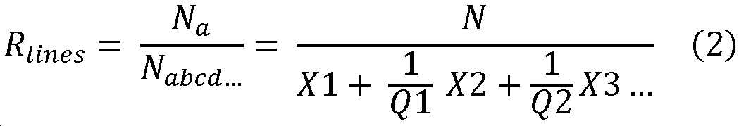
![]()
![]()
데이터 밀도data density
더욱이, 모든 N개의 영역들이 라인 밀도 a 인 경우의 데이터 밀도 (Na) 와, N 이 a 및 b 로 구성되는 경우의 데이터 밀도 (Nab) 를 비교한 비율 (Rdata) 이 식 (3) 에 제시된 바와 같다고 나타내어질 수 있으며, X 및 Y 는, 각각, 소스 및 게이트 라인들에 대해 밀도 a 를 갖는 영역들의 수이다:Furthermore, the ratio (R data ) comparing the data density (N a ) when all N regions are the line density a and the data density (N ab ) when N is composed of a and b is expressed in Equation (3) can be shown as given in , where X and Y are the number of regions with density a for the source and gate lines, respectively:
![]()
![]()
X 및 Y 가 최대로 N, 즉, 전극 밀도 a 일 수 있는 구동기 또는 소스 측 중 어느 하나를 따른 영역들의 수, 와 동일할 수 있기 때문에, 곱 XY ≤ N2 임을 유의해야 한다. 감소하는 X 및 Y 에 대해, 비율은 Q2 에 접근한다. 큰 X 에 대해, 비율은 1 의 값에 접근한다. 요컨대, 가변 전극 사이즈 영역들로부터 도출되는 이점들은, 소스/게이트 구동기 복잡도가 Q 의 값에 접근하는 것과 데이터 복잡도가 Q2 의 값에 근접하는 것을 포함한다.It should be noted that the product XY ≤ N 2 , since X and Y may be at most equal to N, ie, the number of regions along either the driver or source side, which may be electrode density a . For decreasing X and Y, the ratio approaches Q 2 . For large Xs, the ratio approaches a value of 1. In short, the benefits derived from variable electrode size regions include source/gate driver complexity approaching the value of Q and data complexity approaching the value of Q 2 .
예시적인 아키텍처들Exemplary Architectures
실시예 1Example 1
도 1 의 다이어그램은 예시적인 가변 사이즈 전극 어레이의 구조를 예시한다. 어레이는 3개의 영역들 (10, 12 및 14) 로 파티셔닝되고, 여기서, 각각의 영역의 서브어레이는 그 개별 구동 라인 밀도 (a, b 또는 c) 에 의해 정의된다. 도 1 의 영역들이 동일한 행 및 열 라인 밀도를 갖지만, 이는 요건은 아니다. 예를 들어, 영역 (10) 은, 당해 어플리케이션의 요건들에 의존하여, 행 라인 밀도 a 와, 또한, a 보다 크거나 작을 수도 있는 열 라인 밀도 a* 에 의해 특징지어질 수도 있다. 일 예시적인 구현에 있어서, 저밀도 영역들은 고밀도 영역으로부터 멀리 분기한다. 부가적으로, 원한다면, 게이트 및 소스 라인들은, 고밀도 라인들로부터 발생하는 더 낮은 밀도 영역들에서의 여분의 커패시턴스를 회피하기 위해 어레이로 더 깊게 나아감에 따라, 원하는 밀도를 위해 조정하기 위해 종단될 수도 있다. 이러한 설계 특징의 이점은, 감소된 게이트 및/또는 소스 라인 요건에서 그리고 더 적은 데이터 프로세싱으로 어레이 상에서 고해상도 동작들을 실행하는 능력이다.The diagram of FIG. 1 illustrates the structure of an exemplary variable size electrode array. The array is partitioned into three
소스 및 구동기 라인들에 대한 예시적인 라우팅이 도 5 에 도시된다. 선호된 실시형태에 있어서, 고밀도 구동 전극들 (42) 의 영역들은 소스 및 게이트 구동기들에 더 가깝게 분포되고, 저밀도 구동 전극들 (44) 의 영역들은 고밀도 영역들로부터 팬아웃된다. 게이트 구동 라인들 (47) 은 게이트 구동기 (45) 로부터 이어지고, 소스 구동 라인들 (48) 은 소스 구동기 (46) 로부터 이어진다. (특히, 각각의 구동 전극을 제어하는 박막 트랜지스터들은 도 5 에 도시되지 않는다. 도 5 에서, TFT 는 각각의 구동 전극의 상좌측 코너에 위치될 것이다.). 도 5 의 실시형태에 있어서, 다중의 게이트 구동기 라인들 (47) 및 다중의 소스 구동기 라인들 (48) 은, 도 5 에서 타원 (49) 에 의해 강조된 바와 같이 조기에 종단된다. 즉, 특정 구동기 라인들은 전체 어레이에 걸쳐 연장되지 않는데, 왜냐하면 구동기 라인 종단을 지나 제어할 추가의 TFT들이 없기 때문이다. 본 발명의 실시형태들에 있어서, 이러한 아키텍처는 구동 전극들 (42, 44) 의 다양한 밀도에도 불구하고 단일 게이트 구동기 (45) 및 단일 소스 구동기 (46) 가 전체 어레이를 구동하게 한다. 픽셀을 활성화시키기 위해 신호가 생성될 수도 있지만, 더 낮은 밀도 영역들에서 전극을 에너자이징하기 위해 TFT 에서 소스 및 게이트 구동기 신호가 동시에 존재하지 않을 것이다. 더욱이, 게이트 구동기 라인들 (47) 및 소스 구동기 라인들 (48) 을 조기에 종단시킴으로써, 저밀도 전극들 (44) 과 게이트 구동기 라인들 (47) 및 소스 구동기 라인들 (48) 사이에 더 적은 용량성 커플링이 존재하며, 이들 라인들은, 그렇지 않으면 저밀도 전극들 (44) 아래로 이어질 것이다. 다른 경우들에서, 단일 구동기 라인은 하나의 사이즈 및 밀도의 전극들에만 걸쳐 있을 수도 있다. 도 5 에 도시된 바와 같이, 하나의 코너에서 시작하는 고밀도 구동 전극들 (42) 을 배열하는 것은 고밀도 구동 전극들 (42) 의 제 1 정사각형 어레이 (도 5 에서 4x4) 의 자연 패턴을 발생시켜, 균일하게 이격된 저밀도 구동 전극들 (44) 을 유도한다. 이러한 배열에서, 짝수개의 게이트 구동기 라인들 (47) 과 소스 구동기 라인들 (48) 은 조기 종단된다.An exemplary routing for the source and driver lines is shown in FIG. 5 . In a preferred embodiment, regions of high
실시예 2Example 2
도 6 에, 다른 예시적인 가변 사이즈 어레이의 구조가 예시된다. 영역 (50) 은 라인 밀도 (행 및 열) a 이고, 영역 (52) 은 라인 밀도 b 이다. 라인 밀도 a 는 b 보다 크다. 그에 따라, 예를 들어 100 mm2 당 전극들의 수의 관점에서 표현된 바와 같이, D1 이 영역 (50) 의 전극 밀도로서 정의되고, D2 가 영역 (52) 의 전극 밀도로서 정의되면, 비율 D1 : D2 는 1 의 값을 초과한다. 대표적인 실시형태들에 있어서, 비율 D1 : D2 는 약 2n 과 동일하여 (n 은 자연수), 정사각형 전극 포맷을 유지한다. 예를 들어, 비율 D1 : D2 는, 당해 어플리케이션에 적합하도록, 약 2, 4, 8, 또는 16 과 동일할 수도 있다. AM-EWoD 디바이스들에서의 개별 전극들의 사이즈는 일반적으로, 약 50 ㎛ 내지 약 600 ㎛ 의 범위에 속한다. 따라서, 영역 (52) 의 전극들이 사이즈가 600 ㎛ 이면, 영역 (50) 의 전극들은, 원하는 비율 D1 : D2 가 2, 4, 또는 8 인지 여부에 의존하여, 300, 150, 또는 75 ㎛ 일 수도 있다.6 , the structure of another exemplary variable size array is illustrated.
D1 : D2 비율이 3, 5, 6, 7, 9, 또는 2n 과 동일하지 않은 다른 정수들과 동일한 실시형태들이 또한 고려된다. 일 사례에서, 영역 (50) 전극들의 사이즈는 약 25 ㎛ 내지 약 200 ㎛ 의 범위일 수도 있는 한편, 영역 (52) 의 전극들은 약 100 ㎛ 내지 약 800 ㎛ 의 범위에 속할 수도 있다. 이에 따라, 영역 (50) 의 전극들이 사이즈가 50 ㎛ 이면, 비율 D1 : D2 는, 영역 (52) 의 전극들에 대해 선택된 사이즈에 의존하여, 2, 3, 4, 5, 6, 7 등일 수도 있다.Embodiments where the ratio D1 : D2 equals 3, 5, 6, 7, 9, or other integers not equal to 2 n are also contemplated. In one instance, the size of the electrodes of
일 실시형태에 있어서, 영역 (50) 은 어레이의 상부 및 좌측 에지들에 더 가깝게 배치되고, 그로부터, 밀도는 에지들로부터 멀리 이동하면서 감소한다. 이러한 배치는, 영역 (50) 으로부터 영역 (52) 으로 교차할 때 서브어레이들의 라인 밀도를 감소시키는 것을 가능케 한다. 대안적으로, 라인 밀도는 각각의 행 또는 열을 따라 일정하게 유지될 수도 있지만, 픽셀들 자체에 대한 연결들은 이루어지지 않는다.In one embodiment,
실시예 3Example 3
도 7 의 개략도는 예시적인 AM-EWoD 디바이스 (60) 를 예시한다. 저장소들 (R1) 은 제 1 타입의 유체를, 저장소들 (R2) 은 제 2 타입의 유체를, 그리고 저장소 (R3) 는 제 3 타입의 유체를 함유한다. 디바이스의 TFT 어레이는 저장소 유입구들 부근에 높은 전극 밀도 영역들 (62) 을 포함하여, 샘플 액적들이 저장소로부터 취해지고 높은 전극 밀도 영역의 표면 상에 디포짓될 수 있다. 영역들 (62) 의 서브어레이들의 높은 전극 밀도는, 높은 정확도로 샘플 액적들의 희석, 혼합, 및 사이징 (분할) 과 같은 분석 단계들을 실행할 수 있게 한다. 일 예시적인 실시형태에 있어서, 피분석물의 존재 및 선택적으로 농도에 대해 분석될 샘플 액적은 용매의 하나 이상의 액적들과의 조합에 의해 희석되고, 희석 단계는, 원하는 피분석물 농도 범위가 획득될 때까지 반복될 수도 있다. 그 다음, 희석된 샘플의 액적은, 피분석물과 함께 검출가능하고 정량가능한 분석 생성물을 형성하는 하나 이상의 반응물들의 액적(들)과 혼합된다.The schematic diagram of FIG. 7 illustrates an example AM-EWoD device 60 . Reservoirs R1 contain a fluid of a first type, reservoirs R2 contain a fluid of a second type, and reservoir R3 contain a fluid of a third type. The TFT array of the device includes high
그 후, 샘플 액적들은 분석 생성물의 농도를 검출하고 측정하기 위해 저해상도 구역 (63) 으로 전송될 수도 있다. 예시적인 검출 및 측정 기법들은 가시, UV, 및 IR 범위들의 분광광도법, 시간 분해 분광법, 형광 분광법, 라만 분광법, 인광 분광법, 및 순환 전압전류법 (CV) 과 같은 전위역학 전기화학적 측정들을 포함한다. 피분석물이 진단 바이오마커, 예를 들어, 주어진 질환 또는 장애와 연관된 단백질인 경우들에서, 샘플 액적은 측정될 단백질에 대해 지향된 항체를 함유하는 용액의 액적과 혼합될 수도 있다. 효소 결합된 면역흡착 분석 (ELISA) 에서, 항체가 효소에 결합되고, 이 때, 효소의 기질을 포함하는 물질의 다른 액적이 첨가된다. 후속 반응은 검출가능한 신호, 가장 일반적으로는, 저해상도 영역에서의 하나 이상의 픽셀들에서 검출 및 측정될 수도 있는 색상 변화를 생성한다.Thereafter, the sample droplets may be sent to the low resolution zone 63 to detect and measure the concentration of the analyte product. Exemplary detection and measurement techniques include electrodynamic electrochemical measurements such as spectrophotometry in the visible, UV, and IR ranges, time-resolved spectroscopy, fluorescence spectroscopy, Raman spectroscopy, phosphorescence spectroscopy, and cyclic voltammetry (CV). In cases where the analyte is a diagnostic biomarker, eg, a protein associated with a given disease or disorder, a sample droplet may be mixed with a droplet of a solution containing an antibody directed against the protein to be measured. In an enzyme linked immunosorbent assay (ELISA), an antibody is bound to an enzyme, in which case another droplet of material comprising the enzyme's substrate is added. The subsequent reaction produces a detectable signal, most typically a color change that may be detected and measured in one or more pixels in the low resolution region.
샘플 액적들의 평균 직경이 길이에 있어서 약 n개의 고해상도 픽셀들을 측정한다면, 고밀도 영역은, 바람직하게, 액적 조작을 위한 충분한 공간을 제공하기 위하여 적어도 2n개의 픽셀들을 포함할 것이다. 고해상도 영역들을 생성하는데 전용되는 소스 및/또는 구동 라인들의 몫을 전체의 약 25% 내지 50% 로 제한함으로써, 게이트 및/또는 소스 구동기 복잡도가 감소되며, 데이터 복잡도도 감소된다. 이는, 차례로, 약 30% 내지 60% 의 게이트/소스 요건 감소 및 데이터 양의 2.3 내지 3.4배 감소를 의미한다.If the average diameter of the sample droplets measures about n high resolution pixels in length, then the high density region will preferably contain at least 2n pixels to provide sufficient space for droplet manipulation. By limiting the share of source and/or drive lines dedicated to creating high resolution regions to about 25% to 50% of the total, gate and/or source driver complexity is reduced, and data complexity is also reduced. This, in turn, means a reduction in gate/source requirements of about 30% to 60% and a 2.3 to 3.4 fold reduction in the amount of data.
전술한 바로부터, 본 발명은 보증된 영역에서만 고 복잡도를 갖는 디바이스를 제공할 수 있고, 이에 의해, 전체 복잡도를 최소로 유지할 수 있고, 제조 및 동작 비용을 동일하게 낮출 수 있음을 알 수 있을 것이다. 다수의 변경들 및 수정들이 본 발명의 범위로부터 일탈함 없이 상기 설명된 본 발명의 특정 실시형태들에서 이루어질 수 있음이 당업자에게 자명할 것이다. 이에 따라, 전술한 설명의 전부는 한정적인 의미가 아닌 예시적인 의미로 해석되어야 한다.From the foregoing, it will be seen that the present invention can provide a device with high complexity only in a guaranteed area, thereby keeping the overall complexity to a minimum and lowering the manufacturing and operating costs equally. . It will be apparent to those skilled in the art that numerous changes and modifications can be made in the specific embodiments of the invention described above without departing from the scope of the invention. Accordingly, all of the above description should be interpreted in an illustrative rather than a restrictive sense.
Claims (20)
(i) 기판으로서,
제 1 밀도 (D1) (전극들/단위면적) 를 갖는 제 1 복수의 전극들과,
상기 제 1 복수의 전극들에 커플링된 박막 트랜지스터들의 제 1 세트를 포함하는,
제 1 고해상도 영역;
제 2 밀도 (D2) (전극들/단위면적) 를 갖는 제 2 복수의 전극들로서, D2 < D1 인, 상기 제 2 복수의 전극들과,
상기 제 2 복수의 전극들에 커플링된 박막 트랜지스터들의 제 2 세트를 포함하는,
제 2 저해상도 영역; 및
상기 제 1 및 제 2 복수의 전극들 뿐 아니라 상기 박막 트랜지스터들의 제 1 및 제 2 세트들 양자 모두를 커버하는 소수성 층을 포함하는, 상기 기판; 및
(ii) 상기 박막 트랜지스터들의 제 1 세트 및 제 2 세트에 동작가능하게 커플링되고, 상기 제 1 복수의 전극들의 적어도 일부 및 상기 제 2 복수의 전극들의 적어도 일부에 추진 전압을 제공하도록 구성되는 제어기를 포함하는, 디지털 미세유체 디바이스.A digital microfluidic device comprising:
(i) a substrate comprising:
a first plurality of electrodes having a first density D1 (electrodes/unit area);
a first set of thin film transistors coupled to the first plurality of electrodes;
a first high-resolution region;
a second plurality of electrodes having a second density D2 (electrodes/unit area), wherein D2 <D1;
a second set of thin film transistors coupled to the second plurality of electrodes;
a second low-resolution region; and
the substrate comprising a hydrophobic layer covering both the first and second sets of thin film transistors as well as the first and second plurality of electrodes; and
(ii) a controller operatively coupled to the first and second sets of thin film transistors and configured to provide a propulsion voltage to at least a portion of the first plurality of electrodes and at least a portion of the second plurality of electrodes A digital microfluidic device comprising a.
비율 D1 : D2 는 2n 과 동일하고, n 은 자연수인, 디지털 미세유체 디바이스.The method of claim 1,
A digital microfluidic device, wherein the ratio D1 : D2 is equal to 2 n and n is a natural number.
비율 D1 : D2 는 2, 4, 8, 또는 16 과 동일한, 디지털 미세유체 디바이스.3. The method of claim 2,
A digital microfluidic device, wherein the ratio D1 : D2 is equal to 2, 4, 8, or 16.
비율 D1 : D2 는 3, 5, 6, 7, 또는 9 와 동일한, 디지털 미세유체 디바이스.The method of claim 1,
A digital microfluidic device, wherein the ratio D1 : D2 is equal to 3, 5, 6, 7, or 9.
상기 제 1 복수의 전극들은 사이즈가 약 25 ㎛ 내지 약 200 ㎛ 인, 디지털 미세유체 디바이스.The method of claim 1,
wherein the first plurality of electrodes have a size of about 25 μm to about 200 μm.
상기 제 2 복수의 전극들은 사이즈가 약 100 ㎛ 내지 약 800 ㎛ 인, 디지털 미세유체 디바이스.The method of claim 1,
wherein the second plurality of electrodes have a size of about 100 μm to about 800 μm.
상기 제 1 고해상도 영역은 상기 제 2 저해상도 영역보다 작은, 디지털 미세유체 디바이스.The method of claim 1,
wherein the first high resolution region is smaller than the second low resolution region.
상기 제 1 복수의 전극들은 정사각형 또는 직사각형 서브어레이로 배열되는, 디지털 미세유체 디바이스.The method of claim 1,
wherein the first plurality of electrodes are arranged in a square or rectangular subarray.
상기 소수성 층과 상기 제 1 및 제 2 복수의 전극들 사이에 개재된 유전체 층을 더 포함하는, 디지털 미세유체 디바이스.The method of claim 1,
and a dielectric layer interposed between the hydrophobic layer and the first and second plurality of electrodes.
저장소 유출구를 통해 상기 제 1 고해상도 영역에 동작가능하게 연결된 유체 저장소를 더 포함하는, 디지털 미세유체 디바이스.The method of claim 1,
The digital microfluidic device further comprising a fluid reservoir operatively connected to the first high resolution region through a reservoir outlet.
상기 제 1 밀도 (D1) (전극들/단위면적) 의 제 3 복수의 전극들을 포함하는 제 2 고해상도 영역,
상기 제 3 복수의 전극들에 커플링된 박막 트랜지스터들의 제 3 세트, 및
상기 제 2 고해상도 영역에 동작가능하게 연결된 제 2 저장소를 더 포함하는, 디지털 미세유체 디바이스.The method of claim 1,
a second high-resolution region comprising a third plurality of electrodes of said first density D1 (electrodes/unit area);
a third set of thin film transistors coupled to the third plurality of electrodes; and
and a second reservoir operatively coupled to the second high resolution region.
단일 상부 전극, 상기 단일 상부 전극을 커버하는 상부 소수성 층, 및 상기 소수성 층과 상기 상부 소수성 층을 분리하고 그리고 상기 소수성 층과 상기 상부 소수성 층 사이에 미세유체 셀 갭을 생성하는 스페이서를 더 포함하는, 디지털 미세유체 디바이스.The method of claim 1,
A single upper electrode, an upper hydrophobic layer covering the single upper electrode, and a spacer separating the hydrophobic layer and the upper hydrophobic layer and creating a microfluidic cell gap between the hydrophobic layer and the upper hydrophobic layer , digital microfluidic devices.
상기 상부 소수성 층과 상기 단일 상부 전극 사이에 개재된 상부 유전체 층을 더 포함하는, 디지털 미세유체 디바이스.13. The method of claim 12,
and an upper dielectric layer interposed between the upper hydrophobic layer and the single upper electrode.
상기 셀 갭은 약 20 ㎛ 내지 500 ㎛ 인, 디지털 미세유체 디바이스.13. The method of claim 12,
wherein the cell gap is between about 20 μm and 500 μm.
상기 상부 전극은 적어도 하나의 광 투과성 영역을 포함하는, 디지털 미세유체 디바이스.13. The method of claim 12,
wherein the upper electrode comprises at least one light transmissive region.
상기 광 투과성 영역은 면적이 적어도 10 mm2 인, 디지털 미세유체 디바이스.16. The method of claim 15,
wherein the light transmissive region has an area of at least 10 mm 2 .
(i) 기판으로서,
제 1 복수의 전극들로서, 상기 제 1 복수의 전극들의 각각은 제 1 복수의 소스 라인들과 전기 통신하고, 상기 제 1 복수의 소스 라인들은 D1 (소스 라인들/단위면적) 의 제 1 소스 라인 밀도를 갖는, 상기 제 1 복수의 전극들과,
상기 제 1 복수의 전극들 및 상기 제 1 복수의 소스 라인들에 커플링된 박막 트랜지스터들의 제 1 세트를 포함하는,
제 1 고해상도 영역;
제 2 복수의 전극들로서, 상기 제 2 복수의 전극들의 각각은 제 2 복수의 소스 라인들과 전기 통신하고, 상기 제 2 복수의 소스 라인들은 D2 (소스 라인들/단위면적) 의 제 2 소스 라인 밀도를 갖고, D1 > D2 인, 상기 제 2 복수의 전극들과,
상기 제 2 복수의 전극들 및 상기 제 2 복수의 소스 라인들에 커플링된 박막 트랜지스터들의 제 2 세트를 포함하는,
제 2 저해상도 영역; 및
상기 제 1 및 제 2 복수의 전극들 뿐 아니라 상기 박막 트랜지스터들의 제 1 및 제 2 세트들 양자 모두를 커버하는 소수성 층을 포함하는, 상기 기판; 및
(ii) 상기 제 1 복수의 소스 라인들 및 상기 제 2 복수의 소스 라인들에 동작가능하게 커플링되고, 상기 제 1 복수의 전극들의 적어도 일부 및 상기 제 2 복수의 전극들의 적어도 일부에 소스 전압을 제공하도록 구성되는 소스 구동기를 포함하고,
상기 제 2 복수의 소스 라인들의 적어도 일부는 상기 제 1 복수의 소스 라인들 중 하나에 연결되는, 디지털 미세유체 디바이스.A digital microfluidic device comprising:
(i) a substrate comprising:
a first plurality of electrodes, each of the first plurality of electrodes being in electrical communication with a first plurality of source lines, the first plurality of source lines having a first source line of D1 (source lines/unit area) the first plurality of electrodes having a density;
a first set of thin film transistors coupled to the first plurality of electrodes and to the first plurality of source lines;
a first high-resolution region;
a second plurality of electrodes, each of the second plurality of electrodes being in electrical communication with a second plurality of source lines, the second plurality of source lines being a second source line of D2 (source lines/unit area) said second plurality of electrodes having a density, wherein D1 >D2;
a second set of thin film transistors coupled to the second plurality of electrodes and the second plurality of source lines;
a second low-resolution region; and
the substrate comprising a hydrophobic layer covering both the first and second sets of thin film transistors as well as the first and second plurality of electrodes; and
(ii) operatively coupled to the first plurality of source lines and the second plurality of source lines, the source voltage to at least a portion of the first plurality of electrodes and at least a portion of the second plurality of electrodes A source driver configured to provide
at least a portion of the second plurality of source lines is coupled to one of the first plurality of source lines.
상기 디바이스의 상기 제 1 고해상도 영역의 표면 상에 샘플 액적을 디포짓하는 단계;
상기 액적에 희석, 혼합, 사이징, 및 이들의 조합들로 이루어진 군으로부터 선택된 하나 이상의 프로세싱 단계들을 실시하여 분석 생성물을 형성하는 단계;
상기 생성물의 액적을 상기 디바이스의 상기 저해상도 영역의 표면에 전송하는 단계;
상기 분석 생성물을 검출하는 단계; 및
선택적으로 상기 분석 생성물의 농도를 측정하는 단계를 포함하는, 샘플에서의 피분석물을 분석하기 위한 방법.A method for analyzing an analyte in a sample with the digital microfluidic device according to claim 1, comprising:
depositing a sample droplet on a surface of the first high resolution region of the device;
subjecting the droplets to one or more processing steps selected from the group consisting of dilution, mixing, sizing, and combinations thereof to form an analyte;
transferring droplets of the product to the surface of the low resolution region of the device;
detecting the analyte product; and
optionally measuring the concentration of the analyte product.
상기 피분석물은 진단 바이오마커인, 샘플에서의 피분석물을 분석하기 위한 방법.19. The method of claim 18,
The method for analyzing an analyte in a sample, wherein the analyte is a diagnostic biomarker.
상기 혼합은 상기 진단 바이오마커와 매칭하는 항체를 함유한 용액의 액적과 되는, 샘플에서의 피분석물을 분석하기 위한 방법.20. The method of claim 19,
wherein said mixing is with a droplet of a solution containing an antibody that matches said diagnostic biomarker.
Applications Claiming Priority (3)
| Application Number | Priority Date | Filing Date | Title |
|---|---|---|---|
| US201962943295P | 2019-12-04 | 2019-12-04 | |
| US62/943,295 | 2019-12-04 | ||
| PCT/US2020/063074 WO2021113485A1 (en) | 2019-12-04 | 2020-12-03 | Variable electrode size area arrays on thin-film transistor based digital microfluidic devices for fine droplet manipulation |
Publications (1)
| Publication Number | Publication Date |
|---|---|
| KR20220110517A true KR20220110517A (en) | 2022-08-08 |
Family
ID=76209388
Family Applications (1)
| Application Number | Title | Priority Date | Filing Date |
|---|---|---|---|
| KR1020227022145A Withdrawn KR20220110517A (en) | 2019-12-04 | 2020-12-03 | Variable Electrode Size Area Arrays on Thin Film Transistor-Based Digital Microfluidic Devices for Precise Droplet Manipulation |
Country Status (7)
| Country | Link |
|---|---|
| US (1) | US20210170413A1 (en) |
| EP (1) | EP4069425A4 (en) |
| JP (1) | JP2023504518A (en) |
| KR (1) | KR20220110517A (en) |
| CN (1) | CN114746183A (en) |
| TW (1) | TWI800773B (en) |
| WO (1) | WO2021113485A1 (en) |
Families Citing this family (2)
| Publication number | Priority date | Publication date | Assignee | Title |
|---|---|---|---|---|
| US11727957B1 (en) | 2022-06-10 | 2023-08-15 | Seagate Technology Llc | Data storage drive with a vertically translatable actuator arm |
| TWI806764B (en) * | 2022-09-12 | 2023-06-21 | 友達光電股份有限公司 | Electrowetting-on-dielectric device |
Family Cites Families (12)
| Publication number | Priority date | Publication date | Assignee | Title |
|---|---|---|---|---|
| KR20090027254A (en) * | 2004-10-14 | 2009-03-16 | 가부시끼가이샤 도시바 | FET-based nucleic acid detection sensor |
| US20100120130A1 (en) * | 2007-08-08 | 2010-05-13 | Advanced Liquid Logic, Inc. | Droplet Actuator with Droplet Retention Structures |
| JP2009065146A (en) * | 2007-08-15 | 2009-03-26 | Sony Corp | Semiconductor thin film forming method and semiconductor thin film inspection apparatus |
| CN102671723B (en) * | 2011-02-17 | 2015-03-11 | 王崇智 | Method of manipulating droplet on ewod microelectrode array architecture |
| CN102866193B (en) * | 2012-09-04 | 2015-04-01 | 吴传勇 | Device and method for controlling particles in liquid based on dielectrophoresis |
| US9254485B2 (en) * | 2012-12-17 | 2016-02-09 | Taiwan Semiconductor Manufacturing Company, Ltd. | Systems and methods for an integrated bio-entity manipulation and processing device |
| WO2016100521A1 (en) * | 2014-12-18 | 2016-06-23 | Life Technologies Corporation | Methods and apparatus for measuring analytes using large scale fet arrays |
| JP6494580B2 (en) * | 2016-09-28 | 2019-04-03 | シャープ ライフ サイエンス (イーユー) リミテッド | Microfluidic device |
| US10369570B2 (en) * | 2017-07-27 | 2019-08-06 | Sharp Life Science (Eu) Limited | Microfluidic device with droplet pre-charge on input |
| CN107497509B (en) * | 2017-10-11 | 2020-05-26 | 京东方科技集团股份有限公司 | Microfluidic system and driving method thereof |
| US10882042B2 (en) * | 2017-10-18 | 2021-01-05 | E Ink Corporation | Digital microfluidic devices including dual substrates with thin-film transistors and capacitive sensing |
| CN108855266B (en) * | 2018-07-23 | 2020-07-28 | 京东方科技集团股份有限公司 | Droplet moving device, microfluidic system and working method thereof |
-
2020
- 2020-12-03 CN CN202080084025.8A patent/CN114746183A/en active Pending
- 2020-12-03 JP JP2022533124A patent/JP2023504518A/en active Pending
- 2020-12-03 KR KR1020227022145A patent/KR20220110517A/en not_active Withdrawn
- 2020-12-03 US US17/110,896 patent/US20210170413A1/en not_active Abandoned
- 2020-12-03 WO PCT/US2020/063074 patent/WO2021113485A1/en not_active Ceased
- 2020-12-03 EP EP20897063.2A patent/EP4069425A4/en not_active Withdrawn
- 2020-12-04 TW TW109142831A patent/TWI800773B/en active
Also Published As
| Publication number | Publication date |
|---|---|
| EP4069425A1 (en) | 2022-10-12 |
| WO2021113485A1 (en) | 2021-06-10 |
| TW202135941A (en) | 2021-10-01 |
| TWI800773B (en) | 2023-05-01 |
| JP2023504518A (en) | 2023-02-03 |
| US20210170413A1 (en) | 2021-06-10 |
| EP4069425A4 (en) | 2023-11-08 |
| CN114746183A (en) | 2022-07-12 |
Similar Documents
| Publication | Publication Date | Title |
|---|---|---|
| US20250065326A1 (en) | Directing motion of droplets using differential wetting | |
| CN115007233B (en) | Digital microfluidic devices including dual substrates with thin film transistors and capacitive sensing | |
| CN101679078B (en) | Digital Microfluidics Based on Electrowetting | |
| US20040231987A1 (en) | Method, apparatus and article for microfluidic control via electrowetting, for chemical, biochemical and biological assays and the like | |
| US20250199292A1 (en) | Spatially variable hydrophobic layers for digital microfluidics | |
| US20210394190A1 (en) | Intermittent driving patterns for extended holding of droplets in a digital microfluidic device | |
| CN108686726A (en) | Drop actuating method for microfluidic device | |
| US11410620B2 (en) | Adaptive gate driving for high frequency AC driving of EWoD arrays | |
| KR20220110517A (en) | Variable Electrode Size Area Arrays on Thin Film Transistor-Based Digital Microfluidic Devices for Precise Droplet Manipulation | |
| US11554374B2 (en) | Spatially variable dielectric layers for digital microfluidics | |
| TW202306647A (en) | Digital microfluidic device with capacitive sensing | |
| US11596946B2 (en) | Segmented top plate for variable driving and short protection for digital microfluidics | |
| US11806715B2 (en) | Method of electrowetting | |
| US20230241606A1 (en) | Liquid sample recovery in high density digital microfluidic arrays | |
| US20220008921A1 (en) | Spatial and temporal necking for robust multi-size dispensing of liquids on high electrode density electro-wetting arrays |
Legal Events
| Date | Code | Title | Description |
|---|---|---|---|
| PA0105 | International application |
St.27 status event code: A-0-1-A10-A15-nap-PA0105 |
|
| PG1501 | Laying open of application |
St.27 status event code: A-1-1-Q10-Q12-nap-PG1501 |
|
| R18-X000 | Changes to party contact information recorded |
St.27 status event code: A-3-3-R10-R18-oth-X000 |
|
| PC1203 | Withdrawal of no request for examination |
St.27 status event code: N-1-6-B10-B12-nap-PC1203 |