KR20210104201A - Organic light-emitting display device - Google Patents
Organic light-emitting display device Download PDFInfo
- Publication number
- KR20210104201A KR20210104201A KR1020200018185A KR20200018185A KR20210104201A KR 20210104201 A KR20210104201 A KR 20210104201A KR 1020200018185 A KR1020200018185 A KR 1020200018185A KR 20200018185 A KR20200018185 A KR 20200018185A KR 20210104201 A KR20210104201 A KR 20210104201A
- Authority
- KR
- South Korea
- Prior art keywords
- light emitting
- organic light
- emitting diode
- display area
- display
- Prior art date
- Legal status (The legal status is an assumption and is not a legal conclusion. Google has not performed a legal analysis and makes no representation as to the accuracy of the status listed.)
- Pending
Links
Images


Classifications
-
- H—ELECTRICITY
- H10—SEMICONDUCTOR DEVICES; ELECTRIC SOLID-STATE DEVICES NOT OTHERWISE PROVIDED FOR
- H10K—ORGANIC ELECTRIC SOLID-STATE DEVICES
- H10K59/00—Integrated devices, or assemblies of multiple devices, comprising at least one organic light-emitting element covered by group H10K50/00
- H10K59/30—Devices specially adapted for multicolour light emission
- H10K59/35—Devices specially adapted for multicolour light emission comprising red-green-blue [RGB] subpixels
- H10K59/352—Devices specially adapted for multicolour light emission comprising red-green-blue [RGB] subpixels the areas of the RGB subpixels being different
-
- H—ELECTRICITY
- H10—SEMICONDUCTOR DEVICES; ELECTRIC SOLID-STATE DEVICES NOT OTHERWISE PROVIDED FOR
- H10K—ORGANIC ELECTRIC SOLID-STATE DEVICES
- H10K59/00—Integrated devices, or assemblies of multiple devices, comprising at least one organic light-emitting element covered by group H10K50/00
- H10K59/10—OLED displays
- H10K59/12—Active-matrix OLED [AMOLED] displays
- H10K59/121—Active-matrix OLED [AMOLED] displays characterised by the geometry or disposition of pixel elements
-
- H01L27/3218—
-
- H01L27/3225—
-
- H01L27/3244—
-
- H01L51/52—
-
- H—ELECTRICITY
- H10—SEMICONDUCTOR DEVICES; ELECTRIC SOLID-STATE DEVICES NOT OTHERWISE PROVIDED FOR
- H10K—ORGANIC ELECTRIC SOLID-STATE DEVICES
- H10K50/00—Organic light-emitting devices
- H10K50/10—OLEDs or polymer light-emitting diodes [PLED]
- H10K50/11—OLEDs or polymer light-emitting diodes [PLED] characterised by the electroluminescent [EL] layers
- H10K50/125—OLEDs or polymer light-emitting diodes [PLED] characterised by the electroluminescent [EL] layers specially adapted for multicolour light emission, e.g. for emitting white light
- H10K50/13—OLEDs or polymer light-emitting diodes [PLED] characterised by the electroluminescent [EL] layers specially adapted for multicolour light emission, e.g. for emitting white light comprising stacked EL layers within one EL unit
-
- H—ELECTRICITY
- H10—SEMICONDUCTOR DEVICES; ELECTRIC SOLID-STATE DEVICES NOT OTHERWISE PROVIDED FOR
- H10K—ORGANIC ELECTRIC SOLID-STATE DEVICES
- H10K50/00—Organic light-emitting devices
- H10K50/10—OLEDs or polymer light-emitting diodes [PLED]
- H10K50/14—Carrier transporting layers
- H10K50/15—Hole transporting layers
-
- H—ELECTRICITY
- H10—SEMICONDUCTOR DEVICES; ELECTRIC SOLID-STATE DEVICES NOT OTHERWISE PROVIDED FOR
- H10K—ORGANIC ELECTRIC SOLID-STATE DEVICES
- H10K50/00—Organic light-emitting devices
- H10K50/10—OLEDs or polymer light-emitting diodes [PLED]
- H10K50/14—Carrier transporting layers
- H10K50/16—Electron transporting layers
-
- H—ELECTRICITY
- H10—SEMICONDUCTOR DEVICES; ELECTRIC SOLID-STATE DEVICES NOT OTHERWISE PROVIDED FOR
- H10K—ORGANIC ELECTRIC SOLID-STATE DEVICES
- H10K50/00—Organic light-emitting devices
- H10K50/10—OLEDs or polymer light-emitting diodes [PLED]
- H10K50/17—Carrier injection layers
- H10K50/171—Electron injection layers
-
- H—ELECTRICITY
- H10—SEMICONDUCTOR DEVICES; ELECTRIC SOLID-STATE DEVICES NOT OTHERWISE PROVIDED FOR
- H10K—ORGANIC ELECTRIC SOLID-STATE DEVICES
- H10K59/00—Integrated devices, or assemblies of multiple devices, comprising at least one organic light-emitting element covered by group H10K50/00
- H10K59/10—OLED displays
- H10K59/12—Active-matrix OLED [AMOLED] displays
- H10K59/122—Pixel-defining structures or layers, e.g. banks
-
- H—ELECTRICITY
- H10—SEMICONDUCTOR DEVICES; ELECTRIC SOLID-STATE DEVICES NOT OTHERWISE PROVIDED FOR
- H10K—ORGANIC ELECTRIC SOLID-STATE DEVICES
- H10K59/00—Integrated devices, or assemblies of multiple devices, comprising at least one organic light-emitting element covered by group H10K50/00
- H10K59/30—Devices specially adapted for multicolour light emission
- H10K59/35—Devices specially adapted for multicolour light emission comprising red-green-blue [RGB] subpixels
- H10K59/353—Devices specially adapted for multicolour light emission comprising red-green-blue [RGB] subpixels characterised by the geometrical arrangement of the RGB subpixels
-
- H—ELECTRICITY
- H10—SEMICONDUCTOR DEVICES; ELECTRIC SOLID-STATE DEVICES NOT OTHERWISE PROVIDED FOR
- H10K—ORGANIC ELECTRIC SOLID-STATE DEVICES
- H10K59/00—Integrated devices, or assemblies of multiple devices, comprising at least one organic light-emitting element covered by group H10K50/00
- H10K59/10—OLED displays
- H10K59/12—Active-matrix OLED [AMOLED] displays
- H10K59/131—Interconnections, e.g. wiring lines or terminals
-
- H—ELECTRICITY
- H10—SEMICONDUCTOR DEVICES; ELECTRIC SOLID-STATE DEVICES NOT OTHERWISE PROVIDED FOR
- H10K—ORGANIC ELECTRIC SOLID-STATE DEVICES
- H10K59/00—Integrated devices, or assemblies of multiple devices, comprising at least one organic light-emitting element covered by group H10K50/00
- H10K59/60—OLEDs integrated with inorganic light-sensitive elements, e.g. with inorganic solar cells or inorganic photodiodes
- H10K59/65—OLEDs integrated with inorganic image sensors
Landscapes
- Physics & Mathematics (AREA)
- Optics & Photonics (AREA)
- Engineering & Computer Science (AREA)
- Microelectronics & Electronic Packaging (AREA)
- Geometry (AREA)
- Electroluminescent Light Sources (AREA)
- Chemical & Material Sciences (AREA)
- Inorganic Chemistry (AREA)
- Devices For Indicating Variable Information By Combining Individual Elements (AREA)
- Life Sciences & Earth Sciences (AREA)
- Sustainable Development (AREA)
Abstract
개시된 유기 발광 표시 장치는, 제1 표시 영역 및 상기 제1 표시 영역과 다른 단위 면적당 투과율을 갖는 제2 표시 영역을 포함하는 표시 패널을 포함한다. 상기 표시 패널은, 상기 제1 표시 영역 및 상기 제2 표시 영역에 배치되는 복수의 유기 발광 다이오드들을 포함한다. 상기 제2 표시 영역에 배치되는 제2 유기 발광 다이오드는, 상기 제1 표시 영역에 배치되는 제1 유기 발광 다이오드보다 많은 발광 구조 유닛들을 포함한다.The disclosed organic light emitting diode display includes a display panel including a first display area and a second display area having a transmittance per unit area different from that of the first display area. The display panel includes a plurality of organic light emitting diodes disposed in the first display area and the second display area. The second organic light emitting diode disposed in the second display area includes more light emitting structure units than the first organic light emitting diode disposed in the first display area.
Description
본 발명은 표시 장치에 관한 것으로서, 보다 상세하게는, 유기 발광표시 장치에 관한 것이다.The present invention relates to a display device, and more particularly, to an organic light emitting display device.
표시 장치는 전기적 신호를 변환하여 영상을 표시함에 따라, 사용자에게 시각적인 정보를 제공할 수 있다. 표시 장치는 표시 장치에 입사되는 외광을 투과하는 투과 영역을 포함할 수 있다. 투과 영역을 통해 표시 장치의 배면에 배치되는 카메라 모듈, 센서 모듈 등과 같은 기능성 모듈이 표시 장치의 전면에 위치하는 사물, 사용자 등을 감지하거나 인식할 수 있다.The display device may provide visual information to a user by converting an electrical signal to display an image. The display device may include a transmission region that transmits external light incident on the display device. A functional module such as a camera module or a sensor module disposed on the rear surface of the display device may sense or recognize an object, a user, etc. positioned in front of the display device through the transparent region.
본 발명의 목적은 표시 영역이 실질적으로 확장되고 디자인이 개선된 유기 발광 표시 장치를 제공하는 것이다.SUMMARY OF THE INVENTION An object of the present invention is to provide an organic light emitting diode display having a substantially expanded display area and improved design.
그러나, 본 발명이 상술한 목적에 의해 한정되는 것이 아니며, 본 발명의 사상 및 영역으로부터 벗어나지 않는 범위에서 다양하게 확장될 수 있을 것이다.However, the present invention is not limited by the above purpose, and may be variously expanded without departing from the spirit and scope of the present invention.
전술한 본 발명의 목적을 달성하기 위하여, 본 발명의 예시적인 실시예들에 따른 유기 발광 표시 장치는, 제1 표시 영역 및 상기 제1 표시 영역과 다른 단위 면적당 투과율을 갖는 제2 표시 영역을 포함하는 표시 패널을 포함한다. 상기 표시 패널은, 상기 제1 표시 영역 및 상기 제2 표시 영역에 배치되는 복수의 유기 발광 다이오드들을 포함한다. 상기 제2 표시 영역에 배치되는 제2 유기 발광 다이오드는, 상기 제1 표시 영역에 배치되는 제1 유기 발광 다이오드보다 많은 발광 구조 유닛들을 포함한다.In order to achieve the above object of the present invention, an organic light emitting display device according to exemplary embodiments of the present invention includes a first display area and a second display area having a transmittance per unit area different from that of the first display area. and a display panel that The display panel includes a plurality of organic light emitting diodes disposed in the first display area and the second display area. The second organic light emitting diode disposed in the second display area includes more light emitting structure units than the first organic light emitting diode disposed in the first display area.
일 실시예에 따르면, 상기 발광 구조 유닛 각각은, 적어도 발광층을 포함하고, 정공 수송층, 정공 주입층, 전자 수송층 및 전자 주입층에서 선택된 적어도 하나의 기능층을 더 포함한다.According to an embodiment, each of the light emitting structure units includes at least a light emitting layer, and further includes at least one functional layer selected from a hole transport layer, a hole injection layer, an electron transport layer, and an electron injection layer.
일 실시예에 따르면, 상기 제1 유기 발광 다이오드는 싱글 발광 구조를 가지고, 상기 제2 유기 발광 다이오드는 텐덤 발광 구조를 갖는다.According to an embodiment, the first organic light emitting diode has a single light emitting structure, and the second organic light emitting diode has a tandem light emitting structure.
일 실시예에 따르면, 상기 제1 유기 발광 다이오드는 두 개의 발광 구조 유닛을 포함하고, 상기 제2 유기 발광 다이오드는 셋 이상의 발광 구조 유닛을 포함한다.According to an embodiment, the first organic light emitting diode includes two light emitting structure units, and the second organic light emitting diode includes three or more light emitting structure units.
일 실시예에 따르면, 상기 제2 표시 영역에 배치되는 제3 유기 발광 다이오드는 상기 제2 유기 발광 다이오드와 다른 파장의 광을 생성하고, 상기 제2 유기 발광 다이오드보다 적은 발광 구조 유닛을 포함한다.In an exemplary embodiment, the third organic light emitting diode disposed in the second display area generates light having a wavelength different from that of the second organic light emitting diode and includes fewer light emitting structure units than the second organic light emitting diode.
일 실시예에 따르면, 상기 표시 패널은, 상기 제1 유기 발광 다이오드에 제1 전원 전압을 제공하는 제1 구동 소자, 상기 제2 유기 발광 다이오드에 제2 전원 전압을 제공하는 제2 구동 소자 및 상기 제1 구동 소자 및 상기 제2 구동 소자에 전원 전압을 전달하는 전원 배선들을 더 포함한다. 상기 제1 구동 소자와 연결되는 제1 전원 배선과 상기 제2 구동 소자와 연결되는 제2 전원 배선에는 서로 다른 정전압이 인가된다.In an exemplary embodiment, the display panel includes a first driving device providing a first power voltage to the first organic light emitting diode, a second driving device providing a second power voltage to the second organic light emitting diode, and the It further includes power lines for transferring a power voltage to the first driving element and the second driving element. Different constant voltages are applied to a first power line connected to the first driving element and a second power line connected to the second driving element.
일 실시예에 따르면, 상기 제2 표시 영역은, 상기 제2 유기 발광 다이오드가 배치되는 화소 영역 및 상기 화소 영역과 교호적으로 배치되는 투과 영역을 포함한다.In an exemplary embodiment, the second display area includes a pixel area in which the second organic light emitting diode is disposed and a transmissive area alternately disposed with the pixel area.
일 실시예에 따르면, 상기 표시 패널은 상기 제2 표시 영역과 중첩하는 기능성 모듈을 더 포함한다.According to an embodiment, the display panel further includes a functional module overlapping the second display area.
일 실시예에 따르면, 상기 기능성 모듈은 카메라 모듈 및 센서 모듈 중 적어도 하나를 포함한다.According to an embodiment, the functional module includes at least one of a camera module and a sensor module.
일 실시예에 따르면, 상기 표시 패널은, 단위 면적당 투과율이 상기 제1 표시 영역 및 상기 제2 표시 영역보다 큰 제3 표시 영역을 더 포함한다. In an exemplary embodiment, the display panel further includes a third display area having transmittance per unit area greater than that of the first display area and the second display area.
일 실시예에 따르면, 상기 기능성 모듈은, 상기 제2 표시 영역과 중첩하는 센서 모듈 및 상기 제3 표시 영역과 중첩하는 카메라 모듈을 포함한다.According to an embodiment, the functional module includes a sensor module overlapping the second display area and a camera module overlapping the third display area.
일 실시예에 따르면, 상기 제2 유기 발광 다이오드는 상기 제1 유기 발광 다이오드보다 더 큰 휘도의 광을 생성한다.According to an embodiment, the second organic light emitting diode generates light having a greater luminance than that of the first organic light emitting diode.
본 발명의 예시적인 실시예들에 따른 유기 발광 표시 장치는, 제1 표시 영역 및 상기 제1 표시 영역과 다른 단위 면적당 투과율을 갖는 제2 표시 영역을 포함하는 표시 패널을 포함한다. 상기 표시 패널은, 상기 제1 표시 영역 및 상기 제2 표시 영역에 배치되는 복수의 유기 발광 다이오드들을 포함한다. 상기 제2 표시 영역에 배치되는 제2 유기 발광 다이오드의 발광층은, 상기 제1 표시 영역에 배치되는 제1 유기 발광 다이오드의 발광층과 다른 재료 구성을 갖는다.An organic light emitting diode display according to example embodiments includes a display panel including a first display area and a second display area having a transmittance per unit area different from that of the first display area. The display panel includes a plurality of organic light emitting diodes disposed in the first display area and the second display area. The light emitting layer of the second organic light emitting diode disposed in the second display area has a material configuration different from that of the light emitting layer of the first organic light emitting diode disposed in the first display area.
일 실시예에 따르면, 상기 제1 유기 발광 다이오드의 발광층은 형광 도펀트를 포함하고, 상기 제2 유기 발광 다이오드의 발광층은 열활성 지연 형광(thermally activated delayed fluorescence, TADF) 도펀트를 포함한다.In an embodiment, the emission layer of the first organic light emitting diode includes a fluorescent dopant, and the emission layer of the second organic light emitting diode includes a thermally activated delayed fluorescence (TADF) dopant.
일 실시예에 따르면, 상기 제1 유기 발광 다이오드의 발광층은 형광 도펀트를 포함하고, 상기 제2 유기 발광 다이오드의 발광층은 인광 도펀트를 포함한다.In an embodiment, the light emitting layer of the first organic light emitting diode includes a fluorescent dopant, and the light emitting layer of the second organic light emitting diode includes a phosphorescent dopant.
일 실시예에 따르면, 상기 제1 유기 발광 다이오드의 발광층은 형광 도펀트를 포함하고, 상기 제2 유기 발광 다이오드의 발광층은 TADF 도펀트를 포함한다.In an embodiment, the emission layer of the first organic light emitting diode includes a fluorescent dopant, and the emission layer of the second organic light emitting diode includes a TADF dopant.
본 발명의 예시적인 실시예들에 따르면, 제1 표시 영역 보다 큰 단위 면적당 투과율을 갖는 제2 표시 영역에 배치되는 유기 발광 다이오드는, 상기 제1 표시 영역에 배치되는 유기 발광 다이오드보다 많은 발광 구조 유닛을 포함하거나, 발광 효율이 높은 발광 재료를 포함한다. 따라서, 유기 발광 다이오드의 수명 감소를 방지하면서, 상기 제2 표시 영역의 휘도 감소를 효율적으로 보상할 수 있다.According to exemplary embodiments of the present invention, the organic light emitting diode disposed in the second display area having a transmittance per unit area greater than that of the first display area has more light emitting structure units than the organic light emitting diode disposed in the first display area. or a light-emitting material having high luminous efficiency. Accordingly, a decrease in luminance of the second display area may be effectively compensated for while preventing a decrease in the lifetime of the organic light emitting diode.
도 1은 본 발명의 일 실시예에 따른 표시 장치를 도시한 평면도이다.
도 2는 도 1의 I-I'선에 따라 본 발명의 일 실시예에 따른 표시 장치를 도시한 단면도이다.
도 3는 도 1에 도시된 표시 장치의 제1 표시 영역을 확대 도시한 평면도이다.
도 4는 도 1에 도시된 표시 장치의 제2 표시 영역을 확대 도시한 평면도이다.
도 5는 도 1에 도시된 표시 장치의 제3 표시 영역을 확대 도시한 평면도이다.
도 6은 도 3의 II-II'선에 따라 본 발명의 일 실시예에 따른 표시 장치를 도시한 단면도이다.
도 7은 도 4의 III-III'선에 따라 본 발명의 일 실시예에 따른 표시 장치를 도시한 단면도이다.
도 8은 본 발명의 일 실시예에 따른 표시 장치의 제1 표시 영역의 유기 발광층을 확대 도시한 단면도이다.
도 9 및 도 10은 본 발명의 일 실시예에 따른 표시 장치의 제2 표시 영역의 유기 발광층을 확대 도시한 단면도들이다.
도 11 내지 도 13은 본 발명의 일 실시예에 따른 표시 장치를 도시한 평면도들이다.1 is a plan view illustrating a display device according to an exemplary embodiment.
FIG. 2 is a cross-sectional view illustrating a display device according to an exemplary embodiment of the present invention taken along line I-I' of FIG. 1 .
FIG. 3 is an enlarged plan view of a first display area of the display device illustrated in FIG. 1 .
FIG. 4 is an enlarged plan view of a second display area of the display device shown in FIG. 1 .
FIG. 5 is an enlarged plan view of a third display area of the display device illustrated in FIG. 1 .
6 is a cross-sectional view illustrating a display device according to an exemplary embodiment of the present invention taken along line II-II' of FIG. 3 .
7 is a cross-sectional view illustrating a display device according to an exemplary embodiment taken along line III-III′ of FIG. 4 .
8 is an enlarged cross-sectional view of an organic emission layer in a first display area of a display device according to an exemplary embodiment.
9 and 10 are enlarged cross-sectional views illustrating an organic emission layer of a second display area of a display device according to an exemplary embodiment.
11 to 13 are plan views illustrating a display device according to an exemplary embodiment.
이하, 첨부한 도면들을 참조하여, 본 발명의 예시적인 실시예들에 따른 유기 발광 표시 장치에 대하여 상세하게 설명한다. 첨부한 도면들에 있어서, 동일하거나 유사한 구성 요소들에 대해서는 동일하거나 유사한 참조 부호들을 사용한다.Hereinafter, an organic light emitting diode display according to exemplary embodiments of the present invention will be described in detail with reference to the accompanying drawings. In the accompanying drawings, the same or similar reference numerals are used for the same or similar components.
도 1은 본 발명의 일 실시예에 따른 표시 장치를 도시한 평면도이다. 도 2는 도 1의 I-I'선에 따라 본 발명의 일 실시예에 따른 표시 장치를 도시한 단면도이다.1 is a plan view illustrating a display device according to an exemplary embodiment. FIG. 2 is a cross-sectional view illustrating a display device according to an exemplary embodiment of the present invention taken along line I-I' of FIG. 1 .
도 1 및 도 2를 참조하면, 표시 장치(10)는 표시 패널(100) 및 기능성 모듈(200)을 포함한다.1 and 2 , the
상기 표시 패널(100)은 제1 표시 영역(DA1), 제2 표시 영역(DA2) 및 제3 표시 영역(DA2)을 포함할 수 있다. 상기 제1 표시 영역(DA1), 상기 제2 표시 영역(DA2) 및 상기 제3 표시 영역(DA3) 각각은 영상을 표시할 수 있다. 또한, 상기 제2 표시 영역(DA2) 및 상기 제3 표시 영역(DA3)은 외광을 투과하는 투과 영역을 포함할 수 있다. 이에 따라, 상기 제2 표시 영역(DA2) 및 상기 제3 표시 영역(DA3)은 영상을 표시하면서 동시에 입사되는 외광을 투과할 수 있다. 상기 표시 영역들(DA1, DA2, DA3)은 서로 인접할 수 있다. 예를 들어, 상기 제1 표시 영역(DA1)은 상기 제2 표시 영역(DA2) 및 상기 제3 표시 영역(DA3)을 둘러싸는 형상을 가질 수 있다.The
예를 들어, 상기 투과 영역은, 투과율을 높이기 위하여 상기 표시 영역에 배치되는 화소 영역의 구성의 일부가 제거된 영역으로 정의될 수 있다. 일 실시예에 따르면, 상기 투과 영역은 상기 표시 영역에 전체적으로 배치되는 공통 전극이 제거된 개구 영역에 의해 정의될 수 있다. 또한, 투과율을 더 높이기 위하여, 상기 투과 영역에서는 화소 전극, 금속 배선, 유기 절연층 및 무기 절연층 중 적어도 하나가 제거될 수 있다.For example, the transmissive region may be defined as a region in which a part of a configuration of a pixel region disposed in the display region is removed to increase transmittance. According to an embodiment, the transmission area may be defined by an opening area in which a common electrode disposed entirely in the display area is removed. In addition, in order to further increase transmittance, at least one of a pixel electrode, a metal wiring, an organic insulating layer, and an inorganic insulating layer may be removed from the transmissive region.
상기 표시 패널(100)의 하부에는 기능성 모듈(200)이 배치된다. 상기 기능성 모듈(200)은 표시 장치의 전면에 위치하는 사물의 이미지를 촬영(또는 인식)하기 위한 카메라 모듈, 사용자의 얼굴을 감지하기 위한 얼굴 인식 센서 모듈, 사용자의 눈동자를 감지하기 위한 동공 인식 센서 모듈, 표시 장치의 움직임을 판단하기 위한 가속도 센서 모듈 및 지자기 센서 모듈, 표시 장치의 전면의 근접 여부를 감지하기 위한 근접 센서 모듈 및 적외선 센서 모듈, 외부의 밝기의 정도를 측정하기 위한 조도 센서 모듈 등을 포함할 수 있다.The
일 실시예에 따르면, 상기 표시 장치(10)는, 상기 제2 표시 영역(DA2)의 적어도 일부와 중첩하는 제1 기능성 모듈(210)을 포함할 수 있다. 예를 들어, 상기 제1 기능성 모듈(210)은 센서 모듈일 수 있다. 전술한 바와 같이, 상기 제2 표시 영역(DA2)은 투과 영역을 포함할 수 있다. 이에 따라, 상기 표시 패널(100) 하부에 배치되는 상기 제1 기능성 모듈(210)이 상기 제2 표시 영역(DA2)에 포함되는 투과 영역을 통해 표시 장치의 전면에 위치하는 사물 또는 사용자를 감지하거나 인식할 수 있다.According to an embodiment, the
일 실시예에 따르면, 상기 표시 장치(10)는, 상기 제3 표시 영역(DA3)의 적어도 일부와 중첩하는 제2 기능성 모듈(220)을 포함할 수 있다. 예를 들어, 상기 제2 기능성 모듈(210)은 카메라 모듈일 수 있다. 전술한 바와 같이, 상기 제3 표시 영역(DA3)은 투과 영역을 포함할 수 있다. 이에 따라, 상기 표시 패널(100) 하부에 배치되는 상기 제2 기능성 모듈(220)이 상기 제3 표시 영역(DA3)에 포함되는 투과 영역을 통해 표시 장치의 전면에 위치하는 사물 또는 사용자의 이미지를 생성할 수 있다.According to an embodiment, the
상기 제2 표시 영역(DA2) 및 상기 제3 표시 영역(DA3)은 다양한 크기, 형상 및 배치를 가질 수 있다. 예를 들어, 상기 제2 표시 영역(DA2)은 복수의 센서 모듈과 중첩할 수 있도록 스트라이프 형상을 가질 수 있다. 또한, 상기 제2 표시 영역(DA2)과 상기 제3 표시 영역(DA3)은 연속적으로 인접하거나 하나가 다른 하나를 둘러싸는 형상을 가질 수도 있다.도 3는 도 1에 도시된 표시 장치의 제1 표시 영역을 확대 도시한 평면도이다. 도 4는 도 1에 도시된 표시 장치의 제2 표시 영역을 확대 도시한 평면도이다. 도 5는 도 1에 도시된 표시 장치의 제3 표시 영역을 확대 도시한 평면도이다.The second display area DA2 and the third display area DA3 may have various sizes, shapes, and arrangements. For example, the second display area DA2 may have a stripe shape to overlap the plurality of sensor modules. Also, the second display area DA2 and the third display area DA3 may be continuously adjacent to each other or have a shape in which one surrounds the other. It is a plan view showing an enlarged display area. FIG. 4 is an enlarged plan view of a second display area of the display device shown in FIG. 1 . FIG. 5 is an enlarged plan view of a third display area of the display device illustrated in FIG. 1 .
상기 제1 표시 영역(DA1)은 제1 화소 영역(PA1) 및 제1 주변 영역(SA1)을 포함하고, 상기 제2 표시 영역(DA2)은 제2 화소 영역(PA2), 투과 영역(TA), 및 제2 주변 영역(SA2)을 포함할 수 있다. 상기 제1 화소 영역(PA1) 및 상기 제2 화소 영역(PA2) 각각은 화소들이 배치되어 화소들 각각으로부터 생성된 광이 방출되는 영역일 수 있다.The first display area DA1 includes a first pixel area PA1 and a first peripheral area SA1 , and the second display area DA2 includes a second pixel area PA2 and a transmission area TA. , and a second peripheral area SA2 . Each of the first pixel area PA1 and the second pixel area PA2 may be an area in which pixels are disposed and light generated from each of the pixels is emitted.
상기 제1 화소 영역(PA1)은 서로 다른 색의 광을 방출하는 복수의 제1 서브 화소 영역들(SRA1, SGA1, SBA1)을 포함하고, 상기 제2 화소 영역(PA2)은 서로 다른 색의 광을 방출하는 복수의 제2 서브 화소 영역들(SRA2, SGA2, SBA2)을 포함할 수 있다. 일 실시예에 있어서, 상기 제1 서브 화소 영역들(SRA1, SGA1, SBA1)은 적색 광을 방출하는 제1 적색 화소 영역(SRA1), 녹색 광을 방출하는 제1 녹색 화소 영역(SGA1), 및 청색 광을 방출하는 제1 청색 화소 영역(SBA1)을 포함하고, 상기 제2 서브 화소 영역들(SRA2, SGA2, SBA2)은 적색 광을 방출하는 제2 적색 화소 영역(SRA2), 녹색 광을 방출하는 제2 녹색 화소 영역(SGA2), 및 청색 광을 방출하는 제2 청색 화소 영역(SBA2)을 포함할 수 있다. 그러나, 본 발명의 실시예들은 이에 한정되지 않으며, 상기 제2 화소 영역(PA2)에 배치되는 서브 화소 영역의 수는 달라질 수 있다.The first pixel area PA1 includes a plurality of first sub-pixel areas SRA1 , SGA1 , and SBA1 emitting light of different colors, and the second pixel area PA2 includes light of different colors. It may include a plurality of second sub-pixel areas SRA2 , SGA2 , and SBA2 that emit light. In an embodiment, the first sub-pixel areas SRA1 , SGA1 , and SBA1 include a first red pixel area SRA1 emitting red light, a first green pixel area SGA1 emitting green light, and a first blue pixel area SBA1 emitting blue light, and the second sub-pixel areas SRA2 , SGA2 and SBA2 emitting a second red pixel area SRA2 emitting red light and green light emitting and a second green pixel area SGA2 that emits blue light, and a second blue pixel area SBA2 that emits blue light. However, exemplary embodiments are not limited thereto, and the number of sub-pixel areas disposed in the second pixel area PA2 may vary.
상기 투과 영역(TA)은 상기 표시 패널(100)에 입사하는 외광을 투과하는 영역일 수 있다. 상기 제2 표시 영역(DA2)이 외광을 투과하는 투과 영역(TA)을 포함함에 따라, 상기 제2 표시 영역(DA2)에 중첩하는 제1 기능성 모듈(210)이 상기 투과 영역(TA)을 통해 표시 장치의 전면에 위치하는 사물 또는 사용자를 감지하거나 인식할 수 있다. 상기 제1 주변 영역(SA1)은 상기 제1 화소 영역(PA1)을 둘러쌀 수 있다. 상기 제2 주변 영역(SA2)은 상기 제2 화소 영역(PA2) 및 상기 투과 영역(TA)을 둘러쌀 수 있다. 상기 제1 주변 영역(SA1) 및 상기 제2 주변 영역(SA2) 각각은 광이 방출되지 않고, 실질적으로 외광이 투과되지 않거나, 기능성 모듈이 필요로 하는 최소한의 투과율을 갖지 않는 영역일 수 있다.The transmission area TA may be an area that transmits external light incident on the
상기 제2 표시 영역(DA2)이 상기 투과 영역(TA)을 포함함에 따라, 단위 면적 당 제2 서브 화소 영역들(SRA2, SGA2, SBA2)의 개수는 단위 면적 당 제1 서브 화소 영역들(SRA1, SGA1, SBA1)의 개수보다 작을 수 있다. 따라서, 상기 제2 표시 영역(DA2)의 단위 면적당 투과율은 상기 제1 표시 영역(DA1)의 투과율 보다 클 수 있다. 일 실시예에 따르면, 상기 투과 영역(TA)이 상기 제2 표시 영역(DA2) 내에서 차지하는 면적은, 상기 제2 표시 영역(DA2) 전체 면적의 1/2 이상일 수 있다. 예를 들어, 상기 제2 표시 영역(DA2)에서, 상기 제2 화소 영역(PA2) 및 상기 투과 영역(TA)은 교호적으로 배열될 수 있다.As the second display area DA2 includes the transmission area TA, the number of second sub-pixel areas SRA2 , SGA2 , and SBA2 per unit area increases with the number of first sub-pixel areas SRA1 per unit area. , SGA1, SBA1) may be smaller than the number of). Accordingly, the transmittance per unit area of the second display area DA2 may be greater than that of the first display area DA1 . According to an embodiment, the area occupied by the transmission area TA in the second display area DA2 may be equal to or greater than 1/2 of the total area of the second display area DA2. For example, in the second display area DA2 , the second pixel area PA2 and the transmission area TA may be alternately arranged.
일 실시예에 있어서, 단위 면적 당 제2 서브 화소 영역들(SRA2, SGA2, SBA2)의 개수는 단위 면적 당 제1 서브 화소 영역들(SRA1, SGA1, SBA1)의 개수의 1/2일 수 있다. 예를 들면, 도 3 및 도 4에 도시된 바와 같이, 일정한 크기의 단위 면적(UA) 당 제1 서브 화소 영역들(SRA1, SGA1, SBA1)의 개수가 16개인 경우에, 일정한 크기의 단위 면적(UA) 당 제2 서브 화소 영역들(SRA2, SGA2, SBA2)의 개수는 8개일 수 있다.In an embodiment, the number of the second sub-pixel areas SRA2, SGA2, and SBA2 per unit area may be 1/2 of the number of the first sub-pixel areas SRA1, SGA1, and SBA1 per unit area. . For example, as shown in FIGS. 3 and 4 , when the number of first sub-pixel areas SRA1 , SGA1 , and SBA1 is 16 per unit area UA of a constant size, a unit area of a constant size The number of second sub-pixel areas SRA2 , SGA2 , and SBA2 per UA may be eight.
일 실시예에 있어서, 상기 제2 서브 화소 영역들(SRA2, SGA2, SBA2)의 배열 구조는 상기 제1 서브 화소 영역들(SRA1, SGA1, SBA1)의 배열 구조와 실질적으로 동일할 수 있다. In an embodiment, the arrangement structure of the second sub-pixel areas SRA2 , SGA2 , and SBA2 may be substantially the same as the arrangement structure of the first sub-pixel areas SRA1 , SGA1 , and SBA1 .
일 실시예에 있어서, 상기 제2 서브 화소 영역들(SRA2, SGA2, SBA2) 각각의 면적은 상기 제1 서브 화소 영역들(SRA1, SGA1, SBA1) 각각의 면적과 실질적으로 같을 수 있다. 예를 들면, 상기 제2 적색 화소 영역(SRA2)의 면적, 상기 제2 녹색 화소 영역(SGA2)의 면적, 및 상기 제2 청색 화소 영역(SBA2)의 면적은 각각 상기 제1 적색 화소 영역(SRA1)의 면적, 상기 제1 녹색 화소 영역(SGA1)의 면적, 및 상기 제1 청색 화소 영역(SBA1)의 면적과 실질적으로 같을 수 있다.In an embodiment, an area of each of the second sub-pixel areas SRA2 , SGA2 , and SBA2 may be substantially the same as an area of each of the first sub-pixel areas SRA1 , SGA1 , and SBA1 . For example, the area of the second red pixel area SRA2 , the area of the second green pixel area SGA2 , and the area of the second blue pixel area SBA2 are respectively the areas of the first red pixel area SRA1 ), an area of the first green pixel area SGA1 , and an area of the first blue pixel area SBA1 may be substantially the same.
그러나, 본 발명의 실시예들은 이에 한정되지 않는다. 예를 들어, 상기 제2 서브 화소 영역들(SRA2, SGA2, SBA2) 중 적어도 하나의 면적은 대응하는 제1 서브 화소 영역(SRA1, SGA1, SBA1)의 면적 보다 클 수 있다. 또한, 상기 제1 표시 영역(DA1)과 상기 제2 표시 영역(DA2)은 서로 다른 서브 화소 구성을 가질 수 있다. 예를 들어, 상기 제1 표시 영역(DA1)은 각각 스트라이프 형상을 가진 서브 화소 영역들을 포함하고, 상기 제2 표시 영역(DA2)은 도 4에 도시된 것과 같이, 펜타일 구성이 서브 화소 영역들을 포함할 수 있다.However, embodiments of the present invention are not limited thereto. For example, an area of at least one of the second sub-pixel areas SRA2 , SGA2 , and SBA2 may be larger than an area of the corresponding first sub-pixel area SRA1 , SGA1 , and SBA1 . Also, the first display area DA1 and the second display area DA2 may have different sub-pixel configurations. For example, the first display area DA1 includes sub-pixel areas each having a stripe shape, and as shown in FIG. 4 , the second display area DA2 has a pentile configuration of sub-pixel areas. may include
상기 제3 표시 영역(DA3)은 카메라 모듈과 중첩할 수 있다. 예를 들어, 상기 제3 표시 영역(DA3)은 상기 카메라 모듈에 대응하는 원형 또는 사각형 형상을 가질 수 있다. The third display area DA3 may overlap the camera module. For example, the third display area DA3 may have a circular or rectangular shape corresponding to the camera module.
상기 제3 표시 영역(DA3)은 제3 화소 영역(PA3), 투과 영역(TA), 및 제3 주변 영역(SA3)을 포함할 수 있다. 상기 제3 화소 영역(PA3)은 서로 다른 색의 광을 방출하는 복수의 제3 서브 화소 영역들(SRA3, SGA3, SBA3)을 포함할 수 있다. 일 실시예에 있어서, 상기 제3 서브 화소 영역들(SRA3, SGA3, SBA3)은 적색 광을 방출하는 제3 적색 화소 영역(SRA3), 녹색 광을 방출하는 제3 녹색 화소 영역(SGA3), 및 청색 광을 방출하는 제3 청색 화소 영역(SBA3)을 포함할 수 있다.The third display area DA3 may include a third pixel area PA3 , a transmission area TA, and a third peripheral area SA3 . The third pixel area PA3 may include a plurality of third sub-pixel areas SRA3 , SGA3 , and SBA3 emitting light of different colors. In an embodiment, the third sub-pixel areas SRA3, SGA3, and SBA3 include a third red pixel area SRA3 emitting red light, a third green pixel area SGA3 emitting green light, and A third blue pixel area SBA3 emitting blue light may be included.
상기 제3 표시 영역(DA3)은 상기 제1 표시 영역(DA1) 및 상기 제2 표시 영역(DA2) 보다 큰 단위 면적당 투과율을 갖는다. 상기 제3 표시 영역(DA3)의 투과율을 향상시키기 위하여, 상기 투과 영역(TA)은 상기 제2 표시 영역(DA2)의 투과 영역보다 큰 크기를 가질 수 있다. 예를 들어, 도 5에 도시된 것과 같이, 상기 투과 영역(TA)의 크기는 상기 제3 표시 영역(DA3) 전체 면적의 약 75%일 수 있다. 그러나, 본 발명의 실시예들은 이에 한정되지 않는다. 예를 들어, 상기 투과 영역(TA)의 크기는 상기 제3 표시 영역(DA3) 전체 면적의 80% 이상 또는 90% 이상일 수 있다.The third display area DA3 has a transmittance per unit area greater than that of the first display area DA1 and the second display area DA2 . In order to improve the transmittance of the third display area DA3 , the transmissive area TA may have a larger size than the transmissive area of the second display area DA2 . For example, as shown in FIG. 5 , the size of the transmission area TA may be about 75% of the total area of the third display area DA3 . However, embodiments of the present invention are not limited thereto. For example, the size of the transmission area TA may be 80% or more or 90% or more of the total area of the third display area DA3.
본 출원에서, "제2", "제3" 등의 용어는 특정 구성 요소를 한정하는 것으로 사용되지 않는다. 본 실시예에서, 제2 표시 영역과 제3 표시 영역은 별개의 영역으로 도시되었으나, 본 발명의 실시예들은 이에 한정되는 것은 아니다. 예를 들어, 일 실시예에서, 제2 표시 영역과 제3 표시 영역은 화소의 배치 및 밀도가 동일하도록 일체의 구성으로 형성될 수 있으며, 동일한 구성을 갖는 영역의 하부에 센서 모듈 및 카메라 모듈이 배치될 수 있다.In the present application, terms such as "second", "third" and the like are not used to limit specific components. In the present exemplary embodiment, the second display area and the third display area are illustrated as separate areas, but embodiments of the present invention are not limited thereto. For example, in one embodiment, the second display area and the third display area may be integrally formed so that the arrangement and density of pixels are the same, and the sensor module and the camera module are disposed under the area having the same configuration. can be placed.
도 6은 도 3의 II-II'선에 따라 본 발명의 일 실시예에 따른 표시 장치를 도시한 단면도이다. 도 7은 도 4의 III-III'선에 따라 본 발명의 일 실시예에 따른 표시 장치를 도시한 단면도이다. 구체적으로, 도 6은 제1 적색 화소 영역(SRA1)의 단면 구조를 도시할 수 있으며, 도 7은 제2 적색 화소 영역(SRA2) 및 투과 영역(TA)의 단면 구조를 도시할 수 있다.6 is a cross-sectional view illustrating a display device according to an exemplary embodiment of the present invention taken along line II-II' of FIG. 3 . 7 is a cross-sectional view illustrating a display device according to an exemplary embodiment taken along line III-III′ of FIG. 4 . Specifically, FIG. 6 may show a cross-sectional structure of the first red pixel area SRA1 , and FIG. 7 may illustrate a cross-sectional structure of the second red pixel area SRA2 and the transmission area TA.
도 6을 참조하면, 제1 표시 영역에서, 표시 패널(100)은 베이스 기판(110) 상에 배치된 구동 소자(TR)를 포함한다. 상기 구동 소자(TR)는 대응하는 발광 소자에 전기적으로 연결될 수 있다. 상기 발광 소자는 유기 발광 다이오드일 수 있다. 예를 들어, 상기 유기 발광 다이오드는 제1 전극(EL1), 제2 전극(EL2) 및 상기 제1 전극(EL1)과 상기 제2 전극(EL2) 사이에 배치된 제1 유기 발광층(OL1)을 포함할 수 있다.Referring to FIG. 6 , in the first display area, the
예를 들어, 상기 베이스 기판(110)은 유리, 쿼츠, 사파이어, 고분자 물질 등을 포함할 수 있다.For example, the
일 실시예에 따르면, 상기 구동 소자(TR)는 박막 트랜지스터를 포함한다. 상기 구동 소자(TR)은 복수의 박막 트랜지스터들을 포함할 수 있다According to an embodiment, the driving element TR includes a thin film transistor. The driving element TR may include a plurality of thin film transistors.
예를 들어, 상기 박막 트랜지스터의 채널층은, 비정질 실리콘, 다결정 실리콘 또는 금속 산화물 반도체를 포함할 수 있다. 상기 금속 산화물 반도체는, 인듐(In), 아연(Zn), 갈륨(Ga), 주석(Sn), 티타늄(Ti), 알루미늄(Al), 하프늄(Hf), 지르코늄(Zr), 마그네슘(Mg) 등을 함유하는 이성분계 화합물(ABx), 삼성분계 화합물(ABxCy), 사성분계 화합물(ABxCyDz) 등을 포함할 수 있다. 예를 들어, 상기 금속 산화물 반도체는, 아연 산화물(ZnOx), 갈륨 산화물(GaOx), 티타늄 산화물(TiOx), 주석 산화물(SnOx), 인듐 산화물(InOx), 인듐-갈륨 산화물(IGO), 인듐-아연 산화물(IZO), 인듐-주석 산화물(ITO), 갈륨-아연 산화물(GZO), 아연-마그네슘 산화물(ZMO), 아연-주석 산화물(ZTO), 아연-지르코늄 산화물(ZnZrxOy), 인듐-갈륨-아연 산화물(IGZO), 인듐-아연-주석 산화물(IZTO), 인듐-갈륨-하프늄 산화물(IGHO), 주석-알루미늄-아연 산화물(TAZO) 및 인듐-갈륨-주석 산화물(IGTO) 등을 포함할 수 있다.For example, the channel layer of the thin film transistor may include amorphous silicon, polycrystalline silicon, or a metal oxide semiconductor. The metal oxide semiconductor is, indium (In), zinc (Zn), gallium (Ga), tin (Sn), titanium (Ti), aluminum (Al), hafnium (Hf), zirconium (Zr), magnesium (Mg) and a binary compound (ABx), a ternary compound (ABxCy), a tetracomponent compound (ABxCyDz), and the like. For example, the metal oxide semiconductor is zinc oxide (ZnOx), gallium oxide (GaOx), titanium oxide (TiOx), tin oxide (SnOx), indium oxide (InOx), indium-gallium oxide (IGO), indium- Zinc oxide (IZO), indium-tin oxide (ITO), gallium-zinc oxide (GZO), zinc-magnesium oxide (ZMO), zinc-tin oxide (ZTO), zinc-zirconium oxide (ZnZrxOy), indium-gallium- zinc oxide (IGZO), indium-zinc-tin oxide (IZTO), indium-gallium-hafnium oxide (IGHO), tin-aluminum-zinc oxide (TAZO) and indium-gallium-tin oxide (IGTO), etc. have.
상기 구동 소자(TR)는 절연 구조물(120)에 의해 커버될 수 있다. 상기 절연 구조물은, 무기 절연층 및 유기 절연층의 조합을 포함할 수 있다. The driving element TR may be covered by the insulating
상기 제1 전극(EL1)은 애노드로 작동할 수 있다. 예를 들어, 상기 제1 전극(EL1)은, 상기 표시 장치의 발광 타입(배면 발광 또는 전면 발광)에 따라 투과 전극으로 형성되거나, 반사 전극으로 형성될 수 있다. 상기 제1 전극(EL1)이 반사 전극으로 형성되는 경우, 금(Au), 은(Ag), 알루미늄(Al), 구리(Cu), 니켈(Ni) 백금(Pt), 마그네슘(Mg), 크롬(Cr), 텅스텐(W), 몰리브덴(Mo), 티타늄(Ti) 등을 포함할 수 있으며, 인듐 주석 산화물, 인듐 아연 산화물 등과 같은 금속 산화물층을 더 포함할 수 있다. The first electrode EL1 may serve as an anode. For example, the first electrode EL1 may be formed as a transmissive electrode or as a reflective electrode according to the emission type (bottom emission or top emission) of the display device. When the first electrode EL1 is formed as a reflective electrode, gold (Au), silver (Ag), aluminum (Al), copper (Cu), nickel (Ni), platinum (Pt), magnesium (Mg), chromium It may include (Cr), tungsten (W), molybdenum (Mo), titanium (Ti), and the like, and may further include a metal oxide layer such as indium tin oxide or indium zinc oxide.
상기 화소 정의층(PDL)은 상기 절연 구조물(120) 위에 배치되며, 상기 제1 전극(EL1)의 적어도 일부를 노출하는 개구부를 갖는다. 예를 들어, 상기 화소 정의층(PDL)은 유기 절연 물질을 포함할 수 있다. 상기 제1 유기 발광층(OL1)의 적어도 일부는 상기 화소 정의층(PDL)의 개구부 내에 배치될 수 있다. 일 실시예에서, 상기 제1 유기 발광층(OL1)은 복수의 화소에 걸쳐, 표시 영역 상에서 연속적으로 연장될 수 있다. 다른 실시예에서, 상기 제1 유기 발광층(OL1)은 각 화소 영역에 대응하는 패턴으로 형성될 수도 있다.The pixel defining layer PDL is disposed on the insulating
상기 제1 유기 발광층(OL1)은 정공 주입층, 정공 수송층, 발광층, 전자 수송층, 전자 주입층 등의 기능층 중 적어도 하나 이상의 층을 단층 또는 다층의 구조로 포함할 수 있다. 예를 들어, 상기 제1 유기 발광층(OL1)은, 각 서브 화소 영역에 대응하도록 패터닝된 발광층과 정공 주입층, 정공 수송층, 전자 수송층 및 전자 주입층 중 적어도 하나를 포함하는 공통층을 포함할 수 있다.The first organic emission layer OL1 may include at least one of functional layers such as a hole injection layer, a hole transport layer, a light emitting layer, an electron transport layer, and an electron injection layer in a single-layer or multi-layer structure. For example, the first organic emission layer OL1 may include an emission layer patterned to correspond to each sub-pixel region, and a common layer including at least one of a hole injection layer, a hole transport layer, an electron transport layer, and an electron injection layer. have.
일 실시예에 따르면, 상기 제1 유기 발광층(OL1)은 각 화소 영역에 대응되는 색상의 광을 생성할 수 있다. 예를 들어, 상기 제1 적색 화소 영역(SRA1)에 배치된 상기 제1 유기 발광층(OL1)은 적색 광을 생성할 수 있다. According to an embodiment, the first organic emission layer OL1 may generate light having a color corresponding to each pixel area. For example, the first organic emission layer OL1 disposed in the first red pixel area SRA1 may generate red light.
상기 제2 전극(EL2)은 상기 표시 장치의 발광 타입에 따라 투과 전극으로 형성되거나, 반사 전극으로 형성될 수 있다. 예를 들어, 상기 제2 전극(EL2)은, 금속, 합금, 금속 질화물, 금속 불화물, 도전성 금속 산화물 또는 이들의 조합을 포함할 수 있다. 예를 들어, 상기 제2 전극(EL2)은 복수의 화소에 걸쳐, 표시 영역 상에서 연속적으로 연장될 수 있다. The second electrode EL2 may be formed as a transmissive electrode or a reflective electrode depending on the light emission type of the display device. For example, the second electrode EL2 may include a metal, an alloy, a metal nitride, a metal fluoride, a conductive metal oxide, or a combination thereof. For example, the second electrode EL2 may continuously extend over the plurality of pixels on the display area.
상기 표시 패널(100)은, 상기 유기 발광 다이오드를 커버하는 봉지층(130)을 더 포함할 수 있다. 상기 봉지층(130)은 상기 표시 영역 전체를 커버하도록 연속적으로 연장될 수 있다.The
예를 들어, 상기 봉지층(130)은 유기 박막과 무기 박막의 적층 구조를 포함할 수 있다. 예를 들어, 도 5에 도시된 것과 같이, 제1 무기 박막(132), 상기 제1 무기 박막(132) 위에 배치된 유기 박막(134), 및 상기 유기 박막 위에 배치된 제2 무기 박막(136)을 포함할 수 있다. 그러나, 본 발명의 실시예들은 이에 한정되지 않으며, 상기 봉지층(130)은 둘 이상의 유기 박막과 셋 이상의 무기 박막을 포함하는 구조를 가질 수도 있다.For example, the encapsulation layer 130 may include a stacked structure of an organic thin film and an inorganic thin film. For example, as shown in FIG. 5 , a first inorganic
예를 들어, 상기 유기 박막(134)은, 폴리아크릴레이트 등과 같은 고분자 경화물을 포함할 수 있다. 예를 들어, 상기 고분자 경화물은, 모노머의 가교 반응에 의해 형성될 수 있다. 예를 들어, 상기 무기 박막(222, 226)은, 실리콘 산화물, 실리콘 질화물, 실리콘 탄화물, 알루미늄 산화물, 탄탈륨 산화물, 하프늄 산화물, 지르코늄 산화물, 티타늄 산화물 등을 포함할 수 있다.For example, the organic thin film 134 may include a cured polymer such as polyacrylate. For example, the cured polymer may be formed by a crosslinking reaction of a monomer. For example, the inorganic thin films 222 and 226 may include silicon oxide, silicon nitride, silicon carbide, aluminum oxide, tantalum oxide, hafnium oxide, zirconium oxide, titanium oxide, or the like.
일 실시예에 따르면, 상기 봉지층(130) 위에는 윈도우 커버(140)가 배치될 수 있다. 상기 윈도우 커버(140)는 상기 봉지층(130) 위에 배치되어 상기 표시 패널(100)을 보호할 수 있다. 예를 들어, 상기 윈도우 커버(140)는, 유리 또는 고분자 물질을 포함할 수 있다.According to an embodiment, a
도시되지는 않았으나, 상기 윈도우 커버(140)와 상기 봉지층(130) 사이에는 편광층 및 터치 센싱 구조물 중 적어도 하나가 배치될 수 있다.Although not shown, at least one of a polarization layer and a touch sensing structure may be disposed between the
도 7을 참조하면, 제2 표시 영역의 화소 영역에서, 상기 표시 패널(100)은 상기 베이스 기판(110) 상에 배치된 구동 소자(TR)를 포함한다. 상기 구동 소자(TR)는 대응하는 발광 소자에 전기적으로 연결될 수 있다. 상기 발광 소자는 유기 발광 다이오드일 수 있다. 예를 들어, 상기 유기 발광 다이오드는 제1 전극(EL1), 제2 전극(EL2) 및 상기 제1 전극(EL1)과 상기 제2 전극(EL2) 사이에 배치된 제2 유기 발광층(OL2)을 포함할 수 있다. 상기 제1 표시 영역에 배치된 유기 발광 다이오드는 제1 유기 발광 다이오드로 지칭될 수 있고, 상기 제2 표시 영역에 배치된 유기 발광 다이오드는 제2 유기 발광 다이오드로 지칭될 수 있다. 상기 제2 표시 영역의 투과 영역(TA)에서, 상기 표시 패널(100)은 투과부(150)를 포함할 수 있다. 예를 들어, 상기 투과부(150)는 상기 윈도우 커버(140) 및 상기 베이스 기판(110) 사이의 영역에 의해 정의될 수 있다. 상기 투과부(150)는 투과율을 높이기 위하여 상기 화소 영역(SRA2)과 다른 구성을 가질 수 있다.Referring to FIG. 7 , in the pixel area of the second display area, the
일 실시예에 따르면, 상기 투과부(150)는 적어도 상기 유기 발광 다이오드의 전극들(EL1, EL2) 및 상기 구동 소자(TR)를 구성하는 도전 배선들을 포함하지 않을 수 있다. 따라서, 상기 투과부(150)는 절연 구조물, 유기 발광층 및 봉지층을 포함할 수 있다. 다른 실시예에서, 상기 투과부(150)는 유기 발광층 및 봉지층으로 이루어질 수 있다.According to an exemplary embodiment, the
상기 제2 표시 영역의 화소 영역(SRA2)과 투과 영역(TA) 아래에는 제1 기능성 모듈(210)이 배치될 수 있다. 상기 제1 기능성 모듈(210)은 상기 투과 영역(TA)을 통해 입사되는 외광을 이용하여 필요한 기능을 수행할 수 있다.The first
상기 제3 표시 영역의 구성은 투과 영역의 크기를 제외하고는 상기 제2 표시 영역의 구성과 동일할 수 있다. 따라서, 구체적인 설명은 될 수 있다.The configuration of the third display region may be the same as that of the second display region except for the size of the transparent region. Therefore, a specific description may be given.
도 8은 본 발명의 일 실시예에 따른 표시 장치의 제1 표시 영역의 유기 발광층을 확대 도시한 단면도이다. 도 9 및 도 10은 본 발명의 일 실시예에 따른 표시 장치의 제2 표시 영역의 유기 발광층을 확대 도시한 단면도들이다.8 is an enlarged cross-sectional view of an organic emission layer in a first display area of a display device according to an exemplary embodiment. 9 and 10 are enlarged cross-sectional views illustrating an organic emission layer of a second display area of a display device according to an exemplary embodiment.
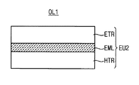
일 실시예에 따르면, 상기 제1 표시 영역에 배치되는 제1 유기 발광층(OL1)과, 상기 제2 표시 영역 또는 상기 제3 표시 영역에 배치되어 상기 투과 영역(TA)에 인접하는 제2 유기 발광층(OL2)은 다른 구성을 가질 수 있다.In an exemplary embodiment, the first organic emission layer OL1 is disposed in the first display area, and the second organic emission layer is disposed in the second display area or the third display area and is adjacent to the transmission area TA. (OL2) may have a different configuration.
예를 들어, 상기 제1 유기 발광층(OL1)은 싱글 발광 구조를 가지고, 상기 제2 유기 발광층(OL2)은 텐덤(tandem) 발광 구조를 가질 수 있다.For example, the first organic emission layer OL1 may have a single emission structure, and the second organic emission layer OL2 may have a tandem emission structure.
도 8을 참조하면, 상기 제1 유기 발광층(OL1)은, 발광층(EML), 전자 수송 영역(ETR) 및 정공 수송 영역(HTR)을 포함할 수 있다. 상기 발광층(EML)은 상기 전자 수송 영역(ETR) 및 상기 정공 수송 영역(HTR) 사이에 배치될 수 있다. 일 실시예에 따르면, 상기 전자 수송 영역(ETR)은 상기 유기 발광 다이오드의 제2 전극(EL2)과 전기적으로 연결될 수 있고, 상기 정공 수송 영역(ETR)은 상기 유기 발광 다이오드의 제1 전극(EL1)과 전기적으로 연결될 수 있다.Referring to FIG. 8 , the first organic emission layer OL1 may include an emission layer EML, an electron transport region ETR, and a hole transport region HTR. The emission layer EML may be disposed between the electron transport region ETR and the hole transport region HTR. According to an embodiment, the electron transport region ETR may be electrically connected to the second electrode EL2 of the organic light emitting diode, and the hole transport region ETR may be electrically connected to the first electrode EL1 of the organic light emitting diode. ) can be electrically connected to.
상기 발광층(EML)은 발광 재료인 호스트를 포함할 수 있다. 예를 들어, 상기 호스트는 Alq3(tris(8-hydroxyquinolino)aluminum), CBP(4,4'-bis(N-carbazolyl)-1,1'-biphenyl), PVK(poly(n-vinylcabazole), ADN(9,10-di(naphthalene-2-yl)anthracene), TCTA(4,4',4''-Tris(carbazol-9-yl)-triphenylamine), TPBi(1,3,5-tris(N-phenylbenzimidazole-2-yl)benzene), TBADN(3-tert-butyl-9,10-di(naphth-2-yl)anthracene), DSA(distyrylarylene), CDBP(4,4′-bis(9-carbazolyl)-2,2′-dimethyl-biphenyl), MADN(2-Methyl-9,10-bis(naphthalen-2-yl)anthracene), DPEPO (bis[2-(diphenylphosphino)phenyl] ether oxide), CP1(Hexaphenyl cyclotriphosphazene), UGH2 (1,4-Bis(triphenylsilyl)benzene), DPSiO3(Hexaphenylcyclotrisiloxane), DPSiO4 (Octaphenylcyclotetra siloxane), PPF (2,8-Bis(diphenylphosphoryl)dibenzofuran) 등을 포함할 수 있다.The light emitting layer EML may include a host that is a light emitting material. For example, the host may be Alq3 (tris(8-hydroxyquinolino)aluminum), CBP(4,4'-bis(N-carbazolyl)-1,1'-biphenyl), PVK(poly(n-vinylcabazole), ADN (9,10-di(naphthalene-2-yl)anthracene), TCTA(4,4',4''-Tris(carbazol-9-yl)-triphenylamine), TPBi(1,3,5-tris(N -phenylbenzimidazole-2-yl)benzene), TBADN(3-tert-butyl-9,10-di(naphth-2-yl)anthracene), DSA(distyrylarylene), CDBP(4,4′-bis(9-carbazolyl) )-2,2′-dimethyl-biphenyl), MADN(2-Methyl-9,10-bis(naphthalen-2-yl)anthracene), DPEPO (bis[2-(diphenylphosphino)phenyl]ether oxide), CP1( Hexaphenyl cyclotriphosphazene), UGH2 (1,4-Bis(triphenylsilyl)benzene), DPSiO3 (Hexaphenylcyclotrisiloxane), DPSiO4 (Octaphenylcyclotetra siloxane), PPF (2,8-Bis(diphenylphosphoryl)dibenzofuran), etc. may be included.
상기 발광층(EML)은, 생성하는 광의 파장에 따라 서로 다른 도펀트를 더 포함할 수 있다. The emission layer EML may further include different dopants depending on the wavelength of the light to be generated.
예를 들어, 상기 발광층(EML)이 적색 광을 생성하는 경우, PtOEP(Pt(II) octaethylporphine), Ir(piq)3 (tris(2-phenylisoquinoline)iridium), Btp2Ir(acac) (bis(2-(2'-benzothienyl)-pyridinato-N,C3')iridium(acetylacetonate) 등을For example, when the light emitting layer (EML) generates red light, PtOEP (Pt(II) octaethylporphine), Ir(piq)3 (tris(2-phenylisoquinoline)iridium), Btp2Ir(acac) (bis(2- (2'-benzothienyl)-pyridinato-N,C3')iridium (acetylacetonate)
적색 도펀트로서 더 포함할 수 있다.It may further include as a red dopant.
예를 들어, 상기 발광층(EML)이 녹색 광을 생성하는 경우, Ir(ppy)3For example, when the emission layer EML generates green light, Ir(ppy)3
(tris(2-phenylpyridine) iridium), Ir(ppy)2(acac) (Bis(2-phenylpyridine)(Acetylacetonato)iridium(III)), Ir(mppy)3(tris(2-(4-tolyl)phenylpiridine)iridium), C545T (10-(2-benzothiazolyl)-1,1,7,7-tetramethyl-2,3,6,7-tetrahydro-1H,5H,11H-[1]benzopyrano [6,7,8-ij]-quinolizin-11-one) 등을 녹색 도펀트로서 더 포함할 수 있다.(tris(2-phenylpyridine) iridium), Ir(ppy)2(acac) (Bis(2-phenylpyridine)(Acetylacetonato)iridium(III)), Ir(mppy)3(tris(2-(4-tolyl)phenylpiridine )iridium), C545T (10-(2-benzothiazolyl)-1,1,7,7-tetramethyl-2,3,6,7-tetrahydro-1H,5H,11H-[1]benzopyrano [6,7,8 -ij]-quinolizin-11-one) and the like may be further included as a green dopant.
예를 들어, 상기 발광층(EML)이 청색 광을 생성하는 경우, (4,6-F2ppy)2Irpic 등을 청색 도펀트로서 더 포함할 수 있다.For example, when the emission layer EML generates blue light, (4,6-F2ppy)2Irpic may be further included as a blue dopant.
상기 정공 수송 영역(HTR)은, 종래에 알려진 다양한 구조를 가질 수 있다. 예를 들어, 상기 정공 수송 영역(HTR)은, 정공 주입층 및 정공 수송층 중 적어도 하나를 포함할 수 있으며, 필요에 따라 정공 버퍼층, 전자 저지층 등을 더 포함할 수 있다. The hole transport region HTR may have various conventionally known structures. For example, the hole transport region HTR may include at least one of a hole injection layer and a hole transport layer, and may further include a hole buffer layer, an electron blocking layer, or the like, if necessary.
일 실시예에 따르면, 상기 정공 수송 영역(HTR)은 상기 제1 전극(EL1)으로부터 차례로 적층된 정공 주입층과 정공 수송층을 포함할 수 있다.According to an embodiment, the hole transport region HTR may include a hole injection layer and a hole transport layer sequentially stacked from the first electrode EL1 .
예를 들어, 상기 정공 주입층은 구리프탈로시아닌(copper phthalocyanine) 등의 프탈로시아닌(phthalocyanine) 화합물, DNTPD(N,N'-diphenyl-N,N'-bis-[4-(phenyl-m-tolyl-amino)-phenyl]-biphenyl-4,4'-diamine), m-MTDATA(4,4',4"-tris(3-methylphenylphenylamino)triphenylamine), TDATA(4,4'4"-Tris(N,N-diphenylamino)triphenylamine), 2TNATA(4,4',4"-tris{N,-(2-naphthyl)-N-phenylamino}-triphenylamine), HATCN(1,4,5,8,9,11-hexaazatriphenylene hexacarbonitrile), PEDOT/PSS(Poly(3,4-ethylenedioxythiophene)/Poly(4-styrenesulfonate)), PANI/DBSA(Polyaniline/Dodecylbenzenesulfonic acid), PANI/CSA(Polyaniline/Camphor sulfonic acid), PANI/PSS((Polyaniline)/Poly(4-styrenesulfonate)) 등을 포함할 수 있다.For example, the hole injection layer may include a phthalocyanine compound such as copper phthalocyanine, N,N'-diphenyl-N,N'-bis-[4-(phenyl-m-tolyl-amino) )-phenyl]-biphenyl-4,4'-diamine), m-MTDATA(4,4',4"-tris(3-methylphenylphenylamino)triphenylamine), TDATA(4,4'4"-Tris(N,N) -diphenylamino)triphenylamine), 2TNATA(4,4',4"-tris{N,-(2-naphthyl)-N-phenylamino}-triphenylamine), HATCN(1,4,5,8,9,11-hexaazatriphenylene hexacarbonitrile), PEDOT/PSS(Poly(3,4-ethylenedioxythiophene)/Poly(4-styrenesulfonate)), PANI/DBSA(Polyaniline/Dodecylbenzenesulfonic acid), PANI/CSA(Polyaniline/Camphor sulfonic acid), PANI/PSS((( Polyaniline)/Poly(4-styrenesulfonate)) and the like.
예를 들어, 상기 정공 수송층은 N-페닐카바졸, 폴리비닐카바졸 등의 카바졸계 유도체, 플루오렌(fluorene)계 유도체, TPD(N,N'-bis(3-methylphenyl)-N,N'-diphenyl-[1,1-biphenyl]-4,4'-diamine), TCTA(4,4',4"-tris(Ncarbazolyl)triphenylamine) 등과 같은 트리페닐아민계 유도체, NPB(N,N'-di(1-naphthyl)-N,N'-diphenylbenzidine), TAPC(4,4'-Cyclohexylidene bis[N,N-bis(4-methylphenyl)benzenamine]) 등을 포함할 수 있다.For example, the hole transport layer may include a carbazole-based derivative such as N-phenylcarbazole or polyvinylcarbazole, a fluorene-based derivative, or TPD (N,N'-bis(3-methylphenyl)-N,N'). Triphenylamine derivatives such as -diphenyl-[1,1-biphenyl]-4,4'-diamine), TCTA(4,4',4"-tris(Ncarbazolyl)triphenylamine), NPB(N,N'- di(1-naphthyl)-N,N'-diphenylbenzidine), TAPC (4,4'-Cyclohexylidene bis[N,N-bis(4-methylphenyl)benzenamine]), and the like.
상기 정공 버퍼층은, 상기 정공 주입층과 상기 정공 수송층 사이에 배치되거나, 상기 정공 수송층과 상기 발광층(EML) 사이에 배치될 수 있다.The hole buffer layer may be disposed between the hole injection layer and the hole transport layer or between the hole transport layer and the light emitting layer EML.
상기 정공 수송 영역은, 위에서 설명된 물질 외에 도전성 향상을 위한 전하 생성 물질을 더 포함할 수 있다. 상기 전하 생성 물질은 상기 정공 수송 영역 내에 균일하게 또는 분균일하게 분산될 수 있다. 예를 들어, 상기 전하 생성 물질은 p-도펀트일 수 있다. 예를 들어, 상기 p-도펀트는 TCNQ(Tetracyanoquinodimethane) 및 F4-TCNQ(2,3,5,6-tetrafluoro-tetracyanoquinodimethane)과 같은 퀴논 유도체, 텅스텐 산화물 및 몰리브덴 산화물과 같은 금속 산화물 등을 포함할 수 있다.The hole transport region may further include a charge generating material for improving conductivity in addition to the materials described above. The charge generating material may be uniformly or uniformly dispersed in the hole transport region. For example, the charge generating material may be a p-dopant. For example, the p-dopant may include quinone derivatives such as TCNQ (Tetracyanoquinodimethane) and F4-TCNQ (2,3,5,6-tetrafluoro-tetracyanoquinodimethane), and metal oxides such as tungsten oxide and molybdenum oxide. .
상기 전자 수송 영역(ETR)은 종래에 알려진 다양한 구조를 가질 수 있다. 예를 들어, 상기 전자 수송 영역(ETR)은, 전자 주입층 및 전자 수송층 중 적어도 하나를 포함할 수 있으며, 필요에 따라 전자 버퍼층, 정공 저지층 등을 더 포함할 수 있다. The electron transport region ETR may have various conventionally known structures. For example, the electron transport region ETR may include at least one of an electron injection layer and an electron transport layer, and may further include an electron buffer layer, a hole blocking layer, or the like, if necessary.
일 실시예에 따르면, 전자 수송 영역(ETR)은 상기 제1 전극(EL1)으로부터 차례로 적층된 전자 수송층과 전자 주입층을 포함할 수 있다.According to an embodiment, the electron transport region ETR may include an electron transport layer and an electron injection layer sequentially stacked from the first electrode EL1 .
예를 들어, 상기 전자 수송층은 Alq3(Tris(8-hydroxyquinolinato)aluminum), TPBi(1,3,5-Tri(1-phenyl-1H-benzo[d]imidazol-2-yl)phenyl), BCP(2,9-Dimethyl-4,7-diphenyl-1,10-phenanthroline), Bphen(4,7-Diphenyl-1,10-phenanthroline), TAZ(3-(4-Biphenylyl)-4-phenyl-5-tert-butylphenyl-1,2,4-triazole), NTAZ(4-(Naphthalen-1-yl)-3,5-diphenyl-4H-1,2,4-triazole), tBu-PBD(2-(4-Biphenylyl)-5-(4-tert-butylphenyl)-1,3,4-oxadiazole), BAlq(Bis(2-methyl-8-quinolinolato-N1,O8)-(1,1'-Biphenyl-4-olato)aluminum), Bebq2(berylliumbis(benzoquinolin-10-olate)), ADN(9,10-di(naphthalene-2-yl)anthracene) 등을 포함할 수 있다.For example, the electron transport layer is Alq3(Tris(8-hydroxyquinolinato)aluminum), TPBi(1,3,5-Tri(1-phenyl-1H-benzo[d]imidazol-2-yl)phenyl), BCP( 2,9-Dimethyl-4,7-diphenyl-1,10-phenanthroline), Bphen(4,7-Diphenyl-1,10-phenanthroline), TAZ(3-(4-Biphenylyl)-4-phenyl-5- tert-butylphenyl-1,2,4-triazole), NTAZ(4-(Naphthalen-1-yl)-3,5-diphenyl-4H-1,2,4-triazole), tBu-PBD(2-(4 -Biphenylyl)-5-(4-tert-butylphenyl)-1,3,4-oxadiazole), BAlq(Bis(2-methyl-8-quinolinolato-N1,O8)-(1,1'-Biphenyl-4- olato)aluminum), Bebq2 (berylliumbis(benzoquinolin-10-olate)), ADN (9,10-di(naphthalene-2-yl)anthracene), and the like.
예를 들어, 상기 전자 주입층은, LiF, LiQ (Lithium quinolate), Li2O,BaO,NaCl,CsF,Yb와 같은 란타넘족 금속, 또는 RbCl, RbI와 같은 할로겐화 금속 등을 포함할 수 있다. For example, the electron injection layer may include a lanthanide metal such as LiF, Lithium quinolate (LiQ), Li 2 O, BaO, NaCl, CsF, Yb, or a metal halide such as RbCl or RbI.
도 9를 참조하면, 상기 제2 유기 발광층(OL2)은, 복수의 발광 구조 유닛을 포함할 수 있다. 예를 들어, 상기 제2 유기 발광층(OL2)은 유기 발광 다이오드의 제1 전극(EL1)에 인접한 제1 발광 구조 유닛(EU1) 및 제2 전극(EL2)에 인접한 제2 발광 구조 유닛(EU2)을 포함할 수 있다.Referring to FIG. 9 , the second organic light emitting layer OL2 may include a plurality of light emitting structure units. For example, the second organic light emitting layer OL2 may include a first light emitting structure unit EU1 adjacent to the first electrode EL1 of the organic light emitting diode and a second light emitting structure unit EU2 adjacent to the second electrode EL2 of the organic light emitting diode. may include.
상기 발광 구조 유닛들은 각각 인가되는 전류에 따라 광을 생성하는 발광층을 포함한다. 예를 들어, 상기 제1 발광 구조 유닛(EU1)은 제1 발광층(EML1), 제1 전자 수송 영역(ETR1) 및 제1 정공 수송 영역(HTR1)을 포함할 수 있다. 상기 제1 발광층(EML1)은 제1 상기 전자 수송 영역(ETR1) 및 상기 제1 정공 수송 영역(HTR1) 사이에 배치될 수 있다. 예를 들어, 상기 제2 발광 구조 유닛(EU2)은 제2 발광층(EML2), 제2 전자 수송 영역(ETR2) 및 제2 정공 수송 영역(HTR2)을 포함할 수 있다. 상기 제2 발광층(EML2)은 제2 상기 전자 수송 영역(ETR2) 및 상기 제2 정공 수송 영역(HTR2) 사이에 배치될 수 있다. Each of the light emitting structure units includes a light emitting layer that generates light according to an applied current. For example, the first light emitting structure unit EU1 may include a first light emitting layer EML1 , a first electron transport region ETR1 , and a first hole transport region HTR1 . The first emission layer EML1 may be disposed between the first electron transport region ETR1 and the first hole transport region HTR1 . For example, the second light emitting structure unit EU2 may include a second light emitting layer EML2 , a second electron transport region ETR2 , and a second hole transport region HTR2 . The second emission layer EML2 may be disposed between the second electron transport region ETR2 and the second hole transport region HTR2 .
상기 제1 정공 수송 영역(HTR1) 및 상기 제2 정공 수송 영역(HTR2)은 각각, 정공 주입층 및 정공 수송층 중 적어도 하나를 포함할 수 있으며, 필요에 따라 정공 버퍼층, 전자 저지층 등을 더 포함할 수 있다. 상기 제1 정공 수송 영역(HTR1) 및 상기 제2 정공 수송 영역(HTR2)은 서로 동일한 구성 또는 다른 구성을 가질 수 있다.Each of the first hole transport region HTR1 and the second hole transport region HTR2 may include at least one of a hole injection layer and a hole transport layer, and further include a hole buffer layer, an electron blocking layer, etc. if necessary. can do. The first hole transport region HTR1 and the second hole transport region HTR2 may have the same configuration or different configurations.
상기 제1 전자 수송 영역(ETR1) 및 상기 제2 전자 수송 영역(ETR2)은 각각, 전자 주입층 및 전자 수송층 중 적어도 하나를 포함할 수 있으며, 필요에 따라 전자 버퍼층, 정공 저지층 등을 더 포함할 수 있다. 상기 제1 전자 수송 영역(ETR1) 및 상기 제2 전자 수송 영역(ETR2)은 서로 동일한 구성 또는 다른 구성을 가질 수 있다.Each of the first electron transport region ETR1 and the second electron transport region ETR2 may include at least one of an electron injection layer and an electron transport layer, and further include an electron buffer layer, a hole blocking layer, etc., if necessary. can do. The first electron transport region ETR1 and the second electron transport region ETR2 may have the same configuration or different configurations.
상기 제1 발광 구조 유닛(EU1)과 상기 제2 발광 구조 유닛(EU2) 사이에는 연결층(CGL)이 배치될 수 있다. A connection layer CGL may be disposed between the first light emitting structure unit EU1 and the second light emitting structure unit EU2 .
예를 들어, 상기 연결층(CGL)은 p 도펀트층 및 n 도펀트층의 적층 구조를 가질 수 있다. 예를 들어, 상기 p 도펀트층은 HAT-CN, TCNQ, NDP-9 등과 같은 p형 도펀트를 포함할 수 있으며, 상기 n 도펀트층은 알칼리 금속, 알칼리 토금속, 란타나이드계 금속 또는 이들의 조합을 포함할 수 있다.For example, the connection layer CGL may have a stacked structure of a p dopant layer and an n dopant layer. For example, the p dopant layer may include a p-type dopant such as HAT-CN, TCNQ, NDP-9, and the like, and the n dopant layer includes an alkali metal, an alkaline earth metal, a lanthanide-based metal, or a combination thereof. can do.
상기 제1 유기 발광층(OL1)과 상기 제2 유기 발광층(OL2)은 진공 증착, 잉크젯 프린팅 등에 의해 형성될 수 있다. 예를 들어, 상기 유기 발광층들은 진공 증착에 의해 형성될 수 있으며, 텐덤 구조를 형성하기 위하여, 미세 금속 마스크(FMM) 등과 같은 마스크를 이용하여 제2 표시 영역 및 제3 표시 영역의 추가 증착을 수행할 수 있다.The first organic emission layer OL1 and the second organic emission layer OL2 may be formed by vacuum deposition, inkjet printing, or the like. For example, the organic emission layers may be formed by vacuum deposition, and additional deposition of the second display area and the third display area is performed using a mask such as a fine metal mask (FMM) to form a tandem structure. can do.
일 실시예에 따르면, 상기 제1 발광층(EML1)과 상기 제2 발광층(EML2)은 같은 색상의 광을 생성할 수 있다. According to an embodiment, the first emission layer EML1 and the second emission layer EML2 may generate light of the same color.
일 실시예에 따르면, 상기 제1 유기 발광층(OL1)을 포함하는 제1 유기 발광 다이오드는 상기 제1 적색 화소 영역(SRA1)에 배치될 수 있으며, 적색 광을 생성할 수 있다. 또한, 상기 제2 유기 발광층(OL2)을 포함하는 제2 유기 발광 다이오드는 상기 제2 적색 화소 영역(SRA2)에 배치될 수 있으며, 적색 광을 생성할 수 있다. According to an embodiment, the first organic light emitting diode including the first organic light emitting layer OL1 may be disposed in the first red pixel area SRA1 and may generate red light. In addition, the second organic light emitting diode including the second organic light emitting layer OL2 may be disposed in the second red pixel area SRA2 and may generate red light.
상기 제2 유기 발광층(OL2)은 셋 이상의 발광 구조 유닛들을 포함할 수도 있다.The second organic light emitting layer OL2 may include three or more light emitting structure units.
예를 들어, 도 10에 도시된 것과 같이, 상기 제2 유기 발광층(OL2)은 제1 발광 구조 유닛(EU1), 제2 발광 구조 유닛(EU2) 및 제3 발광 구조 유닛(EU3)을 포함할 수 있다.For example, as shown in FIG. 10 , the second organic light emitting layer OL2 may include a first light emitting structure unit EU1 , a second light emitting structure unit EU2 , and a third light emitting structure unit EU3 . can
상기 발광 구조 유닛들은 각각 인가되는 전류에 따라 광을 생성하는 발광층을 포함한다. 예를 들어, 상기 제1 발광 구조 유닛(EU1)은 제1 발광층(EML1), 제1 전자 수송 영역(ETR1) 및 제1 정공 수송 영역(HTR1)을 포함할 수 있다. 상기 제1 발광층(EML1)은 제1 상기 전자 수송 영역(ETR1) 및 상기 제1 정공 수송 영역(HTR1) 사이에 배치될 수 있다. 상기 제2 발광 구조 유닛(EU2)은 제2 발광층(EML2), 제2 전자 수송 영역(ETR2) 및 제2 정공 수송 영역(HTR2)을 포함할 수 있다. 상기 제2 발광층(EML2)은 제2 상기 전자 수송 영역(ETR2) 및 상기 제2 정공 수송 영역(HTR2) 사이에 배치될 수 있다. 상기 제3 발광 구조 유닛(EU3)은 제3 발광층(EML3), 제3 전자 수송 영역(ETR3) 및 제3 정공 수송 영역(HTR3)을 포함할 수 있다. 상기 제3 발광층(EML3)은 제3 상기 전자 수송 영역(ETR3) 및 상기 제3 정공 수송 영역(HTR3) 사이에 배치될 수 있다. Each of the light emitting structure units includes a light emitting layer that generates light according to an applied current. For example, the first light emitting structure unit EU1 may include a first light emitting layer EML1 , a first electron transport region ETR1 , and a first hole transport region HTR1 . The first emission layer EML1 may be disposed between the first electron transport region ETR1 and the first hole transport region HTR1 . The second light emitting structure unit EU2 may include a second light emitting layer EML2 , a second electron transport region ETR2 , and a second hole transport region HTR2 . The second emission layer EML2 may be disposed between the second electron transport region ETR2 and the second hole transport region HTR2 . The third light emitting structure unit EU3 may include a third light emitting layer EML3 , a third electron transport region ETR3 , and a third hole transport region HTR3 . The third emission layer EML3 may be disposed between the third electron transport region ETR3 and the third hole transport region HTR3 .
상기 제1 정공 수송 영역(HTR1), 상기 제2 정공 수송 영역(HTR2) 및 제3 정공 수송 영역(HTR3)은 각각, 정공 주입층 및 정공 수송층 중 적어도 하나를 포함할 수 있으며, 필요에 따라 정공 버퍼층, 전자 저지층 등을 더 포함할 수 있다. 상기 제1 정공 수송 영역(HTR1), 상기 제2 정공 수송 영역(HTR2) 및 제3 정공 수송 영역(HTR3)은 서로 동일한 구성 또는 다른 구성을 가질 수 있다.Each of the first hole transport region HTR1 , the second hole transport region HTR2 , and the third hole transport region HTR3 may include at least one of a hole injection layer and a hole transport layer. It may further include a buffer layer, an electron blocking layer, and the like. The first hole transport region HTR1 , the second hole transport region HTR2 , and the third hole transport region HTR3 may have the same configuration or different configurations.
상기 제1 전자 수송 영역(ETR1), 상기 제2 전자 수송 영역(ETR2) 및 상기 제3 전자 수송 영역(ETR3)은 각각, 전자 주입층 및 전자 수송층 중 적어도 하나를 포함할 수 있으며, 필요에 따라 전자 버퍼층, 정공 저지층 등을 더 포함할 수 있다. 상기 제1 전자 수송 영역(ETR1), 상기 제2 전자 수송 영역(ETR2) 및 상기 제3 전자 수송 영역(ETR3)은 서로 동일한 구성 또는 다른 구성을 가질 수 있다.Each of the first electron transport region ETR1 , the second electron transport region ETR2 , and the third electron transport region ETR3 may include at least one of an electron injection layer and an electron transport layer. It may further include an electron buffer layer, a hole blocking layer, and the like. The first electron transport region ETR1 , the second electron transport region ETR2 , and the third electron transport region ETR3 may have the same configuration or different configurations.
상기 제1 발광 구조 유닛(EU1)과 상기 제2 발광 구조 유닛(EU2) 사이에는 제1 연결층(CGL1)이 배치될 수 있다. 상기 제2 발광 구조 유닛(EU2)과 상기 제3 발광 구조 유닛(EU3) 사이에는 제2 연결층(CGL2)이 배치될 수 있다. A first connection layer CGL1 may be disposed between the first light emitting structure unit EU1 and the second light emitting structure unit EU2 . A second connection layer CGL2 may be disposed between the second light emitting structure unit EU2 and the third light emitting structure unit EU3 .
일 실시예에 따른 표시 장치는, 제2 표시 영역(DA2)에서 투과 영역(TA)에 의해 휘도가 감소될 수 있다. 이러한 감소된 휘도를 보상하기 위하여 구동 전류를 부분적으로 증가시키는 방법이 고려될 수 있다. 그러나, 표시 영역 전체에서 유기 발광 다이오드들이 동일한 발광 구조를 갖는 표시 장치에서 구동 전류가 부분적으로 증가되면, 해당 영역의 유기 발광 다이오드들의 수명이 감소하여, 전체 표시 패널의 내구성 및 신뢰성이 저하될 수 있다.In the display device according to an exemplary embodiment, luminance may be reduced by the transmissive area TA in the second display area DA2 . A method of partially increasing the driving current to compensate for this reduced luminance may be considered. However, when the driving current is partially increased in a display device having the same light emitting structure as the organic light emitting diodes in the entire display area, the lifespan of the organic light emitting diodes in the corresponding area may decrease, thereby reducing durability and reliability of the entire display panel. .
일 실시예에 따르면, 상기 제2 유기 발광층(OL2)은 복수의 발광 구조 유닛을 포함함에 따라, 싱글 발광 구조 유닛을 포함하는 제1 유기 발광층(OL1) 보다 높은 휘도의 광을 생성할 수 있다. 또한, 휘도 증가를 위하여 구동 전류가 증가되더라도 텐덤 구조에 의해 부분적 열화가 방지될 수 있다.According to an embodiment, since the second organic light emitting layer OL2 includes a plurality of light emitting structure units, light having a higher luminance than that of the first organic light emitting layer OL1 including a single light emitting structure unit may be generated. In addition, even if the driving current is increased to increase the luminance, partial deterioration may be prevented by the tandem structure.
상기 제2 유기 발광 다이오드의 휘도를 증가시키면서 전력 효율 감소를 최소화하기 위하여, 상기 제2 표시 영역(DA2)에 전원을 제공하는 전원 배선은 상기 제1 표시 영역(DA1)에 전원을 제공하는 전원 배선과 분리되는 것이 바람직할 수 있다. In order to minimize a decrease in power efficiency while increasing the luminance of the second organic light emitting diode, a power line providing power to the second display area DA2 is a power line providing power to the first display area DA1 . It may be desirable to separate from
예를 들어, 상기 표시 장치는, 상기 제1 표시 영역(DA1)에 정전압을 전달하는 제1 전원 배선과 상기 제2 표시 영역(DA2)에 정전압을 전달하는 제2 전원 배선을 포함할 수 있으며, 상기 제1 전원 배선과 상기 제2 전원 배선에는 서로 다른 크기의 정전압이 인가될 수 있다. 상기 제1 표시 영역(DA1)에 배치되는 제1 구동 소자는 상기 제1 전원 배선과 전기적으로 연결되어, 상기 제1 유기 발광 다이오드에 제1 전원 전압을 제공할 수 있고, 상기 제2 표시 영역(DA2)에 배치되는 제2 구동 소자는 상기 제2 전원 배선과 전기적으로 연결되어, 상기 제2 유기 발광 다이오드에 제2 전원 전압을 제공할 수 있다.For example, the display device may include a first power line transmitting a constant voltage to the first display area DA1 and a second power line transmitting a constant voltage to the second display area DA2, Different magnitudes of constant voltages may be applied to the first power line and the second power line. A first driving element disposed in the first display area DA1 may be electrically connected to the first power line to provide a first power voltage to the first organic light emitting diode, and may be provided in the second display area ( The second driving element disposed on DA2) may be electrically connected to the second power line to provide a second power voltage to the second organic light emitting diode.
일 실시예에서, 상기 제3 표시 영역(DA3)은 위에서 설명된 제2 표시 영역(DA2)의 구성과 동일 내지 유사한 구성을 가질 수 있다.In an embodiment, the third display area DA3 may have the same or similar configuration to that of the second display area DA2 described above.
일 실시예에서, 상기 제1 유기 발광 다이오드는 싱글 발광 구조 유닛을 포함하는 것으로 예시하였으나, 본 발명의 실시예들은 이에 한정되지 않는다.In one embodiment, the first organic light emitting diode has been exemplified as including a single light emitting structure unit, but embodiments of the present invention are not limited thereto.
예를 들어, 상기 제1 유기 발광 다이오드 및 상기 제2 유기 발광 다이오드는 서로 다른 텐덤 구조를 가질 수 있다.For example, the first organic light emitting diode and the second organic light emitting diode may have different tandem structures.
예를 들어, 상기 제1 유기 발광 다이오드는 도 9에 도시된 것과 같이 2개의 발광 구조 유닛을 포함하고, 상기 제2 유기 발광 다이오드는 도 10에 도시된 것과 같이 3개의 발광 구조 유닛을 포함할 수 있다.For example, the first organic light emitting diode may include two light emitting structure units as shown in FIG. 9 , and the second organic light emitting diode may include three light emitting structure units as shown in FIG. 10 . have.
다른 실시예에서, 상기 제1 표시 영역(DA1)에 배치되는 제1 유기 발광 다이오드는 싱글 발광 구조 유닛을 포함하고, 상기 제2 표시 영역(DA2)에 배치되는 제2 유기 발광 다이오드는 2개의 발광 구조 유닛을 포함하고, 상기 제3 표시 영역(DA3)에 배치되는 제3 유기 발광 다이오드는 3개의 발광 구조 유닛을 포함할 수 있다.In another embodiment, the first organic light emitting diode disposed in the first display area DA1 includes a single light emitting structure unit, and the second organic light emitting diode disposed in the second display area DA2 includes two light emitting diodes. The third organic light emitting diode may include a structure unit, and the third organic light emitting diode disposed in the third display area DA3 may include three light emitting structure units.
일 실시예에 따르면, 상기 텐덤 구조는 상기 제2 표시 영역(DA2) 내에 배치되는 유기 발광 다이오드 전체에 적용될 수 있다. 그러나, 본 발명의 실시예들은 이에 한정되지 않는다. 예를 들어, 상기 텐덤 구조는 상기 제2 표시 영역(DA2) 내에서 선택적으로 적용될 수 있다. 일 실시예에 따르면, 상기 제2 청색 화소 영역(SBA2)에 배치되는 유기 발광 다이오드는 복수의 발광 구조 유닛을 포함하고, 상기 제2 적색 화소 영역(SRA2) 및 상기 제2 녹색 화소 영역(SGA2)에 배치되는 발광 다이오드는 싱글 발광 구조 유닛을 포함하거나, 상기 제2 청색 화소 영역(SBA2)에 배치되는 유기 발광 다이오드 보다 적은 수의 발광 구조 유닛을 포함할 수 있다.According to an embodiment, the tandem structure may be applied to the entire organic light emitting diode disposed in the second display area DA2. However, embodiments of the present invention are not limited thereto. For example, the tandem structure may be selectively applied in the second display area DA2 . According to an exemplary embodiment, the organic light emitting diode disposed in the second blue pixel area SBA2 includes a plurality of light emitting structure units, and the second red pixel area SRA2 and the second green pixel area SGA2 are provided. The light emitting diodes disposed in the light emitting diode may include a single light emitting structure unit or may include a smaller number of light emitting structure units than the organic light emitting diodes disposed in the second blue pixel area SBA2.
위와 같은 구성은, 발광 효율이 가작 낮은 청색 화소 영역의 휘도를 선택적으로 증가시킴으로써, 소비 전력 증가를 최소화하면서 제2 표시 영역의 휘도 감소를 효율적으로 보상할 수 있다.In the above configuration, by selectively increasing the luminance of the blue pixel region having the lowest luminous efficiency, it is possible to efficiently compensate for the decrease in luminance of the second display region while minimizing the increase in power consumption.
본 발명의 일 실시예에 따르면, 제1 표시 영역(DA1)에 배치되는 제1 유기 발광층(OL1)과 제2 표시 영역(DA2)에 배치되는 제2 유기 발광층(OL2)은 서로 다른 물질을 포함할 수 있다. 예를 들어, 상기 제2 유기 발광층(OL2)은, 상기 제1 유기 발광층(OL1)의 발광 물질 보다 발광 효율이 높은 발광 물질을 포함할 수 있다. According to an exemplary embodiment, the first organic emission layer OL1 disposed in the first display area DA1 and the second organic emission layer OL2 disposed in the second display area DA2 include different materials. can do. For example, the second organic light emitting layer OL2 may include a light emitting material having a higher luminous efficiency than the light emitting material of the first organic light emitting layer OL1 .
일 실시예에 따르면, 상기 제1 유기 발광층(OL1)은 형광 도펀트를 포함하고, 상기 제2 유기 발광층(OL2)은 인광 도펀트를 포함할 수 있다. 일 실시예에 따르면, 상기 제1 유기 발광층(OL1)은 인광 도펀트를 포함하고, 상기 제2 유기 발광층(OL2)은 열활성 지연 형광 (thermally activated delayed fluorescence, TADF) 도펀트를 포함할 수 있다. 일 실시예에 따르면, 상기 제1 유기 발광층(OL1)은 형광 도펀트를 포함하고, 상기 제2 유기 발광층(OL2)은 TADF 도펀트를 포함할 수 있다.According to an embodiment, the first organic emission layer OL1 may include a fluorescent dopant, and the second organic emission layer OL2 may include a phosphorescent dopant. According to an embodiment, the first organic emission layer OL1 may include a phosphorescent dopant, and the second organic emission layer OL2 may include a thermally activated delayed fluorescence (TADF) dopant. According to an embodiment, the first organic emission layer OL1 may include a fluorescent dopant, and the second organic emission layer OL2 may include a TADF dopant.
예를 들어, 상기 형광 도펀트는 페릴렌(perylene), TBPe(2,5,8,11-tetra-tert-butylperylene), BCzVB(1,4-bis[2-(3-N-ethylcarbazoryl)vinyl]benzene), BCzVBi(4,4'-bis(9-ethyl-3-carbazovinylene)-1,1'-biphenyl), BDAVBi(4,4'-bis[4-diphenylamino]styryl)biphenyl), DPAVB(4-(di-p-tolylamino)-4'-[(di-ptolylamino)styryl]stilbene), DPAVBi(4,4'-bis[4-(di-p-tolylamino)styryl]bipnehyl), DSA-Ph(1-4-di-[4-(N,N-diphenyl)amino]styryl-benzene), Coumarin 6, C545T, DMQA(N,N'-dimethyl-quinacridone), DBQA(5,12-Dibutylquinacridone), TTPA(9,10-bis[N,N-di-(p-tolyl)-amino]anthracene), TPA(9,10-bis[phenyl(m-tolyl)-amino]anthracene), BA-TTB, BATAB, BA-NPB, DEQ(N,N'-diethylquinacridone), DCM(4-(dicyanomethylene)-2-methyl-6-[p-(dimethylamino)styryl]-4H-pyran), DCM2(4-(dicyanomethylene)-2-methyl-6-julolidyl-9-enyl-4H-pyran), DCJT(4-(dicyanomethylene)-2-methyl-6-(1,1,7,7-tetramethyljulolidyl-9-enyl)-4H-pyran), DCJTB (4-(Dicyanomethylene)-2-tert-butyl-6-(1,1,7,7,-tetramethyljulolidyl-9-enyl)-4Hpyran), DCJTI, DCJMTB, DPP(6,13-diphenylpentacene), DCDDC(3-(dicyanomethylene)-5,5-dimethyl-1-[(4-dimethylamino)styryl]cyclohexene), AAAP(6-methyl-3-[3-(1,1,6,6-tetramethyl-10-oxo-2,3,5,6-tetrahydro-1H,4H,10H-11-oxa-3a-azabenzo[de]-anthracen-9-yl)acryloyl]pyran-2,4-dione), (PPA)(PSA)Pe-1(3-(N-phenyl-N-p-tolylamino)-9-(N-p-styrylphenyl-N-p-tolylamino)perylene), BSN(1,10-dicyano-substituted bisstyrylnaphthalene derivative), DBP(tetraphenyldibenzoperiflanthene), TBRb(2,8-di-tert-butyl-5,11-bis(4-tert-butylphenyl)-6,12-diphenyltetracene), 루브렌(rubrene) 등을 포함할 수 있다.For example, the fluorescent dopant is perylene (perylene), TBPe (2,5,8,11-tetra-tert-butylperylene), BCzVB (1,4-bis[2-(3-N-ethylcarbazoryl)vinyl] benzene), BCzVBi(4,4'-bis(9-ethyl-3-carbazovinylene)-1,1'-biphenyl), BDAVBi(4,4'-bis[4-diphenylamino]styryl)biphenyl), DPAVB(4 -(di-p-tolylamino)-4'-[(di-ptolylamino)styryl]stilbene), DPAVBi(4,4'-bis[4-(di-p-tolylamino)styryl]bipnehyl), DSA-Ph( 1-4-di-[4-(N,N-diphenyl)amino]styryl-benzene), Coumarin 6, C545T, DMQA(N,N'-dimethyl-quinacridone), DBQA(5,12-Dibutylquinacridone), TTPA (9,10-bis[N,N-di-(p-tolyl)-amino]anthracene), TPA(9,10-bis[phenyl(m-tolyl)-amino]anthracene), BA-TTB, BATAB, BA-NPB, DEQ(N,N'-diethylquinacridone), DCM(4-(dicyanomethylene)-2-methyl-6-[p-(dimethylamino)styryl]-4H-pyran), DCM2(4-(dicyanomethylene)- 2-methyl-6-julolidyl-9-enyl-4H-pyran), DCJT(4-(dicyanomethylene)-2-methyl-6-(1,1,7,7-tetramethyljulolidyl-9-enyl)-4H-pyran ), DCJTB (4-(Dicyanomethylene)-2-tert-butyl-6-(1,1,7,7,-tetramethyljulolidyl-9-enyl)-4Hpyran), DCJTI, DCJMTB, DPP(6,13-diphenylpentacen) e), DCDDC (3-(dicyanomethylene)-5,5-dimethyl-1-[(4-dimethylamino)styryl]cyclohexene), AAAP (6-methyl-3-[3-(1,1,6,6- tetramethyl-10-oxo-2,3,5,6-tetrahydro-1H,4H,10H-11-oxa-3a-azabenzo[de]-anthracen-9-yl)acryloyl]pyran-2,4-dione), (PPA)(PSA)Pe-1(3-(N-phenyl-Np-tolylamino)-9-(Np-styrylphenyl-Np-tolylamino)perylene), BSN(1,10-dicyano-substituted bisstyrylnaphthalene derivative), DBP (tetraphenyldibenzoperiflanthene), TBRb (2,8-di-tert-butyl-5,11-bis(4-tert-butylphenyl)-6,12-diphenyltetracene), and rubrene.
상기 인광 도펀트는 전이금속의 착체(complex)일 수 있다. 상기 전이금속의 착체는 예를 들어 이리듐(Ir), 백금(Pt), 오스뮴(Os), 백금(Au), 티탄(Ti), 지르코늄(Zr), 하프늄(Hf), 유로퓸(Eu), 테르븀(Tb) 또는 툴륨(Tm)의 착체일 수 있다. 예를 들어, 상기 인광 도펀트는 앞서 설명된 적색 도펀트, 녹색 도펀트 및 청색 도펀트로 예시될 수 있다.The phosphorescent dopant may be a complex of a transition metal. The complex of the transition metal is, for example, iridium (Ir), platinum (Pt), osmium (Os), platinum (Au), titanium (Ti), zirconium (Zr), hafnium (Hf), europium (Eu), terbium (Tb) or a complex of thulium (Tm). For example, the phosphorescent dopant may be exemplified by the above-described red dopant, green dopant, and blue dopant.
예를 들어, 상기 TADF 도펀트는, 헤테로시클릭 화합물을 포함할 수 있다. 예를 들어, 상기 헤테로시클릭 화합물은 산화된 티아디아졸계 코어를 가질 수 있다.For example, the TADF dopant may include a heterocyclic compound. For example, the heterocyclic compound may have an oxidized thiadiazole-based core.
상기의 발광 효율이 다른 도펀트들의 조합은, 유기 발광 다이오드가 생성하는 광의 파장에 따라 달라질 수 있다.A combination of dopants having different luminous efficiencies may vary depending on the wavelength of light generated by the organic light emitting diode.
일 실시예에 따르면, 상기 제1 표시 영역(DA1)에 배치되는 제1 녹색 화소 영역(SGA1)은 형광 도펀트를 포함하고, 상기 제2 표시 영역(DA2)에 배치되는 제2 녹색 화소 영역(SGA2)은 인광 도펀트를 포함할 수 있다. 상기 제1 표시 영역(DA1)에 배치되는 제1 적색 화소 영역(SRA1)은 인광 도펀트를 포함하고, 상기 제2 표시 영역(DA2)에 배치되는 제2 적색 화소 영역(SRA2)은 TADF 도펀트를 포함할 수 있다. 상기 제1 표시 영역(DA1)에 배치되는 제1 청색 화소 영역(SBA1)은 형광 도펀트를 포함하고, 상기 제2 표시 영역(DA2)에 배치되는 제2 청색 화소 영역(SBA2)은 인광 도펀트를 포함할 수 있다.According to an exemplary embodiment, the first green pixel area SGA1 disposed in the first display area DA1 includes a fluorescent dopant, and the second green pixel area SGA2 disposed in the second display area DA2. ) may include a phosphorescent dopant. The first red pixel area SRA1 disposed in the first display area DA1 includes a phosphorescent dopant, and the second red pixel area SRA2 disposed in the second display area DA2 includes a TADF dopant. can do. The first blue pixel area SBA1 disposed in the first display area DA1 includes a fluorescent dopant, and the second blue pixel area SBA2 disposed in the second display area DA2 includes a phosphorescent dopant. can do.
상기의 구성에서, 도펀트 분율을 적절하게 조절함으로써 색좌표 변화를 제어할 수 있다. In the above configuration, the color coordinate change can be controlled by appropriately adjusting the dopant fraction.
일 실시예에서, 상기 제3 표시 영역(DA3)은 위에서 설명된 제2 표시 영역(DA2)의 구성과 동일 내지 유사한 구성을 가질 수 있다.In an embodiment, the third display area DA3 may have the same or similar configuration to that of the second display area DA2 described above.
본 발명의 실시예들에 따른 표시 장치에서, 표시 영역은 다양한 형상과 배치를 가질 수 있다. 도 11 내지 도 13은 본 발명의 일 실시예에 따른 표시 장치를 도시한 평면도들이다. In the display device according to the exemplary embodiment of the present invention, the display area may have various shapes and arrangements. 11 to 13 are plan views illustrating a display device according to an exemplary embodiment.
도 11을 참조하면, 표시 장치(20)는 제1 표시 영역(DA1), 상기 제1 표시 영역(DA1) 보다 큰 단위 면적당 투과율을 갖는 제2 표시 영역(DA2) 및 상기 제2 표시 영역(DA2) 보다 큰 단위 면적당 투과율을 갖는 제3 표시 영역(DA3)을 포함한다. 상기 제2 표시 영역(DA2)은 상기 제1 표시 영역(DA1)과 제1 방향(D1)을 따라 인접하고, 상기 제1 방향(D1)과 수직하는 제2 방향(D2)을 따라 연장되는 형상을 가질 수 있다. 또한, 상기 제2 표시 영역(DA2)은, 홀 형상의 제3 표시 영역(DA3)을 둘러싸는 형상을 가질 수 있다. Referring to FIG. 11 , the
도 12를 참조하면, 표시 장치(30)는 제1 표시 영역(DA1), 상기 제1 표시 영역(DA1) 보다 큰 단위 면적당 투과율을 갖는 제2 표시 영역(DA2) 및 상기 제2 표시 영역(DA2) 보다 큰 단위 면적당 투과율을 갖는 제3 표시 영역(DA3)을 포함한다. 상기 제2 표시 영역(DA2)은 제1 방향(D1)과 수직하는 제2 방향(D2)을 따라 연장되는 형상을 가질 수 있으며, 상기 제1 표시 영역(DA1) 내에 배치될 수 있다. 또한, 홀 형상의 제3 표시 영역(DA3)과 이격될 수 있다.Referring to FIG. 12 , the
도 13을 참조하면, 표시 장치(40)는 제1 표시 영역(DA1) 및 상기 제1 표시 영역(DA1) 보다 큰 단위 면적당 투과율을 갖는 제2 표시 영역(DA2)을 포함한다. 상기 제2 표시 영역(DA2)은 센서 모듈과 중첩할 수 있다. Referring to FIG. 13 , the
일 실시예에 따르면, 상기 표시 장치(40)는 비표시 영역(NA)을 더 포함할 수 있다. 예를 들어, 상기 비표시 영역(NA)은 상기 표시 영역에 의해 둘러싸여지거나, 상기 표시 영역의 안쪽으로 함입된 형상을 가질 수 있다. 상기 비표시 영역(NA)은 영상을 표시하지 않는다. 또한, 상기 비표시 영역(NA)의 투과율을 높이기 위하여, 상기 비표시 영역(NA)에서는 발광 소자를 포함하는 발광 구조물, 도전성 배선을 포함하는 회로 구조물, 절연 구조물, 봉지층 및 베이스 기판 중 적어도 하나가 제거될 수 있으며, 이들 전체가 제거되어 홀을 형성할 수도 있다.According to an embodiment, the
상기 표시 장치(40)는 상기 비표시 영역(NA)과 중첩하는 카메라 모듈을 포함할 수 있다. 상기 카메라 모듈은 표시 패널 하부에 배치될 수 있다. 다른 실시예에서, 상기 카메라 모듈의 일부는 상기 비표시 영역(NA)에 대응되는 홀에 삽입될 수 있다.The
일 실시예에 따르면, 카메라 모듈이 입사하는 광량을 증가사키기 위하여, 상기 표시 장치는 비표시 영역을 포함할 수 있다.According to an embodiment, the display device may include a non-display area in order to increase the amount of light incident to the camera module.
본 발명의 실시예들은 투과 영역을 갖는 다양한 표시 장치에 적용될 수 있다. 예를 들어, 일 실시예에 따른 표시 장치에 있어서, 큰 단위 면적당 투과율을 갖는 제2 표시 영역은 기능성 모듈과 중첩하지 않을 수 있다. 이에 따라, 부분적으로 투과 영역을 갖는 투명 디스플레이를 구현할 수 있다.Embodiments of the present invention may be applied to various display devices having a transmissive region. For example, in the display device according to an embodiment, the second display area having a large transmittance per unit area may not overlap the functional module. Accordingly, it is possible to implement a transparent display having a partially transparent area.
상술한 바에서는, 본 발명의 예시적인 실시예들을 참조하여 설명하였지만, 해당 기술 분야에서 통상의 지식을 가진 자라면 하기의 특허청구범위에 기재된 본 발명의 사상 및 영역으로부터 벗어나지 않는 범위 내에서 본 발명을 다양하게 수정 및 변경시킬 수 있음을 이해할 것이다.In the foregoing, although the description has been made with reference to exemplary embodiments of the present invention, those skilled in the art will present the present invention within the scope not departing from the spirit and scope of the present invention described in the claims below. It will be understood that various modifications and variations are possible.
본 발명은 다양한 표시 장치들에 적용될 수 있다. 예를 들면, 본 발명은 차량용, 선박용 및 항공기용 디스플레이 장치들, 휴대용 통신 장치들, 전시용 또는 정보 전달용 디스플레이 장치들, 의료용 디스플레이 장치들 등과 같은 다양한 디스플레이 기기들에 적용 가능하다.The present invention can be applied to various display devices. For example, the present invention is applicable to various display devices such as display devices for vehicles, ships and aircraft, portable communication devices, display devices for exhibition or information transmission, medical display devices, and the like.
Claims (20)
상기 표시 패널은, 상기 제1 표시 영역 및 상기 제2 표시 영역에 배치되는 복수의 유기 발광 다이오드들을 포함하고,
상기 제2 표시 영역에 배치되는 제2 유기 발광 다이오드는, 상기 제1 표시 영역에 배치되는 제1 유기 발광 다이오드보다 많은 발광 구조 유닛들을 포함하는, 유기 발광 표시 장치.A display panel comprising: a display panel including a first display area and a second display area having a transmittance per unit area different from that of the first display area;
the display panel includes a plurality of organic light emitting diodes disposed in the first display area and the second display area;
The second organic light emitting diode disposed in the second display area includes more light emitting structure units than the first organic light emitting diode disposed in the first display area.
상기 제1 유기 발광 다이오드에 제1 전원 전압을 제공하는 제1 구동 소자;
상기 제2 유기 발광 다이오드에 제2 전원 전압을 제공하는 제2 구동 소자; 및
상기 제1 구동 소자 및 상기 제2 구동 소자에 전원 전압을 전달하는 전원 배선들을 더 포함하고,
상기 제1 구동 소자와 연결되는 제1 전원 배선과 상기 제2 구동 소자와 연결되는 제2 전원 배선에는 서로 다른 정전압이 인가되는 것을 특징으로 하는 유기 발광 표시 장치.The method of claim 1 , wherein the display panel comprises:
a first driving element providing a first power voltage to the first organic light emitting diode;
a second driving element providing a second power voltage to the second organic light emitting diode; and
Further comprising power lines for transferring a power voltage to the first driving element and the second driving element,
The organic light emitting diode display device, wherein different constant voltages are applied to a first power line connected to the first driving element and a second power line connected to the second driving element.
상기 표시 패널은, 상기 제1 표시 영역 및 상기 제2 표시 영역에 배치되는 복수의 유기 발광 다이오드들을 포함하고,
상기 제2 표시 영역에 배치되는 제2 유기 발광 다이오드의 발광층은, 상기 제1 표시 영역에 배치되는 제1 유기 발광 다이오드의 발광층과 다른 재료 구성을 갖는, 유기 발광 표시 장치.A display panel comprising: a display panel including a first display area and a second display area having a transmittance per unit area different from that of the first display area;
the display panel includes a plurality of organic light emitting diodes disposed in the first display area and the second display area;
The light emitting layer of the second organic light emitting diode disposed in the second display area has a material configuration different from that of the light emitting layer of the first organic light emitting diode disposed in the first display area.
The organic light emitting diode display of claim 13 , further comprising: a sensor module overlapping the second display area and a camera module overlapping the third display area.
Priority Applications (4)
| Application Number | Priority Date | Filing Date | Title |
|---|---|---|---|
| KR1020200018185A KR20210104201A (en) | 2020-02-14 | 2020-02-14 | Organic light-emitting display device |
| US17/162,106 US12207516B2 (en) | 2020-02-14 | 2021-01-29 | Organic light-emitting display device |
| CN202110187999.5A CN113270554A (en) | 2020-02-14 | 2021-02-09 | Organic light emitting display device |
| US19/029,051 US20250169319A1 (en) | 2020-02-14 | 2025-01-17 | Organic light-emitting display device |
Applications Claiming Priority (1)
| Application Number | Priority Date | Filing Date | Title |
|---|---|---|---|
| KR1020200018185A KR20210104201A (en) | 2020-02-14 | 2020-02-14 | Organic light-emitting display device |
Publications (1)
| Publication Number | Publication Date |
|---|---|
| KR20210104201A true KR20210104201A (en) | 2021-08-25 |
Family
ID=77228136
Family Applications (1)
| Application Number | Title | Priority Date | Filing Date |
|---|---|---|---|
| KR1020200018185A Pending KR20210104201A (en) | 2020-02-14 | 2020-02-14 | Organic light-emitting display device |
Country Status (3)
| Country | Link |
|---|---|
| US (2) | US12207516B2 (en) |
| KR (1) | KR20210104201A (en) |
| CN (1) | CN113270554A (en) |
Families Citing this family (8)
| Publication number | Priority date | Publication date | Assignee | Title |
|---|---|---|---|---|
| KR102818817B1 (en) | 2019-08-09 | 2025-06-11 | 오티아이 루미오닉스 인크. | Optoelectronic device including auxiliary electrode and partition |
| CN111508416B (en) * | 2020-04-30 | 2021-09-03 | 武汉华星光电半导体显示技术有限公司 | Display and driving method thereof |
| WO2022123431A1 (en) | 2020-12-07 | 2022-06-16 | Oti Lumionics Inc. | Patterning a conductive deposited layer using a nucleation inhibiting coating and an underlying metallic coating |
| DE102021132877A1 (en) | 2020-12-30 | 2022-06-30 | Lg Display Co., Ltd. | DISPLAY BOARD AND DISPLAY DEVICE |
| CN113328044B (en) * | 2021-05-25 | 2023-04-18 | 武汉华星光电技术有限公司 | Display panel, preparation method thereof and display device |
| CN115188788A (en) * | 2022-06-29 | 2022-10-14 | 武汉天马微电子有限公司 | Display panel and display device |
| CN115000319B (en) * | 2022-07-29 | 2022-12-06 | 京东方科技集团股份有限公司 | Display panel, manufacturing method thereof, and light emitting device |
| KR20250103191A (en) * | 2023-12-28 | 2025-07-07 | 엘지디스플레이 주식회사 | Display device |
Family Cites Families (29)
| Publication number | Priority date | Publication date | Assignee | Title |
|---|---|---|---|---|
| KR20080071415A (en) * | 2007-01-30 | 2008-08-04 | 삼성에스디아이 주식회사 | Plasma Display Panel with Nanoporous Carbon Particle Layer |
| US20100141126A1 (en) * | 2007-05-16 | 2010-06-10 | Konica Minolta Holdings, Inc. | Organic electroluminescent element, display and illuminating device |
| JP2009004711A (en) | 2007-06-25 | 2009-01-08 | Canon Inc | Measuring apparatus, exposure apparatus, and device manufacturing method |
| KR101351410B1 (en) | 2009-09-29 | 2014-01-14 | 엘지디스플레이 주식회사 | White Organic Light Emitting Device |
| CN102790181A (en) * | 2011-05-18 | 2012-11-21 | 海洋王照明科技股份有限公司 | Lamination transmission type white organic electroluminescent device |
| WO2013051234A1 (en) * | 2011-10-04 | 2013-04-11 | ソニー株式会社 | Organic electroluminescent element |
| US9437132B2 (en) | 2011-11-30 | 2016-09-06 | Apple Inc. | Devices and methods for providing access to internal component |
| KR101429924B1 (en) | 2011-12-08 | 2014-08-14 | 엘지디스플레이 주식회사 | Tandem White Organic Emitting Device |
| KR101275810B1 (en) * | 2012-01-20 | 2013-06-18 | 삼성디스플레이 주식회사 | Organic light emitting display device |
| KR20140092119A (en) | 2013-01-15 | 2014-07-23 | 삼성디스플레이 주식회사 | Flat panel display device |
| KR20150043605A (en) * | 2013-10-11 | 2015-04-23 | 삼성디스플레이 주식회사 | Organic light emitting diode and method of cutting organic light emitting diode display panel |
| KR102232533B1 (en) * | 2014-09-30 | 2021-03-29 | 엘지디스플레이 주식회사 | Organic light emitting display device |
| KR101652046B1 (en) | 2014-11-03 | 2016-08-29 | 삼성전자주식회사 | Medical imaging apparatus and processing method thereof |
| KR102315513B1 (en) * | 2014-12-18 | 2021-10-25 | 삼성디스플레이 주식회사 | White organic light emitting diode |
| CN105870150B (en) * | 2015-02-09 | 2020-09-25 | 三星显示有限公司 | Top Light Emitting Device and Organic Light Emitting Diode Display Device |
| KR102512416B1 (en) | 2015-06-29 | 2023-03-21 | 엘지디스플레이 주식회사 | Transparent display device and manufacturing method thereof |
| TW201739898A (en) * | 2015-12-28 | 2017-11-16 | Nippon Steel & Sumikin Chem Co | Organic electroluminescent element |
| KR20170113066A (en) * | 2016-03-24 | 2017-10-12 | 삼성전자주식회사 | Electronic device with display and method for displaying image thereof |
| KR102503845B1 (en) * | 2016-04-20 | 2023-02-27 | 삼성디스플레이 주식회사 | Organic light emitting diode and organic light emitting display panel having the same |
| KR102373566B1 (en) * | 2016-09-23 | 2022-03-14 | 삼성디스플레이 주식회사 | Display device |
| KR102774881B1 (en) * | 2016-12-30 | 2025-03-04 | 엘지디스플레이 주식회사 | Organic Light Emitting Device and Organic Light Emitting Display Device |
| KR102465376B1 (en) | 2017-06-16 | 2022-11-10 | 삼성디스플레이 주식회사 | Display apparatus and method for manufacturing the same |
| CN107146573B (en) * | 2017-06-26 | 2020-05-01 | 上海天马有机发光显示技术有限公司 | Display panel, display method thereof and display device |
| JP7245611B2 (en) | 2017-07-04 | 2023-03-24 | 三星電子株式会社 | Organic light-emitting diode panel incorporating near-infrared organic photosensor and display device including the same |
| CN108717244B (en) * | 2018-05-18 | 2021-03-26 | 京东方科技集团股份有限公司 | Display device, control method thereof, and storage medium |
| CN108539034B (en) * | 2018-05-31 | 2020-10-30 | 上海天马有机发光显示技术有限公司 | Organic light emitting display panel and organic light emitting display device |
| CN109599053B (en) * | 2019-01-09 | 2023-07-14 | 昆山国显光电有限公司 | Display screen and display device |
| CN112823162B (en) * | 2019-02-13 | 2023-12-22 | 株式会社Lg化学 | Boron-containing compound and organic light-emitting element containing the same |
| CN110459563A (en) * | 2019-07-31 | 2019-11-15 | 武汉华星光电半导体显示技术有限公司 | Display panels and electronic equipment |
-
2020
- 2020-02-14 KR KR1020200018185A patent/KR20210104201A/en active Pending
-
2021
- 2021-01-29 US US17/162,106 patent/US12207516B2/en active Active
- 2021-02-09 CN CN202110187999.5A patent/CN113270554A/en active Pending
-
2025
- 2025-01-17 US US19/029,051 patent/US20250169319A1/en active Pending
Also Published As
| Publication number | Publication date |
|---|---|
| US12207516B2 (en) | 2025-01-21 |
| US20250169319A1 (en) | 2025-05-22 |
| CN113270554A (en) | 2021-08-17 |
| US20210257419A1 (en) | 2021-08-19 |
Similar Documents
| Publication | Publication Date | Title |
|---|---|---|
| KR102674437B1 (en) | Display panel, manufacturing method thereof and display apparatus having the same | |
| KR20210104201A (en) | Organic light-emitting display device | |
| US11056542B2 (en) | Display device and method for manufacturing the same | |
| EP3188272B1 (en) | Blue organic light emitting device and display device including the same | |
| US9419240B2 (en) | Organic light emitting transistor and display device having the same | |
| KR102381647B1 (en) | Display device and fabrication method of the same | |
| KR20170136688A (en) | Display panel and manufacturing method thereof | |
| KR102715632B1 (en) | Organic electroluminescence display device | |
| CN107305908A (en) | Organic Light Emitting Diode and organic electroluminescence display panel | |
| CN110828677B (en) | Light emitting diode and electroluminescent display device including the same | |
| KR20170035409A (en) | Organic light emitting device, display device having the same and fabrication method of display device | |
| CN114685542B (en) | Light-emitting compound and organic light-emitting device containing the same | |
| US12433138B2 (en) | Organic light-emitting display device and method for manufacturing the same | |
| CN114685545B (en) | Light-emitting compound and organic light-emitting device containing the same |
Legal Events
| Date | Code | Title | Description |
|---|---|---|---|
| PA0109 | Patent application |
St.27 status event code: A-0-1-A10-A12-nap-PA0109 |
|
| PG1501 | Laying open of application |
St.27 status event code: A-1-1-Q10-Q12-nap-PG1501 |
|
| A201 | Request for examination | ||
| P22-X000 | Classification modified |
St.27 status event code: A-2-2-P10-P22-nap-X000 |
|
| PA0201 | Request for examination |
St.27 status event code: A-1-2-D10-D11-exm-PA0201 |
|
| P22-X000 | Classification modified |
St.27 status event code: A-2-2-P10-P22-nap-X000 |
|
| E902 | Notification of reason for refusal | ||
| PE0902 | Notice of grounds for rejection |
St.27 status event code: A-1-2-D10-D21-exm-PE0902 |
|
| E13 | Pre-grant limitation requested |
Free format text: ST27 STATUS EVENT CODE: A-2-3-E10-E13-LIM-X000 (AS PROVIDED BY THE NATIONAL OFFICE) |
|
| E13-X000 | Pre-grant limitation requested |
St.27 status event code: A-2-3-E10-E13-lim-X000 |
|
| P11 | Amendment of application requested |
Free format text: ST27 STATUS EVENT CODE: A-2-2-P10-P11-NAP-X000 (AS PROVIDED BY THE NATIONAL OFFICE) |
|
| P11-X000 | Amendment of application requested |
St.27 status event code: A-2-2-P10-P11-nap-X000 |
|
| P13 | Application amended |
Free format text: ST27 STATUS EVENT CODE: A-2-2-P10-P13-NAP-X000 (AS PROVIDED BY THE NATIONAL OFFICE) |
|
| P13-X000 | Application amended |
St.27 status event code: A-2-2-P10-P13-nap-X000 |
|
| B15 | Application refused following examination |
Free format text: ST27 STATUS EVENT CODE: N-2-6-B10-B15-EXM-PE0601 (AS PROVIDED BY THE NATIONAL OFFICE) |
|
| PE0601 | Decision on rejection of patent |
St.27 status event code: N-2-6-B10-B15-exm-PE0601 |
|
| E12 | Pre-grant re-examination requested |
Free format text: ST27 STATUS EVENT CODE: A-2-3-E10-E12-REX-PX0901 (AS PROVIDED BY THE NATIONAL OFFICE) |
|
| E13 | Pre-grant limitation requested |
Free format text: ST27 STATUS EVENT CODE: A-2-3-E10-E13-LIM-X000 (AS PROVIDED BY THE NATIONAL OFFICE) |
|
| E13-X000 | Pre-grant limitation requested |
St.27 status event code: A-2-3-E10-E13-lim-X000 |
|
| P11 | Amendment of application requested |
Free format text: ST27 STATUS EVENT CODE: A-2-2-P10-P11-NAP-X000 (AS PROVIDED BY THE NATIONAL OFFICE) |
|
| P11-X000 | Amendment of application requested |
St.27 status event code: A-2-2-P10-P11-nap-X000 |
|
| P13 | Application amended |
Free format text: ST27 STATUS EVENT CODE: A-2-2-P10-P13-NAP-X000 (AS PROVIDED BY THE NATIONAL OFFICE) |
|
| P13-X000 | Application amended |
St.27 status event code: A-2-2-P10-P13-nap-X000 |
|
| PX0901 | Re-examination |
St.27 status event code: A-2-3-E10-E12-rex-PX0901 |
|
| F13 | Ip right granted in full following pre-grant review |
Free format text: ST27 STATUS EVENT CODE: A-3-4-F10-F13-REX-PX0701 (AS PROVIDED BY THE NATIONAL OFFICE) |
|
| PX0701 | Decision of registration after re-examination |
St.27 status event code: A-3-4-F10-F13-rex-PX0701 |
|
| P22-X000 | Classification modified |
St.27 status event code: A-2-2-P10-P22-nap-X000 |