KR20210038559A - Organic compounds, light-emitting elements, light-emitting devices, electronic devices, and lighting devices - Google Patents
Organic compounds, light-emitting elements, light-emitting devices, electronic devices, and lighting devices Download PDFInfo
- Publication number
- KR20210038559A KR20210038559A KR1020217003141A KR20217003141A KR20210038559A KR 20210038559 A KR20210038559 A KR 20210038559A KR 1020217003141 A KR1020217003141 A KR 1020217003141A KR 20217003141 A KR20217003141 A KR 20217003141A KR 20210038559 A KR20210038559 A KR 20210038559A
- Authority
- KR
- South Korea
- Prior art keywords
- light
- general formula
- group
- organometallic complex
- formula
- Prior art date
- Legal status (The legal status is an assumption and is not a legal conclusion. Google has not performed a legal analysis and makes no representation as to the accuracy of the status listed.)
- Pending
Links
Images


Classifications
-
- C—CHEMISTRY; METALLURGY
- C07—ORGANIC CHEMISTRY
- C07F—ACYCLIC, CARBOCYCLIC OR HETEROCYCLIC COMPOUNDS CONTAINING ELEMENTS OTHER THAN CARBON, HYDROGEN, HALOGEN, OXYGEN, NITROGEN, SULFUR, SELENIUM OR TELLURIUM
- C07F15/00—Compounds containing elements of Groups 8, 9, 10 or 18 of the Periodic Table
- C07F15/0006—Compounds containing elements of Groups 8, 9, 10 or 18 of the Periodic Table compounds of the platinum group
- C07F15/0033—Iridium compounds
-
- C—CHEMISTRY; METALLURGY
- C07—ORGANIC CHEMISTRY
- C07D—HETEROCYCLIC COMPOUNDS
- C07D235/00—Heterocyclic compounds containing 1,3-diazole or hydrogenated 1,3-diazole rings, condensed with other rings
- C07D235/02—Heterocyclic compounds containing 1,3-diazole or hydrogenated 1,3-diazole rings, condensed with other rings condensed with carbocyclic rings or ring systems
-
- C—CHEMISTRY; METALLURGY
- C09—DYES; PAINTS; POLISHES; NATURAL RESINS; ADHESIVES; COMPOSITIONS NOT OTHERWISE PROVIDED FOR; APPLICATIONS OF MATERIALS NOT OTHERWISE PROVIDED FOR
- C09K—MATERIALS FOR MISCELLANEOUS APPLICATIONS, NOT PROVIDED FOR ELSEWHERE
- C09K11/00—Luminescent, e.g. electroluminescent, chemiluminescent materials
- C09K11/06—Luminescent, e.g. electroluminescent, chemiluminescent materials containing organic luminescent materials
-
- H01L51/0085—
-
- H01L51/50—
-
- H—ELECTRICITY
- H10—SEMICONDUCTOR DEVICES; ELECTRIC SOLID-STATE DEVICES NOT OTHERWISE PROVIDED FOR
- H10K—ORGANIC ELECTRIC SOLID-STATE DEVICES
- H10K50/00—Organic light-emitting devices
-
- H—ELECTRICITY
- H10—SEMICONDUCTOR DEVICES; ELECTRIC SOLID-STATE DEVICES NOT OTHERWISE PROVIDED FOR
- H10K—ORGANIC ELECTRIC SOLID-STATE DEVICES
- H10K50/00—Organic light-emitting devices
- H10K50/10—OLEDs or polymer light-emitting diodes [PLED]
- H10K50/11—OLEDs or polymer light-emitting diodes [PLED] characterised by the electroluminescent [EL] layers
- H10K50/12—OLEDs or polymer light-emitting diodes [PLED] characterised by the electroluminescent [EL] layers comprising dopants
-
- H—ELECTRICITY
- H10—SEMICONDUCTOR DEVICES; ELECTRIC SOLID-STATE DEVICES NOT OTHERWISE PROVIDED FOR
- H10K—ORGANIC ELECTRIC SOLID-STATE DEVICES
- H10K85/00—Organic materials used in the body or electrodes of devices covered by this subclass
- H10K85/30—Coordination compounds
- H10K85/341—Transition metal complexes, e.g. Ru(II)polypyridine complexes
- H10K85/342—Transition metal complexes, e.g. Ru(II)polypyridine complexes comprising iridium
-
- C—CHEMISTRY; METALLURGY
- C09—DYES; PAINTS; POLISHES; NATURAL RESINS; ADHESIVES; COMPOSITIONS NOT OTHERWISE PROVIDED FOR; APPLICATIONS OF MATERIALS NOT OTHERWISE PROVIDED FOR
- C09K—MATERIALS FOR MISCELLANEOUS APPLICATIONS, NOT PROVIDED FOR ELSEWHERE
- C09K2211/00—Chemical nature of organic luminescent or tenebrescent compounds
- C09K2211/10—Non-macromolecular compounds
- C09K2211/1003—Carbocyclic compounds
- C09K2211/1007—Non-condensed systems
-
- C—CHEMISTRY; METALLURGY
- C09—DYES; PAINTS; POLISHES; NATURAL RESINS; ADHESIVES; COMPOSITIONS NOT OTHERWISE PROVIDED FOR; APPLICATIONS OF MATERIALS NOT OTHERWISE PROVIDED FOR
- C09K—MATERIALS FOR MISCELLANEOUS APPLICATIONS, NOT PROVIDED FOR ELSEWHERE
- C09K2211/00—Chemical nature of organic luminescent or tenebrescent compounds
- C09K2211/10—Non-macromolecular compounds
- C09K2211/1003—Carbocyclic compounds
- C09K2211/1014—Carbocyclic compounds bridged by heteroatoms, e.g. N, P, Si or B
-
- C—CHEMISTRY; METALLURGY
- C09—DYES; PAINTS; POLISHES; NATURAL RESINS; ADHESIVES; COMPOSITIONS NOT OTHERWISE PROVIDED FOR; APPLICATIONS OF MATERIALS NOT OTHERWISE PROVIDED FOR
- C09K—MATERIALS FOR MISCELLANEOUS APPLICATIONS, NOT PROVIDED FOR ELSEWHERE
- C09K2211/00—Chemical nature of organic luminescent or tenebrescent compounds
- C09K2211/10—Non-macromolecular compounds
- C09K2211/1018—Heterocyclic compounds
- C09K2211/1025—Heterocyclic compounds characterised by ligands
- C09K2211/1029—Heterocyclic compounds characterised by ligands containing one nitrogen atom as the heteroatom
-
- C—CHEMISTRY; METALLURGY
- C09—DYES; PAINTS; POLISHES; NATURAL RESINS; ADHESIVES; COMPOSITIONS NOT OTHERWISE PROVIDED FOR; APPLICATIONS OF MATERIALS NOT OTHERWISE PROVIDED FOR
- C09K—MATERIALS FOR MISCELLANEOUS APPLICATIONS, NOT PROVIDED FOR ELSEWHERE
- C09K2211/00—Chemical nature of organic luminescent or tenebrescent compounds
- C09K2211/10—Non-macromolecular compounds
- C09K2211/1018—Heterocyclic compounds
- C09K2211/1025—Heterocyclic compounds characterised by ligands
- C09K2211/1044—Heterocyclic compounds characterised by ligands containing two nitrogen atoms as heteroatoms
-
- C—CHEMISTRY; METALLURGY
- C09—DYES; PAINTS; POLISHES; NATURAL RESINS; ADHESIVES; COMPOSITIONS NOT OTHERWISE PROVIDED FOR; APPLICATIONS OF MATERIALS NOT OTHERWISE PROVIDED FOR
- C09K—MATERIALS FOR MISCELLANEOUS APPLICATIONS, NOT PROVIDED FOR ELSEWHERE
- C09K2211/00—Chemical nature of organic luminescent or tenebrescent compounds
- C09K2211/10—Non-macromolecular compounds
- C09K2211/1018—Heterocyclic compounds
- C09K2211/1025—Heterocyclic compounds characterised by ligands
- C09K2211/1059—Heterocyclic compounds characterised by ligands containing three nitrogen atoms as heteroatoms
-
- C—CHEMISTRY; METALLURGY
- C09—DYES; PAINTS; POLISHES; NATURAL RESINS; ADHESIVES; COMPOSITIONS NOT OTHERWISE PROVIDED FOR; APPLICATIONS OF MATERIALS NOT OTHERWISE PROVIDED FOR
- C09K—MATERIALS FOR MISCELLANEOUS APPLICATIONS, NOT PROVIDED FOR ELSEWHERE
- C09K2211/00—Chemical nature of organic luminescent or tenebrescent compounds
- C09K2211/18—Metal complexes
- C09K2211/185—Metal complexes of the platinum group, i.e. Os, Ir, Pt, Ru, Rh or Pd
-
- H—ELECTRICITY
- H10—SEMICONDUCTOR DEVICES; ELECTRIC SOLID-STATE DEVICES NOT OTHERWISE PROVIDED FOR
- H10K—ORGANIC ELECTRIC SOLID-STATE DEVICES
- H10K2101/00—Properties of the organic materials covered by group H10K85/00
- H10K2101/10—Triplet emission
-
- H—ELECTRICITY
- H10—SEMICONDUCTOR DEVICES; ELECTRIC SOLID-STATE DEVICES NOT OTHERWISE PROVIDED FOR
- H10K—ORGANIC ELECTRIC SOLID-STATE DEVICES
- H10K2101/00—Properties of the organic materials covered by group H10K85/00
- H10K2101/90—Multiple hosts in the emissive layer
-
- H—ELECTRICITY
- H10—SEMICONDUCTOR DEVICES; ELECTRIC SOLID-STATE DEVICES NOT OTHERWISE PROVIDED FOR
- H10K—ORGANIC ELECTRIC SOLID-STATE DEVICES
- H10K50/00—Organic light-emitting devices
- H10K50/10—OLEDs or polymer light-emitting diodes [PLED]
- H10K50/11—OLEDs or polymer light-emitting diodes [PLED] characterised by the electroluminescent [EL] layers
-
- H—ELECTRICITY
- H10—SEMICONDUCTOR DEVICES; ELECTRIC SOLID-STATE DEVICES NOT OTHERWISE PROVIDED FOR
- H10K—ORGANIC ELECTRIC SOLID-STATE DEVICES
- H10K85/00—Organic materials used in the body or electrodes of devices covered by this subclass
- H10K85/60—Organic compounds having low molecular weight
- H10K85/649—Aromatic compounds comprising a hetero atom
- H10K85/654—Aromatic compounds comprising a hetero atom comprising only nitrogen as heteroatom
-
- H—ELECTRICITY
- H10—SEMICONDUCTOR DEVICES; ELECTRIC SOLID-STATE DEVICES NOT OTHERWISE PROVIDED FOR
- H10K—ORGANIC ELECTRIC SOLID-STATE DEVICES
- H10K85/00—Organic materials used in the body or electrodes of devices covered by this subclass
- H10K85/60—Organic compounds having low molecular weight
- H10K85/649—Aromatic compounds comprising a hetero atom
- H10K85/657—Polycyclic condensed heteroaromatic hydrocarbons
- H10K85/6572—Polycyclic condensed heteroaromatic hydrocarbons comprising only nitrogen in the heteroaromatic polycondensed ring system, e.g. phenanthroline or carbazole
Landscapes
- Chemical & Material Sciences (AREA)
- Organic Chemistry (AREA)
- Engineering & Computer Science (AREA)
- Materials Engineering (AREA)
- Crystallography & Structural Chemistry (AREA)
- Inorganic Chemistry (AREA)
- Physics & Mathematics (AREA)
- Optics & Photonics (AREA)
- Electroluminescent Light Sources (AREA)
- Low-Molecular Organic Synthesis Reactions Using Catalysts (AREA)
- Organic Low-Molecular-Weight Compounds And Preparation Thereof (AREA)
Abstract
신규 유기 금속 착체를 제공한다. 또한, 본 발명의 일 형태에서는 높은 양자 수율을 가지는 신규 유기 금속 착체를 제공한다. 리간드에 1H-나프토[1,2-d]이미다졸 골격을 포함하는, 하기 일반식(G-1)으로 나타내어지는 구조를 가지는 Ir 착체이다. 1H-나프토[1,2-d]이미다졸 골격이 가지는 N 중, Ir와 결합되지 않은 N은 치환 또는 비치환된 아릴기와 결합되어 있다.
일반식(G-1) 중에서, R1 내지 R10은 각각 독립적으로 수소, 탄소수 1 내지 6의 알킬기, 치환 또는 비치환된 탄소수 3 내지 7의 사이클로알킬기, 치환 또는 비치환된 탄소수 6 내지 25의 아릴기, 또는 전자 흡인기를 나타내고, Ar는 치환 또는 비치환된 탄소수 6 내지 25의 아릴기를 나타낸다.It provides a novel organometallic complex. In addition, in one aspect of the present invention, a novel organometallic complex having a high quantum yield is provided. It is an Ir complex having a structure represented by the following general formula (G-1) including a 1H-naphtho[1,2-d]imidazole skeleton in a ligand. Among the N of the 1H-naphtho[1,2-d]imidazole skeleton, N not bonded to Ir is bonded to a substituted or unsubstituted aryl group.
In the general formula (G-1), R1 to R10 are each independently hydrogen, an alkyl group having 1 to 6 carbon atoms, a substituted or unsubstituted cycloalkyl group having 3 to 7 carbon atoms, a substituted or unsubstituted aryl group having 6 to 25 carbon atoms , Or an electron withdrawing group, and Ar represents a substituted or unsubstituted aryl group having 6 to 25 carbon atoms.
Description
본 발명의 일 형태는 신규 유기 화합물에 관한 것이다. 특히 리간드에 1H-나프토[1,2-d]이미다졸 골격을 포함하는 유기 금속 착체에 관한 것이다. 또는, 상기 유기 금속 착체를 포함하는 발광 소자, 발광 장치, 전자 기기, 및 조명 장치에 관한 것이다.One aspect of the present invention relates to a novel organic compound. In particular, it relates to an organometallic complex including a 1H-naphtho[1,2-d]imidazole skeleton in a ligand. Or, it relates to a light-emitting element, a light-emitting device, an electronic device, and a lighting device including the organic metal complex.
또한, 본 발명의 일 형태는 상술한 기술분야에 한정되지 않는다. 본 발명의 일 형태는 물건, 방법, 또는 제작 방법에 관한 것이다. 특히, 본 발명의 일 형태는 유기 화합물, 발광 소자, 발광 장치, 조명 장치, 이들의 제조 방법에 관한 것이다. 또한, 본 발명의 일 형태는 리간드에 1H-나프토[1,2-d]이미다졸 골격을 포함하는 유기 금속 착체의 신규 합성 방법에 관한 것이다. 그러므로, 더 구체적으로 본 명세서에서 개시(開示)하는 본 발명의 일 형태로서는, 상기 유기 금속 착체를 포함하는 발광 소자, 발광 장치, 표시 장치, 전자 기기, 및 조명 장치의 제조 방법을 일례로서 들 수 있다. In addition, one embodiment of the present invention is not limited to the above-described technical field. One aspect of the present invention relates to an article, a method, or a manufacturing method. In particular, one embodiment of the present invention relates to an organic compound, a light-emitting element, a light-emitting device, a lighting device, and a manufacturing method thereof. In addition, one embodiment of the present invention relates to a novel method for synthesizing an organometallic complex containing a 1H-naphtho[1,2-d]imidazole skeleton in a ligand. Therefore, more specifically, as an embodiment of the present invention disclosed in the present specification, a method of manufacturing a light-emitting element including the organometallic complex, a light-emitting device, a display device, an electronic device, and a lighting device can be exemplified. have.
유기 화합물을 사용하고 일렉트로루미네선스(EL: Electroluminescence)를 이용하는 발광 소자(유기 EL 소자)의 실용화가 진행되고 있다. 이들 발광 소자의 기본적인 구성은 한 쌍의 전극 사이에 발광 재료를 포함한 유기 화합물층(EL층)을 끼운 것이다. 이 소자에 전압을 인가하여, 캐리어를 주입하고, 상기 캐리어의 재결합 에너지를 이용함으로써, 발광 재료로부터의 발광을 얻을 수 있다. Practical use of a light-emitting device (organic EL device) using an organic compound and electroluminescence (EL) is in progress. The basic configuration of these light-emitting devices is that an organic compound layer (EL layer) containing a light-emitting material is sandwiched between a pair of electrodes. By applying a voltage to this device, injecting carriers, and using the recombination energy of the carriers, light emission from the light emitting material can be obtained.
이와 같은 발광 소자는 자발광형이므로 디스플레이의 화소로서 사용하면 시인성이 높고 백라이트가 불필요하다는 등의 이점이 있어, 플랫 패널 디스플레이 소자로서 적합하다. 또한, 이와 같은 발광 소자를 사용한 디스플레이는 얇고 가볍게 제작할 수 있다는 것도 큰 이점이다. 또한, 응답 속도가 매우 빠르다는 것도 특징 중 하나이다. Since such a light-emitting element is a self-luminous type, when used as a pixel of a display, it has advantages such as high visibility and no need for a backlight, and is suitable as a flat panel display element. In addition, it is also a great advantage that a display using such a light emitting device can be manufactured thin and light. In addition, one of the features is that the response speed is very fast.
또한, 이들 발광 소자는 발광층을 이차원으로 연속적으로 형성할 수 있기 때문에 면상으로 발광을 얻을 수 있다. 이것은 백열 전구나 LED로 대표되는 점광원, 또는 형광등으로 대표되는 선광원으로는 얻기 어려운 특색이다. 또한, 유기 화합물로부터의 발광은 재료를 선택함으로써 자외광을 포함하지 않는 발광으로 할 수 있기 때문에, 조명 등에 응용할 수 있는 면광원으로서의 이용 가치도 높다. In addition, since these light-emitting elements can continuously form a light-emitting layer in two dimensions, light emission can be obtained in a plane. This is a characteristic that is difficult to obtain with a point light source represented by an incandescent light bulb or an LED, or a line light source represented by a fluorescent lamp. In addition, since light emission from an organic compound can be made into light emission that does not include ultraviolet light by selecting a material, it has high utility value as a surface light source that can be applied to lighting or the like.
이와 같이 유기 EL 소자를 사용한 디스플레이나 조명 장치는 다양한 전자 기기에 적합하므로 더 양호한 효율, 소자 수명을 가지는 발광 소자를 위하여 연구 개발이 진행되고 있다. 형광 발광 소자보다 인광성 발광 소자가 더 높은 발광 효율을 얻을 수 있기 때문에, 근년에는 인광성 재료의 개발이 활발히 진행되고 있다(예를 들어, 특허문헌 1 참조). In this way, since a display or lighting device using an organic EL device is suitable for various electronic devices, research and development are being conducted for a light-emitting device having better efficiency and device life. Since a phosphorescent light-emitting element can obtain higher luminous efficiency than a fluorescent light-emitting element, in recent years, development of a phosphorescent material is actively progressing (see, for example, Patent Document 1).
상술한 특허문헌 1에서 보고되어 있는 바와 같이, 우수한 특성을 나타내는 인광성 재료의 개발이 진행되고 있지만, 더 양호한 특성을 나타내는 신규 재료의 개발이 기대되고 있다. 특히 고효율, 고신뢰성의 청색이나 녹색의 인광성 재료의 개발이 기대되고 있다.
As reported in
그러므로, 본 발명의 일 형태에서는 신규 유기 금속 착체를 제공하는 것을 과제로 한다. 또는, 본 발명의 일 형태에서는 신규 1H-나프토[1,2-d]이미다졸 골격을 포함하는 유기 금속 착체를 제공하는 것을 과제로 한다. 또는, 본 발명의 일 형태에서는 양자 수율이 높은 유기 금속 착체를 제공하는 것을 과제로 한다. 또는, 본 발명의 일 형태에서는 발광 효율이 양호한 발광 소자를 제공하는 것을 과제로 한다. 또는, 본 발명의 일 형태에서는 수명이 양호한 발광 소자를 제공하는 것을 과제로 한다. 또는, 본 발명의 일 형태에서는 색 순도가 양호한 발광 소자를 제공하는 것을 과제로 한다. 또는, 본 발명의 일 형태에서는 구동 전압이 낮은 발광 소자를 제공하는 것을 과제로 한다. Therefore, it is an object of one embodiment of the present invention to provide a novel organometallic complex. Alternatively, an object of one embodiment of the present invention is to provide an organometallic complex containing a novel 1H-naphtho[1,2-d]imidazole skeleton. Alternatively, in one embodiment of the present invention, it is an object to provide an organometallic complex having a high quantum yield. Alternatively, in one embodiment of the present invention, it is an object to provide a light-emitting element having good luminous efficiency. Alternatively, in one embodiment of the present invention, it is an object to provide a light emitting device having a good lifetime. Alternatively, in one embodiment of the present invention, it is an object to provide a light-emitting element having good color purity. Alternatively, in one embodiment of the present invention, it is an object to provide a light emitting device having a low driving voltage.
또는, 본 발명의 다른 일 형태는 신뢰성이 높은 발광 소자, 발광 장치, 및 전자 기기를 각각 제공하는 것을 과제로 한다. 또는, 본 발명의 다른 일 형태는 소비전력이 작은 발광 소자, 발광 장치, 및 전자 기기를 각각 제공하는 것을 과제로 한다. Another object of the present invention is to provide a highly reliable light-emitting element, a light-emitting device, and an electronic device, respectively. Another object of the present invention is to provide a light-emitting element, a light-emitting device, and an electronic device with low power consumption, respectively.
또한 이들 과제의 기재는 다른 과제의 존재를 방해하는 것은 아니다. 또한 본 발명의 일 형태는 이들 과제 모두를 반드시 해결할 필요는 없다. 또한 이들 외의 과제는 명세서, 도면, 청구항 등의 기재로부터 저절로 명백해지는 것이며 명세서, 도면, 청구항 등의 기재로부터 이들 외의 과제를 추출할 수 있다. In addition, description of these tasks does not interfere with the existence of other tasks. In addition, one embodiment of the present invention does not necessarily have to solve all of these problems. In addition, problems other than these will become apparent from description of the specification, drawings, claims, and the like, and other problems can be extracted from the description of the specification, drawings, claims, and the like.
본 발명의 일 형태는 리간드에 1H-나프토[1,2-d]이미다졸 골격을 포함하는, 하기 일반식(G-1)으로 나타내어지는 구조를 가지는 유기 금속 착체이다. One embodiment of the present invention is an organometallic complex having a structure represented by the following general formula (G-1) including a 1H-naphtho[1,2-d]imidazole skeleton in a ligand.
[화학식 1][Formula 1]

일반식(G-1) 중에서, R1 내지 R10은 각각 독립적으로 수소, 탄소수 1 내지 6의 알킬기, 치환 또는 비치환된 탄소수 3 내지 7의 사이클로알킬기, 치환 또는 비치환된 탄소수 6 내지 25의 아릴기, 또는 전자 흡인기를 나타내고, Ar는 치환 또는 비치환된 탄소수 6 내지 25의 아릴기를 나타낸다.In the general formula (G-1), R 1 to R 10 are each independently hydrogen, a
또한, 본 발명의 다른 일 형태는 하기 일반식(G-2)으로 나타내어지는 구조를 가지는 유기 금속 착체이다. In addition, another aspect of the present invention is an organometallic complex having a structure represented by the following general formula (G-2).
[화학식 2][Formula 2]

일반식(G-2) 중에서, R1 내지 R15는 각각 독립적으로 수소, 탄소수 1 내지 6의 알킬기, 치환 또는 비치환된 탄소수 3 내지 7의 사이클로알킬기, 치환 또는 비치환된 탄소수 6 내지 25의 아릴기, 또는 전자 흡인기를 나타낸다.In the general formula (G-2), R 1 to R 15 are each independently hydrogen, a
또한, 본 발명의 다른 일 형태는 하기 일반식(G-3)으로 나타내어지는 구조를 가지는 유기 금속 착체이다. In addition, another aspect of the present invention is an organometallic complex having a structure represented by the following general formula (G-3).
[화학식 3][Formula 3]

일반식(G-3) 중에서, R11, R13, 및 R15는 각각 독립적으로 수소, 탄소수 1 내지 6의 알킬기, 치환 또는 비치환된 탄소수 3 내지 7의 사이클로알킬기, 치환 또는 비치환된 탄소수 6 내지 25의 아릴기, 또는 전자 흡인기를 나타낸다.In the general formula (G-3), R 11 , R 13 , and R 15 are each independently hydrogen, an alkyl group having 1 to 6 carbon atoms, a substituted or unsubstituted cycloalkyl group having 3 to 7 carbon atoms, and a substituted or unsubstituted carbon number. 6 to 25 aryl groups or electron withdrawing groups are shown.
또한, 본 발명의 다른 일 형태는 하기 일반식(G-4)으로 나타내어지는 구조를 가지는 유기 금속 착체이다. In addition, another aspect of the present invention is an organometallic complex having a structure represented by the following general formula (G-4).
[화학식 4][Formula 4]

일반식(G-4) 중에서, R13은 수소 또는 전자 흡인기를 나타낸다.In General Formula (G-4), R 13 represents hydrogen or an electron withdrawing group.
또한, 본 발명의 다른 일 형태는 하기 일반식(G-5)으로 나타내어지는 구조를 가지는 유기 금속 착체이다. In addition, another aspect of the present invention is an organometallic complex having a structure represented by the following general formula (G-5).
[화학식 5][Formula 5]

일반식(G-5) 중에서, R15는 수소, 탄소수 1 내지 6의 알킬기, 치환 또는 비치환된 탄소수 3 내지 7의 사이클로알킬기, 치환 또는 비치환된 탄소수 6 내지 25의 아릴기를 나타낸다.In General Formula (G-5), R 15 represents hydrogen, an alkyl group having 1 to 6 carbon atoms, a substituted or unsubstituted cycloalkyl group having 3 to 7 carbon atoms, and a substituted or unsubstituted aryl group having 6 to 25 carbon atoms.
상기 구성에 있어서, 일반식(G-1)이 일반식(G-6)으로 나타내어지는 것이 바람직하다. In the above configuration, it is preferable that general formula (G-1) is represented by general formula (G-6).
[화학식 6][Formula 6]

상기 구성에 있어서, 일반식(G-2)이 일반식(G-7)으로 나타내어지는 것이 바람직하다. In the above configuration, it is preferable that the general formula (G-2) is represented by the general formula (G-7).
[화학식 7][Formula 7]

상기 구성에 있어서, 일반식(G-3)이 일반식(G-8)으로 나타내어지는 것이 바람직하다. In the above configuration, it is preferable that the general formula (G-3) is represented by the general formula (G-8).
[화학식 8][Formula 8]

상기 구성에 있어서, 일반식(G-4)이 일반식(G-9)으로 나타내어지는 것이 바람직하다. In the above configuration, it is preferable that the general formula (G-4) is represented by the general formula (G-9).
[화학식 9][Formula 9]

상기 구성에 있어서, 일반식(G-5)이 일반식(G-10)으로 나타내어지는 것이 바람직하다. In the above configuration, it is preferable that the general formula (G-5) is represented by the general formula (G-10).
[화학식 10][Formula 10]

상기 구성에 있어서, 일반식(G-1)이 일반식(G-11)으로 나타내어지는 것이 바람직하다. In the above configuration, it is preferable that the general formula (G-1) is represented by the general formula (G-11).
[화학식 11][Formula 11]

일반식(G-11) 중에서, L은 일가음이온성의 리간드를 나타내고, n은 1 또는 2를 나타낸다. In General Formula (G-11), L represents a monoanionic ligand, and n represents 1 or 2.
상기 구성에 있어서, 일반식(G-2)이 일반식(G-12)으로 나타내어지는 것이 바람직하다. In the above configuration, it is preferable that the general formula (G-2) is represented by the general formula (G-12).
[화학식 12][Formula 12]

일반식(G-12) 중에서, L은 일가음이온성의 리간드를 나타내고, n은 1 또는 2를 나타낸다. In General Formula (G-12), L represents a monoanionic ligand, and n represents 1 or 2.
상기 구성에 있어서, 일반식(G-3)이 일반식(G-13)으로 나타내어지는 것이 바람직하다. In the above configuration, it is preferable that the general formula (G-3) is represented by the general formula (G-13).
[화학식 13][Formula 13]

일반식(G-13) 중에서, L은 일가음이온성의 리간드를 나타내고, n은 1 또는 2를 나타낸다. In General Formula (G-13), L represents a monoanionic ligand, and n represents 1 or 2.
상기 구성에 있어서, 일반식(G-4)이 일반식(G-14)으로 나타내어지는 것이 바람직하다. In the above configuration, it is preferable that the general formula (G-4) is represented by the general formula (G-14).
[화학식 14][Formula 14]

일반식(G-14) 중에서, L은 일가음이온성의 리간드를 나타내고, n은 1 또는 2를 나타낸다. In General Formula (G-14), L represents a monoanionic ligand, and n represents 1 or 2.
상기 구성에 있어서, 일반식(G-5)이 일반식(G-15)으로 나타내어지는 것이 바람직하다. In the above configuration, it is preferable that the general formula (G-5) is represented by the general formula (G-15).
[화학식 15][Formula 15]

일반식(G-15) 중에서, L은 일가음이온성의 리간드를 나타내고, n은 1 또는 2를 나타낸다. In General Formula (G-15), L represents a monoanionic ligand, and n represents 1 or 2.
일반식(G-3), (G-8), 및 (G-13)에서, R11 및 R15가 각각 독립적으로 수소, 탄소수 1 내지 6의 알킬기, 치환 또는 비치환된 탄소수 3 내지 7의 사이클로알킬기이고, R13은 수소 또는 전자 흡인기인 것이 바람직하다.In the general formulas (G-3), (G-8), and (G-13), R 11 and R 15 are each independently hydrogen, a
또한, 상기 구성에 있어서, 상기 전자 흡인기가 할로제노기, 사이아노기, 트라이플루오로메틸기 중 어느 하나인 것이 바람직하다. Further, in the above configuration, it is preferable that the electron withdrawing group is any one of a halogeno group, a cyano group, and a trifluoromethyl group.
또한, 상기 구성에 있어서, 상기 알킬기가 탄소수 3 내지 6의 분지쇄 알킬기인 것이 바람직하다. Further, in the above configuration, it is preferable that the alkyl group is a branched chain alkyl group having 3 to 6 carbon atoms.
또한, 상기 구성에 있어서, 상기 일가음이온성의 리간드는 β-다이케톤 구조를 가지는 일가음이온성의 2좌 킬레이트 리간드, 카복실기를 가지는 일가음이온성의 2좌 킬레이트 리간드, 페놀성 수산기를 가지는 일가음이온성의 2좌 킬레이트 리간드, 또는 2개의 배위 원소가 모두 질소인 일가음이온성의 2좌 킬레이트 리간드, 또는 사이클로 메탈화에 의하여 이리듐과 금속-탄소 결합을 형성하는 2좌 리간드인 것이 바람직하다. In addition, in the above configuration, the monoanionic ligand is a monoanionic bidentate chelate ligand having a β-diketone structure, a monoanionic bidentate chelate ligand having a carboxyl group, and a monoanionic bidentate chelate having a phenolic hydroxyl group. It is preferable that it is a ligand, a monoanionic bidentate chelate ligand in which both coordination elements are nitrogen, or a bidentate ligand that forms a metal-carbon bond with iridium by cyclo metallization.
또한, 상기 구성에 있어서, 상기 일가음이온성의 리간드는 하기 일반식(L1) 내지 (L9) 중 어느 하나인 것이 바람직하다. Further, in the above configuration, the monoanionic ligand is preferably any one of the following general formulas (L1) to (L9).
[화학식 16][Formula 16]

일반식(L1) 내지 (L9) 중, R21 내지 R86은 각각 독립적으로 수소, 치환 또는 비치환된 탄소수 1 내지 6의 알킬기, 할로제노기, 바이닐기, 사이아노기, 치환 또는 비치환된 탄소수 1 내지 6의 할로알킬기, 치환 또는 비치환된 탄소수 1 내지 6의 알콕시기, 또는 치환 또는 비치환된 탄소수 1 내지 6의 알킬싸이오기, 치환 또는 비치환된 탄소수 6 내지 13의 아릴기를 나타낸다. 또한, A1 내지 A13은 각각 독립적으로 질소, 또는 수소와 결합하는 sp2 혼성 탄소, 또는 치환기를 가지는 sp2 혼성 탄소를 나타내고, 상기 치환기는 탄소수 1 내지 6의 알킬기, 할로제노기, 탄소수 1 내지 6의 할로알킬기, 또는 페닐기 중 어느 것을 나타낸다.In the general formulas (L1) to (L9), R 21 to R 86 are each independently hydrogen, a substituted or unsubstituted alkyl group having 1 to 6 carbon atoms, a halogeno group, a vinyl group, a cyano group, a substituted or unsubstituted A haloalkyl group having 1 to 6 carbon atoms, a substituted or unsubstituted alkoxy group having 1 to 6 carbon atoms, or a substituted or unsubstituted alkylthio group having 1 to 6 carbon atoms, or a substituted or unsubstituted aryl group having 6 to 13 carbon atoms. In addition, A 1 to A 13 each independently represent nitrogen or sp 2 hybrid carbon bonded to hydrogen, or sp 2 hybrid carbon having a substituent, and the substituent is an alkyl group having 1 to 6 carbon atoms, a halogeno group, and 1 carbon number. It represents either the haloalkyl group of to 6 or the phenyl group.
또한, 본 발명의 다른 일 형태는 하기 구조식(100) 내지 (103)으로 나타내어지는 어느 하나의 유기 화합물이다. In addition, another aspect of the present invention is any one of organic compounds represented by the following structural formulas (100) to (103).
[화학식 17][Formula 17]

또한, 본 발명의 다른 일 형태는 한 쌍의 전극 사이에 EL층을 가지고, 상기 EL층에 상기 각 구성에 기재된 유기 화합물을 포함하는 발광 소자이다. 상기 유기 화합물은 EL층 내의 발광층에 포함되면 바람직하다. In addition, another embodiment of the present invention is a light-emitting device having an EL layer between a pair of electrodes, and including the organic compound described in each of the above configurations in the EL layer. The organic compound is preferably contained in the light emitting layer in the EL layer.
또한 상기 각 구성에서의 발광 소자는 양극과 음극 사이에 EL층을 가진다. 또한 EL층은 적어도 발광층을 가지는 것이 바람직하다. 또한 EL층은 정공 주입층, 정공 수송층, 전자 수송층, 전자 주입층이나 다른 기능층을 포함하여도 좋다. Further, the light emitting element in each of the above configurations has an EL layer between the anode and the cathode. In addition, it is preferable that the EL layer has at least a light emitting layer. Further, the EL layer may include a hole injection layer, a hole transport layer, an electron transport layer, an electron injection layer, or another functional layer.
또한 본 발명의 다른 일 형태는 상기 각 구성의 발광 소자와, 컬러 필터 및 트랜지스터 중 적어도 하나를 가지는 표시 장치이다. 또한 본 발명의 다른 일 형태는 상기 표시 장치와, 하우징 및 터치 센서 중 적어도 하나를 가지는 전자 기기이다. 또한 본 발명의 다른 일 형태는 상기 각 구성의 발광 소자와, 하우징 및 터치 센서 중 적어도 하나를 가지는 조명 장치이다. 또한 본 발명의 일 형태는 발광 소자를 가지는 발광 장치뿐만 아니라, 발광 장치를 가지는 전자 기기도 그 범주에 포함된다. 따라서, 본 명세서 중에서의 발광 장치란 화상 표시 디바이스 또는 광원(조명 장치를 포함함)을 가리킨다. 또한 발광 소자에 커넥터, 예를 들어 FPC(Flexible Printed Circuit), TCP(Tape Carrier Package)가 장착된 표시 모듈, TCP의 끝에 프린트 배선판이 제공된 표시 모듈, 또는 발광 소자에 COG(Chip On Glass) 방식에 의하여 IC(집적 회로)가 직접 실장된 표시 모듈도 본 발명의 일 형태이다. In addition, another embodiment of the present invention is a display device including at least one of a light emitting element having each of the above configurations, a color filter, and a transistor. Another aspect of the present invention is an electronic device having at least one of the display device, a housing, and a touch sensor. In addition, another aspect of the present invention is a lighting device having at least one of a light emitting element having each of the above configurations, a housing, and a touch sensor. In addition, one embodiment of the present invention includes not only a light-emitting device having a light-emitting element, but also an electronic device having a light-emitting device. Therefore, the light emitting device in this specification refers to an image display device or a light source (including a lighting device). In addition, a connector on the light-emitting element, for example, a display module equipped with a FPC (Flexible Printed Circuit), a TCP (Tape Carrier Package), a display module provided with a printed wiring board at the end of the TCP, or a chip on glass (COG) method for the light-emitting element. Accordingly, a display module in which an IC (integrated circuit) is directly mounted is also an aspect of the present invention.
본 발명의 일 형태에 의하여 신규 유기 금속 착체를 제공할 수 있다. 또는, 본 발명의 일 형태에 의하여 신규 1H-나프토[1,2-d]이미다졸 골격을 포함하는 유기 금속 착체를 제공할 수 있다. 또는, 본 발명의 일 형태에 의하여 양자 수율이 높은 유기 금속 착체를 제공할 수 있다. 또는, 본 발명의 일 형태에 의하여 발광 효율이 양호한 발광 소자를 제공할 수 있다. 또는, 본 발명의 일 형태에 의하여 수명이 양호한 발광 소자를 제공할 수 있다. 또는, 본 발명의 일 형태에 의하여 색 순도가 양호한 발광 소자를 제공할 수 있다. 또는, 본 발명의 일 형태에 의하여 구동 전압이 낮은 발광 소자를 제공할 수 있다. According to one embodiment of the present invention, a novel organometallic complex can be provided. Alternatively, an organometallic complex including a novel 1H-naphtho[1,2-d]imidazole skeleton can be provided according to one embodiment of the present invention. Alternatively, an organometallic complex having a high quantum yield can be provided according to one embodiment of the present invention. Alternatively, according to one embodiment of the present invention, a light emitting device having good luminous efficiency can be provided. Alternatively, according to one embodiment of the present invention, a light emitting device having a good lifetime can be provided. Alternatively, according to one embodiment of the present invention, a light emitting device having good color purity can be provided. Alternatively, according to one embodiment of the present invention, a light emitting device having a low driving voltage may be provided.
또는, 본 발명의 다른 일 형태에 의하여, 신뢰성이 높은 발광 소자, 발광 장치, 및 전자 기기를 각각 제공할 수 있다. 또는, 본 발명의 다른 일 형태에 의하여, 소비전력이 작은 발광 소자, 발광 장치, 및 전자 기기를 각각 제공할 수 있다. Alternatively, according to another embodiment of the present invention, a highly reliable light-emitting element, a light-emitting device, and an electronic device can be provided. Alternatively, according to another embodiment of the present invention, a light-emitting element, a light-emitting device, and an electronic device having low power consumption can be provided, respectively.
또한, 이들 효과의 기재는 다른 효과의 존재를 방해하지 않는다. 또한 본 발명의 일 형태는 이들 효과 모두를 반드시 가질 필요는 없다. 또한, 이들 외의 효과는 명세서, 도면, 청구항 등의 기재로부터 저절로 명백해지는 것이며, 명세서, 도면, 청구항 등의 기재로부터 이들 외의 효과를 추출할 수 있다. In addition, the description of these effects does not interfere with the existence of other effects. In addition, one embodiment of the present invention does not necessarily have to have all of these effects. In addition, effects other than these will become apparent from the description of the specification, drawings, claims, and the like, and other effects can be extracted from the description of the specification, drawings, claims, and the like.
도 1의 (A) 및 (B)는 본 발명의 일 형태에 따른 발광 소자의 개략도이다. 도 1의 (C)는 본 발명의 일 형태에 따른 발광 소자의 에너지 준위의 상관을 설명하는 도면이다.
도 2는 본 발명의 일 형태에 따른 발광 소자의 개략도이다.
도 3의 (A) 및 (B)는 본 발명의 일 형태에 따른 액티브 매트릭스형 발광 장치의 개념도이다.
도 4의 (A) 및 (B)는 본 발명의 일 형태에 따른 액티브 매트릭스형 발광 장치의 개념도이다.
도 5는 본 발명의 일 형태에 따른 액티브 매트릭스형 발광 장치의 개념도이다.
도 6의 (A) 내지 (D)는 본 발명의 일 형태에 따른 전자 기기를 나타내는 도면이다.
도 7의 (A) 내지 (E)는 본 발명의 일 형태에 따른 전자 기기를 나타내는 도면이다.
도 8의 (A) 내지 (C)는 본 발명의 일 형태에 따른 전자 기기를 나타내는 도면이다.
도 9의 (A) 및 (B)는 본 발명의 일 형태에 따른 전자 기기를 나타내는 도면이다.
도 10의 (A) 내지 (C)는 본 발명의 일 형태에 따른 조명 장치를 나타내는 도면이다.
도 11은 본 발명의 일 형태에 따른 조명 장치를 나타내는 도면이다.
도 12는 실시예에 따른 화합물의 NMR 차트를 설명하는 도면이다.
도 13은 실시예에 따른 화합물의 흡수 스펙트럼 및 발광 스펙트럼을 설명하는 도면이다.
도 14는 실시예에 따른 화합물의 NMR 차트를 설명하는 도면이다.
도 15는 실시예에 따른 화합물의 흡수 스펙트럼 및 발광 스펙트럼을 설명하는 도면이다.
도 16은 실시예에 따른 화합물의 흡수 스펙트럼 및 발광 스펙트럼을 설명하는 도면이다.
도 17은 실시예에 따른 화합물의 NMR 차트를 설명하는 도면이다.
도 18은 실시예에 따른 화합물의 흡수 스펙트럼 및 발광 스펙트럼을 설명하는 도면이다.
도 19는 실시예에 따른 발광 소자의 전류 효율-휘도 특성을 설명하는 도면이다.
도 20은 실시예에 따른 발광 소자의 전류 밀도-전압 특성을 설명하는 도면이다.
도 21은 실시예에 따른 발광 소자의 외부 양자 효율-휘도 특성을 설명하는 도면이다.
도 22는 실시예에 따른 발광 소자의 발광 스펙트럼을 설명하는 도면이다.
도 23은 실시예에 따른 발광 소자의 전류 효율-휘도 특성을 설명하는 도면이다.
도 24는 실시예에 따른 발광 소자의 전류 밀도-전압 특성을 설명하는 도면이다.
도 25는 실시예에 따른 발광 소자의 외부 양자 효율-휘도 특성을 설명하는 도면이다.
도 26은 실시예에 따른 발광 소자의 발광 스펙트럼을 설명하는 도면이다.
도 27은 실시예에 따른 발광 소자의 신뢰성 시험의 결과를 설명하는 도면이다.
도 28은 실시예에 따른 발광 소자의 전류 효율-휘도 특성을 설명하는 도면이다.
도 29는 실시예에 따른 발광 소자의 전류 밀도-전압 특성을 설명하는 도면이다.
도 30은 실시예에 따른 발광 소자의 외부 양자 효율-휘도 특성을 설명하는 도면이다.
도 31은 실시예에 따른 발광 소자의 발광 스펙트럼을 설명하는 도면이다.1A and 1B are schematic diagrams of a light emitting device according to an embodiment of the present invention. 1C is a diagram for explaining the correlation of energy levels of a light emitting device according to an embodiment of the present invention.
2 is a schematic diagram of a light emitting device according to an embodiment of the present invention.
3A and 3B are conceptual diagrams of an active matrix type light emitting device according to an embodiment of the present invention.
4A and 4B are conceptual diagrams of an active matrix type light emitting device according to an embodiment of the present invention.
5 is a conceptual diagram of an active matrix type light emitting device according to an embodiment of the present invention.
6A to 6D are diagrams showing an electronic device according to an embodiment of the present invention.
7A to 7E are diagrams showing an electronic device according to an embodiment of the present invention.
8A to 8C are diagrams showing an electronic device according to an embodiment of the present invention.
9A and 9B are diagrams showing an electronic device according to an embodiment of the present invention.
10A to 10C are diagrams showing a lighting device according to an embodiment of the present invention.
11 is a diagram showing a lighting device according to one embodiment of the present invention.
12 is a diagram illustrating an NMR chart of a compound according to an example.
13 is a diagram illustrating an absorption spectrum and an emission spectrum of a compound according to an example.
14 is a diagram illustrating an NMR chart of a compound according to an example.
15 is a diagram illustrating an absorption spectrum and an emission spectrum of a compound according to an example.
16 is a diagram illustrating an absorption spectrum and an emission spectrum of a compound according to an example.
17 is a diagram illustrating an NMR chart of a compound according to an example.
18 is a diagram illustrating an absorption spectrum and an emission spectrum of a compound according to an example.
19 is a diagram illustrating current efficiency-luminance characteristics of a light emitting device according to an embodiment.
20 is a diagram illustrating current density-voltage characteristics of a light emitting device according to an exemplary embodiment.
21 is a diagram illustrating external quantum efficiency-luminance characteristics of a light emitting device according to an embodiment.
22 is a diagram illustrating an emission spectrum of a light emitting device according to an embodiment.
23 is a diagram illustrating current efficiency-luminance characteristics of a light emitting device according to an embodiment.
24 is a diagram illustrating current density-voltage characteristics of a light emitting device according to an embodiment.
25 is a diagram illustrating external quantum efficiency-luminance characteristics of a light emitting device according to an exemplary embodiment.
26 is a diagram illustrating an emission spectrum of a light emitting device according to an embodiment.
27 is a diagram for explaining the result of a reliability test of a light emitting device according to an embodiment.
28 is a diagram illustrating current efficiency-luminance characteristics of a light emitting device according to an embodiment.
29 is a diagram illustrating current density-voltage characteristics of a light emitting device according to an embodiment.
30 is a diagram illustrating external quantum efficiency-luminance characteristics of a light emitting device according to an embodiment.
31 is a diagram illustrating an emission spectrum of a light emitting device according to an embodiment.
이하, 본 발명의 실시형태에 대하여 설명한다. 다만, 본 발명은 많은 상이한 형태로 실시될 수 있으며, 본 발명의 취지 및 그 범위에서 벗어남이 없이 그 형태 및 자세한 사항을 다양하게 변경할 수 있다는 것은 통상의 기술자라면 용이하게 이해할 수 있다. 따라서, 본 실시형태의 기재 내용에 한정하여 해석되는 것은 아니다. Hereinafter, an embodiment of the present invention will be described. However, the present invention can be implemented in many different forms, and it can be easily understood by those of ordinary skill in the art that the form and details can be variously changed without departing from the spirit and scope of the present invention. Therefore, it is not interpreted as being limited to the description content of this embodiment.
또한 본 명세서에서 설명하는 각 도면에서, 양극, EL층, 중간층, 음극 등의 크기나 두께 등은 각각 설명의 명료화를 위하여 과장되어 있는 경우가 있다. 따라서, 각 구성 요소는 반드시 그 크기에 한정되는 것은 아니고, 또한 각 구성 요소 간의 상대적인 크기에 한정되지 않는다. In addition, in each of the drawings described in the present specification, the size or thickness of an anode, an EL layer, an intermediate layer, a cathode, etc. are exaggerated in some cases for clarity of explanation. Therefore, each component is not necessarily limited to its size, and is not limited to a relative size between each component.
또한, 본 명세서 등에서 제 1, 제 2, 제 3 등으로 붙여지는 서수사는 편의상 사용하는 것이며, 공정 순서나 상하 위치 관계 등을 나타내는 것이 아니다. 따라서 예를 들어, '제 1'을 '제 2' 또는 '제 3' 등으로 적절히 바꿔 설명할 수 있다. 또한 본 명세서 등에 기재되어 있는 서수사와 본 발명의 일 형태를 특정하기 위하여 사용되는 서수사는 일치하지 않는 경우가 있다. In addition, ordinal numbers attached to first, second, third, etc. in this specification and the like are used for convenience, and do not indicate a process order or vertical positional relationship. Therefore, for example,'first' can be appropriately changed to'second' or'third', and the like can be described. In addition, the ordinal numbers described in this specification and the like may not coincide with the ordinal numbers used to specify one embodiment of the present invention.
또한 본 명세서 등에서 설명하는 본 발명의 구성에서 동일 부분 또는 같은 기능을 가지는 부분에는 동일한 부호를 다른 도면 간에서 공통적으로 사용하고, 이의 반복적인 설명은 생략한다. 또한, 같은 기능을 가지는 부분을 가리키는 경우에는, 해치 패턴을 같게 하고 특별히 부호를 붙이지 않는 경우가 있다. In addition, in the configuration of the present invention described in the present specification and the like, the same reference numerals are used in common between different drawings for the same part or parts having the same function, and a repetitive description thereof will be omitted. In addition, in the case of indicating a portion having the same function, the hatch pattern is made the same and there is a case where no special symbol is attached.
또한 '막'이라는 말과 '층'이라는 말은 경우에 따라서는, 또는 상황에 따라서는 서로 바꿀 수 있다. 예를 들어, '도전층'이라는 용어를 '도전막'이라는 용어로 변경할 수 있는 경우가 있다. 또는, 예를 들어 '절연막'이라는 용어를 '절연층'이라는 용어로 변경할 수 있는 경우가 있다. In addition, the words'film' and'layer' can be interchanged depending on the case or situation. For example, in some cases, the term'conductive layer' can be changed to the term'conductive film'. Or, for example, the term'insulation layer' may be changed to the term'insulation layer' in some cases.
(실시형태 1)(Embodiment 1)
본 실시형태에서는, 본 발명의 일 형태의 유기 금속 착체에 대하여, 이하에서 설명한다. In this embodiment, the organometallic complex of one embodiment of the present invention will be described below.
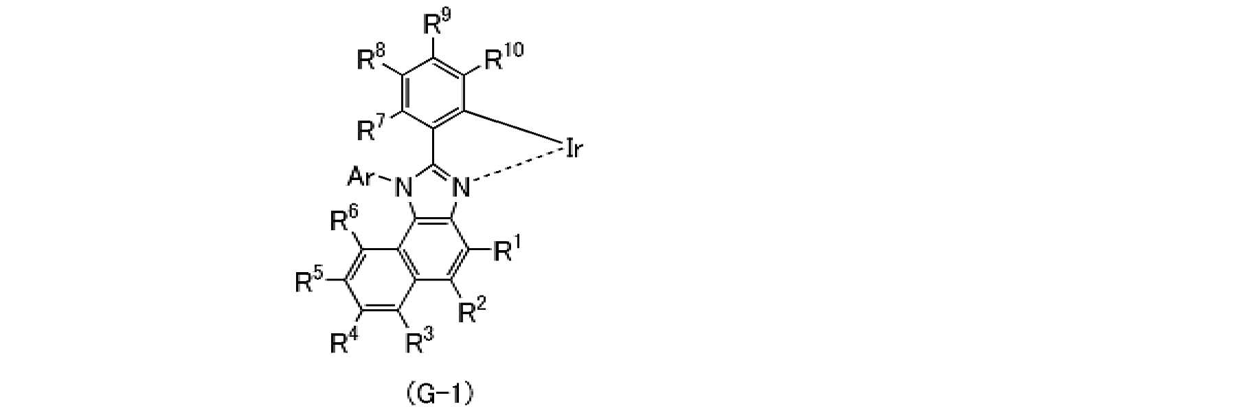
본 발명의 일 형태의 유기 금속 착체는 하기 일반식(G-1)으로 나타내어지는 구조를 가진다. The organometallic complex of one embodiment of the present invention has a structure represented by the following general formula (G-1).
[화학식 18][Formula 18]

일반식(G-1) 중에서, R1 내지 R10은 각각 독립적으로 수소, 탄소수 1 내지 6의 알킬기, 치환 또는 비치환된 탄소수 3 내지 7의 사이클로알킬기, 치환 또는 비치환된 탄소수 6 내지 25의 아릴기, 또는 전자 흡인기를 나타내고, Ar는 치환 또는 비치환된 탄소수 6 내지 25의 아릴기를 나타낸다.In the general formula (G-1), R 1 to R 10 are each independently hydrogen, a
본 발명의 일 형태의 유기 금속 착체는 리간드에 1H-나프토[1,2-d]이미다졸 골격을 가진다. 상기 구성으로 함으로써, 상기 유기 금속 착체를 발광 소자에 적용한 경우, 발광 효율 및/또는 신뢰성이 양호한 발광 소자를 얻을 수 있다. The organometallic complex of one embodiment of the present invention has a 1H-naphtho[1,2-d]imidazole skeleton in its ligand. By setting it as the above configuration, when the organometallic complex is applied to a light-emitting element, a light-emitting element having good luminous efficiency and/or reliability can be obtained.
본 발명의 일 형태의 유기 금속 착체가 가지는 리간드는, 벤즈이미다졸 골격이 가지는 벤젠 고리에 벤젠 고리가 더 축합된 구조를 가진다. 상기 구조로 함으로써, 분자의 안정성이 향상되고, 신뢰성이 양호한 발광 소자를 얻을 수 있다. 또한, 발광 양자 수율이 양호한 유기 금속 착체를 얻을 수 있다. The ligand of the organometallic complex of one embodiment of the present invention has a structure in which a benzene ring is further condensed with a benzene ring of a benzimidazole skeleton. By setting it as the above structure, molecular stability is improved, and a light-emitting device having good reliability can be obtained. In addition, it is possible to obtain an organometallic complex having a good light emission quantum yield.
또한, 1H-나프토[1,2-d]이미다졸 골격의 1위치에 치환 또는 비치환된 탄소수 6 내지 25의 아릴기가 결합됨으로써, 1위치에 수소나 알킬기가 결합된 경우와 비교하여 분자의 안정성 및 승화성이 향상된다. 그러므로, 신뢰성이 양호한 발광 소자를 얻을 수 있다. 또한, 진공 증착법을 사용하여 유기 EL 소자를 제작하는 경우, 본 발명의 일 형태의 유기 화합물을 적합하게 사용할 수 있다. In addition, since a substituted or unsubstituted aryl group having 6 to 25 carbon atoms is bonded to the 1 position of the 1H-naphtho[1,2-d]imidazole skeleton, the molecular weight is compared with the case where a hydrogen or an alkyl group is bonded to the 1 position. Stability and sublimation are improved. Therefore, a light-emitting element having good reliability can be obtained. In addition, in the case of fabricating an organic EL device using a vacuum evaporation method, the organic compound of one embodiment of the present invention can be suitably used.
<이미다졸 골격과 나프탈렌 골격의 축합 위치><Condensation position of imidazole skeleton and naphthalene skeleton>
또한, 본 발명의 일 형태의 유기 금속 착체가 가지는 1H-나프토[1,2-d]이미다졸 골격은 이미다졸 골격에 나프탈렌 골격이 축합된 구조로 간주할 수 있다. 여기서, 나프탈렌 골격이 이미다졸 골격의 a위치에서 축합된 구조를 가지는 경우, 하기 일반식(I-1)으로 나타내어지는 구조를 가지는 Ir 착체를 일례로서 생각할 수 있다. In addition, the 1H-naphtho[1,2-d]imidazole skeleton of one embodiment of the organometallic complex of the present invention can be regarded as a structure in which a naphthalene skeleton is condensed with an imidazole skeleton. Here, when the naphthalene skeleton has a structure condensed at the a-position of the imidazole skeleton, an Ir complex having a structure represented by the following general formula (I-1) can be considered as an example.
[화학식 19][Formula 19]

일반식(I-1) 중에서, R1 내지 R7은 각각 독립적으로 수소, 탄소수 1 내지 6의 알킬기, 치환 또는 비치환된 탄소수 3 내지 7의 사이클로알킬기, 치환 또는 비치환된 탄소수 6 내지 25의 아릴기를 나타낸다.In General Formula (I-1), R 1 to R 7 are each independently hydrogen, a
일반식(I-1)으로 나타내어지는 구조는, Ir에 결합되는 이미다졸 골격과 Ir에 결합되는 벤젠 골격이 서로 축합된 구조를 가진다. 상기 구조는 양자 수율이 높아지지 않는 경향이 있다. 또한, Ir에 결합되는 이미다졸 골격과 Ir에 결합되는 벤젠 골격이 축합되어 있기 때문에, 축합되지 않은 경우와 비교하여 장파장에 발광을 나타내는 것으로 예상된다. 그러므로, 특히 개발이 요구되는 청색이나 녹색의 인광성 재료에는 적합하지 않은 골격인 것으로 예상된다. The structure represented by the general formula (I-1) has a structure in which an imidazole skeleton bonded to Ir and a benzene skeleton bonded to Ir are condensed with each other. The structure does not tend to increase the quantum yield. In addition, since the imidazole skeleton bonded to Ir and the benzene skeleton bonded to Ir are condensed, it is expected to emit light at a longer wavelength compared to the case where condensation is not performed. Therefore, it is expected to be an unsuitable framework for blue or green phosphorescent materials that are required to be developed.
한편, 본 발명의 일 형태의 유기 금속 착체가 가지는 1H-나프토[1,2-d]이미다졸 골격은 이미다졸 골격의 d위치에 나프탈렌 골격이 축합된 구조를 가진다. 여기서, 이미다졸 골격의 d위치에 나프탈렌 골격이 축합되는 경우, 축합 위치의 차이에 의하여 1H-나프토[1,2-d]이미다졸 골격과 1H-나프토[2,1-d]이미다졸 골격을 생각할 수 있다. 이들 축합 탄소의 차이로 인한 양자 수율에 대한 영향을 분자 궤도 계산에 의하여 고찰하였다. Meanwhile, the 1H-naphtho[1,2-d]imidazole skeleton of one embodiment of the organometallic complex of the present invention has a structure in which a naphthalene skeleton is condensed at the d-position of the imidazole skeleton. Here, when the naphthalene skeleton is condensed at the d-position of the imidazole skeleton, the 1H-naphtho[1,2-d]imidazole skeleton and the 1H-naphtho[2,1-d]imidazole are due to the difference in the condensation position. I can think of a skeleton. The influence on the quantum yield due to the difference between these condensed carbons was investigated by molecular orbital calculation.
<알짜 전하의 계산 예><Example of calculation of net charge>
본 계산 예에서는, 본 발명의 일 형태인 1H-나프토[1,2-d]이미다졸 골격을 가지는 유기 금속 착체를 모델로 한 Compound-A와, 비교로서 1H-나프토[2,1-d]이미다졸 골격을 가지는 유기 금속 착체를 모델로 한 Compound-B의 최저 삼중항 들뜬 상태(T1 상태)의 계산 예를 구체적으로 예시한다. Compound-A 및 Compound-B의 구조를 이하에 나타내었다. Compound-A는 구조식 내에 나타내는 a의 벤젠 고리가 Ir와 결합되어 있는 N(질소)으로부터 보았을 때 Ir와 반대 측에 축합되어 있다. 한편, Compound-B에서는, 구조식 내에 나타내는 b의 벤젠 고리가 Ir와 결합되어 있는 N(질소)으로부터 보았을 때 Ir와 같은 측에 축합되어 있다. 1H-나프토[2,1-d]이미다졸 골격을 Ir 착체의 리간드로서 사용한 경우, Compound-B와 같은 방향에 벤젠 고리가 축합된 구조를 가진다.In this calculation example, Compound-A modeled on an organometallic complex having a 1H-naphtho[1,2-d]imidazole skeleton, which is one embodiment of the present invention, and 1H-naphtho[2,1- d] An example of calculation of the lowest triplet excited state (T 1 state) of Compound-B modeled on an organometallic complex having an imidazole skeleton will be specifically illustrated. The structures of Compound-A and Compound-B are shown below. Compound-A is condensed on the opposite side of Ir when viewed from N (nitrogen) in which the benzene ring of a represented in the structural formula is bonded to Ir. On the other hand, in Compound-B, the benzene ring of b shown in the structural formula is condensed on the same side as Ir when viewed from N (nitrogen) bonded to Ir. When the 1H-naphtho[2,1-d]imidazole skeleton is used as a ligand for the Ir complex, it has a structure in which a benzene ring is condensed in the same direction as Compound-B.
[화학식 20][Formula 20]

분자 궤도 계산에는, Gaussian09 프로그램을 사용하였다. 범함수에는 B3PW91을 사용하고, 구조 최적화 및 진동 계산을 수행하였다. 기저 함수는, Ir에 LANL2DZ를, 이 외의 원소에는 6-311G를 사용하였다. The Gaussian09 program was used for molecular orbital calculation. B3PW91 was used as the functional function, and structure optimization and vibration calculation were performed. As the basis function, LANL2DZ was used for Ir and 6-311G was used for other elements.
계산으로 구한 최적화 구조에서의 Ir 위의 알짜 전하는 Compound-A에서 0.30으로, Compound-B에서는 0.20으로 산출되었다. The net charge on Ir in the calculated optimized structure was calculated as 0.30 in Compound-A and 0.20 in Compound-B.
Compound-A는 Compound-B보다 Ir의 알짜 전하가 우위하게 높아지는 결과를 얻을 수 있었다. Metal-Ligand Charge Transfer(MLCT)는 Ir의 5d 궤도와 리간드의 π*가 기여하는 전이이다. MLCT성이 높은 요인 중 하나로서 들뜬 상태에서 Ir의 알짜 전하가 높은 것을 들 수 있다. 따라서, 본 발명의 일 형태인 유기 금속 착체를 모델로 한 Compound-A는 Compound-B보다 들뜬 상태에서의 MLCT성이 더 높다는 것을 알 수 있었다. MLCT성과 인광성 재료의 양자 수율에는 상관이 있다는 것이 알려져 있으며, MLCT성이 높으면 발광 양자 수율이 높은 것으로 예상된다. 따라서, 본 발명의 일 형태의 유기 화합물은 높은 발광 양자 수율을 가진다는 것을 알 수 있었다.Compound-A was able to obtain a result that the net charge of Ir was higher than that of Compound-B. Metal-Ligand Charge Transfer (MLCT) is a transition contributed by the 5d orbital of Ir and π * of the ligand. One of the factors of high MLCT property is that the net charge of Ir is high in the excited state. Accordingly, it was found that Compound-A, modeled on an organometallic complex, which is one embodiment of the present invention, has higher MLCT properties in an excited state than Compound-B. It is known that there is a correlation between the MLCT property and the quantum yield of the phosphorescent material, and it is expected that the emission quantum yield is high when the MLCT property is high. Accordingly, it was found that the organic compound of one embodiment of the present invention has a high light emission quantum yield.
Compound-B는 구조식 중에서 b로 나타낸 벤젠 고리가 Ir와 입체 장애를 일으키는 방향으로 존재한다. 그러므로, Compound-B에서는 Ir와 이미다졸 골격이 가지는 N(질소)과의 결합 거리가 길어지는 것으로 예상된다. 그러므로 상술한 바와 같이 Ir 위의 알짜 전하가 Compound-B에서는 작아진 것으로 생각된다. 1H-나프토[2,1-d]이미다졸 골격을 가지는 Ir 착체도 구조식 중의 b로 나타낸 벤젠 고리를 가지기 때문에, Compound-B와 마찬가지로 알짜 전하가 작은 것으로 생각된다. 한편, Compound-A가 가지는 구조식 중에서 a로 나타낸 벤젠 고리는 Ir와 입체 장애를 일으키지 않았다. 그러므로, Compound-B보다 알짜 전하가 크다는 결과가 얻어진 것으로 생각된다. Compound-B exists in a direction in which the benzene ring represented by b in the structural formula causes steric hindrance with Ir. Therefore, in Compound-B, the bonding distance between Ir and N (nitrogen) of the imidazole skeleton is expected to increase. Therefore, as described above, the net charge on Ir is considered to be small in Compound-B. Since the Ir complex having a 1H-naphtho[2,1-d]imidazole skeleton also has a benzene ring represented by b in the structural formula, it is considered to have a small net charge like Compound-B. On the other hand, in the structural formula of Compound-A, the benzene ring represented by a did not cause steric hindrance with Ir. Therefore, it is thought that the result was obtained that the net charge was larger than that of Compound-B.
이상으로부터, 이미다졸 골격에 나프탈렌 골격이 축합된 구조를 가지는 유기 금속 착체를 고려한 경우, 1H-나프토[1,2-d]이미다졸 골격으로 함으로써 발광 양자 수율이 양호한 유기 금속 착체를 얻을 수 있다. From the above, when an organometallic complex having a structure in which a naphthalene skeleton is condensed in an imidazole skeleton is considered, an organometallic complex having a good light emission quantum yield can be obtained by using a 1H-naphtho[1,2-d]imidazole skeleton. .
상기 탄소수 6 내지 25의 아릴기는 치환 또는 비치환된 페닐기인 것이 바람직하다. 상기 구성으로 함으로써, 저렴하고 용이하게 본 발명의 일 형태의 유기 금속 착체를 합성할 수 있다. 따라서, 일반식(G-1)은 하기 일반식(G-2)으로 나타내어지는 구조인 것이 바람직하다. The aryl group having 6 to 25 carbon atoms is preferably a substituted or unsubstituted phenyl group. By setting it as the above structure, the organometallic complex of one embodiment of the present invention can be synthesized inexpensively and easily. Therefore, it is preferable that general formula (G-1) is a structure represented by the following general formula (G-2).
[화학식 21][Formula 21]

일반식(G-2) 중에서, R1 내지 R15는 각각 독립적으로 수소, 탄소수 1 내지 6의 알킬기, 치환 또는 비치환된 탄소수 3 내지 7의 사이클로알킬기, 치환 또는 비치환된 탄소수 6 내지 25의 아릴기, 또는 전자 흡인기를 나타낸다.In the general formula (G-2), R 1 to R 15 are each independently hydrogen, a
또한, 본 발명의 일 형태의 유기 금속 착체는 하기 일반식(G-3)으로 나타내어지는 구조를 가진다. In addition, the organometallic complex of one embodiment of the present invention has a structure represented by the following general formula (G-3).
[화학식 22][Formula 22]

일반식(G-3) 중에서, R11, R13, 및 R15는 각각 독립적으로 수소, 탄소수 1 내지 6의 알킬기, 치환 또는 비치환된 탄소수 3 내지 7의 사이클로알킬기, 치환 또는 비치환된 탄소수 6 내지 25의 아릴기, 또는 전자 흡인기를 나타낸다.In the general formula (G-3), R 11 , R 13 , and R 15 are each independently hydrogen, an alkyl group having 1 to 6 carbon atoms, a substituted or unsubstituted cycloalkyl group having 3 to 7 carbon atoms, and a substituted or unsubstituted carbon number. 6 to 25 aryl groups or electron withdrawing groups are shown.
일반식(G-2) 및 (G-3)에서, R11 및 R15 중 적어도 한쪽이 탄소수 1 내지 6의 알킬기인 것이 바람직하다. 상기 구성으로 함으로써, 승화성이 좋은 재료로 할 수 있기 때문에, 진공 증착법에 의한 발광 소자 제작 시에, 재료 사용 효율을 높일 수 있다. 또한, R11 및 R15가 결합되는 페닐기는, R11 및 R15 중 적어도 한쪽이 탄소수 1 내지 6의 알킬기인 경우, 상기 알킬기의 입체 장애에 의하여 상기 페닐기와 1H-나프토[1,2-d]이미다졸 골격이 이루는 이면각이 커진다. 그러므로, 상기 페닐기와 1H-나프토[1,2-d]이미다졸 골격 간의 공액이 확대되기 어려워지므로, 발광 파장을 단파장화시킬 수 있다. 또한, 상기 알킬기는 탄소수 3 내지 7의 분지쇄 알킬기인 것이 더 바람직하다. 분지쇄 알킬기임으로써, 상술한 효과를 더 얻기 쉬워진다. 분지쇄 알킬기로서는, 아이소프로필기, 아이소뷰틸기, 삼차 뷰틸기 등을 들 수 있다.In general formulas (G-2) and (G-3) , it is preferable that at least one of R 11 and R 15 is an alkyl group having 1 to 6 carbon atoms. By setting it as the above structure, since it can be made into a material with good sublimation property, when manufacturing a light emitting element by a vacuum evaporation method, material use efficiency can be improved. In addition, the phenyl group to which R 11 and R 15 are bonded is, when at least one of R 11 and R 15 is an alkyl group having 1 to 6 carbon atoms, the phenyl group and 1H-naphtho[1,2- d] The dihedral angle formed by the imidazole skeleton increases. Therefore, since the conjugation between the phenyl group and the 1H-naphtho[1,2-d]imidazole skeleton becomes difficult to expand, the emission wavelength can be shortened. Further, the alkyl group is more preferably a branched chain alkyl group having 3 to 7 carbon atoms. By being a branched chain alkyl group, it becomes easier to obtain the above-described effect. As a branched chain alkyl group, an isopropyl group, an isobutyl group, a tertiary butyl group, etc. are mentioned.
따라서, 본 발명의 일 형태의 유기 금속 착체는 하기 일반식(G-4)으로 나타내어지는 구조를 가진다. Accordingly, the organometallic complex of one embodiment of the present invention has a structure represented by the following general formula (G-4).
[화학식 23][Formula 23]
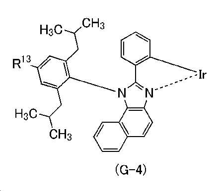
일반식(G-4) 중에서, R13은 수소 또는 전자 흡인기를 나타낸다.In General Formula (G-4), R 13 represents hydrogen or an electron withdrawing group.
일반식(G-4)에서, R13이 수소인 경우, 합성이 용이하게 되기 때문에 바람직하다. 또한, R13이 전자 흡인기인 경우, 유기 금속 착체의 LUMO(Lowest Unoccupied Molecular Orbital, 최저 비점유 분자 궤도라고도 함) 준위 및 HOMO(Highest Occupied Molecular Orbital, 최고 점유 분자 궤도라고도 함) 준위를 낮출 수 있다. 따라서, 유기 금속 착체를 발광 소자에 사용한 경우에 있어서, 정공 주입성을 유지하면서 전자 주입성을 높일 수 있어, 발광 효율을 향상시킬 수 있다. 또한, CT(Charge Transfer)성이 높아지는 것을 기대할 수 있고, 스펙트럼 폭이 넓어지는 것이 전망된다. 그러므로, 연색성이 높은 발광 소자를 제작할 수 있다.In the general formula (G-4), when R 13 is hydrogen, it is preferable because synthesis becomes easy. In addition, when R 13 is an electron withdrawing group, the level of the LUMO (Lowest Unoccupied Molecular Orbital, also called the lowest unoccupied molecular orbital) and the Highest Occupied Molecular Orbital (HOMO) level of the organometallic complex can be lowered. . Therefore, when the organic metal complex is used for a light emitting device, it is possible to improve the electron injection property while maintaining the hole injection property, thereby improving the luminous efficiency. In addition, the CT (Charge Transfer) property can be expected to increase, and the spectrum width is expected to be widened. Therefore, a light-emitting element having high color rendering properties can be manufactured.
또한, 본 발명의 일 형태의 유기 금속 착체는 하기 일반식(G-5)으로 나타내어지는 유기 금속 착체이다. In addition, the organometallic complex of one embodiment of the present invention is an organometallic complex represented by the following general formula (G-5).
[화학식 24][Formula 24]

일반식(G-5) 중에서, R15는 수소, 탄소수 1 내지 6의 알킬기, 치환 또는 비치환된 탄소수 3 내지 7의 사이클로알킬기, 치환 또는 비치환된 탄소수 6 내지 25의 아릴기를 나타낸다.In General Formula (G-5), R 15 represents hydrogen, an alkyl group having 1 to 6 carbon atoms, a substituted or unsubstituted cycloalkyl group having 3 to 7 carbon atoms, and a substituted or unsubstituted aryl group having 6 to 25 carbon atoms.
상술한 바와 같이, 1H-나프토[1,2-d]이미다졸의 1위치에 결합하는 페닐기의 4위치에 전자 흡인기인 사이아노기를 도입함으로써, 발광 효율이 양호한 발광 소자를 제작할 수 있다. 또한, 연색성이 높은 발광 소자를 제작할 수 있다. As described above, by introducing a cyano group, which is an electron withdrawing group, at the 4 position of the phenyl group bonded to the 1 position of 1H-naphtho[1,2-d]imidazole, a light emitting device having good luminous efficiency can be manufactured. In addition, a light-emitting device having high color rendering properties can be manufactured.
또한, 본 발명의 일 형태의 유기 금속 착체는 하기 일반식(G-6)으로 나타내어지는 유기 금속 착체이다. In addition, the organometallic complex of one embodiment of the present invention is an organometallic complex represented by the following general formula (G-6).
[화학식 25][Formula 25]

일반식(G-6) 중에서, R1 내지 R10은 각각 독립적으로 수소, 탄소수 1 내지 6의 알킬기, 치환 또는 비치환된 탄소수 3 내지 7의 사이클로알킬기, 치환 또는 비치환된 탄소수 6 내지 25의 아릴기, 또는 전자 흡인기를 나타내고, Ar는 치환 또는 비치환된 탄소수 6 내지 25의 아릴기를 나타낸다.In the general formula (G-6), R 1 to R 10 are each independently hydrogen, a
일반식(G-6)으로 나타내어지는 유기 금속 착체는 일반식(G-1)으로 나타내어지는 유기 금속 착체 중, 유기 금속 착체가 가지는 3종류의 리간드가 모두 동일한 리간드인 트리스체를 나타낸다. 트리스체의 유기 금속 착체는 발광 효율, 신뢰성이 양호하기 때문에 바람직하다. The organometallic complex represented by the general formula (G-6) represents a tris form in which all three kinds of ligands of the organometallic complex are the same among the organometallic complexes represented by the general formula (G-1). Tris body organometallic complexes are preferable because of good luminous efficiency and reliability.
또한, 본 발명의 일 형태의 유기 금속 착체는 하기 일반식(G-7)으로 나타내어지는 유기 금속 착체이다. In addition, the organometallic complex of one embodiment of the present invention is an organometallic complex represented by the following general formula (G-7).
[화학식 26][Formula 26]

일반식(G-7) 중에서, R1 내지 R15는 각각 독립적으로 수소, 탄소수 1 내지 6의 알킬기, 치환 또는 비치환된 탄소수 3 내지 7의 사이클로알킬기, 치환 또는 비치환된 탄소수 6 내지 25의 아릴기, 또는 전자 흡인기를 나타낸다.In the general formula (G-7), R 1 to R 15 are each independently hydrogen, a
일반식(G-7)으로 나타내어지는 유기 금속 착체는 일반식(G-2)으로 나타내어지는 유기 금속 착체 중, 유기 금속 착체가 가지는 3종류의 리간드가 모두 동일한 리간드인 트리스체를 나타낸다. 트리스체의 유기 금속 착체는 발광 효율, 신뢰성이 양호하기 때문에 바람직하다. The organometallic complex represented by the general formula (G-7) represents a tris form in which all three kinds of ligands of the organometallic complex are the same among the organometallic complexes represented by the general formula (G-2). Tris body organometallic complexes are preferable because of good luminous efficiency and reliability.
또한, 본 발명의 일 형태의 유기 금속 착체는 하기 일반식(G-8)으로 나타내어지는 유기 금속 착체이다. In addition, the organometallic complex of one embodiment of the present invention is an organometallic complex represented by the following general formula (G-8).
[화학식 27][Formula 27]

일반식(G-8) 중에서, R11, R13, 및 R15는 각각 독립적으로 수소, 탄소수 1 내지 6의 알킬기, 치환 또는 비치환된 탄소수 3 내지 7의 사이클로알킬기, 치환 또는 비치환된 탄소수 6 내지 25의 아릴기, 또는 전자 흡인기를 나타낸다.In the general formula (G-8), R 11 , R 13 , and R 15 are each independently hydrogen, an alkyl group having 1 to 6 carbon atoms, a substituted or unsubstituted cycloalkyl group having 3 to 7 carbon atoms, and a substituted or unsubstituted carbon number. 6 to 25 aryl groups or electron withdrawing groups are shown.
일반식(G-8)으로 나타내어지는 유기 금속 착체는 일반식(G-3)으로 나타내어지는 유기 금속 착체 중, 유기 금속 착체가 가지는 3종류의 리간드가 모두 동일한 리간드인 트리스체를 나타낸다. 트리스체의 유기 금속 착체는 발광 효율, 신뢰성이 양호하기 때문에 바람직하다. The organometallic complex represented by the general formula (G-8) represents a tris form in which all three kinds of ligands of the organometallic complex are the same among the organometallic complexes represented by the general formula (G-3). Tris body organometallic complexes are preferable because of good luminous efficiency and reliability.
또한, 본 발명의 일 형태의 유기 금속 착체는 하기 일반식(G-9)으로 나타내어지는 유기 금속 착체이다. In addition, the organometallic complex of one embodiment of the present invention is an organometallic complex represented by the following general formula (G-9).
[화학식 28][Formula 28]

일반식(G-9) 중에서, R13은 수소 또는 전자 흡인기를 나타낸다.In General Formula (G-9), R 13 represents hydrogen or an electron withdrawing group.
일반식(G-9)으로 나타내어지는 유기 금속 착체는 일반식(G-4)으로 나타내어지는 유기 금속 착체 중, 유기 금속 착체가 가지는 3종류의 리간드가 모두 동일한 리간드인 트리스체를 나타낸다. 트리스체의 유기 금속 착체는 발광 효율, 신뢰성이 양호하기 때문에 바람직하다. The organometallic complex represented by the general formula (G-9) represents a tris form in which all three kinds of ligands of the organometallic complex are the same among the organometallic complexes represented by the general formula (G-4). Tris body organometallic complexes are preferable because of good luminous efficiency and reliability.
또한, 본 발명의 일 형태의 유기 금속 착체는 하기 일반식(G-10)으로 나타내어지는 유기 금속 착체이다. In addition, the organometallic complex of one embodiment of the present invention is an organometallic complex represented by the following general formula (G-10).
[화학식 29][Formula 29]

일반식(G-10) 중에서, R15는 수소, 탄소수 1 내지 6의 알킬기, 치환 또는 비치환된 탄소수 3 내지 7의 사이클로알킬기, 치환 또는 비치환된 탄소수 6 내지 25의 아릴기를 나타낸다.In General Formula (G-10), R 15 represents hydrogen, an alkyl group having 1 to 6 carbon atoms, a substituted or unsubstituted cycloalkyl group having 3 to 7 carbon atoms, and a substituted or unsubstituted aryl group having 6 to 25 carbon atoms.
일반식(G-10)으로 나타내어지는 유기 금속 착체는 일반식(G-5)으로 나타내어지는 유기 금속 착체 중, 유기 금속 착체가 가지는 3종류의 리간드가 모두 동일한 리간드인 트리스체를 나타낸다. 트리스체의 유기 금속 착체는 발광 효율, 신뢰성이 양호하기 때문에 바람직하다. The organometallic complex represented by the general formula (G-10) represents a tris form in which all three kinds of ligands of the organometallic complex are the same among the organometallic complexes represented by the general formula (G-5). Tris body organometallic complexes are preferable because of good luminous efficiency and reliability.
또한, 본 발명의 일 형태의 유기 금속 착체는 하기 일반식(G-11)으로 나타내어지는 유기 금속 착체이다. In addition, the organometallic complex of one embodiment of the present invention is an organometallic complex represented by the following general formula (G-11).
[화학식 30][Formula 30]

일반식(G-11) 중에서, R1 내지 R10은 각각 독립적으로 수소, 탄소수 1 내지 6의 알킬기, 치환 또는 비치환된 탄소수 3 내지 7의 사이클로알킬기, 치환 또는 비치환된 탄소수 6 내지 25의 아릴기, 또는 전자 흡인기를 나타내고, Ar는 치환 또는 비치환된 탄소수 6 내지 25의 아릴기를 나타내고, L은 일가음이온성의 리간드를 나타내고, n은 1 또는 2를 나타낸다.In the general formula (G-11), R 1 to R 10 are each independently hydrogen, a
일반식(G-11)으로 나타내어지는 유기 금속 착체는 일반식(G-1)으로 나타내어지는 유기 금속 착체 중, 2종류 이상의 리간드를 가지는 유기 금속 착체인 헤테로체를 나타낸다. 헤테로체의 유기 금속 착체는 리간드의 조합을 선택함으로써, 발광색이나 승화성을 조정할 수 있기 때문에 바람직하다. The organometallic complex represented by the general formula (G-11) represents a heteroform which is an organometallic complex having two or more types of ligands among the organometallic complexes represented by the general formula (G-1). The organometallic complex of a hetero body is preferable because luminescence color and sublimation property can be adjusted by selecting a combination of ligands.
또한, 본 발명의 일 형태의 유기 금속 착체는 하기 일반식(G-12)으로 나타내어지는 유기 금속 착체이다. In addition, the organometallic complex of one embodiment of the present invention is an organometallic complex represented by the following general formula (G-12).
[화학식 31][Chemical Formula 31]

일반식(G-12) 중에서, R1 내지 R15는 각각 독립적으로 수소, 탄소수 1 내지 6의 알킬기, 치환 또는 비치환된 탄소수 3 내지 7의 사이클로알킬기, 치환 또는 비치환된 탄소수 6 내지 25의 아릴기, 또는 전자 흡인기를 나타내고, L은 일가음이온성의 리간드를 나타내고, n은 1 또는 2를 나타낸다.In the general formula (G-12), R 1 to R 15 are each independently hydrogen, a
일반식(G-12)으로 나타내어지는 유기 금속 착체는 일반식(G-2)으로 나타내어지는 유기 금속 착체 중, 2종류 이상의 리간드를 가지는 금속 착체인 헤테로체를 나타낸다. 헤테로체의 유기 금속 착체는 리간드의 조합을 선택함으로써, 발광색이나 승화성을 조정할 수 있기 때문에 바람직하다. The organometallic complex represented by the general formula (G-12) represents a heteroform which is a metal complex having two or more kinds of ligands among the organometallic complexes represented by the general formula (G-2). The organometallic complex of a hetero body is preferable because luminescence color and sublimation property can be adjusted by selecting a combination of ligands.
또한, 본 발명의 일 형태의 유기 금속 착체는 하기 일반식(G-13)으로 나타내어지는 유기 금속 착체이다. In addition, the organometallic complex of one embodiment of the present invention is an organometallic complex represented by the following general formula (G-13).
[화학식 32][Formula 32]

일반식(G-13) 중에서, R11, R13, 및 R15는 각각 독립적으로 수소, 탄소수 1 내지 6의 알킬기, 치환 또는 비치환된 탄소수 3 내지 7의 사이클로알킬기, 치환 또는 비치환된 탄소수 6 내지 25의 아릴기, 또는 전자 흡인기를 나타내고, L은 일가음이온성의 리간드를 나타내고, n은 1 또는 2를 나타낸다.In the general formula (G-13), R 11 , R 13 , and R 15 are each independently hydrogen, an alkyl group having 1 to 6 carbon atoms, a substituted or unsubstituted cycloalkyl group having 3 to 7 carbon atoms, and a substituted or unsubstituted carbon number. 6 to 25 aryl groups or electron withdrawing groups are represented, L represents a monoanionic ligand, and n represents 1 or 2.
일반식(G-13)으로 나타내어지는 유기 금속 착체는 일반식(G-3)으로 나타내어지는 유기 금속 착체 중, 2종류 이상의 리간드를 가지는 금속 착체인 헤테로체를 나타낸다. 헤테로체의 유기 금속 착체는 리간드의 조합을 선택함으로써, 발광색이나 승화성을 조정할 수 있기 때문에 바람직하다. The organometallic complex represented by the general formula (G-13) represents a heterobody which is a metal complex having two or more kinds of ligands among the organometallic complexes represented by the general formula (G-3). The organometallic complex of a hetero body is preferable because luminescence color and sublimation property can be adjusted by selecting a combination of ligands.
또한, 본 발명의 일 형태의 유기 금속 착체는 하기 일반식(G-14)으로 나타내어지는 유기 금속 착체이다. In addition, the organometallic complex of one embodiment of the present invention is an organometallic complex represented by the following general formula (G-14).
[화학식 33][Formula 33]

일반식(G-14) 중에서, R13은 수소 또는 전자 흡인기를 나타내고, L은 일가음이온성의 리간드를 나타내고, n은 1 또는 2를 나타낸다.In General Formula (G-14), R 13 represents hydrogen or an electron withdrawing group, L represents a monoanionic ligand, and n represents 1 or 2.
일반식(G-14)으로 나타내어지는 유기 금속 착체는 일반식(G-4)으로 나타내어지는 유기 금속 착체 중, 2종류 이상의 리간드를 가지는 금속 착체인 헤테로체를 나타낸다. 헤테로체의 유기 금속 착체는 리간드의 조합을 선택함으로써, 발광색이나 승화성을 조정할 수 있기 때문에 바람직하다. The organometallic complex represented by the general formula (G-14) represents a heteroform which is a metal complex having two or more kinds of ligands among the organometallic complexes represented by the general formula (G-4). The organometallic complex of a hetero body is preferable because luminescence color and sublimation property can be adjusted by selecting a combination of ligands.
또한, 본 발명의 일 형태의 유기 금속 착체는 하기 일반식(G-15)으로 나타내어지는 유기 금속 착체이다. In addition, the organometallic complex of one embodiment of the present invention is an organometallic complex represented by the following general formula (G-15).
[화학식 34][Formula 34]

일반식(G-15) 중에서, R15는 수소, 탄소수 1 내지 6의 알킬기, 치환 또는 비치환된 탄소수 3 내지 7의 사이클로알킬기, 치환 또는 비치환된 탄소수 6 내지 25의 아릴기를 나타내고, L은 일가음이온성의 리간드를 나타내고, n은 1 또는 2를 나타낸다.In the general formula (G-15), R 15 represents hydrogen, an alkyl group having 1 to 6 carbon atoms, a substituted or unsubstituted cycloalkyl group having 3 to 7 carbon atoms, a substituted or unsubstituted aryl group having 6 to 25 carbon atoms, and L is Represents a monoanionic ligand, and n represents 1 or 2.
일반식(G-15)으로 나타내어지는 유기 금속 착체는 일반식(G-5)으로 나타내어지는 유기 금속 착체 중, 2종류 이상의 리간드를 가지는 금속 착체인 헤테로체를 나타낸다. 헤테로체의 유기 금속 착체는 리간드의 조합을 선택함으로써, 발광색이나 승화성을 조정할 수 있기 때문에 바람직하다. The organometallic complex represented by the general formula (G-15) represents a heteroform which is a metal complex having two or more kinds of ligands among the organometallic complexes represented by the general formula (G-5). The organometallic complex of a hetero body is preferable because luminescence color and sublimation property can be adjusted by selecting a combination of ligands.
또한, 일반식(G-11) 내지 (G-15) 중에서, L로 나타내어지는 일가음이온성의 리간드는 β-다이케톤 구조를 가지는 일가음이온성의 2좌 킬레이트 리간드, 카복실기를 가지는 일가음이온성의 2좌 킬레이트 리간드, 페놀성 수산기를 가지는 일가음이온성의 2좌 킬레이트 리간드, 또는 2개의 배위 원소가 모두 질소인 일가음이온성의 2좌 킬레이트 리간드, 또는 사이클로 메탈화에 의하여 이리듐과 금속-탄소 결합을 형성하는 2좌 리간드인 것이 바람직하다. 구체적으로는, 하기 일반식(L1) 내지 (L9) 중 어느 것인 것이 바람직하다. In addition, in the general formulas (G-11) to (G-15), the monoanionic ligand represented by L is a monoanionic bidentate chelate ligand having a β-diketone structure, a monoanionic bidentate chelate having a carboxyl group. A ligand, a monoanionic bidentate chelate ligand having a phenolic hydroxyl group, or a monoanionic bidentate chelate ligand in which both coordination elements are nitrogen, or a bidentate ligand that forms a metal-carbon bond with iridium by cyclometallization. It is preferable to be. Specifically, any one of the following general formulas (L1) to (L9) is preferable.
[화학식 35][Formula 35]

일반식(L1) 내지 (L9) 중, R21 내지 R86은 각각 독립적으로 수소, 치환 또는 비치환된 탄소수 1 내지 6의 알킬기, 할로제노기, 바이닐기, 사이아노기, 치환 또는 비치환된 탄소수 1 내지 6의 할로알킬기, 치환 또는 비치환된 탄소수 1 내지 6의 알콕시기, 또는 치환 또는 비치환된 탄소수 1 내지 6의 알킬싸이오기, 치환 또는 비치환된 탄소수 6 내지 13의 아릴기를 나타낸다. 또한, A1 내지 A13은 각각 독립적으로 질소, 또는 수소와 결합하는 sp2 혼성 탄소, 또는 치환기를 가지는 sp2 혼성 탄소를 나타내고, 상기 치환기는 탄소수 1 내지 6의 알킬기, 할로제노기, 탄소수 1 내지 6의 할로알킬기, 및 페닐기 중 어느 것을 나타낸다.In the general formulas (L1) to (L9), R 21 to R 86 are each independently hydrogen, a substituted or unsubstituted alkyl group having 1 to 6 carbon atoms, a halogeno group, a vinyl group, a cyano group, a substituted or unsubstituted A haloalkyl group having 1 to 6 carbon atoms, a substituted or unsubstituted alkoxy group having 1 to 6 carbon atoms, or a substituted or unsubstituted alkylthio group having 1 to 6 carbon atoms, or a substituted or unsubstituted aryl group having 6 to 13 carbon atoms. In addition, A 1 to A 13 each independently represent nitrogen or sp 2 hybrid carbon bonded to hydrogen, or sp 2 hybrid carbon having a substituent, and the substituent is an alkyl group having 1 to 6 carbon atoms, a halogeno group, and 1 carbon number. Any of the haloalkyl groups of to 6 and the phenyl group is shown.
여기서, 헤테로체의 유기 금속 착체는 복수 종류의 리간드를 가지지만, 유기 금속 착체의 HOMO 및 LUMO는 동일 종류의 리간드에 분포되는 것이 바람직하다. 상기 구성의 경우, 발광 효율이 특히 양호한 유기 금속 착체로 할 수 있다. 그러므로, 일반식(G-11) 내지 (G-15) 중에서, L은 (L8) 또는 (L9)인 것이 특히 바람직하다. 본 발명의 일 형태의 유기 금속 착체는, 5원 고리인 이미다졸 골격을 가진다. 그러므로, L도 5원 고리 골격을 가지는 구조인 것이 바람직하다. 상기 구성으로 함으로써, 유기 금속 착체가 가지는 HOMO 및 LUMO가 동일한 리간드에 분포되기 쉬워진다. Here, the organometallic complex of the heterostructure has a plurality of types of ligands, but the HOMO and LUMO of the organometallic complex are preferably distributed in the same type of ligand. In the case of the above configuration, an organometallic complex having particularly good luminous efficiency can be obtained. Therefore, in General Formulas (G-11) to (G-15), it is particularly preferable that L is (L8) or (L9). The organometallic complex of one embodiment of the present invention has an imidazole skeleton which is a 5-membered ring. Therefore, it is preferable that L is also a structure having a 5-membered ring skeleton. By setting it as the above structure, the HOMO and LUMO of the organometallic complex are likely to be distributed in the same ligand.
<치환기의 예><Example of substituent>
일반식(G-1) 내지 (G-15)에서, R1 내지 R15는, 예를 들어 수소, 탄소수 1 내지 6의 알킬기, 치환 또는 비치환된 탄소수 3 내지 7의 사이클로알킬기, 또는 치환 또는 비치환된 탄소수 6 내지 25의 아릴기, 또는 전자 흡인기를 나타낸다. 상기 알킬기로서는, 예를 들어 메틸기, 에틸기, 프로필기, 아이소프로필기, 뷰틸기, 아이소뷰틸기, tert-뷰틸기, n-헥실기 등을 들 수 있고, 상기 사이클로알킬기로서는, 예를 들어 사이클로프로필기, 사이클로뷰틸기, 사이클로펜틸기, 사이클로헥실기 등을 들 수 있고, 상기 아릴기로서는, 페닐기, 나프틸기, 바이페닐기, 플루오렌일기, 스파이로플루오렌일기 등을 들 수 있고, 상기 전자 흡인기로서는, 할로제노기, 사이아노기, 나이트로기, 카보닐기, 할로알킬기, 할로알킬기로서는 특히 트라이플루오로메틸기 등을 구체적인 예로서 들 수 있다. 더 구체적으로는, 예를 들어 하기 구조식(R-1) 내지 (R-43)으로 나타내어지는 기를 들 수 있다. 특히, 할로제노기, 사이아노기, 트라이플루오로메틸기는 전자 흡인성이 크고, 안정성이 높기 때문에 바람직하다. 또한, R1 내지 R4 및 R5 내지 R13으로 나타내어지는 기는 이들에 한정되지 않는다.In the general formulas (G-1) to (G-15), R 1 to R 15 are, for example, hydrogen, an alkyl group having 1 to 6 carbon atoms, a substituted or unsubstituted cycloalkyl group having 3 to 7 carbon atoms, or a substituted or It represents an unsubstituted C6-C25 aryl group or an electron withdrawing group. Examples of the alkyl group include methyl group, ethyl group, propyl group, isopropyl group, butyl group, isobutyl group, tert-butyl group, n-hexyl group, and the like, and examples of the cycloalkyl group include cyclopropyl Group, a cyclobutyl group, a cyclopentyl group, a cyclohexyl group, and the like, and examples of the aryl group include a phenyl group, a naphthyl group, a biphenyl group, a fluorenyl group, a spirofluorenyl group, and the like, and the electron withdrawing group Specific examples include a halogeno group, a cyano group, a nitro group, a carbonyl group, a haloalkyl group, and a haloalkyl group, particularly a trifluoromethyl group. More specifically, groups represented by the following structural formulas (R-1) to (R-43) are exemplified. Particularly, a halogeno group, a cyano group, and a trifluoromethyl group are preferable because of their high electron attraction properties and high stability. In addition, the group represented by R 1 to R 4 and R 5 to R 13 is not limited to these.
[화학식 36][Chemical Formula 36]

이때, R1 내지 R10이 수소인 경우, 본 발명의 일 형태의 유기 금속 착체를 간편하고 저렴하게 합성할 수 있다. 전기 화학적으로 안정적이고 신뢰성이 양호하게 되어 바람직하다. 또한, 수소 이외의 치환기이면, 본 발명의 일 형태의 유기 금속 착체의 내열성을 향상시킬 수 있다. (R-2) 내지 (R-15)와 같이, 알킬기나 사이클로알킬기이면 유기 용제에 대한 용해성이 양호하기 때문에, 본 발명의 일 형태의 유기 금속 착체의 정제를 간편하게 수행할 수 있다. (R-16), (R-22) 내지 (R-28), (R-31) 및 (R-32)와 같이, 알킬기나 사이클로알킬기를 가지지 않는 아릴기는 전기 화학적으로 안정적이고 신뢰성이 양호하다.At this time, when R 1 to R 10 are hydrogen, the organometallic complex of one embodiment of the present invention can be synthesized simply and inexpensively. It is preferable because it is electrochemically stable and has good reliability. In addition, if it is a substituent other than hydrogen, the heat resistance of the organometallic complex of one embodiment of the present invention can be improved. As shown in (R-2) to (R-15), since the solubility in an organic solvent is good if it is an alkyl group or a cycloalkyl group, purification of the organometallic complex of one embodiment of the present invention can be performed conveniently. Aryl groups that do not have an alkyl group or a cycloalkyl group, such as (R-16), (R-22) to (R-28), (R-31) and (R-32), are electrochemically stable and have good reliability. .
또한, 일반식(G-1), (G-6), 및 (G-11) 중, 또는 치환 또는 비치환된 탄소수 6 내지 25의 아릴기로서는, 예를 들어 페닐기, 나프틸기, 바이페닐기, 플루오렌일기, 스파이로플루오렌일기 등을 들 수 있다. 구체적으로는, 하기 구조식(Ar-1) 내지 (Ar-25)로 나타내어지는 기를 적용할 수 있다. 또한, Ar로 나타내어지는 기는 이들에 한정되지 않는다. 또한, 치환기를 더 가져도 좋다. In addition, in the general formulas (G-1), (G-6), and (G-11), or as a substituted or unsubstituted aryl group having 6 to 25 carbon atoms, for example, a phenyl group, a naphthyl group, a biphenyl group, A fluorenyl group, a spirofluorenyl group, etc. are mentioned. Specifically, groups represented by the following structural formulas (Ar-1) to (Ar-25) can be applied. In addition, the group represented by Ar is not limited to these. Moreover, you may further have a substituent.
[화학식 37][Chemical Formula 37]

또한, 일반식(L1) 내지 (L9) 중, R21 내지 R86은 각각 독립적으로 수소, 치환 또는 비치환된 탄소수 1 내지 6의 알킬기, 할로제노기, 바이닐기, 사이아노기, 치환 또는 비치환된 탄소수 1 내지 6의 할로알킬기, 치환 또는 비치환된 탄소수 1 내지 6의 알콕시기, 치환 또는 비치환된 탄소수 1 내지 6의 알킬싸이오기, 또는 치환 또는 비치환된 탄소수 6 내지 13의 아릴기를 들 수 있다. 상기 알킬기로서는, 예를 들어 메틸기, 에틸기, 프로필기, 아이소프로필기, 뷰틸기, 아이소뷰틸기, tert-뷰틸기, n-헥실기 등을 들 수 있고, 상기 할로제노기로서는, 플루오로기, 클로로기, 브로모기, 아이오드기를 들 수 있고, 상기 바이닐기로서는, 바이닐기, 아세트산바이닐기를 들 수 있고, 할로알킬기로서는, 트라이플루오로메틸기, 펜타플루오로에틸기, 트라이클로로메틸기를 들 수 있고, 알콕시기로서는, 메톡시기, 에톡시기, 페녹시기를 들 수 있고, 상기 알킬싸이오기로서는, 프로필싸이오기, 뷰틸싸이오기를 들 수 있고, 상기 아릴기로서는, 페닐기, 나프틸기, 바이페닐기, 플루오렌일기 등을 들 수 있다. 더 구체적으로는, 예를 들어 하기 구조식(R-50) 내지 (R-95)로 나타내어지는 기를 들 수 있다. 또한, R21 내지 R86으로 나타내어지는 기는 이들에 한정되지 않는다.In addition, in the general formulas (L1) to (L9), R 21 to R 86 are each independently hydrogen, a substituted or unsubstituted alkyl group having 1 to 6 carbon atoms, a halogeno group, a vinyl group, a cyano group, a substituted or non-substituted A substituted or unsubstituted haloalkyl group having 1 to 6 carbon atoms, a substituted or unsubstituted alkoxy group having 1 to 6 carbon atoms, a substituted or unsubstituted alkylthio group having 1 to 6 carbon atoms, or a substituted or unsubstituted aryl group having 6 to 13 carbon atoms Can be lifted. Examples of the alkyl group include methyl group, ethyl group, propyl group, isopropyl group, butyl group, isobutyl group, tert-butyl group, n-hexyl group, and the like, and examples of the halogeno group include a fluoro group, A chloro group, a bromo group, and an iodine group, and examples of the vinyl group include a vinyl group and a vinyl acetate group, and examples of the haloalkyl group include a trifluoromethyl group, a pentafluoroethyl group, and a trichloromethyl group. Examples of the alkoxy group include a methoxy group, an ethoxy group, and a phenoxy group, and examples of the alkylthio group include a propylthio group and a butylthio group. Examples of the aryl group include a phenyl group, a naphthyl group, a biphenyl group, and a fluorene group. Such as a diary. More specifically, groups represented by the following structural formulas (R-50) to (R-95) are mentioned, for example. In addition, the group represented by R 21 to R 86 is not limited to these.
[화학식 38][Formula 38]

또한, 상술한 일반식(G1) 내지 (G15)에서, Ar, R1 내지 R15, 및 R21 내지 R86이 치환기를 더 가지는 경우, 상기 치환기로서는 탄소수 1 내지 6의 알킬기, 치환 또는 비치환된 탄소수 3 내지 7의 사이클로알킬기, 또는 치환 또는 비치환된 탄소수 6 내지 25의 아릴기를 들 수 있다. 상기 알킬기로서는, 예를 들어 메틸기, 에틸기, 프로필기, 아이소프로필기, 뷰틸기, 아이소뷰틸기, tert-뷰틸기, n-헥실기 등을 들 수 있고, 상기 사이클로알킬기로서는, 예를 들어 사이클로프로필기, 사이클로뷰틸기, 사이클로펜틸기, 사이클로헥실기 등을 들 수 있고, 상기 아릴기로서는 페닐기, 나프틸기, 플루오렌일기 등을 구체적인 예로서 들 수 있다.In addition, in the above-described general formulas (G1) to (G15), when Ar, R 1 to R 15 , and R 21 to R 86 further have a substituent, the substituent is an alkyl group having 1 to 6 carbon atoms, substituted or unsubstituted A cycloalkyl group having 3 to 7 carbon atoms or a substituted or unsubstituted aryl group having 6 to 25 carbon atoms. Examples of the alkyl group include methyl group, ethyl group, propyl group, isopropyl group, butyl group, isobutyl group, tert-butyl group, n-hexyl group, and the like, and examples of the cycloalkyl group include cyclopropyl Group, a cyclobutyl group, a cyclopentyl group, a cyclohexyl group, and the like, and examples of the aryl group include a phenyl group, a naphthyl group, and a fluorenyl group.
<화합물의 구체적인 예><Specific examples of compounds>
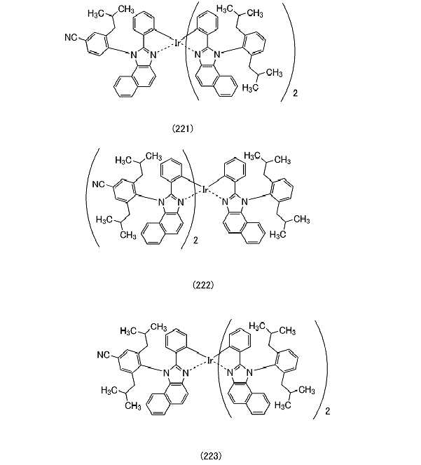
일반식(G-1) 내지 (G-15)로서 나타내어지는 화합물의 구체적인 구조로서는, 하기 구조식(100) 내지 (123) 및 구조식(200) 내지 (223)으로 나타내어지는 유기 금속 착체를 들 수 있다. 또한, 일반식(G-1) 내지 (G-15)로서 나타내어지는 유기 금속 착체는 하기 예시에 한정되지 않는다. Specific structures of the compounds represented by the general formulas (G-1) to (G-15) include organometallic complexes represented by the following structural formulas (100) to (123) and structural formulas (200) to (223). . In addition, the organometallic complex represented by General Formulas (G-1) to (G-15) is not limited to the following examples.
[화학식 39][Chemical Formula 39]

[화학식 40][Formula 40]

[화학식 41][Formula 41]

[화학식 42][Formula 42]

[화학식 43][Formula 43]

[화학식 44][Formula 44]

[화학식 45][Formula 45]
또한, 본 실시형태에서의 유기 금속 착체는 증착법(진공 증착법을 포함함), 잉크젯법, 도포법, 그라비어 인쇄법 등의 방법을 사용하여 성막할 수 있다. In addition, the organometallic complex in this embodiment can be formed using a method such as a vapor deposition method (including a vacuum vapor deposition method), an ink jet method, a coating method, and a gravure printing method.
또한 본 실시형태는 다른 실시형태와 적절히 조합할 수 있다. Further, this embodiment can be appropriately combined with other embodiments.
(실시형태 2)(Embodiment 2)
본 실시형태에서는, 본 발명의 일 형태의 유기 금속 착체의 합성법의 일례에 대하여 설명한다. In this embodiment, an example of a method for synthesizing the organometallic complex of one embodiment of the present invention will be described.
<<일반식(g-1)으로 나타내어지는 1H-나프토[1,2-d]이미다졸 유도체의 합성 방법>><<Synthesis method of 1H-naphtho[1,2-d]imidazole derivative represented by general formula (g-1)>>
하기 일반식(g-1)으로 나타내어지는 1H-나프토[1,2-d]이미다졸 유도체의 합성법의 일례에 대하여 설명한다. 일반식(G-1)으로 나타내어지는 구조를 가지는 본 발명의 일 형태의 유기 금속 착체는 일반식(g-1)으로 나타내어지는 1H-나프토[1,2-d]이미다졸 유도체를 리간드로서 가진다. 따라서, 일반식(g-1)으로 나타내어지는 1H-나프토[1,2-d]이미다졸 유도체를 사용하여 Ir 착체를 합성함으로써, 후술하는 바와 같이, 본 발명의 일 형태의 유기 금속 착체를 합성할 수 있다. An example of a method for synthesizing 1H-naphtho[1,2-d]imidazole derivative represented by the following general formula (g-1) will be described. The organometallic complex of one embodiment of the present invention having a structure represented by the general formula (G-1) is a 1H-naphtho[1,2-d]imidazole derivative represented by the general formula (g-1) as a ligand. Have. Therefore, by synthesizing the Ir complex using the 1H-naphtho[1,2-d]imidazole derivative represented by the general formula (g-1), as described later, an organometallic complex of one embodiment of the present invention can be obtained. It can be synthesized.
[화학식 46][Formula 46]

일반식(g-1) 중에서, R1 내지 R10은 각각 독립적으로 수소, 탄소수 1 내지 6의 알킬기, 치환 또는 비치환된 탄소수 3 내지 7의 사이클로알킬기, 치환 또는 비치환된 탄소수 6 내지 25의 아릴기, 또는 전자 흡인기를 나타내고, Ar는 치환 또는 비치환된 탄소수 6 내지 25의 아릴기를 나타낸다.In the general formula (g-1), R 1 to R 10 are each independently hydrogen, a
하기 스킴(S-1)으로 나타내어진 바와 같이, 아릴알데하이드 화합물 또는 아릴카복실산염화물(M1)과 Ar로 N위치가 치환된 o-나프탈렌다이아민 유도체(M2)의 반응에 의하여, 일반식(g-1)으로 나타내어지는 1H-나프토[1,2-d]이미다졸 유도체를 얻을 수 있다. As represented by the following scheme (S-1), by reaction of an arylaldehyde compound or arylcarboxylic acid chloride (M1) with an o-naphthalenediamine derivative (M2) in which the N position is substituted with Ar, the general formula (g- The 1H-naphtho[1,2-d]imidazole derivative represented by 1) can be obtained.
[화학식 47][Chemical Formula 47]

스킴(S-1)에서, R1 내지 R10은 각각 독립적으로 수소, 탄소수 1 내지 6의 알킬기, 치환 또는 비치환된 탄소수 3 내지 7의 사이클로알킬기, 치환 또는 비치환된 탄소수 6 내지 25의 아릴기, 또는 전자 흡인기를 나타내고, Ar는 치환 또는 비치환된 탄소수 6 내지 25의 아릴기를 나타낸다.In the scheme (S-1), R 1 to R 10 are each independently hydrogen, a
<일반식(G-6)으로 나타내어지는 유기 금속 착체의 합성법><Synthesis method of organometallic complex represented by general formula (G-6)>
다음으로, 일반식(G-1)으로 나타내어지는 구조를 가지는 유기 금속 착체의 합성 방법 중, 일반식(G-6)으로 나타내어지는 유기 금속 착체의 합성법의 일례에 대하여 설명한다. Next, among the methods for synthesizing an organometallic complex having a structure represented by General Formula (G-1), an example of a method for synthesizing an organometallic complex represented by General Formula (G-6) will be described.
하기 스킴(S-2)으로 나타내어진 바와 같이, 일반식(g-1)으로 나타내어지는 1H-나프토[1,2-d]이미다졸 유도체와, 할로젠을 포함하는 이리듐 금속 화합물(염화이리듐 수화물, 헥사클로로이리듐산암모늄 등), 또는 이리듐 유기 금속 착체 화합물(아세틸아세토네이토 착체, 다이에틸설파이드 착체 등)을 혼합한 후, 가열함으로써 일반식(G-6)으로 나타내어지는 구조를 가지는 유기 금속 착체를 얻을 수 있다. 또한, 이 가열 프로세스는 일반식(g-1)으로 나타내어지는 1H-나프토[1,2-d]이미다졸 유도체와, 할로젠을 포함하는 이리듐 금속 화합물, 또는 이리듐 유기 금속 착체를 알코올계 용매(글리세롤, 에틸렌글라이콜, 2-메톡시에탄올, 2-에톡시에탄올 등)에 용해시킨 후에 수행하여도 좋다. 또한, 스킴(S-2)에서, R1 내지 R10은 각각 독립적으로 수소, 탄소수 1 내지 6의 알킬기, 치환 또는 비치환된 탄소수 3 내지 7의 사이클로알킬기, 치환 또는 비치환된 탄소수 6 내지 25의 아릴기, 또는 전자 흡인기를 나타내고, Ar는 치환 또는 비치환된 탄소수 6 내지 25의 아릴기를 나타낸다.As represented by the following scheme (S-2), a 1H-naphtho[1,2-d]imidazole derivative represented by the general formula (g-1) and an iridium metal compound containing halogen (iridium chloride Hydrate, ammonium hexachloroiridate, etc.), or an iridium organometallic complex compound (acetylacetonato complex, diethylsulfide complex, etc.) is mixed and heated to A metal complex can be obtained. In addition, in this heating process, the 1H-naphtho[1,2-d]imidazole derivative represented by the general formula (g-1) and the iridium metal compound containing halogen, or the iridium organometal complex are mixed with an alcohol-based solvent. It may be carried out after dissolving in (glycerol, ethylene glycol, 2-methoxyethanol, 2-ethoxyethanol, etc.). In addition, in the scheme (S-2), R 1 to R 10 are each independently hydrogen, a
[화학식 48][Formula 48]

다만, 본 발명의 유기 금속 착체의 합성법은 스킴(S-2)에 한정되지 않는다. However, the method for synthesizing the organometallic complex of the present invention is not limited to the scheme (S-2).
<일반식(G-11)으로 나타내어지는 유기 금속 착체의 합성법><Synthesis method of organometallic complex represented by general formula (G-11)>
다음으로, 일반식(G-1)으로 나타내어지는 구조를 포함하는 유기 금속 착체의 합성 방법 중, 일반식(G-11)으로 나타내어지는 유기 금속 착체의 합성법의 일례에 대하여 설명한다. Next, an example of a method for synthesizing an organometallic complex represented by the general formula (G-11) among the methods for synthesizing an organometallic complex including a structure represented by the general formula (G-1) will be described.
하기 스킴(S-3)으로 나타내어진 바와 같이, 일반식(g-1)으로 나타내어지는 1H-나프토[1,2-d]이미다졸 유도체 또는 L과, 할로젠을 포함하는 이리듐 화합물(염화이리듐, 브로민화이리듐, 아이오딘화이리듐 등)을 무용매, 알코올계 용매(글리세롤, 에틸렌글라이콜, 2-메톡시에탄올, 2-에톡시에탄올 등) 단독, 또는 알코올계 용매 1종류 이상과 물의 혼합 용매를 사용하여, 불활성 가스 분위기에서 가열함으로써, 할로젠으로 가교된 구조를 가지는 유기 금속 착체의 1종류인, 1H-나프토[1,2-d]이미다졸 유도체의 복핵(複核) 착체(P1) 또는 일가음이온성의 2좌 리간드를 포함하는 복핵 착체(P2)를 얻을 수 있다. 또한, 스킴(S-3)에서, X는 할로젠 원자를 나타내고, R1 내지 R10은 각각 독립적으로 수소, 탄소수 1 내지 6의 알킬기, 치환 또는 비치환된 탄소수 3 내지 7의 사이클로알킬기, 치환 또는 비치환된 탄소수 6 내지 25의 아릴기, 또는 전자 흡인기를 나타내고, Ar는 치환 또는 비치환된 탄소수 6 내지 25의 아릴기를 나타낸다.As represented by the following scheme (S-3), 1H-naphtho[1,2-d]imidazole derivative or L represented by the general formula (g-1) and an iridium compound containing halogen (chloride Iridium, iridium bromide, iridium iodide, etc.)with no solvent, alcohol-based solvent (glycerol, ethylene glycol, 2-methoxyethanol, 2-ethoxyethanol, etc.) alone, or with one or more alcohol-based solvents. Peritoneal complex of 1H-naphtho[1,2-d]imidazole derivative, one type of organometallic complex having a structure crosslinked with halogen by heating in an inert gas atmosphere using a mixed solvent of water (P1) Or a peritoneal complex (P2) containing a monoanionic bidentate ligand can be obtained. In addition, in the scheme (S-3), X represents a halogen atom, and R 1 to R 10 are each independently hydrogen, an alkyl group having 1 to 6 carbon atoms, a substituted or unsubstituted cycloalkyl group having 3 to 7 carbon atoms, and a substituted Or an unsubstituted aryl group having 6 to 25 carbon atoms or an electron withdrawing group, and Ar represents a substituted or unsubstituted aryl group having 6 to 25 carbon atoms.
[화학식 49][Formula 49]

또한, 하기 스킴(S-4)으로 나타내어진 바와 같이, 상술한 합성 스킴(S-3)으로 얻어지는 복핵 착체(P1) 또는 (P2)와, 일반식(g-1)으로 나타내어지는 1H-나프토[1,2-d]이미다졸 유도체 또는 L을 불활성 가스 분위기에서 반응시킴으로써, 일반식(G-11)으로 나타내어지는 본 발명의 일 형태인 유기 금속 착체가 얻어진다. 여기서, 얻어진 유기 금속 착체에 광이나 열을 더 조사하여 더욱 반응시킴으로써 기하 이성질체, 광학 이성질체 등의 이성질체를 얻어도 좋고, 이들도 일반식(G-11)으로 나타내어지는 본 발명의 일 형태인 유기 금속 착체이다. 또한, 스킴(S-4)에서, X는 할로젠 원자를 나타내고, R1 내지 R10은 각각 독립적으로 수소, 탄소수 1 내지 6의 알킬기, 치환 또는 비치환된 탄소수 3 내지 7의 사이클로알킬기, 치환 또는 비치환된 탄소수 6 내지 25의 아릴기, 또는 전자 흡인기를 나타내고, Ar는 치환 또는 비치환된 탄소수 6 내지 25의 아릴기를 나타낸다.In addition, as represented by the following scheme (S-4), the peritoneal complex (P1) or (P2) obtained by the above-described synthetic scheme (S-3), and 1H-naph represented by the general formula (g-1) By reacting a to[1,2-d]imidazole derivative or L in an inert gas atmosphere, an organometallic complex as one embodiment of the present invention represented by the general formula (G-11) is obtained. Here, the obtained organometallic complex may be further reacted with light or heat to obtain isomers such as geometric isomers and optical isomers. It is a complex. In addition, in the scheme (S-4), X represents a halogen atom, and R 1 to R 10 are each independently hydrogen, an alkyl group having 1 to 6 carbon atoms, a substituted or unsubstituted cycloalkyl group having 3 to 7 carbon atoms, and a substituted Or an unsubstituted aryl group having 6 to 25 carbon atoms or an electron withdrawing group, and Ar represents a substituted or unsubstituted aryl group having 6 to 25 carbon atoms.
[화학식 50][Formula 50]

다만, 본 발명의 유기 금속 착체의 합성법은 스킴(S-3) 및 (S-4)에 한정되지 않는다. However, the method for synthesizing the organometallic complex of the present invention is not limited to the schemes (S-3) and (S-4).
(실시형태 3)(Embodiment 3)
본 실시형태에서는, 본 발명의 일 형태인 유기 금속 착체를 가지는 발광 소자에 대하여 도 1을 사용하여 이하에서 설명한다. In this embodiment, a light-emitting element having an organometallic complex which is one embodiment of the present invention will be described below with reference to FIG. 1.
<발광 소자의 구성예 1><Configuration Example 1 of Light-Emitting Element>
우선, 본 발명의 일 형태의 발광 소자의 구성에 대하여, 도 1의 (A), (B), (C)를 사용하여 이하에서 설명한다. First, a configuration of a light emitting device according to an embodiment of the present invention will be described below with reference to FIGS. 1A, 1B, and 1C.
도 1의 (A)는 본 발명의 일 형태의 발광 소자(150)의 단면 모식도이다.
1A is a schematic cross-sectional view of a light-emitting
발광 소자(150)는 한 쌍의 전극(전극(101) 및 전극(102))을 가지고, 상기 한 쌍의 전극 사이에 제공된 EL층(100)을 가진다. EL층(100)은 적어도 발광층(140)을 가진다.
The light-emitting
또한, 도 1의 (A)에 도시된 EL층(100)은 발광층(140) 외에 정공 주입층(111), 정공 수송층(112), 전자 수송층(118), 및 전자 주입층(119) 등의 기능층을 가진다.
In addition, the
또한, 본 실시형태에서는, 한 쌍의 전극 중, 전극(101)을 양극으로서, 전극(102)을 음극으로서 설명하지만, 발광 소자(150)의 구성은 이에 한정되지 않는다. 즉, 전극(101)을 음극으로 하고 전극(102)을 양극으로 하고, 이 전극들 사이의 각 층의 적층을 반대의 순서로 하여도 좋다. 즉, 양극 측으로부터, 정공 주입층(111)과, 정공 수송층(112)과, 발광층(140)과, 전자 수송층(118)과, 전자 주입층(119)이 적층되는 순서로 하면 좋다.
In the present embodiment, of the pair of electrodes, the
또한 EL층(100)의 구성은 도 1의 (A)에 나타내어진 구성에 한정되지 않고, 정공 주입층(111), 정공 수송층(112), 전자 수송층(118), 및 전자 주입층(119) 중에서 선택된 적어도 하나를 가지는 구성으로 하면 좋다. 또는 EL층(100)은 정공 또는 전자의 주입 장벽을 저감할 수 있거나, 정공 또는 전자의 수송성을 향상시킬 수 있거나, 정공 또는 전자의 수송성을 저해할 수 있거나, 또는 전극으로 인한 소광 현상을 억제할 수 있다는 등의 기능을 가지는 기능층을 가지는 구성으로 하여도 좋다. 또한 기능층은 각각 단층이어도 좋고, 복수의 층이 적층된 구성이어도 좋다.
In addition, the configuration of the
발광 소자(150)는 EL층(100)에서의 어느 층에 본 발명의 일 형태에 따른 유기 금속 착체가 포함되어 있으면 좋다. 또한, 상기 유기 금속 착체는 양호한 양자 수율을 가진다. 그러므로, 발광층(140)의 게스트 재료로서 사용함으로써, 발광 효율이 양호한 발광 소자를 얻을 수 있다.
In the
도 1의 (B)는, 도 1의 (A)에 도시된 발광층(140)의 일례를 나타낸 단면 모식도이다. 도 1의 (B)에 도시된 발광층(140)은 호스트 재료(141)와 게스트 재료(142)를 가진다. 또한, 호스트 재료(141)는 단독의 유기 화합물로 구성되어 있어도 좋지만, 유기 화합물(141_1)과 유기 화합물(141_2)을 가지는 co-host계이어도 좋다. 본 발명의 일 형태의 유기 금속 착체는 게스트 재료(142)로서 적합하게 사용할 수 있다.
FIG. 1B is a schematic cross-sectional view showing an example of the
또한, 게스트 재료(142)로서는 발광성의 유기 재료를 사용하면 좋고, 상기 발광성의 유기 재료로서는 형광을 발할 수 있는 재료(이하, 형광 재료라고도 함)나, 인광을 발할 수 있는 재료(이하, 인광 재료라고도 함)를 들 수 있지만, 발광 효율이 높기 때문에 인광 재료가 바람직하다. 그러므로, 본 발명의 일 형태의 유기 금속 착체를 적합하게 사용할 수 있다. 이하의 설명에서는, 게스트 재료(142)로서 인광 재료를 사용하는 구성에 대하여 설명한다. 또한, 게스트 재료(142)를 인광 재료로 바꿔 읽어도 좋다.
In addition, a light-emitting organic material may be used as the
도 1의 (B)에 도시된 바와 같은, 발광층에 유기 화합물(141_1) 및 유기 화합물(141_2)과 같이 2종류의 호스트 재료를 사용하는 경우(co-host계), 일반적으로 2종류의 호스트 재료에는 전자 수송성 재료와 정공 수송성 재료가 1종류씩 사용된다. 이와 같은 구성은 정공 수송층(112)과 발광층(140) 사이의 정공 주입 장벽과 전자 수송층(118)과 발광층(140) 사이의 전자 주입 장벽이 작아지므로, 구동 전압을 저감할 수 있기 때문에 바람직한 구성이다.
As shown in (B) of FIG. 1, in the case of using two types of host materials such as an organic compound 141_1 and an organic compound 141_2 for the light emitting layer (co-host system), generally two types of host materials One type of electron-transporting material and hole-transporting material is used. Such a configuration is a preferable configuration because the hole injection barrier between the
<발광 소자의 발광 기구><Light-emitting mechanism of light-emitting element>
다음으로, 발광층(140)의 발광 기구에 대하여 이하에서 설명한다.
Next, the light emitting mechanism of the
발광층(140)에서의 호스트 재료(141)가 가지는 유기 화합물(141_1) 및 유기 화합물(141_2)은 들뜬 복합체(엑사이플렉스, 엑시플렉스, 또는 Exciplex라고도 함)를 형성하여도 좋다. 이하에서, 유기 화합물(141_1) 및 유기 화합물(141_2)이 들뜬 복합체를 형성하는 경우에 대하여 설명한다.
The organic compound 141_1 and the organic compound 141_2 included in the host material 141 in the
발광층(140)에서의 유기 화합물(141_1)과, 유기 화합물(141_2)과, 게스트 재료(142)의 에너지 준위의 상관을 도 1의 (C)에 도시하였다. 또한, 도 1의 (C)에서의 표기 및 부호는 이하와 같다. 또한, 이하에서는, 유기 화합물(141_1)을 전자 수송성 재료로 하고, 유기 화합물(141_2)을 정공 수송성 재료로 하여 설명한다.
The correlation between the energy levels of the organic compound 141_1, the organic compound 141_2, and the
·Host(141_1): 유기 화합물(141_1)(호스트 재료)Host (141_1): Organic compound (141_1) (host material)
·Host(141_2): 유기 화합물(141_2)(호스트 재료)Host (141_2): Organic compound (141_2) (host material)
·Guest(142): 게스트 재료(142)(인광성 화합물)Guest (142): Guest material 142 (phosphorescent compound)
·SPH1: 유기 화합물(141_1)(호스트 재료)의 S1 준위S PH1 : S1 level of organic compound (141_1) (host material)
·TPH1: 유기 화합물(141_1)(호스트 재료)의 T1 준위T PH1 : T1 level of organic compound (141_1) (host material)
·SPH2: 유기 화합물(141_2)(호스트 재료)의 S1 준위S PH2 : S1 level of organic compound (141_2) (host material)
·TPH2: 유기 화합물(141_2)(호스트 재료)의 T1 준위T PH2 : T1 level of organic compound (141_2) (host material)
·SPG: 게스트 재료(142)(인광성 화합물)의 S1 준위S PG : S1 level of guest material 142 (phosphorescent compound)
·TPG: 게스트 재료(142)(인광성 화합물)의 T1 준위T PG : T1 level of guest material 142 (phosphorescent compound)
·SPE: 들뜬 복합체의 S1 준위S PE : S1 level of the excited complex
·TPE: 들뜬 복합체의 T1 준위·T PE : T1 level of the excited complex
유기 화합물(141_1)과 유기 화합물(141_2)은 들뜬 복합체를 형성하고, 상기 들뜬 복합체의 S1 준위(SPE)와 T1 준위(TPE)는 서로 인접한 에너지 준위가 된다(도 1의 (C) 경로 E1 참조).The organic compound 141_1 and the organic compound 141_2 form an excited complex, and the S1 level (S PE ) and the T1 level (T PE ) of the excited complex become energy levels adjacent to each other ((C) path in FIG. E 1 ).
유기 화합물(141_1)이 전자를, 유기 화합물(141_2)이 정공을 받음으로써 들뜬 복합체를 빠르게 형성한다. 또는, 한쪽이 들뜬 상태가 되면, 다른 쪽과 빠르게 상호 작용함으로써 들뜬 복합체를 형성한다. 따라서, 발광층(140)에서의 여기자의 대부분이 들뜬 복합체로서 존재한다. 들뜬 복합체의 들뜬 에너지 준위(SPE 또는 TPE)는 들뜬 복합체를 형성하는 호스트 재료(유기 화합물(141_1) 및 유기 화합물(141_2))의 S1 준위(SPH1 및 SPH2)보다 낮아지기 때문에, 더 낮은 들뜬 에너지로 호스트 재료(141)의 들뜬 상태를 형성할 수 있게 된다. 이에 의하여, 발광 소자의 구동 전압을 낮출 수 있다. 또한, 유기 화합물(141_1)이 정공을, 유기 화합물(141_2)이 전자를 받음으로써 들뜬 복합체를 형성하여도 좋다.The organic compound 141_1 receives electrons and the organic compound 141_2 receives holes, thereby rapidly forming an excited complex. Alternatively, when one side becomes an excited state, an excited complex is formed by rapidly interacting with the other. Accordingly, most of the excitons in the
그리고, 들뜬 복합체의 (SPE)와 (TPE)의 양쪽의 에너지를 게스트 재료(142)(인광성 화합물)의 T1 준위로 이동시켜 발광이 얻어진다(도 1의 (C) 경로 E2, E3 참조).Then, light emission is obtained by moving the energy of both (S PE ) and (T PE ) of the excited composite to the T1 level of the guest material 142 (phosphorescent compound) (Fig. 1 (C) path E 2 , E 3 ).
또한, 들뜬 복합체의 T1 준위(TPE)는 게스트 재료(142)의 T1 준위(TPG)보다 큰 것이 바람직하다. 이로써, 생성한 들뜬 복합체의 단일항 들뜬 에너지 및 삼중항 들뜬 에너지를 들뜬 복합체의 S1 준위(SPE) 및 T1 준위(TPE)로부터 게스트 재료(142)의 T1 준위(TPG)로 에너지 이동할 수 있다.In addition, it is preferable that the T1 level (T PE ) of the excited composite is greater than the T1 level (T PG) of the guest material 142. As a result, energy can be transferred from the S1 level (S PE ) and T1 level (T PE ) of the excited composite to the T1 level (T PG ) of the
또한, 들뜬 복합체로부터 게스트 재료(142)로 효율적으로 들뜬 에너지를 이동시키기 위해서는, 들뜬 복합체의 T1 준위(TPE)가 들뜬 복합체를 형성하는 각 유기 화합물(유기 화합물(141_1) 및 유기 화합물(141_2))의 T1 준위(TPH1 및 TPH2)와 동등하거나, 더 작은 것이 바람직하다. 이로써, 각 유기 화합물(유기 화합물(141_1) 및 유기 화합물(141_2))에 의한 들뜬 복합체의 삼중항 들뜬 에너지의 퀀칭이 일어나기 어려워지므로, 효율적으로 들뜬 복합체로부터 게스트 재료(142)로 에너지 이동이 발생한다.In addition, in order to efficiently transfer the excited energy from the excited complex to the
또한, 유기 화합물(141_1)과 유기 화합물(141_2)의 조합이 정공 수송성을 가지는 화합물과 전자 수송성을 가지는 화합물의 조합인 경우, 이의 혼합비에 의하여 캐리어 밸런스를 용이하게 제어할 수 있게 된다. 구체적으로는 정공 수송성을 가지는 화합물:전자 수송성을 가지는 화합물=1:9 내지 9:1(중량비)의 범위가 바람직하다. 또한, 이 구성을 가짐으로써, 캐리어 밸런스를 쉽게 제어할 수 있으므로, 캐리어 재결합 영역의 제어도 쉽게 수행할 수 있다. In addition, when the combination of the organic compound 141_1 and the organic compound 141_2 is a combination of a compound having a hole transporting property and a compound having an electron transporting property, the carrier balance can be easily controlled by the mixing ratio thereof. Specifically, the compound having hole transporting property: the compound having electron transporting property is preferably in the range of = 1:9 to 9:1 (weight ratio). Further, by having this configuration, it is possible to easily control the carrier balance, so that the control of the carrier recombination region can also be easily performed.
또한, 상술한 경로 E2, E3의 과정을 본 명세서 등에서 ExTET(Exciplex-Triplet Energy Transfer)라고 부르는 경우가 있다. 환언하면, 발광층(140)은 들뜬 복합체로부터 게스트 재료(142)로의 들뜬 에너지의 공여가 있다. 또한, 이 경우, TPE로부터 SPE로의 역항간 교차 효율이 반드시 높을 필요는 없고, SPE로부터의 발광 양자 수율이 높을 필요도 없기 때문에, 재료를 폭넓게 선택할 수 있다. 또한, ExTET를 이용함으로써, 발광 효율이 양호하고, 구동 전압이 저감된, 신뢰성이 양호한 발광 소자를 얻을 수 있다.In addition, the process of the above-described paths E 2 and E 3 may be referred to as ExTET (Exciplex-Triplet Energy Transfer) in the present specification and the like. In other words, the light-emitting
유기 화합물(141_1)과 유기 화합물(141_2)의 조합은 들뜬 복합체를 형성할 수 있는 조합이면 좋지만, 한쪽이 다른 쪽의 HOMO 준위보다 낮은 HOMO 준위를 가지고, 또한 다른 쪽의 LUMO 준위보다 낮은 LUMO 준위를 가지는 것이 바람직하다. The combination of the organic compound (141_1) and the organic compound (141_2) is good if it is a combination capable of forming an excited complex, but one side has a lower HOMO level than the other's HOMO level, and also has a lower LUMO level than the other's LUMO level. It is desirable to have.
<재료><Material>
다음으로 본 발명의 일 형태에 따른 발광 소자의 구성 요소의 자세한 사항에 대하여 이하에서 설명한다. Next, details of the constituent elements of the light emitting device according to one embodiment of the present invention will be described below.
<<발광층>><<Light-emitting layer>>
발광층(140) 내에서는, 호스트 재료(141)가 중량비로 가장 많이 존재하고, 게스트 재료(142)는 호스트 재료(141) 내에 분산된다. 게스트 재료(142)가 인광성 화합물인 경우, 발광층(140)의 호스트 재료(141)(유기 화합물(141_1) 및 유기 화합물(141_2))의 T1 준위는 발광층(140)의 게스트 재료(게스트 재료(142))의 T1 준위보다 높은 것이 바람직하다.
In the light-emitting
유기 화합물(141_1)로서는, 질소 함유 6원 헤테로 방향족 고리 골격을 가지는 화합물인 것이 바람직하다. 구체적인 예로서는, 피리딘 골격, 다이아진 골격(피라진 골격, 피리미딘 골격, 및 피리다진 골격), 및 트라이아진 골격을 가지는 화합물을 들 수 있다. 이들 염기성을 가지는 질소 함유 헤테로 방향족 고리 골격을 가지는 화합물로서는, 예를 들어 피리딘 유도체, 바이피리딘 유도체, 피리미딘 유도체, 트라이아진 유도체, 퀴녹살린 유도체, 다이벤조퀴녹살린 유도체, 페난트롤린 유도체, 푸린 유도체 등의 화합물을 들 수 있다. 또한, 유기 화합물(141_1)로서는, 정공보다 전자의 수송성이 높은 재료(전자 수송성 재료)를 사용할 수 있고, 1×10⁻⁶cm2/Vs 이상의 전자 이동도를 가지는 재료인 것이 바람직하다.As the organic compound (141_1), it is preferable that it is a compound having a nitrogen-containing 6-membered heteroaromatic ring skeleton. Specific examples include compounds having a pyridine skeleton, a diazine skeleton (pyrazine skeleton, pyrimidine skeleton, and pyridazine skeleton), and a triazine skeleton. Examples of compounds having a nitrogen-containing heteroaromatic ring skeleton having basicity include pyridine derivatives, bipyridine derivatives, pyrimidine derivatives, triazine derivatives, quinoxaline derivatives, dibenzoquinoxaline derivatives, phenanthroline derivatives, and purine derivatives. And the like compounds. Further, as the organic compound 141_1, a material (electron transport material) having higher electron transport properties than holes can be used, and a material having an electron mobility of 1×10 -6 cm 2 /Vs or more is preferable.
구체적으로는, 예를 들어 바소페난트롤린(약칭: Bphen), 바소큐프로인(약칭: BCP) 등의 피리딘 골격을 가지는 헤테로 방향족 고리 화합물이나, 2-[3-(다이벤조싸이오펜-4-일)페닐]다이벤조[f,h]퀴녹살린(약칭: 2mDBTPDBq-II), 2-[3'-(다이벤조싸이오펜-4-일)바이페닐-3-일]다이벤조[f,h]퀴녹살린(약칭: 2mDBTBPDBq-II), 2-[3'-(9H-카바졸-9-일)바이페닐-3-일]다이벤조[f,h]퀴녹살린(약칭: 2mCzBPDBq), 2-[4-(3,6-다이페닐-9H-카바졸-9-일)페닐]다이벤조[f,h]퀴녹살린(약칭: 2CzPDBq-III), 7-[3-(다이벤조싸이오펜-4-일)페닐]다이벤조[f,h]퀴녹살린(약칭: 7mDBTPDBq-II), 및, 6-[3-(다이벤조싸이오펜-4-일)페닐]다이벤조[f,h]퀴녹살린(약칭: 6mDBTPDBq-II), (2-[3-(3,9'-바이-9H-카바졸-9-일)페닐]다이벤조[f,h]퀴녹살린)(약칭: 2mCzCzPDBq), 4,6-비스[3-(페난트렌-9-일)페닐]피리미딘(약칭: 4,6mPnP2Pm), 4,6-비스[3-(4-다이벤조싸이엔일)페닐]피리미딘(약칭: 4,6mDBTP2Pm-II), 4,6-비스[3-(9H-카바졸-9-일)페닐]피리미딘(약칭: 4,6mCzP2Pm) 등의 다이아진 골격을 가지는 헤테로 방향족 고리 화합물이나, 2-{4-[3-(N-페닐-9H-카바졸-3-일)-9H-카바졸-9-일]페닐}-4,6-다이페닐-1,3,5-트라이아진(약칭: PCCzPTzn), 9-[3-(4,6-다이페닐-1,3,5-트라이아진-2-일)페닐]-9'-페닐-2,3'-바이-9H-카바졸(약칭: mPCCzPTzn-02) 등의 트라이아진 골격을 가지는 헤테로 방향족 고리 화합물이나, 3,5-비스[3-(9H-카바졸-9-일)페닐]피리딘(약칭: 35DCzPPy), 1,3,5-트라이[3-(3-피리딜)페닐]벤젠(약칭: TmPyPB) 등의 피리딘 골격을 가지는 헤테로 방향족 고리 화합물도 사용할 수 있다. 상술한 헤테로 방향족 고리 화합물 중에서도, 트라이아진 골격, 다이아진(피리미딘, 피라진, 피리다진) 골격, 또는 피리딘 골격을 가지는 헤테로 방향족 고리 화합물은 안정적이며 신뢰성이 양호하기 때문에 바람직하다. 또한, 상기 골격을 가지는 헤테로 방향족 고리 화합물은 전자 수송성이 높고, 구동 전압 저감에도 기여한다. 또한 폴리(2,5-피리딘다이일)(약칭: PPy), 폴리[(9,9-다이헥실플루오렌-2,7-다이일)-co-(피리딘-3,5-다이일)](약칭: PF-Py), 폴리[(9,9-다이옥틸플루오렌-2,7-다이일)-co-(2,2'-바이피리딘-6,6'-다이일)](약칭: PF-BPy)과 같은 고분자 화합물을 사용할 수도 있다. 여기서 설명한 물질은 주로 1×10⁻⁶cm2/Vs 이상의 전자 이동도를 가지는 물질이다. 또한 정공보다 전자의 수송성이 높은 물질이라면 상기 이외의 물질을 사용하여도 좋다.Specifically, for example, a heteroaromatic ring compound having a pyridine skeleton such as vasophenanthroline (abbreviation: Bphen) and vasocuproin (abbreviation: BCP), and 2-[3-(dibenzothiophene-4) -Yl)phenyl]dibenzo[f,h]quinoxaline (abbreviation: 2mDBTPDBq-II), 2-[3'-(dibenzothiophen-4-yl)biphenyl-3-yl]dibenzo[f, h]quinoxaline (abbreviation: 2mDBTBPDBq-II), 2-[3'-(9H-carbazol-9-yl)biphenyl-3-yl]dibenzo[f,h]quinoxaline (abbreviation: 2mCzBPDBq), 2-[4-(3,6-diphenyl-9H-carbazol-9-yl)phenyl]dibenzo[f,h]quinoxaline (abbreviation: 2CzPDBq-III), 7-[3-(dibenzoyl) Offen-4-yl)phenyl]dibenzo[f,h]quinoxaline (abbreviation: 7mDBTPDBq-II), and 6-[3-(dibenzothiophen-4-yl)phenyl]dibenzo[f,h ]Quinoxaline (abbreviation: 6mDBTPDBq-II), (2-[3-(3,9'-bi-9H-carbazol-9-yl)phenyl]dibenzo[f,h]quinoxaline) (abbreviation: 2mCzCzPDBq ), 4,6-bis[3-(phenanthren-9-yl)phenyl]pyrimidine (abbreviation: 4,6mPnP2Pm), 4,6-bis[3-(4-dibenzothienyl)phenyl]pyrimidine Heteroaromatic rings having a diazine skeleton such as midine (abbreviation: 4,6mDBTP2Pm-II), 4,6-bis[3-(9H-carbazol-9-yl)phenyl]pyrimidine (abbreviation: 4,6mCzP2Pm) Compound or 2-{4-[3-(N-phenyl-9H-carbazol-3-yl)-9H-carbazol-9-yl]phenyl}-4,6-diphenyl-1,3,5 -Triazine (abbreviation: PCCzPTzn), 9-[3-(4,6-diphenyl-1,3,5-triazin-2-yl)phenyl]-9'-phenyl-2,3'-bi- Heteroaromatic cyclic compounds having a triazine skeleton such as 9H-carbazole (abbreviation: mPCCzPTzn-02), or 3,5-bis[3-(9H-carbazol-9-yl)phenyl]pyridine (abbreviation: 35DCzPPy) , 1,3,5-tri[3-(3-pyridyl)phenyl]benzene (abbreviation: TmPyPB) and other heteroaromatic ring compounds having a pyridine skeleton can also be used. Among the above-described heteroaromatic ring compounds, a heteroaromatic ring compound having a triazine skeleton, a diazine (pyrimidine, pyrazine, pyridazine) skeleton, or a pyridine skeleton is preferable because it is stable and has good reliability. In addition, the heteroaromatic ring compound having the above skeleton has high electron transport properties and contributes to a reduction in driving voltage. Also poly(2,5-pyridindiyl) (abbreviation: PPy), poly[(9,9-dihexylfluorene-2,7-diyl)-co-(pyridin-3,5-diyl)] (Abbreviation: PF-Py), poly[(9,9-dioctylfluorene-2,7-diyl)-co-(2,2'-bipyridin-6,6'-diyl)] (abbreviation : Polymer compounds such as PF-BPy) may also be used. The material described here is mainly a material having an electron mobility of 1×10 -6 cm 2 /Vs or more. In addition, materials other than the above may be used as long as the material has higher electron transport properties than holes.
유기 화합물(141_2)로서는, 질소 함유 5원 헤테로 방향족 고리 골격 또는 3급 아민 골격을 가지는 화합물이 바람직하다. 구체적으로는, 피롤 골격 또는 방향족 아민 골격을 가지는 화합물을 들 수 있다. 예를 들어, 인돌 유도체, 카바졸 유도체, 트라이아릴아민 유도체 등이 있다. 또한, 질소 함유 5원 헤테로 방향족 고리 골격으로서는, 이미다졸 골격, 트라이아졸 골격, 및 테트라졸 골격을 들 수 있다. 또한, 유기 화합물(141_2)로서는 전자보다 정공의 수송성이 높은 재료(정공 수송성 재료)를 사용할 수 있고, 1×10⁻⁶cm2/Vs 이상의 정공 이동도를 가지는 재료인 것이 바람직하다. 또한 상기 정공 수송성 재료는 고분자 화합물이어도 좋다.As the organic compound (141_2), a compound having a nitrogen-containing 5-membered heteroaromatic ring skeleton or a tertiary amine skeleton is preferable. Specifically, a compound having a pyrrole skeleton or an aromatic amine skeleton is exemplified. For example, there are indole derivatives, carbazole derivatives, triarylamine derivatives, and the like. Further, examples of the nitrogen-containing 5-membered heteroaromatic ring skeleton include an imidazole skeleton, a triazole skeleton, and a tetrazole skeleton. Further, as the organic compound 141_2, a material having higher hole transport properties than electrons (hole transport material) can be used, and a material having a hole mobility of 1×10 −6 cm 2 /Vs or more is preferable. Further, the hole-transporting material may be a polymer compound.
이들 정공 수송성이 높은 재료로서 구체적으로는, 방향족 아민 화합물로서, N,N'-다이(p-톨릴)-N,N'-다이페닐-p-페닐렌다이아민(약칭: DTDPPA), 4,4'-비스[N-(4-다이페닐아미노페닐)-N-페닐아미노]바이페닐(약칭: DPAB), N,N'-비스{4-[비스(3-메틸페닐)아미노]페닐}-N,N'-다이페닐-(1,1'-바이페닐)-4,4'-다이아민(약칭: DNTPD), 1,3,5-트리스[N-(4-다이페닐아미노페닐)-N-페닐아미노]벤젠(약칭: DPA3B) 등을 들 수 있다. As these materials having high hole transport properties, specifically, as aromatic amine compounds, N,N'-di(p-tolyl)-N,N'-diphenyl-p-phenylenediamine (abbreviation: DTDPPA), 4, 4'-bis[N-(4-diphenylaminophenyl)-N-phenylamino]biphenyl (abbreviation: DPAB), N,N'-bis{4-[bis(3-methylphenyl)amino]phenyl}- N,N'-diphenyl-(1,1'-biphenyl)-4,4'-diamine (abbreviation: DNTPD), 1,3,5-tris[N-(4-diphenylaminophenyl)- N-phenylamino]benzene (abbreviation: DPA3B), etc. are mentioned.
또한, 카바졸 유도체로서는, 구체적으로는 3-[N-(4-다이페닐아미노페닐)-N-페닐아미노]-9-페닐카바졸(약칭: PCzDPA1), 3,6-비스[N-(4-다이페닐아미노페닐)-N-페닐아미노]-9-페닐카바졸(약칭: PCzDPA2), 3,6-비스[N-(4-다이페닐아미노페닐)-N-(1-나프틸)아미노]-9-페닐카바졸(약칭: PCzTPN2), 3-[N-(9-페닐카바졸-3-일)-N-페닐아미노]-9-페닐카바졸(약칭: PCzPCA1), 3,6-비스[N-(9-페닐카바졸-3-일)-N-페닐아미노]-9-페닐카바졸(약칭: PCzPCA2), 3-[N-(1-나프틸)-N-(9-페닐카바졸-3-일)아미노]-9-페닐카바졸(약칭: PCzPCN1) 등을 들 수 있다. In addition, as carbazole derivatives, specifically, 3-[N-(4-diphenylaminophenyl)-N-phenylamino]-9-phenylcarbazole (abbreviation: PCzDPA1), 3,6-bis[N-( 4-diphenylaminophenyl)-N-phenylamino]-9-phenylcarbazole (abbreviation: PCzDPA2), 3,6-bis[N-(4-diphenylaminophenyl)-N-(1-naphthyl) Amino]-9-phenylcarbazole (abbreviation: PCzTPN2), 3-[N-(9-phenylcarbazol-3-yl)-N-phenylamino]-9-phenylcarbazole (abbreviation: PCzPCA1), 3, 6-bis[N-(9-phenylcarbazol-3-yl)-N-phenylamino]-9-phenylcarbazole (abbreviation: PCzPCA2), 3-[N-(1-naphthyl)-N-( 9-phenylcarbazol-3-yl)amino]-9-phenylcarbazole (abbreviation: PCzPCN1), and the like.
또한 카바졸 유도체로서는, 그 외에, 4,4'-다이(N-카바졸릴)바이페닐(약칭: CBP), 1,3,5-트리스[4-(N-카바졸릴)페닐]벤젠(약칭: TCPB), 9-[4-(10-페닐-9-안트릴)페닐]-9H-카바졸(약칭: CzPA), 1,4-비스[4-(N-카바졸릴)페닐]-2,3,5,6-테트라페닐벤젠 등을 사용할 수 있다. In addition, as a carbazole derivative, 4,4'-di(N-carbazolyl)biphenyl (abbreviation: CBP), 1,3,5-tris[4-(N-carbazolyl)phenyl]benzene (abbreviation : TCPB), 9-[4-(10-phenyl-9-anthryl)phenyl]-9H-carbazole (abbreviation: CzPA), 1,4-bis[4-(N-carbazolyl)phenyl]-2 ,3,5,6-tetraphenylbenzene, etc. can be used.
또한, N,N-다이페닐-9-[4-(10-페닐-9-안트릴)페닐]-9H-카바졸-3-아민(약칭: CzA1PA), 4-(10-페닐-9-안트릴)트라이페닐아민(약칭: DPhPA), 4-(9H-카바졸-9-일)-4'-(10-페닐-9-안트릴)트라이페닐아민(약칭: YGAPA), N,9-다이페닐-N-[4-(10-페닐-9-안트릴)페닐]-9H-카바졸-3-아민(약칭: PCAPA), N,9-다이페닐-N-{4-[4-(10-페닐-9-안트릴)페닐]페닐}-9H-카바졸-3-아민(약칭: PCAPBA), N,9-다이페닐-N-(9,10-다이페닐-2-안트릴)-9H-카바졸-3-아민(약칭: 2PCAPA), 9-페닐-3-[4-(10-페닐-9-안트릴)페닐]-9H-카바졸(약칭: PCzPA), 3,6-다이페닐-9-[4-(10-페닐-9-안트릴)페닐]-9H-카바졸(약칭: DPCzPA), N,N,N',N',N'',N'',N''',N'''-옥타페닐다이벤조[g,p]크리센-2,7,10,15-테트라아민(약칭: DBC1) 등을 사용할 수 있다. Further, N,N-diphenyl-9-[4-(10-phenyl-9-anthryl)phenyl]-9H-carbazol-3-amine (abbreviation: CzA1PA), 4-(10-phenyl-9- Anthryl)triphenylamine (abbreviation: DPhPA), 4-(9H-carbazol-9-yl)-4'-(10-phenyl-9-anthryl)triphenylamine (abbreviation: YGAPA), N,9 -Diphenyl-N-[4-(10-phenyl-9-anthryl)phenyl]-9H-carbazol-3-amine (abbreviation: PCAPA), N,9-diphenyl-N-{4-[4 -(10-phenyl-9-anthryl)phenyl]phenyl}-9H-carbazol-3-amine (abbreviation: PCAPBA), N,9-diphenyl-N-(9,10-diphenyl-2-an Tril)-9H-carbazole-3-amine (abbreviation: 2PCAPA), 9-phenyl-3-[4-(10-phenyl-9-anthryl)phenyl]-9H-carbazole (abbreviation: PCzPA), 3 ,6-diphenyl-9-[4-(10-phenyl-9-anthryl)phenyl]-9H-carbazole (abbreviation: DPCzPA), N,N,N',N',N'',N' ',N''',N'''-octaphenyldibenzo[g,p]chrysene-2,7,10,15-tetraamine (abbreviation: DBC1) and the like can be used.
또한 폴리(N-바이닐카바졸)(약칭: PVK)이나 폴리(4-바이닐트라이페닐아민)(약칭: PVTPA), 폴리[N-(4-{N'-[4-(4-다이페닐아미노)페닐]페닐-N'-페닐아미노}페닐)메타크릴아마이드](약칭: PTPDMA), 폴리[N,N'-비스(4-뷰틸페닐)-N,N'-비스(페닐)벤지딘](약칭: Poly-TPD) 등의 고분자 화합물을 사용할 수도 있다. In addition, poly(N-vinylcarbazole) (abbreviation: PVK), poly(4-vinyltriphenylamine) (abbreviation: PVTPA), poly[N-(4-{N'-[4-(4-diphenylamino)” )Phenyl]phenyl-N'-phenylamino}phenyl)methacrylamide] (abbreviation: PTPDMA), poly[N,N'-bis(4-butylphenyl)-N,N'-bis(phenyl)benzidine]( Abbreviation: Poly-TPD) can also be used.
또한, 정공 수송성이 높은 재료로서는, 예를 들어 4,4'-비스[N-(1-나프틸)-N-페닐아미노]바이페닐(약칭: NPB 또는 α-NPD)이나 N,N'-비스(3-메틸페닐)-N,N'-다이페닐-[1,1'-바이페닐]-4,4'-다이아민(약칭: TPD), 4,4',4''-트리스(카바졸-9-일)트라이페닐아민(약칭: TCTA), 4,4',4''-트리스[N-(1-나프틸)-N-페닐아미노]트라이페닐아민(약칭: 1'-TNATA), 4,4',4''-트리스(N,N-다이페닐아미노)트라이페닐아민(약칭: TDATA), 4,4',4''-트리스[N-(3-메틸페닐)-N-페닐아미노]트라이페닐아민(약칭: MTDATA), 4,4'-비스[N-(스파이로-9,9'-바이플루오렌-2-일)-N-페닐아미노]바이페닐(약칭: BSPB), 4-페닐-4'-(9-페닐플루오렌-9-일)트라이페닐아민(약칭: BPAFLP), 4-페닐-3'-(9-페닐플루오렌-9-일)트라이페닐아민(약칭: mBPAFLP), N-(9,9-다이메틸-9H-플루오렌-2-일)-N-{9,9-다이메틸-2-[N'-페닐-N'-(9,9-다이메틸-9H-플루오렌-2-일)아미노]-9H-플루오렌-7-일}페닐아민(약칭: DFLADFL), N-(9,9-다이메틸-2-다이페닐아미노-9H-플루오렌-7-일)다이페닐아민(약칭: DPNF), 2-[N-(4-다이페닐아미노페닐)-N-페닐아미노]스파이로-9,9'-바이플루오렌(약칭: DPASF), 4-페닐-4'-(9-페닐-9H-카바졸-3-일)트라이페닐아민(약칭: PCBA1BP), 4,4'-다이페닐-4''-(9-페닐-9H-카바졸-3-일)트라이페닐아민(약칭: PCBBi1BP), 4-(1-나프틸)-4'-(9-페닐-9H-카바졸-3-일)트라이페닐아민(약칭: PCBANB), 4,4'-다이(1-나프틸)-4''-(9-페닐-9H-카바졸-3-일)트라이페닐아민(약칭: PCBNBB), 4-페닐다이페닐-(9-페닐-9H-카바졸-3-일)아민(약칭: PCA1BP), N,N'-비스(9-페닐카바졸-3-일)-N,N'-다이페닐벤젠-1,3-다이아민(약칭: PCA2B), N,N',N''-트라이페닐-N,N',N''-트리스(9-페닐카바졸-3-일)벤젠-1,3,5-트라이아민(약칭: PCA3B), N-(4-바이페닐)-N-(9,9-다이메틸-9H-플루오렌-2-일)-9-페닐-9H-카바졸-3-아민(약칭: PCBiF), N-(1,1'-바이페닐-4-일)-N-[4-(9-페닐-9H-카바졸-3-일)페닐]-9,9-다이메틸-9H-플루오렌-2-아민(약칭: PCBBiF), 9,9-다이메틸-N-페닐-N-[4-(9-페닐-9H-카바졸-3-일)페닐]플루오렌-2-아민(약칭: PCBAF), N-페닐-N-[4-(9-페닐-9H-카바졸-3-일)페닐]스파이로-9,9'-바이플루오렌-2-아민(약칭: PCBASF), 2-[N-(9-페닐카바졸-3-일)-N-페닐아미노]스파이로-9,9'-바이플루오렌(약칭: PCASF), 2,7-비스[N-(4-다이페닐아미노페닐)-N-페닐아미노]-스파이로-9,9'-바이플루오렌(약칭: DPA2SF), N-[4-(9H-카바졸-9-일)페닐]-N-(4-페닐)페닐아닐린(약칭: YGA1BP), N,N'-비스[4-(카바졸-9-일)페닐]-N,N'-다이페닐-9,9-다이메틸플루오렌-2,7-다이아민(약칭: YGA2F) 등의 방향족 아민 화합물 등을 사용할 수 있다. 또한, 3-[4-(1-나프틸)-페닐]-9-페닐-9H-카바졸(약칭: PCPN), 3-[4-(9-페난트릴)-페닐]-9-페닐-9H-카바졸(약칭: PCPPn), 3,3'-비스(9-페닐-9H-카바졸)(약칭: PCCP), 1,3-비스(N-카바졸릴)벤젠(약칭: mCP), 3,6-비스(3,5-다이페닐페닐)-9-페닐카바졸(약칭: CzTP), 3,6-다이(9H-카바졸-9-일)-9-페닐-9H-카바졸(약칭: PhCzGI), 2,8-다이(9H-카바졸-9-일)-다이벤조싸이오펜(약칭: Cz2DBT) 등의 아민 화합물, 카바졸 화합물 등을 사용할 수 있다. 상술한 화합물 중에서도 피롤 골격, 방향족 아민 골격을 가지는 화합물은 안정적이며 신뢰성이 양호하기 때문에 바람직하다. 또한 상기 골격을 가지는 화합물은 정공 수송성이 높아 구동 전압 저감에도 기여한다. In addition, as a material having high hole transport properties, for example, 4,4'-bis[N-(1-naphthyl)-N-phenylamino]biphenyl (abbreviation: NPB or α-NPD) or N,N'- Bis(3-methylphenyl)-N,N'-diphenyl-[1,1'-biphenyl]-4,4'-diamine (abbreviation: TPD), 4,4',4''-tris (kaba Zol-9-yl)triphenylamine (abbreviation: TCTA), 4,4',4''-tris[N-(1-naphthyl)-N-phenylamino]triphenylamine (abbreviation: 1'-TNATA ), 4,4',4''-tris(N,N-diphenylamino)triphenylamine (abbreviation: TDATA), 4,4',4''-tris[N-(3-methylphenyl)-N -Phenylamino]triphenylamine (abbreviation: MTDATA), 4,4'-bis[N-(spiro-9,9'-bifluoren-2-yl)-N-phenylamino]biphenyl (abbreviation: BSPB), 4-phenyl-4'-(9-phenylfluoren-9-yl)triphenylamine (abbreviation: BPAFLP), 4-phenyl-3'-(9-phenylfluoren-9-yl)triphenyl Amine (abbreviation: mBPAFLP), N-(9,9-dimethyl-9H-fluoren-2-yl)-N-(9,9-dimethyl-2-[N'-phenyl-N'-(9 ,9-dimethyl-9H-fluoren-2-yl)amino]-9H-fluoren-7-yl}phenylamine (abbreviation: DFLADFL), N-(9,9-dimethyl-2-diphenylamino -9H-fluoren-7-yl)diphenylamine (abbreviation: DPNF), 2-[N-(4-diphenylaminophenyl)-N-phenylamino]spiro-9,9'-bifluorene ( Abbreviation: DPASF), 4-phenyl-4'-(9-phenyl-9H-carbazol-3-yl)triphenylamine (abbreviation: PCBA1BP), 4,4'-diphenyl-4''-(9- Phenyl-9H-carbazol-3-yl)triphenylamine (abbreviation: PCBBi1BP), 4-(1-naphthyl)-4'-(9-phenyl-9H-carbazol-3-yl)triphenylamine ( Abbreviation: PCBANB), 4,4'-di(1-naphthyl)-4''-(9-phenyl-9H-carbazol-3-yl) triphenylamine (abbreviation: PCBNBB), 4-phenyldiphenyl -(9-phenyl-9H-carbazol-3-yl)amine (abbreviation: PCA1BP), N,N'-bis(9-phenylcarbazol-3-yl)-N,N'-diphenylbenzene-1 ,3-diamine (abbreviation: PCA2B), N,N',N' '-Triphenyl-N,N',N''-tris(9-phenylcarbazol-3-yl)benzene-1,3,5-triamine (abbreviation: PCA3B), N-(4-biphenyl) -N-(9,9-dimethyl-9H-fluoren-2-yl)-9-phenyl-9H-carbazol-3-amine (abbreviation: PCBiF), N-(1,1'-biphenyl- 4-yl)-N-[4-(9-phenyl-9H-carbazol-3-yl)phenyl]-9,9-dimethyl-9H-fluoren-2-amine (abbreviation: PCBBiF), 9, 9-dimethyl-N-phenyl-N-[4-(9-phenyl-9H-carbazol-3-yl)phenyl]fluoren-2-amine (abbreviation: PCBAF), N-phenyl-N-[4 -(9-phenyl-9H-carbazol-3-yl)phenyl]spiro-9,9'-bifluoren-2-amine (abbreviation: PCBASF), 2-[N-(9-phenylcarbazole- 3-yl)-N-phenylamino]spiro-9,9'-bifluorene (abbreviation: PCASF), 2,7-bis[N-(4-diphenylaminophenyl)-N-phenylamino]- Spiro-9,9'-bifluorene (abbreviation: DPA2SF), N-[4-(9H-carbazol-9-yl)phenyl]-N-(4-phenyl)phenylaniline (abbreviation: YGA1BP), N,N'-bis[4-(carbazol-9-yl)phenyl]-N,N'-diphenyl-9,9-dimethylfluorene-2,7-diamine (abbreviation: YGA2F), etc. An aromatic amine compound or the like can be used. Further, 3-[4-(1-naphthyl)-phenyl]-9-phenyl-9H-carbazole (abbreviation: PCPN), 3-[4-(9-phenanthryl)-phenyl]-9-phenyl- 9H-carbazole (abbreviation: PCPPn), 3,3'-bis (9-phenyl-9H-carbazole) (abbreviation: PCCP), 1,3-bis (N-carbazolyl) benzene (abbreviation: mCP), 3,6-bis(3,5-diphenylphenyl)-9-phenylcarbazole (abbreviation: CzTP), 3,6-di(9H-carbazol-9-yl)-9-phenyl-9H-carbazole Amine compounds, carbazole compounds, such as (abbreviation: PhCzGI) and 2,8-di(9H-carbazol-9-yl)-dibenzothiophene (abbreviation: Cz2DBT) can be used. Among the compounds described above, compounds having a pyrrole skeleton and an aromatic amine skeleton are preferable because they are stable and have good reliability. In addition, the compound having the skeleton has high hole transport properties and contributes to a reduction in driving voltage.
또한, 유기 화합물(141_2)로서는, 이미다졸 골격, 트라이아졸 골격, 및 테트라졸 골격 등의 질소 함유 5원 헤테로 방향족 고리 골격을 가지는 화합물을 사용할 수 있다. 구체적으로는, 예를 들어 3-(4-바이페닐릴)-4-페닐-5-(4-tert-뷰틸페닐)-1,2,4-트라이아졸(약칭: TAZ), 9-[4-(4,5-다이페닐-4H-1,2,4-트라이아졸-3-일)페닐]-9H-카바졸(약칭: CzTAZ1), 2,2',2''-(1,3,5-벤젠트라이일)트리스(1-페닐-1H-벤즈이미다졸)(약칭: TPBI), 2-[3-(다이벤조싸이오펜-4-일)페닐]-1-페닐-1H-벤즈이미다졸(약칭: mDBTBIm-II) 등을 사용할 수 있다. Further, as the organic compound 141_2, a compound having a nitrogen-containing 5-membered heteroaromatic ring skeleton such as an imidazole skeleton, a triazole skeleton, and a tetrazole skeleton can be used. Specifically, for example, 3-(4-biphenylyl)-4-phenyl-5-(4-tert-butylphenyl)-1,2,4-triazole (abbreviation: TAZ), 9-[4 -(4,5-diphenyl-4H-1,2,4-triazol-3-yl)phenyl]-9H-carbazole (abbreviation: CzTAZ1), 2,2',2''-(1,3 ,5-benzenetriyl)tris(1-phenyl-1H-benzimidazole) (abbreviation: TPBI), 2-[3-(dibenzothiophen-4-yl)phenyl]-1-phenyl-1H-benz Imidazole (abbreviation: mDBTBIm-II) or the like can be used.
또한, 발광층(140)에서, 게스트 재료(142)로서는 본 발명의 일 형태의 유기 금속 착체를 적합하게 사용할 수 있다. 본 발명의 일 형태의 유기 금속 착체는 양자 수율이 높기 때문에, 발광 효율이 양호한 발광 소자를 얻을 수 있다. 또한, 후술하는 발광 소자(250)와 같이 복수의 발광 유닛을 가지는 발광 소자의 경우, 하나의 발광 유닛의 발광층에는 본 발명의 일 형태의 유기 화합물을 사용하는 것이 바람직하다. 다른 발광 유닛에 사용하는 게스트 재료에는 특별히 한정은 없지만, 형광성 화합물로서는 안트라센 유도체, 테트라센 유도체, 크리센 유도체, 페난트렌 유도체, 피렌 유도체, 페릴렌 유도체, 스틸벤 유도체, 아크리돈 유도체, 쿠마린 유도체, 페녹사진 유도체, 페노싸이아진 유도체 등이 바람직하고, 예를 들어 이하의 물질을 사용할 수 있다.
In addition, in the
구체적으로는, 5,6-비스[4-(10-페닐-9-안트릴)페닐]-2,2'-바이피리딘(약칭: PAP2BPy), 5,6-비스[4'-(10-페닐-9-안트릴)바이페닐-4-일]-2,2'-바이피리딘(약칭: PAPP2BPy), N,N'-다이페닐-N,N'-비스[4-(9-페닐-9H-플루오렌-9-일)페닐]피렌-1,6-다이아민(약칭: 1,6FLPAPrn), N,N'-비스(3-메틸페닐)-N,N'-비스[3-(9-페닐-9H-플루오렌-9-일)페닐]피렌-1,6-다이아민(약칭: 1,6mMemFLPAPrn), N,N'-비스[4-(9-페닐-9H-플루오렌-9-일)페닐]-N,N'-비스(4-tert-뷰틸페닐)피렌-1,6-다이아민(약칭: 1,6tBu-FLPAPrn), N,N'-다이페닐-N,N'-비스[4-(9-페닐-9H-플루오렌-9-일)페닐]-3,8-다이사이클로헥실피렌-1,6-다이아민(약칭: ch-1,6FLPAPrn), N,N'-비스[4-(9H-카바졸-9-일)페닐]-N,N'-다이페닐스틸벤-4,4'-다이아민(약칭: YGA2S), 4-(9H-카바졸-9-일)-4'-(10-페닐-9-안트릴)트라이페닐아민(약칭: YGAPA), 4-(9H-카바졸-9-일)-4'-(9,10-다이페닐-2-안트릴)트라이페닐아민(약칭: 2YGAPPA), N,9-다이페닐-N-[4-(10-페닐-9-안트릴)페닐]-9H-카바졸-3-아민(약칭: PCAPA), 페릴렌, 2,5,8,11-테트라(tert-뷰틸)페릴렌(약칭: TBP), 4-(10-페닐-9-안트릴)-4'-(9-페닐-9H-카바졸-3-일)트라이페닐아민(약칭: PCBAPA), N,N''-(2-tert-뷰틸안트라센-9,10-다이일다이-4,1-페닐렌)비스[N,N',N'-트라이페닐-1,4-페닐렌다이아민](약칭: DPABPA), N,9-다이페닐-N-[4-(9,10-다이페닐-2-안트릴)페닐]-9H-카바졸-3-아민(약칭: 2PCAPPA), N-[4-(9,10-다이페닐-2-안트릴)페닐]-N,N',N'-트라이페닐-1,4-페닐렌다이아민(약칭: 2DPAPPA), N,N,N',N',N'',N'',N''',N'''-옥타페닐다이벤조[g,p]크리센-2,7,10,15-테트라아민(약칭: DBC1), 쿠마린30, N-(9,10-다이페닐-2-안트릴)-N,9-다이페닐-9H-카바졸-3-아민(약칭: 2PCAPA), N-[9,10-비스(1,1'-바이페닐-2-일)-2-안트릴]-N,9-다이페닐-9H-카바졸-3-아민(약칭: 2PCABPhA), N-(9,10-다이페닐-2-안트릴)-N,N',N'-트라이페닐-1,4-페닐렌다이아민(약칭: 2DPAPA), N-[9,10-비스(1,1'-바이페닐-2-일)-2-안트릴]-N,N',N'-트라이페닐-1,4-페닐렌다이아민(약칭: 2DPABPhA), 9,10-비스(1,1'-바이페닐-2-일)-N-[4-(9H-카바졸-9-일)페닐]-N-페닐안트라센-2-아민(약칭: 2YGABPhA), N,N,9-트라이페닐안트라센-9-아민(약칭: DPhAPhA), 쿠마린6, 쿠마린545T, N,N'-다이페닐퀴나크리돈(약칭: DPQd), 루브렌, 2,8-다이-tert-뷰틸-5,11-비스(4-tert-뷰틸페닐)-6,12-다이페닐테트라센(약칭: TBRb), 나일레드, 5,12-비스(1,1'-바이페닐-4-일)-6,11-다이페닐테트라센(약칭: BPT), 2-(2-{2-[4-(다이메틸아미노)페닐]에텐일}-6-메틸-4H-피란-4-일리덴)프로페인다이나이트릴(약칭: DCM1), 2-{2-메틸-6-[2-(2,3,6,7-테트라하이드로-1H,5H-벤조[ij]퀴놀리진-9-일)에텐일]-4H-피란-4-일리덴}프로페인다이나이트릴(약칭: DCM2), N,N,N',N'-테트라키스(4-메틸페닐)테트라센-5,11-다이아민(약칭: p-mPhTD), 7,14-다이페닐-N,N,N',N'-테트라키스(4-메틸페닐)아세나프토[1,2-a]플루오란텐-3,10-다이아민(약칭: p-mPhAFD), 2-{2-아이소프로필-6-[2-(1,1,7,7-테트라메틸-2,3,6,7-테트라하이드로-1H,5H-벤조[ij]퀴놀리진-9-일)에텐일]-4H-피란-4-일리덴}프로페인다이나이트릴(약칭: DCJTI), 2-{2-tert-뷰틸-6-[2-(1,1,7,7-테트라메틸-2,3,6,7-테트라하이드로-1H,5H-벤조[ij]퀴놀리진-9-일)에텐일]-4H-피란-4-일리덴}프로페인다이나이트릴(약칭: DCJTB), 2-(2,6-비스{2-[4-(다이메틸아미노)페닐]에텐일}-4H-피란-4-일리덴)프로페인다이나이트릴(약칭: BisDCM), 2-{2,6-비스[2-(8-메톡시-1,1,7,7-테트라메틸-2,3,6,7-테트라하이드로-1H,5H-벤조[ij]퀴놀리진-9-일)에텐일]-4H-피란-4-일리덴}프로페인다이나이트릴(약칭: BisDCJTM), 5,10,15,20-테트라페닐비스벤조[5,6]인데노[1,2,3-cd:1',2',3'-lm]페릴렌 등을 들 수 있다. Specifically, 5,6-bis[4-(10-phenyl-9-anthryl)phenyl]-2,2'-bipyridine (abbreviation: PAP2BPy), 5,6-bis[4'-(10- Phenyl-9-anthryl)biphenyl-4-yl]-2,2'-bipyridine (abbreviation: PAPP2BPy), N,N'-diphenyl-N,N'-bis[4-(9-phenyl-) 9H-fluoren-9-yl)phenyl]pyrene-1,6-diamine (abbreviation: 1,6FLPAPrn), N,N'-bis(3-methylphenyl)-N,N'-bis[3-(9 -Phenyl-9H-fluoren-9-yl)phenyl]pyrene-1,6-diamine (abbreviation: 1,6mMemFLPAPrn), N,N'-bis[4-(9-phenyl-9H-fluorene-9) -Yl)phenyl]-N,N'-bis(4-tert-butylphenyl)pyrene-1,6-diamine (abbreviation: 1,6tBu-FLPAPrn), N,N'-diphenyl-N,N' -Bis[4-(9-phenyl-9H-fluoren-9-yl)phenyl]-3,8-dicyclohexylpyrene-1,6-diamine (abbreviation: ch-1,6FLPAPrn), N,N '-Bis[4-(9H-carbazol-9-yl)phenyl]-N,N'-diphenylstilbene-4,4'-diamine (abbreviation: YGA2S), 4-(9H-carbazole- 9-yl)-4'-(10-phenyl-9-anthryl)triphenylamine (abbreviation: YGAPA), 4-(9H-carbazol-9-yl)-4'-(9,10-diphenyl -2-Anthryl)triphenylamine (abbreviation: 2YGAPPA), N,9-diphenyl-N-[4-(10-phenyl-9-anthryl)phenyl]-9H-carbazole-3-amine (abbreviation : PCAPA), perylene, 2,5,8,11-tetra(tert-butyl)perylene (abbreviation: TBP), 4-(10-phenyl-9-anthryl)-4'-(9-phenyl-) 9H-carbazol-3-yl)triphenylamine (abbreviation: PCBAPA), N,N''-(2-tert-butylanthracene-9,10-diyldi-4,1-phenylene)bis[N ,N',N'-triphenyl-1,4-phenylenediamine] (abbreviation: DPABPA), N,9-diphenyl-N-[4-(9,10-diphenyl-2-anthryl) Phenyl]-9H-carbazol-3-amine (abbreviation: 2PCAPPA), N-[4-(9,10-diphenyl-2-anthryl)phenyl]-N,N',N'-triphenyl-1 ,4-phenylenediamine (abbreviation: 2DPAPPA), N,N,N',N',N'',N'',N''',N'''-octa Phenyldibenzo[g,p]chrysene-2,7,10,15-tetraamine (abbreviation: DBC1), coumarin 30, N-(9,10-diphenyl-2-anthryl)-N,9- Diphenyl-9H-carbazol-3-amine (abbreviation: 2PCAPA), N-[9,10-bis(1,1'-biphenyl-2-yl)-2-anthryl]-N,9-di Phenyl-9H-carbazol-3-amine (abbreviation: 2PCABPhA), N-(9,10-diphenyl-2-anthryl)-N,N',N'-triphenyl-1,4-phenylenedia Min (abbreviation: 2DPAPA), N-[9,10-bis(1,1'-biphenyl-2-yl)-2-anthryl]-N,N',N'-triphenyl-1,4- Phenylenediamine (abbreviation: 2DPABPhA), 9,10-bis(1,1'-biphenyl-2-yl)-N-[4-(9H-carbazol-9-yl)phenyl]-N-phenyl Anthracene-2-amine (abbreviation: 2YGABPhA), N,N,9-triphenylanthracene-9-amine (abbreviation: DPhAPhA), coumarin 6, coumarin 545T, N,N'-diphenylquinacridone (abbreviation: DPQd ), rubrene, 2,8-di-tert-butyl-5,11-bis(4-tert-butylphenyl)-6,12-diphenyltetracene (abbreviation: TBRb), nile red, 5,12- Bis(1,1'-biphenyl-4-yl)-6,11-diphenyltetracene (abbreviation: BPT), 2-(2-{2-[4-(dimethylamino)phenyl]ethenyl} -6-Methyl-4H-pyran-4-ylidene) propaneinitryl (abbreviation: DCM1), 2-{2-methyl-6-[2-(2,3,6,7-tetrahydro-1H) ,5H-benzo[ij]quinolizin-9-yl)ethenyl]-4H-pyran-4-ylidene}propane initril (abbreviation: DCM2), N,N,N',N'-tetra Kis(4-methylphenyl)tetracene-5,11-diamine (abbreviation: p-mPhTD), 7,14-diphenyl-N,N,N',N'-tetrakis(4-methylphenyl)acenaphtho [1,2-a]Fluoranthene-3,10-diamine (abbreviation: p-mPhAFD), 2-{2-isopropyl-6-[2-(1,1,7,7-tetramethyl-) 2,3,6,7-tetrahydro-1H,5H-benzo[ij]quinolizin-9-yl)ethenyl]-4H-pyran-4-ylidene}propaneinitril (abbreviation: DCJTI) , 2-{2-tert-butyl-6-[2-(1,1,7,7-tetramethyl- 2,3,6,7-tetrahydro-1H,5H-benzo[ij]quinolizin-9-yl)ethenyl]-4H-pyran-4-ylidene}propaneinitril (abbreviation: DCJTB) , 2-(2,6-bis{2-[4-(dimethylamino)phenyl]ethenyl}-4H-pyran-4-ylidene)propaneinitryl (abbreviation: BisDCM), 2-{2 ,6-bis[2-(8-methoxy-1,1,7,7-tetramethyl-2,3,6,7-tetrahydro-1H,5H-benzo[ij]quinolizin-9-yl )Ethenyl]-4H-pyran-4-ylidene}propaininithryl (abbreviation: BisDCJTM), 5,10,15,20-tetraphenylbisbenzo[5,6]indeno[1,2,3 -cd: 1', 2', 3'-lm] perylene, etc. are mentioned.
게스트 재료로서 사용할 수 있는 인광성 화합물로서는, 이리듐, 로듐, 또는 백금계의 유기 금속 착체, 또는 금속 착체를 들 수 있고, 이들 중에서도 유기 이리듐 착체, 예를 들어 이리듐계 오쏘 메탈 착체가 바람직하다. 오쏘 금속화하는 리간드로서는 4H-트라이아졸 리간드, 1H-트라이아졸 리간드, 이미다졸 리간드, 피리딘 리간드, 피리미딘 리간드, 피라진 리간드, 또는 아이소퀴놀린 리간드 등을 들 수 있다. 금속 착체로서는, 포르피린 리간드를 가지는 백금 착체 등을 들 수 있다. Examples of the phosphorescent compound that can be used as a guest material include iridium, rhodium, or platinum-based organometallic complexes or metal complexes, and among these, organic iridium complexes, for example, iridium-based orthometallic complexes are preferable. Examples of the ortho-metallized ligand include 4H-triazole ligand, 1H-triazole ligand, imidazole ligand, pyridine ligand, pyrimidine ligand, pyrazine ligand, or isoquinoline ligand. Examples of the metal complex include a platinum complex having a porphyrin ligand.
청색 또는 녹색에 발광 피크를 가지는 물질로서는, 예를 들어 트리스{2-[5-(2-메틸페닐)-4-(2,6-다이메틸페닐)-4H-1,2,4-트라이아졸-3-일-κN2]페닐-κC}이리듐(III)(약칭: [Ir(mpptz-dmp)3]), 트리스(5-메틸-3,4-다이페닐-4H-1,2,4-트라이아졸레이토)이리듐(III)(약칭: [Ir(Mptz)3]), 트리스[4-(3-바이페닐)-5-아이소프로필-3-페닐-4H-1,2,4-트라이아졸레이토]이리듐(III)(약칭: [Ir(iPrptz-3b)3]), 트리스[3-(5-바이페닐)-5-아이소프로필-4-페닐-4H-1,2,4-트라이아졸레이토]이리듐(III)(약칭: [Ir(iPr5btz)3])과 같은 4H-트라이아졸 골격을 가지는 유기 금속 이리듐 착체나, 트리스[3-메틸-1-(2-메틸페닐)-5-페닐-1H-1,2,4-트라이아졸레이토]이리듐(III)(약칭: [Ir(Mptz1-mp)3]), 트리스(1-메틸-5-페닐-3-프로필-1H-1,2,4-트라이아졸레이토)이리듐(III)(약칭: [Ir(Prptz1-Me)3])과 같은 1H-트라이아졸 골격을 가지는 유기 금속 이리듐 착체나, fac-트리스[1-(2,6-다이아이소프로필페닐)-2-페닐-1H-이미다졸]이리듐(III)(약칭: [Ir(iPrpmi)3]), 트리스[3-(2,6-다이메틸페닐)-7-메틸이미다조[1,2-f]페난트리디네이토]이리듐(III)(약칭: [Ir(dmpimpt-Me)3])과 같은 이미다졸 골격을 가지는 유기 금속 이리듐 착체나, 비스[2-(4',6'-다이플루오로페닐)피리디네이토-N,C2']이리듐(III)테트라키스(1-피라졸릴)보레이트(약칭: FIr6), 비스[2-(4',6'-다이플루오로페닐)피리디네이토-N,C2']이리듐(III)피콜리네이트(약칭: FIrpic), 비스{2-[3',5'-비스(트라이플루오로메틸)페닐]피리디네이토-N,C2'}이리듐(III)피콜리네이트(약칭: [Ir(CF3ppy)2(pic)]), 비스[2-(4',6'-다이플루오로페닐)피리디네이토-N,C2']이리듐(III)아세틸아세토네이트(약칭: [FIr(acac)])와 같은 전자 흡인기를 가지는 페닐피리딘 유도체를 리간드로 하는 유기 금속 이리듐 착체를 들 수 있다. 상기 중에서도, 4H-트라이아졸 골격, 1H-트라이아졸 골격, 및 이미다졸 골격과 같은 질소 함유 5원 헤테로 방향족 고리 골격을 가지는 유기 금속 이리듐 착체는 높은 삼중항 들뜬 에너지를 가지고, 신뢰성이나 발광 효율도 우수하기 때문에 특히 바람직하다.As a substance having an emission peak in blue or green, for example, tris(2-[5-(2-methylphenyl)-4-(2,6-dimethylphenyl)-4H-1,2,4-triazole-3 -Yl-κN2]phenyl-κC}iridium(III) (abbreviation: [Ir(mpptz-dmp) 3 ]), tris(5-methyl-3,4-diphenyl-4H-1,2,4-triazole Leito) iridium (III) (abbreviation: [Ir(Mptz) 3 ]), tris[4-(3-biphenyl)-5-isopropyl-3-phenyl-4H-1,2,4-triazolato] Iridium (III) (abbreviation: [Ir(iPrptz-3b) 3 ]), tris[3-(5-biphenyl)-5-isopropyl-4-phenyl-4H-1,2,4-triazolato] Organometallic iridium complex having a 4H-triazole skeleton such as iridium (III) (abbreviation: [Ir(iPr5btz) 3 ]), or tris[3-methyl-1-(2-methylphenyl)-5-phenyl-1H- 1,2,4-triazolato]iridium(III) (abbreviation: [Ir(Mptz1-mp) 3 ]), tris(1-methyl-5-phenyl-3-propyl-1H-1,2,4- Organometallic iridium complex having a 1H-triazole skeleton such as triazolato) iridium (III) (abbreviation: [Ir(Prptz1-Me) 3 ]), or fac-tris[1-(2,6-diisopropyl) Phenyl)-2-phenyl-1H-imidazole]iridium(III) (abbreviation: [Ir(iPrpmi) 3 ]), tris[3-(2,6-dimethylphenyl)-7-methylimidazo[1, Organometallic iridium complex having an imidazole skeleton such as 2-f]phenanthridineto]iridium(III) (abbreviation: [Ir(dmpimpt-Me) 3 ]), or bis[2-(4',6') -Difluorophenyl)pyridinato-N,C 2' ]Iridium(III)tetrakis(1-pyrazolyl)borate (abbreviation: FIr6), bis[2-(4',6'-difluoro Phenyl)pyridinato-N,C 2' ]iridium(III)picolinate (abbreviation: FIrpic), bis{2-[3',5'-bis(trifluoromethyl)phenyl]pyridinato -N,C 2' }Iridium(III) picolinate (abbreviation: [Ir(CF 3 ppy) 2 (pic)]), bis[2-(4',6'-difluorophenyl)pyri And organometallic iridium complexes having a phenylpyridine derivative having an electron withdrawing group such as dinato-N,C 2′ ]iridium(III)acetylacetonate (abbreviation: [FIr(acac)]) as a ligand. Among the above, organometallic iridium complexes having a nitrogen-containing 5-membered heteroaromatic ring skeleton such as a 4H-triazole skeleton, a 1H-triazole skeleton, and an imidazole skeleton have high triplet excitation energy, and are excellent in reliability and luminous efficiency. Therefore, it is particularly preferable.
또한, 녹색 또는 황색에 발광 피크를 가지는 물질로서는, 예를 들어 트리스(4-메틸-6-페닐피리미디네이토)이리듐(III)(약칭: [Ir(mppm)3]), 트리스(4-t-뷰틸-6-페닐피리미디네이토)이리듐(III)(약칭: [Ir(tBuppm)3]), (아세틸아세토네이토)비스(6-메틸-4-페닐피리미디네이토)이리듐(III)(약칭: [Ir(mppm)2(acac)]), (아세틸아세토네이토)비스(6-tert-뷰틸-4-페닐피리미디네이토)이리듐(III)(약칭: [Ir(tBuppm)2(acac)]), (아세틸아세토네이토)비스[4-(2-노보닐)-6-페닐피리미디네이토]이리듐(III)(약칭: [Ir(nbppm)2(acac)]), (아세틸아세토네이토)비스[5-메틸-6-(2-메틸페닐)-4-페닐피리미디네이토]이리듐(III)(약칭: [Ir(mpmppm)2(acac)]), (아세틸아세토네이토)비스{4,6-다이메틸-2-[6-(2,6-다이메틸페닐)-4-피리미딘일-κN3]페닐-κC}이리듐(III)(약칭: [Ir(dmppm-dmp)2(acac)]), (아세틸아세토네이토)비스(4,6-다이페닐피리미디네이토)이리듐(III)(약칭: [Ir(dppm)2(acac)])과 같은 피리미딘 골격을 가지는 유기 금속 이리듐 착체나, (아세틸아세토네이토)비스(3,5-다이메틸-2-페닐피라지네이토)이리듐(III)(약칭: [Ir(mppr-Me)2(acac)]), (아세틸아세토네이토)비스(5-아이소프로필-3-메틸-2-페닐피라지네이토)이리듐(III)(약칭: [Ir(mppr-iPr)2(acac)])과 같은 피라진 골격을 가지는 유기 금속 이리듐 착체나, 트리스(2-페닐피리디네이토-N,C2')이리듐(III)(약칭: [Ir(ppy)3]), 비스(2-페닐피리디네이토-N,C2')이리듐(III)아세틸아세토네이트(약칭: [Ir(ppy)2(acac)]), 비스(벤조[h]퀴놀리네이토)이리듐(III)아세틸아세토네이트(약칭: [Ir(bzq)2(acac)]), 트리스(벤조[h]퀴놀리네이토)이리듐(III)(약칭: [Ir(bzq)3]), 트리스(2-페닐퀴놀리네이토-N,C2')이리듐(III)(약칭: [Ir(pq)3]), 비스(2-페닐퀴놀리네이토-N,C2')이리듐(III)아세틸아세토네이트(약칭: [Ir(pq)2(acac)])와 같은 피리딘 골격을 가지는 유기 금속 이리듐 착체나, 비스(2,4-다이페닐-1,3-옥사졸레이토-N,C2')이리듐(III)아세틸아세토네이트(약칭: [Ir(dpo)2(acac)]), 비스{2-[4'-(퍼플루오로페닐)페닐]피리디네이토-N,C2'}이리듐(III)아세틸아세토네이트(약칭: [Ir(p-PF-ph)2(acac)]), 비스(2-페닐벤조싸이아졸레이토-N,C2')이리듐(III)아세틸아세토네이트(약칭: [Ir(bt)2(acac)]) 등의 유기 금속 이리듐 착체 외에, 트리스(아세틸아세토네이토)(모노페난트롤린)터븀(III)(약칭: [Tb(acac)3(Phen)])과 같은 희토류 금속 착체를 들 수 있다. 상술한 것 중에서도, 피리미딘 골격을 가지는 유기 금속 이리듐 착체는 신뢰성이나 발광 효율도 매우 우수하여 특히 바람직하다.In addition, as a substance having an emission peak in green or yellow, for example, tris (4-methyl-6-phenylpyrimidinato) iridium (III) (abbreviation: [Ir (mppm) 3 ]), tris (4- t-butyl-6-phenylpyrimidinato) iridium (III) (abbreviation: [Ir (tBuppm) 3 ]), (acetylacetonato) bis (6-methyl-4-phenylpyrimidinato) iridium ( III) (abbreviation: [Ir(mppm) 2 (acac)]), (acetylacetonato) bis(6-tert-butyl-4-phenylpyrimidinato) iridium (III) (abbreviation: [Ir(tBuppm) ) 2 (acac)]), (acetylacetonato) bis[4-(2-norbornyl)-6-phenylpyrimidinato]iridium(III) (abbreviation: [Ir(nbppm) 2 (acac)] ), (acetylacetonato)bis[5-methyl-6-(2-methylphenyl)-4-phenylpyrimidinato]iridium(III) (abbreviation: [Ir(mpmppm) 2 (acac)]), ( Acetylacetonato)bis{4,6-dimethyl-2-[6-(2,6-dimethylphenyl)-4-pyrimidinyl-κN3]phenyl-κC}iridium(III) (abbreviation: [Ir( dmppm-dmp) 2 (acac)]), (acetylacetonato) bis (4,6-diphenylpyrimidinato) iridium (III) (abbreviation: [Ir(dppm) 2 (acac)]) Organometallic iridium complex having a pyrimidine skeleton, (acetylacetonato) bis(3,5-dimethyl-2-phenylpyrazinato) iridium (III) (abbreviation: [Ir(mppr-Me) 2 (acac )]), (acetylacetonato)bis(5-isopropyl-3-methyl-2-phenylpyrazinato)iridium(III) (abbreviation: [Ir(mppr-iPr) 2 (acac)]) Organometallic iridium complex having a pyrazine skeleton, tris(2-phenylpyridinato-N,C 2' ) iridium(III) (abbreviation: [Ir(ppy) 3 ]), bis(2-phenylpyridine) To-N,C 2' )Iridium(III)acetylacetonate (abbreviation: [Ir(ppy) 2 (acac)]), bis(benzo[h]quinolinato)iridium(III)acetylacetonate (abbreviation : [Ir(bzq) 2 (acac)]), tris(benzo[h]quinolinato)iridium (III) (abbreviation: [Ir(bzq) 3 ]), tris(2- phenylquinolinato-N,C 2' ) iridium (III) (abbreviation: [Ir(pq) 3 ]), bis(2 -Phenylquinolinato-N,C 2' ) Iridium (III) acetylacetonate (abbreviation: [Ir(pq) 2 (acac)]), an organometallic iridium complex having the same pyridine skeleton, or bis(2, 4-diphenyl-1,3-oxazolato-N,C 2' ) iridium (III) acetylacetonate (abbreviation: [Ir(dpo) 2 (acac)]), bis {2-[4'-( Perfluorophenyl)phenyl]pyridinato-N,C 2′ }Iridium(III)acetylacetonate (abbreviation: [Ir(p-PF-ph) 2 (acac)]), bis(2-phenylbenzo In addition to organometallic iridium complexes such as thiazolato-N,C 2′ ) iridium (III) acetylacetonate (abbreviation: [Ir(bt) 2 (acac)]), tris (acetylacetonato) (monophenanthrol And rare earth metal complexes such as lean) terbium (III) (abbreviation: [Tb(acac) 3 (Phen)]). Among the above, the organometallic iridium complex having a pyrimidine skeleton is particularly preferable because of its excellent reliability and luminous efficiency.
또한, 황색 또는 적색에 발광 피크를 가지는 물질로서는, 예를 들어 (다이아이소뷰티릴메타네이토)비스[4,6-비스(3-메틸페닐)피리미디네이토]이리듐(III)(약칭: [Ir(5mdppm)2(dibm)]), 비스[4,6-비스(3-메틸페닐)피리미디네이토](다이피발로일메타네이토)이리듐(III)(약칭: [Ir(5mdppm)2(dpm)]), 비스[4,6-다이(나프탈렌-1-일)피리미디네이토](다이피발로일메타네이토)이리듐(III)(약칭: [Ir(d1npm)2(dpm)])과 같은 피리미딘 골격을 가지는 유기 금속 이리듐 착체나, (아세틸아세토네이토)비스(2,3,5-트라이페닐피라지네이토)이리듐(III)(약칭: [Ir(tppr)2(acac)]), 비스(2,3,5-트라이페닐피라지네이토)(다이피발로일메타네이토)이리듐(III)(약칭: Ir(tppr)2(dpm)), (아세틸아세토네이토)비스[2,3-비스(4-플루오로페닐)퀴녹살리네이토]이리듐(III)(약칭: [Ir(Fdpq)2(acac)])과 같은 피라진 골격을 가지는 유기 금속 이리듐 착체나, 트리스(1-페닐아이소퀴놀리네이토-N,C2')이리듐(III)(약칭: [Ir(piq)3]), 비스(1-페닐아이소퀴놀리네이토-N,C2')이리듐(III)아세틸아세토네이트(약칭: [Ir(piq)2(acac)])와 같은 피리딘 골격을 가지는 유기 금속 이리듐 착체 외에, 2,3,7,8,12,13,17,18-옥타에틸-21H,23H-포르피린백금(II)(약칭: [PtOEP])과 같은 백금 착체나, 트리스(1,3-다이페닐-1,3-프로페인다이오네이토)(모노페난트롤린)유로퓸(III)(약칭: [Eu(DBM)3(Phen)]), 트리스[1-(2-테노일)-3,3,3-트라이플루오로아세토네이토](모노페난트롤린)유로퓸(III)(약칭: [Eu(TTA)3(Phen)])과 같은 희토류 금속 착체를 들 수 있다. 상술한 것 중에서도, 피리미딘 골격을 가지는 유기 금속 이리듐 착체는 신뢰성이나 발광 효율도 매우 우수하여 특히 바람직하다. 또한, 피라진 골격을 가지는 유기 금속 이리듐 착체는, 색도가 양호한 적색 발광이 얻어진다.In addition, as a substance having an emission peak in yellow or red, for example (diisobutyrylmethanato)bis[4,6-bis(3-methylphenyl)pyrimidinato]iridium(III) (abbreviation: [ Ir(5mdppm) 2 (dibm)]), bis[4,6-bis(3-methylphenyl)pyrimidinato](dipivaloylmethanato)iridium(III) (abbreviation: [Ir(5mdppm) 2 (dpm)]), bis[4,6-di(naphthalen-1-yl)pyrimidinato](dipivaloylmethanato)iridium(III) (abbreviation: [Ir(d1npm) 2 (dpm) ]) or an organometallic iridium complex having the same pyrimidine skeleton, or (acetylacetonato)bis(2,3,5-triphenylpyrazinato)iridium(III) (abbreviation: [Ir(tppr) 2 (acac )]), bis(2,3,5-triphenylpyrazinato)(dipivaloylmethanato)iridium(III) (abbreviation: Ir(tppr) 2 (dpm)), (acetylacetonato) Organometallic iridium complex having a pyrazine skeleton such as bis[2,3-bis(4-fluorophenyl)quinoxalinato]iridium(III) (abbreviation: [Ir(Fdpq) 2 (acac)]) or tris (1-phenylisoquinolinato-N,C 2' ) iridium (III) (abbreviation: [Ir(piq) 3 ]), bis (1-phenylisoquinolinato-N, C 2' ) iridium (III) In addition to the organometallic iridium complex having a pyridine skeleton such as acetylacetonate (abbreviation: [Ir(piq) 2 (acac)]), 2,3,7,8,12,13,17,18-octaethyl Platinum complexes such as -21H,23H-porphyrin platinum (II) (abbreviation: [PtOEP]) or tris (1,3-diphenyl-1,3-propanedioneto) (monophenanthroline) europium ( III) (abbreviation: [Eu(DBM) 3 (Phen)]), tris[1-(2-tenoyl)-3,3,3-trifluoroacetonato] (monophenanthroline) europium (III ) (Abbreviation: [Eu(TTA) 3 (Phen)])). Among the above, the organometallic iridium complex having a pyrimidine skeleton is particularly preferable because of its excellent reliability and luminous efficiency. Further, the organometallic iridium complex having a pyrazine skeleton can emit red light with good chromaticity.
벤조퓨로피리딘 골격 또는 벤조티에노피리딘 골격을 가지는 유기 화합물은 높은 T1 준위를 가지기 때문에, 삼중항 들뜬 에너지를 발광으로 변환할 수 있는 물질을 발광 재료로 하는 발광층의 호스트 재료로서 적합하게 사용할 수 있다. 따라서, 발광층(140)에 포함되는 발광 재료로서는, 삼중항 들뜬 에너지를 발광으로 변환할 수 있는 재료인 것이 바람직하다. 상기 삼중항 들뜬 에너지를 발광으로 변환할 수 있는 재료로서는, 상술한 인광성 화합물 외에, 열 활성화 지연 형광(Thermally activated delayed fluorescence: TADF) 재료를 들 수 있다. 따라서, 인광성 화합물이라고 기재한 부분에 관해서는 열 활성화 지연 형광 재료라고 바꿔 읽어도 좋다. 또한, 열 활성화 지연 형광 재료는 삼중항 들뜬 에너지 준위와 단일항 들뜬 에너지 준위의 차이가 작고, 역항간 교차에 의하여 삼중항 들뜬 상태로부터 단일항 들뜬 상태로 에너지를 변환하는 기능을 가지는 재료이다. 그러므로, 삼중항 들뜬 상태를 미소한 열 에너지에 의하여 단일항 들뜬 상태로 역항간 교차(up-convert)할 수 있고, 단일항 들뜬 상태로부터의 발광(형광)을 효율적으로 나타낼 수 있다. 또한 열 활성화 지연 형광을 효율적으로 얻을 수 있는 조건으로서는, 삼중항 들뜸 에너지 준위와 단일항 들뜸 에너지 준위의 에너지 차이가 바람직하게는 0eV보다 크고 0.2eV 이하, 더 바람직하게는 0eV보다 크고 0.1eV 이하인 것을 들 수 있다.
Since organic compounds having a benzofuropyridine skeleton or a benzothienopyridine skeleton have a high T1 level, a substance capable of converting triplet excitation energy into light emission can be suitably used as a host material for a light-emitting layer as a light-emitting material. . Therefore, the light emitting material included in the
열 활성화 지연 형광 재료가 1종류의 재료로 구성되는 경우, 예를 들어 이하의 재료를 사용할 수 있다. When the thermally activated delayed fluorescent material is composed of one type of material, for example, the following materials can be used.
우선, 풀러렌이나 그 유도체, 프로플라빈 등의 아크리딘 유도체, 에오신 등을 들 수 있다. 또한, 마그네슘(Mg), 아연(Zn), 카드뮴(Cd), 주석(Sn), 백금(Pt), 인듐(In), 또는 팔라듐(Pd) 등을 포함하는 금속 함유 포르피린을 들 수 있다. 상기 금속 함유 포르피린으로서는, 예를 들어 프로토포르피린-플루오린화 주석 착체(SnF2(Proto IX)), 메소포르피린-플루오린화 주석 착체(SnF2(Meso IX)), 헤마토포르피린-플루오린화 주석 착체(SnF2(Hemato IX)), 코프로포르피린테트라메틸에스터-플루오린화 주석 착체(SnF2(Copro III-4Me)), 옥타에틸포르피린-플루오린화 주석 착체(SnF2(OEP)), 에티오포르피린-플루오린화 주석 착체(SnF2(Etio I)), 옥타에틸포르피린-염화 백금 착체(PtCl2OEP) 등을 들 수 있다.First, fullerene and its derivatives, acridine derivatives such as proflavin, eosin, and the like can be mentioned. Further, metal-containing porphyrins including magnesium (Mg), zinc (Zn), cadmium (Cd), tin (Sn), platinum (Pt), indium (In), palladium (Pd), and the like may be mentioned. Examples of the metal-containing porphyrin include protoporphyrin-tin fluoride complex (SnF 2 (Proto IX)), mesoporphyrin-tin fluoride complex (SnF 2 (Meso IX)), and hematoporphyrin-tin fluoride complex ( SnF 2 (Hemato IX)), coproporpyrine tetramethylester-tin fluoride complex (SnF 2 (Copro III-4Me)), octaethyl porphyrin-tin fluoride complex (SnF 2 (OEP)), ethioporphyrin- A tin fluoride complex (SnF 2 (Etio I)), an octaethyl porphyrin-platinum chloride complex (PtCl 2 OEP), and the like.
또한, 1종류의 재료로 구성되는 열 활성화 지연 형광 재료로서는, π전자 과잉형 헤테로 방향족 고리 및 π전자 부족형 헤테로 방향족 고리를 가지는 헤테로 방향족 고리 화합물을 사용할 수도 있다. 구체적으로는, 2-(바이페닐-4-일)-4,6-비스(12-페닐인돌로[2,3-a]카바졸-11-일)-1,3,5-트라이아진(약칭: PIC-TRZ), 2-{4-[3-(N-페닐-9H-카바졸-3-일)-9H-카바졸-9-일]페닐}-4,6-다이페닐-1,3,5-트라이아진(약칭: PCCzPTzn), 2-[4-(10H-페녹사진-10-일)페닐]-4,6-다이페닐-1,3,5-트라이아진(약칭: PXZ-TRZ), 3-[4-(5-페닐-5,10-다이하이드로페나진-10-일)페닐]-4,5-다이페닐-1,2,4-트라이아졸(약칭: PPZ-3TPT), 3-(9,9-다이메틸-9H-아크리딘-10-일)-9H-크산텐-9-온(약칭: ACRXTN), 비스[4-(9,9-다이메틸-9,10-다이하이드로아크리딘)페닐]설폰(약칭: DMAC-DPS), 10-페닐-10H,10'H-스파이로[아크리딘-9,9'-안트라센]-10'-온(약칭: ACRSA) 등을 들 수 있다. 상기 헤테로 방향족 고리 화합물은 π전자 과잉형 헤테로 방향족 고리 및 π전자 부족형 헤테로 방향족 고리를 가지기 때문에, 전자 수송성 및 정공 수송성이 높아 바람직하다. 이들 중에서도, π전자 부족형 헤테로 방향족 고리를 가지는 골격 중, 다이아진 골격(피리미딘 골격, 피라진 골격, 피리다진 골격) 또는 트라이아진 골격은 안정적이고 신뢰성이 양호하여 바람직하다. 또한, π전자 과잉형 헤테로 방향족 고리를 가지는 골격 중에서도, 아크리딘 골격, 페녹사진 골격, 싸이오펜 골격, 퓨란 골격, 및 피롤 골격은 안정적이고 신뢰성이 양호하기 때문에, 상기 골격 중에서 선택되는 어느 하나 또는 복수를 가지는 것이 바람직하다. 또한 피롤 골격으로서는, 인돌 골격, 카바졸 골격, 및 3-(9-페닐-9H-카바졸-3-일)-9H-카바졸 골격이 특히 바람직하다. 또한 π전자 과잉형 헤테로 방향족 고리와 π전자 부족형 헤테로 방향족 고리가 직접 결합된 물질은, π전자 과잉형 헤테로 방향족 고리의 도너성과 π전자 부족형 헤테로 방향족 고리의 억셉터성이 모두 강하고 단일항 들뜬 상태의 에너지 준위와 삼중항 들뜬 상태의 에너지 준위의 차이가 작아지기 때문에 특히 바람직하다. Further, as the thermally activated delayed fluorescent material composed of one type of material, a heteroaromatic ring compound having a π electron-excessive heteroaromatic ring and a π electron deficient heteroaromatic ring can also be used. Specifically, 2-(biphenyl-4-yl)-4,6-bis(12-phenylindolo[2,3-a]carbazol-11-yl)-1,3,5-triazine ( Abbreviation: PIC-TRZ), 2-{4-[3-(N-phenyl-9H-carbazol-3-yl)-9H-carbazol-9-yl]phenyl}-4,6-diphenyl-1 ,3,5-triazine (abbreviation: PCCzPTzn), 2-[4-(10H-phenoxazine-10-yl)phenyl]-4,6-diphenyl-1,3,5-triazine (abbreviation: PXZ -TRZ), 3-[4-(5-phenyl-5,10-dihydrophenazine-10-yl)phenyl]-4,5-diphenyl-1,2,4-triazole (abbreviation: PPZ- 3TPT), 3-(9,9-dimethyl-9H-acridin-10-yl)-9H-xanthene-9-one (abbreviation: ACRXTN), bis[4-(9,9-dimethyl- 9,10-dihydroacridine)phenyl]sulfone (abbreviation: DMAC-DPS), 10-phenyl-10H,10'H-spiro[acridine-9,9'-anthracene]-10'-one (Abbreviation: ACRSA), etc. are mentioned. Since the heteroaromatic ring compound has a π electron excess heteroaromatic ring and a π electron deficient heteroaromatic ring, it is preferable because of its high electron transport property and hole transport property. Among these, among the skeletons having a π electron-deficient heteroaromatic ring, a diazine skeleton (pyrimidine skeleton, pyrazine skeleton, pyridazine skeleton) or a triazine skeleton is stable and reliable, and thus is preferable. In addition, among the skeletons having a π electron-excessive heteroaromatic ring, an acridine skeleton, a phenoxazine skeleton, a thiophene skeleton, a furan skeleton, and a pyrrole skeleton are stable and reliable, so any one selected from the above skeletons or It is desirable to have pluralities. Moreover, as a pyrrole skeleton, an indole skeleton, a carbazole skeleton, and a 3-(9-phenyl-9H-carbazol-3-yl)-9H-carbazole skeleton are particularly preferable. In addition, the substance in which the π electron-excessive heteroaromatic ring and the π electron-deficient heteroaromatic ring are directly bonded to each other has strong donor properties of the π electron-excessive heteroaromatic ring and the acceptor property of the π electron-deficient heteroaromatic ring It is particularly preferable because the difference between the energy level in the state and the energy level in the triplet excited state becomes small.
또한, 발광층(140)에서 호스트 재료(141) 및 게스트 재료(142) 이외의 재료를 가져도 좋다.
In addition, materials other than the host material 141 and the
발광층(140)에 사용할 수 있는 재료로서 특별히 한정은 없지만, 예를 들어 안트라센 유도체, 페난트렌 유도체, 피렌 유도체, 크리센 유도체, 다이벤조[g,p]크리센 유도체 등의 축합 다환 방향족 화합물을 들 수 있고, 구체적으로는 9,10-다이페닐안트라센(약칭: DPAnth), 6,12-다이메톡시-5,11-다이페닐크리센, 9,10-비스(3,5-다이페닐페닐)안트라센(약칭: DPPA), 9,10-다이(2-나프틸)안트라센(약칭: DNA), 2-tert-뷰틸-9,10-다이(2-나프틸)안트라센(약칭: t-BuDNA), 9,9'-바이안트릴(약칭: BANT), 9,9'-(스틸벤-3,3'-다이일)다이페난트렌(약칭: DPNS), 9,9'-(스틸벤-4,4'-다이일)다이페난트렌(약칭: DPNS2), 1,3,5-트라이(1-피렌일)벤젠(약칭: TPB3) 등을 들 수 있다. 또한, 이들 및 공지의 물질 중에서, 상기 게스트 재료(142)의 들뜬 에너지 준위보다 높은 단일항 들뜬 에너지 준위 또는 삼중항 들뜬 에너지 준위를 가지는 물질을 1종류 또는 복수 종류 선택하여 사용하면 좋다.
The material that can be used for the light-emitting
또한, 예를 들어 옥사다이아졸 유도체 등의 헤테로 방향족 고리 골격을 가지는 화합물을 발광층(140)에 사용할 수 있다. 구체적으로는, 예를 들어 2-(4-바이페닐릴)-5-(4-tert-뷰틸페닐)-1,3,4-옥사다이아졸(약칭: PBD)이나, 1,3-비스[5-(p-tert-뷰틸페닐)-1,3,4-옥사다이아졸-2-일]벤젠(약칭: OXD-7), 9-[4-(5-페닐-1,3,4-옥사다이아졸-2-일)페닐]-9H-카바졸(약칭: CO11), 4,4'-비스(5-메틸벤즈옥사졸-2-일)스틸벤(약칭: BzOs) 등의 헤테로 방향족 고리 화합물을 들 수 있다.
Further, a compound having a heteroaromatic ring skeleton, such as an oxadiazole derivative, may be used for the
또한, 헤테로 방향족 고리를 가지는 금속 착체(예를 들어 아연 및 알루미늄계 금속 착체) 등을 발광층(140)에 사용할 수 있다. 예를 들어, 퀴놀린 리간드, 벤조퀴놀린 리간드, 옥사졸 리간드, 또는 싸이아졸 리간드를 가지는 금속 착체를 들 수 있다. 구체적으로는 예를 들어, 트리스(8-퀴놀리놀레이토)알루미늄(III)(약칭: Alq), 트리스(4-메틸-8-퀴놀리놀레이토)알루미늄(III)(약칭: Almq3), 비스(10-하이드록시벤조[h]퀴놀리네이토)베릴륨(II)(약칭: BeBq2), 비스(2-메틸-8-퀴놀리놀레이토)(4-페닐페놀레이토)알루미늄(III)(약칭: BAlq), 비스(8-퀴놀리놀레이토)아연(II)(약칭: Znq) 등, 퀴놀린 골격 또는 벤조퀴놀린 골격을 가지는 금속 착체 등이 있다. 또한, 이 외에 비스[2-(2-벤즈옥사졸릴)페놀레이토]아연(II)(약칭: ZnPBO), 비스[2-(2-벤조싸이아졸릴)페놀레이토]아연(II)(약칭: ZnBTZ) 등의 옥사졸계 또는 싸이아졸계 리간드를 가지는 금속 착체 등도 사용할 수 있다.In addition, a metal complex having a hetero aromatic ring (eg, zinc and aluminum-based metal complexes) may be used for the
또한, 발광층(140)은 2층 이상의 복수의 층으로 구성할 수도 있다. 예를 들어, 제 1 발광층과 제 2 발광층을 정공 수송층 측으로부터 순차적으로 적층하여 발광층(140)으로 하는 경우, 제 1 발광층의 호스트 재료로서 정공 수송성을 가지는 물질을 사용하고, 제 2 발광층의 호스트 재료로서 전자 수송성을 가지는 물질을 사용하는 구성 등이 있다. 또한, 제 1 발광층과 제 2 발광층이 가지는 발광 재료는 같은 재료이어도 좋고 상이한 재료이어도 좋고, 같은 색의 발광을 나타내는 기능을 가지는 재료이어도 좋고, 상이한 색의 발광을 나타내는 기능을 가지는 재료이어도 좋다. 2층의 발광층에 서로 상이한 색의 발광을 나타내는 기능을 가지는 발광 재료를 각각 사용함으로써, 복수의 발광을 동시에 얻을 수 있다. 특히 2층의 발광층이 나타내는 발광에 의하여 백색이 되도록, 각 발광층에 사용하는 발광 재료를 선택하는 것이 바람직하다.
In addition, the
또한, 발광층(140)은 증착법(진공 증착법을 포함함), 잉크젯법, 도포법, 그라비어 인쇄 등의 방법으로 형성할 수 있다. 또한 상술한 재료 외에, 퀀텀닷(quantum dot) 등의 무기 화합물 또는 고분자 화합물(올리고머, 덴드리머, 폴리머 등)을 가져도 좋다.
In addition, the
<<정공 주입층>><<Hole injection layer>>
정공 주입층(111)은 한 쌍의 전극 중 한쪽(전극(101) 또는 전극(102))으로부터의 정공 주입의 장벽을 저감시킴으로써 정공 주입을 촉진하는 기능을 가지고, 예를 들어 전이 금속 산화물, 프탈로사이아닌 유도체, 또는 방향족 아민 등으로 형성된다. 전이 금속 산화물로서는, 몰리브데넘 산화물이나 바나듐 산화물, 루테늄 산화물, 텅스텐 산화물, 망가니즈 산화물 등을 들 수 있다. 프탈로사이아닌 유도체로서는 프탈로사이아닌이나 금속 프탈로사이아닌 등을 들 수 있다. 방향족 아민으로서는 벤지딘 유도체나 페닐렌다이아민 유도체 등을 들 수 있다. 폴리싸이오펜이나 폴리아닐린 등의 고분자 화합물을 사용할 수도 있고, 예를 들어 자기 도핑된 폴리싸이오펜인 폴리(에틸렌다이옥시싸이오펜)/폴리(스타이렌설폰산) 등이 그 대표적인 예이다.
The
정공 주입층(111)으로서, 정공 수송성 재료와, 이에 대하여 전자 수용성을 나타내는 재료의 복합 재료를 가지는 층을 사용할 수도 있다. 또는 전자 수용성을 나타내는 재료를 포함하는 층과 정공 수송성 재료를 포함하는 층의 적층을 사용하여도 좋다. 이들 재료 사이에서는 정상(定常) 상태 또는 전계 존재하에서 전하를 주고받을 수 있다. 전자 수용성을 나타내는 재료로서는 퀴노다이메테인 유도체나 클로라닐 유도체, 헥사아자트라이페닐렌 유도체 등의 유기 억셉터를 들 수 있다. 구체적으로는, 7,7,8,8-테트라사이아노-2,3,5,6-테트라플루오로퀴노다이메테인(약칭: F4-TCNQ), 클로라닐, 2,3,6,7,10,11-헥사사이아노-1,4,5,8,9,12-헥사아자트라이페닐렌(약칭: HAT-CN) 등의 전자 흡인기(할로젠기나 사이아노기)를 가지는 화합물이다. 또한 전이 금속 산화물, 예를 들어 4족 내지 8족 금속의 산화물을 사용할 수 있다. 구체적으로는, 산화 바나듐, 산화 나이오븀, 산화 탄탈럼, 산화 크로뮴, 산화 몰리브데넘, 산화 텅스텐, 산화 망가니즈, 산화 레늄 등이다. 이들 중에서도 산화 몰리브데넘은 대기 중에서도 안정적이고 흡습성이 낮으며 취급하기 쉬워 바람직하다.As the
정공 수송성 재료로서는 전자보다 정공의 수송성이 높은 재료를 사용할 수 있고, 1×10⁻⁶cm2/Vs 이상의 정공 이동도를 가지는 재료인 것이 바람직하다. 구체적으로는, 발광층(140)에 사용할 수 있는 정공 수송성 재료로서 든 방향족 아민, 카바졸 유도체, 방향족 탄화수소, 스틸벤 유도체 등을 사용할 수 있다. 또한 상기 정공 수송성 재료는 고분자 화합물이어도 좋다.As the hole-transporting material, a material having higher hole transport properties than electrons can be used, and a material having a hole mobility of 1×10 -6 cm 2 /Vs or more is preferable. Specifically, an aromatic amine, a carbazole derivative, an aromatic hydrocarbon, a stilbene derivative, or the like, which can be used as a hole transport material that can be used for the
또한, 정공 수송성 재료로서, 이 외에 방향족 탄화수소를 들 수 있고, 예를 들어 2-tert-뷰틸-9,10-다이(2-나프틸)안트라센(약칭: t-BuDNA), 2-tert-뷰틸-9,10-다이(1-나프틸)안트라센, 9,10-비스(3,5-다이페닐페닐)안트라센(약칭: DPPA), 2-tert-뷰틸-9,10-비스(4-페닐페닐)안트라센(약칭: t-BuDBA), 9,10-다이(2-나프틸)안트라센(약칭: DNA), 9,10-다이페닐안트라센(약칭: DPAnth), 2-tert-뷰틸안트라센(약칭: t-BuAnth), 9,10-비스(4-메틸-1-나프틸)안트라센(약칭: DMNA), 2-tert-뷰틸-9,10-비스[2-(1-나프틸)페닐]안트라센, 9,10-비스[2-(1-나프틸)페닐]안트라센, 2,3,6,7-테트라메틸-9,10-다이(1-나프틸)안트라센, 2,3,6,7-테트라메틸-9,10-다이(2-나프틸)안트라센, 9,9'-바이안트릴, 10,10'-다이페닐-9,9'-바이안트릴, 10,10'-비스(2-페닐페닐)-9,9'-바이안트릴, 10,10'-비스[(2,3,4,5,6-펜타페닐)페닐]-9,9'-바이안트릴, 안트라센, 테트라센, 루브렌, 페릴렌, 2,5,8,11-테트라(tert-뷰틸)페릴렌 등을 들 수 있다. 또한 이 외에, 펜타센, 코로넨 등도 사용할 수 있다. 이와 같이, 1×10⁻⁶cm2/Vs 이상의 정공 이동도를 가지고, 탄소수 14 내지 42인 방향족 탄화수소를 사용하는 것이 더 바람직하다.Further, as the hole-transporting material, other aromatic hydrocarbons may be mentioned, for example 2-tert-butyl-9,10-di(2-naphthyl)anthracene (abbreviation: t-BuDNA), 2-tert-butyl -9,10-di(1-naphthyl)anthracene, 9,10-bis(3,5-diphenylphenyl)anthracene (abbreviation: DPPA), 2-tert-butyl-9,10-bis(4-phenyl) Phenyl) anthracene (abbreviation: t-BuDBA), 9,10-di(2-naphthyl) anthracene (abbreviation: DNA), 9,10-diphenylanthracene (abbreviation: DPAnth), 2-tert-butylanthracene (abbreviation : t-BuAnth), 9,10-bis(4-methyl-1-naphthyl)anthracene (abbreviation: DMNA), 2-tert-butyl-9,10-bis[2-(1-naphthyl)phenyl] Anthracene, 9,10-bis[2-(1-naphthyl)phenyl]anthracene, 2,3,6,7-tetramethyl-9,10-di(1-naphthyl)anthracene, 2,3,6, 7-Tetramethyl-9,10-di(2-naphthyl)anthracene, 9,9'-Bianthryl, 10,10'-diphenyl-9,9'-Bianthryl, 10,10'-bis (2-Phenylphenyl)-9,9'-Bianthryl, 10,10'-bis[(2,3,4,5,6-pentaphenyl)phenyl]-9,9'-Bianthryl, anthracene , Tetracene, rubrene, perylene, 2,5,8,11-tetra(tert-butyl)perylene, and the like. In addition, pentacene, coronene, and the like can also be used. As described above, it is more preferable to use an aromatic hydrocarbon having a hole mobility of 1×10 −6 cm 2 /Vs or more and having 14 to 42 carbon atoms.
또한 방향족 탄화수소는 바이닐 골격을 가져도 좋다. 바이닐기를 가지는 방향족 탄화수소로서는 예를 들어 4,4'-비스(2,2-다이페닐바이닐)바이페닐(약칭: DPVBi), 9,10-비스[4-(2,2-다이페닐바이닐)페닐]안트라센(약칭: DPVPA) 등을 들 수 있다. Further, the aromatic hydrocarbon may have a vinyl skeleton. As an aromatic hydrocarbon having a vinyl group, for example, 4,4'-bis(2,2-diphenylvinyl)biphenyl (abbreviation: DPVBi), 9,10-bis[4-(2,2-diphenylvinyl)phenyl) ]Anthracene (abbreviation: DPVPA), etc. are mentioned.
또한, 4-{3-[3-(9-페닐-9H-플루오렌-9-일)페닐]페닐}다이벤조퓨란(약칭: mmDBFFLBi-II), 4,4',4''-(벤젠-1,3,5-트라이일)트라이(다이벤조퓨란)(약칭: DBF3P-II), 1,3,5-트라이(다이벤조싸이오펜-4-일)-벤젠(약칭: DBT3P-II), 2,8-다이페닐-4-[4-(9-페닐-9H-플루오렌-9-일)페닐]다이벤조싸이오펜(약칭: DBTFLP-III), 4-[4-(9-페닐-9H-플루오렌-9-일)페닐]-6-페닐다이벤조싸이오펜(약칭: DBTFLP-IV), 4-[3-(트라이페닐렌-2-일)페닐]다이벤조싸이오펜(약칭: mDBTPTp-II) 등의 싸이오펜 화합물, 퓨란 화합물, 플루오렌 화합물, 트라이페닐렌 화합물, 페난트렌 화합물 등을 사용할 수 있다. 상술한 화합물 중에서도 피롤 골격, 퓨란 골격, 싸이오펜 골격, 방향족 아민 골격을 가지는 화합물은 안정적이고 신뢰성이 양호하기 때문에 바람직하다. 또한 상기 골격을 가지는 화합물은 정공 수송성이 높아 구동 전압 저감에도 기여한다. Further, 4-{3-[3-(9-phenyl-9H-fluoren-9-yl)phenyl]phenyl}dibenzofuran (abbreviation: mmDBFFLBi-II), 4,4',4''-(benzene -1,3,5-triyl)tri(dibenzofuran) (abbreviation: DBF3P-II), 1,3,5-tri(dibenzothiophen-4-yl)-benzene (abbreviation: DBT3P-II) , 2,8-diphenyl-4-[4-(9-phenyl-9H-fluoren-9-yl)phenyl]dibenzothiophene (abbreviation: DBTFLP-III), 4-[4-(9-phenyl -9H-Fluoren-9-yl)phenyl]-6-phenyldibenzothiophene (abbreviation: DBTFLP-IV), 4-[3-(triphenylen-2-yl)phenyl]dibenzothiophene (abbreviation : Thiophene compounds, such as mDBTPTp-II), furan compounds, fluorene compounds, triphenylene compounds, phenanthrene compounds, and the like can be used. Among the above-described compounds, compounds having a pyrrole skeleton, a furan skeleton, a thiophene skeleton, and an aromatic amine skeleton are preferable because they are stable and have good reliability. In addition, the compound having the skeleton has high hole transport properties and contributes to a reduction in driving voltage.
<<정공 수송층>><<Hole Transport Layer>>
정공 수송층(112)은 정공 수송성 재료를 포함하는 층이고, 정공 주입층(111)의 재료로서 예시한 정공 수송성 재료를 사용할 수 있다. 정공 수송층(112)은 정공 주입층(111)에 주입된 정공을 발광층(140)으로 수송하는 기능을 가지기 때문에, 정공 주입층(111)의 HOMO 준위와 같거나, 또는 가까운 HOMO 준위를 가지는 것이 바람직하다.
The
또한 1×10⁻⁶cm2/Vs 이상의 정공 이동도를 가지는 물질인 것이 바람직하다. 다만, 전자보다 정공의 수송성이 높은 물질이라면 이들 이외의 물질을 사용하여도 좋다. 또한 정공 수송성이 높은 물질을 포함하는 층은 단층뿐만 아니라 상기 물질로 이루어지는 층이 2층 이상 적층되어도 좋다.In addition, it is preferably a material having a hole mobility of 1 × 10 -6 cm 2 /Vs or more. However, materials other than these may be used as long as the material has higher hole transport properties than electrons. In addition, as for a layer containing a material having high hole transport properties, not only a single layer, but also two or more layers made of the material may be stacked.
<<전자 수송층>><<electron transport layer>>
전자 수송층(118)은 전자 주입층(119)을 통하여 한 쌍의 전극의 다른 쪽(전극(101) 또는 전극(102))으로부터 주입된 전자를 발광층(140)으로 수송하는 기능을 가진다. 전자 수송성 재료로서는 정공보다 전자의 수송성이 높은 재료를 사용할 수 있고, 1×10⁻⁶cm2/Vs 이상의 전자 이동도를 가지는 재료인 것이 바람직하다. 전자를 받기 쉬운 화합물(전자 수송성을 가지는 재료)로서는, 질소 함유 헤테로 방향족 고리 화합물과 같은 π전자 부족형 헤테로 방향족 고리 화합물이나 금속 착체 등을 사용할 수 있다. 다른 구체적인 예로서는, 발광층(140)에 사용할 수 있는 전자 수송성 재료로서 든 피리딘 유도체, 바이피리딘 유도체, 피리미딘 유도체, 트라이아진 유도체, 퀴녹살린 유도체, 다이벤조퀴녹살린 유도체, 페난트롤린 유도체, 트라이아졸 유도체, 벤즈이미다졸 유도체, 옥사다이아졸 유도체 등을 들 수 있다. 또한 1×10⁻⁶cm2/Vs 이상의 전자 이동도를 가지는 물질인 것이 바람직하다. 또한 정공보다 전자의 수송성이 높은 물질이면 상기 이외의 물질을 전자 수송층으로서 사용하여도 좋다. 또한 전자 수송층(118)은 단층뿐만 아니라 상기 물질로 이루어지는 층이 2층 이상 적층되어도 좋다.The
또한, 헤테로 방향족 고리를 가지는 금속 착체를 들 수 있고, 예를 들어 퀴놀린 리간드, 벤조퀴놀린 리간드, 옥사졸 리간드, 또는 싸이아졸 리간드를 가지는 금속 착체를 들 수 있다. 구체적으로는 예를 들어, 트리스(8-퀴놀리놀레이토)알루미늄(III)(약칭: Alq), 트리스(4-메틸-8-퀴놀리놀레이토)알루미늄(III)(약칭: Almq3), 비스(10-하이드록시벤조[h]퀴놀리네이토)베릴륨(II)(약칭: BeBq2), 비스(2-메틸-8-퀴놀리놀레이토)(4-페닐페놀레이토)알루미늄(III)(약칭: BAlq), 비스(8-퀴놀리놀레이토)아연(II)(약칭: Znq) 등, 퀴놀린 골격 또는 벤조퀴놀린 골격을 가지는 금속 착체 등이 있다. 또한, 이 외에 비스[2-(2-벤즈옥사졸릴)페놀레이토]아연(II)(약칭: ZnPBO), 비스[2-(2-벤조싸이아졸릴)페놀레이토]아연(II)(약칭: ZnBTZ) 등의 옥사졸계 또는 싸이아졸계 리간드를 가지는 금속 착체 등도 사용할 수 있다.Further, a metal complex having a heteroaromatic ring may be mentioned, and examples thereof include a quinoline ligand, a benzoquinoline ligand, an oxazole ligand, or a metal complex having a thiazole ligand. Specifically, for example, tris (8-quinolinolato) aluminum (III) (abbreviation: Alq), tris (4-methyl-8-quinolinolato) aluminum (III) (abbreviation: Almq 3 ), Bis(10-hydroxybenzo[h]quinolinato)beryllium(II) (abbreviation: BeBq 2 ), bis(2-methyl-8-quinolinolato)(4-phenylphenolato)aluminum(III) (Abbreviation: BAlq), bis(8-quinolinolato)zinc(II) (abbreviation: Znq), and the like, and metal complexes having a quinoline skeleton or a benzoquinoline skeleton. In addition, bis[2-(2-benzoxazolyl)phenol lato]zinc(II) (abbreviation: ZnPBO), bis[2-(2-benzothiazolyl)phenol lato]zinc(II) (abbreviation: Metal complexes having an oxazole-based or thiazole-based ligand such as ZnBTZ) can also be used.
또한 전자 수송층(118)과 발광층(140) 사이에 전자 캐리어의 이동을 제어하는 층을 제공하여도 좋다. 이는 상술한 전자 수송성이 높은 재료에 전자 트랩성이 높은 물질을 소량 첨가한 층이고, 전자 캐리어의 이동을 억제함으로써, 캐리어 밸런스를 조절할 수 있다. 이와 같은 구성은, 전자 수송성 재료의 전자 수송성이 정공 수송성 재료의 정공 수송성과 비교하여 매우 높은 경우에 발생하는 문제(예를 들어 소자 수명의 저하)의 억제에 큰 효과를 발휘한다.
Further, a layer for controlling movement of electron carriers may be provided between the
<<전자 주입층>><<electron injection layer>>
전자 주입층(119)과 전극(102)의 계면에서의 전자 주입 장벽을 저감시킴으로써 전자 주입을 촉진하는 기능을 가지고, 예를 들어 1족 금속, 2족 금속, 또는 이들의 산화물, 할로젠화물, 탄산염 등을 사용할 수 있다. 또한 상술한 전자 수송성 재료와 이에 대하여 전자 공여성을 나타내는 재료의 복합 재료를 사용할 수도 있다. 전자 공여성을 나타내는 재료로서는 1족 금속, 2족 금속, 또는 이들의 산화물 등을 들 수 있다. 구체적으로는, 플루오린화 리튬(LiF), 플루오린화 소듐(NaF), 플루오린화 세슘(CsF), 플루오린화 칼슘(CaF2), 리튬 산화물(LiOx) 등의 알칼리 금속, 알칼리 토금속, 또는 이들의 화합물을 사용할 수 있다. 또한 플루오린화 어븀(ErF3)과 같은 희토류 금속 화합물을 사용할 수 있다. 또한 전자 주입층(119)에 전자화물(electride)을 사용하여도 좋다. 상기 전자화물로서는 예를 들어 칼슘과 알루미늄의 혼합 산화물에 전자를 고농도로 첨가한 물질 등을 들 수 있다. 또한 전자 수송층(118)에 사용할 수 있는 물질을 전자 주입층(119)에 사용하여도 좋다.It has a function of promoting electron injection by reducing the electron injection barrier at the interface between the
또한 유기 화합물과 전자 공여체(도너)를 혼합하여 이루어지는 복합 재료를 전자 주입층(119)에 사용하여도 좋다. 이와 같은 복합 재료는 전자 공여체에 의하여 유기 화합물에 전자가 발생하므로 전자 주입성 및 전자 수송성이 우수하다. 이 경우, 유기 화합물로서는, 발생한 전자의 수송이 뛰어난 재료인 것이 바람직하고, 구체적으로는, 예를 들어 상술한 전자 수송층(118)을 구성하는 물질(금속 착체나 헤테로 방향족 고리 화합물 등)을 사용할 수 있다. 전자 공여체로서는 유기 화합물에 대하여 전자 공여성을 나타내는 물질이면 좋다. 구체적으로는 알칼리 금속이나 알칼리 토금속이나 희토류 금속이 바람직하고, 리튬, 소듐, 세슘, 마그네슘, 칼슘, 어븀, 이터븀 등을 들 수 있다. 또한 알칼리 금속 산화물이나 알칼리 토금속 산화물이 바람직하고, 리튬 산화물, 칼슘 산화물, 바륨 산화물 등을 들 수 있다. 또한 산화 마그네슘과 같은 루이스 염기를 사용할 수도 있다. 또한 테트라싸이아풀발렌(약칭: TTF) 등의 유기 화합물을 사용할 수도 있다.
Further, a composite material obtained by mixing an organic compound and an electron donor (donor) may be used for the
또한 상술한 발광층, 정공 주입층, 정공 수송층, 전자 수송층, 및 전자 주입층은 각각 증착법(진공 증착법을 포함함), 잉크젯법, 도포법, 그라비어 인쇄 등의 방법으로 형성할 수 있다. 또한 상술한 발광층, 정공 주입층, 정공 수송층, 전자 수송층, 및 전자 주입층에는 상술한 재료 외에, 퀀텀닷(quantum dot) 등의 무기 화합물이나, 고분자 화합물(올리고머, 덴드리머, 폴리머 등)을 사용하여도 좋다. In addition, the light emitting layer, the hole injection layer, the hole transport layer, the electron transport layer, and the electron injection layer may be formed by a vapor deposition method (including a vacuum vapor deposition method), an ink jet method, a coating method, and a gravure printing method, respectively. In addition, in addition to the materials described above, inorganic compounds such as quantum dots or high molecular compounds (oligomers, dendrimers, polymers, etc.) are used for the above-described light emitting layer, hole injection layer, hole transport layer, electron transport layer, and electron injection layer. Also good.
<<퀀텀닷>><<Quantum Dot>>
퀀텀닷은 수nm로부터 수십nm의 크기의 반도체 나노 결정이고, 1×10³개로부터 1×10⁶개 정도의 원자로 구성되어 있다. 퀀텀닷은 크기에 의존하여 에너지 시프트하기 때문에, 같은 물질로 구성되는 퀀텀닷이어도, 크기에 따라 발광 파장이 상이하다. 그러므로, 사용하는 퀀텀닷의 크기를 변경함으로써 쉽게 발광 파장을 변경할 수 있다.Quantum dots are semiconductor nanocrystals ranging in size from several to tens of nm, and are composed of about 1×10 3 to 1×10 6 atoms. Since quantum dots shift their energy depending on their size, even quantum dots made of the same material have different emission wavelengths depending on the size. Therefore, it is possible to easily change the emission wavelength by changing the size of the quantum dot to be used.
또한, 퀀텀닷은, 발광 스펙트럼의 피크 폭이 좁기 때문에, 색 순도가 좋은 발광을 얻을 수 있다. 또한 퀀텀닷의 이론적 내부 양자 효율은 거의 100%라고 알려져 있고, 형광 발광을 나타내는 유기 화합물의 25%를 크게 웃돌고, 인광 발광을 나타내는 유기 화합물과 동등하다. 따라서, 퀀텀닷을 발광 재료로서 사용함으로써 발광 효율이 높은 발광 소자를 얻을 수 있다. 이에 더하여, 무기 재료인 퀀텀닷은 그 본질적인 안정성도 우수하기 때문에 수명의 관점에서도 바람직한 발광 소자를 얻을 수 있다. Further, since the quantum dot has a narrow peak width of the emission spectrum, light emission with good color purity can be obtained. In addition, it is known that the theoretical internal quantum efficiency of quantum dots is almost 100%, and is much higher than 25% of organic compounds that emit fluorescence, and is equivalent to that of organic compounds that emit phosphorescence. Therefore, by using the quantum dot as a light-emitting material, a light-emitting device having high luminous efficiency can be obtained. In addition, since quantum dots, which are inorganic materials, have excellent intrinsic stability, it is possible to obtain a desirable light emitting device from the viewpoint of life.
퀀텀닷을 구성하는 재료로서는, 14족 원소, 15족 원소, 16족 원소, 복수의 14족 원소로 이루어지는 화합물, 4족 내지 14족에 속하는 원소와 16족 원소의 화합물, 2족 원소와 16족 원소의 화합물, 13족 원소와 15족 원소의 화합물, 13족 원소와 17족 원소의 화합물, 14족 원소와 15족 원소의 화합물, 11족 원소와 17족 원소의 화합물, 산화 철류, 산화 타이타늄류, 칼코게나이드스피넬류, 반도체 클러스터 등을 들 수 있다.
Materials constituting the quantum dot include a group 14 element, a
구체적으로는, 셀레늄화 카드뮴, 황화 카드뮴, 텔루륨화 카드뮴, 셀레늄화 아연, 산화 아연, 황화 아연, 텔루륨화 아연, 황화 수은, 셀레늄화 수은, 텔루륨화 수은, 비소화 인듐, 인화 인듐, 비소화 갈륨, 인화 갈륨, 질화 인듐, 질화 갈륨, 안티모니화 인듐, 안티모니화 갈륨, 인화 알루미늄, 비소화 알루미늄, 안티모니화 알루미늄, 셀레늄화 납, 텔루륨화 납, 황화 납, 셀레늄화 인듐, 텔루륨화 인듐, 황화 인듐, 셀레늄화 갈륨, 황화 비소, 셀레늄화 비소, 텔루륨화 비소, 황화 안티모니, 셀레늄화 안티모니, 텔루륨화 안티모니, 황화 비스무트, 셀레늄화 비스무트, 텔루륨화 비스무트, 실리콘, 탄소화 실리콘, 저마늄, 주석, 셀레늄, 텔루륨, 붕소, 탄소, 인, 질화 붕소, 인화 붕소, 비소화 붕소, 질화 알루미늄, 황화 알루미늄, 황화 바륨, 셀레늄화 바륨, 텔루륨화 바륨, 황화 칼슘, 셀레늄화 칼슘, 텔루륨화 칼슘, 황화 베릴륨, 셀레늄화 베릴륨, 텔루륨화 베릴륨, 황화 마그네슘, 셀레늄화 마그네슘, 황화 저마늄, 셀레늄화 저마늄, 텔루륨화 저마늄, 황화 주석, 셀레늄화 주석, 텔루륨화 주석, 산화 납, 플루오린화 구리, 염화 구리, 브로민화 구리, 아이오딘화 구리, 산화 구리, 셀레늄화 구리, 산화 니켈, 산화 코발트, 황화 코발트, 산화 철, 황화 철, 산화 망가니즈, 황화 몰리브데넘, 산화 바나듐, 산화 텅스텐, 산화 탄탈럼, 산화 타이타늄, 산화 지르코늄, 질화 실리콘, 질화 저마늄, 산화 알루미늄, 타이타늄산 바륨, 셀레늄과 아연과 카드뮴의 화합물, 인듐과 비소와 인의 화합물, 카드뮴과 셀레늄과 황의 화합물, 카드뮴과 셀레늄과 텔루륨의 화합물, 인듐과 갈륨과 비소의 화합물, 인듐과 갈륨과 셀레늄의 화합물, 인듐과 셀레늄과 황의 화합물, 구리와 인듐과 황의 화합물, 및 이들의 조합 등을 들 수 있지만, 이들에 한정되지 않는다. 또한, 조성이 임의의 비율로 나타내어지는, 소위 합금형 퀀텀닷을 사용하여도 좋다. 예를 들어, 카드뮴과 셀레늄과 황의 합금형 퀀텀닷은, 원소의 함유 비율을 변화시킴으로써 발광 파장을 바꿀 수 있기 때문에, 청색 발광을 얻기 위하여 유효한 수단 중 하나이다. Specifically, cadmium selenide, cadmium sulfide, cadmium telluride, zinc selenide, zinc oxide, zinc sulfide, zinc telluride, mercury sulfide, mercury selenide, mercury telluride, indium arsenide, indium phosphide, gallium arsenide , Gallium phosphide, indium nitride, gallium nitride, indium antimonide, gallium antimonide, aluminum phosphide, aluminum arsenide, aluminum antimony, lead selenide, lead telluride, lead sulfide, indium selenide, indium telluride , Indium sulfide, gallium selenide, arsenic sulfide, arsenic selenide, arsenic telluride, antimony sulfide, antimony selenide, antimony telluride, bismuth sulfide, bismuth selenide, bismuth telluride, silicon, silicon carbide, Germanium, tin, selenium, tellurium, boron, carbon, phosphorus, boron nitride, boron phosphide, boron arsenide, aluminum nitride, aluminum sulfide, barium sulfide, barium selenide, barium telluride, calcium sulfide, calcium selenide, Calcium telluride, beryllium sulfide, beryllium selenide, beryllium telluride, magnesium sulfide, magnesium selenide, germanium sulfide, germanium selenide, germanium telluride, tin sulfide, tin selenide, tin telluride, lead oxide, Copper fluoride, copper chloride, copper bromide, copper iodide, copper oxide, copper selenide, nickel oxide, cobalt oxide, cobalt sulfide, iron oxide, iron sulfide, manganese oxide, molybdenum sulfide, vanadium oxide, Tungsten oxide, tantalum oxide, titanium oxide, zirconium oxide, silicon nitride, germanium nitride, aluminum oxide, barium titanate, selenium and zinc and cadmium compounds, indium and arsenic and phosphorus compounds, cadmium and selenium and sulfur compounds, cadmium And selenium and tellurium compounds, indium and gallium and arsenic compounds, indium and gallium and selenium compounds, indium and selenium and sulfur compounds, copper and indium and sulfur compounds, and combinations thereof. Not limited. Further, a so-called alloy-type quantum dot in which the composition is expressed in an arbitrary ratio may be used. For example, an alloy-type quantum dot of cadmium, selenium, and sulfur is one of effective means for obtaining blue light emission because the emission wavelength can be changed by changing the content ratio of the element.
퀀텀닷의 구조로서는, 코어형, 코어-셸형, 코어-멀티셸형 등이 있고, 그 중에서 어느 것을 사용하여도 좋지만, 코어를 덮어 더 넓은 밴드 갭을 가지는 다른 무기 재료로 셸을 형성함으로써, 나노 결정 표면에 존재하는 결함이나 댕글링 본드의 영향을 저감할 수 있다. 이에 의하여 발광의 양자 효율이 크게 개선되므로 코어-셸형이나 코어-멀티셸형의 퀀텀닷을 사용하는 것이 바람직하다. 셸의 재료의 예로서는, 황화 아연이나 산화 아연을 들 수 있다. As the structure of the quantum dot, there are a core type, a core-shell type, a core-multi-shell type, etc., and any of them may be used, but by forming a shell with another inorganic material having a wider band gap by covering the core, nanocrystals It is possible to reduce the influence of defects or dangling bonds on the surface. Accordingly, since quantum efficiency of light emission is greatly improved, it is preferable to use a core-shell type or a core-multi-shell type quantum dot. Examples of the shell material include zinc sulfide and zinc oxide.
또한, 퀀텀닷은 표면 원자의 비율이 높으므로 반응성이 높고, 응집이 일어나기 쉽다. 그러므로, 퀀텀닷의 표면에는 보호제가 부착되어 있거나, 또는 보호기가 제공되어 있는 것이 바람직하다. 상기 보호제가 부착되어 있거나, 또는 보호기가 제공되어 있으면 응집을 방지하고 용매에 대한 용해성을 높일 수 있다. 또한, 반응성을 저감시켜 전기적 안정성을 향상시킬 수도 있다. 보호제(또는 보호기)로서는, 예를 들어 폴리옥시에틸렌라우릴에터, 폴리옥시에틸렌스테아릴에터, 폴리옥시에틸렌올레일에터 등의 폴리옥시에틸렌알킬에터류, 트라이프로필포스핀, 트라이뷰틸포스핀, 트라이헥실포스핀, 트라이옥틸포스핀 등의 트라이알킬포스핀류, 폴리옥시에틸렌n-옥틸페닐에터, 폴리옥시에틸렌n-노닐페닐에터 등의 폴리옥시에틸렌알킬페닐에터류, 트라이(n-헥실)아민, 트라이(n-옥틸)아민, 트라이(n-데실)아민 등의 3급 아민류, 트라이프로필포스핀 옥사이드, 트라이뷰틸포스핀 옥사이드, 트라이헥실포스핀 옥사이드, 트라이옥틸포스핀 옥사이드, 트라이데실포스핀 옥사이드 등의 유기 인 화합물, 폴리에틸렌글라이콜다이라우레이트, 폴리에틸렌글라이콜다이스테아레이트 등의 폴리에틸렌글라이콜다이에스터류, 또한 피리딘, 루티딘, 콜리딘, 퀴놀린류 등의 질소 함유 방향족 화합물 등의 유기 질소 화합물, 헥실아민, 옥틸아민, 데실아민, 도데실아민, 테트라데실아민, 헥사데실아민, 옥타데실아민 등의 아미노알케인류, 다이뷰틸설파이드 등의 다이알킬설파이드류, 다이메틸설폭사이드나 다이뷰틸설폭사이드 등의 다이알킬설폭사이드류, 싸이오펜 등의 황 함유 방향족 화합물 등의 유기 황 화합물, 팔미틴산, 스테아르산, 올레산 등의 고급 지방산, 알코올류, 소르비탄 지방산 에스터류, 지방산 변성 폴리에스터류, 3급 아민 변성 폴리우레탄류, 폴리에틸렌이민류 등을 들 수 있다. In addition, since quantum dots have a high proportion of surface atoms, their reactivity is high and aggregation is likely to occur. Therefore, it is preferable that a protective agent is attached or a protective group is provided on the surface of the quantum dot. If the protective agent is attached or a protective group is provided, aggregation can be prevented and solubility in a solvent can be increased. In addition, electrical stability may be improved by reducing the reactivity. Examples of the protecting agent (or protecting group) include polyoxyethylene alkyl ethers such as polyoxyethylene lauryl ether, polyoxyethylene stearyl ether, and polyoxyethylene oleyl ether, tripropylphosphine, and tributylphos. Trialkylphosphines such as pin, trihexylphosphine, trioctylphosphine, polyoxyethylene alkylphenyl ethers such as polyoxyethylene n-octylphenyl ether, polyoxyethylene n-nonylphenyl ether, tri(n Tertiary amines such as -hexyl)amine, tri(n-octyl)amine, tri(n-decyl)amine, tripropylphosphine oxide, tributylphosphine oxide, trihexylphosphine oxide, trioctylphosphine oxide, Organic phosphorus compounds such as tridecylphosphine oxide, polyethylene glycol diesters such as polyethylene glycol dilaurate and polyethylene glycol distearate, and nitrogen such as pyridine, lutidine, collidine, and quinoline Organic nitrogen compounds such as containing aromatic compounds, amino alkanes such as hexylamine, octylamine, decylamine, dodecylamine, tetradecylamine, hexadecylamine, octadecylamine, dialkyl sulfides such as dibutyl sulfide, di Dialkyl sulfoxides such as methyl sulfoxide and dibutyl sulfoxide, organic sulfur compounds such as sulfur-containing aromatic compounds such as thiophene, higher fatty acids such as palmitic acid, stearic acid and oleic acid, alcohols, sorbitan fatty acid esters, Fatty acid-modified polyesters, tertiary amine-modified polyurethanes, polyethyleneimines, and the like.
퀀텀닷은 크기가 작아질수록 밴드 갭이 커지기 때문에, 원하는 파장의 광을 얻을 수 있도록 그 크기를 적절히 조정한다. 결정의 크기가 작아질수록, 퀀텀닷의 발광은 청색 쪽으로, 즉, 고에너지 쪽으로 시프트하기 때문에, 퀀텀닷의 크기를 변경시킴으로써, 자외 영역, 가시 영역, 적외 영역의 스펙트럼의 파장 영역에 걸쳐, 그 발광 파장을 조정할 수 있다. 퀀텀닷의 크기(직경)는 0.5nm 내지 20nm, 바람직하게는 1nm 내지 10nm의 범위에 있는 것이 보통 자주 사용된다. 또한, 퀀텀닷은 그 크기 분포가 좁을수록, 발광 스펙트럼이 더 협선화(狹線化)하여, 색 순도가 양호한 발광을 얻을 수 있다. 또한, 퀀텀닷의 형상은 특별히 한정되지 않고, 구상, 막대기상, 원반상, 그 외의 형상이어도 좋다. 또한, 막대기상 퀀텀닷인 퀀텀 로드는 지향성을 가지는 광을 나타내는 기능을 가지기 때문에 퀀텀 로드를 발광 재료로서 사용함으로써 외부 양자 효율이 더 양호한 발광 소자를 얻을 수 있다. The smaller the size of the quantum dot, the larger the band gap, so the size of the quantum dot is appropriately adjusted so that light of a desired wavelength can be obtained. As the size of the crystal decreases, the light emission of the quantum dot shifts toward the blue, that is, toward the higher energy, and thus, by changing the size of the quantum dot, over the wavelength region of the spectrum of the ultraviolet region, the visible region, and the infrared region, The emission wavelength can be adjusted. The size (diameter) of the quantum dot is usually in the range of 0.5 nm to 20 nm, preferably 1 nm to 10 nm, and is often used. In addition, the narrower the size distribution of the quantum dot, the narrower the emission spectrum, and thus light emission with good color purity can be obtained. Further, the shape of the quantum dot is not particularly limited, and may be a spherical shape, a rod shape, a disk shape, or other shapes. In addition, since the quantum rod, which is a bar-shaped quantum dot, has a function of representing light having directivity, by using the quantum rod as a light emitting material, a light emitting device having better external quantum efficiency can be obtained.
그런데, 유기 EL 소자에서는 대부분의 경우, 발광 재료를 호스트 재료로 분산시켜 발광 재료의 농도 소광을 억제함으로써 발광 효율을 높이고 있다. 호스트 재료는 발광 재료 이상의 단일항 들뜬 에너지 준위 또는 삼중항 들뜬 에너지 준위를 가지는 재료인 것이 필요하다. 특히, 청색 인광 재료를 발광 재료에 사용하는 경우, 그 이상의 삼중항 들뜬 에너지 준위를 가지며 수명의 관점에서 우수한 호스트 재료가 필요하기 때문에 그 개발은 더없이 어렵다. 여기서, 퀀텀닷은 호스트 재료를 사용하지 않고 퀀텀닷만으로 발광층을 구성하여도 발광 효율을 유지할 수 있기 때문에 이 점에서도 수명의 관점에서 바람직한 발광 소자를 얻을 수 있다. 퀀텀닷만으로 발광층을 형성하는 경우에는 퀀텀닷은 코어-셸 구조(코어-멀티셸 구조를 포함함)인 것이 바람직하다. By the way, in the organic EL device, in most cases, the luminous efficiency is improved by dispersing the luminescent material as a host material to suppress the concentration quenching of the luminescent material. The host material needs to be a material having a singlet excited energy level or a triplet excited energy level equal to or higher than the light emitting material. In particular, when a blue phosphorescent material is used for a light-emitting material, it is more difficult to develop a host material having a triplet excitation energy level higher than that and an excellent host material in terms of life. Here, the quantum dot can maintain the luminous efficiency even when the light emitting layer is formed of only the quantum dot without using a host material, and thus a light emitting device suitable from the viewpoint of life can be obtained from this point as well. When the light emitting layer is formed only with quantum dots, it is preferable that the quantum dots have a core-shell structure (including a core-multi-shell structure).
발광층의 발광 재료에 퀀텀닷을 사용하는 경우, 상기 발광층의 막 두께는 3nm 내지 100nm, 바람직하게는 10nm 내지 100nm로 하고, 발광층 중의 퀀텀닷의 함유율은 1volume% 내지 100volume%로 한다. 다만, 퀀텀닷만으로 발광층을 형성하는 것이 바람직하다. 또한 상기 퀀텀닷을 발광 재료로서 호스트로 분산시킨 발광층을 형성하는 경우에는, 호스트 재료에 퀀텀닷을 분산시키거나, 또는 호스트 재료와 퀀텀닷을 적당한 액상 매체에 용해 또는 분산시켜 웨트 프로세스(스핀 코팅법, 캐스팅법, 다이 코팅법, 블레이드 코팅법, 롤 코팅법, 잉크젯법, 인쇄법, 스프레이 코팅법, 커튼 코팅법, 랭뮤어·블로젯법 등)에 의하여 형성하면 좋다. 인광성 발광 재료를 사용한 발광층에 대해서는, 상기 웨트 프로세스 외에, 진공 증착법도 바람직하게 이용할 수 있다. When quantum dots are used for the light emitting material of the light emitting layer, the film thickness of the light emitting layer is set to 3 nm to 100 nm, preferably 10 nm to 100 nm, and the content rate of the quantum dots in the light emitting layer is set to 1 volume% to 100 volume%. However, it is preferable to form the light emitting layer only with quantum dots. In addition, in the case of forming a light emitting layer in which the quantum dots are dispersed in a host as a light emitting material, the quantum dots are dispersed in the host material, or the host material and the quantum dots are dissolved or dispersed in a suitable liquid medium to form a wet process (spin coating method). , Casting method, die coating method, blade coating method, roll coating method, inkjet method, printing method, spray coating method, curtain coating method, Langmuir blowjet method, etc.). For the light-emitting layer using a phosphorescent light-emitting material, in addition to the wet process, a vacuum evaporation method can also be preferably used.
웨트 프로세스에 사용하는 액상 매체로서는, 예를 들어 메틸에틸케톤, 사이클로헥사논 등의 케톤류, 아세트산에틸 등의 지방산 에스터류, 다이클로로벤젠 등의 할로젠화 탄화수소류, 톨루엔, 자일렌, 메시틸렌, 사이클로헥실벤젠 등의 방향족 탄화수소류, 사이클로헥세인, 데칼린, 도데케인 등의 지방족 탄화수소류, 다이메틸폼아마이드(DMF), 다이메틸설폭사이드(DMSO) 등의 유기 용매를 사용할 수 있다. Examples of the liquid medium used in the wet process include ketones such as methyl ethyl ketone and cyclohexanone, fatty acid esters such as ethyl acetate, halogenated hydrocarbons such as dichlorobenzene, toluene, xylene, mesitylene, Aromatic hydrocarbons such as cyclohexylbenzene, aliphatic hydrocarbons such as cyclohexane, decalin, and dodecane, and organic solvents such as dimethylformamide (DMF) and dimethylsulfoxide (DMSO) can be used.
<<한 쌍의 전극>><<a pair of electrodes>>
전극(101) 및 전극(102)은 발광 소자의 양극 또는 음극으로서의 기능을 가진다. 전극(101) 및 전극(102)은 금속, 합금, 도전성 화합물, 및 이들의 혼합물이나 적층체 등을 사용하여 형성할 수 있다.
The
전극(101) 및 전극(102) 중 한쪽은 광을 반사하는 기능을 가지는 도전성 재료로 형성되는 것이 바람직하다. 상기 도전성 재료로서는 알루미늄(Al) 또는 Al을 포함하는 합금 등을 들 수 있다. Al을 포함하는 합금으로서는 Al과 L(L은 타이타늄(Ti), 네오디뮴(Nd), 니켈(Ni), 및 란타넘(La) 중 하나 또는 복수를 나타냄)을 포함하는 합금 등을 들 수 있고, 예를 들어 Al과 Ti, 또는 Al과 Ni와 La를 포함하는 합금 등이다. 알루미늄은 저항값이 낮고 광의 반사율이 높다. 또한 알루미늄은 지각(地殼)에서의 존재량이 많고 저렴하므로, 알루미늄을 사용함으로써 발광 소자의 제작 비용을 저감할 수 있다. 또한 은(Ag) 또는 Ag와 N(N은 이트륨(Y), Nd, 마그네슘(Mg), 이터븀(Yb), Al, Ti, 갈륨(Ga), 아연(Zn), 인듐(In), 텅스텐(W), 망가니즈(Mn), 주석(Sn), 철(Fe), Ni, 구리(Cu), 팔라듐(Pd), 이리듐(Ir), 및 금(Au) 중 하나 또는 복수를 나타냄)을 포함하는 합금 등을 사용하여도 좋다. 은을 포함하는 합금으로서는, 예를 들어 은과 팔라듐과 구리를 포함하는 합금, 은과 구리를 포함하는 합금, 은과 마그네슘을 포함하는 합금, 은과 니켈을 포함하는 합금, 은과 금을 포함하는 합금, 은과 이터븀을 포함하는 합금 등을 들 수 있다. 그 외에, 텅스텐, 크로뮴(Cr), 몰리브데넘(Mo), 구리, 타이타늄 등의 전이 금속을 사용할 수 있다.
One of the
또한 발광층으로부터 얻어지는 발광은 전극(101) 및 전극(102) 중 한쪽 또는 양쪽을 통하여 추출된다. 따라서, 전극(101) 및 전극(102) 중 적어도 한쪽은, 광을 투과시키는 기능을 가지는 도전성 재료로 형성되는 것이 바람직하다. 상기 도전성 재료로서는 가시광의 투과율이 40% 이상 100% 이하, 바람직하게는 60% 이상 100% 이하이고, 또한 그 저항률이 1×10⁻²Ω·cm 이하인 도전성 재료를 들 수 있다.Further, light emission obtained from the light emitting layer is extracted through one or both of the
또한 전극(101) 및 전극(102)은 광을 투과시키는 기능과 광을 반사하는 기능을 가지는 도전성 재료로 형성되어도 좋다. 상기 도전성 재료로서는 가시광의 반사율이 20% 이상 80% 이하, 바람직하게는 40% 이상 70% 이하이고, 또한 그 저항률이 1×10⁻²Ω·cm 이하인 도전성 재료를 들 수 있다. 예를 들어 도전성을 가지는 금속, 합금, 도전성 화합물 등을 1종류 또는 복수 종류 사용하여 형성할 수 있다. 구체적으로는 예를 들어 인듐 주석 산화물(Indium Tin Oxide, 이하 ITO), 실리콘 또는 산화 실리콘을 포함하는 인듐 주석 산화물(약칭: ITSO), 산화 인듐-산화 아연(Indium Zinc Oxide), 타이타늄을 함유한 산화 인듐-주석 산화물, 인듐-타이타늄 산화물, 산화 텅스텐 및 산화 아연을 함유한 산화 인듐 등의 금속 산화물을 사용할 수 있다. 또한 광을 투과시킬 정도(바람직하게는 1nm 이상 30nm 이하의 두께)의 금속 박막을 사용할 수 있다. 금속으로서는 예를 들어 Ag, 또는 Ag와 Al, Ag와 Mg, Ag와 Au, Ag와 Yb 등의 합금 등을 사용할 수 있다.Further, the
또한 본 명세서 등에서 광을 투과시키는 기능을 가지는 재료는 가시광을 투과시키는 기능을 가지고, 또한 도전성을 가지는 재료이면 좋고, 예를 들어 상술한 바와 같은 ITO로 대표되는 산화물 도전체에 더하여, 산화물 반도체, 또는 유기물을 포함하는 유기 도전체를 포함한다. 유기물을 포함하는 유기 도전체로서는, 예를 들어 유기 화합물과 전자 공여체(도너)를 혼합하여 이루어지는 복합 재료, 유기 화합물과 전자 수용체(억셉터)를 혼합하여 이루어지는 복합 재료 등을 들 수 있다. 또한 그래핀 등의 무기 탄소계 재료를 사용하여도 좋다. 또한 상기 재료의 저항률은 바람직하게는 1×10⁵Ω·cm 이하, 더 바람직하게는 1×10⁴Ω·cm 이하이다.In addition, the material having a function of transmitting light in the present specification and the like may be a material having a function of transmitting visible light and having conductivity. For example, in addition to the oxide conductor represented by ITO as described above, an oxide semiconductor, or It includes an organic conductor containing an organic material. Examples of the organic conductor containing an organic substance include a composite material obtained by mixing an organic compound and an electron donor (donor), and a composite material obtained by mixing an organic compound and an electron acceptor (acceptor). Further, an inorganic carbon-based material such as graphene may be used. Further, the resistivity of the material is preferably 1×10 5 Ω·cm or less, more preferably 1×10 4 Ω·cm or less.
또한 상술한 재료를 복수 적층함으로써 전극(101) 및 전극(102) 중 한쪽 또는 양쪽을 형성하여도 좋다.
Further, one or both of the
또한 광 추출 효율을 향상시키기 위하여, 상기 전극보다 굴절률이 높은 재료를 광을 투과시키는 기능을 가지는 전극과 접하여 형성하여도 좋다. 이와 같은 재료로서는 가시광을 투과시키는 기능을 가지는 재료이면 좋고, 도전성을 가지는 재료이어도 좋고 가지지 않는 재료이어도 좋다. 예를 들어 상술한 바와 같은 산화물 도전체에 더하여 산화물 반도체, 유기물을 들 수 있다. 유기물로서는 예를 들어 발광층, 정공 주입층, 정공 수송층, 전자 수송층, 또는 전자 주입층에 예시한 재료를 들 수 있다. 또한, 무기 탄소계 재료나 광이 투과될 정도의 금속 박막도 사용할 수 있어, 수nm 내지 수십nm의 층을 복수 적층시켜도 좋다. Further, in order to improve the light extraction efficiency, a material having a refractive index higher than that of the electrode may be formed in contact with an electrode having a function of transmitting light. As such a material, a material having a function of transmitting visible light may be sufficient, and a material having conductivity may or may not be used. For example, in addition to the oxide conductor as described above, an oxide semiconductor and an organic substance can be mentioned. Examples of the organic material include materials exemplified for the light emitting layer, the hole injection layer, the hole transport layer, the electron transport layer, or the electron injection layer. In addition, an inorganic carbon-based material or a metal thin film capable of transmitting light may be used, and a plurality of layers of several to tens of nm may be laminated.
전극(101) 또는 전극(102)이 음극으로서의 기능을 가지는 경우에는 일함수가 작은(3.8eV 이하) 재료를 가지는 것이 바람직하다. 예를 들어 원소 주기율표의 1족 또는 2족에 속하는 원소(리튬, 소듐, 세슘 등의 알칼리 금속, 칼슘, 스트론튬 등의 알칼리 토금속, 마그네슘 등), 이들 원소를 포함하는 합금(예를 들어 Ag와 Mg, Al과 Li), 유로퓸(Eu), Yb 등의 희토류 금속, 이들 희토류 금속을 포함하는 합금, 알루미늄, 은을 포함하는 합금 등을 사용할 수 있다.
When the
또한 전극(101) 또는 전극(102)을 양극으로서 사용하는 경우, 일함수가 큰(4.0eV 이상) 재료를 사용하는 것이 바람직하다.
In addition, when using the
또한 전극(101) 및 전극(102)은 광을 반사하는 기능을 가지는 도전성 재료와, 광을 투과시키는 기능을 가지는 도전성 재료의 적층이어도 좋다. 이 경우, 전극(101) 및 전극(102)은, 각 발광층으로부터의 소망의 파장의 광을 공진시켜 소망의 파장의 광을 강하게 할 수 있도록, 광학 거리를 조정하는 기능을 가질 수 있기 때문에 바람직하다.
Further, the
전극(101) 및 전극(102)의 성막 방법은 스퍼터링법, 증착법, 인쇄법, 도포법, MBE(Molecular Beam Epitaxy)법, CVD법, 펄스 레이저 퇴적법, ALD(Atomic Layer Deposition)법 등을 적절히 사용할 수 있다.
As for the deposition method of the
<<기판>><<substrate>>
또한 본 발명의 일 형태에 따른 발광 소자는 유리, 플라스틱 등으로 이루어지는 기판 위에 제작하면 좋다. 기판 위에 제작하는 순서는 전극(101) 측으로부터 순차적으로 적층하여도 좋고, 전극(102) 측으로부터 순차적으로 적층하여도 좋다.
Further, the light emitting device according to one embodiment of the present invention may be fabricated on a substrate made of glass, plastic, or the like. The order of fabrication on the substrate may be sequentially stacked from the
또한 본 발명의 일 형태에 따른 발광 소자를 형성할 수 있는 기판으로서는 예를 들어 유리, 석영, 또는 플라스틱 등을 사용할 수 있다. 또한 가요성 기판을 사용하여도 좋다. 가요성 기판이란 구부릴 수 있는(플렉시블) 기판을 말하고, 예를 들어 폴리카보네이트, 폴리아릴레이트로 이루어지는 플라스틱 기판 등을 들 수 있다. 또한 필름, 무기 증착 필름 등을 사용할 수도 있다. 또한 발광 소자 및 광학 소자의 제작 공정에서 지지체로서 기능하는 것이면 이들 외의 것이어도 좋다. 또는 발광 소자 및 광학 소자를 보호하는 기능을 가지는 것이면 좋다. Further, as the substrate on which the light emitting device according to one embodiment of the present invention can be formed, for example, glass, quartz, plastic, or the like can be used. Further, a flexible substrate may be used. The flexible substrate refers to a bendable (flexible) substrate, and examples thereof include a plastic substrate made of polycarbonate and polyarylate. Moreover, a film, an inorganic vapor deposition film, etc. can also be used. In addition, other ones may be used as long as it functions as a support in the manufacturing process of the light emitting element and the optical element. Alternatively, any one having a function of protecting the light emitting element and the optical element may be sufficient.
예를 들어 본 명세서 등에 있어서는, 다양한 기판을 사용하여 발광 소자를 형성할 수 있다. 기판의 종류는 특별히 한정되지 않는다. 그 기판의 일례로서는 반도체 기판(예를 들어 단결정 기판 또는 실리콘 기판), SOI 기판, 유리 기판, 석영 기판, 플라스틱 기판, 금속 기판, 스테인리스·스틸 기판, 스테인리스·스틸·포일을 가지는 기판, 텅스텐 기판, 텅스텐·포일을 가지는 기판, 가요성 기판, 접합 필름, 섬유상의 재료를 포함하는 종이, 또는 기재 필름 등이 있다. 유리 기판의 일례로서는 바륨보로실리케이트 유리, 알루미노보로실리케이트 유리, 또는 소다 석회 유리 등이 있다. 가요성 기판, 접합 필름, 기재 필름 등의 일례로서는 이하의 것을 들 수 있다. 예를 들어 폴리에틸렌테레프탈레이트(PET), 폴리에틸렌나프탈레이트(PEN), 폴리에터설폰(PES), 폴리테트라플루오로에틸렌(PTFE)으로 대표되는 플라스틱이 있다. 또는 일례로서는 아크릴 등의 수지 등이 있다. 또는 일례로서 폴리프로필렌, 폴리에스터, 폴리플루오린화 바이닐, 또는 폴리염화 바이닐 등이 있다. 또는 일례로서 폴리아마이드, 폴리이미드, 아라미드, 에폭시, 무기 증착 필름, 또는 종이류 등이 있다. For example, in this specification or the like, a light emitting device can be formed using various substrates. The type of the substrate is not particularly limited. Examples of such substrates include semiconductor substrates (for example, single crystal substrates or silicon substrates), SOI substrates, glass substrates, quartz substrates, plastic substrates, metal substrates, stainless steel substrates, substrates having stainless steel foils, tungsten substrates, And a substrate having a tungsten foil, a flexible substrate, a bonding film, a paper containing a fibrous material, or a base film. Examples of the glass substrate include barium borosilicate glass, aluminoborosilicate glass, or soda lime glass. Examples of flexible substrates, bonding films, and base films include the following. For example, there are plastics represented by polyethylene terephthalate (PET), polyethylene naphthalate (PEN), polyethersulfone (PES), and polytetrafluoroethylene (PTFE). Or, as an example, resins, such as acrylic, etc. are mentioned. Or, as an example, polypropylene, polyester, polyvinyl fluoride, or polyvinyl chloride may be used. Or, as an example, polyamide, polyimide, aramid, epoxy, inorganic vapor-deposited film, paper, and the like may be used.
또한 기판으로서 가요성 기판을 사용하고, 가요성 기판 위에 발광 소자를 직접 형성하여도 좋다. 또는 기판과 발광 소자 사이에 박리층을 제공하여도 좋다. 박리층은 그 위에 발광 소자의 일부 또는 전부를 완성시킨 후, 기판으로부터 분리하여, 다른 기판으로 전재(轉載)하기 위하여 사용할 수 있다. 이때, 내열성이 떨어지는 기판이나 가요성 기판에도 발광 소자를 전재할 수 있다. 또한 상술한 박리층에는 예를 들어 텅스텐막과 산화 실리콘막의 무기막의 적층 구조의 구성이나, 기판 위에 폴리이미드 등의 수지막이 형성된 구성 등을 사용할 수 있다. Further, a flexible substrate may be used as the substrate, and a light emitting element may be directly formed on the flexible substrate. Alternatively, a peeling layer may be provided between the substrate and the light emitting element. The peeling layer can be used to separate from the substrate after completing a part or all of the light emitting element thereon and transfer it to another substrate. At this time, the light-emitting element may be transferred to a substrate or a flexible substrate having poor heat resistance. In addition, for the above-described release layer, for example, a structure of a laminated structure of an inorganic film of a tungsten film and a silicon oxide film, or a structure in which a resin film such as polyimide is formed on a substrate may be used.
즉, 어떤 기판을 사용하여 발광 소자를 형성하고, 그 후에 다른 기판으로 발광 소자를 전치하여 다른 기판 위에 발광 소자를 배치하여도 좋다. 발광 소자를 전치하는 기판의 일례로서는, 상술한 기판에 더하여 셀로판 기판, 석재 기판, 목재 기판, 직물 기판(천연 섬유(비단, 솜, 삼), 합성 섬유(나일론, 폴리우레탄, 폴리에스터), 또는 재생 섬유(아세테이트, 큐프라, 레이온, 재생 폴리에스터) 등을 포함함), 피혁 기판, 또는 고무 기판 등이 있다. 이들 기판을 사용함으로써, 파괴되기 어려운 발광 소자, 내열성이 높은 발광 소자, 경량화된 발광 소자, 또는 박형화된 발광 소자로 할 수 있다. That is, a light-emitting element may be formed using a certain substrate, and then the light-emitting element may be transferred to another substrate, and the light-emitting element may be disposed on another substrate. As an example of the substrate for displacing the light emitting element, in addition to the above-described substrate, a cellophane substrate, a stone substrate, a wood substrate, a textile substrate (natural fiber (silk, cotton, hemp), synthetic fiber (nylon, polyurethane, polyester), or Recycled fibers (including acetate, cupra, rayon, recycled polyester), and the like), leather substrates, or rubber substrates. By using these substrates, it is possible to obtain a light-emitting element that is hard to be destroyed, a light-emitting element having high heat resistance, a light-emitting element with a light weight, or a light-emitting element having a thin thickness.
또한 상술한 기판 위에 예를 들어 전계 효과 트랜지스터(FET)를 형성하고, FET와 전기적으로 접속된 전극 위에 발광 소자(150)를 제작하여도 좋다. 이에 따라, FET에 의하여 발광 소자(150)의 구동을 제어하는 액티브 매트릭스형 표시 장치를 제작할 수 있다.
Further, for example, a field effect transistor (FET) may be formed on the above-described substrate, and the
이상, 본 실시형태에 나타낸 구성은 다른 실시형태와 적절히 조합하여 사용할 수 있다. As described above, the configuration shown in the present embodiment can be used in appropriate combination with other embodiments.
(실시형태 4)(Embodiment 4)
본 실시형태에서는, 실시형태 3에 나타낸 발광 소자의 구성과 상이한 구성의 발광 소자에 대하여, 도 2를 사용하여 이하에서 설명한다. 또한, 도 2에서 도 1의 (A)에 도시된 부호와 같은 기능을 가지는 부분은 같은 해치 패턴으로 하고, 부호를 생략하는 경우가 있다. 또한, 같은 기능을 가지는 부분에는, 같은 부호를 붙이고, 그 자세한 설명을 생략하는 경우가 있다. In this embodiment, a light-emitting element having a configuration different from that of the light-emitting element shown in the third embodiment will be described below with reference to FIG. 2. In addition, in FIG. 2, portions having the same function as the reference numerals shown in FIG. 1A have the same hatch pattern, and the reference numerals may be omitted. In addition, parts having the same function are denoted by the same reference numerals, and detailed description thereof may be omitted.
<발광 소자의 구성예 2><Configuration Example 2 of Light-Emitting Element>
도 2는 발광 소자(250)의 단면 모식도이다.
2 is a schematic cross-sectional view of the light-emitting
도 2에 도시된 발광 소자(250)는 한 쌍의 전극(전극(101) 및 전극(102)) 사이에 복수의 발광 유닛(발광 유닛(106) 및 발광 유닛(108))을 가진다. 복수의 발광 유닛 중 어느 하나의 발광 유닛은 도 1의 (A)에 도시된 EL층(100)과 같은 구성을 가지는 것이 바람직하다. 즉, 도 1의 (A)에 도시된 발광 소자(150)는 하나의 발광 유닛을 가지고, 발광 소자(250)는 복수의 발광 유닛을 가지는 것이 바람직하다. 또한, 발광 소자(250)에서 전극(101)이 양극으로서 기능하고, 전극(102)이 음극으로서 기능하는 것으로 하여 이하에서 설명하지만, 발광 소자(250)의 구성은 반대이어도 좋다.
The light-emitting
또한, 도 2에 도시된 발광 소자(250)에서, 발광 유닛(106)과 발광 유닛(108)이 적층되어 있고, 발광 유닛(106)과 발광 유닛(108) 사이에는 전하 발생층(115)이 제공된다. 또한, 발광 유닛(106)과 발광 유닛(108)은 같은 구성이어도 좋고 상이한 구성이어도 좋다. 예를 들어 발광 유닛(108)에 EL층(100)과 같은 구성을 사용하는 것이 바람직하다.
In addition, in the light-emitting
또한, 발광 소자(250)는 발광층(120)과 발광층(170)을 가진다. 또한, 발광 유닛(106)은, 발광층(170) 외에 정공 주입층(111), 정공 수송층(112), 전자 수송층(113), 및 전자 주입층(114)을 가진다. 또한, 발광 유닛(108)은, 발광층(120) 외에 정공 주입층(116), 정공 수송층(117), 전자 수송층(118), 및 전자 주입층(119)을 가진다.
In addition, the light-emitting
발광 소자(250)는 발광 유닛(106) 및 발광 유닛(108)이 가지는 어느 층에 본 발명의 일 형태에 따른 유기 금속 착체가 포함되어 있으면 좋다. 또한 상기 유기 화합물이 포함되는 층으로서, 바람직하게는 발광층(120) 또는 발광층(170)이다.
As for the light-emitting
전하 발생층(115)은 정공 수송 재료에 전자 수용체인 억셉터성 물질이 첨가된 구성이어도 좋고, 전자 수송성 재료에 전자 공여체인 도너성 물질이 첨가된 구성이어도 좋다. 또한, 이들 양쪽의 구성이 적층되어 있어도 좋다.
The
전하 발생층(115)에, 유기 화합물과 억셉터성 물질의 복합 재료가 포함되는 경우, 상기 복합 재료에는 실시형태 3에 나타낸 정공 주입층(111)에 사용할 수 있는 복합 재료를 사용하면 좋다. 유기 화합물로서는, 방향족 아민 화합물, 카바졸 화합물, 방향족 탄화수소, 고분자 화합물(올리고머, 덴드리머, 폴리머 등) 등, 다양한 화합물을 사용할 수 있다. 또한, 유기 화합물로서는, 정공 이동도가 1×10⁻⁶cm2/Vs 이상인 것을 적용하는 것이 바람직하다. 다만, 전자보다 정공의 수송성이 높은 물질이면, 이들 외의 물질을 사용하여도 좋다. 유기 화합물과 억셉터성 물질의 복합 재료는 캐리어 주입성, 캐리어 수송성이 우수하기 때문에, 저전압 구동, 저전류 구동을 실현할 수 있다. 또한, 발광 유닛의 양극 쪽의 면이 전하 발생층(115)에 접하는 경우에는, 전하 발생층(115)이 상기 발광 유닛의 정공 주입층 또는 정공 수송층의 역할도 할 수 있기 때문에, 상기 발광 유닛에는 정공 주입층 또는 정공 수송층을 제공하지 않는 구성이어도 좋다. 또는, 발광 유닛의 음극 쪽의 면이 전하 발생층(115)과 접하는 경우에는 전하 발생층(115)이 상기 발광 유닛의 전자 주입층 또는 전자 수송층의 역할도 할 수 있기 때문에, 상기 발광 유닛에 전자 주입층 또는 전자 수송층을 제공하지 않는 구성이어도 좋다.When the
또한, 전하 발생층(115)은, 유기 화합물과 억셉터성 물질의 복합 재료를 포함하는 층과 다른 재료로 구성되는 층을 조합한 적층 구조로서 형성하여도 좋다. 예를 들어, 유기 화합물과 억셉터성 물질의 복합 재료를 포함하는 층과, 전자 공여성 물질 중에서 선택된 하나의 화합물과 전자 수송성이 높은 화합물을 포함하는 층을 조합하여 형성하여도 좋다. 또한, 유기 화합물과 억셉터성 물질의 복합 재료를 포함하는 층과, 투명 도전막을 포함하는 층을 조합하여 형성하여도 좋다.
Further, the
또한, 발광 유닛(106)과 발광 유닛(108) 사이에 끼워진 전하 발생층(115)은 전극(101)과 전극(102)에 전압을 인가하였을 때, 한쪽 발광 유닛에 전자를 주입하고, 다른 쪽 발광 유닛에 정공을 주입하는 것이면 좋다. 예를 들어, 도 2에서, 전극(101)의 전위가 전극(102)의 전위보다 높아지도록 전압을 인가한 경우, 전하 발생층(115)은 발광 유닛(106)에 전자를 주입하고 발광 유닛(108)에 정공을 주입한다.
In addition, when a voltage is applied to the
또한, 전하 발생층(115)은, 광 추출 효율의 관점에서, 가시광에 대하여 투광성(구체적으로는, 전하 발생층(115)에 대한 가시광의 투과율이 40% 이상)을 가지는 것이 바람직하다. 또한, 전하 발생층(115)은 한 쌍의 전극(전극(101) 및 전극(102))보다 낮은 도전율이어도 기능한다.
In addition, from the viewpoint of light extraction efficiency, the
상술한 재료를 사용하여 전하 발생층(115)을 형성함으로써 발광층이 적층된 경우에서의 구동 전압의 상승을 억제할 수 있다.
By forming the
또한, 도 2에서는, 2개의 발광 유닛을 가지는 발광 소자에 대하여 설명하였지만, 3개 이상의 발광 유닛을 적층한 발광 소자에 대해서도 마찬가지로 적용할 수 있다. 발광 소자(250)에 나타낸 바와 같이 한 쌍의 전극 사이에 복수의 발광 유닛을 전하 발생층으로 구획하여 배치함으로써, 전류 밀도를 낮게 유지하면서 고휘도 발광을 가능하게 하고, 더 긴 수명의 발광 소자를 실현할 수 있다. 또한, 소비전력이 낮은 발광 소자를 실현할 수 있다.
In Fig. 2, although a light-emitting element having two light-emitting units has been described, the same can be applied to a light-emitting element in which three or more light-emitting units are stacked. As shown in the light-emitting
또한 상기 각 구성에서 발광 유닛(106) 및 발광 유닛(108)에 사용하는 게스트 재료가 나타내는 발광색으로서는 서로 같아도 좋고 상이하여도 좋다. 발광 유닛(106) 및 발광 유닛(108)에서 서로 같은 색의 발광을 나타내는 기능을 가지는 게스트 재료를 가지는 경우, 발광 소자(250)는 적은 전류값으로 높은 발광 휘도를 나타내는 발광 소자가 되어 바람직하다. 또한 발광 유닛(106) 및 발광 유닛(108)에서 서로 상이한 색의 발광을 나타내는 기능을 가지는 게스트 재료를 가지는 경우, 발광 소자(250)는 다색 발광을 나타내는 발광 소자가 되어 바람직하다. 이 경우, 발광층(120) 및 발광층(170) 중 어느 한쪽 또는 양쪽에 발광 파장이 상이한 복수의 발광 재료를 사용함으로써, 발광 소자(250)가 나타내는 발광 스펙트럼은 상이한 발광 피크를 가지는 발광이 합성된 광이 되므로, 적어도 2개의 극댓값을 가지는 발광 스펙트럼이 된다.
Further, in each of the above configurations, the luminous colors of the guest materials used for the light-emitting
상기 구성은 백색 발광을 얻기 위해서도 적합하다. 발광층(120) 및 발광층(170)의 광을 서로 보색의 관계로 함으로써 백색 발광을 얻을 수 있다. 특히 연색성이 높은 백색 발광 또는 적어도 적색과 녹색과 청색을 가지는 발광이 되도록 게스트 재료를 선택하는 것이 바람직하다.
The above configuration is also suitable for obtaining white light emission. White light emission can be obtained by making the light of the light-emitting
또한 3개 이상의 발광 유닛을 적층한 발광 소자의 경우, 각 발광 유닛에 사용하는 게스트 재료가 나타내는 발광색은 서로 같아도 좋고 상이하여도 좋다. 같은 색의 발광을 나타내는 발광 유닛을 복수로 가지는 경우, 이 복수의 발광 유닛은 적은 전류값으로 높은 강도의 광을 발할 수 있다. 이와 같은 구성은 발광색의 조정에 적합하게 사용할 수 있다. 특히, 발광 효율이 상이하고, 또한 상이한 발광색을 나타내는 게스트 재료를 사용하는 경우에 적합하다. 예를 들어 3층의 발광 유닛을 가지는 경우, 같은 색의 형광 재료를 가지는 발광 유닛을 2층, 상기 형광 재료와 상이한 발광색을 나타내는 인광 재료를 가지는 발광 유닛을 1층으로 함으로써, 형광 발광과 인광 발광의 발광 강도를 조정할 수 있다. 즉, 발광 유닛의 수에 따라 발광색의 강도를 조정할 수 있다. Further, in the case of a light-emitting element in which three or more light-emitting units are stacked, the luminous colors of the guest materials used for each light-emitting unit may be the same or different. When a plurality of light-emitting units that emit light of the same color are provided, the plurality of light-emitting units can emit high intensity light with a small current value. Such a configuration can be suitably used for adjusting the luminous color. In particular, it is suitable in the case of using a guest material having different luminous efficiencies and exhibiting different luminous colors. For example, in the case of having three-layered light-emitting units, two-layered light-emitting units having a fluorescent material of the same color and one light-emitting unit having a phosphorescent material exhibiting a different luminous color than the above-described fluorescent material are used as the first layer to emit fluorescence and phosphorescence. The light emission intensity of can be adjusted. That is, the intensity of the light emission color can be adjusted according to the number of light emitting units.
이와 같은 형광 발광 유닛을 2층, 인광 발광 유닛을 1층 가지는 발광 소자의 경우, 청색 형광 재료를 포함하는 발광 유닛을 2층 및 황색 인광 재료를 포함하는 발광 유닛을 1층 가지는 발광 소자, 청색 형광 재료를 포함하는 발광 유닛을 2층 및 적색 인광 재료 및 녹색 인광 재료를 포함하는 발광층 유닛을 1층 가지는 발광 소자, 또는 청색 형광 재료를 포함하는 발광 유닛을 2층 및 적색 인광 재료, 황색 인광 재료, 및 녹색 인광 재료를 포함하는 발광층 유닛을 1층 가지는 발광 소자인 것이 효율적으로 백색 발광이 얻어지기 때문에 바람직하다. In the case of a light-emitting device having two layers of fluorescent light-emitting units and one layer of phosphorescent light-emitting units, a light-emitting device having two light-emitting units comprising a blue fluorescent material and one light-emitting unit comprising a yellow phosphorescent material, blue fluorescent light A light-emitting element having two light-emitting units comprising a material and one light-emitting layer unit comprising a red phosphorescent material and a green phosphorescent material, or two light-emitting units comprising a blue fluorescent material and a red phosphorescent material, a yellow phosphorescent material, And a light-emitting element having one light-emitting layer unit comprising a green phosphorescent material is preferable because white light emission can be efficiently obtained.
또한, 발광층(120) 및 발광층(170) 중 적어도 하나를 층상으로 더 분할하여, 이 분할한 층마다 상이한 발광 재료를 포함하도록 하여도 좋다. 즉, 발광층(120) 및 발광층(170) 중 적어도 하나는 2층 이상의 복수 층으로 구성될 수도 있다. 예를 들어, 제 1 발광층과 제 2 발광층을 정공 수송층 측으로부터 순차적으로 적층하여 발광층으로 하는 경우, 제 1 발광층의 호스트 재료로서 정공 수송성을 가지는 재료를 사용하고, 제 2 발광층의 호스트 재료로서 전자 수송성을 가지는 재료를 사용하는 구성 등이 있다. 이 경우, 제 1 발광층과 제 2 발광층이 가지는 발광 재료는 같은 재료이어도 좋고 상이한 재료이어도 좋고, 같은 색의 발광을 나타내는 기능을 가지는 재료이어도 좋고, 상이한 색의 발광을 나타내는 기능을 가지는 재료이어도 좋다. 서로 상이한 색의 발광을 나타내는 기능을 가지는 복수의 발광 재료를 가지는 구성에 의하여, 3원색이나 4색 이상의 발광색으로 이루어진 연색성이 높은 백색 발광을 얻을 수도 있다.
Further, at least one of the light-emitting
또한, 발광 유닛(108)의 발광층이 인광성 화합물을 가지는 것이 적합하다. 또한, 복수의 유닛 중 적어도 하나의 유닛에 본 발명의 일 형태에 따른 유기 금속 착체를 적용함으로써, 발광 효율, 신뢰성이 양호한 발광 소자를 제공할 수 있다.
Further, it is suitable that the light emitting layer of the
또한 본 실시형태는 다른 실시형태와 적절히 조합할 수 있다. Further, this embodiment can be appropriately combined with other embodiments.
(실시형태 5)(Embodiment 5)
본 실시형태에서는 실시형태 3 및 실시형태 4에서 설명한 발광 소자를 사용한 발광 장치에 대하여 도 3의 (A) 및 (B)를 사용하여 설명한다. In this embodiment, a light-emitting device using the light-emitting elements described in the third and fourth embodiments will be described with reference to Figs. 3A and 3B.
도 3의 (A)는 발광 장치를 도시한 상면도이고, 도 3의 (B)는 도 3의 (A)를 A-B 및 C-D를 따라 절단한 단면도이다. 이 발광 장치는 발광 소자의 발광을 제어하는 것으로서, 점선으로 나타낸 구동 회로부(소스 측 구동 회로)(601), 화소부(602), 구동 회로부(게이트 측 구동 회로)(603)를 포함한다. 또한 604는 밀봉 기판, 625는 건조재, 605는 실재(sealing material)이고, 실재(605)로 둘러싸인 내측은 공간(607)이다.
3A is a top view showing a light emitting device, and FIG. 3B is a cross-sectional view of FIG. 3A taken along lines A-B and C-D. This light-emitting device controls light emission of light-emitting elements, and includes a driving circuit portion (source-side driving circuit) 601, a
또한 리드 배선(608)은 소스 측 구동 회로(601) 및 게이트 측 구동 회로(603)에 입력되는 신호를 전송하기 위한 배선이며, 외부 입력 단자가 되는 FPC(flexible printed circuit)(609)로부터 비디오 신호, 클록 신호, 스타트 신호, 리셋 신호 등을 받는다. 또한 여기서는 FPC만을 도시하였지만, 이 FPC에는 인쇄 배선 기판(PWB: Printed Wiring Board)이 장착되어도 좋다. 본 명세서에서의 발광 장치에는 발광 장치 본체뿐만 아니라 이에 FPC 또는 PWB가 장착된 상태를 포함하는 것으로 한다.
In addition, the
다음으로 상기 발광 장치의 단면 구조에 대하여 도 3의 (B)를 사용하여 설명한다. 소자 기판(610) 위에 구동 회로부 및 화소부가 형성되어 있지만 여기서는 구동 회로부인 소스 측 구동 회로(601)와 화소부(602) 내의 하나의 화소가 도시되어 있다.
Next, a cross-sectional structure of the light emitting device will be described with reference to Fig. 3B. Although a driving circuit portion and a pixel portion are formed on the
또한 소스 측 구동 회로(601)에는 n채널형 TFT(623)와 p채널형 TFT(624)를 조합한 CMOS 회로가 형성된다. 또한 구동 회로는 각종 CMOS 회로, PMOS 회로, NMOS 회로로 형성하여도 좋다. 또한 본 실시형태에서는 기판 위에 구동 회로를 형성한 드라이버 일체형을 나타내었지만, 반드시 이와 같이 할 필요는 없고, 구동 회로를 기판 위가 아니라 외부에 형성할 수도 있다.
Further, in the source-
또한, 화소부(602)는 스위칭용 TFT(611)와 전류 제어용(612)과 그 드레인에 전기적으로 접속된 제 1 전극(613)을 포함하는 화소로 형성된다. 또한 제 1 전극(613)의 단부를 덮어 절연물(614)이 형성된다. 절연물(614)은 포지티브형의 감광성 수지막을 사용함으로써 형성할 수 있다.
Further, the
또한 절연물(614) 위에 형성되는 막의 피복성을 양호하게 하기 위하여 절연물(614)의 상단부 또는 하단부에 곡률을 가지는 면이 형성되도록 한다. 예를 들어 절연물(614)의 재료로서 감광성 아크릴을 사용한 경우, 절연물(614)의 상단부에만 곡면을 가지게 하는 것이 바람직하다. 상기 곡면의 곡률 반경은 0.2μm 이상 0.3μm 이하인 것이 바람직하다. 또한 절연물(614)로서 네거티브형의 감광 재료, 포지티브형의 감광 재료를 모두 사용할 수 있다.
In addition, a surface having a curvature is formed at an upper end or a lower end of the insulating
제 1 전극(613) 위에는 EL층(616) 및 제 2 전극(617)이 각각 형성된다. 여기서 양극으로서 기능하는 제 1 전극(613)에 사용되는 재료로서는 일함수가 큰 재료를 사용하는 것이 바람직하다. 예를 들어 ITO막, 또는 실리콘을 함유한 인듐 주석 산화물막, 2wt% 이상 20wt% 이하의 산화 아연을 포함하는 산화 인듐막, 질화 타이타늄막, 크로뮴막, 텅스텐막, Zn막, Pt막 등의 단층막 외에, 질화 타이타늄과 알루미늄을 주성분으로 하는 막의 적층, 질화 타이타늄막과 알루미늄을 주성분으로 하는 막과 질화 타이타늄막의 3층 구조 등을 사용할 수 있다. 또한 적층 구조로 하면 배선으로서의 저항도 낮고, 양호한 옴 접촉(ohmic contact)이 얻어지고, 또한 양극으로서 기능시킬 수 있다.
An
또한 EL층(616)은 증착 마스크를 사용한 증착법, 잉크젯법, 스핀 코팅법 등 다양한 방법으로 형성된다. EL층(616)을 구성하는 재료로서는 저분자 화합물 또는 고분자 화합물(올리고머, 덴드리머를 포함함)이어도 좋다.
In addition, the
또한 EL층(616) 위에 형성되고, 음극으로서 기능하는 제 2 전극(617)에 사용하는 재료로서는 일함수가 작은 재료(Al, Mg, Li, Ca, 또는 이들의 합금이나 화합물, MgAg, MgIn, AlLi 등)를 사용하는 것이 바람직하다. 또한 EL층(616)에서 발생한 광이 제 2 전극(617)을 투과하는 경우에는, 막 두께를 얇게 한 금속 박막과, 투명 도전막(ITO, 2wt% 이상 20wt% 이하의 산화 아연을 포함하는 산화 인듐, 실리콘을 함유한 인듐 주석 산화물, 산화 아연(ZnO) 등)의 적층을 제 2 전극(617)으로서 사용하는 것이 바람직하다.
In addition, as a material formed on the
또한 제 1 전극(613), EL층(616), 제 2 전극(617)에 의하여 발광 소자(618)가 형성된다. 발광 소자(618)는 실시형태 3 및 실시형태 4의 구성을 가지는 발광 소자인 것이 바람직하다. 또한 화소부는 복수의 발광 소자가 형성되어 이루어져 있지만, 본 실시형태에서의 발광 장치는 실시형태 3 및 실시형태 4에서 설명한 구성을 가지는 발광 소자와, 그 외의 구성을 가지는 발광 소자의 양쪽 모두를 포함하여도 좋다.
Further, the
또한 실재(605)로 밀봉 기판(604)을 소자 기판(610)과 접합함으로써 소자 기판(610), 밀봉 기판(604), 및 실재(605)로 둘러싸인 공간(607)에 발광 소자(618)가 제공된 구조가 되어 있다. 또한 공간(607)에는 충전재가 충전되어 있고, 불활성 기체(질소나 아르곤 등)가 충전되는 경우 외에, 수지 또는 건조재, 혹은 그 양쪽 모두로 충전되는 경우도 있다.
In addition, by bonding the sealing
또한 실재(605)에는 에폭시계 수지나 유리 프릿을 사용하는 것이 바람직하다. 또한 이들 재료는 가능한 한 수분이나 산소를 투과시키지 않는 재료인 것이 바람직하다. 또한 밀봉 기판(604)에 사용하는 재료로서 유리 기판이나 석영 기판 외에, FRP(Fiber Reinforced Plastics), PVF(폴리바이닐플루오라이드), 폴리에스터, 또는 아크릴 등으로 이루어지는 플라스틱 기판을 사용할 수 있다.
In addition, it is preferable to use an epoxy resin or a glass frit for the
상술한 바와 같이 실시형태 3 및 실시형태 4에서 설명한 발광 소자를 사용한 발광 장치를 얻을 수 있다.
As described above, a light-emitting device using the light-emitting elements described in
<발광 장치의 구성예 1><Configuration Example 1 of Light-Emitting Device>
도 4에는 표시 장치의 일례로서 백색 발광을 나타내는 발광 소자를 형성하고 착색층(컬러 필터)을 형성한 발광 장치의 예를 도시하였다. 4 shows an example of a light-emitting device in which a light-emitting element emitting white light is formed and a colored layer (color filter) is formed as an example of the display device.
도 4의 (A)에는 기판(1001), 하지 절연막(1002), 게이트 절연막(1003), 게이트 전극(1006, 1007, 1008), 제 1 층간 절연막(1020), 제 2 층간 절연막(1021), 주변부(1042), 화소부(1040), 구동 회로부(1041), 발광 소자의 제 1 전극(1024W, 1024R, 1024G, 1024B), 격벽(1026), EL층(1028), 발광 소자의 제 2 전극(1029), 밀봉 기판(1031), 실재(1032) 등이 도시되어 있다.
4A shows a
또한 도 4의 (A), (B)에서는 착색층(적색의 착색층(1034R), 녹색의 착색층(1034G), 청색의 착색층(1034B))이 투명한 기재(1033)에 제공되어 있다. 또한 흑색층(블랙 매트릭스)(1035)을 더 제공하여도 좋다. 착색층 및 흑색층이 제공된 투명한 기재(1033)는 위치를 맞추고 기판(1001)에 고정된다. 또한 착색층 및 흑색층은 오버코트층(1036)으로 덮여 있다. 또한 도 4의 (A)에서는 광이 착색층을 투과하지 않고 외부로 나가는 발광층과, 광이 각 색의 착색층을 투과하여 외부로 나가는 발광층이 있고, 착색층을 투과하지 않는 광이 백색이 되고, 착색층을 투과하는 광이 적색, 청색, 녹색이 되므로 4색의 화소로 영상을 표현할 수 있다.
In addition, in FIGS. 4A and 4B, a colored layer (red
도 4의 (B)에서는 적색의 착색층(1034R), 녹색의 착색층(1034G), 청색의 착색층(1034B)을 게이트 절연막(1003)과 제 1 층간 절연막(1020) 사이에 형성하는 예를 도시하였다. 도 4의 (B)에 도시된 바와 같이 착색층은 기판(1001)과 밀봉 기판(1031) 사이에 제공되어도 좋다.
In FIG. 4B, an example in which a red
또한 이상에서 설명한 발광 장치는 TFT가 형성되어 있는 기판(1001) 측으로 광을 추출하는 구조(보텀 이미션형)의 발광 장치로 하였지만, 밀봉 기판(1031) 측으로 발광을 추출하는 구조(톱 이미션형)의 발광 장치로 하여도 좋다.
In addition, the light-emitting device described above is a light-emitting device having a structure (bottom emission type) that extracts light toward the
<발광 장치의 구성예 2><Configuration Example 2 of Light-Emitting Device>
톱 이미션형 발광 장치의 단면도를 도 5에 도시하였다. 이 경우, 기판(1001)에는 광을 투과시키지 않는 기판을 사용할 수 있다. TFT와 발광 소자의 양극을 접속하는 접속 전극을 제작할 때까지는 보텀 이미션형 발광 장치와 마찬가지로 형성한다. 그 후, 제 3 층간 절연막(1037)을 전극(1022)을 덮어 형성한다. 이 절연막은 평탄화하는 역할을 하여도 좋다. 제 3 층간 절연막(1037)은 제 2 층간 절연막(1021)과 같은 재료 외에, 다양한 다른 재료를 사용하여 형성할 수 있다.
A cross-sectional view of the top emission type light emitting device is shown in FIG. 5. In this case, a substrate that does not transmit light may be used for the
발광 소자의 제 1 하부 전극(1025W), 하부 전극(1025R), 하부 전극(1025G), 하부 전극(1025B)은 여기서는 양극으로 하지만 음극이어도 좋다. 또한, 도 5와 같은 톱 이미션형 발광 장치인 경우, 하부 전극(1025W), 하부 전극(1025R), 하부 전극(1025G), 하부 전극(1025B)은 반사 전극으로 하는 것이 바람직하다. 또한 제 2 전극(1029)은 광을 반사하는 기능과 광을 투과시키는 기능을 가지는 것이 바람직하다. 또한 제 2 전극(1029)과 하부 전극(1025W), 하부 전극(1025R), 하부 전극(1025G), 하부 전극(1025B) 사이에서 마이크로캐비티 구조를 적용하여 특정 파장의 광을 증폭하는 기능을 가지는 것이 바람직하다. EL층(1028)의 구성은 실시형태 3 및 실시형태 4에서 설명한 바와 같은 구성으로 하고, 백색 발광을 얻을 수 있는 소자 구조로 한다.
The first
도 4의 (A), (B), 도 5에서, 백색 발광을 얻을 수 있는 EL층의 구성으로서는 발광층을 복수 층 사용하는 것, 복수의 발광 유닛을 사용하는 것 등에 의하여 실현하면 좋다. 또한 백색 발광을 얻는 구성은 이에 한정되지 않는다. In Figs. 4A, 4B, and 5, the structure of the EL layer capable of obtaining white light emission may be realized by using a plurality of light emitting layers, using a plurality of light emitting units, or the like. In addition, the configuration for obtaining white light emission is not limited thereto.
도 5와 같은 톱 이미션 구조에서는, 착색층(적색의 착색층(1034R), 녹색의 착색층(1034G), 청색의 착색층(1034B))을 제공한 밀봉 기판(1031)으로 밀봉할 수 있다. 밀봉 기판(1031)에는 화소와 화소 사이에 위치하도록 흑색층(블랙 매트릭스)(1030)을 제공하여도 좋다. 착색층(적색의 착색층(1034R), 녹색의 착색층(1034G), 청색의 착색층(1034B))이나 흑색층(블랙 매트릭스)(1030)은 오버코트층으로 덮여 있어도 좋다. 또한 밀봉 기판(1031)은 투광성을 가지는 기판을 사용한다.
In the top emission structure as shown in Fig. 5, it can be sealed with a sealing
또한 여기서는 적색, 녹색, 청색, 백색의 4색으로 풀 컬러 표시를 수행하는 예를 나타내었지만 특별히 한정되는 것은 아니고, 적색, 녹색, 청색의 3색으로 풀 컬러 표시를 수행하여도 좋다. 또한 적색, 녹색, 청색, 황색의 4색으로 풀 컬러 표시를 수행하여도 좋다. In addition, although an example of performing full-color display in four colors of red, green, blue, and white is shown here, it is not particularly limited, and full-color display may be performed in three colors of red, green, and blue. Further, full color display may be performed in four colors of red, green, blue, and yellow.
상술한 바와 같이 실시형태 3 및 실시형태 4에서 설명한 발광 소자를 사용한 발광 장치를 얻을 수 있다.
As described above, a light-emitting device using the light-emitting elements described in
또한 본 실시형태는 다른 실시형태와 적절히 조합할 수 있다. Further, this embodiment can be appropriately combined with other embodiments.
(실시형태 6)(Embodiment 6)
본 실시형태에서는 본 발명의 일 형태의 전자 기기에 대하여 설명한다. In this embodiment, an electronic device according to an embodiment of the present invention will be described.
본 발명의 일 형태는 유기 EL을 사용한 발광 소자이기 때문에, 평면을 가지고 발광 효율이 양호한 신뢰성이 높은 전자 기기를 제작할 수 있다. 또한, 본 발명의 일 형태에 의하여 곡면을 가지고 발광 효율이 양호한 신뢰성이 높은 전자 기기를 제작할 수 있다. 또한 상기 전자 기기에 본 발명의 일 형태의 유기 화합물을 사용함으로써 발광 효율이 양호한 신뢰성이 높은 전자 기기를 제작할 수 있다. Since one embodiment of the present invention is a light-emitting element using organic EL, it is possible to manufacture a highly reliable electronic device having a flat surface and having good luminous efficiency. Further, according to one embodiment of the present invention, a highly reliable electronic device having a curved surface and having good luminous efficiency can be manufactured. Further, by using the organic compound of one embodiment of the present invention in the electronic device, a highly reliable electronic device having good luminous efficiency can be manufactured.
전자 기기로서는 예를 들어 텔레비전 장치, 데스크톱형 또는 노트북형의 퍼스널 컴퓨터, 컴퓨터용 등의 모니터, 디지털 카메라, 디지털 비디오 카메라, 디지털 포토 프레임, 휴대 전화기, 휴대용 게임기, 휴대 정보 단말, 음향 재생 장치, 파친코기 등의 대형 게임기 등을 들 수 있다. Examples of electronic devices include television devices, desktop or notebook personal computers, computer monitors, digital cameras, digital video cameras, digital photo frames, mobile phones, portable game consoles, portable information terminals, sound reproduction devices, and pachinko. Large game machines such as a machine, etc. are mentioned.
도 6의 (A), (B)에 도시된 휴대 정보 단말기(900)는 하우징(901), 하우징(902), 표시부(903), 및 힌지부(905) 등을 가진다.
The
하우징(901)과 하우징(902)은 힌지부(905)로 연결된다. 휴대 정보 단말기(900)는 접힌 상태(도 6의 (A))에서 도 6의 (B)에 도시된 바와 같이 펼칠 수 있다. 이에 의하여 휴대할 때는 가반성이 우수하고, 사용할 때는 큰 표시 영역에 의하여 시인성이 우수하다.
The
휴대 정보 단말기(900)에는 힌지부(905)로 연결된 하우징(901)과 하우징(902)에 걸쳐 플렉시블한 표시부(903)가 제공되어 있다.
The
본 발명의 일 형태를 사용하여 제작된 발광 장치를 표시부(903)에 사용할 수 있다. 이에 의하여, 신뢰성이 높은 휴대 정보 단말을 제작할 수 있다.
A light-emitting device manufactured using one embodiment of the present invention can be used for the
표시부(903)는 문서 정보, 정지 화상, 및 동영상 등 중 적어도 하나를 표시할 수 있다. 표시부에 문서 정보를 표시시키는 경우, 휴대 정보 단말기(900)를 전자책 단말기로서 사용할 수 있다.
The
휴대 정보 단말기(900)를 펼치면 표시부(903)는 곡률 반경이 큰 상태로 유지된다. 예를 들어 곡률 반경 1mm 이상 50mm 이하, 바람직하게는 5mm 이상 30mm 이하로 만곡한 부분을 포함하여 표시부(903)가 유지된다. 표시부(903)의 일부는 하우징(901)에서 하우징(902)에 걸쳐 연속적으로 화소가 배치되어 있어 곡면 형상의 표시를 수행할 수 있다.
When the
표시부(903)는 터치 패널로서 기능하고 손가락이나 스타일러스 등으로 조작할 수 있다.
The
표시부(903)는 하나의 플렉시블 디스플레이로 구성되어 있는 것이 바람직하다. 이에 의하여 하우징(901)과 하우징(902) 사이에서 끊김 없는 연속적인 표시를 수행할 수 있다. 또한 하우징(901)과 하우징(902) 각각에 디스플레이가 제공되는 구성으로 하여도 좋다.
It is preferable that the
힌지부(905)는 휴대 정보 단말기(900)를 펼쳤을 때, 하우징(901)과 하우징(902) 사이의 각도가 소정의 각도보다 큰 각도가 되지 않도록, 잠금 기구를 가지는 것이 바람직하다. 예를 들어 잠금이 걸리는(그 이상으로 펼쳐지지 않는) 각도는 90° 이상 180° 미만인 것이 바람직하고, 대표적으로는 90°, 120°, 135°, 150°, 또는 175° 등으로 할 수 있다. 이에 의하여 휴대 정보 단말기(900)의 편리성, 안전성, 및 신뢰성을 높일 수 있다.
When the
힌지부(905)가 잠금 기구를 가지면 표시부(903)에 무리한 힘이 가해지는 일이 없으므로 표시부(903)가 파손되는 것을 방지할 수 있다. 그러므로 신뢰성이 높은 휴대 정보 단말을 실현할 수 있다.
When the
하우징(901) 및 하우징(902)은 전원 버튼, 조작 버튼, 외부 접속 포트, 스피커, 마이크로폰 등을 가져도 좋다.
The
하우징(901) 및 하우징(902) 중 어느 한쪽에는 무선 통신 모듈이 제공되어 인터넷이나 LAN(Local Area Network), Wi-Fi(등록 상표) 등의 컴퓨터 네트워크를 통하여 데이터를 송수신할 수 있다.
One of the
도 6의 (C)에 도시된 휴대 정보 단말기(910)는 하우징(911), 표시부(912), 조작 버튼(913), 외부 접속 포트(914), 스피커(915), 마이크로폰(916), 카메라(917) 등을 가진다.
The
본 발명의 일 형태를 사용하여 제작된 발광 장치를 표시부(912)에 사용할 수 있다. 이에 의하여 높은 수율로 휴대 정보 단말을 제작할 수 있다.
A light emitting device manufactured using one embodiment of the present invention can be used for the
휴대 정보 단말기(910)는 표시부(912)에 터치 센서가 제공된다. 전화를 걸거나 또는 문자를 입력하는 등의 각종 조작은 손가락이나 스타일러스 등으로 표시부(912)를 터치함으로써 수행할 수 있다.
The
또한 조작 버튼(913)의 조작에 의하여 전원의 ON, OFF 동작이나 표시부(912)에 표시되는 화상의 종류를 전환할 수 있다. 예를 들어 메일 작성 화면에서 메인 메뉴 화면으로 전환할 수 있다.
In addition, by operating the
또한 휴대 정보 단말기(910) 내부에 자이로 센서 또는 가속도 센서 등의 검출 장치를 제공함으로써 휴대 정보 단말기(910)의 방향(세로인지 가로인지)을 판단하여 표시부(912)의 화면 표시의 방향을 자동적으로 전환할 수 있다. 또한 화면 표시의 방향의 전환은 표시부(912)를 터치하는 것, 조작 버튼(913)의 조작, 또는 마이크로폰(916)을 사용한 음성 입력 등에 의하여 수행할 수도 있다.
In addition, by providing a detection device such as a gyro sensor or an acceleration sensor inside the
휴대 정보 단말기(910)는 예를 들어 전화기, 수첩, 및 정보 열람 장치 등 중에서 선택된 하나 또는 복수의 기능을 가진다. 구체적으로는 스마트폰으로서 사용할 수 있다. 휴대 정보 단말기(910)는 예를 들어 이동 전화, 전자 메일, 문장 열람 및 작성, 음악 재생, 동영상 재생, 인터넷 통신, 게임 등의 다양한 애플리케이션을 실행할 수 있다.
The
도 6의 (D)에 도시된 카메라(920)는 하우징(921), 표시부(922), 조작 버튼(923), 셔터 버튼(924) 등을 가진다. 또한 카메라(920)에는 탈착 가능한 렌즈(926)가 장착되어 있다.
The
본 발명의 일 형태를 사용하여 제작된 발광 장치를 표시부(922)에 사용할 수 있다. 이에 의하여, 신뢰성이 높은 카메라를 제작할 수 있다.
A light emitting device manufactured using one embodiment of the present invention can be used for the
여기서는 카메라(920)를, 렌즈(926)를 하우징(921)으로부터 떼어 교환할 수 있는 구성으로 하였지만, 렌즈(926)와 하우징(921)이 일체가 되어 있어도 좋다.
Here, the
카메라(920)는 셔터 버튼(924)을 누름으로써 정지 화상 또는 동영상을 촬상할 수 있다. 또한 표시부(922)는 터치 패널로서의 기능을 가지고, 표시부(922)를 터치함으로써 촬상할 수도 있다.
The
또한 카메라(920)는 스트로브 장치나 뷰파인더 등을 별도로 장착할 수 있다. 또는 이들이 하우징(921)에 포함되어 있어도 좋다.
In addition, the
도 7의 (A)는 손목시계형 휴대 정보 단말기(9200), 도 7의 (B)는 손목시계형 휴대 정보 단말기(9201)를 각각 도시한 사시도이다.
7A is a perspective view showing a wristwatch type
도 7의 (A)에 도시된 휴대 정보 단말기(9200)는 이동 전화, 전자 메일, 문장 열람 및 작성, 음악 재생, 인터넷 통신, 컴퓨터 게임 등 다양한 애플리케이션을 실행할 수 있다. 또한 표시부(9001)는 그 표시면이 만곡되어 제공되고, 만곡된 표시면을 따라 표시를 수행할 수 있다. 또한 휴대 정보 단말기(9200)는 통신 규격된 근거리 무선 통신을 실행할 수 있다. 예를 들어 무선 통신 가능한 헤드세트와 상호 통신함으로써 핸즈프리 통화를 할 수 있다. 또한 휴대 정보 단말기(9200)는 접속 단자(9006)를 가지고, 커넥터를 통하여 다른 정보 단말과 직접 데이터를 주고받을 수 있다. 또한 접속 단자(9006)를 통하여 충전을 수행할 수도 있다. 또한 충전 동작은 접속 단자(9006)를 통하지 않고, 무선 급전에 의하여 수행하여도 좋다.
The
도 7의 (B)에 도시된 휴대 정보 단말기(9201)는 도 7의 (A)에 도시된 휴대 정보 단말과 달리 표시부(9001)의 표시면이 만곡되어 있지 않다. 또한 휴대 정보 단말기(9201)의 표시부의 외형은 비직사각형(도 7의 (B)에서는 원형)이다.
In the
도 7의 (C) 내지 (E)는 접을 수 있는 휴대 정보 단말기(9202)를 도시한 사시도이다. 또한 도 7의 (C)가 휴대 정보 단말기(9202)를 펼친 상태의 사시도이고, 도 7의 (D)가 휴대 정보 단말기(9202)를 펼친 상태 및 접은 상태 중 한쪽으로부터 다른 쪽으로 변화하는 도중의 상태의 사시도이고, 도 7의 (E)가 휴대 정보 단말기(9202)를 접은 상태의 사시도이다.
7C to 7E are perspective views illustrating a foldable
휴대 정보 단말기(9202)는 접은 상태에서는 가반성이 우수하고, 펼친 상태에서는 이음매가 없는 넓은 표시 영역에 의하여 표시의 일람성이 우수하다. 휴대 정보 단말기(9202)가 가지는 표시부(9001)는 힌지(9055)로 연결된 3개의 하우징(9000)으로 지지되어 있다. 힌지(9055)를 이용하여 2개의 하우징(9000) 사이를 굴곡시킴으로써 휴대 정보 단말기(9202)를 펼친 상태로부터 접은 상태로 가역적으로 변형시킬 수 있다. 예를 들어 휴대 정보 단말기(9202)는 곡률 반경 1mm 이상 150mm 이하로 구부릴 수 있다.
The
도 8의 (A)는 청소 로봇의 일례를 도시한 모식도이다. 8A is a schematic diagram showing an example of a cleaning robot.
청소 로봇(5100)은 상면에 배치된 디스플레이(5101), 측면에 배치된 복수의 카메라(5102), 브러시(5103), 조작 버튼(5104)을 가진다. 또한 도시하지 않았지만, 청소 로봇(5100)의 하면에는, 바퀴, 흡입구 등이 구비되어 있다. 청소 로봇(5100)은 그 외에 적외선 센서, 초음파 센서, 가속도 센서, 피에조 센서, 광 센서, 자이로 센서 등의 각종 센서를 구비한다. 또한 청소 로봇(5100)은 무선에 의한 통신 수단을 구비한다.
The
청소 로봇(5100)은 자율적으로 주행하고, 먼지(5120)를 검지하고 하면에 제공된 흡입구로부터 먼지를 흡인할 수 있다.
The
또한 청소 로봇(5100)은 카메라(5102)가 촬영한 화상을 해석하여, 벽, 가구, 또는 단차 등의 장애물의 유무를 판단할 수 있다. 또한 화상 해석에 의하여 배선 등, 브러시(5103)에 얽힐 만한 물체를 검지한 경우에는 브러시(5103)의 회전을 멈출 수 있다.
In addition, the
디스플레이(5101)에는 배터리 잔량이나, 흡인한 먼지의 양 등을 표시할 수 있다. 청소 로봇(5100)이 주행한 경로를 디스플레이(5101)에 표시하여도 좋다. 또한 디스플레이(5101)를 터치 패널로 하고, 조작 버튼(5104)을 디스플레이(5101)에 제공하여도 좋다.
The
청소 로봇(5100)은 스마트폰 등의 휴대 전자 기기(5140)와 통신할 수 있다. 카메라(5102)가 촬영한 화상을 휴대 전자 기기(5140)에 표시시킬 수 있다. 그러므로, 청소 로봇(5100)의 소유자는 외출한 곳에서도 방 상태를 알 수 있다. 또한 디스플레이(5101)의 표시를 스마트폰 등의 휴대 전자 기기로 확인할 수 있다.
The
본 발명의 일 형태의 발광 장치는 디스플레이(5101)에 사용할 수 있다.
The light emitting device of one embodiment of the present invention can be used for the
도 8의 (B)에 도시된 로봇(2100)은 연산 장치(2110), 조도 센서(2101), 마이크로폰(2102), 상부 카메라(2103), 스피커(2104), 디스플레이(2105), 하부 카메라(2106), 장애물 센서(2107), 및 이동 기구(2108)를 가진다.
The
마이크로폰(2102)은 사용자의 목소리 및 환경음 등을 검지하는 기능을 가진다. 또한 스피커(2104)는 음성을 발하는 기능을 가진다. 로봇(2100)은 마이크로폰(2102) 및 스피커(2104)를 사용하여 사용자와의 의사소통이 가능하다.
The
디스플레이(2105)는 각종 정보를 표시하는 기능을 가진다. 로봇(2100)은 사용자가 원하는 정보를 디스플레이(2105)에 표시할 수 있다. 디스플레이(2105)에는 터치 패널이 탑재되어도 좋다. 또한 디스플레이(2105)는 탈착 가능한 정보 단말이어도 좋고, 로봇(2100)의 정위치에 설치함으로써 충전 및 데이터의 수수를 가능하게 한다.
The
상부 카메라(2103) 및 하부 카메라(2106)는 로봇(2100)의 주위를 촬상하는 기능을 가진다. 또한 장애물 센서(2107)는 이동 기구(2108)를 사용하여 로봇(2100)이 전진할 때의 진행 방향에서의 장애물의 유무를 검지할 수 있다. 로봇(2100)은 상부 카메라(2103), 하부 카메라(2106), 및 장애물 센서(2107)를 사용하여 주위의 환경을 인식하여 안전하게 이동할 수 있다.
The
본 발명의 일 형태의 발광 장치는 디스플레이(2105)에 사용할 수 있다.
The light emitting device of one embodiment of the present invention can be used for the
도 8의 (C)는 고글형 디스플레이의 일례를 도시한 도면이다. 고글형 디스플레이는, 예를 들어 하우징(5000), 표시부(5001), 스피커(5003), LED 램프(5004), 조작 키(5005)(전원 스위치 또는 조작 스위치를 포함함), 접속 단자(5006), 센서(5007)(힘, 변위, 위치, 속도, 가속도, 각속도, 회전수, 거리, 광, 액체, 자기, 온도, 화학 물질, 음성, 시간, 경도(硬度), 전기장, 전류, 전압, 전력, 방사선, 유량, 습도, 경사도, 진동, 냄새, 또는 적외선을 측정하는 기능을 포함하는 것), 마이크로폰(5008), 제 2 표시부(5002), 지지부(5012), 이어폰(5013) 등을 가진다.
8C is a diagram showing an example of a goggle-type display. The goggle-type display includes, for example, a
본 발명의 일 형태의 발광 장치는 표시부(5001) 및 제 2 표시부(5002)에 사용할 수 있다.
The light emitting device of one embodiment of the present invention can be used for the
또한, 도 9의 (A), (B)에 접을 수 있는 휴대 정보 단말기(5150)를 도시하였다. 접을 수 있는 휴대 정보 단말기(5150)는 하우징(5151), 표시 영역(5152), 및 굴곡부(5153)를 가진다. 도 9의 (A)에 펼친 상태의 휴대 정보 단말기(5150)를 도시하였다. 도 9의 (B)에 접은 상태의 휴대 정보 단말기(5150)를 도시하였다. 휴대 정보 단말기(5150)는 큰 표시 영역(5152)을 가짐에도 불구하고 접으면 작아지고 가반성이 우수하다.
In addition, a
표시 영역(5152)은 굴곡부(5153)로 반으로 접을 수 있다. 굴곡부(5153)는 신축 가능한 부재와 복수의 지지 부재로 구성되어 있고, 접는 경우에는 신축 가능한 부재가 늘어나고, 굴곡부(5153)는 2mm 이상, 바람직하게는 5mm 이상의 곡률 반경을 가져 접힌다.
The
또한, 표시 영역(5152)은 터치 센서(입력 장치)를 탑재한 터치 패널(입출력 장치)이어도 좋다. 본 발명의 일 형태의 발광 장치를 표시 영역(5152)에 사용할 수 있다.
Further, the
본 실시형태는 다른 실시형태와 적절히 조합할 수 있다. This embodiment can be appropriately combined with other embodiments.
(실시형태 7)(Embodiment 7)
본 실시형태에서는 본 발명의 일 형태의 발광 소자를 다양한 조명 장치에 적용하는 일례에 대하여 도 10 및 도 11을 사용하여 설명한다. 본 발명의 일 형태인 발광 소자를 사용함으로써, 발광 효율이 양호한 신뢰성이 높은 조명 장치를 제작할 수 있다. In this embodiment, an example in which the light emitting element of one embodiment of the present invention is applied to various lighting devices will be described with reference to FIGS. 10 and 11. By using the light-emitting element of one embodiment of the present invention, a highly reliable lighting device having good luminous efficiency can be manufactured.
본 발명의 일 형태의 발광 소자를 가요성을 가지는 기판 위에 제작함으로써 곡면을 가지는 발광 영역을 가지는 전자 기기나 조명 장치를 실현할 수 있다. By fabricating the light-emitting element of one embodiment of the present invention on a flexible substrate, an electronic device or a lighting device having a light-emitting region having a curved surface can be realized.
또한 본 발명의 일 형태의 발광 소자를 적용한 발광 장치는 자동차의 조명에도 적용할 수 있고, 예를 들어 앞유리, 천장 등에 조명을 설치할 수도 있다. Further, the light-emitting device to which the light-emitting element of one embodiment of the present invention is applied can also be applied to lighting of automobiles, and, for example, lighting may be installed on a windshield or ceiling.
도 10의 (A)는 다기능 단말(3500)의 한쪽 면의 사시도를 나타낸 것이고, 도 10의 (B)는 다기능 단말(3500)의 다른 쪽 면의 사시도를 나타낸 것이다. 다기능 단말(3500)은 하우징(3502)에 표시부(3504), 카메라(3506), 조명(3508) 등이 포함되어 있다. 본 발명의 일 형태의 발광 장치를 조명(3508)에 사용할 수 있다.
Figure 10 (A) is a perspective view of one side of the multi-function terminal (3500), Figure 10 (B) is a perspective view of the other side of the multi-function terminal (3500). The
조명(3508)은 본 발명의 일 형태의 발광 장치를 사용함으로써 면광원으로서 기능한다. 따라서, LED로 대표되는 점광원과 달리 지향성이 적은 발광을 얻을 수 있다. 예를 들어 조명(3508)과 카메라(3506)를 조합하여 사용하는 경우, 조명(3508)을 점등 또는 점멸시켜 카메라(3506)에 의하여 촬상할 수 있다. 조명(3508)은 면광원으로서의 기능을 가지므로 자연광 아래에서 촬영한 것 같은 사진을 촬영할 수 있다.
The
또한 도 10의 (A), (B)에 도시된 다기능 단말(3500)은 도 7의 (A) 내지 (C)에 도시된 전자 기기와 마찬가지로 다양한 기능을 가질 수 있다. In addition, the multifunctional terminal 3500 shown in FIGS. 10A and 10B may have various functions like the electronic devices shown in FIGS. 7A to 7C.
또한 하우징(3502)의 내부에 스피커, 센서(힘, 변위, 위치, 속도, 가속도, 각속도, 회전수, 거리, 광, 액체, 자기, 온도, 화학 물질, 음성, 시간, 경도, 전기장, 전류, 전압, 전력, 방사선, 유량, 습도, 경사도, 진동, 냄새, 또는 적외선을 측정하는 기능을 포함하는 것), 마이크로폰 등을 가질 수 있다. 또한 다기능 단말(3500)의 내부에, 자이로 센서, 가속도 센서 등의 기울기를 검출하는 센서를 가지는 검출 장치를 제공함으로써 다기능 단말(3500)의 방향(세로인지 가로인지)을 판단하여 표시부(3504)의 화면 표시를 자동적으로 전환하도록 할 수 있다.
In addition, inside the
표시부(3504)는 이미지 센서로서 기능시킬 수도 있다. 예를 들어 표시부(3504)를 손바닥이나 손가락으로 터치하여 장문(掌紋), 지문 등을 촬상함으로써 본인 인증을 할 수 있다. 또한 표시부(3504)에 근적외광을 발광하는 백라이트 또는 근적외광을 발광하는 센싱용 광원을 사용하면 손가락 정맥, 손바닥 정맥 등을 촬상할 수도 있다. 또한 표시부(3504)에 본 발명의 일 형태의 발광 장치를 적용하여도 좋다.
The
도 10의 (C)는 방범용 라이트(3600)의 사시도를 나타낸 것이다. 라이트(3600)는 하우징(3602)의 외측에 조명(3608)을 가지고, 하우징(3602)에는 스피커(3610) 등이 포함되어 있다. 본 발명의 일 형태의 발광 소자를 조명(3608)에 사용할 수 있다.
10C shows a perspective view of a
라이트(3600)는, 예를 들어 조명(3608)을 쥐거나, 잡거나, 또는 듬으로써 발광할 수 있다. 또한, 하우징(3602)의 내부에는 라이트(3600)의 발광 방법을 제어할 수 있는 전자 회로를 구비하여도 좋다. 상기 전자 회로로서는 예를 들어 한 번 또는 간헐적으로 여러 번의 발광을 가능하게 하는 회로로 하여도 좋고, 발광의 전류값을 제어함으로써 발광의 광량을 조정할 수 있는 회로로 하여도 좋다. 또한 조명(3608)의 발광과 동시에, 스피커(3610)로부터 대음량의 경보음이 출력되는 회로를 포함시켜도 좋다.
The light 3600 can emit light by grasping, grasping, or hitting the light 3608, for example. Further, an electronic circuit capable of controlling the method of emitting light 3600 may be provided inside the
라이트(3600)는 다양한 방향으로 발광할 수 있기 때문에 예를 들어, 괴한 등에게 광 또는 광과 소리로 위협할 수 있다. 또한 라이트(3600)에 디지털 스틸 카메라 등의 카메라, 촬영 기능을 가지는 기능을 제공하여도 좋다. Since the light 3600 can emit light in various directions, it may threaten, for example, a ghost or the like with light or light and sound. In addition, a camera such as a digital still camera or a function having a photographing function may be provided to the light 3600.
도 11은 발광 소자를 실내의 조명 장치(8501)로서 사용한 예이다. 또한 발광 소자는 대면적화도 가능하므로 대면적의 조명 장치를 형성할 수도 있다. 그 외에, 곡면을 가지는 하우징을 사용함으로써 발광 영역이 곡면을 가지는 조명 장치(8502)를 형성할 수도 있다. 본 실시형태에서 나타내는 발광 소자는 박막 형상이고, 하우징의 디자인 자유도가 높다. 따라서, 다양하게 디자인된 조명 장치를 형성할 수 있다. 또한 실내의 벽면에 대형의 조명 장치(8503)를 제공하여도 좋다. 또한 조명 장치(8501, 8502, 8503)에 터치 센서를 제공하고, 전원의 온 또는 오프를 수행하여도 좋다.
11 is an example in which a light-emitting element is used as the
또한 발광 소자를 테이블의 표면 측에 사용함으로써 테이블로서의 기능을 구비한 조명 장치(8504)로 할 수 있다. 또한 그 외의 가구의 일부에 발광 소자를 사용함으로써 가구로서의 기능을 구비한 조명 장치로 할 수 있다.
Further, by using the light emitting element on the surface side of the table, it is possible to obtain a
상술한 바와 같이 함으로써 본 발명의 일 형태의 발광 장치를 적용하여 조명 장치 및 전자 기기를 얻을 수 있다. 또한 적용할 수 있는 조명 장치 및 전자 기기는 본 실시형태에 나타낸 것에 한정되지 않고, 다양한 분야의 전자 기기에 적용할 수 있다. By doing as described above, a lighting device and an electronic device can be obtained by applying the light emitting device of one embodiment of the present invention. In addition, the applicable lighting devices and electronic devices are not limited to those shown in the present embodiment, and can be applied to electronic devices in various fields.
또한 본 실시형태에 나타낸 구성은 다른 실시형태에 나타낸 구성과 적절히 조합하여 사용할 수 있다. In addition, the configuration shown in this embodiment can be used in appropriate combination with the configuration shown in the other embodiments.
(실시예 1)(Example 1)
본 실시예에서는, 실시형태 1에서 구조식(100)으로 나타낸 본 발명의 유기 금속 착체의 일 형태인, 트리스{2-[1-(2,6-다이아이소뷰틸페닐)-1H-나프토[1,2-d]이미다졸-2-일-κN3]페닐-κC}이리듐(III)(약칭: [Ir(pni-diBup)3])의 합성 방법에 대하여 설명한다.In this example, tris {2-[1-(2,6-diisobutylphenyl)-1H-naphtho[1], which is one form of the organometallic complex of the present invention represented by the structural formula (100) in the first embodiment. The synthesis method of ,2-d]imidazol-2-yl-κN 3 ]phenyl-κC}iridium(III) (abbreviation: [Ir(pni-diBup) 3 ]) will be described.
<단계 1; 2,6-다이아이소뷰틸아닐린의 합성><
2,6-다이클로로아닐린 100g(617mmol), 아이소뷰틸보론산 230g(2256mmol), 인산 삼포타슘 479g(2256mmol), 2-다이사이클로헥실포스피노-2',6'-다이메톡시바이페닐(S-phos) 10g(24.7mmol), 톨루엔 3000mL를 5000mL 3구 플라스크에 넣고, 플라스크 내를 질소 치환하고, 플라스크 내를 감압하면서 교반하여 이 혼합물을 탈기하였다. 탈기 후, 트리스(다이벤질리덴아세톤)다이팔라듐(0) 11g(11.5mmol)을 첨가하고 질소 기류하, 120℃에서 12시간 교반하였다. 소정 시간 경과 후, 얻어진 반응 용액을 흡인 여과하였다. 얻어진 여과액을 톨루엔에 의하여 추출함으로써 정제하였다. 그 후, 실리카 칼럼 크로마토그래피에 의하여 정제하였다. 전개 용매에는 헥세인:톨루엔=15:1을 사용하였다. 얻어진 프랙션을 농축하여, 목적물인 흑색 유상 물질을 79g, 수율 62%로 얻었다. 단계 1의 합성 스킴을 하기 식(A-1)으로 나타내었다.
2,6-dichloroaniline 100g (617mmol), isobutylboronic acid 230g (2256mmol), tripotassium phosphate 479g (2256mmol), 2-dicyclohexylphosphino-2',6'-dimethoxybiphenyl (S -phos) 10 g (24.7 mmol) and 3000 mL of toluene were put into a 5000 mL 3-neck flask, the inside of the flask was purged with nitrogen, and the flask was stirred under reduced pressure to degas the mixture. After degassing, 11 g (11.5 mmol) of tris(dibenzylideneacetone)dipalladium (0) was added, followed by stirring at 120°C for 12 hours under a nitrogen stream. After the lapse of a predetermined time, the obtained reaction solution was suction-filtered. The obtained filtrate was purified by extraction with toluene. Then, it was purified by silica column chromatography. As the developing solvent, hexane:toluene=15:1 was used. The obtained fraction was concentrated to obtain 79 g of a black oily substance as a target object in a yield of 62%. The synthesis scheme of
[화학식 51][Formula 51]

<단계 2; 2-나이트로나프탈렌-1-트라이플루오로메테인설포네이트의 합성><
2-나이트로-1-나프톨 35g(182mmol), 탈수다이클로로메테인 500mL, 트라이에틸아민 51mL(365mmol)를 1000mL 3구 플라스크에 넣고, 플라스크 내를 질소 치환하고, 0℃까지 냉각하였다. 여기서, 트라이플루오로메테인설폰산 무수물(약칭: Tf2O) 40mL(243mmol)를 적하하고, 0℃에서 1시간 교반하고 실온에서 20시간 교반하였다. 소정 시간 경과 후, 얻어진 혼합물에 물 300mL, 1M 염산 30mL를 첨가하였다. 그 후, 이 혼합물에 대하여 다이클로로메테인을 사용한 추출을 수행함으로써 정제하였다. 그 후, 실리카 칼럼 크로마토그래피에 의하여 정제하였다. 전개 용매에는 헥세인:다이클로로메테인=5:1을 사용하였다. 얻어진 프랙션을 농축하여, 목적물인 황색 유상 물질을 47g, 수율 80%로 얻었다. 단계 2의 합성 스킴을 하기 식(A-2)으로 나타내었다.2-nitro-1-naphthol 35 g (182 mmol),
[화학식 52][Formula 52]

<단계 3; N-(2,6-다이아이소뷰틸페닐)-2-나이트로-1-나프탈렌아민의 합성><
단계 1에서 합성한 2,6-다이아이소뷰틸아닐린 30g(146mmol), 단계 2에서 합성한 2-나이트로나프탈렌-1-트라이플루오로메테인설포네이트 47g(146mmol), 탄산 세슘 81g(248mmol), 톨루엔 750mL를 2000mL 3구 플라스크에 넣고, 플라스크 내를 질소 치환하고, 플라스크 내를 감압하면서 교반하여 이 혼합물을 탈기하였다. 탈기 후 S-phos 4.8g(11.7mmol), 트리스(다이벤질리덴아세톤)다이팔라듐(0) 2.7g(2.9mmol)을 첨가하고 질소 기류하, 130℃에서 28시간 교반하였다. 소정 시간 경과 후, 얻어진 반응 혼합물을 톨루엔을 사용한 추출에 의하여 정제하였다. 그 후, 실리카 칼럼 크로마토그래피에 의하여 정제하였다. 전개 용매에는 헥세인:아세트산에틸=15:1을 사용하였다. 얻어진 프랙션을 농축하여, 황색 유상 물질을 13g, 수율 23%로 얻었다. 단계 3의 합성 스킴을 하기 식(A-3)으로 나타내었다.
2,6-diisobutylaniline 30 g (146 mmol) synthesized in
[화학식 53][Chemical Formula 53]

<단계 4; N-(2,6-다이아이소뷰틸페닐)-1,2-나프탈렌다이아민의 합성><
단계 3에서 합성한 N-(2,6-다이아이소뷰틸페닐)-2-나이트로-1-나프탈렌아민 13g(34mmol), 물 6.1mL(0.34mol), 에탄올 400mL를 1000mL 3구 플라스크에 넣고 교반하였다. 이 혼합물에 염화 주석(II) 32g(0.17mol)을 첨가하고 질소 기류하, 80℃에서 5시간 교반하였다. 소정 시간 경과 후, 얻어진 반응 혼합물을 2M 수산화 소듐 수용액 500mL에 따르고, 2시간 실온에서 교반하였다. 석출한 침전물을 흡인 여과하고, 클로로폼으로 세정하여 여과액을 얻었다. 얻어진 여과액을 클로로폼을 사용한 추출에 의하여 정제하였다. 그 후, 실리카 칼럼 크로마토그래피에 의하여 정제하였다. 전개 용매에는 헥세인:아세트산에틸=15:1을 사용하였다. 얻어진 프랙션을 농축하여, 목적물인 흑색 유상 물질을 9.5g, 수율 81%로 얻었다. 단계 4의 합성 스킴을 하기 식(A-4)으로 나타내었다.
N-(2,6-diisobutylphenyl)-2-nitro-1-naphthalenamine 13 g (34 mmol) synthesized in
[화학식 54][Chemical Formula 54]

<단계 5; 1-(2,6-다이아이소뷰틸페닐)-2-페닐-1H-나프토[1,2-d]이미다졸(약칭: Hpni-diBup)의 합성><
단계 4에서 합성한 N-(2,6-다이아이소뷰틸페닐)-1,2-나프탈렌다이아민 9.5g(27mmol), 아세토나이트릴 100mL, 벤즈알데하이드 2.9g(27mmol)을 300mL 가지형 플라스크에 넣고, 100℃에서 6시간 교반하였다. 이 혼합물에 염화철(III) 0.044g(0.274mmol)을 첨가하고 100℃에서 16시간 교반하였다. 소정 시간 경과 후, 얻어진 반응 혼합물에 대하여 아세트산에틸을 사용한 추출을 수행하고, 얻어진 유상 물질에 톨루엔 100mL, 산화 망가니즈(IV) 10g을 300mL 가지형 플라스크에 넣고, 130℃에서 7시간 교반하였다. 소정 시간 경과 후, 얻어진 반응 혼합물을 셀라이트(Wako Pure Chemical Industries, Ltd., 카탈로그 번호: 537-02305)/플로리실(Wako Pure Chemical Industries, Ltd., 카탈로그 번호: 066-05265)/산화 알루미늄을 통하여 흡인 여과하였다. 얻어진 여과액을 농축하여 유상(油狀) 물질을 얻었다. 얻어진 유상 물질을 실리카 칼럼 크로마토그래피에 의하여 정제하였다. 전개 용매에는 톨루엔을 사용하였다. 얻어진 프랙션을 농축하여, 목적물인 백색 고체를 7.9g, 수율 66%로 얻었다. 단계 5의 합성 스킴을 하기 식(A-5)으로 나타내었다.
N-(2,6-diisobutylphenyl)-1,2-naphthalenediamine 9.5 g (27 mmol) synthesized in
[화학식 55][Chemical Formula 55]

<단계 6; 다이-μ-클로로-테트라키스{2-[1-(2,6-다이아이소뷰틸페닐)-1H-나프토[1,2-d]이미다졸-2-일-κN3]페닐-κC}다이이리듐(III)(약칭: [Ir(pni-diBup)2Cl]2)의 합성><
단계 5에서 합성한 1-(2,6-다이아이소뷰틸페닐)-2-페닐-1H-나프토[1,2-d]이미다졸(약칭: Hpni-diBup) 3.3g(7.7mmol), 염화이리듐 일수화물 1.6g(3.7mmol), 2-에톡시에탄올 30mL, 물 10mL를 100mL 둥근바닥 플라스크에 넣고, 플라스크 내를 아르곤 치환하였다. 이 반응 용기에 마이크로파(2.45GHz, 100W)를 2시간 조사함으로써 반응시켰다. 반응 후, 반응 용액을 흡인 여과하여, 목적물인 황색 고체를 2.8g, 수율 69%로 얻었다. 단계 6의 합성 스킴을 하기 식(A-6)으로 나타내었다.
1-(2,6-diisobutylphenyl)-2-phenyl-1H-naphtho[1,2-d]imidazole (abbreviation: Hpni-diBup) 3.3 g (7.7 mmol) synthesized in
[화학식 56][Chemical Formula 56]
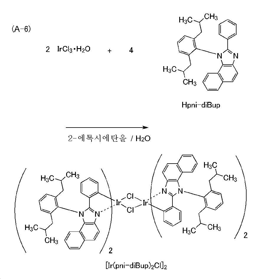
<단계 7; 트리스{2-[1-(2,6-다이아이소뷰틸페닐)-1H-나프토[1,2-d]이미다졸-2-일-κN3]페닐-κC}이리듐(III)(약칭: [Ir(pni-diBup)3])의 합성><
단계 6의 방법으로 합성한 다이-μ-클로로-테트라키스{2-[1-(2,6-다이아이소뷰틸페닐)-1H-나프토[1,2-d]이미다졸-2-일-κN3]페닐-κC}다이이리듐(III)(약칭: [Ir(pni-diBup)2Cl]2) 2.0g(0.92mmol), 다이클로로메테인 150mL를 500mL 3구 플라스크에 넣고, 질소 기류하에서 교반하였다. 이 혼합 용액에 트라이플루오로메테인설폰산 은 0.72g(2.8mmol)과 메탄올 150mL의 혼합 용액을 적하하고, 암소에서 3일 동안 교반하였다. 소정 시간 반응시킨 후, 반응 혼합물을 셀라이트에 통과시켜 여과하였다. 얻어진 여과액을 농축하여, 황색 고체를 2.7g 얻었다. 얻어진 고체 2.7g, 에탄올 50mL, 단계 5의 방법으로 합성한 1-(2,6-다이아이소뷰틸페닐)-2-페닐-1H-나프토[1,2-d]이미다졸(약칭: Hpni-diBup) 1.6g(3.7mmol)을 500mL 가지형 플라스크에 넣고, 질소 기류하에서 20시간 가열 환류하였다. 소정 시간 반응시킨 후, 반응 혼합물을 흡인 여과하여 고체를 얻었다. 얻어진 고체를 다이클로로메테인에 용해시키고, 셀라이트/중성 실리카/셀라이트를 통하여 흡인 여과하였다. 얻어진 여과액을 농축하여, 고체를 얻었다. 얻어진 고체를 실리카 칼럼 크로마토그래피에 의하여 정제하였다. 전개 용매에는 다이클로로메테인:헥세인=1:3을 사용하였다. 얻어진 프랙션을 농축하여 고체를 얻었다. 얻어진 고체를 아세트산에틸/헥세인을 사용하여 재결정하여, 고체를 1.1g, 수율 40%로 얻었다. 합성 스킴을 하기 식(A-7)으로 나타내었다.Di-μ-chloro-tetrakis {2-[1-(2,6-diisobutylphenyl)-1H-naphtho[1,2-d]imidazol-2-yl- synthesized by the method of step 6- κN 3 ]phenyl-κC}diiridium (III) (abbreviation: [Ir(pni-diBup) 2 Cl] 2 ) 2.0 g (0.92 mmol), 150 mL of dichloromethane was added to a 500 mL 3-neck flask, under a nitrogen stream Stirred. To this mixed solution, a mixed solution of 0.72 g (2.8 mmol) of silver trifluoromethanesulfonic acid and 150 mL of methanol was added dropwise, followed by stirring in the dark for 3 days. After reacting for a predetermined time, the reaction mixture was filtered through celite. The obtained filtrate was concentrated to obtain 2.7 g of a yellow solid. 2.7 g of the obtained solid, 50 mL of ethanol, 1-(2,6-diisobutylphenyl)-2-phenyl-1H-naphtho[1,2-d]imidazole (abbreviation: Hpni- diBup) 1.6 g (3.7 mmol) was placed in a 500 mL eggplant flask, and heated to reflux for 20 hours under a flow of nitrogen. After reacting for a predetermined time, the reaction mixture was suction filtered to obtain a solid. The obtained solid was dissolved in dichloromethane, and filtered with suction through celite/neutral silica/celite. The obtained filtrate was concentrated to obtain a solid. The obtained solid was purified by silica column chromatography. Dichloromethane:hexane = 1:3 was used as the developing solvent. The obtained fraction was concentrated to obtain a solid. The obtained solid was recrystallized using ethyl acetate/hexane to obtain a solid in 1.1 g and a yield of 40%. The synthesis scheme is represented by the following formula (A-7).
[화학식 57][Chemical Formula 57]

얻어진 고체 1.1g을 트레인 서블리메이션법에 의하여 승화 정제하였다. 승화 정제는 압력 2.6Pa, 아르곤 유량 10.5mL/min의 조건에서, 얻어진 고체를 340℃에서 41시간 가열하여 수행하였다. 승화 정제 후, 황색 고체를 0.93g, 회수율 88%로 얻었다. 1.1 g of the obtained solid was subjected to sublimation purification by a train sublimation method. Sublimation purification was performed by heating the obtained solid at 340° C. for 41 hours under conditions of a pressure of 2.6 Pa and an argon flow rate of 10.5 mL/min. After sublimation purification, a yellow solid was obtained at 0.93 g and a recovery rate of 88%.
상기에서 얻어진 황색 고체의 프로톤 NMR(1H-NMR) 측정을 수행하였다. 얻어진 값을 이하에 나타낸다. 또한 1H-NMR 차트를 도 12에 나타내었다. 도 12로부터, 본 발명의 일 형태의 유기 금속 착체인 [Ir(pni-diBup)3]이 얻어진 것을 알 수 있었다. The proton NMR (1 H-NMR) measurement of the yellow solid obtained above was performed. The obtained values are shown below. In addition, a 1 H-NMR chart is shown in FIG. 12. From Fig. 12, it was found that [Ir(pni-diBup) 3 ], which is an organometallic complex of one embodiment of the present invention, was obtained.
1H-NMR.δ(CD2Cl2): 0.15(d, 9H), 0.39-0.42(m, 18H), 0.59(d, 9H), 1.27-1.35(m, 3H), 1.78-1.86(m, 3H), 1.93-2.02(m, 6H), 2.33(d, 6H), 6.35-6.40(m, 6H), 6.56-6.61(m, 6H), 7.04-7.07(m, 6H), 7.16(t, 3H), 7.25(d, 3H), 7.30(t, 3H), 7.40(d, 3H), 7.48(d, 3H), 7.63(t, 3H), 7.73(d, 3H). 1 H-NMR.δ(CD 2 Cl 2 ): 0.15(d, 9H), 0.39-0.42(m, 18H), 0.59(d, 9H), 1.27-1.35(m, 3H), 1.78-1.86(m) , 3H), 1.93-2.02(m, 6H), 2.33(d, 6H), 6.35-6.40(m, 6H), 6.56-6.61(m, 6H), 7.04-7.07(m, 6H), 7.16(t , 3H), 7.25 (d, 3H), 7.30 (t, 3H), 7.40 (d, 3H), 7.48 (d, 3H), 7.63 (t, 3H), 7.73 (d, 3H).
이어서, [Ir(pni-diBup)3] 용액의 자외 가시 흡수 스펙트럼(이하, 단순히 '흡수 스펙트럼'이라고 함) 및 발광 스펙트럼을 측정하였다. 흡수 스펙트럼의 측정에는, 자외 가시 분광 광도계(JASCO Corporation 제조 V550형)를 사용하고, [Ir(pni-diBup)3]의 다이클로로메테인 탈산소 용액(0.0089mmol/L)을 석영 셀에 넣고, 실온에서 측정을 수행하였다. 또한, 발광 스펙트럼의 측정과 발광 양자 수율의 측정에는, 절대 PL 양자 수율 측정 장치(Hamamatsu Photonics K.K. 제조 C11347-01)를 사용하고, 글로브 박스(Bright Co., Ltd. 제조 LABstarM13(1250/780))로, 질소 분위기하에서 다이클로로메테인 탈산소 용액(0.0089mmol/L)을 석영 셀에 넣고 밀봉하고, 실온에서 측정을 수행하였다. 얻어진 흡수 스펙트럼 및 발광 스펙트럼의 측정 결과를 도 13에 나타내었다. 가로축은 파장을 나타내고, 세로축은 흡수 강도 및 발광 강도를 나타낸다. 또한, 도 13에 나타내어진 흡수 스펙트럼은 다이클로로메테인 탈산소 용액을 석영 셀에 넣고 측정한 흡수 스펙트럼으로부터 다이클로로메테인만을 석영 셀에 넣고 측정한 흡수 스펙트럼을 뺀 결과를 나타낸 것이다.Subsequently, the ultraviolet and visible absorption spectrum (hereinafter, simply referred to as “absorption spectrum”) and emission spectrum of the [Ir(pni-diBup) 3] solution were measured. For the measurement of the absorption spectrum, an ultraviolet-visible spectrophotometer (V550 type manufactured by JASCO Corporation) was used, and a dichloromethane deoxygenation solution (0.0089 mmol/L) of [Ir (pni-diBup) 3] was put in a quartz cell, Measurements were carried out at room temperature. In addition, for the measurement of the emission spectrum and the measurement of the emission quantum yield, an absolute PL quantum yield measurement device (C11347-01 manufactured by Hamamatsu Photonics KK) was used, and a glove box (LABstarM13 (1250/780) manufactured by Bright Co., Ltd.) was used. In a nitrogen atmosphere, a dichloromethane deoxygenation solution (0.0089 mmol/L) was put into a quartz cell, sealed, and measurement was performed at room temperature. Fig. 13 shows the measurement results of the absorption spectrum and emission spectrum obtained. The horizontal axis represents wavelength, and the vertical axis represents absorption intensity and light emission intensity. In addition, the absorption spectrum shown in FIG. 13 shows the result of subtracting the absorption spectrum measured by putting only dichloromethane in the quartz cell from the absorption spectrum measured by putting the dichloromethane deoxygenation solution in the quartz cell.
도 13에 나타낸 바와 같이, 이리듐 착체 [Ir(pni-diBup)3]은 500, 536nm에 발광 피크를 가지고, 다이클로로메테인 탈산소 용액으로부터는 녹색의 발광이 관측되었다.As shown in Fig. 13, the iridium complex [Ir(pni-diBup) 3 ] had emission peaks at 500 and 536 nm, and green light emission was observed from the dichloromethane deoxygenation solution.
또한, 다이클로로메테인 탈산소 용액에서의 여기 파장 450nm에서의 발광 양자 수율을 측정한 결과, 98%로 매우 높은 것을 알 수 있었다. In addition, as a result of measuring the light emission quantum yield at an excitation wavelength of 450 nm in the dichloromethane deoxygenation solution, it was found that it was very high as 98%.
(실시예 2)(Example 2)
본 실시예에서는, 실시형태 1에서 구조식(101)으로 나타낸 본 발명의 일 형태의 유기 금속 착체인, 비스{2-[1-(2,6-다이아이소뷰틸페닐)-1H-나프토[1,2-d]이미다졸-2-일-κN3]페닐-κC}[2-(4-메틸-5-페닐-2-피리딜-κN2)페닐-κC]이리듐(III)(약칭: [Ir(pni-diBup)2(mdppy)])의 합성 방법에 대하여 설명한다.In this example, bis(2-[1-(2,6-diisobutylphenyl)-1H-naphtho[1), which is an organometallic complex of one embodiment of the present invention represented by structural formula (101) in
<단계 1; 비스{2-[1-(2,6-다이아이소뷰틸페닐)-1H-나프토[1,2-d]이미다졸-2-일-κN3]페닐-κC}[2-(4-메틸-5-페닐-2-피리딜-κN2)페닐-κC]이리듐(III)(약칭: [Ir(pni-diBup)2(mdppy)])의 합성><
다이-μ-클로로-테트라키스[2-(4-메틸-5-페닐-2-피리딘일-κN)페닐-κC]다이이리듐(III)(약칭: [Ir(mdppy)2Cl]2) 1.3g(0.9mmol), 다이클로로메테인 180mL를, 500mL 3구 플라스크에 넣고, 질소 기류하에서 교반하였다. 이 혼합 용액에 트라이플루오로메테인설폰산 은 0.7g(2.7mmol)과 메탄올 35mL의 혼합 용액을 적하하고, 암소에서 18시간 교반하였다. 소정 시간 반응시킨 후, 반응 혼합물을 셀라이트에 통과시켜 여과하였다. 얻어진 여과액을 농축하여, 황색 고체를 1.9g 얻었다. 얻어진 황색 고체 1.9g, 메탄올 30mL, 에탄올 30mL, Hpni-diBup 1.6g(3.6mmol)을 300mL 가지형 플라스크에 넣고, 질소 기류하에서 23시간 가열 환류하였다. 소정 시간 반응시킨 후, 반응 혼합물을 흡인 여과하여, 불용물(不溶物)을 제거한 후, 여과액을 농축하여 고체를 얻었다. 얻어진 고체에 1-뷰탄올 60mL를 첨가하여, 질소 기류하에서 22시간 가열 환류하였다. 소정 시간 반응시킨 후, 반응 혼합물을 흡인 여과하여 고체를 얻었다. 얻어진 고체를 실리카 칼럼 크로마토그래피에 의하여 정제하였다. 전개 용매에는 헥세인:다이클로로메테인=3:1의 혼합 용매를 사용하였다. 얻어진 프랙션을 농축하여 고체를 얻었다. 얻어진 고체를 아세트산에틸/헥세인을 사용하여 재결정하여, 목적물인 황색 고체를 0.20g, 수율 9%로 얻었다. 합성 스킴을 하기 식(B-1)으로 나타내었다.Di-μ-chloro-tetrakis[2-(4-methyl-5-phenyl-2-pyridinyl-κN)phenyl-κC]diiridium(III) (abbreviation: [Ir(mdppy) 2 Cl] 2 ) 1.3 g (0.9 mmol) and 180 mL of dichloromethane were placed in a 500 mL three-necked flask, and stirred under a nitrogen stream. To this mixed solution, a mixed solution of 0.7 g (2.7 mmol) of silver trifluoromethanesulfonic acid and 35 mL of methanol was added dropwise, followed by stirring in the dark for 18 hours. After reacting for a predetermined time, the reaction mixture was filtered through celite. The obtained filtrate was concentrated to obtain 1.9 g of a yellow solid. 1.9 g of the obtained yellow solid, 30 mL of methanol, 30 mL of ethanol, and 1.6 g (3.6 mmol) of Hpni-diBup were placed in a 300 mL eggplant-shaped flask, and heated to reflux for 23 hours under a nitrogen stream. After reacting for a predetermined time, the reaction mixture was suction filtered to remove insoluble matters, and the filtrate was concentrated to obtain a solid. 60 mL of 1-butanol was added to the obtained solid, and it was heated and refluxed for 22 hours under a nitrogen stream. After reacting for a predetermined time, the reaction mixture was suction filtered to obtain a solid. The obtained solid was purified by silica column chromatography. A mixed solvent of hexane:dichloromethane=3:1 was used as the developing solvent. The obtained fraction was concentrated to obtain a solid. The obtained solid was recrystallized using ethyl acetate/hexane to obtain a target yellow solid in 0.20 g and a yield of 9%. The synthesis scheme is represented by the following formula (B-1).
[화학식 58][Chemical Formula 58]

얻어진 고체 0.19g을 트레인 서블리메이션법에 의하여 승화 정제하였다. 승화 정제는 압력 2.5Pa, 아르곤 유량 10.3mL/min의 조건에서, 얻어진 고체를 320℃에서 18시간 가열하여 수행하였다. 승화 정제 후, 황색 고체를 0.14g, 회수율 72%로 얻었다. 0.19 g of the obtained solid was subjected to sublimation purification by a train sublimation method. Sublimation purification was carried out by heating the obtained solid at 320° C. for 18 hours under conditions of a pressure of 2.5 Pa and an argon flow rate of 10.3 mL/min. After sublimation purification, a yellow solid was obtained at 0.14 g and a recovery rate of 72%.
상기에서 얻어진 황색 고체의 1H-NMR 측정을 수행하였다. 얻어진 값을 이하에 나타낸다. 또한 1H-NMR 차트를 도 14에 나타내었다. 도 14로부터, 본 발명의 일 형태의 유기 금속 착체인 [Ir(pni-diBup)2(mdppy)]가 얻어진 것을 알 수 있었다. 1 H-NMR measurement of the yellow solid obtained above was performed. The obtained values are shown below. In addition, a 1 H-NMR chart is shown in FIG. 14. From Fig. 14, it was found that [Ir(pni-diBup) 2 (mdppy)], which is an organometallic complex of one embodiment of the present invention, was obtained.
1H-NMR.δ(CD2Cl2): 0.09-0.15(m, 9H), 0.29-0.34(m, 9H), 0.40(t, 1H), 0.45(d, 3H), 0.51(d, 3H), 1.18-1.24(m, 1H), 1.34-1.49(m, 1H), 1.70-1.78(m, 1H), 1.88-2.09(m, 6H), 2.17-2.25(m, 2H), 2.51(s, 3H), 6.30-6.40(m, 3H), 6.48(t, 1H), 6.61-6.52(m, 3H), 6.64-6.69(m, 2H), 6.74-6.79(m, 2H), 6.83(t, 1H), 6.93-7.01(m, 3H), 7.08(t, 1H), 7.13-7.25(m, 8H), 7.34-7.51(m, 6H), 7.57-7.73(m, 4H), 7.87(d, 1H), 7.94(s, 1H), 8.31(s, 1H). 1 H-NMR.δ(CD 2 Cl 2 ): 0.09-0.15(m, 9H), 0.29-0.34(m, 9H), 0.40(t, 1H), 0.45(d, 3H), 0.51(d, 3H) ), 1.18-1.24(m, 1H), 1.34-1.49(m, 1H), 1.70-1.78(m, 1H), 1.88-2.09(m, 6H), 2.17-2.25(m, 2H), 2.51(s , 3H), 6.30-6.40(m, 3H), 6.48(t, 1H), 6.61-6.52(m, 3H), 6.64-6.69(m, 2H), 6.74-6.79(m, 2H), 6.83(t , 1H), 6.93-7.01 (m, 3H), 7.08 (t, 1H), 7.13-7.25 (m, 8H), 7.34-7.51 (m, 6H), 7.57-7.73 (m, 4H), 7.87 (d , 1H), 7.94 (s, 1H), 8.31 (s, 1H).
이어서, [Ir(pni-diBup)2(mdppy)]의 다이클로로메테인 탈산소 용액(0.0073mmol/L)의 흡수 스펙트럼, 발광 스펙트럼, 및 발광 양자 수율을 측정하였다. 측정은 실시예 1과 마찬가지로 수행하였다. 흡수 스펙트럼과 발광 스펙트럼의 측정 결과를 도 15에 나타내었다.Then, the absorption spectrum, emission spectrum, and emission quantum yield of the dichloromethane deoxygenation solution (0.0073 mmol/L) of [Ir(pni-diBup) 2 (mdppy)] were measured. Measurement was carried out in the same manner as in Example 1. The measurement results of the absorption spectrum and the emission spectrum are shown in FIG. 15.
도 15에 나타낸 바와 같이, 이리듐 착체 [Ir(pni-diBup)2(mdppy)]는 530nm에 발광 피크를 가지고, 다이클로로메테인 탈산소 용액으로부터는 녹색의 발광이 관측되었다.As shown in Fig. 15, the iridium complex [Ir(pni-diBup) 2 (mdppy)] had an emission peak at 530 nm, and green light emission was observed from the dichloromethane deoxygenation solution.
또한, 다이클로로메테인 탈산소 용액(0.0073mmol/L)으로 여기 파장 450nm에서의 발광 양자 수율을 측정한 결과, 98%로 매우 높은 것을 알 수 있었다. In addition, as a result of measuring the emission quantum yield at an excitation wavelength of 450 nm with a dichloromethane deoxygenation solution (0.0073 mmol/L), it was found that it was very high as 98%.
(실시예 3)(Example 3)
본 실시예에서는, 실시형태 1에서 구조식(102)으로 나타낸 본 발명의 일 형태의 유기 금속 착체인 트리스{2-[1-(4-사이아노-2-아이소뷰틸페닐)-1H-나프토[1,2-d]이미다졸-2-일-κN3]페닐-κC}이리듐(III)(약칭: [Ir(pni-iBuCNp)3])의 합성 방법에 대하여 설명한다.In this example, tris {2-[1-(4-cyano-2-isobutylphenyl)-1H-naphtho[ A method for synthesizing 1,2-d]imidazol-2-yl-κN 3 ]phenyl-κC}iridium (III) (abbreviation: [Ir(pni-iBuCNp) 3 ]) will be described.
<단계 1; 4-아미노-3-아이소뷰틸벤조나이트릴의 합성><
4-아미노-3-클로로벤조나이트릴 75g(492mmol), 아이소뷰틸보론산 90g(886mmol), 인산 삼포타슘 188g(886mmol), 2-다이사이클로헥실포스피노-2',6'-다이메톡시바이페닐(S-phos) 4.0g(9.8mmol), 톨루엔 2400mL를 5000mL 3구 플라스크에 넣고, 플라스크 내를 질소 치환하고, 플라스크 내를 감압하면서 교반하여 이 혼합물을 탈기하였다. 탈기 후, 트리스(다이벤질리덴아세톤)다이팔라듐(0) 4.5g(4.9mmol)을 첨가하고 질소 기류하, 120℃에서 20시간 교반하였다. 소정 시간 경과 후, 얻어진 반응 용액을 흡인 여과하였다. 얻어진 여과액을 톨루엔을 사용한 추출에 의하여 정제하였다. 그 후, 실리카 칼럼 크로마토그래피에 의하여 정제하였다. 전개 용매에는 톨루엔을 사용하였다. 얻어진 프랙션을 농축하여, 목적물인 갈색 유상 물질을 59g, 수율 69%로 얻었다. 단계 1의 합성 스킴을 하기 식(C-1)으로 나타내었다.
4-amino-3-chlorobenzonitrile 75g (492mmol), isobutylboronic acid 90g (886mmol), tripotassium phosphate 188g (886mmol), 2-dicyclohexylphosphino-2',6'-dimethoxybi Phenyl (S-phos) 4.0 g (9.8 mmol) and toluene 2400 mL were put into a 5000 mL three-neck flask, the inside of the flask was replaced with nitrogen, and the flask was stirred under reduced pressure to degas the mixture. After degassing, 4.5 g (4.9 mmol) of tris(dibenzylideneacetone)dipalladium (0) was added, followed by stirring at 120°C for 20 hours under a nitrogen stream. After the lapse of a predetermined time, the obtained reaction solution was suction-filtered. The obtained filtrate was purified by extraction with toluene. Then, it was purified by silica column chromatography. Toluene was used as the developing solvent. The obtained fraction was concentrated to obtain a target object, a brown oily substance in 59 g and a yield of 69%. The synthesis scheme of
[화학식 59][Chemical Formula 59]

<단계 2; 3-아이소뷰틸-4-[N-(2-나이트로나프틸)아미노]벤조나이트릴의 합성><
단계 1에서 합성한 4-아미노-3-아이소뷰틸벤조나이트릴 30g(170mmol), 2-나이트로나프탈렌-1-트라이플루오로메테인설포네이트 45g(141mmol), 탄산 세슘 78g(240mmol), 톨루엔 750mL를 2000mL 3구 플라스크에 넣고, 플라스크 내를 질소 치환하고, 플라스크 내를 감압하면서 교반하여 이 혼합물을 탈기하였다. 탈기 후, 2-다이사이클로헥실포스피노-2',6'-다이메톡시바이페닐(S-phos) 4.6g(11mmol), 트리스(다이벤질리덴아세톤)다이팔라듐(0) 2.6g(2.8mmol)을 첨가하고 질소 기류하, 130℃에서 24시간 교반하였다. 소정 시간 경과 후, 얻어진 반응 혼합물을 톨루엔을 사용한 추출에 의하여 정제하였다. 그 후, 실리카 칼럼 크로마토그래피에 의하여 정제하였다. 전개 용매에는 헥세인:아세트산에틸=10:1을 사용하였다. 얻어진 프랙션을 농축하여, 목적물의 황색 유상 물질을 40g, 수율 82%로 얻었다. 단계 2의 합성 스킴을 하기 식(C-2)으로 나타내었다.
4-amino-3-isobutylbenzonitrile 30g (170mmol) synthesized in
[화학식 60][Chemical Formula 60]

<단계 3; 3-아이소뷰틸-4-[N-(1,2-나프탈렌다이아민)]벤조나이트릴의 합성><
단계 2에서 합성한 3-아이소뷰틸-4-[N-(2-나이트로나프틸)아미노]벤조나이트릴 40g(115mmol), 물 21mL(1.2mol), 에탄올 1350mL를 3000mL 3구 플라스크에 넣고 교반하였다. 이 혼합물에 염화 주석(II) 109g(0.58mol)을 첨가하고 질소 기류하, 80℃에서 6시간 교반하였다. 소정 시간 경과 후, 얻어진 반응 혼합물을 2M 수산화 소듐 수용액 500mL에 따르고, 2시간 실온에서 교반하였다. 석출한 침전물을 흡인 여과하고, 클로로폼으로 세정하여 여과액을 얻었다. 얻어진 여과액을 클로로폼을 사용한 추출에 의하여 정제하였다. 그 후, 얻어진 고체에 헥세인을 첨가하고, 흡인 여과하여 백색 고체를 32g, 수율 88%로 얻었다. 단계 3의 합성 스킴을 하기 식(C-3)으로 나타내었다.
3-isobutyl-4-[N-(2-nitronaphthyl)amino]benzonitrile 40 g (115 mmol) synthesized in
[화학식 61][Chemical Formula 61]

<단계 4; 1-(4-사이아노-2-아이소뷰틸페닐)-2-페닐-1H-나프토[1,2-d]이미다졸(약칭: Hpni-iBuCNp)의 합성><
단계 3에서 합성한 3-아이소뷰틸-4-[N-(1,2-나프탈렌다이아민)]벤조나이트릴 32g(101mmol), 아세토나이트릴 400mL, 벤즈알데하이드 11g(101mmol)을 1000mL 3구 플라스크에 넣고, 100℃에서 6시간 교반하였다. 이 혼합물에 염화철(III) 0.16g(1.0mmol)을 첨가하고 100℃에서 16시간 교반하였다. 소정 시간 경과 후, 얻어진 반응 혼합물을 아세트산에틸을 사용하여 추출하였다. 그 후, 얻어진 고체를 실리카 칼럼 크로마토그래피에 의하여 정제하였다. 전개 용매에는 우선 톨루엔을 사용하고, 이어서 톨루엔:아세트산에틸=18:1의 혼합 용매를 사용하였다. 얻어진 프랙션을 농축하여 고체를 얻었다. 얻어진 고체에 아세트산에틸을 첨가하고, 흡인 여과하여 목적물인 백색 고체를 14g, 수율 34%로 얻었다. 단계 4의 합성 스킴을 하기 식(C-4)으로 나타내었다.
3-isobutyl-4-[N-(1,2-naphthalenediamine)]benzonitrile 32 g (101 mmol) synthesized in
[화학식 62][Formula 62]

<단계 5; 트리스{2-[1-(4-사이아노-2-아이소뷰틸페닐)-1H-나프토[1,2-d]이미다졸-2-일-κN3]페닐-κC}이리듐(III)(약칭: [Ir(pni-iBuCNp)3])의 합성><
단계 4의 방법으로 합성한 1-(4-사이아노-2-아이소뷰틸페닐)-2-페닐-1H-나프토[1,2-d]이미다졸 3.8g(9.5mmol), 트리스(아세틸아세토네이토)이리듐(III) 0.93g(1.9mmol)을 3방 콕이 제공된 반응 용기에 넣고, 250℃에서 40시간 가열하였다. 얻어진 반응 혼합물에 다이클로로메테인을 첨가하여, 불용물을 제거하였다. 얻어진 여과액을 농축하여 고체를 얻었다. 얻어진 고체를 실리카 칼럼 크로마토그래피에 의하여 정제하였다. 전개 용매에는 다이클로로메테인을 사용하였다. 얻어진 프랙션을 농축하여 고체를 얻었다. 얻어진 고체를 아세트산에틸/헥세인을 사용하여 재결정하여, 황색 고체를 0.3g, 수율 10%로 얻었다. 본 합성 스킴을 하기 식(C-5)으로 나타내었다.
1-(4-cyano-2-isobutylphenyl)-2-phenyl-1H-naphtho[1,2-d]imidazole 3.8g (9.5mmol) synthesized by the method of
[화학식 63][Chemical Formula 63]

상기에서 얻어진 황색 고체의 질량(MS)을 측정하였다. 얻어진 화합물의 ESI-MS 측정 결과를 이하에 나타낸다. ESI-MS[M+H+]=1394.51(Exact Mass=1393.51). 이로부터, 상술한 구조식(102)으로 나타내어지는 본 발명의 유기 금속 착체의 일 형태인 [Ir(pni-iBuCNp)3])이 얻어진 것을 알 수 있었다.The mass (MS) of the yellow solid obtained above was measured. The ESI-MS measurement results of the obtained compound are shown below. ESI-MS[M+H + ]=1394.51 (Exact Mass=1393.51). From this, it was found that [Ir(pni-iBuCNp) 3 ]), which is a form of the organometallic complex of the present invention represented by the above-described structural formula (102), was obtained.
이어서, 상기에서 얻어진 [Ir(pni-iBuCNp)3]의 다이클로로메테인 탈산소 용액(0.013mmol/L)의 흡수 스펙트럼 및 발광 스펙트럼을 측정하였다. 측정은 실시예 1과 마찬가지로 수행하였다. 흡수 스펙트럼 및 발광 스펙트럼을 도 16에 나타내었다.Next, the absorption spectrum and emission spectrum of the dichloromethane deoxygenation solution (0.013 mmol/L) of [Ir(pni-iBuCNp) 3] obtained above were measured. Measurement was carried out in the same manner as in Example 1. The absorption spectrum and emission spectrum are shown in FIG. 16.
도 16에 나타낸 바와 같이, 이리듐 착체 [Ir(pni-iBuCNp)3]은 509, 544nm에 발광 피크를 가지고, 다이클로로메테인 탈산소 용액으로부터는 녹색의 발광이 관측되었다.As shown in Fig. 16, the iridium complex [Ir(pni-iBuCNp) 3 ] had emission peaks at 509 and 544 nm, and green light emission was observed from the dichloromethane deoxygenation solution.
(실시예 4)(Example 4)
본 실시예에서는, 실시형태 1에서 구조식(103)으로 나타낸 본 발명의 일 형태의 유기 금속 착체인 트리스{2-[1-(4-사이아노-2,6-다이아이소뷰틸페닐)-1H-나프토[1,2-d]이미다졸-2-일-κN3]페닐-κC}이리듐(III)(약칭: [Ir(pni-diBuCNp)3])의 합성 방법에 대하여 설명한다.In this example, tris (2-[1-(4-cyano-2,6-diisobutylphenyl)-1H-, which is an organometallic complex of one embodiment of the present invention represented by the structural formula (103) in Embodiment 1) A method for synthesizing naphtho[1,2-d]imidazol-2-yl-κN 3 ]phenyl-κC}iridium(III) (abbreviation: [Ir(pni-diBuCNp) 3 ]) will be described.
<단계 1; 4-아미노-3,5-다이아이소뷰틸벤조나이트릴의 합성><
4-아미노-3,5-다이아이소뷰틸벤조나이트릴 58g(310mmol), 아이소뷰틸보론산 117g(1145mmol), 인산 삼포타슘 243g(1145mmol), 2-다이사이클로헥실포스피노-2',6'-다이메톡시바이페닐(S-phos) 6.4g(15.5mmol), 톨루엔 1500ml를 3000mL 3구 반응 용기에 넣고, 플라스크 내를 질소 치환하고, 플라스크 내를 감압하면서 교반하여 이 혼합물을 탈기하였다. 탈기 후, 트리스(다이벤질리덴아세톤)다이팔라듐(0) 5.7g(6.2mmol)을 첨가하고 질소 기류하, 130℃에서 12시간 교반하였다. 얻어진 반응 용액에 톨루엔을 첨가하고, 셀라이트를 통하여 흡인 여과하였다. 얻어진 여과액을 톨루엔을 사용한 추출에 의하여 정제하였다. 그 후, 실리카 칼럼 크로마토그래피에 의하여 정제하였다. 전개 용매에는 톨루엔을 사용하였다. 얻어진 프랙션을 농축하여, 목적물의 황색 유상 물질을 69g, 수율 96%로 얻었다. 단계 1의 합성 스킴을 하기 식(D-1)으로 나타내었다.
4-amino-3,5-diisobutylbenzonitrile 58g (310mmol), isobutylboronic acid 117g (1145mmol), tripotassium phosphate 243g (1145mmol), 2-dicyclohexylphosphino-2',6'- Dimethoxybiphenyl (S-phos) 6.4 g (15.5 mmol) and toluene 1500 ml were placed in a 3000 mL three-neck reaction vessel, the inside of the flask was replaced with nitrogen, and the inside of the flask was stirred under reduced pressure, and the mixture was degassed. After degassing, 5.7 g (6.2 mmol) of tris(dibenzylideneacetone)dipalladium (0) was added, followed by stirring at 130°C for 12 hours under a nitrogen stream. Toluene was added to the obtained reaction solution, and suction filtration was carried out through Celite. The obtained filtrate was purified by extraction with toluene. Then, it was purified by silica column chromatography. Toluene was used as the developing solvent. The obtained fraction was concentrated to obtain 69 g of a yellow oily substance of the target substance in a yield of 96%. The synthesis scheme of
[화학식 64][Formula 64]

<단계 2; 3,5-다이아이소뷰틸-4-[N-(2-나이트로나프틸)아미노]벤조나이트릴의 합성><
단계 1에서 합성한 4-아미노-3,5-다이아이소뷰틸벤조나이트릴 28g(121mmol), 2-나이트로나프탈렌-1-트라이플루오로메테인설포네이트 39g(121mmol), 탄산 세슘 67g(205mmol), 톨루엔 750mL를 2000mL 3구 플라스크에 넣고, 플라스크 내를 질소 치환하고, 플라스크 내를 감압하면서 교반하여 이 혼합물을 탈기하였다. 탈기 후, 2-다이사이클로헥실포스피노-2',6'-다이메톡시바이페닐(S-phos) 4.0g(9.7mmol), 트리스(다이벤질리덴아세톤)다이팔라듐(0) 2.2g(2.4mmol)을 첨가하고 질소 기류하, 130℃에서 40시간 교반하였다. 소정 시간 경과 후, 얻어진 반응 혼합물을 톨루엔을 사용한 추출에 의하여 정제하였다. 그 후, 실리카 칼럼 크로마토그래피에 의하여 정제하였다. 전개 용매에는 헥세인:아세트산에틸=10:1을 사용하였다. 얻어진 프랙션을 농축하여, 목적물인 주황색 고체를 4.5g, 수율 9%로 얻은 단계 2의 합성 스킴을 하기 식(D-2)으로 나타내었다.
4-amino-3,5-diisobutylbenzonitrile 28g (121mmol) synthesized in
[화학식 65][Formula 65]

<단계 3; 3,5-다이아이소뷰틸-4-[N-(1,2-나프탈렌다이아민)]벤조나이트릴의 합성><
단계 2에서 합성한 3,5-다이아이소뷰틸-4-[N-(2-나이트로나프틸)아미노]벤조나이트릴 4.5g(11mmol), 물 2mL(110mmol), 에탄올 130mL를 500mL 3구 플라스크에 넣고 교반하였다. 이 혼합물에 염화 주석(II) 10.4g(55mmol)을 첨가하고, 질소 기류하, 80℃에서 7.5시간 교반하였다. 소정 시간 경과 후, 얻어진 반응 혼합물을 2M 수산화 소듐 수용액 100mL에 따르고, 2시간 실온에서 교반하였다. 석출한 침전물을 흡인 여과하고, 클로로폼으로 세정하여 여과액을 얻었다. 얻어진 여과액을 클로로폼을 사용하여 추출하였다. 그 후, 얻어진 추출 용액을 농축하여, 목적물인 흑색 유상 물질을 4.1g, 수율 99%로 얻었다. 단계 3의 합성 스킴을 하기 식(D-3)으로 나타내었다.
3,5-diisobutyl-4-[N-(2-nitronaphthyl)amino]benzonitrile 4.5 g (11 mmol) synthesized in
[화학식 66][Formula 66]
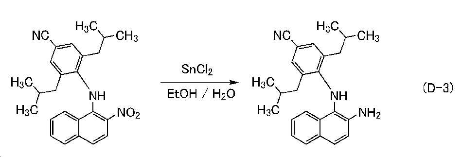
<단계 4; 1-(4-사이아노-2,6-다이아이소뷰틸페닐)-2-페닐-1H-나프토[1,2-d]이미다졸(약칭: Hpni-diBuCNp)의 합성><
단계 3에서 합성한 3,5-다이아이소뷰틸-4-[N-(1,2-나프탈렌다이아민)]벤조나이트릴 4.2g(11mmol), 아세토나이트릴 50mL, 벤즈알데하이드 1.2g(11mmol)을 500mL 3구 플라스크에 넣고, 100℃에서 8시간 교반하였다. 이 혼합물에 염화철(III) 18mg(0.11mmol)을 첨가하고, 100℃에서 29시간 교반하였다. 소정 시간 경과 후, 얻어진 반응 혼합물을 아세트산에틸을 사용한 추출에 의하여 정제하였다. 그 후, 얻어진 고체를 실리카 칼럼 크로마토그래피에 의하여 정제하였다. 전개 용매에는 우선 톨루엔을 사용하고, 이어서 톨루엔:아세트산에틸=20:1의 혼합 용매를 사용하였다. 얻어진 프랙션을 농축하여, 목적물인 흑색 유상 물질을 2.9g, 수율 58%로 얻은 단계 4의 합성 스킴을 하기 식(D-4)으로 나타내었다.
3,5-diisobutyl-4-[N-(1,2-naphthalenediamine)]benzonitrile 4.2 g (11 mmol) synthesized in
[화학식 67][Chemical Formula 67]

<단계 5; 트리스{2-[1-(4-사이아노-2,6-다이아이소뷰틸페닐)-1H-나프토[1,2-d]이미다졸-2-일-κN3]페닐-κC}이리듐(III)(약칭: [Ir(pni-diBuCNp)3])의 합성><
단계 1 내지 4의 방법으로 합성한 1-(4-사이아노-2,6-다이아이소뷰틸페닐)-2-페닐-1H-나프토[1,2-d]이미다졸 2.9g(6.3mmol), 트리스(아세틸아세토네이토)이리듐(III) 0.62g(1.3mmol)을 3방 콕이 제공된 반응 용기에 넣고, 250℃에서 56시간 가열하였다. 얻어진 반응 혼합물에 톨루엔을 첨가하여 여과함으로써, 불용물을 제거하였다. 얻어진 여과액을 농축하여 고체를 얻었다. 얻어진 고체를 실리카 칼럼 크로마토그래피에 의하여 정제하였다. 전개 용매에는 톨루엔을 사용하였다. 얻어진 프랙션을 농축하여 고체를 얻었다. 얻어진 고체를 아세트산에틸/헥세인을 사용하여 재결정하여, 황색 고체를 0.33g, 수율 16%로 얻었다. 합성 스킴을 하기 식 (D-5)에 나타낸다.
1-(4-cyano-2,6-diisobutylphenyl)-2-phenyl-1H-naphtho[1,2-d]imidazole 2.9 g (6.3 mmol) synthesized by the method of
[화학식 68][Chemical Formula 68]

얻어진 고체 0.32g을 트레인 서블리메이션법에 의하여 승화 정제하였다. 승화 정제는 압력 2.5Pa, 아르곤 유량 10.4mL/min의 조건에서, 345℃에서 17시간 가열하여 수행하였다. 승화 정제 후, 0.10g, 회수율 31%로 얻었다. 0.32 g of the obtained solid was subjected to sublimation purification by a train sublimation method. Sublimation purification was carried out by heating at 345° C. for 17 hours under conditions of a pressure of 2.5 Pa and an argon flow rate of 10.4 mL/min. After sublimation purification, it was obtained at 0.10 g and a recovery rate of 31%.
상기에서 얻어진 황색 고체의 1H-NMR를 측정하였다. 얻어진 값을 이하에 나타낸다. 또한 1H-NMR 차트를 도 17에 나타내었다. 도 17로부터, 본 발명의 일 형태의 유기 금속 착체인 [Ir(pni-diBuCNp)3]이 얻어진 것을 알 수 있었다. 1 H-NMR of the yellow solid obtained above was measured. The obtained values are shown below. In addition, a 1 H-NMR chart is shown in FIG. 17. From Fig. 17, it was found that [Ir(pni-diBuCNp) 3 ], which is an organometallic complex of one embodiment of the present invention, was obtained.
1H-NMR.δ(ppm from CH2Cl2), (CD2Cl2): -0.38(d, 3H), -0.13--0.06(m, 9H), 0.35(d, 3H), 0.41-0.45(m, 6H), 0.54-0.57(m, 6H), 0.62-0.65(m, 6H), 0.70(d, 3H), 1.14-1.23(m, 1H), 1.27-1.35(m, 1H), 1.40-1.49(m, 1H), 1.50-1.57(m, 1H), 1.60-1.66(m, 2H), 1.71-1.90(m, 4H), 2.06-2.15(m, 2H), 2.22-2.31(m, 4H), 2.33-2.42(t, 2H), 6.32-6.39(m, 3H), 6.53-6.85(m, 12H), 6.96(t, 2H), 7.06(d, 1H), 7.10-7.37(m, 9H), 7.66-7.83(m, 9H). 1 H-NMR.δ(ppm from CH 2 Cl 2 ), (CD 2 Cl 2 ): -0.38(d, 3H), -0.13--0.06(m, 9H), 0.35(d, 3H), 0.41- 0.45(m, 6H), 0.54-0.57(m, 6H), 0.62-0.65(m, 6H), 0.70(d, 3H), 1.14-1.23(m, 1H), 1.27-1.35(m, 1H), 1.40-1.49 (m, 1H), 1.50-1.57 (m, 1H), 1.60-1.66 (m, 2H), 1.71-1.90 (m, 4H), 2.06-2.15 (m, 2H), 2.22-2.31 (m , 4H), 2.33-2.42(t, 2H), 6.32-6.39(m, 3H), 6.53-6.85(m, 12H), 6.96(t, 2H), 7.06(d, 1H), 7.10-7.37(m) , 9H), 7.66-7.83 (m, 9H).
이어서, [Ir(pni-diBuCNp)3]의 다이클로로메테인 탈산소 용액(0.0084mmol/L)의 흡수 스펙트럼, 발광 스펙트럼, 및 발광 양자 수율을 측정하였다. 흡수 스펙트럼 및 발광 스펙트럼의 측정 결과를 도 18에 나타내었다.Then, the absorption spectrum, emission spectrum, and emission quantum yield of the dichloromethane deoxygenation solution (0.0084 mmol/L) of [Ir(pni-diBuCNp) 3] were measured. The measurement results of the absorption spectrum and the emission spectrum are shown in FIG. 18.
도 18에 나타낸 바와 같이, 이리듐 착체 [Ir(pni-diBuCNp)3]은 510, 547nm에 발광 피크를 가지고, 다이클로로메테인 탈산소 용액으로부터는 녹색의 발광이 관측되었다.As shown in Fig. 18, the iridium complex [Ir(pni-diBuCNp) 3 ] had emission peaks at 510 and 547 nm, and green light emission was observed from the dichloromethane deoxygenation solution.
또한, 다이클로로메테인 탈산소 용액(0.0084mmol/L)에서 여기 파장 450nm일 때의 발광 양자 수율을 측정한 결과, 91%로 매우 높은 것을 알 수 있었다. In addition, as a result of measuring the emission quantum yield at an excitation wavelength of 450 nm in a dichloromethane deoxygenation solution (0.0084 mmol/L), it was found to be very high as 91%.
(실시예 5)(Example 5)
상술한 바와 같이 합성한 [Ir(pni-diBup)3], [Ir(pni-diBup)2(mdppy)], [Ir(pni-diBuCNp)3]의 발광 양자 수율 측정을 수행하였다. 또한, 비교 물질인 (OC-6-22)-트리스{2-[1-(2,6-다이아이소뷰틸페닐)-1H-벤즈이미다졸-2-일-κN3]페닐-κC}이리듐(III)(약칭: fac-[Ir(pbi-diBup)3]의 발광 양자 수율도 측정하였다. 측정은 실시예 1에 기재된 방법과 마찬가지로 수행하였다. 그 결과를 표 1에 나타낸다.The emission quantum yield measurements of [Ir(pni-diBup) 3 ], [Ir(pni-diBup) 2 (mdppy)], and [Ir(pni-diBuCNp) 3] synthesized as described above were performed. In addition, the comparative substance (OC-6-22)-tris {2-[1-(2,6-diisobutylphenyl)-1H-benzimidazol-2-yl-κN 3 ]phenyl-κC}iridium ( III) (abbreviation: fac-[Ir(pbi-diBup) 3 ] was also measured for the luminescence quantum yield. The measurement was carried out in the same manner as in Example 1. Table 1 shows the results.

본 발명의 일 형태의 유기 금속 착체인 [Ir(pni-diBup)3]과 fac-[Ir(pbi-diBup)3]의 구조의 차이는 벤즈이미다졸 골격의 g위치에 축환된 벤젠 고리를 가지는지 여부이다. 표 1에 나타낸 바와 같이, 본 발명의 일 형태의 유기 금속 착체가 더 양호한 발광 양자 수율을 나타내었다. 또한, 1H-나프토[1,2-d]이미다졸 골격을 리간드에 가지는 유기 금속 착체는 발광 양자 수율이 90%를 넘는 매우 높은 발광 양자 수율을 나타낸다는 것을 알 수 있었다. The difference in structure between [Ir(pni-diBup) 3 ] and fac-[Ir(pbi-diBup) 3 ], which is an organometallic complex of one embodiment of the present invention, has a benzene ring condensed at the g position of the benzimidazole skeleton. Whether or not. As shown in Table 1, the organometallic complex of one embodiment of the present invention exhibited a better light emission quantum yield. In addition, it was found that the organometallic complex having a 1H-naphtho[1,2-d]imidazole skeleton in the ligand exhibits a very high light emission quantum yield exceeding 90% of the light emission quantum yield.
(실시예 6)(Example 6)
본 실시예에서는 본 발명의 일 형태에 따른 유기 화합물을 포함하는 발광 소자 및 비교 발광 소자의 제작예와 상기 발광 소자의 특성에 대하여 설명한다. 본 실시예에서 제작된 발광 소자의 적층 구조를 도 1의 (A)에 도시하였다. 또한, 소자 구조의 자세한 사항을 표 2에 나타낸다. 또한 본 실시예에서 사용하는 유기 화합물을 이하에 나타내었다. 또한 다른 유기 화합물에 대해서는 다른 실시형태 또는 실시예를 참조하면 좋다. In this embodiment, examples of fabrication of a light-emitting device including an organic compound according to an embodiment of the present invention and a comparative light-emitting device, and characteristics of the light-emitting device will be described. The stacked structure of the light emitting device fabricated in this example is shown in FIG. 1A. In addition, details of the device structure are shown in Table 2. In addition, the organic compounds used in this example are shown below. In addition, other embodiments or examples may be referred to for other organic compounds.
[화학식 69][Chemical Formula 69]


<<비교 발광 소자 1의 제작>><<Production of Comparative Light-Emitting
유리 기판 위에 전극(101)으로서 ITSO막을 스퍼터링법으로 두께 70nm가 되도록 형성하였다. 또한 전극(101)의 전극 면적은 4mm2(2mm×2mm)로 하였다. 다음으로, 기판 위에 발광 소자를 형성하기 위한 전(前) 처리로서, 기판 표면을 물로 세정하고, 200℃에서 1시간 건조시킨 후, UV 오존 처리를 370초 수행하였다. 그 후, 1×10⁻⁴Pa 정도의 진공도로 유지된 진공 증착 장치에 기판을 넣고, 170℃에서 30분 동안 베이킹을 수행하였다. 그 후, 기판을 30분 정도 방랭하였다.An ITSO film was formed as an
다음으로, 전극(101) 위에 정공 주입층(111)으로서 DBT3P-II와 산화 몰리브데넘(VI)(MoO3)을 중량비(DBT3P-II:MoO3)가 1:0.5가 되도록, 그리고 두께가 40nm가 되도록 공증착하였다.Next, as the
다음으로, 정공 주입층(111) 위에 정공 수송층(112)으로서, PCCP를 두께가 20nm가 되도록 증착하였다.
Next, as the
다음으로, 발광층(140)으로서, 정공 수송층(112) 위에 4,6mCzP2Pm, PCCP, [Ir(ppy)3]을 중량비(4,6mCzP2Pm:PCCP:[Ir(ppy)3])가 0.6:0.4:0.1이 되도록, 그리고 두께가 40nm가 되도록 공증착하였다. 또한, 발광층(140)에서, [Ir(ppy)3]은 인광 발광을 나타내는 게스트 재료이다.Next, as the
다음으로, 발광층(140) 위에 전자 수송층(118(1))으로서 4,6mCzP2Pm을 두께가 20nm가 되도록 증착하였다. 다음으로, 전자 수송층(118(1)) 위에 전자 수송층(118(2))으로서 NBPhen을 두께가 10nm가 되도록 순차적으로 증착하였다.
Next, 4,6mCzP2Pm was deposited on the light-emitting
다음으로, 전자 수송층(118) 위에 전자 주입층(119)으로서 LiF를 두께 1nm가 되도록 증착하였다.
Next, LiF was deposited as an
다음으로, 전자 주입층(119) 위에 전극(102)으로서 알루미늄(Al)을 두께가 200nm가 되도록 형성하였다.
Next, aluminum (Al) was formed as the
다음으로, 질소 분위기의 글로브 박스 내에서, 밀봉재를 사용하여 밀봉하기 위하여, 발광 소자를 형성한 기판과 다른 기판(대향 기판)을 발광 소자를 형성한 기판에 고정함으로써, 비교 발광 소자 1을 밀봉하였다. 구체적으로는, 대향 기판에 건조제를 붙이고, 이에 더하여 발광 소자를 형성한 범위 주변에 밀봉재를 도포한 상기 대향 기판과, 발광 소자를 형성한 유리 기판을 접합하고, 파장이 365nm의 자외광을 6J/cm2 조사하고, 80℃에서 1시간 열처리하였다. 이상의 공정에 의하여 비교 발광 소자 1을 얻었다.Next, in a glove box in a nitrogen atmosphere, in order to seal using a sealing material, the substrate on which the light-emitting element was formed and the other substrate (the opposite substrate) were fixed to the substrate on which the light-emitting element was formed, thereby sealing the comparative light-emitting
<<비교 발광 소자 2, 비교 발광 소자 3, 및 발광 소자 4의 제작>><<Production of Comparative Light-Emitting
비교 발광 소자 2, 비교 발광 소자 3, 및 발광 소자 4의 제작 공정은 앞에서 설명한 비교 발광 소자 1과 발광층(140)의 제작 공정만이 상이하고, 그 외의 제작 공정은 비교 발광 소자 1과 같다. 비교 발광 소자 2, 비교 발광 소자 3, 및 발광 소자 4의 소자 구조는 표 2에 나타낸 바와 같기 때문에 자세한 제작 공정에 관해서는 설명을 생략한다. 또한, 비교 발광 소자 2, 비교 발광 소자 3, 및 발광 소자 4의 발광층(140)은 비교 발광 소자 1과 마찬가지로 진공 증착법에 의하여 성막하였다.
The manufacturing process of Comparative Light-Emitting
비교 발광 소자 1 내지 비교 발광 소자 3 및 발광 소자 4의 소자 구조는 발광층(140)에 사용한 게스트 재료만이 상이하고, 그 외의 구성은 모든 발광 소자에 있어서 같다. 또한, 발광 소자 4에는 본 발명의 일 형태의 유기 화합물인 [Ir(pni-diBup)3]을 사용하고 있고, 비교 발광 소자 3에는 비교 물질인 fac-[Ir(pbi-diBup)3]을 사용하고 있다. 또한, 비교 발광 소자 1 및 비교 발광 소자 2에는 게스트 재료로서 널리 이용되고 있는 [Ir(ppy)3] 및 GD270(Jilin Optical and Electronic Materials Co. Ltd. 제조)을 각각 사용하였다.The device structures of Comparative Light-Emitting
<발광 소자의 특성><Characteristics of light emitting device>
다음으로, 상기 제작한 비교 발광 소자 1 내지 비교 발광 소자 3 및 발광 소자 4의 특성을 측정하였다. 휘도 및 CIE 색도의 측정에는 색채 휘도계(Topcon Technohouse Corporation 제조, BM-5A)를 사용하고, 전계 발광 스펙트럼의 측정에는 멀티채널 분광기(Hamamatsu Photonics K.K. 제조, PMA-11)를 사용하였다.
Next, the characteristics of the prepared Comparative Light-Emitting
비교 발광 소자 1 내지 비교 발광 소자 3 및 발광 소자 4의 전류 효율-휘도 특성을 도 19에 나타내었다. 또한, 전류 밀도-전압 특성을 도 20에 나타내었다. 또한, 외부 양자 효율-휘도 특성을 도 21에 나타내었다. 또한 각 발광 소자의 측정은 실온(23℃로 유지된 분위기)에서 수행하였다. 또한, 비교 발광 소자 1 내지 비교 발광 소자 3 및 발광 소자 4에 2.5mA/cm2의 전류 밀도로 전류를 흘렸을 때의 발광 스펙트럼을 도 22에 나타내었다.The current efficiency-luminance characteristics of Comparative Light-Emitting
또한, 1000cd/m2 부근에서의 비교 발광 소자 1 내지 비교 발광 소자 3 및 발광 소자 4의 소자 특성을 표 3에 나타낸다.In addition, device characteristics of Comparative Light-Emitting

또한, 도 22로부터 비교 발광 소자 1 내지 비교 발광 소자 3 및 발광 소자 4의 발광 스펙트럼은 각각 518nm, 523nm, 508nm, 500nm 부근에 스펙트럼 피크를 가지고, 반치 전폭은 각각 74nm, 73nm, 63nm, 27nm 정도이기 때문에, 비교 발광 소자 1 내지 비교 발광 소자 3 및 발광 소자 4는 각각의 발광 소자가 가지는 게스트 재료에서 유래되는 발광을 얻을 수 있다는 것을 알 수 있었다.
In addition, from FIG. 22, the emission spectra of Comparative Light-Emitting
도 19 및 표 3에 나타낸 바와 같이, 비교 발광 소자 1 내지 비교 발광 소자 3 및 발광 소자 4는 모두 높은 전류 효율을 나타내었다. 발광 소자 4는 비교 발광 소자 1 내지 비교 발광 소자 3과 비교하여 시감도가 낮은 영역(단파장의 영역)에 발광 스펙트럼을 가지지만, 비교 발광 소자 1 내지 비교 발광 소자 3과 동등한 전류 효율을 가진다. 또한, 도 21 및 표 3에 나타낸 바와 같이, 발광 소자 4는 외부 양자 효율이 25%를 넘는, 매우 높은 효율을 가진다는 것을 알 수 있었다. 또한, 발광 소자 4는 게스트 재료로서 널리 사용되고 있는 [Ir(ppy)3] 또는 GD270을 사용한 비교 발광 소자 1 및 비교 발광 소자 2보다 높은 효율을 나타내었다. 또한, 발광 소자 4는 발광 소자 3보다 단파장 측에 발광을 가지지만, 동등 이상의 외부 양자 효율을 가진다는 것을 알 수 있었다.As shown in FIG. 19 and Table 3, Comparative Light-Emitting
도 20 및 표 3에 나타낸 바와 같이, 비교 발광 소자 1 내지 비교 발광 소자 3 및 발광 소자 4는 각각 양호한 구동 전압 특성을 가진다는 것을 알 수 있었다.
As shown in Fig. 20 and Table 3, it was found that Comparative Light-Emitting
(실시예 7)(Example 7)
본 실시예에서는, 본 발명의 일 형태에 따른 유기 금속 착체를 포함하는, 실시예 6과 상이한 발광 소자의 제작예와 상기 발광 소자의 특성에 대하여 설명한다. 본 실시예에서 제작된 발광 소자의 적층 구조를 도 1의 (A)에 도시하였다. 또한, 소자 구조의 자세한 사항을 표 4에 나타낸다. 또한 본 실시예에서 사용하는 유기 화합물을 이하에 나타내었다. 또한 다른 유기 화합물에 대해서는 다른 실시형태 또는 실시예를 참조하면 좋다. In this example, an example of fabricating a light-emitting device different from Example 6, including the organometallic complex according to an embodiment of the present invention, and the characteristics of the light-emitting device will be described. The stacked structure of the light emitting device fabricated in this example is shown in FIG. 1A. In addition, details of the device structure are shown in Table 4. In addition, the organic compounds used in this example are shown below. In addition, other embodiments or examples may be referred to for other organic compounds.
[화학식 70][Formula 70]


<<발광 소자 5의 제작>><<Production of light-emitting
발광 소자 5의 제작은 상술한 비교 발광 소자 1 내지 비교 발광 소자 3 및 발광 소자 4와 마찬가지로 진공 증착에 의하여 성막하였다. 발광 소자 5의 소자 구조는 표 4에 나타낸 바와 같기 때문에 자세한 제작 공정에 관해서는 설명을 생략한다. 발광 소자 5는 본 발명의 일 형태의 헤테로 유기 금속 착체(2종류 이상의 리간드를 가지는 금속 착체)를 사용한 발광 소자이다.
Fabrication of Light-Emitting
<발광 소자의 특성><Characteristics of light emitting device>
다음으로, 상기 제작한 발광 소자 5의 특성을 측정하였다. 발광 소자의 측정 조건은 상술한 실시예와 마찬가지로 수행하였다.
Next, the characteristics of the fabricated light-emitting
발광 소자 5의 전류 효율-휘도 특성을 도 23에 나타내었다. 또한, 전류 밀도-전압 특성을 도 24에 나타내었다. 또한, 외부 양자 효율-휘도 특성을 도 25에 나타내었다. 또한, 발광 소자 5에 2.5mA/cm2의 전류 밀도로 전류를 흘렸을 때의 발광 스펙트럼을 도 26에 나타내었다.The current efficiency-luminance characteristics of Light-Emitting
또한, 1000cd/m2 부근에서의 발광 소자 5의 소자 특성을 표 5에 나타낸다.In addition, the device characteristics of Light-Emitting

또한, 도 26으로부터, 발광 소자 5의 발광 스펙트럼은 523nm 부근에 스펙트럼 피크를 가지고, 반치 전폭은 63nm 정도이기 때문에, 발광 소자 5는 게스트 재료인 [Ir(pni-diBup)2(mdppy)]에서 유래되는 발광을 얻을 수 있다는 것을 알 수 있었다.In addition, from FIG. 26, since the emission spectrum of Light-Emitting
도 23, 도 25, 및 표 5에 나타낸 바와 같이, 발광 소자 5는 높은 전류 효율 및 외부 양자 효율을 나타내었다. 특히 외부 양자 효율은 25%를 넘는, 매우 높은 효율이 얻을 수 있었다.
23, 25, and Table 5, Light-Emitting
도 24 및 표 5에 나타낸 바와 같이, 발광 소자 5는 양호한 구동 전압 특성을 가진다는 것을 알 수 있었다.
As shown in Fig. 24 and Table 5, it was found that the light-emitting
<발광 소자의 신뢰성><Reliability of light emitting device>
다음으로, 발광 소자 5의 2mA에서의 정전류 구동 시험을 수행하였다. 그 결과를 도 27에 나타내었다. 도 27로부터, 발광 소자 5는 LT70(휘도 30% 감소 시간)이 100시간을 넘어, 양호한 신뢰성을 가진다는 것을 알 수 있었다.Next, a constant current driving test at 2 mA of Light-Emitting
(실시예 8)(Example 8)
본 실시예에서는, 본 발명의 일 형태에 따른 유기 금속 착체를 포함하는, 실시예 6 및 실시예 7과 상이한 발광 소자의 제작예와 상기 발광 소자의 특성에 대하여 설명한다. 본 실시예에서 제작된 발광 소자의 적층 구조를 도 1의 (A)에 도시하였다. 또한, 소자 구조의 자세한 사항을 표 6에 나타낸다. In this embodiment, an example of fabricating a light emitting device different from Examples 6 and 7 including the organometallic complex according to an embodiment of the present invention, and the characteristics of the light emitting device will be described. The stacked structure of the light emitting device fabricated in this example is shown in FIG. 1A. In addition, details of the device structure are shown in Table 6.

<<비교 발광 소자 6 및 발광 소자 7의 제작>><<Production of Comparative Light-Emitting
비교 발광 소자 6 및 발광 소자 7의 제작은 상술한 발광 소자 5와 마찬가지로 진공 증착에 의하여 성막하였다. 비교 발광 소자 6 및 발광 소자 7의 소자 구조는 표 6에 나타낸 바와 같기 때문에 자세한 제작 공정에 관해서는 설명을 생략한다. 발광 소자 7은 게스트 재료로서 본 발명의 일 형태의 유기 금속 착체인 [Ir(pni-diBuCNp)3]을 사용한 발광 소자이다. 또한, 비교 발광 소자 6은 게스트 재료로서 GD270을 사용한 발광 소자이다.Fabrication of Comparative Light-Emitting
<발광 소자의 특성><Characteristics of light emitting device>
다음으로, 상기 제작한 비교 발광 소자 6 및 발광 소자 7의 특성을 측정하였다. 발광 소자의 측정 조건은 상술한 실시예와 마찬가지로 수행하였다.
Next, the characteristics of the prepared Comparative Light-Emitting
비교 발광 소자 6 및 발광 소자 7의 전류 효율-휘도 특성을 도 28에 나타내었다. 또한, 전류 밀도-전압 특성을 도 29에 나타내었다. 또한, 외부 양자 효율-휘도 특성을 도 30에 나타내었다. 또한, 비교 발광 소자 6 및 발광 소자 7에 2.5mA/cm2의 전류 밀도로 전류를 흘렸을 때의 발광 스펙트럼을 도 31에 나타내었다.The current efficiency-luminance characteristics of Comparative Light-Emitting
또한, 1000cd/m2 부근에서의 비교 발광 소자 6 및 발광 소자 7의 소자 특성을 표 7에 나타낸다.In addition, the device characteristics of Comparative Light-Emitting

도 31로부터, 비교 발광 소자 6 및 발광 소자 7의 발광 스펙트럼은 각각 523nm 및 510nm 부근에 스펙트럼 피크를 가지고, 반치 전폭은 각각 68nm 및 67nm 정도이기 때문에, 비교 발광 소자 6 및 발광 소자 7은 각각의 발광 소자가 가지는 게스트 재료에서 유래되는 발광을 얻을 수 있다는 것을 알 수 있었다.
From FIG. 31, since the emission spectra of Comparative Light-Emitting
도 28, 도 30, 및 표 7에 나타낸 바와 같이, 비교 발광 소자 6 및 발광 소자 7은 모두 높은 전류 효율을 나타내었다. 발광 소자 7은 비교 발광 소자 6과 비교하여 시감도가 낮은 영역(단파장의 영역)에 발광 스펙트럼을 가지지만, 비교 발광 소자 6보다 높은 전류 효율을 가진다. 또한, 도 30 및 표 7에 나타낸 바와 같이, 발광 소자 7은 외부 양자 효율이 25%를 넘는, 매우 높은 효율을 가진다는 것을 알 수 있었다. 또한, 발광 소자 7은 게스트 재료로서 널리 사용되고 있는 GD270을 사용한 비교 발광 소자 6보다 단파장 측에 발광을 가지지만, 비교 발광 소자 6보다 높은 전류 효율 및 외부 양자 효율을 나타내었다.
As shown in FIGS. 28, 30, and 7, Comparative Light-Emitting
도 29 및 표 7에 나타낸 바와 같이, 비교 발광 소자 6 및 발광 소자 7은 각각 양호한 구동 전압 특성을 가진다는 것을 알 수 있었다.
As shown in Fig. 29 and Table 7, it was found that the comparative light-emitting
100: EL층, 101: 전극, 102: 전극, 103: EL층, 106: 발광 유닛, 108: 발광 유닛, 111: 정공 주입층, 112: 정공 수송층, 113: 전자 수송층, 114: 전자 주입층, 115: 전하 발생층, 116: 정공 주입층, 117: 정공 수송층, 118: 전자 수송층, 119: 전자 주입층, 120: 발광층, 140: 발광층, 141: 호스트 재료, 141_1: 유기 화합물, 141_2: 유기 화합물, 142: 게스트 재료, 150: 발광 소자, 152: 발광 소자, 170: 발광층, 250: 발광 소자, 601: 소스 측 구동 회로, 602: 화소부, 603: 게이트 측 구동 회로, 604: 밀봉 기판, 605: 실재, 607: 공간, 608: 배선, 610: 소자 기판, 611: 스위칭용 TFT, 612: 전류 제어용, 613: 전극, 614: 절연물, 616: EL층, 617: 전극, 618: 발광 소자, 623: n채널형 TFT, 624: p채널형 TFT, 900: 휴대 정보 단말기, 901: 하우징, 902: 하우징, 903: 표시부, 905: 힌지부, 910: 휴대 정보 단말기, 911: 하우징, 912: 표시부, 913: 조작 버튼, 914: 외부 접속 포트, 915: 스피커, 916: 마이크로폰, 917: 카메라, 920: 카메라, 921: 하우징, 922: 표시부, 923: 조작 버튼, 924: 셔터 버튼, 926: 렌즈, 1001: 기판, 1002: 하지 절연막, 1003: 게이트 절연막, 1006: 게이트 전극, 1007: 게이트 전극, 1008: 게이트 전극, 1020: 층간 절연막, 1021: 층간 절연막, 1022: 전극, 1024B: 전극, 1024G: 전극, 1024R: 전극, 1025B: 하부 전극, 1025G: 하부 전극, 1025R: 하부 전극, 1026: 격벽, 1028: EL층, 1029: 전극, 1031: 밀봉 기판, 1032: 실재, 1033: 기재, 1034B: 착색층, 1034G: 착색층, 1034R: 착색층, 1036: 오버코트층, 1037: 층간 절연막, 1040: 화소부, 1041: 구동 회로부, 1042: 주변부, 2100: 로봇, 2101: 조도 센서, 2102: 마이크로폰, 2103: 상부 카메라, 2104: 스피커, 2105: 디스플레이, 2106: 하부 카메라, 2107: 장애물 센서, 2108: 이동 기구, 2110: 연산 장치, 3500: 다기능 단말, 3502: 하우징, 3504: 표시부, 3506: 카메라, 3508: 조명, 3600: 라이트, 3602: 하우징, 3608: 조명, 3610: 스피커, 5000: 하우징, 5001: 표시부, 5002: 표시부, 5003: 스피커, 5004: LED 램프, 5005: 조작 키, 5006: 접속 단자, 5007: 센서, 5008: 마이크로폰, 5012: 지지부, 5013: 이어폰, 5100: 로봇 청소기, 5101: 디스플레이, 5102: 카메라, 5103: 브러시, 5104: 조작 버튼, 5120: 먼지, 5140: 휴대 전자 기기, 5150: 휴대 정보 단말기, 5151: 하우징, 5152: 표시 영역, 5153: 굴곡부, 8501: 조명 장치, 8502: 조명 장치, 8503: 조명 장치, 8504: 조명 장치, 9000: 하우징, 9001: 표시부, 9006: 접속 단자, 9055: 힌지, 9200: 휴대 정보 단말기, 9201: 휴대 정보 단말기, 9202: 휴대 정보 단말기Reference Numerals 100: EL layer, 101: electrode, 102: electrode, 103: EL layer, 106: light emitting unit, 108: light emitting unit, 111: hole injection layer, 112: hole transport layer, 113: electron transport layer, 114: electron injection layer, 115: charge generation layer, 116: hole injection layer, 117: hole transport layer, 118: electron transport layer, 119: electron injection layer, 120: emission layer, 140: emission layer, 141: host material, 141_1: organic compound, 141_2: organic compound , 142: guest material, 150: light emitting element, 152: light emitting element, 170: light emitting layer, 250: light emitting element, 601: source side driving circuit, 602: pixel portion, 603: gate side driving circuit, 604: sealing substrate, 605 : Actual, 607: space, 608: wiring, 610: element substrate, 611: switching TFT, 612: current control, 613: electrode, 614: insulator, 616: EL layer, 617: electrode, 618: light-emitting element, 623 : n-channel TFT, 624: p-channel TFT, 900: portable information terminal, 901: housing, 902: housing, 903: display portion, 905: hinge portion, 910: portable information terminal, 911: housing, 912: display portion, 913: operation button, 914: external connection port, 915: speaker, 916: microphone, 917: camera, 920: camera, 921: housing, 922: display, 923: operation button, 924: shutter button, 926: lens, 1001 : Substrate, 1002: base insulating film, 1003: gate insulating film, 1006: gate electrode, 1007: gate electrode, 1008: gate electrode, 1020: interlayer insulating film, 1021: interlayer insulating film, 1022: electrode, 1024B: electrode, 1024G: electrode, 1024R: electrode, 1025B: lower electrode, 1025G: lower electrode, 1025R: lower electrode, 1026: partition wall, 1028: EL layer, 1029: electrode, 1031: sealing substrate, 1032: actual material, 1033: substrate, 1034B: colored layer, 1034G: colored layer, 1034R: colored layer, 1036: overcoat layer, 1037: interlayer insulating film, 1040: pixel portion, 1041: driving circuit portion, 1042: peripheral portion, 2100: robot, 2101: illuminance sensor, 2102: microphone, 2103: upper camera, 2104: speaker , 2105: display, 2106: lower camera, 2107: obstacle sensor, 2108: moving mechanism, 2110: computing device, 3500: multifunctional terminal, 3502: housing, 3504: display, 3506: camera, 3508: lighting, 3600: light, 3602: housing, 3608: lighting, 3610: speaker, 5000: housing, 5001: display, 5002: display, 5003: speaker, 5004: LED lamp, 5005: operation keys, 5006: connection terminal, 5007: sensor, 5008: microphone , 5012: support, 5013: earphone, 5100: robot cleaner, 5101: display, 5102: camera, 5103: brush, 5104: operation button, 5120: dust, 5140: portable electronic device, 5150: portable information terminal, 5151: housing , 5152: display area, 5153: bend, 8501: lighting device, 8502: lighting device, 8503: lighting device, 8504: lighting device, 9000: housing, 9001: display portion, 9006: connection terminal, 9055: hinge, 9200: portable Information terminal, 9201: portable information terminal, 9202: portable information terminal
Claims (25)
[화학식 1]

일반식(G-1) 중에서, R1 내지 R10은 각각 독립적으로 수소, 탄소수 1 내지 6의 알킬기, 치환 또는 비치환된 탄소수 3 내지 7의 사이클로알킬기, 치환 또는 비치환된 탄소수 6 내지 25의 아릴기, 또는 전자 흡인기를 나타내고, Ar는 치환 또는 비치환된 탄소수 6 내지 25의 아릴기를 나타내는, 유기 금속 착체.As an organometallic complex having a structure represented by general formula (G-1),
[Formula 1]
In the general formula (G-1), R 1 to R 10 are each independently hydrogen, a C 1 to C 6 alkyl group, a substituted or unsubstituted C 3 to C 7 cycloalkyl group, a substituted or unsubstituted C 6 to C 25 An organometallic complex which represents an aryl group or an electron withdrawing group, and Ar represents a substituted or unsubstituted aryl group having 6 to 25 carbon atoms.
[화학식 2]

일반식(G-2) 중에서, R1 내지 R15는 각각 독립적으로 수소, 탄소수 1 내지 6의 알킬기, 치환 또는 비치환된 탄소수 3 내지 7의 사이클로알킬기, 치환 또는 비치환된 탄소수 6 내지 25의 아릴기, 또는 전자 흡인기를 나타내는, 유기 금속 착체.As an organometallic complex having a structure represented by general formula (G-2),
[Formula 2]
In the general formula (G-2), R 1 to R 15 are each independently hydrogen, a C 1 to C 6 alkyl group, a substituted or unsubstituted C 3 to C 7 cycloalkyl group, a substituted or unsubstituted C 6 to C 25 An organometallic complex which represents an aryl group or an electron withdrawing group.
[화학식 3]

일반식(G-3) 중에서, R11, R13, 및 R15는 각각 독립적으로 수소, 탄소수 1 내지 6의 알킬기, 치환 또는 비치환된 탄소수 3 내지 7의 사이클로알킬기, 치환 또는 비치환된 탄소수 6 내지 25의 아릴기, 또는 전자 흡인기를 나타내는, 유기 금속 착체.As an organometallic complex having a structure represented by general formula (G-3),
[Formula 3]
In the general formula (G-3), R 11 , R 13 , and R 15 are each independently hydrogen, an alkyl group having 1 to 6 carbon atoms, a substituted or unsubstituted cycloalkyl group having 3 to 7 carbon atoms, and a substituted or unsubstituted carbon number. An organometallic complex which represents 6 to 25 aryl groups or electron withdrawing groups.
[화학식 4]

일반식(G-4) 중에서, R13은 수소 또는 전자 흡인기를 나타내는, 유기 금속 착체.As an organometallic complex having a structure represented by general formula (G-4),
[Formula 4]
In General Formula (G-4), R 13 represents hydrogen or an electron withdrawing group, an organometallic complex.
[화학식 5]

일반식(G-5) 중에서, R15는 수소, 탄소수 1 내지 6의 알킬기, 치환 또는 비치환된 탄소수 3 내지 7의 사이클로알킬기, 치환 또는 비치환된 탄소수 6 내지 25의 아릴기를 나타내는, 유기 금속 착체.As an organometallic complex having a structure represented by general formula (G-5),
[Formula 5]
In the general formula (G-5), R 15 represents hydrogen, an alkyl group having 1 to 6 carbon atoms, a substituted or unsubstituted cycloalkyl group having 3 to 7 carbon atoms, a substituted or unsubstituted aryl group having 6 to 25 carbon atoms, an organic metal Complex.
상기 일반식(G-1)이 일반식(G-6)으로 나타내어지는, 유기 금속 착체.
[화학식 6]

The organometallic complex in which the general formula (G-1) is represented by the general formula (G-6).
[Formula 6]
상기 일반식(G-2)이 일반식(G-7)으로 나타내어지는, 유기 금속 착체.
[화학식 7]

The organometallic complex in which the general formula (G-2) is represented by the general formula (G-7).
[Formula 7]
상기 일반식(G-3)이 일반식(G-8)으로 나타내어지는, 유기 금속 착체.
[화학식 8]

The organometallic complex in which the general formula (G-3) is represented by the general formula (G-8).
[Formula 8]
상기 일반식(G-4)이 일반식(G-9)으로 나타내어지는, 유기 금속 착체.
[화학식 9]

The organometallic complex in which the general formula (G-4) is represented by the general formula (G-9).
[Formula 9]
상기 일반식(G-5)이 일반식(G-10)으로 나타내어지는, 유기 금속 착체.
[화학식 10]

The organometallic complex in which the general formula (G-5) is represented by the general formula (G-10).
[Formula 10]
상기 일반식(G-1)이 일반식(G-11)으로 나타내어지는 유기 금속 착체로서,
[화학식 11]

일반식(G-11) 중에서, L은 일가음이온성의 리간드를 나타내고, n은 1 또는 2를 나타내는, 유기 금속 착체.The method of claim 1,
As an organometallic complex in which the general formula (G-1) is represented by the general formula (G-11),
[Formula 11]
In General Formula (G-11), L represents a monoanionic ligand, and n represents 1 or 2, an organometallic complex.
상기 일반식(G-2)이 일반식(G-12)으로 나타내어지는 유기 금속 착체로서,
[화학식 12]

일반식(G-12) 중에서, L은 일가음이온성의 리간드를 나타내고, n은 1 또는 2를 나타내는, 유기 금속 착체.The method of claim 2,
As an organometallic complex in which the general formula (G-2) is represented by the general formula (G-12),
[Formula 12]
In General Formula (G-12), L represents a monoanionic ligand, and n represents 1 or 2, an organometallic complex.
상기 일반식(G-3)이 일반식(G-13)으로 나타내어지는 유기 금속 착체로서,
[화학식 13]

일반식(G-13) 중에서, L은 일가음이온성의 리간드를 나타내고, n은 1 또는 2를 나타내는, 유기 금속 착체.The method of claim 3,
As an organometallic complex in which the general formula (G-3) is represented by the general formula (G-13),
[Formula 13]
In General Formula (G-13), L represents a monoanionic ligand, and n represents 1 or 2, an organometallic complex.
상기 일반식(G-4)이 일반식(G-14)으로 나타내어지는 유기 금속 착체로서,
[화학식 14]

일반식(G-14) 중에서, L은 일가음이온성의 리간드를 나타내고, n은 1 또는 2를 나타내는, 유기 금속 착체.The method of claim 4,
As an organometallic complex in which the general formula (G-4) is represented by the general formula (G-14),
[Formula 14]
In General Formula (G-14), L represents a monoanionic ligand, and n represents 1 or 2, an organometallic complex.
상기 일반식(G-5)이 일반식(G-15)으로 나타내어지는 유기 금속 착체로서,
[화학식 15]

일반식(G-15) 중에서, L은 일가음이온성의 리간드를 나타내고, n은 1 또는 2를 나타내는, 유기 금속 착체.The method of claim 5,
As an organometallic complex in which the general formula (G-5) is represented by the general formula (G-15),
[Formula 15]
In General Formula (G-15), L represents a monoanionic ligand, and n represents 1 or 2, an organometallic complex.
상기 R11 및 상기 R15는 각각 독립적으로 수소, 탄소수 1 내지 6의 알킬기, 치환 또는 비치환된 탄소수 3 내지 7의 사이클로알킬기이고, 상기 R13은 수소 또는 전자 흡인기인, 유기 금속 착체.The method according to any one of claims 3, 8, and 13,
The R 11 and R 15 are each independently hydrogen, an alkyl group having 1 to 6 carbon atoms, a substituted or unsubstituted cycloalkyl group having 3 to 7 carbon atoms, and R 13 is hydrogen or an electron withdrawing group.
상기 전자 흡인기가 할로제노기, 사이아노기, 트라이플루오로메틸기 중 어느 하나인, 유기 금속 착체.The method according to any one of claims 1 to 4, 6 to 9, 11 to 14, and 16,
The organometallic complex, wherein the electron withdrawing group is any one of a halogeno group, a cyano group, and a trifluoromethyl group.
상기 알킬기가 탄소수 3 내지 6의 분지쇄 알킬기인, 유기 금속 착체.The method according to any one of claims 1 to 16,
The organometallic complex, wherein the alkyl group is a branched chain alkyl group having 3 to 6 carbon atoms.
상기 일가음이온성의 리간드는 β-다이케톤 구조를 가지는 일가음이온성의 2좌 킬레이트 리간드, 카복실기를 가지는 일가음이온성의 2좌 킬레이트 리간드, 페놀성 수산기를 가지는 일가음이온성의 2좌 킬레이트 리간드, 또는 2개의 배위 원소가 모두 질소인 일가음이온성의 2좌 킬레이트 리간드, 또는 사이클로 메탈화에 의하여 이리듐과 금속-탄소 결합을 형성하는 2좌 리간드인, 유기 금속 착체.The method according to any one of claims 11 to 15,
The monoanionic ligand is a monoanionic bidentate chelate ligand having a β-diketone structure, a monoanionic bidentate chelate ligand having a carboxyl group, a monoanionic bidentate chelate ligand having a phenolic hydroxyl group, or two coordination elements. An organometallic complex which is a monoanionic bidentate chelate ligand in which is all nitrogen, or a bidentate ligand that forms a metal-carbon bond with iridium by cyclo metallization.
상기 일가음이온성의 리간드는 하기 일반식(L1) 내지 (L9) 중 어느 하나인, 유기 금속 착체.
[화학식 16]

(식 중에서, R21 내지 R86은 각각 독립적으로 수소, 치환 또는 비치환된 탄소수 1 내지 6의 알킬기, 할로제노기, 바이닐기, 사이아노기, 치환 또는 비치환된 탄소수 1 내지 6의 할로알킬기, 치환 또는 비치환된 탄소수 1 내지 6의 알콕시기, 또는 치환 또는 비치환된 탄소수 1 내지 6의 알킬싸이오기, 치환 또는 비치환된 탄소수 6 내지 13의 아릴기를 나타낸다. 또한, A1 내지 A13은 각각 독립적으로 질소, 또는 수소와 결합하는 sp2 혼성 탄소, 또는 치환기를 가지는 sp2 혼성 탄소를 나타내고, 상기 치환기는 탄소수 1 내지 6의 알킬기, 할로제노기, 탄소수 1 내지 6의 할로알킬기, 및 페닐기 중 어느 것을 나타냄)The method according to any one of claims 11 to 15,
The organometallic complex wherein the monoanionic ligand is any one of the following general formulas (L1) to (L9).
[Formula 16]
(In the formula, R 21 to R 86 are each independently hydrogen, a substituted or unsubstituted C 1 to C 6 alkyl group, a halogeno group, a vinyl group, a cyano group, a substituted or unsubstituted C 1 to C 6 haloalkyl group , a substituted or unsubstituted aryl group having 1 to 6 carbon atoms, an alkoxy group, or a substituted or unsubstituted come alkylthio of 1 to 6 carbon atoms ring, a substituted or unsubstituted C 6 -C 13 ring. in addition, a 1 to a 13 Each independently represents nitrogen or sp 2 hybrid carbon bonded to hydrogen, or sp 2 hybrid carbon having a substituent, wherein the substituent is an alkyl group having 1 to 6 carbon atoms, a halogeno group, a haloalkyl group having 1 to 6 carbon atoms, and Represents any of the phenyl groups)
[화학식 17]

[Formula 17]
한 쌍의 전극 사이에 EL층을 가지고,
상기 EL층은 제 1 항 내지 제 21 항 중 어느 한 항에 기재된 유기 금속 착체를 포함하는, 발광 소자.As a light emitting element,
Have an EL layer between a pair of electrodes,
A light-emitting element in which the EL layer contains the organometallic complex according to any one of claims 1 to 21.
제 22 항에 기재된 발광 소자와,
컬러 필터 및 트랜지스터 중 적어도 하나를 가지는, 발광 장치.As a light emitting device,
The light-emitting element according to claim 22, and
A light-emitting device having at least one of a color filter and a transistor.
제 23 항에 기재된 표시 장치와,
하우징 및 터치 센서 중 적어도 하나를 가지는, 전자 기기.As an electronic device,
The display device according to claim 23, and
An electronic device having at least one of a housing and a touch sensor.
하우징 및 터치 센서 중 적어도 하나를 가지는, 조명 장치.The light-emitting element according to claim 22, and
A lighting device having at least one of a housing and a touch sensor.
Applications Claiming Priority (3)
| Application Number | Priority Date | Filing Date | Title |
|---|---|---|---|
| JPJP-P-2018-143623 | 2018-07-31 | ||
| JP2018143623 | 2018-07-31 | ||
| PCT/IB2019/056430 WO2020026106A1 (en) | 2018-07-31 | 2019-07-29 | Organic compound, light-emitting element, light-emitting device, electronic equipment, and lighting device |
Publications (1)
| Publication Number | Publication Date |
|---|---|
| KR20210038559A true KR20210038559A (en) | 2021-04-07 |
Family
ID=69231062
Family Applications (1)
| Application Number | Title | Priority Date | Filing Date |
|---|---|---|---|
| KR1020217003141A Pending KR20210038559A (en) | 2018-07-31 | 2019-07-29 | Organic compounds, light-emitting elements, light-emitting devices, electronic devices, and lighting devices |
Country Status (6)
| Country | Link |
|---|---|
| US (1) | US20210336156A1 (en) |
| JP (3) | JP7382936B2 (en) |
| KR (1) | KR20210038559A (en) |
| CN (2) | CN120192350A (en) |
| DE (1) | DE112019003873B4 (en) |
| WO (1) | WO2020026106A1 (en) |
Citations (1)
| Publication number | Priority date | Publication date | Assignee | Title |
|---|---|---|---|---|
| JP2013147496A (en) | 2011-12-23 | 2013-08-01 | Semiconductor Energy Lab Co Ltd | Organometallic complex, light-emitting element, light-emitting device, electronic device, and lighting device |
Family Cites Families (14)
| Publication number | Priority date | Publication date | Assignee | Title |
|---|---|---|---|---|
| JP4307000B2 (en) * | 2001-03-08 | 2009-08-05 | キヤノン株式会社 | Metal coordination compound, electroluminescent element and display device |
| JPWO2007007464A1 (en) * | 2005-07-11 | 2009-01-29 | 出光興産株式会社 | Nitrogen-containing heterocyclic derivative and organic electroluminescence device using the same |
| DE102005057963A1 (en) * | 2005-12-05 | 2007-06-06 | Merck Patent Gmbh | Process for the preparation of ortho-metallated metal compounds |
| WO2009073245A1 (en) * | 2007-12-06 | 2009-06-11 | Universal Display Corporation | Light-emitting organometallic complexes |
| EP2362889B1 (en) * | 2008-11-11 | 2018-12-26 | Universal Display Corporation | Phosphorescent emitters |
| KR101265658B1 (en) * | 2009-08-10 | 2013-05-22 | 에스에프씨 주식회사 | Aromatic Compound and organoelectroluminescent device using the same |
| JP6363075B2 (en) * | 2012-08-07 | 2018-07-25 | メルク パテント ゲーエムベーハー | Metal complex |
| KR20150093440A (en) * | 2014-02-07 | 2015-08-18 | 롬엔드하스전자재료코리아유한회사 | Organic Electroluminescent Device |
| CN104592124B (en) * | 2015-01-04 | 2018-01-02 | 华南理工大学 | A kind of naphthalene [1,2] and imidazoles bipolarity conjugated compound and preparation and application |
| CN105503736B (en) * | 2015-12-08 | 2019-10-18 | 华南理工大学 | A kind of n-type compound containing naphtho[1,2] imidazole and its preparation and application |
| US20170229663A1 (en) * | 2016-02-09 | 2017-08-10 | Universal Display Corporation | Organic electroluminescent materials and devices |
| WO2018109621A1 (en) * | 2016-12-16 | 2018-06-21 | Semiconductor Energy Laboratory Co., Ltd. | Organometallic complex, light-emitting element, light-emitting device, electronic device, and lighting device |
| CN108774266A (en) * | 2018-06-05 | 2018-11-09 | 长春海谱润斯科技有限公司 | A kind of complex of iridium and its organic luminescent device |
| KR20210089685A (en) * | 2018-11-09 | 2021-07-16 | 가부시키가이샤 한도오따이 에네루기 켄큐쇼 | A light emitting device, a light emitting device, a display device, an electronic device, and a lighting device |
-
2019
- 2019-07-29 KR KR1020217003141A patent/KR20210038559A/en active Pending
- 2019-07-29 WO PCT/IB2019/056430 patent/WO2020026106A1/en not_active Ceased
- 2019-07-29 JP JP2020533888A patent/JP7382936B2/en active Active
- 2019-07-29 CN CN202510337632.5A patent/CN120192350A/en active Pending
- 2019-07-29 CN CN201980050982.6A patent/CN112673013B/en active Active
- 2019-07-29 DE DE112019003873.7T patent/DE112019003873B4/en active Active
- 2019-07-29 US US17/263,674 patent/US20210336156A1/en active Pending
-
2023
- 2023-11-07 JP JP2023189876A patent/JP7637211B2/en active Active
-
2025
- 2025-02-14 JP JP2025022223A patent/JP2025081446A/en active Pending
Patent Citations (1)
| Publication number | Priority date | Publication date | Assignee | Title |
|---|---|---|---|---|
| JP2013147496A (en) | 2011-12-23 | 2013-08-01 | Semiconductor Energy Lab Co Ltd | Organometallic complex, light-emitting element, light-emitting device, electronic device, and lighting device |
Also Published As
| Publication number | Publication date |
|---|---|
| JP2024023241A (en) | 2024-02-21 |
| CN112673013B (en) | 2025-04-18 |
| CN120192350A (en) | 2025-06-24 |
| JP2025081446A (en) | 2025-05-27 |
| CN112673013A (en) | 2021-04-16 |
| JP7382936B2 (en) | 2023-11-17 |
| JPWO2020026106A1 (en) | 2021-09-02 |
| JP7637211B2 (en) | 2025-02-27 |
| DE112019003873T5 (en) | 2021-04-22 |
| WO2020026106A1 (en) | 2020-02-06 |
| US20210336156A1 (en) | 2021-10-28 |
| DE112019003873B4 (en) | 2024-05-16 |
Similar Documents
| Publication | Publication Date | Title |
|---|---|---|
| JP7625030B2 (en) | Electronic device, display device, electronic device, and lighting device | |
| JP7440219B2 (en) | Light emitting elements, light emitting devices, electronic equipment and lighting devices | |
| CN110785421A (en) | Organic compound, light-emitting element, light-emitting device, electronic device, and lighting device | |
| KR20200051658A (en) | Light emitting element, light emitting device, electronic device, and lighting device | |
| JP7573082B2 (en) | Light-emitting devices, electronic devices and lighting devices | |
| KR102891415B1 (en) | Light-emitting elements, light-emitting devices, electronic devices, and lighting devices | |
| JP2024109691A (en) | Light emitting element | |
| JP2018104359A (en) | Organic compound, light emitting element, light emitting device, electronic apparatus, and illumination device | |
| JP7637211B2 (en) | Light-emitting element, light-emitting device, electronic device, and lighting device | |
| JP7813938B2 (en) | Light-emitting devices | |
| WO2018154408A1 (en) | Light-emitting element, light-emitting device, electronic device, and illumination device |
Legal Events
| Date | Code | Title | Description |
|---|---|---|---|
| PA0105 | International application |
St.27 status event code: A-0-1-A10-A15-nap-PA0105 |
|
| PG1501 | Laying open of application |
St.27 status event code: A-1-1-Q10-Q12-nap-PG1501 |
|
| P11-X000 | Amendment of application requested |
St.27 status event code: A-2-2-P10-P11-nap-X000 |
|
| P13-X000 | Application amended |
St.27 status event code: A-2-2-P10-P13-nap-X000 |
|
| PA0201 | Request for examination |
St.27 status event code: A-1-2-D10-D11-exm-PA0201 |
|
| P22-X000 | Classification modified |
St.27 status event code: A-2-2-P10-P22-nap-X000 |
|
| P22-X000 | Classification modified |
St.27 status event code: A-2-2-P10-P22-nap-X000 |
|
| P22-X000 | Classification modified |
St.27 status event code: A-2-2-P10-P22-nap-X000 |
|
| D18-X000 | Deferred examination requested |
St.27 status event code: A-1-2-D10-D18-exm-X000 |
|
| D19-X000 | Deferred examination accepted |
St.27 status event code: A-1-2-D10-D19-exm-X000 |
|
| D20-X000 | Deferred examination resumed |
St.27 status event code: A-1-2-D10-D20-exm-X000 |
|
| E902 | Notification of reason for refusal | ||
| PE0902 | Notice of grounds for rejection |
St.27 status event code: A-1-2-D10-D21-exm-PE0902 |
|
| T11-X000 | Administrative time limit extension requested |
St.27 status event code: U-3-3-T10-T11-oth-X000 |
|
| T11-X000 | Administrative time limit extension requested |
St.27 status event code: U-3-3-T10-T11-oth-X000 |
|
| T11-X000 | Administrative time limit extension requested |
St.27 status event code: U-3-3-T10-T11-oth-X000 |
|
| E13-X000 | Pre-grant limitation requested |
St.27 status event code: A-2-3-E10-E13-lim-X000 |
|
| P11-X000 | Amendment of application requested |
St.27 status event code: A-2-2-P10-P11-nap-X000 |
|
| D21 | Rejection of application intended |
Free format text: ST27 STATUS EVENT CODE: A-1-2-D10-D21-EXM-PE0902 (AS PROVIDED BY THE NATIONAL OFFICE) |
|
| PE0902 | Notice of grounds for rejection |
St.27 status event code: A-1-2-D10-D21-exm-PE0902 |