KR20200108145A - Display panel - Google Patents
Display panel Download PDFInfo
- Publication number
- KR20200108145A KR20200108145A KR1020190025859A KR20190025859A KR20200108145A KR 20200108145 A KR20200108145 A KR 20200108145A KR 1020190025859 A KR1020190025859 A KR 1020190025859A KR 20190025859 A KR20190025859 A KR 20190025859A KR 20200108145 A KR20200108145 A KR 20200108145A
- Authority
- KR
- South Korea
- Prior art keywords
- layer
- separator
- display panel
- region
- organic
- Prior art date
- Legal status (The legal status is an assumption and is not a legal conclusion. Google has not performed a legal analysis and makes no representation as to the accuracy of the status listed.)
- Pending
Links
Images


Classifications
-
- H01L27/3246—
-
- H—ELECTRICITY
- H10—SEMICONDUCTOR DEVICES; ELECTRIC SOLID-STATE DEVICES NOT OTHERWISE PROVIDED FOR
- H10K—ORGANIC ELECTRIC SOLID-STATE DEVICES
- H10K59/00—Integrated devices, or assemblies of multiple devices, comprising at least one organic light-emitting element covered by group H10K50/00
- H10K59/10—OLED displays
- H10K59/12—Active-matrix OLED [AMOLED] displays
- H10K59/122—Pixel-defining structures or layers, e.g. banks
-
- G—PHYSICS
- G02—OPTICS
- G02F—OPTICAL DEVICES OR ARRANGEMENTS FOR THE CONTROL OF LIGHT BY MODIFICATION OF THE OPTICAL PROPERTIES OF THE MEDIA OF THE ELEMENTS INVOLVED THEREIN; NON-LINEAR OPTICS; FREQUENCY-CHANGING OF LIGHT; OPTICAL LOGIC ELEMENTS; OPTICAL ANALOGUE/DIGITAL CONVERTERS
- G02F1/00—Devices or arrangements for the control of the intensity, colour, phase, polarisation or direction of light arriving from an independent light source, e.g. switching, gating or modulating; Non-linear optics
- G02F1/01—Devices or arrangements for the control of the intensity, colour, phase, polarisation or direction of light arriving from an independent light source, e.g. switching, gating or modulating; Non-linear optics for the control of the intensity, phase, polarisation or colour
- G02F1/13—Devices or arrangements for the control of the intensity, colour, phase, polarisation or direction of light arriving from an independent light source, e.g. switching, gating or modulating; Non-linear optics for the control of the intensity, phase, polarisation or colour based on liquid crystals, e.g. single liquid crystal display cells
- G02F1/133—Constructional arrangements; Operation of liquid crystal cells; Circuit arrangements
- G02F1/1333—Constructional arrangements; Manufacturing methods
- G02F1/1335—Structural association of cells with optical devices, e.g. polarisers or reflectors
-
- H01L27/3211—
-
- H01L27/322—
-
- H01L27/3232—
-
- H01L51/50—
-
- H—ELECTRICITY
- H10—SEMICONDUCTOR DEVICES; ELECTRIC SOLID-STATE DEVICES NOT OTHERWISE PROVIDED FOR
- H10K—ORGANIC ELECTRIC SOLID-STATE DEVICES
- H10K50/00—Organic light-emitting devices
- H10K50/80—Constructional details
- H10K50/84—Passivation; Containers; Encapsulations
- H10K50/842—Containers
- H10K50/8428—Vertical spacers, e.g. arranged between the sealing arrangement and the OLED
-
- H—ELECTRICITY
- H10—SEMICONDUCTOR DEVICES; ELECTRIC SOLID-STATE DEVICES NOT OTHERWISE PROVIDED FOR
- H10K—ORGANIC ELECTRIC SOLID-STATE DEVICES
- H10K59/00—Integrated devices, or assemblies of multiple devices, comprising at least one organic light-emitting element covered by group H10K50/00
- H10K59/10—OLED displays
- H10K59/12—Active-matrix OLED [AMOLED] displays
- H10K59/1201—Manufacture or treatment
-
- H—ELECTRICITY
- H10—SEMICONDUCTOR DEVICES; ELECTRIC SOLID-STATE DEVICES NOT OTHERWISE PROVIDED FOR
- H10K—ORGANIC ELECTRIC SOLID-STATE DEVICES
- H10K59/00—Integrated devices, or assemblies of multiple devices, comprising at least one organic light-emitting element covered by group H10K50/00
- H10K59/10—OLED displays
- H10K59/12—Active-matrix OLED [AMOLED] displays
- H10K59/121—Active-matrix OLED [AMOLED] displays characterised by the geometry or disposition of pixel elements
- H10K59/1213—Active-matrix OLED [AMOLED] displays characterised by the geometry or disposition of pixel elements the pixel elements being TFTs
-
- H—ELECTRICITY
- H10—SEMICONDUCTOR DEVICES; ELECTRIC SOLID-STATE DEVICES NOT OTHERWISE PROVIDED FOR
- H10K—ORGANIC ELECTRIC SOLID-STATE DEVICES
- H10K59/00—Integrated devices, or assemblies of multiple devices, comprising at least one organic light-emitting element covered by group H10K50/00
- H10K59/10—OLED displays
- H10K59/12—Active-matrix OLED [AMOLED] displays
- H10K59/121—Active-matrix OLED [AMOLED] displays characterised by the geometry or disposition of pixel elements
- H10K59/1216—Active-matrix OLED [AMOLED] displays characterised by the geometry or disposition of pixel elements the pixel elements being capacitors
-
- H—ELECTRICITY
- H10—SEMICONDUCTOR DEVICES; ELECTRIC SOLID-STATE DEVICES NOT OTHERWISE PROVIDED FOR
- H10K—ORGANIC ELECTRIC SOLID-STATE DEVICES
- H10K59/00—Integrated devices, or assemblies of multiple devices, comprising at least one organic light-emitting element covered by group H10K50/00
- H10K59/10—OLED displays
- H10K59/12—Active-matrix OLED [AMOLED] displays
- H10K59/123—Connection of the pixel electrodes to the thin film transistors [TFT]
-
- H—ELECTRICITY
- H10—SEMICONDUCTOR DEVICES; ELECTRIC SOLID-STATE DEVICES NOT OTHERWISE PROVIDED FOR
- H10K—ORGANIC ELECTRIC SOLID-STATE DEVICES
- H10K59/00—Integrated devices, or assemblies of multiple devices, comprising at least one organic light-emitting element covered by group H10K50/00
- H10K59/10—OLED displays
- H10K59/12—Active-matrix OLED [AMOLED] displays
- H10K59/126—Shielding, e.g. light-blocking means over the TFTs
-
- H—ELECTRICITY
- H10—SEMICONDUCTOR DEVICES; ELECTRIC SOLID-STATE DEVICES NOT OTHERWISE PROVIDED FOR
- H10K—ORGANIC ELECTRIC SOLID-STATE DEVICES
- H10K59/00—Integrated devices, or assemblies of multiple devices, comprising at least one organic light-emitting element covered by group H10K50/00
- H10K59/30—Devices specially adapted for multicolour light emission
- H10K59/35—Devices specially adapted for multicolour light emission comprising red-green-blue [RGB] subpixels
-
- H—ELECTRICITY
- H10—SEMICONDUCTOR DEVICES; ELECTRIC SOLID-STATE DEVICES NOT OTHERWISE PROVIDED FOR
- H10K—ORGANIC ELECTRIC SOLID-STATE DEVICES
- H10K59/00—Integrated devices, or assemblies of multiple devices, comprising at least one organic light-emitting element covered by group H10K50/00
- H10K59/30—Devices specially adapted for multicolour light emission
- H10K59/38—Devices specially adapted for multicolour light emission comprising colour filters or colour changing media [CCM]
-
- H—ELECTRICITY
- H10—SEMICONDUCTOR DEVICES; ELECTRIC SOLID-STATE DEVICES NOT OTHERWISE PROVIDED FOR
- H10K—ORGANIC ELECTRIC SOLID-STATE DEVICES
- H10K59/00—Integrated devices, or assemblies of multiple devices, comprising at least one organic light-emitting element covered by group H10K50/00
- H10K59/50—OLEDs integrated with light modulating elements, e.g. with electrochromic elements, photochromic elements or liquid crystal elements
-
- H—ELECTRICITY
- H10—SEMICONDUCTOR DEVICES; ELECTRIC SOLID-STATE DEVICES NOT OTHERWISE PROVIDED FOR
- H10K—ORGANIC ELECTRIC SOLID-STATE DEVICES
- H10K59/00—Integrated devices, or assemblies of multiple devices, comprising at least one organic light-emitting element covered by group H10K50/00
- H10K59/80—Constructional details
- H10K59/87—Passivation; Containers; Encapsulations
- H10K59/873—Encapsulations
-
- H01L2251/301—
-
- H—ELECTRICITY
- H10—SEMICONDUCTOR DEVICES; ELECTRIC SOLID-STATE DEVICES NOT OTHERWISE PROVIDED FOR
- H10K—ORGANIC ELECTRIC SOLID-STATE DEVICES
- H10K2102/00—Constructional details relating to the organic devices covered by this subclass
-
- H—ELECTRICITY
- H10—SEMICONDUCTOR DEVICES; ELECTRIC SOLID-STATE DEVICES NOT OTHERWISE PROVIDED FOR
- H10K—ORGANIC ELECTRIC SOLID-STATE DEVICES
- H10K59/00—Integrated devices, or assemblies of multiple devices, comprising at least one organic light-emitting element covered by group H10K50/00
- H10K59/10—OLED displays
- H10K59/12—Active-matrix OLED [AMOLED] displays
- H10K59/124—Insulating layers formed between TFT elements and OLED elements
-
- H—ELECTRICITY
- H10—SEMICONDUCTOR DEVICES; ELECTRIC SOLID-STATE DEVICES NOT OTHERWISE PROVIDED FOR
- H10K—ORGANIC ELECTRIC SOLID-STATE DEVICES
- H10K59/00—Integrated devices, or assemblies of multiple devices, comprising at least one organic light-emitting element covered by group H10K50/00
- H10K59/10—OLED displays
- H10K59/12—Active-matrix OLED [AMOLED] displays
- H10K59/131—Interconnections, e.g. wiring lines or terminals
- H10K59/1315—Interconnections, e.g. wiring lines or terminals comprising structures specially adapted for lowering the resistance
-
- H—ELECTRICITY
- H10—SEMICONDUCTOR DEVICES; ELECTRIC SOLID-STATE DEVICES NOT OTHERWISE PROVIDED FOR
- H10K—ORGANIC ELECTRIC SOLID-STATE DEVICES
- H10K59/00—Integrated devices, or assemblies of multiple devices, comprising at least one organic light-emitting element covered by group H10K50/00
- H10K59/80—Constructional details
- H10K59/87—Passivation; Containers; Encapsulations
- H10K59/871—Self-supporting sealing arrangements
- H10K59/8722—Peripheral sealing arrangements, e.g. adhesives, sealants
-
- H—ELECTRICITY
- H10—SEMICONDUCTOR DEVICES; ELECTRIC SOLID-STATE DEVICES NOT OTHERWISE PROVIDED FOR
- H10K—ORGANIC ELECTRIC SOLID-STATE DEVICES
- H10K59/00—Integrated devices, or assemblies of multiple devices, comprising at least one organic light-emitting element covered by group H10K50/00
- H10K59/80—Constructional details
- H10K59/87—Passivation; Containers; Encapsulations
- H10K59/871—Self-supporting sealing arrangements
- H10K59/8723—Vertical spacers, e.g. arranged between the sealing arrangement and the OLED
Landscapes
- Engineering & Computer Science (AREA)
- Microelectronics & Electronic Packaging (AREA)
- Physics & Mathematics (AREA)
- Nonlinear Science (AREA)
- Optics & Photonics (AREA)
- Geometry (AREA)
- Crystallography & Structural Chemistry (AREA)
- Chemical & Material Sciences (AREA)
- General Physics & Mathematics (AREA)
- Mathematical Physics (AREA)
- Manufacturing & Machinery (AREA)
- Electroluminescent Light Sources (AREA)
- Devices For Indicating Variable Information By Combining Individual Elements (AREA)
Abstract
본 발명의 일 실시예는, 제1영역, 제2영역, 및 상기 제1영역과 상기 제2영역 사이의 제3영역을 포함하는 기판과, 제2영역에 위치하고 제1영역을 사이에 두고 상호 이격된 두 개의 표시요소들을 포함하며 화소전극, 대향전극 및 화소전극과 상기 대향전극 사이의 중간층을 각각 포함하는, 복수의 표시요소들과, 제3영역에 위치하며, 적어도 하나의 역테이퍼진 경사면을 포함하는 세퍼레이터와, 세퍼레이터 상에 위치하며 세퍼레이터의 상면의 적어도 일부 및 세퍼레이터의 측면을 커버하는 무기물층을 포함하며, 중간층에 포함된 적어도 하나의 서브층은 세퍼레이터에 의해 단절되는, 표시 패널을 개시한다. According to an embodiment of the present invention, a substrate including a first region, a second region, and a third region between the first region and the second region, is located in the second region, and the first region is interposed therebetween. A plurality of display elements including two spaced apart display elements, each including a pixel electrode, a counter electrode, and an intermediate layer between the pixel electrode and the counter electrode, and at least one inverted tapered inclined surface located in a third area And an inorganic material layer disposed on the separator and covering at least a portion of an upper surface of the separator and a side surface of the separator, and at least one sublayer included in the intermediate layer is disconnected by the separator. do.

Description
본 발명의 실시예들은 표시영역 내측에 제1영역을 구비한 표시 패널, 그리고 이를 포함하는 표시 장치에 관한 것이다.Embodiments of the present invention relate to a display panel having a first area inside the display area, and a display device including the same.
근래에 표시 장치는 그 용도가 다양해지고 있다. 또한, 표시 장치의 두께가 얇아지고 무게가 가벼워 그 사용의 범위가 광범위해지고 있는 추세이다. BACKGROUND OF THE INVENTION In recent years, display devices have diversified their uses. In addition, since the thickness of the display device is thinner and the weight is light, the range of use thereof is becoming wider.
표시 장치 중 표시영역이 차지하는 면적을 확대하면서, 표시 장치에 접목 또는 연계하는 다양한 기능들이 추가되고 있다. 면적을 확대하면서 다양한 기능을 추가하기 위한 방안으로서 표시영역에 다양한 구성요소를 배치할 수 있는 표시 장의 연구가 이루어지고 있다. As the area occupied by the display area among display devices is expanded, various functions grafting or linking to the display device are being added. As a way to add various functions while expanding the area, research on a display field that can arrange various components in the display area is being conducted.
본 발명의 표시영역 내에 다양한 종류의 컴포넌트들을 배치할 수 있는 제1영역을 갖는 표시 패널과 이를 포함하는 표시 장치를 제공할 수 있다. 그러나 이러한 과제는 예시적인 것으로, 이에 의해 본 발명의 범위가 한정되는 것은 아니다.In the present invention, a display panel having a first area in which various types of components can be arranged and a display device including the same can be provided. However, these problems are exemplary, and the scope of the present invention is not limited thereby.
발명의 일 실시예는 제1영역, 제2영역, 및 상기 제1영역과 상기 제2영역 사이의 제3영역을 포함하는 기판; 상기 제2영역에 위치하고, 상기 제1영역을 사이에 두고 상호 이격된 두 개의 표시요소들을 포함하며, 화소전극, 대향전극 및 상기 화소전극과 상기 대향전극 사이의 중간층을 각각 포함하는, 복수의 표시요소들; 상기 제3영역에 위치하며, 적어도 하나의 역테이퍼진 경사면을 포함하는 세퍼레이터; 상기 세퍼레이터 상에 위치하는 무기물층;을 포함하며, 상기 중간층에 포함된 적어도 하나의 서브층은 상기 세퍼레이터에 의해 단절되는, 표시 패널을 개시한다. An embodiment of the present invention includes a substrate including a first region, a second region, and a third region between the first region and the second region; A plurality of displays including two display elements located in the second region, spaced apart from each other with the first region therebetween, and each including a pixel electrode, a counter electrode, and an intermediate layer between the pixel electrode and the counter electrode Elements; A separator positioned in the third area and including at least one inverted tapered inclined surface; An inorganic material layer disposed on the separator, and at least one sublayer included in the intermediate layer is cut off by the separator.
상기 적어도 하나의 서브층은 유기물을 포함할 수 있다. The at least one sub-layer may include an organic material.
상기 무기물층은 세퍼레이터의 상면의 적어도 일부 및 상기 세퍼레이터의 측면을 커버할 수 있다. The inorganic material layer may cover at least a part of an upper surface of the separator and a side surface of the separator.
상기 적어도 하나의 서브층은 상기 무기물층의 위에 있고, 상기 세퍼레이터는 상기 무기물층의 아래에 위치할 수 있다. The at least one sub-layer may be located above the inorganic material layer, and the separator may be located below the inorganic material layer.
상기 세퍼레이터는 감광성 물질을 포함할 수 있다.The separator may include a photosensitive material.
상기 적어도 하나의 서브층은, 홀 수송층, 홀 주입층, 전자 수송층, 또는 전자 주입층 중 적어도 하나를 포함할 수 있다. The at least one sub-layer may include at least one of a hole transport layer, a hole injection layer, an electron transport layer, or an electron injection layer.
상기 무기물층은 상기 세퍼레이터의 상기 상면과 대응하는 홀을 포함할 수 있다.The inorganic material layer may include a hole corresponding to the upper surface of the separator.
상기 제3영역에 배치된 금속층을 더 포함하며, 상기 세퍼레이터는 상기 금속층 상에 위치할 수 있다A metal layer disposed in the third region may be further included, and the separator may be disposed on the metal layer.
상기 금속층의 폭은 상기 세퍼레이터의 상면의 폭과 같거나 그보다 클 수 있다.The width of the metal layer may be equal to or greater than the width of the upper surface of the separator.
상기 무기물층은 상기 금속층을 커버하며, 상기 금속층 아래의 절연층 상으로 연장될 수 있다. The inorganic material layer may cover the metal layer and may extend onto the insulating layer below the metal layer.
상기 제3영역에 배치된 유기층을 더 포함하며, 상기 세퍼레이터는 상기 유기층 상에 위치할 수 있다An organic layer disposed in the third area may be further included, and the separator may be disposed on the organic layer.
상기 무기물층은 상기 유기층을 커버하며, 상기 유기층 아래의 절연층 상으로 연장될 수 있다. The inorganic material layer may cover the organic layer and may extend onto the insulating layer below the organic layer.
적어도 하나의 역테이퍼진 경사면이 상기 기판의 상면에 대하여 이루는 경사각은 30°이거나 그보다 작을 수 있다. An inclination angle formed by at least one inverted tapered inclined surface with respect to the upper surface of the substrate may be 30° or less.
상기 기판과 상기 세퍼레이터 사이에 개재되는 적어도 하나의 절연층을 더 포함하고, 상기 적어도 하나의 절연층은 상기 세퍼레이터와 대응하는 그루브를 포함할 수 있다. At least one insulating layer interposed between the substrate and the separator may be further included, and the at least one insulating layer may include a groove corresponding to the separator.
상기 표시 패널은 상기 제1영역에 해당하는 개구를 포함할 수 있다.The display panel may include an opening corresponding to the first area.
본 발명의 다른 실시예는, 제1영역, 제2영역, 및 상기 제1영역과 상기 제2영역 사이의 제3영역을 포함하는 기판; 상기 제2영역에 위치하며, 상기 제1영역을 정의하도록 상호 이격된 두 개의 표시요소를 포함하는, 복수의 표시요소들; 상기 제3영역에 위치하되, 상기 제1영역의 가장자리를 따라 연장되는 세퍼레이터; 및 상기 기판과 상기 세퍼레이터 사이에 개재되는 적어도 하나의 절연층;을 포함하며, 상기 세퍼레이터는 역테이퍼진 복수의 경사면들을 포함하되, 상기 표시요소들에 구비된 유기물을 포함하는 서브층은 상기 세퍼레이터를 중심으로 단절될 수 있다. In another embodiment of the present invention, a substrate including a first region, a second region, and a third region between the first region and the second region; A plurality of display elements positioned in the second region and including two display elements spaced apart from each other to define the first region; A separator located in the third region and extending along an edge of the first region; And at least one insulating layer interposed between the substrate and the separator, wherein the separator includes a plurality of inclined surfaces that are inverted tapered, and the sublayer including an organic material provided on the display elements comprises the separator. It can be disconnected from the center.
상기 역테이퍼진 복수의 경사면들 중 적어도 하나의 경사면이 상기 기판의 상면에 대하여 이루는 경사각은 30°이거나 그보다 작을 수 있다. An inclination angle formed by at least one inclined surface of the plurality of inclined surfaces of the reverse tapered with respect to the upper surface of the substrate may be 30° or less.
상기 역테이퍼진 복수의 경사면들의 경사각은 서로 다를 수 있다. The inclination angles of the plurality of inclined surfaces that are tapered may be different.
상기 세퍼레이터는 감광성 수지를 포함할 수 있다.The separator may include a photosensitive resin.
상기 적어도 하나의 절연층은 무기 절연층을 포함할 수 있다The at least one insulating layer may include an inorganic insulating layer.
상기 적어도 하나의 절연층은 그루브를 포함하되, 상기 세퍼레이터는 상기 그루브에 위치할 수 있다.The at least one insulating layer may include a groove, and the separator may be located in the groove.
상기 적어도 하나의 절연층과 상기 세퍼레이터 사이에 개재되는 금속층을 더 포함하며, 상기 세퍼레이터는 상기 금속층과 접촉할 수 있다.A metal layer interposed between the at least one insulating layer and the separator may be further included, and the separator may contact the metal layer.
상기 금속층의 폭은 상기 세퍼레이터의 상면의 폭과 같거나 그보다 클 수 있다. The width of the metal layer may be equal to or greater than the width of the upper surface of the separator.
상기 적어도 하나의 절연층과 상기 세퍼레이터 사이에 개재되는 유기층을 더 포함하며, 상기 세퍼레이터는 상기 유기층과 접촉할 수 있다.An organic layer interposed between the at least one insulating layer and the separator may be further included, and the separator may contact the organic layer.
상기 유기층의 상면의 폭은 상기 세퍼레이터의 바닥면의 폭과 같거나 그보다 클 수 있다. The width of the upper surface of the organic layer may be equal to or greater than the width of the bottom surface of the separator.
상기 세퍼레이터 상의 무기물층을 더 포함하며, 상기 무기물층은 상기 세퍼레이터의 측면을 커버한 채 상기 적어도 하나의 절연층 상으로 연장될 수 있다.An inorganic material layer on the separator may be further included, and the inorganic material layer may extend onto the at least one insulating layer while covering a side surface of the separator.
상기 무기물층은 상기 적어도 하나의 절연층과 직접 접촉할 수 있다.The inorganic material layer may directly contact the at least one insulating layer.
상기 무기물층은 상기 세퍼레이터의 상면과 대응하는 홀을 포함할 수 있다.The inorganic material layer may include a hole corresponding to the upper surface of the separator.
상기 무기물층은 금속 또는 무기 절연물을 포함할 수 있다.The inorganic material layer may include a metal or an inorganic insulating material.
상기 무기물층은 상기 제2영역으로 연장될 수 있다.The inorganic material layer may extend to the second region.
전술한 것 외의 다른 측면, 특징, 이점이 이하의 도면, 특허청구범위 및 발명의 상세한 설명으로부터 명확해질 것이다. Other aspects, features, and advantages than those described above will become apparent from the following drawings, claims, and detailed description of the invention.
본 발명의 실시예들에 관한 표시 패널은 제1영역을 중심으로 수분과 같은 외부 불순물이 표시영역을 손상시키는 것을 방지할 수 있다. 그러나 이와 같은 효과는 예시적인 것으로, 실시예들에 따른 효과는 후술하는 내용을 통해 자세하게 설명한다.The display panel according to the exemplary embodiments of the present invention can prevent external impurities such as moisture from damaging the display area with the first area as the center. However, such an effect is exemplary, and the effect according to the embodiments will be described in detail through the following description.
도 1은 본 발명의 일 실시예에 따른 표시 장치를 개략적으로 나타낸 사시도이다.
도 2a 및 도 2b는 본 발명의 일 실시예에 따른 표시 장치를 간략하게 나타낸 단면도이다.
도 3a 내지 도 3d는 본 발명의 일 실시예에 따른 표시 패널을 개략적으로 나타낸 단면도들이다.
도 4a 내지 도 4d는 본 발명의 다른 실시예에 따른 표시 패널을 개략적으로 나타낸 단면도들이다.
도 5는 본 발명의 일실시예에 따른 표시 패널을 개략적으로 나타낸 평면도이다.
도 6은 본 발명의 일실시예에 따른 표시 패널 중 어느 하나의 화소를 개략적으로 나타낸 등가회로도이다.
도 7은 본 발명의 일 실시예에 따른 표시 패널의 일부를 나타낸 평면도이다.
도 8은 본 발명의 일 실시예에 따른 표시 패널의 단면도이다.
도 9a 및 도 9b는 본 발명의 일 실시예에 따른 표시 패널 중 세퍼레이터를 중심으로 한 제조 공정을 나타낸 단면도들이다.
도 10은 본 발명의 다른 실시예에 따른 세퍼레이터 및 그 주변의 구조를 나타낸 단면도이다.
도 11은 본 발명의 다른 실시예에 따른 세퍼레이터 및 그 주변의 구조를 나타낸 단면도이다.
도 12a 내지 도 12c는 본 발명의 다른 실시예에 따른 세퍼레이터를 나타낸 단면도들이다.
도 13 내지 도 15는 본 발명의 다른 실시예에 따른 표시 패널의 일부를 나타낸 단면도들이다.
도 16은 본 발명의 다른 실시예에 따른 표시 패널의 일부를 발췌하여 나타낸 단면도이다.
도 17은 본 발명의 다른 실시예에 따른 표시 패널을 나타낸 단면도이다.
도 18은 본 발명의 다른 실시예에 따른 표시 패널을 나타낸 단면도이다.
도 19는 본 발명의 다른 실시예에 따른 표시 패널을 나타낸 단면도이다.
도 20은 본 발명의 다른 실시예에 따른 표시 패널을 나타낸 단면도이다.
도 21은 본 발명의 다른 실시예에 따른 표시 패널을 나타낸 단면도이다.1 is a schematic perspective view of a display device according to an exemplary embodiment of the present invention.
2A and 2B are cross-sectional views schematically illustrating a display device according to an exemplary embodiment of the present invention.
3A to 3D are cross-sectional views schematically illustrating a display panel according to an exemplary embodiment of the present invention.
4A to 4D are cross-sectional views schematically illustrating a display panel according to another exemplary embodiment of the present invention.
5 is a schematic plan view of a display panel according to an exemplary embodiment of the present invention.
6 is an equivalent circuit diagram schematically illustrating one pixel of a display panel according to an exemplary embodiment of the present invention.
7 is a plan view illustrating a part of a display panel according to an exemplary embodiment of the present invention.
8 is a cross-sectional view of a display panel according to an exemplary embodiment of the present invention.
9A and 9B are cross-sectional views illustrating a manufacturing process centered on a separator in a display panel according to an exemplary embodiment of the present invention.
10 is a cross-sectional view showing a separator and a structure around the separator according to another embodiment of the present invention.
11 is a cross-sectional view showing a separator and a structure around the separator according to another embodiment of the present invention.
12A to 12C are cross-sectional views illustrating a separator according to another embodiment of the present invention.
13 to 15 are cross-sectional views illustrating a part of a display panel according to another exemplary embodiment of the present invention.
16 is a cross-sectional view illustrating a part of a display panel according to another exemplary embodiment of the present invention.
17 is a cross-sectional view illustrating a display panel according to another exemplary embodiment of the present invention.
18 is a cross-sectional view illustrating a display panel according to another exemplary embodiment of the present invention.
19 is a cross-sectional view illustrating a display panel according to another exemplary embodiment of the present invention.
20 is a cross-sectional view illustrating a display panel according to another exemplary embodiment of the present invention.
21 is a cross-sectional view illustrating a display panel according to another exemplary embodiment of the present invention.
본 발명은 다양한 변환을 가할 수 있고 여러 가지 실시예를 가질 수 있는 바, 특정 실시예들을 도면에 예시하고 상세한 설명에 상세하게 설명하고자 한다. 본 발명의 효과 및 특징, 그리고 그것들을 달성하는 방법은 도면과 함께 상세하게 후술되어 있는 실시예들을 참조하면 명확해질 것이다. 그러나 본 발명은 이하에서 개시되는 실시예들에 한정되는 것이 아니라 다양한 형태로 구현될 수 있다. Since the present invention can apply various transformations and have various embodiments, specific embodiments are illustrated in the drawings and will be described in detail in the detailed description. Effects and features of the present invention, and a method of achieving them will be apparent with reference to the embodiments described later in detail together with the drawings. However, the present invention is not limited to the embodiments disclosed below and may be implemented in various forms.
이하, 첨부된 도면을 참조하여 본 발명의 실시예들을 상세히 설명하기로 하며, 도면을 참조하여 설명할 때 동일하거나 대응하는 구성 요소는 동일한 도면부호를 부여하고 이에 대한 중복되는 설명은 생략하기로 한다.Hereinafter, embodiments of the present invention will be described in detail with reference to the accompanying drawings, and when describing with reference to the drawings, the same or corresponding constituent elements are assigned the same reference numerals, and redundant descriptions thereof will be omitted. .
이하의 실시예에서, 제1, 제2 등의 용어는 한정적인 의미가 아니라 하나의 구성 요소를 다른 구성 요소와 구별하는 목적으로 사용되었다. In the following embodiments, terms such as first and second are not used in a limiting meaning, but are used for the purpose of distinguishing one component from another component.
이하의 실시예에서, 단수의 표현은 문맥상 명백하게 다르게 뜻하지 않는 한, 복수의 표현을 포함한다.In the following examples, the singular expression includes the plural expression unless the context clearly indicates otherwise.
이하의 실시예에서, 포함하다 또는 가지다 등의 용어는 명세서상에 기재된 특징, 또는 구성요소가 존재함을 의미하는 것이고, 하나 이상의 다른 특징들 또는 구성요소가 부가될 가능성을 미리 배제하는 것은 아니다. In the following embodiments, terms such as include or have means that the features or elements described in the specification are present, and do not preclude the possibility of adding one or more other features or elements in advance.
이하의 실시예에서, 막, 영역, 구성 요소 등의 부분이 다른 부분 위에 또는 상에 있다고 할 때, 다른 부분의 바로 위에 있는 경우뿐만 아니라, 그 중간에 다른 막, 영역, 구성 요소 등이 개재되어 있는 경우도 포함한다. In the following embodiments, when a part such as a film, a region, or a component is on or on another part, not only the case directly above the other part, but also another film, region, component, etc. are interposed therebetween. This includes cases where there is.
도면에서는 설명의 편의를 위하여 구성 요소들이 그 크기가 과장 또는 축소될 수 있다. 예컨대, 도면에서 나타난 각 구성의 크기 및 두께는 설명의 편의를 위해 임의로 나타내었으므로, 본 발명이 반드시 도시된 바에 한정되지 않는다.In the drawings, components may be exaggerated or reduced in size for convenience of description. For example, the size and thickness of each component shown in the drawings are arbitrarily shown for convenience of description, and the present invention is not necessarily limited to what is shown.
어떤 실시예가 달리 구현 가능한 경우에 특정한 공정 순서는 설명되는 순서와 다르게 수행될 수도 있다. 예를 들어, 연속하여 설명되는 두 공정이 실질적으로 동시에 수행될 수도 있고, 설명되는 순서와 반대의 순서로 진행될 수 있다. When a certain embodiment can be implemented differently, a specific process order may be performed differently from the described order. For example, two processes described in succession may be performed substantially simultaneously, or may be performed in an order opposite to the described order.
이하의 실시예에서, 막, 영역, 구성 요소 등이 연결되었다고 할 때, 막, 영역, 구성 요소들이 직접적으로 연결된 경우뿐만 아니라 막, 영역, 구성요소들 중간에 다른 막, 영역, 구성 요소들이 개재되어 간접적으로 연결된 경우도 포함한다. 예컨대, 본 명세서에서 막, 영역, 구성 요소 등이 전기적으로 연결되었다고 할 때, 막, 영역, 구성 요소 등이 직접 전기적으로 연결된 경우뿐만 아니라, 그 중간에 다른 막, 영역, 구성 요소 등이 개재되어 간접적으로 전기적 연결된 경우도 포함한다. In the following embodiments, when a film, a region, a component, etc. are connected, not only the film, the region, and the components are directly connected, but other films, regions, and components are interposed between the film, the region, and the components. It includes cases that are connected indirectly. For example, in this specification, when a film, region, component, etc. are electrically connected, not only the film, region, component, etc. are directly electrically connected, but also other films, regions, components, etc. are interposed therebetween. This includes indirect electrical connections.
도 1은 본 발명의 일 실시예에 따른 표시 장치를 개략적으로 나타낸 사시도이다.1 is a schematic perspective view of a display device according to an exemplary embodiment of the present invention.
도 1을 참조하면, 표시 장치(1)는 제1영역(OA) 및 제1영역(OA)을 적어도 부분적으로 둘러싸는 제2영역인 표시영역(DA)을 포함한다. 표시 장치(1)는 표시영역(DA)에 배치된 복수의 화소들에서 방출되는 빛을 이용하여 소정의 이미지를 제공할 수 있다. 도 1은 표시영역(DA)의 내측에 하나의 제1영역(OA)이 배치된 것을 도시하며, 제1영역(OA)은 표시영역(DA)에 의해 전체적으로 둘러싸일 수 있다. 제1영역(OA)은 도 2를 참조하여 후술할 컴포넌트가 배치되는 영역일 수 있다.Referring to FIG. 1, the
제1영역(OA)과 제2영역인 표시영역(DA) 사이에는 제3영역으로서 중간영역(MA)이 배치되며, 표시영역(DA)은 제4영역인 외곽영역(PA)에 의해 둘러싸일 수 있다. 중간영역(MA) 및 외곽영역(PA)은 화소들이 배치되지 않은 일종의 비표시영역일 수 있다. 중간영역(MA)은 표시영역(DA)에 의해 전체적으로 둘러싸이고, 표시영역(DA)은 외곽영역(PA)에 의해 전체적으로 둘러싸일 수 있다.An intermediate area MA as a third area is disposed between the first area OA and the display area DA, which is the second area, and the display area DA is surrounded by the outer area PA, which is a fourth area. I can. The middle area MA and the outer area PA may be a kind of non-display area in which pixels are not disposed. The middle area MA may be entirely surrounded by the display area DA, and the display area DA may be entirely surrounded by the outer area PA.
이하에서는, 본 발명의 일 실시예에 따른 표시 장치(1)로서, 유기 발광 표시 장치를 예로 하여 설명하지만, 본 발명의 표시 장치는 이에 제한되지 않는다. 다른 실시예로서, 무기 발광 표시 장치(또는 무기 EL 표시 장치, Inorganic Light Emitting Display), 퀀텀닷 발광 표시 장치(Quantum dot Light Emitting Display) 등과 같이 다양한 방식의 표시 장치가 사용될 수 있다.Hereinafter, as the
도 1에는 제1영역(OA)이 하나 구비되며 대략 원형인 것을 도시하고 있으나 본 발명은 이에 한정되지 않는다. 제1영역(OA)의 개수는 2개 이상일 수 있으며, 각각의 형상은 원형, 타원형, 다각형, 별 형상, 다이아몬드 형상 등 다양하게 변경될 수 있음은 물론이다. 1 illustrates that one first area OA is provided and is substantially circular, but the present invention is not limited thereto. It goes without saying that the number of the first regions OA may be two or more, and each shape may be variously changed, such as a circle, an ellipse, a polygon, a star shape, and a diamond shape.
도 2a 및 도 2b는 각각 본 발명의 일 실시예에 따른 표시 장치를 간략하게 나타낸 단면도로서, 도 1의 II-II'선에 따른 단면에 대응할 수 있다.2A and 2B are cross-sectional views schematically illustrating a display device according to an exemplary embodiment of the present invention, respectively, and may correspond to a cross-section taken along line II-II' of FIG. 1.
도 2a를 참조하면, 표시 장치(1)는 표시 패널(10), 표시 패널(10) 상에 배치되는 입력감지층(40), 및 광학 기능층(50)을 포함할 수 있으며, 이들은 윈도우(60)로 커버될 수 있다. 표시 장치(1)는 휴대폰(mobile phone), 노트북, 스마트 워치와 같은 다양한 종류의 전자 기기일 수 있다.Referring to FIG. 2A, the
표시 패널(10)은 이미지를 표시할 수 있다. 표시 패널(10)은 표시영역(DA)에 배치된 화소들을 포함한다. 화소들은 표시요소 및 이와 연결된 화소회로를 포함할 수 있다. 표시요소는 유기발광다이오드, 무기발광다이오드, 또는 퀀텀닷 발광다이오드 등을 포함할 수 있다.The
입력감지층(40)은 외부의 입력, 예컨대 터치 이벤트에 따른 좌표정보를 획득한다. 입력감지층(40)은 감지전극(sensing electrode 또는 touch electrode) 및 감지전극과 연결된 트레이스 라인(trace line)들을 포함할 수 있다. 입력감지층(40)은 표시 패널(10) 위에 배치될 수 있다. 입력감지층(40)은 뮤추얼 캡 방식 또는/및 셀프 캡 방식으로 외부 입력을 감지할 수 있다.The
입력감지층(40)은 표시 패널(10) 상에 직접 형성되거나, 별도로 형성된 후 광학 투명 점착제(optical clear adhesive)와 같은 점착층을 통해 결합될 수 있다. 예컨대, 입력감지층(40)은 표시 패널(10)을 형성하는 공정 이후에 연속적으로 형성될 수 있으며, 이 경우 입력감지층(40)은 표시 패널(10)의 일부로 이해될 수 있으며, 입력감지층(40)과 표시 패널(10) 사이에는 점착층이 개재되지 않을 수 있다. 도 2a에는 입력감지층(40)이 표시 패널(10)과 광학 기능층(50) 사이에 개재된 것을 도시하지만, 다른 실시예로서, 입력감지층(40)은 광학 기능층(50) 위에 배치될 수 있다. The
광학 기능층(50)은 반사 방지층을 포함할 수 있다. 반사 방지층은 윈도우(60)를 통해 외부에서 표시 패널(10)을 향해 입사하는 빛(외부광)의 반사율을 감소시킬 수 있다. 반사 방지층은 위상지연자(retarder) 및 편광자(polarizer)를 포함할 수 있다. 위상지연자는 필름타입 또는 액정 코팅타입일 수 있고, λ/2 위상지연자 및/또는 λ/4 위상지연자를 포함할 수 있다. 편광자 역시 필름타입 또는 액정 코팅타입일 수 있다. 필름타입은 연신형 합성수지 필름을 포함하고, 액정 코팅타입은 소정의 배열로 배열된 액정들을 포함할 수 있다. 위상지연자 및 편광자는 보호필름을 더 포함할 수 있다. 위상지연자 및 편광자 자체 또는 보호필름이 반사방지 층의 베이스층으로 정의될 수 있다.The optical
다른 실시예로, 반사 방지층은 블랙매트릭스와 컬러필터들을 포함할 수 있다. 컬러필터들은 표시 패널(10)의 화소들 각각에서 방출되는 빛의 색상을 고려하여 배열될 수 있다. 또 다른 실시예로, 반사 방지층은 상쇄간섭 구조물을 포함할 수 있다. 상쇄간섭 구조물은 서로 다른 층 상에 배치된 제1 반사층과 제2 반사층을 포함할 있다. 제1 반사층 및 제2 반사층에서 각각 반사된 제1 반사광과 제2 반사광은 상쇄 간섭될 수 있고, 그에 따라 외부광 반사율이 감소될 수 있다. In another embodiment, the antireflection layer may include a black matrix and color filters. The color filters may be arranged in consideration of the color of light emitted from each of the pixels of the
광학 기능층(50)은 렌즈층을 포함할 수 있다. 렌즈층은 표시 패널(10)에서 방출되는 빛의 출광 효율을 향상시키거나, 색편차를 줄일 수 있다. 렌즈층은 오목하거나 볼록한 렌즈 형상을 가지는 층을 포함하거나, 또는/및 굴절률이 서로 다른 복수의 층을 포함할 수 있다. 광학 기능층(50)은 전술한 반사 방지층 및 렌즈층을 모두 포함하거나, 이들 중 어느 하나를 포함할 수 있다.The optical
일 실시예에서, 광학 기능층(50)은 표시 패널(10) 및/또는 입력감지층(40)을 형성하는 공정 이후에 연속적으로 형성될 수 있다. 이 경우, 광학 기능층(50) 표시 패널(10) 및/또는 입력감지층(40) 사이에는 점착층이 개재되지 않을 수 있다.In an embodiment, the optical
표시 패널(10), 입력감지층(40), 및 광학 기능층(50)은 개구를 포함할 수 있다. 이와 관련하여, 도 2a에는 표시 패널(10), 입력감지층(40), 및 광학 기능층(50)이 각각 제1 내지 제3개구(10H, 40H, 50H)를 포함하며, 제1 내지 제3개구(10H, 40H, 50H)들이 서로 중첩되는 것을 도시한다. 제1 내지 제3개구(10H, 40H, 50H)들은 제1영역(OA)에 대응하도록 위치한다. 다른 실시예로, 표시 패널(10), 입력감지층(40), 및/또는 광학 기능층(50) 중 적어도 하나는 개구를 포함하지 않을 수 있다. 예컨대, 표시 패널(10), 입력감지층(40), 및 광학 기능층(50) 중에서 선택된 어느 하나, 또는 두 개의 구성요소는 개구를 포함하지 않을 수 있다. 또는, 표시 패널(10), 입력감지층(40), 및 광학 기능층(50)은, 도 2b에 도시된 바와 같이 개구를 포함하지 않을 수 있다. The
제1영역(OA)은 전술한 바와 같이 표시 장치(1)에 다양한 기능을 부가하기 위한 컴포넌트(20)가 위치하는 일종의 컴포넌트 영역(예, 센서 영역, 카메라 영역, 스피커 영역, 등)일 수 있다. 컴포넌트(20)는 도 2a에 도시된 바와 같이 제1 내지 제3개구(10H, 40H, 50H) 내에 위치할 수 있다. 또는, 컴포넌트(20)는 도 2b에 도시된 바와 같이 표시 패널(10)의 아래에 배치될 수 있다.As described above, the first area OA may be a kind of component area (eg, a sensor area, a camera area, a speaker area, etc.) in which the
컴포넌트(20)는 전자요소를 포함할 수 있다. 예컨대, 컴포넌트(20)는 빛이나 음향을 이용하는 전자요소일 수 있다. 예컨대, 전자요소는 적외선 센서와 같이 빛을 출력하거나 또는/및 수신하는 센서, 빛을 수광하여 이미지를 촬상하는 카메라, 빛이나 음향을 출력하고 감지하여 거리를 측정하거나 지문을 인식하는 센서, 빛을 출력하는 소형 램프이거나, 소리를 출력하는 스피커 등을 포함할 수 있다. 빛을 이용하는 전자요소의 경우, 가시광, 적외선광, 자외선광 등과 같이 다양한 파장 대역의 빛을 이용할 수 있다. 일부 실시예에서, 제1영역(OA)은 컴포넌트(20)로부터 외부로 출력되거나 외부로부터 전자요소를 향해 진행하는 빛 또는/및 음향이 투과할 수 있는 투과영역(transmission area)으로 이해될 수 있다. The
다른 실시예로, 표시 장치(1)가 스마트 워치나 차량용 계기판으로 이용되는 경우, 컴포넌트(20)는 시계 바늘이나 소정의 정보(예, 차량 속도 등)를 지시하는 바늘과 같은 부재일 수 있다. 표시 장치(1)가 시계 바늘이나 차량용 계기판을 포함하는 경우, 컴포넌트(20)가 윈도우(60)를 관통하여 외부로 노출될 수 있으며, 윈도우(60)는 제1영역(OA)에 대응하는 개구를 포함할 수 있다.In another embodiment, when the
컴포넌트(20)는 전술한 바와 같이 표시 패널(10)의 기능과 관계된 구성요소(들)를 포함하거나, 표시 패널(10)의 심미감을 증가시키는 액세서리와 같은 구성요소 등을 포함할 수 있다. 도 2a 및 도 2b에는 도시되지 않았으나 윈도우(60)와 광학 기능층(50) 사이에는 광학 투명 점착제 등을 포함하는 층이 위치할 수 있다.The
도 3a 내지 도 3d는 본 발명의 일 실시예에 따른 표시 패널을 개략적으로 나타낸 단면도들이다.3A to 3D are cross-sectional views schematically illustrating a display panel according to an exemplary embodiment of the present invention.
도 3a를 참조하면, 표시 패널(10)은 기판(100) 상에 배치된 표시층(200)을 포함한다. 기판(100)은 글래스재를 포함하거나 고분자 수지를 포함할 수 있다. 기판(100)은 다층으로 형성될 수 있다. 예컨대, 기판(100)은 도 3a의 확대도에 도시된 바와 같이, 제1베이스층(101), 제1배리어층(102), 제2베이스층(103), 및 제2배리어층(104)을 포함할 수 있다. Referring to FIG. 3A, the
제1베이스층(101) 및 제2베이스층(103)은 각각 고분자 수지를 포함할 수 있다. 예컨대, 제1베이스층(101) 및 제2베이스층(103)은 폴리에테르술폰(PES, polyethersulfone), 폴리아릴레이트(PAR, polyarylate), 폴리에테르 이미드(PEI, polyetherimide), 폴리에틸렌 나프탈레이트(PEN, polyethyelenene napthalate), 폴리에틸렌 테레프탈레이드(PET, polyethyeleneterepthalate), 폴리페닐렌 설파이드(polyphenylene sulfide: PPS), 폴리이미드(polyimide: PI), 폴리카보네이트(PC), 셀룰로오스 트리 아세테이트(TAC), 셀룰로오스 아세테이트 프로피오네이트(cellulose acetate propionate: CAP) 등과 같은 고분자 수지를 포함할 수 있다. 전술한 고분자 수지는 투명할 수 있다.Each of the
제1배리어층(102) 및 제2배리어층(104)은 외부 이물질의 침투를 방지하는 배리어층으로서, 실리콘나이트라이드(SiNx), 실리콘옥사이드(SiOx)와 같은 무기물을 포함하는 단일 층 또는 다층일 수 있다.The
표시층(200)은 복수의 화소들을 구비한다. 표시층(200)은 각 화소마다 배치되는 표시요소들을 포함하는 표시요소층(200A), 및 각 화소마다 배치되는 화소회로와 절연층들을 포함하는 화소회로층(200B)을 포함할 수 있다. 각 화소회로는 박막트랜지스터 및 스토리지 커패시터를 포함할 수 있으며, 각 표시요소는 유기발광다이오드(organic light-emitting diode, OLED)를 포함할 수 있다. The
표시층(200)의 표시요소들은 박막봉지층(300)과 같은 봉지부재로 커버될 수 있으며, 박막봉지층(300)은 적어도 하나의 무기봉지층과 적어도 하나의 유기봉지층을 포함할 수 있다. 표시 패널(10)이 다층인 기판(100) 및 박막봉지층(300)을 포함하는 경우, 표시 패널(10)의 유연성(flexibility)을 향상시킬 수 있다. Display elements of the
표시 패널(10)은 표시 패널(10)을 관통하는 제1개구(10H)를 포함할 수 있다. 제1개구(10H)는 제1영역(OA)에 위치할 수 있으며, 이 경우 제1영역(OA)은 일종의 개구영역일 수 있다. 도 3a는 기판(100) 및 박막봉지층(300)이 각각 표시 패널(10)의 제1개구(10H)에 대응하는 관통홀(100H, 300H)을 포함하는 것을 도시한다. 표시층(200)도 제1영역(OA)에 대응하는 관통홀(200H)을 포함할 수 있다.The
다른 실시예로, 도 3b에 도시된 바와 같이 기판(100)은 제1영역(OA)에 대응하는 관통홀을 포함하지 않을 수 있다. 표시층(200)은 제1영역(OA)에 대응하는 관통홀(200H)을 포함할 수 있다. 박막봉지층(300)은 제1영역(OA)에 대응하는 관통홀을 포함하지 않을 수 있다. 다른 실시예로, 도 3c에 도시된 바와 같이 표시층(200)은 제1영역(OA)에 대응하는 관통홀(200H)을 포함하지 않을 수 있으나, 표시요소층(200A)이 제1영역(OA)에 위치하지는 않는다.In another embodiment, as shown in FIG. 3B, the
도 3a 내지 도 3c에는 제1영역(OA)에는 표시요소층(200A)이 배치되지 않은 것을 도시하나, 본 발명은 이에 한정되지 않는다. 다른 실시예로서, 도 3d에 도시된 바와 같이 제1영역(OA)에는 보조표시요소층(200C)이 위치할 수 있다. 보조표시요소층(200C)은 표시요소층(200A)의 표시요소와 다른 구조 또는/및 다른 방식으로 동작하는 표시요소를 포함할 수 있다. 3A to 3C show that the
일 실시예로, 표시요소층(200A)의 각 화소가 능동형 유기발광다이오드를 포함하고 보조표시요소층(200C)은 수동형 유기발광다이오드를 포함하는 화소들을 구비할 수 있다. 보조표시요소층(200C)이 수동형 유기발광다이오드의 표시요소를 포함하는 경우, 해당 수동형 유기발광다이오드 아래에는 화소회로를 이루는 구성요소들이 존재하지 않을 수 있다. 예컨대, 화소회로층(200B) 중 보조표시요소층(200C) 아래의 부분은 트랜지스터 및 스토리지 커패시터를 포함하지 않는다. In an embodiment, each pixel of the
또 다른 실시예로, 보조표시요소층(200C)은 표시요소층(200A)과 동일한 타입(예, 능동형 유기발광다이오드)의 표시요소를 포함할 수 있으나, 그 아래의 화소회로의 구조가 다를 수 있다. 예컨대, 보조표시요소층(200C) 아래의 화소회로(예, 기판과 트랜지스터 사이에 차광막을 갖는 화소회로 등)는 표시요소층(200A) 아래의 화소회로와 다른 구조를 포함할 수 있다. 또는, 보조표시요소층(200C)의 표시요소들은 표시요소층(200A)의 표시요소들과 다른 제어 신호에 따라 동작할 수 있다. 보조표시요소층(200C)이 배치된 제1영역(OA)에는 비교적 높은 투과율을 요하지 않는 컴포넌트(예컨대, 적외선 센서 등)가 배치될 수 있다. 이 경우, 제1영역(OA)은 컴포넌트 영역이자 보조 표시영역으로 이해될 수 있다. In another embodiment, the auxiliary
도 4a 내지 도 4d는 본 발명의 다른 실시예에 따른 표시 패널을 개략적으로 나타낸 단면도들이다. 앞서 도 3a 내지 도 3d를 참조하여 설명한 표시 패널(10)이 박막봉지층(300)을 구비하는 것과 달리, 도 4a 내지 도 4d의 표시 패널은 봉지기판(300A)과 실런트(340)를 포함할 수 있다.4A to 4D are cross-sectional views schematically illustrating a display panel according to another exemplary embodiment of the present invention. Unlike the
도 4a 내지 도 4c에 도시된 바와 같이, 기판(100), 표시층(200), 및 봉지기판(300A) 중 하나 또는 그 이상은, 제1영역(OA)과 대응하는 관통홀(100H, 200H, 300AH)을 구비할 수 있다. 제1영역(OA)에는 표시요소층(200A)이 배치되지 않거나, 도 4d에 도시된 바와 같이 보조표시요소층(200C)이 배치될 수 있다. 보조표시요소층(200C)은 앞서 도 3d를 참조하여 설명한 바와 같다. As shown in FIGS. 4A to 4C, one or more of the
도 5는 본 발명의 일실시예에 따른 표시 패널을 개략적으로 나타낸 평면도이고, 도 6은 본 발명의 일실시예에 따른 표시 패널 중 어느 하나의 화소를 개략적으로 나타낸 등가회로도이다.5 is a plan view schematically illustrating a display panel according to an exemplary embodiment of the present invention, and FIG. 6 is an equivalent circuit diagram schematically illustrating one pixel of a display panel according to an exemplary embodiment of the present invention.
도 5를 참조하면, 표시 패널(10)은 제1영역(OA), 표시영역(DA), 중간영역(MA), 및 외곽영역(PA)을 포함할 수 있다. 도 5는 표시 패널(10) 중 기판(100)의 모습으로 이해될 수 있다. 예컨대, 기판(100)이 제1영역(OA), 표시영역(DA), 중간영역(MA), 및 외곽영역(PA)을 갖는 것으로 이해될 수 있다. Referring to FIG. 5, the
표시 패널(10)은 표시영역(DA)에 배치된 복수의 화소(P)들을 포함한다. 각 화소(P)는 도 6에 도시된 바와 같이 화소회로(PC), 및 화소회로(PC)에 연결된 표시요소로서, 유기발광다이오드(OLED)를 포함한다. 화소회로(PC)는 제1박막트랜지스터(T1), 제2박막트랜지스터(T2), 및 스토리지 커패시터(Cst)를 포함할 수 있다. 각 화소(P)는 유기발광다이오드(OLED)를 통해 예컨대, 적색, 녹색, 또는 청색의 빛을 방출하거나, 적색, 녹색, 청색 또는 백색의 빛을 방출할 수 있다. The
제2박막트랜지스터(T2)는 스위칭 박막트랜지스터로서, 스캔라인(SL) 및 데이터라인(DL)에 연결되며, 스캔라인(SL)으로부터 입력되는 스위칭 전압에 따라 데이터라인(DL)으로부터 입력된 데이터 전압을 제1박막트랜지스터(T1)로 전달할 수 있다. 스토리지 커패시터(Cst)는 제2박막트랜지스터(T2)와 구동전압선(PL)에 연결되며, 제2박막트랜지스터(T2)로부터 전달받은 전압과 구동전압선(PL)에 공급되는 제1전원전압(ELVDD)의 차이에 해당하는 전압을 저장할 수 있다.The second thin film transistor T2 is a switching thin film transistor, connected to the scan line SL and the data line DL, and a data voltage input from the data line DL according to the switching voltage input from the scan line SL. May be transferred to the first thin film transistor T1. The storage capacitor Cst is connected to the second thin film transistor T2 and the driving voltage line PL, the voltage received from the second thin film transistor T2 and the first power supply voltage ELVDD supplied to the driving voltage line PL. The voltage corresponding to the difference of can be stored.
제1박막트랜지스터(T1)는 구동 박막트랜지스터로서, 구동전압선(PL)과 스토리지 커패시터(Cst)에 연결되며, 스토리지 커패시터(Cst)에 저장된 전압 값에 대응하여 구동전압선(PL)으로부터 유기발광다이오드(OLED)를 흐르는 구동 전류를 제어할 수 있다. 유기발광다이오드(OLED)는 구동 전류에 의해 소정의 휘도를 갖는 빛을 방출할 수 있다. 유기발광다이오드(OLED)의 대향전극(예, 캐소드)는 제2전원전압(ELVSS)을 공급받을 수 있다. The first thin film transistor T1 is a driving thin film transistor, which is connected to the driving voltage line PL and the storage capacitor Cst, and corresponds to the voltage value stored in the storage capacitor Cst. OLED) can be controlled. The organic light emitting diode (OLED) may emit light having a predetermined luminance by a driving current. The counter electrode (eg, a cathode) of the organic light emitting diode OLED may receive the second power voltage ELVSS.
도 6은 화소회로(PC)가 2개의 박막트랜지스터와 1개의 스토리지 커패시터를 포함하는 것을 설명하고 있으나, 본 발명은 이에 한정되지 않는다. 박막트랜지스터의 개수 및 스토리지 커패시터의 개수는 화소회로(PC)의 설계에 따라 다양하게 변경될 수 있음은 물론이다.6 illustrates that the pixel circuit PC includes two thin film transistors and one storage capacitor, but the present invention is not limited thereto. It goes without saying that the number of thin film transistors and the number of storage capacitors may be variously changed according to the design of the pixel circuit PC.
다시 도 5를 참조하면, 중간영역(MA)은 제1영역(OA)을 둘러쌀 수 있다. 중간영역(MA)은 빛을 방출하는 유기발광다이오드와 같은 표시요소가 배치되지 않은 영역으로, 중간영역(MA)에는 제1영역(OA) 주변에 배치된 화소(P)들에 신호를 제공하는 신호라인들이 지나갈 수 있다. 외곽영역(PA)에는 각 화소(P)에 스캔신호를 제공하는 스캔 드라이버(1100), 각 화소(P)에 데이터신호를 제공하는 데이터 드라이버(1200), 및 제1전원전압 및 제2전원전압을 제공하기 위한 메인 전원배선(미도시)들 등이 배치될 수 있다. 도 5에는 데이터 드라이버(1200)가 기판(100)의 일 측변에 인접하게 배치된 것을 도시하나, 다른 실시예에 따르면, 데이터 드라이버(1200)는 표시 패널(10)의 일 측에 배치된 패드와 전기적으로 접속된 FPCB(flexible Printed circuit board) 상에 배치될 수 있다. Referring back to FIG. 5, the intermediate area MA may surround the first area OA. The intermediate area MA is an area in which no display elements such as an organic light emitting diode emitting light are disposed, and the intermediate area MA provides signals to the pixels P disposed around the first area OA. Signal lines can pass. In the outer area PA, a
도 7은 본 발명의 일 실시예에 따른 표시 패널의 일부를 나타낸 평면도이다. 7 is a plan view illustrating a part of a display panel according to an exemplary embodiment of the present invention.
도 7을 참조하면, 제1영역(OA)을 중심으로 화소(P)들이 표시영역(DA)에 배치된다. 일부 화소(P)들은 제1영역(OA)을 중심으로 상호 이격될 수 있으며, 제1영역(OA)은 화소(P)들 사이에 정의될 수 있다. 예컨대, 평면상에서 제1영역(OA)을 중심으로 위와 아래에 각각 화소(P)들이 배치되고, 제1영역(OA)을 중심으로 좌우에 각각 화소(P)들이 배치될 수 있다.Referring to FIG. 7, pixels P are disposed in the display area DA around the first area OA. Some of the pixels P may be spaced apart from each other around the first area OA, and the first area OA may be defined between the pixels P. For example, the pixels P may be disposed above and below the first area OA on a plane, and the pixels P may be disposed on the left and right sides of the first area OA.
화소(P)들에 신호를 공급하는 신호라인들 중 제1영역(OA)과 인접한 신호라인들은 제1영역(OA)을 우회할 수 있다. 도 7의 평면상에서 표시영역(DA)을 지나는 데이터라인들 중 적어도 하나의 데이터라인(DL)은, 제1영역(OA)의 위와 아래에 각각 배치된 화소(P)들에 데이터신호를 제공하도록 y방향으로 연장되되, 중간영역(MA)에서 제1영역(OA)의 가장자리를 따라 우회할 수 있다. 평면상에서, 표시영역(DA)을 지나는 스캔라인들 중 적어도 하나의 스캔라인(SL)은, 제1영역(OA)의 좌우에 각각 배치된 화소(P)들에 스캔신호를 제공하도록 x방향으로 연장되되, 중간영역(MA)에서 제1영역(OA)의 가장자리를 따라 우회할 수 있다. Among the signal lines supplying signals to the pixels P, signal lines adjacent to the first region OA may bypass the first region OA. At least one data line DL among the data lines passing through the display area DA in the plane of FIG. 7 provides data signals to the pixels P respectively disposed above and below the first area OA. It extends in the y direction, but may bypass along the edge of the first area OA in the middle area MA. On the plane, at least one scan line SL among the scan lines passing through the display area DA is in the x direction to provide a scan signal to the pixels P respectively disposed on the left and right sides of the first area OA. It is extended, but may be detoured along the edge of the first area OA in the middle area MA.
스캔라인(SL)의 우회 부분(SL-D)은 표시영역(DA)을 가로지르는 연장 부분(SL-L)과 동일한 층 상에 위치하며, 일체로 형성될 수 있다. 데이터라인(DL)들 중 적어도 하나의 데이터라인(DL)의 우회 부분(DL-D1)은 표시영역(DA)을 가로지르는 연장 부분(DL-L1)과 서로 다른 층 상에 형성될 수 있으며, 데이터라인(DL)의 우회 부분(DL-D1)과 연장 부분(DL-L1)은 콘택홀(CNT)을 통해 접속될 수 있다. 데이터라인(DL)들 중 적어도 하나의 데이터라인(DL)의 우회 부분(DL-D2)은 연장 부분(DL-L2)과 동일한 층 상에 위치하며, 일체로 형성될 수 있다.The bypass portion SL-D of the scan line SL is positioned on the same layer as the extended portion SL-L crossing the display area DA, and may be integrally formed. The bypass portion DL-D1 of at least one of the data lines DL may be formed on a layer different from that of the extended portion DL-L1 crossing the display area DA. The bypass portion DL-D1 and the extended portion DL-L1 of the data line DL may be connected through the contact hole CNT. The bypass portion DL-D2 of at least one of the data lines DL is located on the same layer as the extended portion DL-L2 and may be integrally formed.
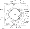
중간영역(MA) 중 스캔라인(SL)들 및 데이터라인(DL)들이 우회하는 영역과 제1영역(OA) 사이에는 하나 또는 그 이상의 세퍼레이터(SP)가 위치할 수 있다. 평면 상에서, 세퍼레이터(SP)들 각각은 제1영역(OA)을 둘러싸는 고리 형상일 수 있으며, 세퍼레이터(SP)들은 상호 이격되어 배치될 수 있다. One or more separators SP may be positioned between the first area OA and the area in which the scan lines SL and data lines DL are bypassed of the intermediate area MA. On a plane, each of the separators SP may have a ring shape surrounding the first area OA, and the separators SP may be disposed to be spaced apart from each other.
도 8은 본 발명의 일 실시예에 따른 표시 패널의 단면도로서, 도 7의 VIII- VIII'선에 따른 단면에 대응할 수 있으며, 도9a 내지 도 9b는 본 발명의 일 실시예에 따른 표시 패널 중 세퍼레이터를 중심으로 한 제조 공정을 나타낸 단면도들이다.8 is a cross-sectional view of a display panel according to an exemplary embodiment of the present invention, and may correspond to a cross section taken along line VIII-VIII' of FIG. 7, and FIGS. 9A to 9B are These are cross-sectional views showing the manufacturing process centered on the separator.
도 8의 표시영역(DA)을 참조하면, 기판(100)은 글래스재 또는 고분자 수지를 포함할 수 있으며, 일 실시예로서 기판(100)은 앞서 도 3a를 참조하여 설명한 바와 같이 다층을 포함할 수 있다. Referring to the display area DA of FIG. 8, the
기판(100) 상에는 불순물이 박막트랜지스터(TFT)의 반도체층(Act)으로 침투하는 것을 방지하기 위해 형성된 버퍼층(201)이 형성될 수 있다. 버퍼층(201)은 실리콘나이트라이드, 실리콘옥시나이트라이드 및 실리콘옥사이드와 같은 무기 절연물을 포함할 수 있으며, 전술한 무기 절연물을 포함하는 단층 또는 다층일 수 있다. A
버퍼층(201) 상에는 화소회로(PC)가 배치될 수 있다. 화소회로(PC)는 박막트랜지스터(TFT) 및 스토리지 커패시터(Cst)를 포함한다. 박막트랜지스터(TFT)는 반도체층(Act), 게이트전극(GE), 소스전극(SE), 드레인전극(DE)을 포함할 수 있다. 도 8에 도시된 박막트랜지스터(TFT)는 도 6을 참조하여 설명한 구동 박막트랜지스터에 대응할 수 있으며, 데이터라인(DL)은 화소회로(PC)에 포함된 스위칭 박막트랜지스터와 전기적으로 연결된다. 본 실시예에서는 게이트전극(GE)이 게이트절연층(203)을 가운데 두고 반도체층(Act) 상에 배치된 탑 게이트 타입을 도시하였으나, 또 다른 실시예에 따르면 박막트랜지스터(TFT)는 바텀 게이트 타입일 수 있다. A pixel circuit PC may be disposed on the
반도체층(Act)은 폴리 실리콘을 포함할 수 있다. 또는, 반도체층(Act)은 비정질(amorphous) 실리콘을 포함하거나, 산화물 반도체를 포함하거나, 유기 반도체 등을 포함할 수 있다. 게이트전극(GE)은 저저항 금속 물질을 포함할 수 있다. 게이트전극(GE)은 몰리브데넘(Mo), 알루미늄(Al), 구리(Cu), 티타늄(Ti) 등을 포함하는 도전 물질을 포함할 수 있고, 상기의 재료를 포함하는 다층 또는 단층으로 형성될 수 있다.The semiconductor layer Act may include polysilicon. Alternatively, the semiconductor layer Act may include amorphous silicon, an oxide semiconductor, or an organic semiconductor. The gate electrode GE may include a low resistance metal material. The gate electrode GE may include a conductive material including molybdenum (Mo), aluminum (Al), copper (Cu), titanium (Ti), etc., and is formed in a multilayer or single layer including the above material. Can be.
반도체층(Act)과 게이트전극(GE) 사이의 게이트절연층(203)은 실리콘옥사이드, 실리콘나이트라이드, 실리콘옥시나이트라이드, 알루미늄옥사이드, 티타늄옥사이드, 탄탈륨옥사이드, 및 하프늄옥사이드 등과 같은 무기 절연물을 포함할 수 있다. 게이트절연층(203)은 전술한 물질을 포함하는 단층 또는 다층일 수 있다.The
소스전극(SE) 및 드레인전극(DE)은 데이터라인(DL)과 동일한 층 상에 위치할 수 있다. 소스전극(SE), 드레인전극(DE), 및 데이터라인(DL)은 전도성이 좋은 재료를 포함할 수 있다. 소스전극(SE) 및 드레인전극(DE)은 몰리브데넘(Mo), 알루미늄(Al), 구리(Cu), 티타늄(Ti) 등을 포함하는 도전 물질을 포함할 수 있고, 상기의 재료를 포함하는 다층 또는 단층으로 형성될 수 있다. 일 실시예로, 소스전극(SE), 드레인전극(DE), 및 데이터라인(DL)은 Ti/Al/Ti의 다층으로 형성될 수 있다. The source electrode SE and the drain electrode DE may be positioned on the same layer as the data line DL. The source electrode SE, the drain electrode DE, and the data line DL may include a material having good conductivity. The source electrode SE and the drain electrode DE may include a conductive material including molybdenum (Mo), aluminum (Al), copper (Cu), titanium (Ti), and the like, and include the above materials. It may be formed as a multi-layer or a single layer. In one embodiment, the source electrode SE, the drain electrode DE, and the data line DL may be formed of a multilayer of Ti/Al/Ti.
스토리지 커패시터(Cst)는 제1층간절연층(205)을 사이에 두고 중첩하는 하부 전극(CE1)과 상부 전극(CE2)을 포함한다. 스토리지 커패시터(Cst)는 박막트랜지스터(TFT)와 중첩될 수 있다. 이와 관련하여, 도 8은 박막트랜지스터(TFT)의 게이트전극(GE)이 스토리지 커패시터(Cst)의 하부 전극(CE1)인 것을 도시하고 있다. 다른 실시예로서, 스토리지 커패시터(Cst)는 박막트랜지스터(TFT)와 중첩하지 않을 수 있다. 스토리지 커패시터(Cst)는 제2층간절연층(207)으로 커버될 수 있다. 스토리지 커패시터(Cst)의 상부 전극(CE2)은 몰리브데넘(Mo), 알루미늄(Al), 구리(Cu), 티타늄(Ti) 등을 포함하는 도전 물질을 포함할 수 있고, 상기의 재료를 포함하는 다층 또는 단층으로 형성될 수 있다.The storage capacitor Cst includes a lower electrode CE1 and an upper electrode CE2 overlapping the first
제1층간절연층(205) 및 제2층간절연층(207)은 실리콘옥사이드, 실리콘나이트라이드, 실리콘옥시나이트라이드, 알루미늄옥사이드, 티타늄옥사이드, 탄탈륨옥사이드, 하프늄옥사이드 등과 같은 무기 절연물을 포함할 수 있다. 제1층간절연층(205) 및 제2층간절연층(207)은 전술한 물질을 포함하는 단층 또는 다층일 수 있다.The first
박막트랜지스터(TFT) 및 스토리지 커패시터(Cst)를 포함하는 화소회로(PC)는 제1유기절연층(209)으로 커버될 수 있다. 제1유기절연층(209)은 상면이 대략 편평한 면을 포함할 수 있다. The pixel circuit PC including the thin film transistor TFT and the storage capacitor Cst may be covered with the first organic insulating
화소회로(PC)는 화소전극(221)과 전기적으로 연결될 수 있다. 예컨대, 도 8에 도시된 바와 같이 박막트랜지스터(TFT)와 화소전극(221) 사이에는 콘택메탈(CM)이 더 개재될 수 있다. 콘택메탈(CM)은 제1유기절연층(209)에 형성된 콘택홀을 통해 박막트랜지스터(TFT)와 접속할 수 있으며, 화소전극(221)은 콘택메탈(CM) 상의 제2유기절연층(211)에 형성된 콘택홀을 통해 콘택메탈(CM)에 접속할 수 있다. 콘택메탈(CM)은 몰리브데넘(Mo), 알루미늄(Al), 구리(Cu), 티타늄(Ti) 등을 포함하는 도전 물질을 포함할 수 있고, 상기의 재료를 포함하는 다층 또는 단층으로 형성될 수 있다. 일 실시예로, 콘택메탈(CM)은 Ti/Al/Ti의 다층으로 형성될 수 있다. The pixel circuit PC may be electrically connected to the
제1유기절연층(209) 및 제2유기절연층(211)은 Polymethylmethacrylate(PMMA)나 Polystylene(PS)과 같은 일반 범용고분자, 페놀계 그룹을 갖는 고분자 유도체, 아크릴계 고분자, 이미드계 고분자, 아릴에테르계 고분자, 아마이드계 고분자, 불소계고분자, p-자일렌계 고분자, 비닐알콜계 고분자, 및 이들의 블렌드와 같은 유기 절연물을 포함할 수 있다. 일 실시예로, 제1유기절연층(209) 및 제2유기절연층(211)은 폴리이미드를 포함할 수 있다. The first organic insulating
화소전극(221)은 제2유기절연층(211) 상에 형성될 수 있다. 도 8에서는 콘택메탈(CM)과 제2유기절연층(211)이 포함된 구조를 설명하고 있으나, 다른 실시예에서 콘택메탈(CM)과 제2유기절연층(211)은 생략될 수 있다. 이 경우, 화소전극(221)은 제1유기절연층(209) 상에 위치하며, 제1유기절연층(209)에 형성된 콘택홀을 통해 화소전극(221)은 박막트랜지스터(TFT)와 전기적으로 연결될 수 있다The
화소전극(221)은 인듐틴옥사이드(ITO; indium tin oxide), 인듐징크옥사이드(IZO; indium zinc oxide), 징크옥사이드(ZnO; zinc oxide), 인듐옥사이드(In2O3: indium oxide), 인듐갈륨옥사이드(IGO; indium gallium oxide) 또는 알루미늄징크옥사이드(AZO; aluminum zinc oxide)와 같은 도전성 산화물을 포함할 수 있다. 다른 실시예로, 화소전극(221)은 은(Ag), 마그네슘(Mg), 알루미늄(Al), 백금(Pt), 팔라듐(Pd), 금(Au), 니켈(Ni), 네오디뮴(Nd), 이리듐(Ir), 크로뮴(Cr) 또는 이들의 화합물을 포함하는 반사막을 포함할 수 있다. 또 다른 실시예로, 화소전극(221)은 전술한 반사막의 위/아래에 ITO, IZO, ZnO 또는 In2O3로 형성된 막을 더 포함할 수 있다. The
화소전극(221) 상에는 화소정의막(215)이 형성될 수 있다. 화소정의막(215)은 화소전극(221)의 상면을 노출하는 개구를 포함하되, 화소전극(221)의 가장자리를 커버할 수 있다. 화소정의막(215)은 유기 절연물을 포함할 수 있다. 또는, 화소정의막(215)은 실리콘나이트라이드(SiNx)나 실리콘옥시나이트라이드(SiON), 또는 실리콘옥사이드(SiOx)와 같은 무기 절연물을 포함할 수 있다. 또는, 화소정의막(215)은 유기절연물 및 무기절연물을 포함할 수 있다.A
중간층(222)은 발광층(222b)을 포함한다. 중간층(222)은 발광층(222b)의 아래에 배치된 제1기능층(222a) 및/또는 발광층(222b)의 위에 배치된 제2기능층(222c)을 포함할 수 있다. 발광층(222b)은 소정의 색상의 빛을 방출하는 고분자 또는 저분자 유기물을 포함할 수 있다. The
제1기능층(222a)은 단층 또는 다층일 수 있다. 예컨대 제1기능층(222a)이 고분자 물질로 형성되는 경우, 제1기능층(222a)은 단층구조인 홀 수송층(HTL: Hole Transport Layer)으로서, 폴리에틸렌 디히드록시티오펜(PEDOT: poly-(3,4)-ethylene-dihydroxy thiophene)이나 폴리아닐린(PANI: polyaniline)으로 형성할 수 있다. 제1기능층(222a)이 저분자 물질로 형성되는 경우, 제1기능층(222a)은 홀 주입층(HIL: Hole Injection Layer)과 홀 수송층(HTL)을 포함할 수 있다.The first
제2기능층(222c)은 언제나 구비되는 것은 아니다. 예컨대, 제1기능층(222a)과 발광층(222b)을 고분자 물질로 형성하는 경우, 제2기능층(222c)을 형성하는 것이 바람직하다. 제2기능층(222c)은 단층 또는 다층일 수 있다. 제2기능층(222c)은 전자 수송층(ETL: Electron Transport Layer) 및/또는 전자 주입층(EIL: Electron Injection Layer)을 포함할 수 있다.The second
중간층(222) 중 발광층(222b)은 표시영역(DA)에서 각 화소마다 배치될 수 있다. 발광층(222b)은 화소정의막(215)의 개구를 통해 노출된 화소전극(221)과 대응하도록 패터닝될 수 있다. 발광층(222b)과 달리, 중간층(222) 중 제1기능층(222a) 및 제2기능층(222c)은 표시영역(DA)뿐만 아니라 중간영역(MA)에도 존재할 수 있다. The
대향전극(223)은 일함수가 낮은 도전성 물질로 이루어질 수 있다. 예컨대, 대향전극(223)은 은(Ag), 마그네슘(Mg), 알루미늄(Al), 백금(Pt), 팔라듐(Pd), 금(Au), 니켈(Ni), 네오디뮴(Nd), 이리듐(Ir), 크로뮴(Cr), 리튬(Li), 칼슘(Ca) 또는 이들의 합금 등을 포함하는 (반)투명층을 포함할 수 있다. 또는, 대향전극(223)은 전술한 물질을 포함하는 (반)투명층 상에 ITO, IZO, ZnO 또는 In2O3과 같은 층을 더 포함할 수 있다. 대향전극(223)은 표시영역(DA)뿐만 아니라 중간영역(MA) 상에도 형성될 수 있다. 제1기능층(222a), 제2기능층(222c), 및 대향전극(223)은 열 증착법에 의해 형성될 수 있다. The
캡핑층(230)은 대향전극(223) 상에 위치할 수 있다. 예컨대, 캡핑층(230)은 LiF를 포함할 수 있으며, 열 증착법에 의해 형성될 수 있다. 일부 실시예에서, 캡핑층(230)은 생략될 수 있다.The
화소정의막(215) 상에는 스페이서(217)가 형성될 수 있다. 스페이서(217)는 폴리이미드와 같은 유기 절연물을 포함할 수 있다. 또는, 스페이서(217)는 실리콘나이트라이드나 실리콘옥사이드와 같은 무기 절연물을 포함하거나, 유기절연물 및 무기절연물을 포함할 수 있다. A
스페이서(217)는 화소정의막(215)과 다른 물질을 포함하거나, 화소정의막(215)과 동일한 물질을 포함할 수 있다. 예컨대, 화소정의막(215)과 스페이서(217)는 하프톤 마스크을 이용한 마스크 공정에서 함께 형성될 수 있다. 일 실시예로서, 화소정의막(215) 및 스페이서(217)는 폴리이미드를 포함할 수 있다.The
유기발광다이오드(OLED)는 박막봉지층(300)으로 커버된다. 박막봉지층(300)은 적어도 하나의 유기봉지층 및 적어도 하나의 무기봉지층을 포함할 수 있으며, 도 8은 박막봉지층(300)이 제1 및 제2무기봉지층(310, 330) 및 이들 사이에 개재된 유기봉지층(320)을 포함하는 것을 도시한다. 다른 실시예에서 유기봉지층의 개수와 무기봉지층의 개수 및 적층 순서는 변경될 수 있다. The organic light emitting diode (OLED) is covered with a thin
제1무기봉지층(310) 및 제2무기봉지층(330)은 알루미늄옥사이드, 티타늄옥사이드, 탄탈륨옥사이드, 하프늄옥사이드, 징크옥사이드, 실리콘옥사이드, 실리콘나이트라이드, 실리콘옥시나이트라이드 하나 이상의 무기물을 포함할 수 있다. 제1무기봉지층(310) 및 제2무기봉지층(330)은 전술한 물질을 포함하는 단일 층 또는 다층일 수 있다. 유기봉지층(320)은 폴리머(polymer)계열의 물질을 포함할 수 있다. 폴리머 계열의 소재로는 아크릴계 수지, 에폭시계 수지, 폴리이미드 및 폴리에틸렌 등을 포함할 수 있다. The first
제1무기봉지층(310) 및 제2무기봉지층(330)의 두께는 서로 다를 수 있다. 제1무기봉지층(310)의 두께가 제2무기봉지층(330)의 두께 보다 클 수 있다. 예컨대, 제1무기봉지층(310)의 두께는 약 1㎛이고, 제2무기봉지층(330)의 두께는 약 0.7㎛일 수 있다. 또는, 제2무기봉지층(330)의 두께가 제1무기봉지층(310)의 두께 보다 크거나, 제1무기봉지층(310) 및 제2무기봉지층(330)의 두께는 서로 동일할 수 있다.The thicknesses of the first
도 8의 중간영역(MA)을 참조하면, 중간영역(MA)은 제1영역(OA)으로부터 상대적으로 먼 제1서브중간영역(SMA1) 및 제1영역(OA)에 상대적으로 가까운 제2서브중간영역(SMA2)을 포함할 수 있다. 중간영역(MA)에는, 제1영역(OA)을 우회하는 라인들 및 세퍼레이터(SP)가 배치될 수 있다. Referring to the middle area MA of FIG. 8, the middle area MA is a first sub relatively far from the first area OA and a second sub relatively close to the first area SMA1 and OA. It may include an intermediate region SMA2. Lines bypassing the first area OA and the separator SP may be disposed in the intermediate area MA.
데이터라인(DL)들은 제1서브중간영역(SMA1)에 위치할 수 있다. 도 8에 도시된 제1서브중간영역(SMA1)의 데이터라인(DL)들은, 앞서 도 7을 참조하여 설명한 우회하는 부분(예컨대, DL-D1, DL-D2)들에 해당한다. 제1서브중간영역(SMA1)은 전술한 데이터라인(DL)들과 같은 라인들이 우회하는 라인영역 또는 우회영역으로 이해될 수 있다. The data lines DL may be located in the first sub intermediate area SMA1. The data lines DL of the first sub-intermediate region SMA1 illustrated in FIG. 8 correspond to the bypassed portions (eg, DL-D1 and DL-D2) described with reference to FIG. 7. The first sub-intermediate area SMA1 may be understood as a line area or a bypass area in which lines such as the above-described data lines DL are bypassed.
데이터라인(DL)들은 절연층을 개재한 채 서로 교번적으로 배치될 수 있다. 예컨대, 이웃하는 데이터라인(DL)들 중 하나는 절연층(예, 제1유기절연층, 209)의 아래에 배치되고 다른 하나는 절연층(예, 제1유기절연층, 209)의 위에 배치되는 것과 같이, 교번적으로 배치된다. 데이터라인(DL)들이 절연층을 사이에 두고 교번적으로 배치되는 경우, 데이터라인들 사이의 거리(d, 피치)를 줄일 수 있다. 도 8에는 제1서브중간영역(SMA1)에 위치하는 데이터라인(DL)들을 도시하고 있으나, 도 7을 참조하여 설명한 스캔라인(SL)들, 예컨대 스캔라인(SL)들의 우회 부분들도 제1서브중간영역(SMA1)에 위치할 수 있다. The data lines DL may be alternately arranged with an insulating layer interposed therebetween. For example, one of the neighboring data lines DL is disposed under the insulating layer (eg, the first organic insulating layer, 209) and the other is disposed above the insulating layer (eg, the first organic insulating layer, 209). As is, they are arranged alternately. When the data lines DL are alternately disposed with the insulating layer therebetween, the distance d and the pitch between the data lines can be reduced. Although FIG. 8 shows the data lines DL located in the first sub-intermediate region SMA1, the bypass portions of the scan lines SL described with reference to FIG. 7, for example, the scan lines SL are also first It may be located in the sub middle area SMA1.
제2서브중간영역(SMA2)에는 하나 또는 그 이상의 세퍼레이터(SP)가 배치될 수 있다. 제2서브중간영역(SMA2)은 세퍼레이터(SP)가 위치하는 영역으로서, 중간층(222)에 포함된 유기물층은 세퍼레이터(SP)에 의해 단절(또는 분리)될 수 있다. 제2서브중간영역(SMA2)은 세퍼레이터영역 또는 유기물층의 단절영역(또는 분리영역)으로 이해될 수 있다.One or more separators SP may be disposed in the second sub intermediate region SMA2. The second sub-intermediate region SMA2 is a region in which the separator SP is located, and the organic material layer included in the
세퍼레이터(SP)는 제2서브중간영역(SMA2)에서 절연층, 예컨대 제2층간절연층(207) 상에 위치할 수 있다. 세퍼레이터(SP)는 중간영역(MA)으로 연장된 제1기능층(222a), 및/또는 제2기능층(222c)을 단절(disconnected)시키거나 또는/및 분리시킬 수 있다. 제1기능층(222a), 및/또는 제2기능층(222c)과 유사하게 대향전극(223) 및/또는 캡핑층(230)도 단절될 수 있다. The separator SP may be positioned on an insulating layer, for example, the second
제1기능층(222a), 제2기능층(222c), 및/또는 대향전극(223)은 열증착법 등에 의해 기판(100) 상에 전체적으로 형성될 수 있는데, 세퍼레이터(SP)는 제1기능층(222a), 제2기능층(222c), 및 대향전극(223)을 형성하는 공정 이전에 형성될 수 있다. 세퍼레이터(SP)가 형성된 이후 증착되는 제1기능층(222a), 제2기능층(222c), 및/또는 대향전극(223)은 세퍼레이터(SP)의 형상에 의해 단절(분리)된 구조를 가질 수 있다. LiF 등을 포함하는 캡핑층(230)도 세퍼레이터(SP)의 형상에 의해 단절(분리)된 구조를 가질 수 있다.The first
세퍼레이터(SP)에 의한 제1기능층(222a), 제2기능층(222c), 대향전극(223), 및/또는 캡핑층(230)의 단절(분리) 구조를 살펴보면 다음과 같다. A structure of disconnection (separation) of the first
도 9a는 제1기능층(222a), 제2기능층(222c), 대향전극(223) 및/또는 캡핑층(230)이 증착되기 이전을 나타내고, 도 9b는 제1기능층(222a), 제2기능층(222c), 대향전극(223) 및/또는 캡핑층(230)이 증착된 이후를 나타낸 단면도이다.9A shows before the first
도 9a를 참조하면, 세퍼레이터(SP)는 상면(SP-T)의 폭(Wt)이 바닥면(SP-B)의 폭(Wb) 보다 큰 형상을 갖는다. 상면(SP-T)과 바닥면(SP-B)을 연결하는 세퍼레이터(SP)의 측면(SP-L)은 역테이퍼진 경사면을 포함할 수 있으며, 이와 관련하여 도 9a는 세퍼레이터(SP)의 측면(SP-L)이 하나의 역테이퍼진 경사면을 포함하며, 세퍼레이터(SP)의 단면이 역사다리꼴인 것을 개시한다. 역테이퍼진 경사면이 기판의 상면(100t)과 이루는 각(α)은 30도 이거나 그보다 작을 수 있다. 세퍼레이터(SP)의 두께(SP-H)는 약 3㎛ 이거나 그보다 클 수 있다. Referring to FIG. 9A, the separator SP has a shape in which the width Wt of the upper surface SP-T is larger than the width Wb of the bottom surface SP-B. The side (SP-L) of the separator (SP) connecting the upper surface (SP-T) and the floor surface (SP-B) may include an inverted tapered inclined surface, and FIG. 9A shows the separator SP. It is disclosed that the side surface SP-L includes one inverted tapered inclined surface, and the cross section of the separator SP is an inverted trapezoid. The angle α formed by the inverted tapered inclined surface with the
세퍼레이터(SP)는 유기물을 포함할 수 있다. 세퍼레이터(SP)는 제1유기절연층(209) 및 제2유기절연층(211)과 다른 유기물을 포함할 수 있다. 세퍼레이터(SP)는 감광성 수지, 예컨대 네거티브 포토레지스트를 포함할 수 있다.The separator SP may contain an organic material. The separator SP may include an organic material different from the first organic insulating
세퍼레이터(SP)는 무기물층(PSV)으로 커버될 수 있으며, 무기물층(PSV)은 세퍼레이터(SP)의 상면(SP-T)과 대응하는 하나 또는 그 이상의 홀(PSV-h)을 포함할 수 있다. 홀(PSV-h)은 표시 패널(10)의 제조 공정 중 또는/및 표시 패널(10)이 제조된 이후에 유기물인 세퍼레이터(SP)에서 발생되는 가스의 배출을 위한 통로가 될 수 있다. 홀(PSV-h)은 아웃 개싱 통로일 수 있다.The separator SP may be covered with an inorganic material layer PSV, and the inorganic material layer PSV may include one or more holes PSV-h corresponding to the upper surface SP-T of the separator SP. have. The hole PSV-h may become a passage for discharging gas generated from the separator SP, which is an organic material, during the manufacturing process of the
홀(PSV-h)을 제외한 무기물층(PSV)의 바디는 세퍼레이터(SP)의 상면(SP-T)의 일부와 세퍼레이터(SP)의 측면(SP-L)을 커버할 수 있다. 무기물층(PSV)의 바디는 세퍼레이터(SP)의 상면(SP-T)으로부터 측면(SP-L)을 커버하도록 연장되며, 세퍼레이터(SP)의 아래에 배치된 절연층, 예컨대 제2층간절연층(207)의 상면과 접촉할 수 있다.The body of the inorganic material layer PSV excluding the hole PSV-h may cover a part of the upper surface SP-T of the separator SP and the side surface SP-L of the separator SP. The body of the inorganic material layer PSV extends to cover the side surface SP-L from the upper surface SP-T of the separator SP, and an insulating layer disposed under the separator SP, for example, a second interlayer insulating layer Can contact the upper surface of (207).
도 9b를 참조하면, 전술한 바와 같이 세퍼레이터(SP) 및 무기물층(PSV)이 형성된 이후에 제1기능층(222a), 제2기능층(222c), 대향전극(223) 및/또는 캡핑층(230)이 형성될 수 있다. 제1기능층(222a), 제2기능층(222c), 대향전극(223) 및/또는 캡핑층(230)은 각각 표시영역(DA) 및 중간영역(MA)에 일체로 형성될 수 있다. 중간영역(MA)에는 세퍼레이터(SP)가 배치되므로, 제1기능층(222a), 및/또는 제2기능층(222c)은 세퍼레이터(SP)를 중심으로 단절될 수 있다. 마찬가지로, 대향전극(223)도 세퍼레이터(SP)를 중심으로 단절될 수 있으며, LiF와 같은 물질을 포함하는 캡핑층(230)도 세퍼레이터(SP)를 중심으로 단절될 수 있다.9B, as described above, after the separator (SP) and the inorganic material layer (PSV) are formed, the first
기판(100) 상에 형성된 층들 중 유기물을 포함하는 층은 수분과 같은 이물의 투습 경로가 될 수 있다. 수분과 같은 이물은 유기발광다이오드(OLED)를 손상시킬 수 있다. 본 발명의 실시예에 따르면, 세퍼레이터(SP)에 의해 유기물층인 제1기능층(222a), 및/또는 제2기능층(222c)이 단절되므로, 제1기능층(222a), 및/또는 제2기능층(222c)의 상면과 나란한 방향(측방향, 또는 x방향)으로 수분이 진행하는 것을 최소화할 수 있다. Among the layers formed on the
일 실시예로, 역테이퍼진 경사면을 갖는 세퍼레이터(SP) 주변에는 제1기능층(222a), 제2기능층(222c), 대향전극(223) 및/또는 캡핑층(230)이 증착되기 어려운 쉐도우 영역이 존재할 수 있다. 쉐도우 영역 및/또는 그 주변에서, 제1기능층(222a), 제2기능층(222c), 대향전극(223) 및/또는 캡핑층(230)의 끝단들은 증착 조건에 따라 다양한 형상의 단면을 가질 수 있다. 예컨대, 제1기능층(222a), 제2기능층(222c), 대향전극(223) 및/또는 캡핑층(230)의 끝단들은 세퍼레이터(SP) 주변에서 얇은 두께를 갖도록 형성될 수 있다. 제1기능층(222a), 제2기능층(222c), 대향전극(223) 및/또는 캡핑층(230)의 끝단들의 위치 및 그 단면 형상은 증착 조건(예, 시간, 증착 방향, 물질 등)에 따라 달라질 수 있다. In one embodiment, it is difficult to deposit the first
본 발명의 비교예로서, 세퍼레이터(SP) 상에 무기물층(PSV)이 없다면, 공정 조건(증착 시간, 증착되는 물질의 입사각 등)에 따라 유기물인 제1기능층 및/또는 제2기능층의 끝단들이 각각 유기물인 세퍼레이터의 측면과 접촉할 가능성이 있다. 서로 접촉한 제1기능층(유기물)과 세퍼레이터(유기물), 및/또는 서로 접촉한 제2기능층(유기물)과 세퍼레이터(유기물)는 새로운 수분의 침투 경로를 형성할 수 있다. 그러나, 본 발명의 실시예에 따르면, 무기물층(PSV)이 세퍼레이터(SP) 상에 배치된 채 세퍼레이터(SP)의 측면(SP-L)등을 커버하므로, 제1기능층(222a) 및/또는 제2기능층(222c)의 끝단들이 세퍼레이터(SP)에 접촉하는 것을 방지할 수 있다. 따라서, 유기물인 제1기능층(222a) 및/또는 제2기능층(222c)과 유기물인 세퍼레이터(SP)가 서로 접촉하며, 투습 경로가 형성되는 것을 방지할 수 있다. As a comparative example of the present invention, if there is no inorganic material layer (PSV) on the separator (SP), depending on the process conditions (deposition time, incident angle of the material to be deposited, etc.), the organic material of the first functional layer and/or the second functional layer It is possible that the ends come into contact with the side of the separator, which is each organic material. The first functional layer (organic material) and the separator (organic material) in contact with each other, and/or the second functional layer (organic material) and the separator (organic material) in contact with each other may form a new moisture penetration path. However, according to an embodiment of the present invention, since the inorganic material layer (PSV) is disposed on the separator (SP) and covers the side surface (SP-L) of the separator (SP), the first functional layer (222a) and / Alternatively, it is possible to prevent the ends of the second
세퍼레이터(SP)는 무기물층(PSV)의 아래에 위치하고, 제1기능층(222a) 및/또는 제2기능층(222c)은 무기물층(PSV)의 위에 위치하는 것과 같이, 무기물층(PSV)에 의해 세퍼레이터(SP)는 제1기능층(222a) 및/또는 제2기능층(222c)과 공간적으로 분리되며, 서로 접촉하지 않을 수 있다. 마찬가지로, 대향전극(223) 및/또는 캡핑층(230)도 무기물층(PSV)에 의해 세퍼레이터(SP)와 분리될 수 있으며, 서로 접촉하지 않을 수 있다. The separator SP is located under the inorganic material layer PSV, and the first
무기물층(PSV)은 금속 또는 무기 절연물을 포함할 수 있다. 예컨대, 무기물층(PSV)은 ITO와 같은 투명도전산화물(TCO, Transparent Conductive Oxide) 또는/및 금속층을 포함할 수 있다. 또는, 무기물층(PSV)은 실리콘옥사이드, 실리콘나이트라이드, 실리콘옥시나이트라이드와 같은 무기 절연물을 포함할 수 있다. The inorganic material layer PSV may include a metal or an inorganic insulating material. For example, the inorganic material layer (PSV) may include a transparent conductive oxide (TCO, Transparent Conductive Oxide) such as ITO or/and a metal layer. Alternatively, the inorganic material layer PSV may include an inorganic insulating material such as silicon oxide, silicon nitride, or silicon oxynitride.
다시 도 8을 참조하면, 기판(100) 상에 복수의 세퍼레이터(SP)들이 배치되는 경우, 세퍼레이터(SP)들은 상호 이격된 채 배치될 수 있으며, 세퍼레이터(SP)들 사이에 격벽(PW)이 위치할 수 있다. 세퍼레이터(SP)들의 높이는 격벽(PW)의 높이와 같거나 그보다 작을 수 있다. 여기서, 세퍼레이터(SP)의 높이 및 격벽(PW)의 높이는, 각각 기판(100)의 상면으로부터 세퍼레이터(SP)의 상면까지의 수직 거리, 및 기판(100)의 상면으로부터 격벽(PW)의 상면까지의 수직 거리일 수 있다.Referring back to FIG. 8, when a plurality of separators SP are disposed on the
유기봉지층(320)은 기판(100)에 모노머를 도포한 후 이를 경화하여 형성할 수 있다. 격벽(PW)은 모노머의 흐름을 제어할 수 있으며, 모노머의 두께, 즉 유기봉지층(320)의 두께를 조절할 수 있다. 유기봉지층(320)의 끝단은 격벽(PW)의 일측에 위치할 수 있다. 격벽(PW)은 제1유기절연층(209), 제2유기절연층(211), 및/또는 화소정의막(215)과 동일한 물질을 포함할 수 있다.The
상대적으로 표시영역(DA)에 인접하게 배치된 세퍼레이터(SP), 예컨대 격벽(PW)과 표시영역(DA)의 유기발광다이오드(OLED) 사이에 위치하는 세퍼레이터(SP)는 유기봉지층(320)으로 커버될 수 있다. The separator SP disposed relatively adjacent to the display area DA, for example, the separator SP disposed between the partition wall PW and the organic light emitting diode OLED of the display area DA, is an
유기봉지층(320)의 아래에 배치된 제1무기봉지층(310)은 화학기상증착법(CVD) 등에 의해 형성될 수 있다. 제1무기봉지층(310)은 제1기능층(222a), 제2기능층(222c), 대향전극(223), 및/또는 캡핑층(230)과 달리 스텝 커버리지가 상대적으로 우수하므로, 제1무기봉지층(310)은 단절되지 않은 채 연속적으로 형성될 수 있다. 예컨대, 제1무기봉지층(310)은 세퍼레이터(SP)의 상면 및 측면을 커버하도록 연속적으로 형성될 수 있다. 제1무기봉지층(310)은 세퍼레이터(SP)에 의해 단절된 제1기능층(222a), 제2기능층(222c) 대향전극(223) 및/또는 캡핑층(230)의 적층체를 커버할 수 있다. The first
제2무기봉지층(330)은 유기봉지층(320) 상에 위치한다. 제2무기봉지층(330)은 제1무기봉지층(310)과 마찬가지로 기판(100)을 전체적으로 커버할 수 있다. 제2무기봉지층(330)의 일 부분은 제2서브중간영역(SMA2)상에서 제1무기봉지층(310)과 직접 접촉할 수 있다. 예컨대, 제2무기봉지층(330)은 제1영역(OA1)과 유기봉지층(320)의 끝단 사이의 영역에서 제1무기봉지층(310)과 직접 접촉할 수 있다. The second
평탄화층(410)은 박막봉지층(300) 상에 위치할 수 있다. 평탄화층(410)은 중간영역(MA) 중 유기봉지층(320)이 존재하지 않는 영역을 커버함으로써, 표시 패널(10)의 편평도를 향상시킬 수 있다. 따라서, 표시 패널(10) 상에 직접 형성되거나 점착층에 의해 결합되는 입력 감지층이나 또는/및 광학 기능층 등이 표시 패널(10)로부터 분리 또는 이탈 것을 방지할 수 있다. The
평탄화층(410)은 유기절연물을 포함할 수 있다. 일 실시예로서, 평탄화층(410)은 박막봉지층(300) 상에 포토레지스트(네거티브 또는 포지티브)이거나 폴리머(polymer)계열의 유기물을 도포하고 이를 패터닝하여 형성할 수 있다. 일 실시예로, 평탄화층(410)은 중간영역(MA)에만 위치할 수 있다. 평면상에서, 평탄화층(410)은 제1영역(OA)을 둘러싸는 고리 형상일 수 있다. The
평탄화층(410) 상에는 제1상부 절연층(420) 및 제2상부 절연층(430)이 형성될 수 있다. 제1상부 절연층(420)은 무기 절연층을 포함하고, 제2상부 절연층(430)은 유기 절연층을 포함할 수 있다. 일 실시예로서, 표시 패널(10) 상에 직접 입력감지층(40, 도 2a 참조)이 형성되는 경우, 제1상부 절연층(420) 및 제2상부 절연층(430)은 각각 입력감지층(40)에 포함된 절연층과 일체로 형성될 수 있다. A first upper insulating
표시 패널(10)은 제1영역(OA)에 대응하는 제1개구(10H)를 포함할 수 있다. 제1개구(10H)는 기판(100) 상에 전술한 구성 요소들이 형성된 이후에 제1라인(SCL)을 따라 커팅 또는 스크라이빙 공정 등이 진행함으로써 형성될 수 있다. 제1개구(10H)의 측면은 제1개구(10H)를 향해 노출된 기판(100)의 측면, 및 그 위에 적층된 층들의 측면들을 포함할 수 있다.The
도 8을 참조하여 설명한 세퍼레이터(SP)는 무기 절연층인 제2층간절연층(207) 상에 직접 배치된 것을 도시하나, 본 발명은 이에 한정되지 않는다. 다른 실시예로서, 도 10 및 도 11을 참조하여 후술하는 바와 같이 세퍼레이터(SP)의 아래에는 다양한 구조를 갖는 구성요소가 배치될 수 있다. The separator SP described with reference to FIG. 8 is shown directly disposed on the second
도 10은 본 발명의 다른 실시예에 따른 세퍼레이터 및 그 주변의 구조를 나타낸 단면도이다. 도 10에서는 편의상 캡핑층(230) 위의 구성요소, 예컨대 도 8을 참조하여 설명한 박막봉지층(300) 및 그 위의 구성요소를 생략한다10 is a cross-sectional view showing a separator and a structure around the separator according to another embodiment of the present invention. In FIG. 10, for convenience, the components above the
도 10을 참조하면, 세퍼레이터(SP)의 아래에 금속층(ML)이 배치될 수 있다. 금속층(ML)은 무기 절연층(예, 제2층간절연층, 207)과 세퍼레이터(SP) 사이에 배치된다. 세퍼레이터(SP)는 금속층(ML)의 상면과 직접 접촉할 수 있다. 금속층(ML)과 세퍼레이터(SP) 사이의 점착력(adhesion)은 무기 절연층(예, 제2층간절연층, 207)과 세퍼레이터(SP) 사이의 점착력에 비하여 우수할 수 있다. Referring to FIG. 10, a metal layer ML may be disposed under the separator SP. The metal layer ML is disposed between the inorganic insulating layer (eg, the second interlayer insulating layer 207) and the separator SP. The separator SP may directly contact the upper surface of the metal layer ML. The adhesion between the metal layer ML and the separator SP may be superior to that between the inorganic insulating layer (eg, the second interlayer insulating layer 207) and the separator SP.
금속층(ML)은 앞서 도 8을 참조하여 설명한 화소회로(PC)의 소스전극(SE), 드레인전극(DE), 데이터라인(DL)과 동일한 물질을 포함할 수 있다. 또는, 금속층(ML)은 앞서 도 8을 참조하여 설명한 콘택메탈(CM)과 동일한 물질을 포함할 수 있다. The metal layer ML may include the same material as the source electrode SE, the drain electrode DE, and the data line DL of the pixel circuit PC described above with reference to FIG. 8. Alternatively, the metal layer ML may include the same material as the contact metal CM described with reference to FIG. 8.
세퍼레이터(SP)는 네거티브 포토레지스트와 같이 감광성 물질을 포함할 수 있으며, 전술한 물질을 포함하는 세퍼레이터(SP)를 형성하는 공정은 노광, 현상, 및 베이크 공정을 포함할 수 있다. 세퍼레이터(SP)를 형성하기 위한 노광 공정 시, 빛은 금속층(ML)에 반사될 수 있다. 금속층(ML)에 의한 빛의 반사를 고려하여, 금속층(ML)의 폭(W1)은 세퍼레이터(SP)의 상면(SP-T)의 폭(Wt)과 같거나 그 보다 크게 선택될 수 있다 (Wb < Wt ≤ W1). The separator SP may include a photosensitive material such as a negative photoresist, and a process of forming the separator SP including the above-described material may include exposure, development, and baking processes. During the exposure process for forming the separator SP, light may be reflected on the metal layer ML. In consideration of reflection of light by the metal layer ML, the width W1 of the metal layer ML may be selected equal to or greater than the width Wt of the upper surface SP-T of the separator SP ( Wb <Wt ≤ W1).
무기물층(PSV)은 세퍼레이터(SP)의 상면(SP-T)의 일부와 측면(SP-L)을 커버할 수 있으며, 금속층(ML)을 커버할 수 있다. 무기물층(PSV)은 세퍼레이터(SP)와 금속층(ML)을 커버한 채 금속층(ML)의 아래에 배치된 무기 절연층(예, 제2층간절연층, 207) 상으로 연장될 수 있다. 무기물층(PSV)은 세퍼레이터(SP)의 상면(SP-T)의 일부와 측면(SP-L), 금속층(ML)의 상면(ML-T)의 일부와 측면(ML-L), 그리고 제2층간절연층(207)과 접촉할 수 있다. 세퍼레이터(SP)의 상면(SP-T) 중 무기물층(PSV)으로 커버되지 않은 부분은 아웃 개싱을 위한 홀(PSV-h)이 위치하는 영역에 해당한다. The inorganic material layer PSV may cover a part of the upper surface SP-T and the side surface SP-L of the separator SP, and may cover the metal layer ML. The inorganic material layer PSV may extend onto the inorganic insulating layer (eg, the second interlayer insulating layer 207) disposed under the metal layer ML while covering the separator SP and the metal layer ML. The inorganic material layer (PSV) is a part of the upper surface (SP-T) of the separator (SP) and a side surface (SP-L), a part of the upper surface (ML-T) of the metal layer (ML) and the side surface (ML-L), and It may be in contact with the interlayer insulating
도 11은 본 발명의 다른 실시예에 따른 세퍼레이터 및 그 주변의 구조를 나타낸 단면도이다. 도 11은 편의상 캡핑층(230) 위의 구성요소, 예컨대 도 8을 참조하여 설명한 박막봉지층(300) 및 그 위의 구성요소를 생략한다. 11 is a cross-sectional view showing a separator and a structure around the separator according to another embodiment of the present invention. In FIG. 11, for convenience, the components above the
도 11을 참조하면, 세퍼레이터(SP)의 아래에 유기층(OL)이 배치될 수 있다. 유기층(OL)은 무기 절연층(예, 제2층간절연층, 207)과 세퍼레이터(SP) 사이에 배치된다. 세퍼레이터(SP)는 유기층(OL)의 상면과 직접 접촉할 수 있다. 유기층(OL)과 세퍼레이터(SP) 사이의 점착력(adhesion)은 무기 절연층(예, 제2층간절연층, 207)과 세퍼레이터(SP) 사이의 점착력에 비하여 우수할 수 있다. Referring to FIG. 11, an organic layer OL may be disposed under the separator SP. The organic layer OL is disposed between the inorganic insulating layer (eg, the second interlayer insulating layer 207) and the separator SP. The separator SP may directly contact the upper surface of the organic layer OL. The adhesion between the organic layer OL and the separator SP may be superior to that between the inorganic insulating layer (eg, the second interlayer insulating layer 207) and the separator SP.
유기층(OL)은 앞서 도 8을 참조하여 설명한 제1유기절연층(209) 또는 제2유기절연층(211)과 동일한 물질을 포함할 수 있다. 유기층(OL)은 제1유기절연층(209) 또는 제2유기절연층(211)과 동일한 공정에서 형성될 수 있다. 유기층(OL)은 세퍼레이터(SP)의 아래에 존재하도록 패터닝될 수 있다. 도 7을 참조하여 설명한 바와 같이, 평면상에서 세퍼레이터(SP)는 제1영역(OA)을 둘러싸는 고리 형상일 수 있는데, 유기층(OL)도 세퍼레이터(SP)와 마찬가지로 평면상에서 제1영역(OA)을 둘러싸는 고리 형상일 수 있다. 유기층(OL)의 상면(OL-T)의 폭(W2)은 세퍼레이터(SP)의 바닥면(SP-B)의 폭(Wb)과 같거나 그보다 클 수 있다. The organic layer OL may include the same material as the first organic insulating
무기물층(PSV)은 세퍼레이터(SP)의 상면(SP-T)의 일부와 측면(SP-L)을 커버할 수 있으며, 유기층(OL)을 커버할 수 있다. 무기물층(PSV)은 세퍼레이터(SP)와 유기층(OL)을 커버한 채 유기층(OL)의 아래에 배치된 무기 절연층(예, 제2층간절연층, 207) 상으로 연장될 수 있다. 무기물층(PSV)은 세퍼레이터(SP)의 상면(SP-T)의 일부와 측면(SP-L), 유기층(OL)의 상면(OL-T)의 일부와 측면(OL-L), 그리고 제2층간절연층(207)과 접촉할 수 있다. 세퍼레이터(SP)의 상면(SP-T) 중 무기물층(PSV)으로 커버되지 않은 부분은 아웃 개싱을 위한 홀(PSV-h)이 위치하는 영역에 해당한다. The inorganic material layer PSV may cover a part of the upper surface SP-T and the side surface SP-L of the separator SP, and may cover the organic layer OL. The inorganic material layer PSV may extend onto the inorganic insulating layer (eg, the second interlayer insulating layer 207) disposed under the organic layer OL while covering the separator SP and the organic layer OL. The inorganic material layer (PSV) is a part of the upper surface (SP-T) of the separator (SP) and a side surface (SP-L), a part of the upper surface (OL-T) of the organic layer (OL) and a side surface (OL-L), and It may be in contact with the interlayer insulating
무기물층(PSV)이 유기층(OL)을 커버함으로써, 제1기능층(222a), 제2기능층(222c), 대향전극(223) 및/또는 캡핑층(230)의 끝단들이 유기층(OL)과 접촉하는 것을 방지할 수 있다. 본 발명의 비교예로서 유기물인 제1기능층(222a)과 제2기능층(222c)의 끝단들이 유기층(OL)과 접촉하는 경우, 투습 경로가 형성될 수 있으나, 본 발명의 실시예에 따르면 유기층(OL)과 제1기능층(222a) 및 제2기능층(222c) 사이에 무기물층(PSV)이 배치됨으로써, 전술한 투습 경로의 형성을 차단할 수 있다.Since the inorganic material layer PSV covers the organic layer OL, the ends of the first
도 8 내지 도 11은 세퍼레이터(SP)의 측면(SP-L)이 하나의 경사면, 즉 역테이퍼진 하나의 경사면을 갖는 역 사다리꼴인 것을 도시하나, 본 발명은 이에 한정되지 않는다. 다른 실시예로서, 세퍼레이터(SP)의 측면(SP-L)은 서로 다른 경사각을 갖는 복수의 경사면을 포함할 수 있다.8 to 11 illustrate that the side surface SP-L of the separator SP is an inverted trapezoid having one inclined surface, that is, an inverted tapered inclined surface, but the present invention is not limited thereto. As another embodiment, the side surfaces SP-L of the separator SP may include a plurality of inclined surfaces having different inclination angles.
도 12a 내지 도 12c는 본 발명의 다른 실시예에 따른 세퍼레이터를 나타낸 단면도들이다.12A to 12C are cross-sectional views illustrating a separator according to another embodiment of the present invention.
도 12a를 참조하면, 세퍼레이터(SP)는 상면(SP-T)의 폭(Wt)이 바닥면(SP-B)의 폭(Wb) 보다 크되, 측면(SP-L)이 복수의 서브측면들을 포함할 수 있다. 예컨대, 세퍼레이터(SP)의 측면(SP-L)은 제1서브측면(SP-L1), 제2서브측면(SP-L2), 및 제3서브측면(SP-L3)을 포함할 수 있다. 세퍼레이터(SP)의 상면(SP-T)에서 바닥면(SP-B)을 향하는 방향을 따라, 경사각이 다른 제1서브측면(SP-L1), 제2서브측면(SP-L2), 및 제3서브측면(SP-L3)이 배치될 수 있다. 12A, the separator SP has a width Wt of the upper surface SP-T greater than the width Wb of the bottom surface SP-B, but the side surface SP-L includes a plurality of sub-sides. Can include. For example, the side surface SP-L of the separator SP may include a first sub side surface SP-L1, a second sub side surface SP-L2, and a third sub side surface SP-L3. Along the direction from the top surface (SP-T) of the separator (SP) toward the bottom surface (SP-B), the first sub-side surface (SP-L1), the second sub-side surface (SP-L2), and the Three sub-sides (SP-L3) may be disposed.
일 실시예로, 제2서브측면(SP-L2)의 경사각은 제1서브측면(SP-L1)의 경사각 보다 작고, 제3서브측면(SP-L3)의 경사각은 제2서브측면(SP-L2)의 경사각 보다 크게 형성될 수 있다. 여기서, 제1서브측면(SP-L1), 제2서브측면(SP-L2), 및 제3서브측면(SP-L3) 각각의 경사각은, 각각의 제1서브측면(SP-L1), 제2서브측면(SP-L2), 및 제3서브측면(SP-L3)과 기판의 상면(100t)이 이루는 각으로 이해할 수 있다.In one embodiment, the inclination angle of the second sub-side (SP-L2) is smaller than that of the first sub-side (SP-L1), and the inclination angle of the third sub-side (SP-L3) is the second sub-side (SP- It may be formed larger than the inclination angle of L2). Here, the inclination angle of each of the first sub-side (SP-L1), the second sub-side (SP-L2), and the third sub-side (SP-L3) is, respectively, the first sub-side (SP-L1), It can be understood as an angle formed by the second sub-side (SP-L2) and the third sub-side (SP-L3) and the upper surface (100t) of the substrate.
제1서브측면(SP-L1), 제2서브측면(SP-L2), 및 제3서브측면(SP-L3) 중 적어도 하나의 서브측면은 경사각이 약 30°이거나 그보다 작을 수 있다. 예컨대, 제2서브측면(SP-L2)의 경사각(α)이 30°이거나 그보다 작을 수 있다. At least one of the first sub-side (SP-L1), the second sub-side (SP-L2), and the third sub-side (SP-L3) may have an inclination angle of about 30° or less. For example, the inclination angle α of the second sub-side surface SP-L2 may be 30° or less.
도 12a에는 제1서브측면(SP-L1)의 경사각이 약 90°인 것을 도시하고 있으나, 다른 실시예로서 도 12b에 도시된 바와 같이 제1서브측면(SP-L1)의 경사각은 예각일 수 있다. 12A shows that the inclination angle of the first sub-side (SP-L1) is about 90°, but as another embodiment, as shown in FIG. 12B, the inclination angle of the first sub-side (SP-L1) may be an acute angle. have.
도 12a 및 도 12b는 세퍼레이터(SP)의 측면(SP-L)이 복수의 역테이퍼진 경사면들을 포함하는 것을 도시하나 본 발명은 이에 한정되지 않는다. 도 12c에 도시된 바와 같이 세퍼레이터(SP)의 측면(SP-L)은 역테이퍼진 제1서브측면(SP-L1) 및 순테이퍼진 제2서브측면(SP-L2)을 포함할 수 있다. 역테이퍼진 제1서브측면(SP-L1)의 경사각(α)은 30°이거나 그보다 작을 수 있다.12A and 12B illustrate that the side surface SP-L of the separator SP includes a plurality of inverted tapered inclined surfaces, but the present invention is not limited thereto. As shown in FIG. 12C, the side surface SP-L of the separator SP may include a reverse tapered first sub-side SP-L1 and a purely tapered second sub-side SP-L2. The inclination angle α of the reverse tapered first sub-side SP-L1 may be 30° or less.
도 12a 내지 도 12c 에 도시된 실시예(들), 또는 이로부터 파생되는 실시예(들)에 따른 세퍼레이터(SP)의 구조는 앞서 도 8 내지 도 11을 참조하여 설명한 실시예(들) 및 이들로부터 파생되는 실시예에 적용될 수 있다. 또한, 도 13 내지 도 21을 참조하여 후술할 실시예(들) 및 이들로부터 파생되는 실시예에도 적용될 수 있다.The structure of the separator (SP) according to the embodiment(s) shown in FIGS. 12A to 12C or the embodiment(s) derived therefrom is the embodiment(s) described with reference to FIGS. 8 to 11 above and It can be applied to an embodiment derived from In addition, it may be applied to embodiment(s) to be described later with reference to FIGS. 13 to 21 and an embodiment derived therefrom.
도 13 내지 도 15는 본 발명의 다른 실시예에 따른 표시 패널의 일부를 나타낸 단면도들이다.13 to 15 are cross-sectional views illustrating a part of a display panel according to another exemplary embodiment of the present invention.
세퍼레이터(SP)는, 세퍼레이터(SP)의 측면(SP-L)이 복수의 경사면을 갖거나, 세퍼레이터(SP)의 측면(SP-L)이 비교적 작은 경사각(예컨대, 20°이하, 15°이하 등)을 갖거나, 또는/및 역테이퍼진 경사면과 순테이퍼진 경사면이 교번적으로 형성되는 것과 같이 다양한 형상을 가질 수 있다. In the separator SP, the side surface SP-L of the separator SP has a plurality of inclined surfaces, or the side surface SP-L of the separator SP has a relatively small inclination angle (e.g., 20° or less, 15° or less. Etc.), or/and may have various shapes such as alternately formed inverted tapered slopes and forward tapered slopes.
세퍼레이터(SP)의 형상에 의해 쉐도우 영역이 넓게 형성되는 경우, 도 13에 도시된 바와 같이 제1기능층(222a), 제2기능층(222c), 대향전극(223), 및/또는 캡핑층(230) 각각의 끝단은 세퍼레이터(SP)와 소정의 간격으로 이격될 수 있다. 예컨대, When the shadow region is formed wide by the shape of the separator SP, as shown in FIG. 13, the first
세퍼레이터(SP)에 의해 단절(분리)된 제1기능층(222a), 제2기능층(222c), 대향전극(223), 및/또는 캡핑층(230) 상에는 제1무기봉지층(310)이 형성될 수 있다. 제1무기봉지층(310)은 세퍼레이터(SP)의 측면(SP-L)과 직접 접촉할 수 있다. 또한, 제1무기봉지층(310)은 제1기능층(222a), 제2기능층(222c), 대향전극(223), 및/또는 캡핑층(230)의 끝단들과 세퍼레이터(SP) 사이의 제1이격영역(RA)을 통해 무기 절연층인 제2층간절연층(207)과 직접 접촉할 수 있다.The first
도 14를 참조하면, 금속층(ML)이 세퍼레이터(SP)의 아래에 배치될 수 있다. 금속층(ML)의 폭은 도 10을 참조하여 설명한 바와 같이 세퍼레이터(SP)의 상면의 폭(Wt)과 같거나 그보다 클 수 있다. 제1기능층(222a), 제2기능층(222c), 대향전극(223), 및/또는 캡핑층(230)의 끝단들과 세퍼레이터(SP) 사이의 제1이격영역(RA)에서, 제1무기봉지층(310)은 금속층(ML)과 접촉할 수 있다.Referring to FIG. 14, the metal layer ML may be disposed under the separator SP. As described with reference to FIG. 10, the width of the metal layer ML may be equal to or greater than the width Wt of the upper surface of the separator SP. In the first separation area RA between the ends of the first
도 15를 참조하면, 유기층(OL)이 세퍼레이터(SP)의 아래에 배치될 수 있다. 유기층(OL)의 폭은 세퍼레이터(SP)의 상면의 폭(Wt) 보다 작게 형성될 수 있다. 유기층(OL)의 폭은, 제1기능층(222a), 제2기능층(222c), 대향전극(223), 및/또는 캡핑층(230)의 끝단들과 유기층(OL) 사이에 제2이격영역(RA')이 구비되도록 형성될 수 있다. 제2이격영역(RA')의 폭은 제1이격영역(RA)의 폭과 동일하거나, 제1이격영역(RA)의 폭의 0.7배 이상이거나, 0.8배 이상이거나, 0.9배 이상일 수 있다.Referring to FIG. 15, the organic layer OL may be disposed under the separator SP. The width of the organic layer OL may be smaller than the width Wt of the upper surface of the separator SP. The width of the organic layer OL is the second between the ends of the first
도 16은 본 발명의 다른 실시예에 따른 표시 패널의 일부를 발췌하여 나타낸 단면도이다. 도 16은 편의상 박막봉지층 및 그 위의 구성요소를 생략하고 도시한다.16 is a cross-sectional view illustrating a part of a display panel according to another exemplary embodiment of the present invention. 16 shows the thin film encapsulation layer and the components thereon omitted for convenience.
세퍼레이터(SP) 아래에 위치하는 적어도 하나의 절연층은 그루브(또는 트렌치)를 포함할 수 있다. 이와 관련하여, 도 16은 세퍼레이터(SP) 아래의 제2층간절연층(207)이 그루브(207G)를 포함하는 것을 도시한다. 제2층간절연층(207)은 단일 층이거나 실리콘나이트라이드층과 실리콘옥사이드층을 포함하는 다층일 수 있다. 그루브(207G)의 깊이(d)는 제2층간절연층(207)의 두께(t) 보다 작을 수 있다. 그루브(207G)는 하프톤 마스크 등을 이용하여 형성될 수 있다.At least one insulating layer positioned under the separator SP may include a groove (or trench). In this regard, FIG. 16 shows that the second
그루브(207G)에 의해 제2층간절연층(207)의 상면(270t)과 그루브(207G)의 바닥면(207Gb)은 단차 구조를 형성한다. 전술한 단차 구조에 의해 제1기능층(222a), 제2기능층(222c), 대향전극(223), 및/또는 캡핑층(230)은 더욱 효과적으로 단절될 수 있다. 예컨대, 제1기능층(222a), 제2기능층(222c), 대향전극(223), 및/또는 캡핑층(230)의 끝단들은 제2층간절연층(207)의 상면(207t)의 가장자리(207te)에 위치하고, 그루브(207G)에는 잔여물(RD)이 위치할 수 있다. The upper surface 270t of the second
제1기능층(222a), 제2기능층(222c), 대향전극(223), 및/또는 캡핑층(230)을 형성하는 증착 공정에서 비스듬하게 입사하는 증착물질은 그루브(207G) 내에 위치하여 잔여물(RD)을 형성할 수 있다. 제2층간절연층(207)의 단차 구조에 의해 잔여물(RD)과 제1기능층(222a), 제2기능층(222c), 대향전극(223), 및/또는 캡핑층(230)의 끝단들은 서로 이격될 수 있다. 실시예에 따라 유기물을 포함하는 잔여물(RD)이 유기물인 세퍼레이터(SP)와 접촉한다 하더라도, 세퍼레이터(SP)와 제1기능층(222a), 제2기능층(222c), 대향전극(223), 및/또는 캡핑층(230)의 끝단들은 상호 이격된 구조를 유지할 수 있으므로, 투습에 의한 유기발광소자의 손상을 효과적으로 방지할 수 있다.In the deposition process of forming the first
전술한 투습의 문제는 아래의 조건들 중 적어도 하나 이상을 만족하는 경우에 더욱 효과적으로 방지될 수 있다. The above-described problem of moisture permeation can be more effectively prevented when at least one of the following conditions is satisfied.
세퍼레이터(SP)의 측면(SP-L)이 30°이거나 그보다 작은 경사면을 포함할 수 있다(조건 1). 세퍼레이터(SP)와 이웃한 세퍼레이터(SP) 사이의 제1이격거리(I1)와 세퍼레이터(SP)의 바닥면의 폭(Wb)의 합(I1+ Wb)은 약 6㎛이거나 그 보다 클 수 있다(조건 2). 세퍼레이터(SP)의 두께(SP-H)는 약 3㎛이거나 그보다 클 수 있다(조건 3). 및/또는, 그루브(207G)를 정의하는 제2층간절연층(207)의 내측면과 전술한 내측면과 마주보는 세퍼레이터(SP)의 측면(SP-L) 사이의 제2이격거리(I2)는 약 2㎛이거나 그보다 클 수 있다(조건 4). The side surface SP-L of the separator SP may include an inclined surface of 30° or less (condition 1). The sum (I1+Wb) of the first separation distance I1 between the separator SP and the neighboring separator SP and the width Wb of the bottom surface of the separator SP may be about 6 μm or greater ( Condition 2). The thickness SP-H of the separator SP may be about 3 μm or greater (condition 3). And/or, a second separation distance I2 between the inner side surface of the second
전술한 조건들을 모두 만족하는 경우, 제1기능층(222a), 제2기능층(222c), 대향전극(223), 및/또는 캡핑층(230)을 형성하는 증착 공정의 조건에 구애받지 않고 제1기능층(222a), 제2기능층(222c), 대향전극(223), 및/또는 캡핑층(230)의 끝단이 세퍼레이터(SP)와 이격될 수 있으며, 전술한 투습의 문제를 효과적으로 해결할 수 있다.When all the above-described conditions are satisfied, regardless of the conditions of the deposition process for forming the first
도 17은 본 발명의 다른 실시예에 따른 표시 패널을 나타낸 단면도이다. 도 8을 참조하여 설명한 표시 패널(10)은 이웃한 세퍼레이터(SP) 사이에 격벽(PW)이 배치되며, 유기봉지층(320)의 끝단이 격벽(PW)의 일측에 위치하는 것을 도시하고 있으나, 도 17을 참조하면 세퍼레이터(SP)는 도 8을 참조하여 설명한 격벽(PW)의 기능을 가질 수 있다. 유기봉지층(320)의 끝단은 어느 하나의 세퍼레이터(SP)의 일측에 위치할 수 있다. 17 is a cross-sectional view illustrating a display panel according to another exemplary embodiment of the present invention. In the
도 17을 참조하여 설명한 특징은 도 8 내지 도 16을 참조하여 설명한 전술한 실시예(들), 또는/및 도 18 내지 도 21을 참조하여 후술할 실시예(들)에도 적용될 수 있음은 물론이다.It goes without saying that the features described with reference to FIG. 17 may also be applied to the above-described embodiment(s) described with reference to FIGS. 8 to 16, or/and the embodiment(s) to be described later with reference to FIGS. 18 to 21. .
도 18은 본 발명의 다른 실시예에 따른 표시 패널을 나타낸 단면도이다.18 is a cross-sectional view illustrating a display panel according to another exemplary embodiment of the present invention.
도 18을 참조하면, 무기물층(PSV)은 화소전극(221)과 동일한 물질을 포함할 수 있다. 예컨대, 도 18의 확대도와 같이, 무기물층(PSV)은 제1서브-무기물층(PSV-1), 제2서브-무기물층(PSV-2), 및 제3서브-무기물층(PSV-3)을 포함할 수 있다. Referring to FIG. 18, the inorganic material layer PSV may include the same material as the
도 8을 참조하여 설명한 바와 같이 화소전극(221)은 반사막인 제2서브화소전극층(221-2)의 아래와 위에 각각 배치된 제1서브화소전극층(221-1) 및 제3서브화소전극층(221-3)을 포함할 수 있다. 예컨대, 제2서브화소전극층(221-2)은 은(Ag)을 포함하고, 제1서브화소전극층(221-1) 및 제3서브화소전극층(221-3)은 ITO와 같은 투명도전산화물(TCO)을 포함할 수 있다. 무기물층(PSV)의 제1서브-무기물층(PSV-1), 제2서브-무기물층(PSV-2), 및 제3서브-무기물층(PSV-3)은 각각 제1서브화소전극층(221-1), 제2서브화소전극층(221-2), 및 제3서브화소전극층(221-3)과 동일한 물질을 포함할 수 있다.As described with reference to FIG. 8, the
도 18에서는 세퍼레이터(SP)가 제2층간절연층(207) 상에 위치하는 것을 도시하나 본 발명은 이에 한정되지 않는다. 도 10 및 도 11을 참조하여 설명한 바와 같이 세퍼레이터(SP) 아래에는 금속층이 위치하거나, 유기층이 위치할 수 있다. 도 18에 도시된 세퍼레이터(SP)는 앞서 도 12a 내지 도 12c를 참조하여 설명한 바와 같은 형상 또는 이로부터 파생되는 형상을 가질 수 있다. 도 18의 제2층간절연층(207)은 도 16을 참조하여 설명한 바와 같이 세퍼레이터(SP)가 위치하는 그루브를 포함할 수 있다.18 illustrates that the separator SP is positioned on the second
도 19는 본 발명의 다른 실시예에 따른 표시 패널을 나타낸 단면도이다.19 is a cross-sectional view illustrating a display panel according to another exemplary embodiment of the present invention.
도 19를 참조하면, 세퍼레이터(SP)는 제1층간절연층(205) 상에 위치할 수 있으며, 세퍼레이터(SP)의 상면의 일부와 측면을 커버하는 무기물층(PSV)은 제2층간절연층(207)을 포함할 수 있다. 예컨대, 제2층간절연층(207)이 무기물층(PSV)일 수 있다. 또는, 무기물층(PSV)이 제2층간절연층(207)을 포함하는 것으로 이해할 수 있다. 무기물층(PSV)은 절연성 물질, 예컨대 실리콘옥사이드, 실리콘나이트라이드, 실리콘옥시나이트라이드와 같은 무기 절연물을 포함할 수 있다. 무기물층(PSV)은 전술한 물질의 다층 구조일 수 있다. Referring to FIG. 19, the separator SP may be positioned on the first
무기물층(PSV)은 기판(100) 상에 전체적으로 형성되되, 세퍼레이터(SP)의 상면의 일부와 측면을 커버할 수 있다. 무기물층(PSV)은 세퍼레이터(SP)의 상면에 대응하는 홀(PSV-h)을 포함할 수 있다.The inorganic material layer PSV is formed entirely on the
세퍼레이터(SP)의 아래에는 금속층(ML)이 배치될 수 있으며, 금속층(ML)의 폭과 같은 특징은 앞서 도 10을 참조하여 설명한 바와 같다. 금속층(ML)은 화소회로(PC)를 이루는 박막트랜지스터와 스토리지 커패시터 중 금속을 포함하는 전극과 동일한 물질을 포함할 수 있다. 예컨대, 금속층(ML)은 스토리지 커패시터(Cst)의 상부 전극(CE2)과 동일한 물질을 포함할 수 있으며, 동일한 공정에서 형성될 수 있다.The metal layer ML may be disposed under the separator SP, and features such as the width of the metal layer ML are as described above with reference to FIG. 10. The metal layer ML may include the same material as an electrode including a metal among the thin film transistors and storage capacitors constituting the pixel circuit PC. For example, the metal layer ML may include the same material as the upper electrode CE2 of the storage capacitor Cst, and may be formed in the same process.
세퍼레이터(SP)를 커버하는 무기물층(PSV)에 의해 제1기능층(222a), 제2기능층(222c), 대향전극(223) 및 캡핑층(230)의 끝단들은 세퍼레이터(SP)와 접촉하지 않을 수 있음은 앞서 설명한 바와 같다. 격벽(PW)은 세퍼레이터(SP)와 다른 층 상에 배치될 수 있다. The ends of the first
도 19는 세퍼레이터(SP)의 아래에 금속층(ML)이 배치된 것을 도시하나, 다른 실시예로서 금속층(ML)은 생략될 수 있다. 또는, 금속층(ML) 대신에 앞서 도 11을 참조하여 설명한 바와 같이 유기층이 배치될 수 있다. 도 19에 도시된 세퍼레이터(SP)는 앞서 도 12a 내지 도 12c를 참조하여 설명한 바와 같은 형상 또는 이로부터 파생되는 형상을 가질 수 있다. 및/또는 도 19에 도시된 제1층간절연층(205)은 도 16을 참조하여 설명한 제2층간절연층(207)에 형성된 그루브와 동일한 구조의 그루브를 포함할 수 있다.19 illustrates that the metal layer ML is disposed under the separator SP, but as another embodiment, the metal layer ML may be omitted. Alternatively, instead of the metal layer ML, an organic layer may be disposed as described above with reference to FIG. 11. The separator SP illustrated in FIG. 19 may have a shape as described above with reference to FIGS. 12A to 12C or a shape derived therefrom. And/or the first
도 20은 본 발명의 다른 실시예에 따른 표시 패널을 나타낸 단면도이다.20 is a cross-sectional view illustrating a display panel according to another exemplary embodiment of the present invention.
도 20을 참조하면, 세퍼레이터(SP)는 제2층간절연층(207) 상에 위치할 수 있으며, 세퍼레이터(SP)는 세퍼레이터(SP)의 상면과 대응하는 홀(PSV-h)을 갖는 무기물층(PSV)으로 커버될 수 있다. 무기물층(PSV)은 세퍼레이터(SP)의 상면의 일부 및 측면을 커버하며, 표시영역(DA)으로 연장될 수 있다. 예컨대, 무기물층(PSV)은 기판(100) 상에 전체적으로 형성될 수 있으며, 무기물층(PSV)은 표시영역(DA) 및 제1중간영역(SMA1)에 위치한 데이터라인(DL)들, 박막트랜지스터(TFT)의 소스전극(SE) 및/또는 드레인전극(DE)을 커버할 수 있다. 무기물층(PSV)은 표시영역(DA) 및 제1중간영역(SMA1)에서 데이터라인(DL)들과 접촉할 수 있다. 무기물층(PSV)은 절연성 무기물을 포함할 수 있다. Referring to FIG. 20, the separator SP may be positioned on the second
세퍼레이터(SP)의 아래에는 금속층(ML)이 배치될 수 있으며, 금속층(ML)의 폭과 같은 특징은 앞서 도10을 참조하여 설명한 바와 같다. 금속층(ML)은 화소회로(PC)를 이루는 박막트랜지스터 및 스토리지 커패시터의 전극들 중 어느 하나와 동일한 물질을 포함할 수 있다. 예컨대, 금속층(ML)은 화소회로(PC)에 포함된 데이터라인(DL), 박막트랜지스터(TFT)의 소스전극(SE) 및/또는 드레인전극(DE)과 동일한 물질을 포함할 수 있다.The metal layer ML may be disposed under the separator SP, and features such as the width of the metal layer ML are as described above with reference to FIG. 10. The metal layer ML may include the same material as any one of electrodes of a thin film transistor and a storage capacitor constituting the pixel circuit PC. For example, the metal layer ML may include the same material as the data line DL included in the pixel circuit PC and the source electrode SE and/or the drain electrode DE of the thin film transistor TFT.
세퍼레이터(SP)를 커버하는 무기물층(PSV)에 의해 제1기능층(222a), 제2기능층(222c), 대향전극(223) 및 캡핑층(230)의 끝단들은 세퍼레이터(SP)와 접촉하지 않을 수 있음은 앞서 설명한 바와 같다. 격벽(PW)은 세퍼레이터(SP)와 다른 층 상에 배치될 수 있다. 예컨대, 격벽(PW)은 무기물층(PSV) 상에 위치할 수 있다. Ends of the first
도 20은 세퍼레이터(SP)의 아래에 금속층(ML)이 배치된 것을 도시하나, 다른 실시예로서 금속층(ML)은 생략될 수 있다. 또는, 금속층(ML) 대신에 앞서 도 11을 참조하여 설명한 바와 같이 유기층이 배치될 수 있다. 도 20에 도시된 세퍼레이터(SP)는 앞서 도 12a 내지 도 12c를 참조하여 설명한 바와 같은 형상 또는 이로부터 파생되는 형상을 가질 수 있다. 및/또는 도 20에 도시된 제2층간절연층(207)은 도 16을 참조하여 설명한 그루브를 포함할 수 있다.20 illustrates that the metal layer ML is disposed under the separator SP, but as another embodiment, the metal layer ML may be omitted. Alternatively, instead of the metal layer ML, an organic layer may be disposed as described above with reference to FIG. 11. The separator SP illustrated in FIG. 20 may have a shape as described above with reference to FIGS. 12A to 12C or a shape derived therefrom. And/or the second
도 21은 본 발명의 다른 실시예에 따른 표시 패널을 나타낸 단면도이다.21 is a cross-sectional view illustrating a display panel according to another exemplary embodiment of the present invention.
도 21을 참조하면, 세퍼레이터(SP)의 아래에는 유기층(OL)이 위치할 수 있다. 유기층(OL)은 제1유기절연층(209)과 동일한 물질을 포함할 수 있다. 유기층(OL)은 제1유기절연층(209)과 동일한 공정에서 형성될 수 있다. Referring to FIG. 21, an organic layer OL may be positioned under the separator SP. The organic layer OL may include the same material as the first organic insulating
세퍼레이터(SP)는 세퍼레이터(SP)의 상면과 대응하는 홀(PSV-h)을 갖는 무기물층(PSV)으로 커버될 수 있다. 무기물층(PSV)은 금속과 같은 도전성을 갖는 무기물, 또는 실리콘나이트라이드와 같은 절연성의 무기물을 포함할 수 있다.The separator SP may be covered with an inorganic material layer PSV having a hole PSV-h corresponding to the upper surface of the separator SP. The inorganic material layer PSV may include an inorganic material having conductivity such as a metal or an insulating inorganic material such as silicon nitride.
세퍼레이터(SP)의 아래에 유기층(OL)이 배치되는 경우, 유기층(OL)은 무기물층이나 금속층에 비하여 상대적으로 두꺼운 두께를 가질 수 있으므로, 세퍼레이터(SP)는 앞서 도 8 등을 참조하여 설명한 격벽(PW, 도 8)의 기능을 가질 수 있다. 세퍼레이터(SP)를 커버하는 무기물층(PSV)에 의해 제1기능층(222a), 제2기능층(222c), 대향전극(223) 및 캡핑층(230)의 끝단들은 세퍼레이터(SP)와 접촉하지 않을 수 있음은 앞서 설명한 바와 같다. When the organic layer OL is disposed under the separator SP, the organic layer OL may have a relatively thicker thickness than that of the inorganic material layer or the metal layer. Therefore, the separator SP is a barrier rib previously described with reference to FIG. It can have the function of (PW, Fig. 8). The ends of the first
도 21은 세퍼레이터(SP)의 아래에 유기층(OL)이 배치된 것을 도시하나, 다른 실시예로서 유기층(OL)은 생략될 수 있다. 또는, 유기층(OL) 대신에 앞서 도 10을 참조하여 설명한 바와 같이 금속층이 배치될 수 있다. 도 21 에 도시된 세퍼레이터(SP)는 앞서 도 12a 내지 도 12c를 참조하여 설명한 바와 같은 형상 또는 이로부터 파생되는 형상을 가질 수 있다. 21 shows that the organic layer OL is disposed under the separator SP, but as another embodiment, the organic layer OL may be omitted. Alternatively, instead of the organic layer OL, a metal layer may be disposed as described above with reference to FIG. 10. The separator SP illustrated in FIG. 21 may have a shape as described above with reference to FIGS. 12A to 12C or a shape derived therefrom.
이와 같이 본 발명은 도면에 도시된 일 실시예를 참고로 하여 설명하였으나 이는 예시적인 것에 불과하며 당해 분야에서 통상의 지식을 가진 자라면 이로부터 다양한 변형 및 실시예의 변형이 가능하다는 점을 이해할 것이다. 따라서, 본 발명의 진정한 기술적 보호 범위는 첨부된 특허청구범위의 기술적 사상에 의하여 정해져야 할 것이다.As described above, the present invention has been described with reference to an embodiment shown in the drawings, but this is only exemplary, and those of ordinary skill in the art will understand that various modifications and variations of the embodiment are possible therefrom. Therefore, the true technical scope of the present invention should be determined by the technical spirit of the appended claims.
10: 표시 패널
100: 기판
222a: 제1기능층
222b: 발광층
222c: 제2기능층
300: 박막봉지층
SP: 세퍼레이터
PSV: 무기물층10: display panel
100: substrate
222a: first functional layer
222b: light emitting layer
222c: second functional layer
300: thin film encapsulation layer
SP: separator
PSV: inorganic layer
Claims (30)
상기 제2영역에 위치하고, 상기 제1영역을 사이에 두고 상호 이격된 두 개의 표시요소들을 포함하며, 화소전극, 대향전극 및 상기 화소전극과 상기 대향전극 사이의 중간층을 각각 포함하는, 복수의 표시요소들;
상기 제3영역에 위치하며, 적어도 하나의 역테이퍼진 경사면을 포함하는 세퍼레이터;
상기 세퍼레이터 상에 위치하는 무기물층;
을 포함하며,
상기 중간층에 포함된 적어도 하나의 서브층은 상기 세퍼레이터에 의해 단절되는, 표시 패널.A substrate including a first region, a second region, and a third region between the first region and the second region;
A plurality of displays including two display elements located in the second region, spaced apart from each other with the first region therebetween, and each including a pixel electrode, a counter electrode, and an intermediate layer between the pixel electrode and the counter electrode Elements;
A separator positioned in the third area and including at least one inverted tapered inclined surface;
An inorganic material layer positioned on the separator;
Including,
At least one sub-layer included in the intermediate layer is cut off by the separator.
상기 적어도 하나의 서브층은 유기물을 포함하는, 표시 패널.The method of claim 1,
The display panel, wherein the at least one sub-layer includes an organic material.
상기 무기물층은 세퍼레이터의 상면의 적어도 일부 및 상기 세퍼레이터의 측면을 커버하는, 표시 패널. The method of claim 1,
The inorganic material layer covers at least a part of an upper surface of the separator and a side surface of the separator.
상기 적어도 하나의 서브층은 상기 무기물층의 위에 있고, 상기 세퍼레이터는 상기 무기물층의 아래에 위치하는, 표시 패널. The method of claim 1,
The at least one sub-layer is over the inorganic material layer, and the separator is under the inorganic material layer.
상기 세퍼레이터는 감광성 물질을 포함하는, 표시 패널. The method of claim 1,
The display panel, wherein the separator includes a photosensitive material.
상기 적어도 하나의 서브층은, 홀 수송층, 홀 주입층, 전자 수송층, 또는 전자 주입층 중 적어도 하나를 포함하는, 표시 패널.The method of claim 1,
The at least one sub-layer includes at least one of a hole transport layer, a hole injection layer, an electron transport layer, or an electron injection layer.
상기 무기물층은 상기 세퍼레이터의 상기 상면과 대응하는 홀을 포함하는, 표시 패널.The method of claim 1,
The display panel, wherein the inorganic material layer includes a hole corresponding to the upper surface of the separator.
상기 제3영역에 배치된 금속층을 더 포함하며, 상기 세퍼레이터는 상기 금속층 상에 위치하는, 표시 패널.The method of claim 1,
The display panel further includes a metal layer disposed in the third region, wherein the separator is disposed on the metal layer.
상기 금속층의 폭은 상기 세퍼레이터의 상면의 폭과 같거나 그보다 큰, 표시 패널.The method of claim 8,
The display panel, wherein a width of the metal layer is equal to or greater than a width of an upper surface of the separator.
상기 무기물층은 상기 금속층을 커버하며, 상기 금속층 아래의 절연층 상으로 연장된, 표시 패널.The method of claim 8,
The inorganic material layer covers the metal layer and extends above the insulating layer below the metal layer.
상기 제3영역에 배치된 유기층을 더 포함하며, 상기 세퍼레이터는 상기 유기층 상에 위치하는, 표시 패널.The method of claim 1,
The display panel further includes an organic layer disposed in the third region, wherein the separator is disposed on the organic layer.
상기 무기물층은 상기 유기층을 커버하며, 상기 유기층 아래의 절연층 상으로 연장된, 표시 패널.The method of claim 11,
The inorganic material layer covers the organic layer and extends onto the insulating layer below the organic layer.
적어도 하나의 역테이퍼진 경사면이 상기 기판의 상면에 대하여 이루는 경사각은 30°이거나 그보다 작은, 표시 패널.The method of claim 1,
A display panel, wherein an inclination angle formed by at least one inverted tapered inclined surface with respect to an upper surface of the substrate is 30° or less.
상기 기판과 상기 세퍼레이터 사이에 개재되는 적어도 하나의 절연층을 더 포함하고, 상기 적어도 하나의 절연층은 상기 세퍼레이터와 대응하는 그루브를 포함하는, 표시 패널. The method of claim 1,
The display panel, further comprising at least one insulating layer interposed between the substrate and the separator, wherein the at least one insulating layer includes a groove corresponding to the separator.
상기 표시 패널은 상기 제1영역에 해당하는 개구를 포함하는, 표시 패널.The method of claim 1,
The display panel includes an opening corresponding to the first area.
상기 제2영역에 위치하며, 상기 제1영역을 정의하도록 상호 이격된 두 개의 표시요소를 포함하는, 복수의 표시요소들;
상기 제3영역에 위치하되, 상기 제1영역의 가장자리를 따라 연장되는 세퍼레이터; 및
상기 기판과 상기 세퍼레이터 사이에 개재되는 적어도 하나의 절연층;
을 포함하며,
상기 세퍼레이터는 역테이퍼진 복수의 경사면들을 포함하되, 상기 표시요소들에 구비된 유기물을 포함하는 서브층은 상기 세퍼레이터를 중심으로 단절된, 표시 패널.A substrate including a first region, a second region, and a third region between the first region and the second region;
A plurality of display elements positioned in the second region and including two display elements spaced apart from each other to define the first region;
A separator located in the third region and extending along an edge of the first region; And
At least one insulating layer interposed between the substrate and the separator;
Including,
The display panel, wherein the separator includes a plurality of inclined surfaces that are inverted tapered, and a sub-layer including an organic material provided on the display elements is cut off around the separator.
상기 역테이퍼진 복수의 경사면들 중 적어도 하나의 경사면이 상기 기판의 상면에 대하여 이루는 경사각은 30°이거나 그보다 작은, 표시 패널.The method of claim 16,
The display panel, wherein an inclination angle formed by at least one inclined surface of the plurality of inverted tapered inclined surfaces with respect to the upper surface of the substrate is 30° or less.
상기 역테이퍼진 복수의 경사면들의 경사각은 서로 다른, 표시 패널. The method of claim 16,
The display panel, wherein inclination angles of the plurality of inverted tapered inclined surfaces are different.
상기 세퍼레이터는 감광성 수지를 포함하는, 표시 패널.The method of claim 16,
The display panel, wherein the separator contains a photosensitive resin.
상기 적어도 하나의 절연층은 무기 절연층을 포함하는, 표시 패널.The method of claim 16,
The at least one insulating layer includes an inorganic insulating layer.
상기 적어도 하나의 절연층은 그루브를 포함하되, 상기 세퍼레이터는 상기 그루브에 위치하는, 표시 패널.The method of claim 16,
The at least one insulating layer includes a groove, and the separator is positioned in the groove.
상기 적어도 하나의 절연층과 상기 세퍼레이터 사이에 개재되는 금속층을 더 포함하며, 상기 세퍼레이터는 상기 금속층과 접촉하는, 표시 패널.The method of claim 16,
The display panel further includes a metal layer interposed between the at least one insulating layer and the separator, wherein the separator contacts the metal layer.
상기 금속층의 폭은 상기 세퍼레이터의 상면의 폭과 같거나 그보다 큰, 표시 패널.The method of claim 22,
The display panel, wherein a width of the metal layer is equal to or greater than a width of an upper surface of the separator.
상기 적어도 하나의 절연층과 상기 세퍼레이터 사이에 개재되는 유기층을 더 포함하며, 상기 세퍼레이터는 상기 유기층과 접촉하는, 표시 패널.The method of claim 16,
The display panel further includes an organic layer interposed between the at least one insulating layer and the separator, wherein the separator is in contact with the organic layer.
상기 유기층의 상면의 폭은 상기 세퍼레이터의 바닥면의 폭과 같거나 그보다 큰 표시 패널.The method of claim 24,
A display panel having a width of an upper surface of the organic layer equal to or greater than a width of a bottom surface of the separator.
상기 세퍼레이터 상의 무기물층을 더 포함하며, 상기 무기물층은 상기 세퍼레이터의 측면을 커버한 채 상기 적어도 하나의 절연층 상으로 연장된, 표시 패널.The method of claim 16,
The display panel further includes an inorganic material layer on the separator, wherein the inorganic material layer extends over the at least one insulating layer while covering a side surface of the separator.
상기 무기물층은 상기 적어도 하나의 절연층과 직접 접촉하는, 표시 패널.The method of claim 26,
The inorganic material layer directly contacts the at least one insulating layer.
상기 무기물층은 상기 세퍼레이터의 상면과 대응하는 홀을 포함하는, 표시 패널.The method of claim 26,
The display panel, wherein the inorganic material layer includes a hole corresponding to an upper surface of the separator.
상기 무기물층은 금속 또는 무기 절연물을 포함하는, 표시 패널.The method of claim 26,
The inorganic material layer includes a metal or an inorganic insulating material.
상기 무기물층은 상기 제2영역으로 연장된, 표시 패널.
The method of claim 26,
The inorganic material layer extends to the second area.
Priority Applications (4)
| Application Number | Priority Date | Filing Date | Title |
|---|---|---|---|
| KR1020190025859A KR20200108145A (en) | 2019-03-06 | 2019-03-06 | Display panel |
| US16/722,060 US11411199B2 (en) | 2019-03-06 | 2019-12-20 | Display panel including multiple areas with a separator disposed therebetween |
| EP20155264.3A EP3706176A1 (en) | 2019-03-06 | 2020-02-04 | Display panel |
| CN202010147378.XA CN111668262A (en) | 2019-03-06 | 2020-03-05 | display panel |
Applications Claiming Priority (1)
| Application Number | Priority Date | Filing Date | Title |
|---|---|---|---|
| KR1020190025859A KR20200108145A (en) | 2019-03-06 | 2019-03-06 | Display panel |
Publications (1)
| Publication Number | Publication Date |
|---|---|
| KR20200108145A true KR20200108145A (en) | 2020-09-17 |
Family
ID=69468367
Family Applications (1)
| Application Number | Title | Priority Date | Filing Date |
|---|---|---|---|
| KR1020190025859A Pending KR20200108145A (en) | 2019-03-06 | 2019-03-06 | Display panel |
Country Status (4)
| Country | Link |
|---|---|
| US (1) | US11411199B2 (en) |
| EP (1) | EP3706176A1 (en) |
| KR (1) | KR20200108145A (en) |
| CN (1) | CN111668262A (en) |
Cited By (2)
| Publication number | Priority date | Publication date | Assignee | Title |
|---|---|---|---|---|
| KR20220085110A (en) * | 2020-12-14 | 2022-06-22 | 삼성디스플레이 주식회사 | Display apparatus |
| KR20230037733A (en) * | 2021-09-09 | 2023-03-17 | 삼성디스플레이 주식회사 | Display device |
Families Citing this family (16)
| Publication number | Priority date | Publication date | Assignee | Title |
|---|---|---|---|---|
| WO2020202247A1 (en) * | 2019-03-29 | 2020-10-08 | シャープ株式会社 | Display device |
| CN109950426B (en) * | 2019-03-29 | 2021-08-24 | 京东方科技集团股份有限公司 | A kind of preparation method of flexible display substrate |
| US12022680B2 (en) * | 2019-04-05 | 2024-06-25 | Sharp Kabushiki Kaisha | Display device |
| KR102819120B1 (en) | 2019-06-18 | 2025-06-13 | 삼성디스플레이 주식회사 | Display apparatus |
| CN110610972B (en) * | 2019-09-19 | 2022-06-03 | 京东方科技集团股份有限公司 | Display substrate, preparation method thereof and display device |
| KR102749504B1 (en) * | 2019-12-31 | 2025-01-03 | 삼성디스플레이 주식회사 | Display device and Method for manufacturing a display device |
| CN211719594U (en) * | 2020-02-21 | 2020-10-20 | 京东方科技集团股份有限公司 | Display panel and display device |
| KR20220056924A (en) * | 2020-10-28 | 2022-05-09 | 삼성디스플레이 주식회사 | Display device |
| CN112510073B (en) * | 2020-12-15 | 2023-02-03 | 云谷(固安)科技有限公司 | Display panel and display device |
| KR20220092009A (en) * | 2020-12-24 | 2022-07-01 | 엘지디스플레이 주식회사 | Display apparatus having a substrate hole |
| WO2022176395A1 (en) * | 2021-02-17 | 2022-08-25 | 株式会社ジャパンディスプレイ | Display device |
| CN113327940B (en) * | 2021-05-28 | 2024-06-18 | 京东方科技集团股份有限公司 | Display panel and manufacturing method thereof, and display device |
| JP2022185819A (en) * | 2021-06-03 | 2022-12-15 | 株式会社ジャパンディスプレイ | Display |
| CN115768194A (en) * | 2021-09-03 | 2023-03-07 | 乐金显示有限公司 | Electroluminescent display device |
| KR20240094342A (en) * | 2022-12-16 | 2024-06-25 | 엘지디스플레이 주식회사 | Display device |
| KR20240113029A (en) * | 2023-01-12 | 2024-07-22 | 삼성디스플레이 주식회사 | Display panel and electronic apparatus comprising the same |
Family Cites Families (21)
| Publication number | Priority date | Publication date | Assignee | Title |
|---|---|---|---|---|
| JP4990801B2 (en) * | 2006-01-31 | 2012-08-01 | エルジー ディスプレイ カンパニー リミテッド | EL device |
| KR20070051628A (en) | 2006-02-23 | 2007-05-18 | 주식회사 대우일렉트로닉스 | Manufacturing method of organic electroluminescent device |
| JP4905237B2 (en) * | 2007-04-25 | 2012-03-28 | セイコーエプソン株式会社 | Organic electroluminescence device |
| JP5151739B2 (en) * | 2008-07-02 | 2013-02-27 | カシオ計算機株式会社 | Light emitting panel for pointer board and method for manufacturing light emitting panel for pointer board |
| KR102004305B1 (en) | 2011-02-11 | 2019-07-26 | 가부시키가이샤 한도오따이 에네루기 켄큐쇼 | Light-emitting device and manufacturing method thereof, lighting device, and display device |
| KR102225848B1 (en) * | 2014-11-07 | 2021-03-09 | 엘지디스플레이 주식회사 | Organic light emitting display device and method of manufacturing the same |
| KR102326069B1 (en) | 2015-07-29 | 2021-11-12 | 엘지디스플레이 주식회사 | Organic light emitting display device |
| KR102427249B1 (en) | 2015-10-16 | 2022-08-01 | 삼성디스플레이 주식회사 | display device |
| KR102552272B1 (en) | 2015-11-20 | 2023-07-07 | 삼성디스플레이 주식회사 | Organic light emitting display and manufacturing method using the same |
| US10205122B2 (en) | 2015-11-20 | 2019-02-12 | Samsung Display Co., Ltd. | Organic light-emitting display and method of manufacturing the same |
| KR102457252B1 (en) | 2015-11-20 | 2022-10-24 | 삼성디스플레이 주식회사 | Organic light emitting display and manufacturing method using the same |
| JP2017224508A (en) * | 2016-06-16 | 2017-12-21 | 株式会社ジャパンディスプレイ | Display device |
| CN107565086B (en) | 2016-06-30 | 2022-12-13 | 卢云峰 | Preparation method of battery plate |
| KR101964934B1 (en) * | 2016-07-29 | 2019-04-04 | 삼성디스플레이 주식회사 | Display device and method for fabricating the same |
| WO2018030858A1 (en) | 2016-08-11 | 2018-02-15 | 엘지전자 주식회사 | Method for terminal for transmitting uplink control information in wireless communication system, and terminal utilizing method |
| KR102717808B1 (en) * | 2016-11-30 | 2024-10-15 | 엘지디스플레이 주식회사 | Display device having a plurality of insulating layer disposed between two electrodes |
| CN106873839B (en) * | 2017-02-15 | 2019-09-13 | 上海天马微电子有限公司 | A touch display panel and a touch display device |
| KR102647585B1 (en) | 2017-04-28 | 2024-03-15 | 아스카바, 인크. | Lossless reduction of data by using basic data sieves and performing multidimensional exploration and content-associative search on lossless reduced data using basic data sieves. |
| CN109216575A (en) | 2017-06-30 | 2019-01-15 | 昆山工研院新型平板显示技术中心有限公司 | OLED display panel and preparation method thereof |
| CN111033782B (en) * | 2017-08-09 | 2022-08-09 | 夏普株式会社 | Display device, method of manufacturing display device, and apparatus for manufacturing display device |
| CN108574054B (en) | 2018-04-17 | 2020-03-06 | 京东方科技集团股份有限公司 | A display panel, a display device and a manufacturing method of the display device |
-
2019
- 2019-03-06 KR KR1020190025859A patent/KR20200108145A/en active Pending
- 2019-12-20 US US16/722,060 patent/US11411199B2/en active Active
-
2020
- 2020-02-04 EP EP20155264.3A patent/EP3706176A1/en active Pending
- 2020-03-05 CN CN202010147378.XA patent/CN111668262A/en active Pending
Cited By (4)
| Publication number | Priority date | Publication date | Assignee | Title |
|---|---|---|---|---|
| KR20220085110A (en) * | 2020-12-14 | 2022-06-22 | 삼성디스플레이 주식회사 | Display apparatus |
| US12245452B2 (en) | 2020-12-14 | 2025-03-04 | Samsung Display Co., Ltd. | Display apparatus |
| KR20230037733A (en) * | 2021-09-09 | 2023-03-17 | 삼성디스플레이 주식회사 | Display device |
| US12245453B2 (en) | 2021-09-09 | 2025-03-04 | Samsung Display Co., Ltd. | Display device |
Also Published As
| Publication number | Publication date |
|---|---|
| CN111668262A (en) | 2020-09-15 |
| US20200287157A1 (en) | 2020-09-10 |
| US11411199B2 (en) | 2022-08-09 |
| EP3706176A1 (en) | 2020-09-09 |
Similar Documents
| Publication | Publication Date | Title |
|---|---|---|
| KR102718397B1 (en) | Display panel | |
| KR20200108145A (en) | Display panel | |
| KR102697457B1 (en) | Display panel | |
| KR102806401B1 (en) | Display apparatus and the manufacturing method thereof | |
| KR102806398B1 (en) | Display panel | |
| KR102896748B1 (en) | Display panel | |
| KR102830389B1 (en) | Display panel | |
| KR102818639B1 (en) | Display panel | |
| KR102830390B1 (en) | Display panel and display apparatus including the same | |
| KR20240155838A (en) | Display apparatus | |
| KR102775870B1 (en) | Display device | |
| KR102830386B1 (en) | Display panel | |
| KR20200039903A (en) | Display device | |
| US12329014B2 (en) | Display apparatus | |
| KR20200107026A (en) | Display panel | |
| KR102906646B1 (en) | Display panel and display device | |
| KR102778476B1 (en) | Display device | |
| KR102203105B1 (en) | Display apparatus | |
| KR20260008687A (en) | Display panel and display device including the same |
Legal Events
| Date | Code | Title | Description |
|---|---|---|---|
| PA0109 | Patent application |
St.27 status event code: A-0-1-A10-A12-nap-PA0109 |
|
| PG1501 | Laying open of application |
St.27 status event code: A-1-1-Q10-Q12-nap-PG1501 |
|
| A201 | Request for examination | ||
| PA0201 | Request for examination |
St.27 status event code: A-1-2-D10-D11-exm-PA0201 |
|
| P22-X000 | Classification modified |
St.27 status event code: A-2-2-P10-P22-nap-X000 |
|
| P22-X000 | Classification modified |
St.27 status event code: A-2-2-P10-P22-nap-X000 |
|
| E902 | Notification of reason for refusal | ||
| PE0902 | Notice of grounds for rejection |
St.27 status event code: A-1-2-D10-D21-exm-PE0902 |
|
| E13-X000 | Pre-grant limitation requested |
St.27 status event code: A-2-3-E10-E13-lim-X000 |
|
| P11-X000 | Amendment of application requested |
St.27 status event code: A-2-2-P10-P11-nap-X000 |
|
| P13-X000 | Application amended |
St.27 status event code: A-2-2-P10-P13-nap-X000 |
|
| E90F | Notification of reason for final refusal | ||
| PE0902 | Notice of grounds for rejection |
St.27 status event code: A-1-2-D10-D21-exm-PE0902 |
|
| E13-X000 | Pre-grant limitation requested |
St.27 status event code: A-2-3-E10-E13-lim-X000 |
|
| P11-X000 | Amendment of application requested |
St.27 status event code: A-2-2-P10-P11-nap-X000 |
|
| P13-X000 | Application amended |
St.27 status event code: A-2-2-P10-P13-nap-X000 |
|
| D21 | Rejection of application intended |
Free format text: ST27 STATUS EVENT CODE: A-1-2-D10-D21-EXM-PE0902 (AS PROVIDED BY THE NATIONAL OFFICE) |
|
| PE0902 | Notice of grounds for rejection |
St.27 status event code: A-1-2-D10-D21-exm-PE0902 |