KR20200106014A - Display device - Google Patents
Display device Download PDFInfo
- Publication number
- KR20200106014A KR20200106014A KR1020200108422A KR20200108422A KR20200106014A KR 20200106014 A KR20200106014 A KR 20200106014A KR 1020200108422 A KR1020200108422 A KR 1020200108422A KR 20200108422 A KR20200108422 A KR 20200108422A KR 20200106014 A KR20200106014 A KR 20200106014A
- Authority
- KR
- South Korea
- Prior art keywords
- edge
- touch
- layer
- disposed
- bending
- Prior art date
- Legal status (The legal status is an assumption and is not a legal conclusion. Google has not performed a legal analysis and makes no representation as to the accuracy of the status listed.)
- Granted
Links
Images


Classifications
-
- G—PHYSICS
- G06—COMPUTING OR CALCULATING; COUNTING
- G06F—ELECTRIC DIGITAL DATA PROCESSING
- G06F3/00—Input arrangements for transferring data to be processed into a form capable of being handled by the computer; Output arrangements for transferring data from processing unit to output unit, e.g. interface arrangements
- G06F3/01—Input arrangements or combined input and output arrangements for interaction between user and computer
- G06F3/03—Arrangements for converting the position or the displacement of a member into a coded form
- G06F3/041—Digitisers, e.g. for touch screens or touch pads, characterised by the transducing means
- G06F3/044—Digitisers, e.g. for touch screens or touch pads, characterised by the transducing means by capacitive means
-
- G—PHYSICS
- G06—COMPUTING OR CALCULATING; COUNTING
- G06F—ELECTRIC DIGITAL DATA PROCESSING
- G06F2203/00—Indexing scheme relating to G06F3/00 - G06F3/048
- G06F2203/041—Indexing scheme relating to G06F3/041 - G06F3/045
- G06F2203/04102—Flexible digitiser, i.e. constructional details for allowing the whole digitising part of a device to be flexed or rolled like a sheet of paper
-
- G—PHYSICS
- G06—COMPUTING OR CALCULATING; COUNTING
- G06F—ELECTRIC DIGITAL DATA PROCESSING
- G06F2203/00—Indexing scheme relating to G06F3/00 - G06F3/048
- G06F2203/041—Indexing scheme relating to G06F3/041 - G06F3/045
- G06F2203/04112—Electrode mesh in capacitive digitiser: electrode for touch sensing is formed of a mesh of very fine, normally metallic, interconnected lines that are almost invisible to see. This provides a quite large but transparent electrode surface, without need for ITO or similar transparent conductive material
Landscapes
- Engineering & Computer Science (AREA)
- General Engineering & Computer Science (AREA)
- Theoretical Computer Science (AREA)
- Human Computer Interaction (AREA)
- Physics & Mathematics (AREA)
- General Physics & Mathematics (AREA)
- Devices For Indicating Variable Information By Combining Individual Elements (AREA)
- Electroluminescent Light Sources (AREA)
Abstract
본 발명에 따른 표시장치는, 제1 밴딩 영역 및 상기 제1 밴딩 영역에 인접한 비밴딩 영역을 포함하는 표시패널, 상기 표시패널 상에 배치된 터치감지유닛을 포함하고, 상기 터치감지유닛은, 상기 제1 밴딩영역의 밴딩축에 평행하는 제1 방향으로 연장되고 상기 제1 방향과 교차하는 제2 방향으로 나열된 복수의 제1 터치센서들, 상기 제2 방향으로 연장되고, 상기 제1 방향으로 나열된 복수의 제2 터치센서들, 상기 제1 터치센서들의 끝단들에 각각 연결된 복수의 접속전극들, 상기 접속전극들에 각각 연결된 복수의 터치신호배선들을 포함하고, 상기 접속전극들 중 상기 제1 밴딩영역에 배치된 적어도 하나의 제1 접속전극은 센터부분 및 양측 엣지부분들을 포함하고, 상기 양측 엣지부분들 중 어느 하나의 엣지부분은 제1 엣지 및 상기 밴딩축과 경사진 제2 엣지를 포함한다.A display device according to the present invention includes a display panel including a first bending area and a non-bending area adjacent to the first bending area, and a touch sensing unit disposed on the display panel, wherein the touch sensing unit comprises: A plurality of first touch sensors extending in a first direction parallel to the bending axis of the first bending area and arranged in a second direction crossing the first direction, extending in the second direction and arranged in the first direction A plurality of second touch sensors, a plurality of connection electrodes respectively connected to ends of the first touch sensors, a plurality of touch signal wirings each connected to the connection electrodes, and the first bending of the connection electrodes At least one first connection electrode disposed in the region includes a center portion and both edge portions, and any one of the both edge portions includes a first edge and a second edge inclined with the bending axis .
Description
본 발명은 표시장치에 관한 것으로, 더 상세하게는 터치감지유닛을 포함한 표시장치에 관한 것이다.The present invention relates to a display device, and more particularly, to a display device including a touch sensing unit.
스마트 폰, 테블릿, 노트북 컴퓨터, 및 스마트 텔레비젼 등과 같은 전자장치들이 개발되고 있다. 이러한 전자장치들은 정보제공을 위해 표시장치를 구비한다. Electronic devices such as smart phones, tablets, notebook computers, and smart televisions are being developed. These electronic devices include a display device to provide information.
최근, 표시 장치는 표시패널(display panel)에 의한 영상을 표시하는 기능 이외에 사용자와의 상호 작용이 가능한 터치 감지 기능을 포함할 수 있다. 터치 감지 기능은 사용자의 손가락이나 터치 펜(touch pen) 등이 화면에 접촉 또는 근접함에 따라, 물체가 화면에 터치되었는지 여부 및 터치좌표를 알아내는 것이다. 표시 장치는 이러한 터치좌표에 기초하여 영상 신호를 입력 받을 수 있다. Recently, a display device may include a touch sensing function capable of interacting with a user in addition to a function of displaying an image by a display panel. The touch sensing function is to determine whether an object has been touched and a touch coordinate as a user's finger or a touch pen touches or approaches the screen. The display device may receive an image signal based on such touch coordinates.
본 발명의 목적은 밴딩영역에서 배선의 크랙(crack)을 방지할 수 있는 표시장치를 제공하는 데 있다.An object of the present invention is to provide a display device capable of preventing a crack of a wiring in a bending area.
상기 목적을 달성하기 위한 본 발명의 실시 예에 따른 표시장치는, 제1 밴딩 영역 및 상기 제1 밴딩 영역에 인접한 비밴딩 영역을 포함하는 표시패널, 상기 표시패널 상에 배치된 터치감지유닛을 포함하고, 상기 터치감지유닛은, 상기 제1 밴딩영역의 밴딩축에 평행하는 제1 방향으로 연장되고 상기 제1 방향과 교차하는 제2 방향으로 나열된 복수의 제1 터치센서들, 상기 제2 방향으로 연장되고, 상기 제1 방향으로 나열된 복수의 제2 터치센서들, 상기 제1 터치센서들의 끝단들에 각각 연결된 복수의 접속전극들, 상기 접속전극들에 각각 연결된 복수의 터치신호배선들을 포함하고, 상기 접속전극들 중 상기 제1 밴딩영역에 배치된 적어도 하나의 제1 접속전극은 센터부분 및 양측 엣지부분들을 포함하고, 상기 양측 엣지부분들 중 어느 하나의 엣지부분은 제1 엣지 및 상기 밴딩축과 경사진 제2 엣지를 포함한다.A display device according to an embodiment of the present invention for achieving the above object includes a display panel including a first bending area and a non-bending area adjacent to the first bending area, and a touch sensing unit disposed on the display panel. The touch sensing unit includes a plurality of first touch sensors extending in a first direction parallel to the bending axis of the first bending area and arranged in a second direction crossing the first direction, in the second direction. A plurality of second touch sensors extending in the first direction, a plurality of connection electrodes respectively connected to ends of the first touch sensors, a plurality of touch signal wirings each connected to the connection electrodes, Of the connection electrodes, at least one first connection electrode disposed in the first bending region includes a center portion and both edge portions, and any one edge portion of the both edge portions is a first edge and the bending axis And a sloped second edge.
본 발명의 실시 예에 따르면, 상기 제1 엣지는 상기 제2 방향에 평행하며 상기 제1 터치센서들 중 상기 제1 밴딩영역에 배치된 제1 터치센서의 끝단에 연결되고, 상기 제2 엣지는 상기 제1 엣지 및 상기 센터부분에 연결된다.According to an embodiment of the present invention, the first edge is parallel to the second direction and is connected to an end of a first touch sensor disposed in the first bending area among the first touch sensors, and the second edge It is connected to the first edge and the center part.
본 발명의 실시 예에 따르면, 상기 양측 엣지부분들 중 다른 하나의 엣지부분은 제3 엣지 및 상기 밴딩축과 경사진 제4 엣지를 포함한다.According to an embodiment of the present invention, the other edge portion of the edge portions on both sides includes a third edge and a fourth edge inclined with the bending axis.
본 발명의 실시 예에 따르면, 상기 제3 엣지는 상기 제2 방향에 평행하며 상기 제1 터치센서의 끝단에 연결되고, 상기 제4 엣지는 상기 제3 엣지 및 상기 센터부분에 연결된다.According to an embodiment of the present invention, the third edge is parallel to the second direction and is connected to an end of the first touch sensor, and the fourth edge is connected to the third edge and the center portion.
본 발명의 실시 예에 따르면, 상기 제3 엣지는 상기 제2 방향에 평행하며 상기 제4 엣지 및 상기 센터부분에 연결되고, 상기 제4 엣지는 상기 제3 엣지 및 상기 센터부분에 연결되고, 상기 제3 엣지 및 상기 제4 엣지 각각은 상기 제1 터치센서의 끝단으로부터 이격된다.According to an embodiment of the present invention, the third edge is parallel to the second direction and is connected to the fourth edge and the center portion, and the fourth edge is connected to the third edge and the center portion, and the Each of the third edge and the fourth edge is spaced apart from the end of the first touch sensor.
본 발명의 실시 예에 따르면, 상기 제1 엣지는 상기 제2 방향에 평행하며 상기 제2 엣지 및 상기 센터부분에 연결되고, 상기 제2 엣지는 상기 제1 엣지 및 상기 센터부분에 연결되고, 상기 제1 엣지 및 상기 제2 엣지 각각은 상기 제1 터치센서들 중 상기 밴딩영역에 배치된 제1 터치센서의 끝단으로부터 이격된다.According to an embodiment of the present invention, the first edge is parallel to the second direction and is connected to the second edge and the center portion, the second edge is connected to the first edge and the center portion, and the Each of the first edge and the second edge is spaced apart from an end of the first touch sensor disposed in the bending area among the first touch sensors.
본 발명의 실시 예에 따르면, 상기 양측 엣지부분들은 상기 밴딩축을 기준으로 서로 대칭되는 것을 특징으로 한다.According to an embodiment of the present invention, the edge portions on both sides are symmetrical to each other with respect to the bending axis.
본 발명의 실시 예에 따르면, 상기 제1 엣지는 상기 밴딩축과 경사지며, 상기 제1 엣지 및 상기 제2 엣지 각각은 상기 센터부분에 연결되며 상기 제1 터치센서들로부터 이격된다.According to an embodiment of the present invention, the first edge is inclined with the bending axis, and each of the first edge and the second edge is connected to the center portion and separated from the first touch sensors.
본 발명의 실시 예에 따르면, 상기 제1 엣지의 일단 및 끝단은 상기 센터부분 및 상기 제2 엣지의 일단과 각각 연결되며, 상기 제2 엣지의 일단 및 끝단은 상기 센터부분 및 상기 제1 엣지의 끝단에 연결된다.According to an embodiment of the present invention, one end and an end of the first edge are connected to one end of the center part and the second edge, respectively, and one end and an end of the second edge are each of the center part and the first edge. It is connected to the end.
본 발명의 실시 예에 따르면, 상기 제1 엣지가 상기 밴딩축과 이루는 경사는 상기 제2 엣지가 상기 밴딩축과 이루는 경사보다 큰 것을 특징으로 한다.According to an embodiment of the present invention, a slope formed by the first edge and the bending axis is greater than a slope formed by the second edge and the bending axis.
본 발명의 실시 예에 따르면, 상기 제1 엣지부분은 상기 제1 엣지 및 상기 제2 엣지를 연결하는 제3 엣지를 더 포함하고, 상기 제3 엣지는 상기 제1 엣지의 일단 및 상기 제2 엣지의 일단을 각각 연결한다.According to an embodiment of the present invention, the first edge portion further includes a third edge connecting the first edge and the second edge, and the third edge comprises one end of the first edge and the second edge. Connect one end of each.
본 발명의 실시 예에 따르면, 상기 터치신호배선들 중 상기 제1 밴딩영역에 배치된 터치신호배선은 상기 밴딩축과 경사진 경사부분 및 상기 밴딩축과 평행한 평행부분을 포함한다.According to an embodiment of the present invention, among the touch signal wirings, the touch signal wiring arranged in the first bending area includes an inclined portion inclined with the bending axis and a parallel portion parallel to the bending axis.
본 발명의 실시 예에 따르면, 상기 표시패널은 제2 밴딩 영역을 더 포함하고, 상기 제1 밴딩 영역 및 상기 제2 밴딩 영역은 상기 비밴딩 영역을 사이에 두고 이격된다.According to an exemplary embodiment of the present invention, the display panel further includes a second bending area, and the first bending area and the second bending area are spaced apart from each other with the non-banding area therebetween.
본 발명의 실시 예에 따르면, 상기 접속전극들 중 상기 제2 밴딩 영역에 배치된 적어도 하나의 제2 접속전극은 제1 센터부분 및 제1 양측 엣지부분들을 포함하고, 상기 제1 양측 엣지부분들 중 제1 엣지부분은 제1 엣지 및 상기 밴딩축과 경사진 제2 엣지를 포함한다.According to an embodiment of the present invention, at least one second connection electrode disposed in the second bending region among the connection electrodes includes a first center portion and first both edge portions, and the first both edge portions The first edge portion includes a first edge and a second edge inclined with the bending axis.
본 발명의 실시 예에 따르면, 밴딩영역에 배치되며 터치센서에 연결된 배선의 일단 및 끝단은 밴딩축과 수직한 기준축을 기준으로 기울기를 가질 수 있다. According to an embodiment of the present invention, one end and an end of a wire disposed in the bending area and connected to the touch sensor may have a slope based on a reference axis perpendicular to the bending axis.
즉, 배선의 일단 및 끝단이 밴딩축과 수직하지 않음에 따라, 배선에 가해지는 응력이 감소될 수 있다. 그 결과, 밴딩영역에서 배선의 파손이 방지될 수 있다. That is, as one end and an end of the wiring are not perpendicular to the bending axis, the stress applied to the wiring can be reduced. As a result, damage to the wiring in the bending area can be prevented.
도 1a는 본 발명의 실시 예에 따른 표시장치의 사시도이다.
도 1b는 본 발명의 다른 실시 예에 따른 표시장치의 사시도이다.
도 2는 도 1에 도시된 표시장치의 단면도이다.
도 3a는 본 발명의 실시 예에 따른 표시패널의 평면도이다.
도 3b는 본 발명의 실시 예에 따른 표시모듈의 단면도이다.
도 4a는 본 발명의 실시 예에 따른 화소의 등가회로도이다.
도 4b 및 도 4c는 본 발명의 실시 예에 따른 표시패널의 부분 단면도이다.
도 5a 내지 도 5c는 본 발명의 실시 예에 따른 박막 봉지층의 단면도들이다.
도 6a는 본 발명의 실시 예에 따른 터치감지유닛의 단면도이다.
도 6b 내지 도 6e는 본 발명의 실시 예에 따른 터치감지유닛의 평면도이다.
도 7a는 본 발명의 실시 예에 따른 도 6e에 도시된 AA 영역을 확대한 확대도이다.
도 7b는 본 발명의 실시 예에 따른 도 7a에 도시된 센서패턴의 확대도이다.
도 7c는 본 발명의 실시 예에 따른 도 6e에 도시된 BB 영역을 확대한 확대도이다.
도 7d는 도 7c에 도시된 AX1 영역을 확대한 확대도이다.
도 7e는 본 발명의 일 실시 예에 따른 도 7c에 도시된 AX2 영역을 확대한 확대도이다.
도 7f는 본 발명의 다른 실시 예에 따른 도 7c에 도시된 AX2 영역을 확대한 확대도이다.
도 7g 및 도 7i는 본 발명의 다른 실시 예에 따른 도 6e에 도시된 BB 영역을 확대한 확대도이다.
도 8a는 본 발명의 다른 실시 예에 따른 터치감지유닛의 평면도이다.
도 8b는 본 발명의 실시 예에 따른 도 8a에 도시된 CC 영역을 확대한 확대도이다.
도 9는 본 발명의 다른 실시 예에 따른 터치감지유닛의 평면도이다. 1A is a perspective view of a display device according to an exemplary embodiment of the present invention.
1B is a perspective view of a display device according to another exemplary embodiment of the present invention.
2 is a cross-sectional view of the display device shown in FIG. 1.
3A is a plan view of a display panel according to an exemplary embodiment of the present invention.
3B is a cross-sectional view of a display module according to an embodiment of the present invention.
4A is an equivalent circuit diagram of a pixel according to an exemplary embodiment of the present invention.
4B and 4C are partial cross-sectional views of a display panel according to an exemplary embodiment of the present invention.
5A to 5C are cross-sectional views of a thin film encapsulation layer according to an embodiment of the present invention.
6A is a cross-sectional view of a touch sensing unit according to an embodiment of the present invention.
6B to 6E are plan views of a touch sensing unit according to an embodiment of the present invention.
7A is an enlarged view of an AA area shown in FIG. 6E according to an embodiment of the present invention.
7B is an enlarged view of the sensor pattern shown in FIG. 7A according to an embodiment of the present invention.
7C is an enlarged view of an enlarged BB area shown in FIG. 6E according to an embodiment of the present invention.
7D is an enlarged view of an area AX1 shown in FIG. 7C.
7E is an enlarged view of the AX2 area shown in FIG. 7C according to an embodiment of the present invention.
7F is an enlarged view of an AX2 area shown in FIG. 7C according to another embodiment of the present invention.
7G and 7I are enlarged views of an area BB shown in FIG. 6E according to another embodiment of the present invention.
8A is a plan view of a touch sensing unit according to another embodiment of the present invention.
FIG. 8B is an enlarged view of an enlarged CC area shown in FIG. 8A according to an embodiment of the present invention.
9 is a plan view of a touch sensing unit according to another embodiment of the present invention.
본 발명은 다양한 변경을 가할 수 있고 여러 가지 형태를 가질 수 있는 바, 특정 실시예들을 도면에 예시하고 본문에 상세하게 설명하고자 한다. 그러나, 이는 본 발명을 특정한 개시 형태에 대해 한정하려는 것이 아니며, 본 발명의 사상 및 기술 범위에 포함되는 모든 변경, 균등물 내지 대체물을 포함하는 것으로 이해되어야 한다.In the present invention, various modifications may be made and various forms may be applied, and specific embodiments will be illustrated in the drawings and described in detail in the text. However, this is not intended to limit the present invention to a specific form disclosed, it should be understood to include all changes, equivalents, and substitutes included in the spirit and scope of the present invention.
각 도면을 설명하면서 유사한 참조부호를 유사한 구성요소에 대해 사용하였다. 첨부된 도면에 있어서, 구조물들의 치수는 본 발명의 명확성을 위하여 실제보다 확대 또는 축소하여 도시한 것이다. 제1, 제2 등의 용어는 다양한 구성요소들을 설명하는데 사용될 수 있지만, 상기 구성요소들은 상기 용어들에 의해 한정되어서는 안 된다. 상기 용어들은 하나의 구성요소를 다른 구성요소로부터 구별하는 목적으로만 사용된다. 예를 들어, 본 발명의 권리 범위를 벗어나지 않으면서 제1 구성요소는 제2 구성요소로 명명될 수 있고, 유사하게 제2 구성요소도 제1 구성요소로 명명될 수 있다. 단수의 표현은 문맥상 명백하게 다르게 뜻하지 않는 한, 복수의 표현을 포함한다.In describing each drawing, similar reference numerals have been used for similar elements. In the accompanying drawings, the dimensions of the structures are shown to be enlarged or reduced from the actual one for clarity of the present invention. Terms such as first and second may be used to describe various components, but the components should not be limited by the terms. These terms are used only for the purpose of distinguishing one component from another component. For example, without departing from the scope of the present invention, a first element may be referred to as a second element, and similarly, a second element may be referred to as a first element. Singular expressions include plural expressions unless the context clearly indicates otherwise.
본 출원에서, "포함하다" 또는 "가지다" 등의 용어는 명세서 상에 기재된 특징, 숫자, 단계, 동작, 구성요소, 부품 또는 이들을 조합한 것이 존재함을 지정하려는 것이지, 하나 또는 그 이상의 다른 특징들이나 숫자, 단계, 동작, 구성요소, 부분품 또는 이들을 조합한 것들 의 존재 또는 부가 가능성을 미리 배제하지 않는 것으로 이해되어야 한다. In the present application, terms such as "comprise" or "have" are intended to designate the presence of features, numbers, steps, actions, components, parts, or a combination thereof described in the specification, but one or more other features. It is to be understood that the possibility of the presence or addition of elements or numbers, steps, actions, components, parts, or combinations thereof is not preliminarily excluded.
도 1a는 본 발명의 실시 예에 따른 표시장치의 사시도이다. 도 1b는 본 발명의 다른 실시 예에 따른 표시장치의 사시도이다.1A is a perspective view of a display device according to an exemplary embodiment of the present invention. 1B is a perspective view of a display device according to another exemplary embodiment of the present invention.
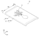
본 발명의 일 실시예로써 스마트 폰에 적용될 수 있는 표시장치(DD)가 도시되었다. 그러나, 이에 한정되지 않고, 본 발명의 일 실시예에 따른 표시장치(DD)는 텔레비전, 퍼스널 컴퓨터, 노트북 컴퓨터, 자동차 네이게이션 유닛, 게임기, 음향 전자장치, 스마트 와치, 카메라 등과 같은 전자장치에 적용될 수 있다. 이것들은 단지 실시예로서 제시된 것들로서, 본 발명의 개념에서 벗어나지 않은 이상 다른 전자장치에도 채용될 수 있음은 물론이다.As an embodiment of the present invention, a display device DD applicable to a smart phone is illustrated. However, the present invention is not limited thereto, and the display device DD according to an embodiment of the present invention can be applied to electronic devices such as a television, a personal computer, a notebook computer, a car navigation unit, a game machine, an acoustic electronic device, a smart watch, a camera, and the like. have. These are only presented as examples, and can be employed in other electronic devices without departing from the concept of the present invention.
도 1a를 참조하면, 표시장치(DD)는 밴딩축(BX)을 기준으로 구분되는 평면영역(NBA) 및 밴딩영역(BA)을 포함할 수 있다. 평면영역(NBA) 제1 표시면(IS1)을 포함하고, 밴딩영역(BA)은 제2 표시면(IS2)을 포함한다.Referring to FIG. 1A, the display device DD may include a planar area NBA and a bending area BA divided based on the bending axis BX. The flat area NBA includes the first display surface IS1, and the bending area BA includes the second display surface IS2.
자세하게, 평면영역(NBA)은 제1 표시면(IS1)의 제1 표시영역(DD-DA1)과 제1 표시영역(DD-DA1)에 인접한 제1 주변영역(DD-NDA1)을 포함할 수 있다. 밴딩영역(BA)은 제2 표시면(IS2)의 제2 표시영역과 제2 표시영역에 인접한 제2 주변영역을 포함할 수 있다. In detail, the flat area NBA may include a first display area DD-DA1 of the first display surface IS1 and a first peripheral area DD-NDA1 adjacent to the first display area DD-DA1. have. The bending area BA may include a second display area of the second display surface IS2 and a second peripheral area adjacent to the second display area.
제1 표시영역(DD-DA1) 및 제2 표시영역(DD-DA2)은 밴딩축(BX)을 기준으로 구분되며, 제1 주변영역(DD-NDA1) 및 제2 주변영역(DD-NDA2)은 밴딩축(BX)을 기준으로 구분된다. 제1 표시영역(DD-DA1) 및 제2 표시영역(DD-DA2)을 통해 이미지(IM)가 표시될 수 있다. The first display area DD-DA1 and the second display area DD-DA2 are divided based on the bending axis BX, and the first peripheral area DD-NDA1 and the second peripheral area DD-NDA2 Are classified based on the bending axis (BX). The image IM may be displayed through the first display area DD-DA1 and the second display area DD-DA2.
또한, 평면 영역(NBA)에서, 이미지(IM)가 표시되는 제1 표시면(IS1)은 제1 방향(DR1)과 제2 방향(DR2)이 정의하는 면과 평행한다. 제1 표시면(IS1)의 법선 방향, 즉 표시장치(DD)의 두께 방향은 제3 방향(DR3)이 지시한다. 각 부재들의 전면(또는 상면)과 배면(또는 하면)은 제3 방향(DR3)에 의해 구분된다. 그러나, 제1 내지 제3 방향들(DR1, DR2, DR3)이 지시하는 방향은 상대적인 개념으로서 다른 방향으로 변환될 수 있다. 이하, 제1 내지 제3 방향들은 제1 내지 제3 방향들(DR1, DR2, DR3)이 각각 지시하는 방향으로 동일한 도면 부호를 참조한다.In addition, in the planar area NBA, the first display surface IS1 on which the image IM is displayed is parallel to a plane defined by the first direction DR1 and the second direction DR2. The third direction DR3 indicates the normal direction of the first display surface IS1, that is, the thickness direction of the display device DD. The front surface (or upper surface) and the rear surface (or lower surface) of each member are divided by a third direction DR3. However, the directions indicated by the first to third directions DR1, DR2, and DR3 are relative concepts and may be converted to other directions. Hereinafter, the first to third directions refer to the same reference numerals as directions indicated by the first to third directions DR1, DR2, and DR3, respectively.
도 1b를 참조하면, 표시장치(DD)는 하나의 평면 영역(NBA) 및 평면 영역(NBA)을 사이에 두고 제1 밴딩영역(BA1) 및 제2 밴딩영역(BA2)을 포함할 수 있다. 제1 밴딩영역(BA1) 및 제2 밴딩영역(BA2)은 제2 방향(DR2)에서 평면 영역(NBA)의 일측 및 타측으로부터 밴딩될 수 있다.Referring to FIG. 1B, the display device DD may include one flat area NBA and a first bending area BA1 and a second bending area BA2 with the flat area NBA interposed therebetween. The first bending area BA1 and the second bending area BA2 may be bent from one side and the other side of the planar area NBA in the second direction DR2.
이하에서, 표시장치(DD)의 설명은 도 1a에 도시된 하나의 밴딩영역(BA)을 갖는 표시장치인 것으로 설명된다. Hereinafter, the description of the display device DD will be described as a display device having one bending area BA shown in FIG. 1A.
도 2는 도 1a에 도시된 표시장치의 단면도이다. 2 is a cross-sectional view of the display device illustrated in FIG. 1A.
도 2를 참조하면, 표시장치(DD)는 보호필름(PM), 표시모듈(DM), 광학부재(LM), 윈도우(WM), 제1 접착부재(AM1), 제2 접착부재(AM2), 및 제3 접착부재(AM3)를 포함한다. 보호필름(PM), 표시모듈(DM), 광학부재(LM), 윈도우(WM), 제1 접착부재(AM1), 제2 접착부재(AM2), 및 제3 접착부재(AM3) 각각은 평면 영역(NBA) 및 밴딩영역(BA)을 포함할 수 있다. Referring to FIG. 2, the display device DD includes a protective film PM, a display module DM, an optical member LM, a window WM, a first adhesive member AM1, and a second adhesive member AM2. , And a third adhesive member AM3. Each of the protective film PM, display module DM, optical member LM, window WM, first adhesive member AM1, second adhesive member AM2, and third adhesive member AM3 is flat It may include an area NBA and a bending area BA.
표시모듈(DM)은 보호필름(PM)과 광학부재(LM) 사이에 배치된다. 광학부재(LM)는 표시모듈(DM)과 윈도우(WM) 사이에 배치된다. 제1 접착부재(AM1)는 표시모듈(DM)과 보호필름(PM)을 결합하고, 제2 접착부재(AM2)는 표시모듈(DM)과 광학부재(LM)를 결합하고, 제3 접착부재(AM3)는 광학부재(LM)와 윈도우(WM)를 결합한다. The display module DM is disposed between the protective film PM and the optical member LM. The optical member LM is disposed between the display module DM and the window WM. The first adhesive member AM1 couples the display module DM and the protective film PM, the second adhesive member AM2 couples the display module DM and the optical member LM, and the third adhesive member AM3 couples the optical member LM and the window WM.
보호필름(PM)은 표시모듈(DM)을 보호한다. 보호필름(PM)은 외부에 노출된 제1 외면(OS-L)을 제공하고, 제1 접착부재(AM1)에 접착되는 접착면을 제공한다. 보호필름(PM)은 외부의 습기가 표시모듈(DM)에 침투하는 것을 방지하고, 외부 충격을 흡수한다.The protective film PM protects the display module DM. The protective film PM provides a first outer surface OS-L exposed to the outside, and provides an adhesive surface adhered to the first adhesive member AM1. The protective film PM prevents external moisture from penetrating into the display module DM and absorbs an external shock.
보호필름(PM)은 플라스틱 필름을 베이스층으로써 포함할 수 있다. 보호필름(PM)은 폴리에테르술폰(PES, polyethersulfone), 폴리아크릴레이트(polyacrylate), 폴리에테르이미드(PEI, polyetherimide), 폴리에틸렌나프탈레이트(PEN, polyethylenenaphthalate), 폴리에틸렌테레프탈레이트(PET, polyethyleneterephthalate), 폴리페닐렌설파이드(PPS, polyphenylene sulfide), 폴리아릴레이트(polyarylate), 폴리이미드(PI, polyimide), 폴리카보네이트(PC, polycarbonate), 폴리아릴렌에테르술폰(poly(arylene ethersulfone)) 및 이들의 조합으로 이루어진 그룹에서 선택된 어느 하나를 포함하는 플라스틱 필름을 포함할 수 있다.The protective film PM may include a plastic film as a base layer. The protective film (PM) is polyethersulfone (PES), polyacrylate, polyetherimide (PEI), polyethylene naphthalate (PEN), polyethylene terephthalate (PET), poly Phenylene sulfide (PPS), polyarylate (polyarylate), polyimide (PI, polyimide), polycarbonate (PC, polycarbonate), polyarylene ethersulfone (poly(arylene ethersulfone)) and combinations thereof It may include a plastic film including any one selected from the group consisting of.
보호필름(PM)을 구성하는 물질은 플라스틱 수지들에 제한되지 않고, 유/무기 복합재료를 포함할 수 있다. 보호필름(PM)은 다공성 유기층 및 유기층의 기공들에 충전된 무기물을 포함할 수 있다. 보호필름(PM)은 플라스틱 필름에 형성된 기능층을 더 포함할 수 있다. 상기 기능층은 수지층을 포함할 수 있다. 상기 기능층은 코팅 방식에 의해 형성될 수 있다. 본 발명의 일 실시예에서 보호필름(PM)은 생략될 수 있다.The material constituting the protective film PM is not limited to plastic resins, and may include an organic/inorganic composite material. The protective film PM may include a porous organic layer and an inorganic material filled in the pores of the organic layer. The protective film PM may further include a functional layer formed on the plastic film. The functional layer may include a resin layer. The functional layer may be formed by a coating method. In an embodiment of the present invention, the protective film PM may be omitted.
윈도우(WM)는 외부 충격으로부터 표시모듈(DM)를 보호하고, 사용자에게 입력면을 제공할 수 있다. 윈도우(WM)는 외부에 노출된 제2 외면(OS-U)을 제공하고, 제3 접착부재(AM3)에 접착되는 접착면을 제공한다. 도 1a 및 도 1b에 도시된 표시면(IS)이 제2 외면(OS-U)일 수 있다.The window WM may protect the display module DM from an external shock and may provide an input surface to a user. The window WM provides a second outer surface OS-U exposed to the outside, and an adhesive surface adhered to the third adhesive member AM3. The display surface IS shown in FIGS. 1A and 1B may be the second outer surface OS-U.
윈도우(WM)는 플라스틱 필름을 포함할 수 있다. 윈도우(WM)는 다층구조를 가질 수 있다. 윈도우(WM)는 유리 기판, 플라스틱 필름, 또는 플라스틱 기판으로부터 선택된 다층구조를 가질 수 있다. 윈도우(WM)는 베젤패턴을 더 포함할 수 있다. 상기 다층구조는 연속공정 또는 접착층을 이용한 접착공정을 통해 형성될 수 있다.The window WM may include a plastic film. The window WM may have a multi-layered structure. The window WM may have a multilayer structure selected from a glass substrate, a plastic film, or a plastic substrate. The window WM may further include a bezel pattern. The multilayer structure may be formed through a continuous process or an adhesion process using an adhesive layer.
광학부재(LM)는 외부광 반사율을 감소시킨다. 광학부재(LM)는 적어도 편광필름을 포함할 수 있다. 광학부재(LM)는 위상차 필름을 더 포함할 수 있다. 한편, 본 발명의 기술적 사상은 이에 한정되지 않으며, 광학부재(LM)는 생략될 수도 있다.The optical member LM reduces reflectance of external light. The optical member LM may include at least a polarizing film. The optical member LM may further include a retardation film. Meanwhile, the technical idea of the present invention is not limited thereto, and the optical member LM may be omitted.
표시모듈(DM)은 유기발광 표시패널(DP) 및 터치감지유닛(TS)을 포함할 수 있다. 터치감지유닛(TS)은 유기발광 표시패널(DP) 상에 직접 배치된다. 본 명세서에서 "직접 배치된다"는 것은 별도의 접착층을 이용하여 부착하는 것을 제외하며, 연속공정에 의해 형성된 것을 의미한다.The display module DM may include an organic light emitting display panel DP and a touch sensing unit TS. The touch sensing unit TS is directly disposed on the organic light emitting display panel DP. In the present specification, "directly arranged" means that it is formed by a continuous process, excluding attachment using a separate adhesive layer.
유기발광 표시패널(DP)은 입력된 영상 데이터에 대응하는 이미지(IM, 도 1a 참조)를 생성한다. 유기발광 표시패널(DP)은 두께 방향(DR3)에서 마주하는 제1 표시 패널면(BS1-L) 및 제2 표시 패널면(BS1-U)을 제공한다. 본 실시예에서 유기발광 표시패널(DP)을 예시적으로 설명하였으나, 표시패널은 이에 제한되지 않는다.The organic light-emitting display panel DP generates an image (IM, see FIG. 1A) corresponding to the input image data. The organic light emitting display panel DP provides a first display panel surface BS1-L and a second display panel surface BS1-U facing in the thickness direction DR3. In the present embodiment, the organic light emitting display panel DP has been described as an example, but the display panel is not limited thereto.
터치감지유닛(TS)은 외부입력의 좌표정보를 획득한다. 터치감지유닛(TS)은 정전용량 방식으로 외부입력을 감지할 수 있다.The touch sensing unit TS acquires coordinate information of an external input. The touch sensing unit TS may detect an external input using a capacitive method.
별도로 도시하지 않았으나, 본 발명의 일 실시예에 따른 표시모듈(DM)은 반사 방지층을 더 포함할 수도 있다. 반사 방지층은 컬러필터 또는 도전층, 절연층, 및 도전층의 적층 구조물을 포함할 수 있다. 반사 방지층은 외부로부터 입사된 광을 흡수 또는 상쇄간섭 또는 편광시켜 외부광 반사율을 감소시킬 수 있다. 반사 방지층은 광학 부재(LM)의 기능을 대체할 수 있다.Although not shown separately, the display module DM according to an embodiment of the present invention may further include an antireflection layer. The antireflection layer may include a color filter or a layered structure of a conductive layer, an insulating layer, and a conductive layer. The antireflection layer may reduce external light reflectance by absorbing, destructive interference, or polarizing light incident from the outside. The antireflection layer may replace the function of the optical member LM.
제1 접착 부재(AM1), 제2 접착 부재(AM2), 및 제3 접착 부재(AM3) 각각은 광학 투명 접착 필름(OCA, Optically Clear Adhesive film) 또는 광학 투명 접착 수지(OCR, Optically Clear Resin) 또는 감압 접착 필름(PSA, Pressure Sensitive Adhesive film)과 같은 유기 접착층일 수 있다. 유기 접착층은 폴리우레탄계, 폴리아크릴계, 폴리에스테르계, 폴리에폭시계, 폴리초산비닐계 등의 접착물질을 포함할 수 있다. 결과적으로 유기 접착층은 유기층의 하나에 해당한다. 후술하는 것과 같이 유기 접착층은 기포 발생의 원인이 될 수 있다.Each of the first adhesive member AM1, the second adhesive member AM2, and the third adhesive member AM3 is an optically clear adhesive film (OCA) or an optically clear adhesive resin (OCR) Alternatively, it may be an organic adhesive layer such as a pressure sensitive adhesive film (PSA). The organic adhesive layer may include an adhesive material such as polyurethane-based, polyacrylic-based, polyester-based, polyepoxy clock, and polyvinyl acetate-based. As a result, the organic adhesive layer corresponds to one of the organic layers. As will be described later, the organic adhesive layer may cause bubbles.
별도로 도시하지 않았으나, 표시장치(DD)는 도 1a 및 도 1b에 도시된 상태를 유지하기 위해 상기 기능층들을 지지하는 프레임 구조물을 더 포함할 수 있다. 프레임 구조물은 관절 구조 또는 힌지 구조를 포함할 수 있다. Although not shown separately, the display device DD may further include a frame structure supporting the functional layers to maintain the state shown in FIGS. 1A and 1B. The frame structure may include an articulated structure or a hinge structure.
도 3a는 본 발명의 실시 예에 따른 표시패널의 평면도이다. 도 3b는 본 발명의 실시 예에 따른 표시모듈의 단면도이다. 3A is a plan view of a display panel according to an exemplary embodiment of the present invention. 3B is a cross-sectional view of a display module according to an embodiment of the present invention.
도 3a를 참조하면, 유기발광 표시패널(DP)은 평면상에서 표시영역(DA)과 주변영역(NDA)을 포함한다. 유기발광 표시패널(DP)의 표시영역(DA) 및 주변영역(NDA)은 표시장치(DD)의 표시영역(DD-DA) 및 주변영역(DD-NDA)에 각각 대응한다. 유기발광 표시패널(DP)의 표시영역(DA) 및 주변영역(NDA)은 표시장치(DD)의 표시영역(DD-DA) 및 주변영역(DD-NDA)과 반드시 동일할 필요는 없고, 유기발광 표시패널(DP)의 구조/디자인에 따라 변경될 수 있다.Referring to FIG. 3A, the organic light emitting display panel DP includes a display area DA and a peripheral area NDA on a plane. The display area DA and the peripheral area NDA of the organic light emitting display panel DP correspond to the display area DD-DA and the peripheral area DD-NDA of the display device DD, respectively. The display area DA and the peripheral area NDA of the organic light emitting display panel DP do not necessarily have to be the same as the display area DD-DA and the peripheral area DD-NDA of the display device DD. It may be changed according to the structure/design of the light emitting display panel DP.
유기발광 표시패널(DP)은 복수 개의 게이트 라인들(GL), 복수 개의 데이터 라인들(DL), 복수 개의 발광 라인들(EL), 복수개의 제1 및 제2 초기화 라인들(SL-Vint1, SL-Vint2), 복수 개의 제1 전원 라인들(SL-VDD1, SL-VDD2), 제2 전원 라인(E-VSS), 복수 개의 패드부들(PD), 복수 개의 신호 연결 라인들(SCL), 게이트-발광 구동부(GDC), 및 복수 개의 화소들(PX)을 포함한다.The organic light emitting display panel DP includes a plurality of gate lines GL, a plurality of data lines DL, a plurality of emission lines EL, a plurality of first and second initialization lines SL-Vint1, SL-Vint2), a plurality of first power lines SL-VDD1 and SL-VDD2, a second power line E-VSS, a plurality of pad portions PD, a plurality of signal connection lines SCL, A gate-emitting driver GDC and a plurality of pixels PX are included.
화소들(PX)이 배치된 영역이 표시영역(DA)으로 정의된다. 본 실시예에서 주변영역(NDA)은 표시영역(DA)의 테두리를 따라 정의될 수 있다. The area where the pixels PX are disposed is defined as the display area DA. In this embodiment, the peripheral area NDA may be defined along the edge of the display area DA.
게이트 라인들(GL)은 제2 방향(DR2)으로 연장되어 복수 개의 화소들(PX) 중 대응하는 화소(PX)에 각각 연결되고, 데이터 라인들(DL)은 제1 방향(DR1)으로 연장되어 복수 개의 화소들 중 대응하는 화소(PX)에 각각 연결되고, 발광 라인들(EL)은 제2 방향(DR2)으로 연장되어 복수 개의 화소들 중 대응하는 화소(PX)에 각각 연결된다.The gate lines GL extend in the second direction DR2 and are respectively connected to a corresponding pixel PX among the plurality of pixels PX, and the data lines DL extend in the first direction DR1. Thus, each of the plurality of pixels is connected to a corresponding pixel PX, and the emission lines EL extend in the second direction DR2 and are respectively connected to a corresponding pixel PX among the plurality of pixels.
제1 전원 라인들(SL-VDD1, SL-VDD2)은 제1 방향(DR1)으로 연장된 복수 개의 제1 서브 전원 라인들(SL-VDD1) 및 제2 방향(DR2)으로 연장되어 제1 서브 전원 라인들(SL-VDD1)에 연결된 복수 개의 제2 전원 라인들(SL-VDD2)을 포함한다. 제2 전원 라인들(SL-VDD2)은 화소들(PX)에 연결되며, 제1 및 제2 전원 라인들(SL-VDD1, SL-VDD2)은 제1 전압을 수신한다. 제1 전압은 애노드 전압으로 정의될 수 있다.The first power lines SL-VDD1 and SL-VDD2 are a plurality of first sub power lines SL-VDD1 extending in a first direction DR1 and a first sub power line SL-VDD1 extending in a second direction DR2. It includes a plurality of second power lines SL-VDD2 connected to the power lines SL-VDD1. The second power lines SL-VDD2 are connected to the pixels PX, and the first and second power lines SL-VDD1 and SL-VDD2 receive a first voltage. The first voltage may be defined as the anode voltage.
제1 초기화 라인들(SL-Vint1)은 제1 방향(DR1)으로 연장되고, 제2 초기화 라인들(SL-Vint2)은 제2 방향(DR2)으로 연장되어 제1 초기화 라인들(SL-Vint1)에 연결된다. 제1 초기화 라인들(SL-Vint1)은 화소들(PX)에 연결되며, 초기화 전압을 수신한다.The first initialization lines SL-Vint1 extend in the first direction DR1, and the second initialization lines SL-Vint2 extend in the second direction DR2, and the first initialization lines SL-Vint1 ). The first initialization lines SL-Vint1 are connected to the pixels PX and receive an initialization voltage.
게이트-발광 구동부(GDC)는 주변영역(NDA)의 일측에 배치되며, 게이트 라인들(GL) 및 발광 라인들(EL)에 연결된다. 게이트-발광 구동부(GDC)는 신호 연결 라인들(SCL) 중 대응하는 제1 신호 연결 라인을 통해 제어 신호를 수신하고, 수신된 제어 신호에 응답하여 게이트 신호들 및 발광 신호들을 생성할 수 있다. 제1 신호 연결 라인의 일단은 게이트-발광 구동부(GDC)에 연결되며, 끝단은 패드부들(PD)에 연결된다. 게이트 라인들(GL)은 게이트 신호들을 수신하고, 발광 라인들(EL)은 발광 신호들을 수신한다. 도 3a에 도시된 게이트-발광 구동부(GDC)와 제2 방향(DR2)에서 마주하는 또 다른 게이트-발광 구동부가 더 배치될 수 있다. The gate-emission driver GDC is disposed on one side of the peripheral area NDA, and is connected to the gate lines GL and the emission lines EL. The gate-emission driver GDC may receive a control signal through a corresponding first signal connection line among the signal connection lines SCL, and generate gate signals and light emission signals in response to the received control signal. One end of the first signal connection line is connected to the gate-light-emitting driver GDC, and an end of the first signal connection line is connected to the pad parts PD. The gate lines GL receive gate signals, and the emission lines EL receive emission signals. Another gate-emission driver that faces the gate-emission driver GDC shown in FIG. 3A and the second direction DR2 may be further disposed.
제2 전원 라인(E-VSS)은 제2 전압을 수신하며, 제2 전압은 캐소드 전압(또는 접지 전압)으로 정의될 수 있다. 도시하지 않았으나, 제2 전원 라인(E-VSS)을 통해 제2 전압이 화소들(PX)에 제공될 수 있다. 제2 전원 라인(E-VSS)은 신호 연결 라인들(SCL) 중 대응하는 제2 신호 연결 라인을 통해 제어 신호를 수신한다. 제2 신호 연결 라인의 일단은 제2 전원 라인(E-VSS)에 연결되고, 끝단은 패드부들(PD)에 연결된다.The second power line E-VSS receives a second voltage, and the second voltage may be defined as a cathode voltage (or a ground voltage). Although not shown, a second voltage may be provided to the pixels PX through the second power line E-VSS. The second power line E-VSS receives a control signal through a corresponding second signal connection line among the signal connection lines SCL. One end of the second signal connection line is connected to the second power line E-VSS, and an end of the second signal connection line is connected to the pad portions PD.
도 3b를 참조하면, 유기발광 표시패널(DP)은 베이스층(SUB), 베이스층(SUB) 상에 배치된 회로층(DP-CL), 발광소자층(DP-OLED), 및 박막 봉지층(TFE)을 포함한다. 베이스층(SUB)은 적어도 하나의 플라스틱 필름을 포함할 수 있다. 베이스층(SUB)은 플렉서블한 기판으로 플라스틱 기판, 유리 기판, 메탈 기판, 또는 유/무기 복합재료 기판 등을 포함할 수 있다. Referring to FIG. 3B, the organic light emitting display panel DP includes a base layer SUB, a circuit layer DP-CL disposed on the base layer SUB, a light emitting device layer DP-OLED, and a thin film encapsulation layer. (TFE). The base layer SUB may include at least one plastic film. The base layer SUB is a flexible substrate and may include a plastic substrate, a glass substrate, a metal substrate, or an organic/inorganic composite material substrate.
회로층(DP-CL)은 복수 개의 절연층들, 복수 개의 도전층들 및 반도체층을 포함할 수 있다. 회로층(DP-CL)의 복수 개의 도전층들은 신호라인들 또는 화소의 제어회로를 구성할 수 있다. 발광소자층(DP-OLED)은 유기발광 다이오드들을 포함한다. 박막 봉지층(TFE)은 발광소자층(DP-OLED)을 밀봉한다. 박막 봉지층(TFE)은 무기층과 유기층을 포함한다. 박막 봉지층(TFE)은 적어도 2 개의 무기층들과 그 사이에 배치된 유기층을 포함할 수 있다. 무기층들은 수분/산소로부터 발광소자층(DP-OLED)을 보호하고, 유기층은 먼지 입자와 같은 이물질로부터 발광소자층(DP-OLED)을 보호한다. 무기층은 실리콘 나이트라이드층, 실리콘 옥시 나이트라이드층 및 실리콘 옥사이드층, 티타늄옥사이드층, 또는 알루미늄옥사이드층 등을 포함할 수 있다. 유기층은 아크릴 계열 유기층을 포함할 수 있고, 이에 제한되지 않는다.The circuit layer DP-CL may include a plurality of insulating layers, a plurality of conductive layers, and a semiconductor layer. The plurality of conductive layers of the circuit layer DP-CL may constitute signal lines or a control circuit of a pixel. The light emitting device layer DP-OLED includes organic light emitting diodes. The thin film encapsulation layer TFE seals the light emitting device layer DP-OLED. The thin film encapsulation layer (TFE) includes an inorganic layer and an organic layer. The thin film encapsulation layer TFE may include at least two inorganic layers and an organic layer disposed therebetween. The inorganic layers protect the light emitting device layer (DP-OLED) from moisture/oxygen, and the organic layer protects the light emitting device layer (DP-OLED) from foreign substances such as dust particles. The inorganic layer may include a silicon nitride layer, a silicon oxy nitride layer and a silicon oxide layer, a titanium oxide layer, or an aluminum oxide layer. The organic layer may include an acrylic organic layer, but is not limited thereto.
터치감지유닛(TS)은 박막 봉지층(TFE) 상에 직접 배치된다. 터치감지유닛(TS)은 터치센서들과 터치 신호라인들을 포함한다. 터치센서들과 터치 신호라인들은 단층 또는 다층구조를 가질 수 있다. The touch sensing unit TS is directly disposed on the thin film encapsulation layer TFE. The touch sensing unit TS includes touch sensors and touch signal lines. The touch sensors and the touch signal lines may have a single layer or a multilayer structure.
터치센서들과 터치 신호라인들은 ITO(indium tin oxide), IZO(indium zinc oxide), ZnO(zinc oxide), ITZO(indium tin zinc oxide), PEDOT, 금속 나노 와이어, 그라핀을 포함할 수 있다. 터치센서들과 터치 신호라인들은 금속층, 예컨대 몰리브덴, 은, 티타늄, 구리, 알루미늄, 또는 이들의 합금을 포함할 수 있다. 터치센서들과 터치 신호라인들은 동일한 층구조를 갖거나, 다른 층구조를 가질 수 있다. 터치감지유닛(TS)에 대한 구체적인 내용은 후술한다.The touch sensors and touch signal lines may include indium tin oxide (ITO), indium zinc oxide (IZO), zinc oxide (ZnO), indium tin zinc oxide (ITZO), PEDOT, metal nanowires, and graphene. The touch sensors and the touch signal lines may include a metal layer, such as molybdenum, silver, titanium, copper, aluminum, or an alloy thereof. The touch sensors and the touch signal lines may have the same layer structure or may have different layer structures. Details of the touch sensing unit TS will be described later.
도 4a는 본 발명의 실시 예에 따른 화소의 등가회로도이다. 도 4b 및 도 4c는 본 발명의 실시 예에 따른 표시패널의 부분 단면도이다. 4A is an equivalent circuit diagram of a pixel according to an exemplary embodiment of the present invention. 4B and 4C are partial cross-sectional views of a display panel according to an exemplary embodiment of the present invention.
도 4a에는 데이터 라인들(DL) 중 k번째 데이터 라인(DLk)에 연결된 i번째 화소(PXi)가 예시적으로 도시되었다. 도 4b는 도 4a에 도시된 등가회로의 제1 트랜지스터(T1)에 대응하는 부분의 단면을 도시하였다. 도 4c는 도 4a에 도시된 등가회로의 제2 트랜지스터(T2), 제6 트랜지스터(T6) 및 유기발광 다이오드(OLED)에 대응하는 부분의 단면을 도시하였다. In FIG. 4A, an i-th pixel PXi connected to the k-th data line DLk among the data lines DL is illustrated as an example. 4B is a cross-sectional view of a portion of the equivalent circuit shown in FIG. 4A corresponding to the first transistor T1. 4C is a cross-sectional view of a portion corresponding to the second transistor T2, the sixth transistor T6 and the organic light emitting diode OLED of the equivalent circuit shown in FIG. 4A.
도 4a를 참조하면, i번째 화소(PXi)는 유기발광 다이오드(OLED) 및 유기발광 다이오드를 제어하는 화소 구동회로를 포함한다. 구동회로는 7개의 박막 트랜지스터들(T1~T7) 및 하나의 커패시터(Cst)를 포함할 수 있다. 한편, 7개의 박막 트랜지스터들(T1~T7) 및 하나의 커패시터(Cst)를 포함하는 화소 구동회로를 예시적으로 도시하였으나, 화소(PXi)는 유기발광 다이오드(OLED)를 구동하기 위한 구동회로로써 제1 트랜지스터(T1, 또는 구동 트랜지스터), 제2 트랜지스터(T2, 또는 스위칭 트랜지스터), 및 커패시터(Cst)를 포함하면 충분하고, 화소 구동회로는 다양하게 변형될 수 있다.Referring to FIG. 4A, an i-th pixel PXi includes an organic light emitting diode OLED and a pixel driving circuit that controls the organic light emitting diode. The driving circuit may include seven thin film transistors T1 to T7 and one capacitor Cst. Meanwhile, a pixel driving circuit including seven thin film transistors T1 to T7 and one capacitor Cst is illustrated as an example, but the pixel PXi is a driving circuit for driving the organic light emitting diode OLED. It is sufficient to include the first transistor T1 or the driving transistor, the second transistor T2 or the switching transistor, and the capacitor Cst, and the pixel driving circuit may be variously modified.
구동 트랜지스터는 유기발광 다이오드(OLED)에 공급되는 구동전류를 제어한다. 제2 트랜지스터(T2)의 출력전극은 유기발광 다이오드(OLED)와 전기적으로 연결된다. 제2 트랜지스터(T2)의 출력전극은 유기발광 다이오드(OLED)의 애노드와 직접 접촉하거나, 다른 트랜지스터, 일 예로 제6 트랜지스터(T6)를 경유하여 연결될 수 있다.The driving transistor controls the driving current supplied to the organic light emitting diode (OLED). The output electrode of the second transistor T2 is electrically connected to the organic light emitting diode OLED. The output electrode of the second transistor T2 may directly contact the anode of the organic light emitting diode OLED, or may be connected via another transistor, for example, the sixth transistor T6.
제어 트랜지스터의 제어 전극은 제어 신호를 수신할 수 있다. i번째 화소(PXi)에 인가되는 제어 신호는 i-1번째 게이트 신호(Si-1), i번째 게이트 신호(Si), i+1번째 게이트 신호(Si+1), 데이터 신호(Di), 및 i번째 발광 제어 신호(Ei)를 포함할 수 있다. 본 발명의 실시예에서 제어 트랜지스터는 제1 트랜지스터(T1) 및 제3 내지 제7 트랜지스터들(T3~T7)을 포함할 수 있다. The control electrode of the control transistor may receive a control signal. The control signals applied to the i-th pixel PXi include the i-1th gate signal Si-1, the i-th gate signal Si, the i+1th gate signal Si+1, the data signal Di, and And an i-th emission control signal Ei. In an embodiment of the present invention, the control transistor may include a first transistor T1 and third to seventh transistors T3 to T7.
제1 트랜지스터(T1)는 k번째 데이터 라인(DLk)에 접속된 입력 전극, i번째 게이트 라인(SLi)에 접속된 제어 전극, 및 제2 트랜지스터(T2)의 출력 전극에 접속된 출력 전극을 포함한다. 제1 트랜지스터(T1)는 i번째 게이트 라인(SLi)에 인가된 게이트 신호(Si, 이하 i번째 게이트 신호)에 의해 턴-온되고, k번째 데이터 라인(DLk)에 인가된 데이터 신호(Dk)를 스토리지 커패시터(Cst)에 제공한다. The first transistor T1 includes an input electrode connected to the k-th data line DLk, a control electrode connected to the i-th gate line SLi, and an output electrode connected to the output electrode of the second transistor T2. do. The first transistor T1 is turned on by a gate signal Si applied to the i-th gate line SLi (hereinafter, i-th gate signal), and the data signal Dk applied to the k-th data line DLk Is provided to the storage capacitor Cst.
도 4b 및 도 4c를 참조하면, 베이스 기판(SUB) 상에 제1 트랜지스터(T1), 제2 트랜지스터(T2) 및 제6 트랜지스터(T6)가 배치된다. 트랜지스터들의 구조는 실질적으로 동일하므로, 이하 제1 트랜지스터(T1)의 구성이 설명되고, 제2 및 제6 트랜지스터들(T2, T6)의 구성에 대한 설명은 생략될 것이다. 4B and 4C, a first transistor T1, a second transistor T2, and a sixth transistor T6 are disposed on the base substrate SUB. Since the structures of the transistors are substantially the same, a configuration of the first transistor T1 will be described below, and a description of the configurations of the second and sixth transistors T2 and T6 will be omitted.
베이스 기판(SUB)의 상면은 제1 방향(DR1) 및 제2 방향(DR2)으로 정의된다. 제1 트랜지스터(T1)는 제1 입력 전극(DE1), 제1 출력 전극(SE1), 제1 제어 전극(GE1), 및 제1 산화물 반도체 패턴(OSP1)을 포함한다. The top surface of the base substrate SUB is defined in a first direction DR1 and a second direction DR2. The first transistor T1 includes a first input electrode DE1, a first output electrode SE1, a first control electrode GE1, and a first oxide semiconductor pattern OSP1.
베이스 기판(SUB)의 상면에 버퍼층(BFL)이 배치될 수 있다. 버퍼층(BFL)은 베이스 기판(SUB)과 도전성 패턴들 또는 반도체 패턴들의 결합력을 향상시킨다. 버퍼층(BFL)은 무기층을 포함할 수 있다. 별도로 도시되지 않았으나, 이물질이 유입되는 것을 방지하는 배리어층이 베이스 기판(SUB)의 상면에 더 배치될 수도 있다. 버퍼층(BFL)과 배리어층은 선택적으로 배치 또는 생략될 수 있다. The buffer layer BFL may be disposed on the upper surface of the base substrate SUB. The buffer layer BFL improves bonding strength between the base substrate SUB and the conductive patterns or semiconductor patterns. The buffer layer BFL may include an inorganic layer. Although not shown separately, a barrier layer that prevents foreign substances from entering may be further disposed on the upper surface of the base substrate SUB. The buffer layer BFL and the barrier layer may be selectively disposed or omitted.
베이스 기판(SUB)은 플라스틱 기판, 유리 기판, 금속 기판 등을 포함할 수 있다. 플라스틱 기판은 아크릴계 수지, 메타크릴계 수지, 폴리이소프렌, 비닐계 수지, 에폭시계 수지, 우레탄계 수지, 셀룰로오스계 수지, 실록산계 수지, 폴리이미드계 수지, 폴리아미드계 수지 및 페릴렌계 수지 중 적어도 어느 하나를 포함할 수 있다. The base substrate SUB may include a plastic substrate, a glass substrate, a metal substrate, or the like. The plastic substrate is at least one of acrylic resin, methacrylic resin, polyisoprene, vinyl resin, epoxy resin, urethane resin, cellulose resin, siloxane resin, polyimide resin, polyamide resin, and perylene resin It may include.
버퍼층(BFL) 상에 제1 산화물 반도체 패턴(OSP1)이 배치된다. 제1 산화물 반도체 패턴(OSP1)은 인듐-주석 산화물(ITO), 인듐-갈륨-아연 산화물(IGZO), 아연 산화물(ZnO), 인듐-아연 산화물(IZnO) 등을 포함할 수 있다.The first oxide semiconductor pattern OSP1 is disposed on the buffer layer BFL. The first oxide semiconductor pattern OSP1 may include indium-tin oxide (ITO), indium-gallium-zinc oxide (IGZO), zinc oxide (ZnO), indium-zinc oxide (IZnO), and the like.
버퍼층(BFL) 상에 제1 산화물 반도체 패턴(OSP1)을 커버하는 제1 절연층(10)이 배치된다. The first insulating
제1 절연층(10) 상에 제1 제어 전극(GE1)이 배치되고, 제1 절연층(10) 상에 제1 제어 전극(GE1)을 커버하는 제2 절연층(20)이 배치된다. 제2 절연층(20)은 평탄한 상면을 제공할 수 있다. 제2 절연층(20)은 유기 물질 및/또는 무기 물질을 포함할 수 있다. A first control electrode GE1 is disposed on the first insulating
제1 절연층(10) 및 제2 절연층(20)은 무기 물질을 포함할 수 있다. 무기 물질은 알루미늄 옥사이드, 티타늄 옥사이드, 실리콘 옥사이드, 실리콘옥시나이트라이드, 지르코늄옥사이드, 및 하프늄 옥사이드 중 적어도 하나를 포함할 수 있다. The first insulating
한편, 제1 산화물 반도체 패턴(OSP1)의 제1 영역과 제2 영역을 노출시키는 제1 컨택홀(CH1) 및 제2 컨택홀(CH2)이 제1 및 제2 절연층들(10, 20)에 정의된다. 제1 컨택홀(CH1) 및 제2 컨택홀(CH2) 각각은 제1 절연층(10)과 제2 절연층(20)을 관통한다.Meanwhile, the first contact hole CH1 and the second contact hole CH2 exposing the first and second regions of the first oxide semiconductor pattern OSP1 are formed of the first and second insulating
제1 입력 전극(DE1)과 제1 출력 전극(SE1)은 제2 절연층(20) 상에 배치된다. 제1 입력 전극(DE1)과 제1 출력 전극(SE1)은 제1 컨택홀(CH1) 및 제2 컨택홀(CH2)을 통해 제1 산화물 반도체 패턴(OSP1)의 제1 영역과 제2 영역에 각각 접속된다.The first input electrode DE1 and the first output electrode SE1 are disposed on the second insulating
제2 절연층(20) 상에 제1 입력 전극(DE1)과 제1 출력 전극(SE1)을 커버하는 제3 절연층(30)이 배치된다. 제3 절연층(30)은 평탄한 상면을 제공할 수 있다. 제3 절연층(30)은 유기 물질 및/또는 무기 물질을 포함할 수 있다. 즉, 제3 절연층(30)은 입력 전극들 및 출력 전극들을 커버할 수 있다. A third insulating
도 4c는 제2 트랜지스터(T2)와 실질적으로 동일한 구조의 제6 트랜지스터(T6)를 예시적으로 도시하였다. 그러나, 제6 트랜지스터(T6)의 구조는 변형될 수 있다. 제6 트랜지스터(T6)의 입력 전극(DE6)은 제3 절연층(30) 상에서 제2 트랜지스터(T2)의 출력 전극(SE2)에 연결된다.FIG. 4C exemplarily illustrates a sixth transistor T6 having substantially the same structure as the second transistor T2. However, the structure of the sixth transistor T6 may be modified. The input electrode DE6 of the sixth transistor T6 is connected to the output electrode SE2 of the second transistor T2 on the third insulating
제3 절연층(30) 상에 화소정의막(PDL) 및 유기발광 다이오드(OLED)가 배치된다. 제3 절연층(30) 상에 애노드(AE)가 배치된다. 애노드(AE)는 제3 절연층(30)을 관통하는 제7 컨택홀(CH7)을 통해 제6 트랜지스터(T6)의 제6 출력 전극(SE6)에 연결된다. 화소정의막(PDL)에는 개구부(OP)가 정의된다. 화소정의막(PDL)의 개구부(OP)는 애노드(AE)의 적어도 일부분을 노출시킨다. A pixel defining layer PDL and an organic light emitting diode OLED are disposed on the third insulating
화소(PX)는 유기발광 표시패널(DP)의 평면상에서 화소 영역에 배치될 수 있다. 화소 영역은 발광영역(PXA)과 발광영역(PXA)에 인접한 비발광영역(NPXA)을 포함할 수 있다. 비발광영역(NPXA)은 발광영역(PXA)을 둘러싸도록 배치될 수 있다. 본 실시예에서 발광영역(PXA)은 애노드(AE)에 대응하게 정의되었다. 그러나, 발광영역(PXA)은 이에 제한되지 않고, 발광영역(PXA)은 광이 발생되는 영역으로 정의되면 충분하다. 발광영역(PXA)은 개구부(OP)에 의해 노출된 애노드(AE)의 일부영역에 대응하게 정의될 수도 있다.The pixel PX may be disposed in a pixel area on the plane of the organic light emitting display panel DP. The pixel area may include an emission area PXA and a non-emission area NPXA adjacent to the emission area PXA. The non-emission area NPXA may be disposed to surround the emission area PXA. In this embodiment, the light-emitting area PXA is defined to correspond to the anode AE. However, the emission area PXA is not limited thereto, and it is sufficient if the emission area PXA is defined as an area where light is generated. The emission area PXA may be defined to correspond to a partial area of the anode AE exposed by the opening OP.
정공 제어층(HCL)은 발광영역(PXA)과 비발광영역(NPXA)에 공통으로 배치될 수 있다. 별도로 도시되지 않았으나, 정공 제어층(HCL)과 같은 공통층은 복수 개의 화소들(PX)에 공통으로 형성될 수 있다.The hole control layer HCL may be commonly disposed in the light-emitting area PXA and the non-emissive area NPXA. Although not shown separately, a common layer such as the hole control layer HCL may be formed in common with the plurality of pixels PX.
정공 제어층(HCL) 상에 유기발광층(EML)이 배치된다. 유기발광층(EML)은 개구부(OP)에 대응하는 영역에만 배치될 수 있다. 즉, 유기발광층(EML)은 복수 개의 화소들(PX) 각각에 분리되어 형성될 수 있다. An organic light emitting layer EML is disposed on the hole control layer HCL. The organic emission layer EML may be disposed only in a region corresponding to the opening OP. That is, the organic emission layer EML may be formed separately on each of the plurality of pixels PX.
유기발광층(EML) 상에 전자 제어층(ECL)이 배치된다. 전자 제어층(ECL) 상에 캐소드(CE)가 배치된다. 캐소드(CE)는 복수 개의 화소들(PX)에 공통적으로 배치된다. An electron control layer ECL is disposed on the organic emission layer EML. The cathode CE is disposed on the electron control layer ECL. The cathode CE is commonly disposed on the plurality of pixels PX.
캐소드(CE) 상에 박막 봉지층(TFE)이 배치된다. 박막 봉지층(TFE)은 복수 개의 화소들(PX)에 공통적으로 배치된다. 박막 봉지층(TFE)은 적어도 하나의 무기층과 적어도 하나의 유기층을 포함한다. 박막 봉지층(TFE)은 교번하게 적층된 복수 개의 무기층들과 복수 개의 유기층들을 포함할 수 있다.A thin film encapsulation layer TFE is disposed on the cathode CE. The thin film encapsulation layer TFE is commonly disposed on the plurality of pixels PX. The thin film encapsulation layer TFE includes at least one inorganic layer and at least one organic layer. The thin film encapsulation layer TFE may include a plurality of inorganic layers and a plurality of organic layers alternately stacked.
본 실시예에서 패터닝된 유기발광층(EML)을 예시적으로 도시하였으나, 유기발광층(EML)은 복수 개의 화소들(PX)에 공통적으로 배치될 수 있다. 이때, 유기발광층(EML)은 백색 광을 생성할 수 있다. 또한, 유기발광층(EML)은 다층구조를 가질 수 있다.In the present embodiment, the patterned organic emission layer EML is illustrated as an example, but the organic emission layer EML may be commonly disposed on the plurality of pixels PX. In this case, the organic light emitting layer EML may generate white light. In addition, the organic light emitting layer EML may have a multilayer structure.
본 실시예에서 박막 봉지층(TFE)은 캐소드(CE)를 직접 커버한다. 본 발명의 일 실시예에서, 캐소드(CE)를 커버하는 캡핑층이 더 배치될 수 있다. 이때 박막 봉지층(TFE)은 캡핑층을 직접 커버할 수 있다.In this embodiment, the thin film encapsulation layer TFE directly covers the cathode CE. In an embodiment of the present invention, a capping layer covering the cathode CE may be further disposed. In this case, the thin film encapsulation layer (TFE) may directly cover the capping layer.
도 5a 내지 도 5c는 본 발명의 실시 예에 따른 박막 봉지층의 단면도들이다. 5A to 5C are cross-sectional views of a thin film encapsulation layer according to an embodiment of the present invention.
도 5a 내지 도 5c를 참조하여 본 발명의 실시 예들에 따른 박막 봉지층들(TFE1, TFE2, TFE3)을 설명한다.Thin film encapsulation layers TFE1, TFE2, and TFE3 according to embodiments of the present invention will be described with reference to FIGS. 5A to 5C.
먼저, 도 5a에 도시된 것과 같이, 박막 봉지층(TFE1)은 n개의 무기층들(IOL1 내지 IOLn)을 포함할 수 있다. 박막 봉지층(TFE1)은 n-1개의 유기층들(OL1 내지 OLn-1)을 포함하고, n-1개의 유기층들(OL1 내지 OLn-1)은 n개의 무기층들(IOL1 내지 IOLn)과 교번하게 배치될 수 있다. n-1개의 유기층들(OL1 내지 OLn-1)은 평균적으로 n개의 무기층들(IOL1 내지 IOLn)보다 더 큰 두께를 가질 수 있다.First, as shown in FIG. 5A, the thin film encapsulation layer TFE1 may include n inorganic layers IOL1 to IOLn. The thin film encapsulation layer TFE1 includes n-1 organic layers OL1 to OLn-1, and n-1 organic layers OL1 to OLn-1 alternate with n inorganic layers IOL1 to IOLn. Can be arranged. The n-1 organic layers OL1 to OLn-1 may have a thickness greater than that of the n inorganic layers IOL1 to IOLn on average.
n개의 무기층들(IOL1 내지 IOLn) 각각은 1개의 물질을 포함하는 단층이거나, 각각이 다른 물질을 포함하는 복층을 가질 수 있다. n-1개의 유기층들(OL1 내지 OLn-1) 각각은 유기 모노머들을 증착 또는 프린팅 또는 코팅하여 형성될 수 있다. 유기 모노머들은 아크릴계 모노머를 포함할 수 있다. Each of the n inorganic layers IOL1 to IOLn may have a single layer including one material or a multilayer including a different material. Each of the n-1 organic layers OL1 to OLn-1 may be formed by depositing, printing, or coating organic monomers. Organic monomers may include acrylic monomers.
도 5b 및 도 5c에 도시된 것과 같이, 박막 봉지층들(TFE2, TFE3) 각각에 포함된 무기층들은 서로 동일하거나 다른 무기물질을 가질 수 있고, 서로 동일하거나 다른 두께를 가질 수 있다. 박막 봉지층들(TFE2, TFE3) 각각에 포함된 유기층들은 서로 동일하거나 다른 유기물질을 가질 수 있고, 서로 동일하거나 다른 두께를 가질 수 있다.As shown in FIGS. 5B and 5C, the inorganic layers included in each of the thin film encapsulation layers TFE2 and TFE3 may have the same or different inorganic material, and may have the same or different thickness. The organic layers included in each of the thin film encapsulation layers TFE2 and TFE3 may have the same or different organic materials, and may have the same or different thickness.
도 5b에 도시된 것과 같이, 박막 봉지층(TFE2)은 순차적으로 적층된 제1 무기층(IOL1), 제1 유기층(OL1), 제2 무기층(IOL2), 제2 유기층(OL2), 및 제3 무기층(IOL3)을 포함할 수 있다. As shown in FIG. 5B, the thin film encapsulation layer TFE2 includes a first inorganic layer IOL1, a first organic layer OL1, a second inorganic layer IOL2, a second organic layer OL2, and It may include a third inorganic layer (IOL3).
제1 무기층(IOL1)은 2층 구조를 가질 수 있다. 제1 서브층(S1)과 제2 서브층(S2)은 서로 다른 무기물질을 포함할 수 있다.The first inorganic layer IOL1 may have a two-layer structure. The first sub-layer S1 and the second sub-layer S2 may include different inorganic materials.
도 7c에 도시된 것과 같이, 박막 봉지층(TFE3)는 순차적으로 적층된 제1 무기층(IOL10), 제1 유기층(OL1) 및 제2 무기층(IOL20)을 포함할 수 있다. 제1 무기층(IOL10)은 2층 구조를 가질 수 있다. 제1 서브층(S10)과 제2 서브층(S20)은 서로 다른 무기물질을 포함할 수 있다. 제2 무기층(IOL20)은 2층 구조를 가질 수 있다. 제2 무기층(IOL20)은 서로 다른 증착 환경에서 증착된 제1 서브층(S100)과 제2 서브층(S200)을 포함할 수 있다. 제1 서브층(S100)은 저전원 조건에서 증착되고 제2 서브층(S200)은 고전원 조건에서 증착될 수 있다. 제1 서브층(S100)과 제2 서브층(S200)은 동일한 무기물질을 포함할 수 있다.As shown in FIG. 7C, the thin film encapsulation layer TFE3 may include a first inorganic layer IOL10, a first organic layer OL1, and a second inorganic layer IOL20 that are sequentially stacked. The first inorganic layer IOL10 may have a two-layer structure. The first sub-layer S10 and the second sub-layer S20 may include different inorganic materials. The second inorganic layer IOL20 may have a two-layer structure. The second inorganic layer IOL20 may include a first sub-layer S100 and a second sub-layer S200 deposited in different deposition environments. The first sub-layer S100 may be deposited under a low power supply condition, and the second sub-layer S200 may be deposited under a high power supply condition. The first sub-layer S100 and the second sub-layer S200 may include the same inorganic material.
도 6a는 본 발명의 실시 예에 따른 터치감지유닛의 단면도이다. 도 6b 내지 도 6e는 본 발명의 실시 예에 따른 터치감지유닛의 평면도이다. 6A is a cross-sectional view of a touch sensing unit according to an embodiment of the present invention. 6B to 6E are plan views of a touch sensing unit according to an embodiment of the present invention.
먼저, 도 6a를 참조하면, 터치감지유닛(TS)은 제1 도전층(TS-CL1), 제1 절연층(TS-IL1, 이하 제1 터치 절연층), 제2 도전층(TS-CL2), 및 제2 절연층(TS-IL2, 이하 제2 터치 절연층)을 포함한다. 제1 도전층(TS-CL1)은 박막 봉지층(TFE) 상에 직접 배치된다. . 이에 제한되지 않고, 제1 도전층(TS-CL1)과 박막 봉지층(TFE) 사이에는 또 다른 무기층(예컨대 버퍼층)이 더 배치될 수 있다.First, referring to FIG. 6A, the touch sensing unit TS includes a first conductive layer TS-CL1, a first insulating layer TS-IL1, hereinafter, a first touch insulating layer, and a second conductive layer TS-CL2. ), and a second insulating layer (TS-IL2, hereinafter referred to as a second touch insulating layer). The first conductive layer TS-CL1 is directly disposed on the thin film encapsulation layer TFE. . The present invention is not limited thereto, and another inorganic layer (eg, a buffer layer) may be further disposed between the first conductive layer TS-CL1 and the thin film encapsulation layer TFE.
제1 도전층(TS-CL1) 및 제2 도전층(TS-CL2) 각각은 단층구조를 갖거나, 제3 방향(DR3)을 따라 적층된 다층구조를 가질 수 있다. 다층구조의 도전층은 투명 도전층들과 금속층들 중 적어도 2이상을 포함할 수 있다. 다층구조의 도전층은 서로 다른 금속을 포함하는 금속층들을 포함할 수 있다. 투명 도전층은 ITO(indium tin oxide), IZO(indium zinc oxide), ZnO(zinc oxide), ITZO(indium tin zinc oxide), PEDOT, 금속 나노 와이어, 그라핀을 포함할 수 있다. 금속층은 몰리브덴, 은, 티타늄, 구리, 알루미늄, 및 이들의 합금을 포함할 수 있다.Each of the first conductive layer TS-CL1 and the second conductive layer TS-CL2 may have a single layer structure or may have a multilayer structure stacked along the third direction DR3. The multilayered conductive layer may include at least two or more of transparent conductive layers and metal layers. The multilayered conductive layer may include metal layers including different metals. The transparent conductive layer may include indium tin oxide (ITO), indium zinc oxide (IZO), zinc oxide (ZnO), indium tin zinc oxide (ITZO), PEDOT, metal nanowires, and graphene. The metal layer may include molybdenum, silver, titanium, copper, aluminum, and alloys thereof.
제1 도전층(TS-CL1) 및 제2 도전층(TS-CL2) 각각은 복수 개의 패턴들을 포함한다. 이하, 제1 도전층(TS-CL1)은 제1 도전패턴들을 포함하고, 제2 도전층(TS-CL2)은 제2 도전패턴들을 포함하는 것으로 설명된다. 제1 도전패턴들과 제2 도전패턴들 각각은 터치센서들 및 터치신호라인들을 포함할 수 있다. Each of the first conductive layer TS-CL1 and the second conductive layer TS-CL2 includes a plurality of patterns. Hereinafter, it will be described that the first conductive layer TS-CL1 includes first conductive patterns, and the second conductive layer TS-CL2 includes second conductive patterns. Each of the first conductive patterns and the second conductive patterns may include touch sensors and touch signal lines.
제1 터치 절연층(TS-IL1) 및 제2 터치 절연층(TS-IL2) 각각은 무기물 또는 유기물을 포함할 수 있다. 무기물은 알루미늄 옥사이드, 티타늄 옥사이드, 실리콘 옥사이드, 실리콘 나이트라이드, 실리콘옥시나이트라이드, 지르코늄옥사이드, 및 하프늄 옥사이드 중 적어도 하나를 포함할 수 있다. 유기물은 아크릴계 수지, 메타크릴계 수지, 폴리이소프렌, 비닐계 수지, 에폭시계 수지, 우레탄계 수지, 셀룰로오스계 수지 실록산계 수지, 폴리이미드계 수지, 폴리아미드계 수지 및 페릴렌계 수지 중 적어도 어느 하나를 포함할 수 있다. Each of the first touch insulating layer TS-IL1 and the second touch insulating layer TS-IL2 may include an inorganic material or an organic material. The inorganic material may include at least one of aluminum oxide, titanium oxide, silicon oxide, silicon nitride, silicon oxynitride, zirconium oxide, and hafnium oxide. The organic material includes at least one of acrylic resin, methacrylic resin, polyisoprene, vinyl resin, epoxy resin, urethane resin, cellulose resin siloxane resin, polyimide resin, polyamide resin, and perylene resin can do.
제1 터치 절연층(TS-IL1) 및 제2 터치 절연층(TS-IL2) 각각은 단층 또는 다층구조를 가질 수 있다. 제1 터치 절연층(TS-IL1) 및 제2 터치 절연층(TS-IL2) 각각은 무기층 및 유기층 중 적어도 어느 하나를 가질 수 있다. 무기층 및 유기층은 화학 기상 증착 방식에 의해 형성될 수 있다.Each of the first touch insulating layer TS-IL1 and the second touch insulating layer TS-IL2 may have a single layer or multilayer structure. Each of the first touch insulating layer TS-IL1 and the second touch insulating layer TS-IL2 may have at least one of an inorganic layer and an organic layer. The inorganic layer and the organic layer may be formed by a chemical vapor deposition method.
제1 터치 절연층(TS-IL1)은 제1 도전층(TS-CL1) 및 제2 도전층(TS-CL2)을 절연시키면 충분하고 그 형상은 제한되지 않는다. 제1 도전패턴들과 제2 도전패턴들의 형상에 따라 제1 터치 절연층(TS-IL1)의 형상은 변경될 수 있다. 제1 터치 절연층(TS-IL1)은 박막 봉지층(TFE)을 전체적으로 커버하거나, 복수 개의 절연 패턴들을 포함할 수 있다. 또한, 복수 개의 절연 패턴들은 후술하는 제1 연결부들(CP1) 또는 제2 연결부들(CP2)에 중첩하면 충분하다. The first touch insulating layer TS-IL1 is sufficient to insulate the first conductive layer TS-CL1 and the second conductive layer TS-CL2, and the shape thereof is not limited. The shape of the first touch insulating layer TS-IL1 may be changed according to the shapes of the first conductive patterns and the second conductive patterns. The first touch insulating layer TS-IL1 may entirely cover the thin film encapsulation layer TFE or may include a plurality of insulating patterns. In addition, it is sufficient if the plurality of insulating patterns overlap the first connection parts CP1 or the second connection parts CP2 to be described later.
본 발명의 설명에 따르면, 2층형 터치감지유닛(TS)을 예시적으로 도시하였으나, 본 발명의 기술적 사상은 이에 제한되지 않는다. 일 예로서, 단층형 터치감지유닛은 도전층 및 도전층을 커버하는 절연층을 포함한다. 도전층은 터치센서들 및 터치센서들에 연결된 터치 신호라인들을 포함한다. 단층형 터치감지유닛은 셀프 캡 방식으로 좌표정보를 획득할 수 있다. According to the description of the present invention, a two-layer type touch sensing unit TS is illustrated as an example, but the technical idea of the present invention is not limited thereto. As an example, the single-layered touch sensing unit includes a conductive layer and an insulating layer covering the conductive layer. The conductive layer includes touch sensors and touch signal lines connected to the touch sensors. The single-layered touch sensing unit may acquire coordinate information in a self-cap method.
도 6b 내지 6를 참조하면, 본 발명의 실시 예에 따른 터치감지유닛(TS)이 도시된다.6B to 6, a touch sensing unit TS according to an embodiment of the present invention is illustrated.
먼저, 도 6b에 도시된 것과 같이, 터치감지유닛(TS)은 복수의 제1 터치센서들, 복수의 제2 터치센서들, 복수의 접속전극들, 복수의 터치신호배선들, 제1 패드부(PD1), 및 제2 패드부(PD2)를 포함한다. First, as shown in FIG. 6B, the touch sensing unit TS includes a plurality of first touch sensors, a plurality of second touch sensors, a plurality of connection electrodes, a plurality of touch signal wirings, and a first pad unit. (PD1), and a second pad portion PD2.
제1 터치센서들 및 제2 터치센서들은 표시영역(DA)에 배치된다. 복수의 터치신호배선들, 제1 패드부(PD1), 및 제2 패드부(PD2)는 주변영역(NDA)에 배치된다. 접속전극들은 표시영역(DA)에 배치될 수 있다. 그러나, 본 발명의 기술적 사상은 이에 한정되지 않으며, 접속전극들은 주변영역(NDA)에 배치될 수도 있다. The first touch sensors and the second touch sensors are disposed in the display area DA. The plurality of touch signal wirings, the first pad part PD1, and the second pad part PD2 are disposed in the peripheral area NDA. The connection electrodes may be disposed in the display area DA. However, the technical idea of the present invention is not limited thereto, and the connection electrodes may be disposed in the peripheral area NDA.
제1 터치센서들 각각은 제1 방향(DR1)으로 연장되고 제2 방향(DR2)으로 나열된 형상을 가질 수 있다. 제1 터치센서들 각각은 복수의 제1 센서부들(SP1) 및 제1 센서부들(SP1)을 연결하는 복수의 제1 연결부들(CP1)을 포함할 수 있다. Each of the first touch sensors may extend in the first direction DR1 and may have a shape arranged in the second direction DR2. Each of the first touch sensors may include a plurality of first sensor units SP1 and a plurality of first connection units CP1 connecting the first sensor units SP1.
제1 센서부들(SP1) 및 제1 연결부들(CP1) 각각은 복수 개의 메쉬 개구부들이 정의된 메쉬 형상을 가질 수 있다. 제1 센서부들(SP1) 및 제1 연결부들(CP1)은 제1 방향(DR1)으로 나열된다. 제1 연결부들(CP1) 각각은 제1 센서부들(SP1) 중 인접하는 2개의 제1 센서부들(SP1)을 연결한다. Each of the first sensor units SP1 and the first connection units CP1 may have a mesh shape in which a plurality of mesh openings are defined. The first sensor parts SP1 and the first connection parts CP1 are arranged in a first direction DR1. Each of the first connection parts CP1 connects two adjacent first sensor parts SP1 among the first sensor parts SP1.
본 발명의 실시 예에 따르면, 제1 터치센서들 중 주변영역(NDA)에 가장 인접한 첫 번째 제1 터치센서와 마지막 번째 제1 터치센서(이하, n번째 제1 터치센서)가 배치될 수 있다. 여기서, n은 자연수이다. 도 6b에 도시된 바에 따르면, 첫 번째 제1 터치센서 및 n번째 제1 터치센서는 제2 방향(DR2)에서 서로 마주하며 주변 영역(NDA)에 가장 인접하게 배치된다. According to an embodiment of the present invention, among the first touch sensors, a first first touch sensor and a last first touch sensor (hereinafter, n-th first touch sensor) closest to the peripheral area NDA may be disposed. . Where n is a natural number. As illustrated in FIG. 6B, the first first touch sensor and the n-th first touch sensor face each other in the second direction DR2 and are disposed closest to the peripheral area NDA.
특히, 첫 번째 제1 터치센서 및 n번째 제1 터치센서에 포함된 제1 센서부들은 두 번째 제1 터치센서 내지 n-1번째 제1 터치센서에 포함된 제1 센서부들과 서로 다른 형상을 가질 수 있다. 일 예로서, 첫 번째 제1 터치센서 및 n번째 제1 터치센서에 포함된 제1 센서부들은 두 번째 제1 터치센서 내지 n-1번째 제1 터치센서에 포함된 제1 센서부들의 일 부분의 형상을 가질 수 있다.In particular, the first sensor units included in the first first touch sensor and the n-th first touch sensor have different shapes from the first sensor units included in the second first touch sensor to the n-1th first touch sensor. Can have. As an example, the first sensor units included in the first first touch sensor and the n-th first touch sensor are part of the first sensor units included in the second first touch sensor to the n-1th first touch sensor It can have the shape of.
제2 터치센서들 각각은 제2 방향(DR2)으로 연장되고 제1 방향(DR1)으로 나열된 형상을 가질 수 있다. 제2 터치센서들 각각은 복수의 제2 센서부들(SP2) 및 제2 센서부들(SP2)을 연결하는 복수의 제2 연결부들(CP2)을 포함할 수 있다. Each of the second touch sensors may extend in the second direction DR2 and may have a shape arranged in the first direction DR1. Each of the second touch sensors may include a plurality of second sensor units SP2 and a plurality of second connection units CP2 connecting the second sensor units SP2.
제2 센서부들(SP2) 및 제2 연결부들(CP2) 각각은 복수 개의 메쉬 개구부들이 정의된 메쉬 형상을 가질 수 있다. 제2 센서부들(SP2) 및 제2 연결부들(CP2)은 제2 방향(DR2)으로 나열된다. 제2 연결부들(CP2) 각각은 제2 센서부들(SP2) 중 인접하는 2개의 제2 센서부들(SP2)을 연결한다. Each of the second sensor units SP2 and the second connection units CP2 may have a mesh shape in which a plurality of mesh openings are defined. The second sensor units SP2 and the second connection units CP2 are arranged in a second direction DR2. Each of the second connection parts CP2 connects two adjacent second sensor parts SP2 among the second sensor parts SP2.
본 발명의 실시 예에 따르면, 제2 터치센서들 중 주변영역(NDA)에 가장 인접한 첫 번째 제2 터치센서와 마지막 번째 제2 터치센서(이하, m번째 제2 터치센서)가 배치될 수 있다. 여기서, m은 자연수이다. 도 6b에 도시된 바에 따르면, 첫 번째 제2 터치센서 및 m번째 제2 터치센서는 제1 방향(DR1)에서 서로 마주하며 주변 영역(NDA)에 가장 인접하게 배치된다. According to an embodiment of the present invention, among the second touch sensors, a first second touch sensor and a last second touch sensor (hereinafter, m-th second touch sensor) closest to the peripheral area NDA may be disposed. . Where m is a natural number. As illustrated in FIG. 6B, the first second touch sensor and the m-th second touch sensor face each other in the first direction DR1 and are disposed closest to the peripheral area NDA.
특히, 첫 번째 제2 터치센서 및 m번째 제2 터치센서에 포함된 제2 센서부들은 두 번째 제2 터치센서 내지 m-1번째 제2 터치센서에 포함된 제2 센서부들과 서로 다른 형상을 가질 수 있다. 일 예로서, 첫 번째 제2 터치센서 및 m번째 제2 터치센서에 포함된 제2 센서부들은 두 번째 제2 터치센서 내지 m-1번째 제2 터치센서에 포함된 제2 센서부들의 일 부분의 형상을 가질 수 있다.In particular, the second sensor units included in the first second touch sensor and the m-th second touch sensor have different shapes from the second sensor units included in the second second touch sensor to the m-1th second touch sensor. Can have. As an example, the second sensor units included in the first second touch sensor and the m-th second touch sensor are part of the second sensor units included in the second second touch sensor to the m-1th second touch sensor It can have the shape of.
제1 터치센서들에 포함된 제1 센서부들(SP1)과 제2 터치센서들에 포함된 제2 센서부들(SP2)은 정전결합된다. 제1 센서부들(SP1)에 터치감지신호들이 인가됨에 따라, 제1 센서부들(SP1)과 제2 센서부들(SP2) 사이에 커패시터들이 형성된다. The first sensor units SP1 included in the first touch sensors and the second sensor units SP2 included in the second touch sensors are electrostatically coupled. As the touch sensing signals are applied to the first sensor units SP1, capacitors are formed between the first sensor units SP1 and the second sensor units SP2.
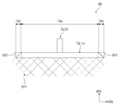
복수의 접속전극들은 제1 접속전극들(TSL1a~TSL1d) 및 제2 접속전극들(TSL2a~TSL2e)을 포함한다. The plurality of connection electrodes includes first connection electrodes TSL1a to TSL1d and second connection electrodes TSL2a to TSL2e.
제1 접속전극들(TSL1a~TSL1d)은 제2 방향(DR2)으로 나열되며, 제1 터치센서들의 끝단들에 각각 연결된다. 자세하게, 첫 번째 접속전극(TSL1a)은 제1 터치센서들 중 첫 번째 제1 터치센서의 끝단에 연결된다. 두 번째 접속전극(TSL1b)은 제1 터치센서들 중 두 번째 제1 터치센서의 끝단에 연결된다. 세 번째 접속전극(TSL1c)은 제1 터치센서들 중 세 번째 제1 터치센서의 끝단에 연결된다. 네 번째 접속전극(TSL1d)은 제1 터치센서들 중 네 번째 제1 터치센서의 끝단에 연결된다. 이처럼, 제1 접속전극들(TSL1a~TSL1d)은 제1 터치센서들의 끝단들에 각각 연결되어, 제1 터치센서들에 전기적 신호를 제공할 수 있다. The first connection electrodes TSL1a to TSL1d are arranged in the second direction DR2 and are respectively connected to ends of the first touch sensors. In detail, the first connection electrode TSL1a is connected to the end of the first first touch sensor among the first touch sensors. The second connection electrode TSL1b is connected to an end of the second first touch sensor among the first touch sensors. The third connection electrode TSL1c is connected to the end of the third first touch sensor among the first touch sensors. The fourth connection electrode TSL1d is connected to the end of the fourth first touch sensor among the first touch sensors. As such, the first connection electrodes TSL1a to TSL1d are respectively connected to ends of the first touch sensors to provide electrical signals to the first touch sensors.
제2 접속전극들(TSL2a~TSL2e)은 제1 방향(DR1)으로 나열되며, 제2 터치센서들의 끝단들에 각각 연결된다. 자세하게, 첫 번째 접속전극(TSL2a)은 제2 터치센서들 중 첫 번째 제2 터치센서의 끝단에 연결된다. 두 번째 접속전극(TSL2b)은 제2 터치센서들 중 두 번째 제2 터치센서의 끝단에 연결된다. 세 번째 접속전극(TSL2c)은 제2 터치센서들 중 세 번째 제2 터치센서의 끝단에 연결된다. 네 번째 접속전극(TSL2d)은 제2 터치센서들 중 네 번째 제2 터치센서의 끝단에 연결된다. 다섯 번째 접속전극(TSL2e)은 제2 터치센서들 중 다섯 번째 제2 터치센서의 끝단에 연결된다. 제2 접속전극들(TSL2a~TSL2e)은 제2 터치센서들의 끝단들에 각각 연결되어, 제2 터치센서들에 전기적 신호를 제공할 수 있다. The second connection electrodes TSL2a to TSL2e are arranged in a first direction DR1 and are respectively connected to ends of the second touch sensors. In detail, the first connection electrode TSL2a is connected to the end of the first second touch sensor among the second touch sensors. The second connection electrode TSL2b is connected to an end of the second second touch sensor among the second touch sensors. The third connection electrode TSL2c is connected to the end of the third second touch sensor among the second touch sensors. The fourth connection electrode TSL2d is connected to the end of the fourth second touch sensor among the second touch sensors. The fifth connection electrode TSL2e is connected to an end of the fifth second touch sensor among the second touch sensors. The second connection electrodes TSL2a to TSL2e are respectively connected to ends of the second touch sensors to provide electrical signals to the second touch sensors.
한편, 제1 접속전극들(TSL1a~TSL1d) 중 첫 번째 내지 세 번째 제1 접속전극들(TSL1a~TSL1c)은 평면영역(NBA)에 배치되고, 네 번째 제1 접속전극(TSL1d)은 밴딩영역(BA)에 배치된다. 일 예로서, 네 번째 제1 접속전극(TSL1d)이 밴딩영역(BA)에 배치된 것으로 설명되나, 밴딩영역(BA)에 하나 이상의 접속전극이 배치될 수 있다. 본 발명의 설명에 따르면, 하나의 접속전극이 밴딩영역(BA)에 배치된 것으로 설명된다. Meanwhile, of the first connection electrodes TSL1a to TSL1d, the first to third first connection electrodes TSL1a to TSL1c are disposed in the flat region NBA, and the fourth first connection electrode TSL1d is a bending region. It is placed in (BA). As an example, although the fourth first connection electrode TSL1d is described as being disposed in the bending area BA, one or more connection electrodes may be disposed in the bending area BA. According to the description of the present invention, it is described that one connection electrode is disposed in the bending area BA.
도 6b에 도시된 바에 따르면, 제1 접속전극들(TSL1a~TSL1d) 각각은 밴딩축(BX)에 수직한 제2 방향(DR2)으로 연장된 형상을 가진다. 본 발명에 따른 표시장치(DD)는 밴딩축(BX)을 기준으로 제2 방향(DR2)을 따라 밴딩된다. 그 결과, 제1 접속전극들(TSL1a~TSL1d) 중 밴딩영역(BA)에 배치된 네 번째 제1 접속전극(TSL1d)의 양단에 가해지는 응력이 제일 클 수 있다. 따라서, 네 번째 제1 접속전극(TSL1d)에 크랙(crack)이 발생될 수 있다. As shown in FIG. 6B, each of the first connection electrodes TSL1a to TSL1d has a shape extending in a second direction DR2 perpendicular to the bending axis BX. The display device DD according to the present invention is bent along the second direction DR2 with respect to the bending axis BX. As a result, among the first connection electrodes TSL1a to TSL1d, the stress applied to both ends of the fourth first connection electrode TSL1d disposed in the bending region BA may be the greatest. Accordingly, a crack may occur in the fourth first connection electrode TSL1d.
본 발명의 실시 예에 따르면, 네 번째 제1 접속전극(TSL1d)의 양측 엣지부분들 중 어느 하나의 엣지부분은 밴딩축(BX)과 경사진 엣지를 포함할 수 있다. 네 번째 제1 접속전극(TSL1d)의 어느 하나의 엣지부분이 밴딩축(BX)과 경사짐에 따라, 네 번째 제1 접속전극(TSL1d)의 양단에 가해지는 응력이 작아질 수 있다. According to an embodiment of the present invention, one of the edge portions on both sides of the fourth first connection electrode TSL1d may include a bending axis BX and an inclined edge. As any one edge portion of the fourth first connection electrode TSL1d is inclined with the bending axis BX, the stress applied to both ends of the fourth first connection electrode TSL1d may decrease.
이하에서, 제1 접속전극들(TSL1a~TSL1d) 및 제2 접속전극들(TSL2a~TSL2e)각각은 센터부분 및 양측 엣지부분들을 포함하는 것으로 설명된다. Hereinafter, each of the first connection electrodes TSL1a to TSL1d and the second connection electrodes TSL2a to TSL2e is described as including a center portion and both edge portions.
상술된 바와 같이, 본 발명에 따른 제1 접속전극들(TSL1a~TSL1d) 중 밴딩영역(BA)에 배치된 접속전극의 양측 엣지부분들 중 적어도 어느 하나는 밴딩축(BX)과 경사진 엣지를 포함할 수 있다. As described above, of the first connection electrodes TSL1a to TSL1d according to the present invention, at least one of the edge portions on both sides of the connection electrode disposed in the bending region BA has a bending axis BX and an inclined edge. Can include.
복수의 터치신호배선들은 제1 터치신호배선들(SPL1a~SPL1d) 및 제2 터치신호배선들(SPL2a~SPL2e)을 포함한다. 제1 터치신호배선들(SPL1a~SPL1d)의 일단들은 제1 접속전극들(TSL1a~TSL1d)과 각각 연결된다. 제1 터치신호배선들(SPL1a~SPL1d)의 끝단들은 제1 패드부(PD1)에 포함된 패드들에 각각 연결된다. 제1 터치신호배선들(SPL1a~SPL1d)은 제1 패드부(PD1)로부터 출력된 전기적 신호를 제1 접속전극들(TSL1a~TSL1d)에 전달한다. The plurality of touch signal wires includes first touch signal wires SPL1a to SPL1d and second touch signal wires SPL2a to SPL2e. One ends of the first touch signal lines SPL1a to SPL1d are respectively connected to the first connection electrodes TSL1a to TSL1d. End ends of the first touch signal lines SPL1a to SPL1d are respectively connected to pads included in the first pad part PD1. The first touch signal wirings SPL1a to SPL1d transfer the electrical signal output from the first pad part PD1 to the first connection electrodes TSL1a to TSL1d.
제2 터치신호배선들(SPL2a~SPL2e)의 일단들은 제2 접속전극들(TSL2a~TSL2e)과 각각 연결된다. 제2 터치신호배선들(SPL2a~SPL2e)의 끝단들은 제1 패드부(PD1)에 포함된 패드들에 각각 연결된다. 제2 터치신호배선들(SPL2a~SPL1e)은 제2 패드부(PD2)로부터 출력된 전기적 신호를 제2 접속전극들(TSL2a~TSL1e)에 전달한다.One ends of the second touch signal lines SPL2a to SPL2e are respectively connected to the second connection electrodes TSL2a to TSL2e. End ends of the second touch signal wires SPL2a to SPL2e are respectively connected to pads included in the first pad part PD1. The second touch signal wirings SPL2a to SPL1e transfer the electrical signal output from the second pad part PD2 to the second connection electrodes TSL2a to TSL1e.
도시되지 않았지만, 일 예로서, 제1 터치신호배선들(SPL1a~SPL1d) 및 제2 터치신호배선들(SP2a~SP2e)은 메쉬 형상을 가질 수 있다. Although not shown, as an example, the first touch signal wires SPL1a to SPL1d and the second touch signal wires SP2a to SP2e may have a mesh shape.
본 발명의 실시 예에 따르면, 제1 센서부들(SP1), 제1 연결부들(CP1), 및 제1 터치신호배선들(SPL1a~SPL1d), 제2 센서부들(SP2), 제2 연결부들(CP2), 및 제2 터치신호배선들(SPL2a~SPL2e) 중 일부는 도 6a에 도시된 제1 도전층(TS-CL1)을 패터닝하여 형성하고, 다른 일부는 도 6a에 도시된 제2 도전층(TS-CL2)을 패터닝하여 형성할 수 있다.According to an embodiment of the present invention, the first sensor units SP1, the first connection units CP1, and the first touch signal wirings SPL1a to SPL1d, the second sensor units SP2, and the second connection units ( CP2), and some of the second touch signal wirings SPL2a to SPL2e are formed by patterning the first conductive layer TS-CL1 shown in FIG. 6A, and another part is the second conductive layer shown in FIG. 6A It can be formed by patterning (TS-CL2).
다른 층 상에 배치된 도전 패턴들을 전기적으로 연결하기 위해, 도 6a에 도시된 제1 터치 절연층(TS-IL1)을 관통하는 콘택홀을 형성할 수 있다. 이하, 도 6c 내지 도 6e를 참조하여 일 실시 예에 따른 터치감지유닛(TS)을 설명한다.In order to electrically connect the conductive patterns disposed on other layers, a contact hole may be formed through the first touch insulating layer TS-IL1 shown in FIG. 6A. Hereinafter, a touch sensing unit TS according to an exemplary embodiment will be described with reference to FIGS. 6C to 6E.
도 6c에 도시된 것과 같이, 박막 봉지층(TFE) 상에 제1 도전패턴들이 배치된다. 제1 도전패턴들은 제2 연결부들(CP2)을 포함할 수 있다. 제2 연결부들(CP2)이 박막 봉지층(TFE) 상에 직접 배치된다. 표시영역(DA)을 커버하는 박막 봉지층(TFE)을 예시적으로 도시하였다. As shown in FIG. 6C, first conductive patterns are disposed on the thin film encapsulation layer TFE. The first conductive patterns may include second connection portions CP2. The second connection portions CP2 are directly disposed on the thin film encapsulation layer TFE. The thin film encapsulation layer TFE covering the display area DA is illustrated as an example.
도 6d에 도시된 것과 같이, 박막 봉지층(TFE) 상에 제2 연결부들(CP2)을 커버하는 제1 터치 절연층(TS-IL1)이 배치된다. 제1 터치 절연층(TS-IL1)에는 제2 연결부들(CP2)을 부분적으로 노출시키는 콘택홀들(CH)이 정의된다. 포토리소그래피 공정에 의해 콘택홀들(CH)이 형성될 수 있다.As shown in FIG. 6D, a first touch insulating layer TS-IL1 covering the second connection portions CP2 is disposed on the thin film encapsulation layer TFE. Contact holes CH partially exposing the second connection parts CP2 are defined in the first touch insulating layer TS-IL1. Contact holes CH may be formed by a photolithography process.
도 6e에 도시된 것과 같이, 제1 터치 절연층(TS-IL1) 상에 제2 도전패턴들이 배치된다. 제2 도전패턴들은 제1 센서부들(SP1), 제1 연결부들(CP1), 및 제1 터치신호배선들(SPL1a~SPL1d), 제2 터치 센서부들(SP2) 및 제2 터치신호배선들(SPL2a~SPL2e)을 포함할 수 있다. 별도로 도시하지 않았으나, 제1 터치 절연층(TS-IL1) 상에 제2 도전패턴들을 커버하는 제2 터치 절연층(TS-IL2)이 배치된다. As shown in FIG. 6E, second conductive patterns are disposed on the first touch insulating layer TS-IL1. The second conductive patterns include the first sensor parts SP1, the first connection parts CP1, and the first touch signal wires SPL1a to SPL1d, the second touch sensor parts SP2, and the second touch signal wires ( SPL2a to SPL2e) may be included. Although not shown separately, a second touch insulating layer TS-IL2 is disposed on the first touch insulating layer TS-IL1 to cover the second conductive patterns.
또한, 본 발명의 다른 실시 예에 따르면, 제1 도전패턴들과 제2 도전패턴들은 서로 바뀔 수 있다. 즉, 제2 도전패턴들이 제2 연결부들(CP2)을 포함할 수 있다.Further, according to another embodiment of the present invention, the first conductive patterns and the second conductive patterns may be interchanged with each other. That is, the second conductive patterns may include the second connection portions CP2.
도 7a는 본 발명의 실시 예에 따른 도 6e에 도시된 AA 영역을 확대한 확대도이다. 도 7b는 본 발명의 실시 예에 따른 도 7a에 도시된 센서패턴의 확대도이다. 도 7c는 본 발명의 실시 예에 따른 도 6e에 도시된 BB 영역을 확대한 확대도이다. 도 7d는 도 7c에 도시된 AX1 영역을 확대한 확대도이다. 도 7e는 도 7c에 도시된 AX2 영역을 확대한 확대도이다. 도 7f 및 도 7g는 본 발명의 다른 실시 예에 따른 도 6e에 도시된 BB 영역을 확대한 확대도이다. 7A is an enlarged view of an AA area shown in FIG. 6E according to an embodiment of the present invention. 7B is an enlarged view of the sensor pattern shown in FIG. 7A according to an embodiment of the present invention. FIG. 7C is an enlarged view of an enlarged BB area shown in FIG. 6E according to an embodiment of the present invention. 7D is an enlarged view of an area AX1 shown in FIG. 7C. 7E is an enlarged view of an AX2 area shown in FIG. 7C. 7F and 7G are enlarged views of an area BB shown in FIG. 6E according to another embodiment of the present invention.
도 7a를 참조하면, 도 6b에 도시된 제1 터치센서들 및 제2 터치센서들 각각은 복수의 메쉬 개구부들(TS-OP)을 정의하는 복수의 메쉬선들(SPt)을 포함한다. 메쉬선들(SPt)은 비발광영역(NPXA)에 중첩한다. 메쉬선들(SPt) 각각은 제1 방향(DR1) 및 제2 방향(DR2)과 교차하는 제5 방향(DR5)으로 연장하는 두 개의 제1 연장부들(SPt1-A)과 제5 방향(DR5)과 교차하는 제6 방향(DR6)으로 연장하는 두 개의 제2 연장부들(SPt1-B)을 포함한다. 제1 연장부들(SPt-A)은 서로 대향하며, 제2 연장부들(SPt-B)에 연결될 수 있다. 제2 연장부들(SPt-B)은 서로 대향하며, 제1 연장부들(SPt-A)에 연결될 수 있다. 메쉬선의 선폭은 수 마이크로일 수 있다.Referring to FIG. 7A, each of the first and second touch sensors shown in FIG. 6B includes a plurality of mesh lines SPt defining a plurality of mesh openings TS-OP. The mesh lines SPt overlap the non-emission area NPXA. Each of the mesh lines SPt includes two first extension portions SPt1-A and a fifth direction DR5 extending in a fifth direction DR5 intersecting the first direction DR1 and the second direction DR2. And two second extension portions SPt1 -B extending in the sixth direction DR6 intersecting with each other. The first extension parts SPt-A face each other and may be connected to the second extension parts SPt-B. The second extension parts SPt-B face each other and may be connected to the first extension parts SPt-A. The line width of the mesh line may be several microns.
한편, 메쉬 개구부들(TS-OP)이 발광영역들(PXA)에 일대일 대응하는 것으로 도시하였으나, 이에 제한되지 않는다. 하나의 메쉬 개구부(TS-OP)는 두 개 이상의 발광영역들(PXA)에 대응할 수 있다. Meanwhile, although the mesh openings TS-OP are shown to correspond to the light emitting regions PXA one-to-one, the present invention is not limited thereto. One mesh opening TS-OP may correspond to two or more light emitting regions PXA.
본 발명의 실시 예에 따르면, 메쉬 개구부들(TS-OP)은 제1 면적의 제1 메쉬 개구부들(TS-OP1) 및 제1 면적과 다른 제2 면적의 제2 메쉬 개구부들(TS-OP2)을 포함할 수 있다. According to an exemplary embodiment of the present invention, the mesh openings TS-OP include first mesh openings TS-OP1 having a first area and second mesh openings TS-OP2 having a second area different from the first area. ) Can be included.
발광영역들(PXA)의 크기는 다양할 수 있다. 일 예로서, 발광영역들(PXA) 중 제1 광을 제공하는 발광영역들(PXA)과 제2 광을 제공하는 발광영역들(PXA)의 크기는 서로 상이할 수 있다. 일 예로서, 발광영역들(PXA) 중 제1 광을 제공하는 발광영역들(PXA), 제2 광을 제공하는 발광영역들(PXA), 및 제3 광을 제공하는 발광영역들(PXA)의 크기는 서로 상이할 수 있다.The size of the emission areas PXA may vary. As an example, among the emission areas PXA, sizes of the emission areas PXA providing first light and the emission areas PXA providing second light may be different from each other. As an example, of the light-emitting areas PXA, the light-emitting areas PXA providing first light, the light-emitting areas PXA providing second light, and the light-emitting areas PXA providing third light The sizes of may be different from each other.
그러나, 본 발명의 기술적 사상은 이에 한정되지 않으며, 발광영역들(PXA)의 크기는 서로 동일할 수 있고, 또한 메쉬 개구부들(TS-OP)의 크기도 서로 동일할 수 있다.However, the technical idea of the present invention is not limited thereto, and the sizes of the light emitting areas PXA may be the same, and the sizes of the mesh openings TS-OP may be the same.
도 7b를 참조하면, 복수의 메쉬선들(SPt) 중 어느 하나의 메쉬선이 도시된다. 도 7b에 도시된 바에 따르면, 메쉬선(SPt)은 제1 연장부들(SPt-A)에 대응하는 제1 메쉬선(ML1) 및 제2 메쉬선(ML2)을 포함한다. 메쉬선(SPt)은 제2 연장부들(SPt-B)에 대응하는 제3 메쉬선(ML3) 및 제4 메쉬선(ML4)을 포함한다. Referring to FIG. 7B, any one of a plurality of mesh lines SPt is shown. As shown in FIG. 7B, the mesh line SPt includes a first mesh line ML1 and a second mesh line ML2 corresponding to the first extension parts SPt-A. The mesh line SPt includes a third mesh line ML3 and a fourth mesh line ML4 corresponding to the second extension parts SPt-B.
제1 메쉬선(ML1)의 일단은 제3 메쉬선(ML3)의 일단과 연결되며, 끝단은 제4 메쉬선(ML4)의 일단과 연결될 수 있다. 제2 메쉬선(ML2)의 일단은 제3 메쉬선(ML3)의 끝단과 연결되며, 끝단은 제4 메쉬선(ML4)의 끝단과 연결될 수 있다. One end of the first mesh line ML1 may be connected to one end of the third mesh line ML3, and the end may be connected to one end of the fourth mesh line ML4. One end of the second mesh line ML2 may be connected to an end of the third mesh line ML3, and an end of the second mesh line ML4 may be connected to an end of the fourth mesh line ML4.
본 발명의 실시 예에 따르면, 메쉬선(SPt)의 내측선(IML)은 밴딩축(BX)과 경사질 수 있다. 여기서, 내측선(IML)은 터치 개구부(TS-OP)를 정의하는 메쉬선(SPt)의 내측 테두리일 수 있다. 즉, 내측선(IML)이 밴딩축(BX)과 경사짐에 따라, 메쉬선(SPt)의 전반적인 형상이 밴딩축(BX)에 경사질 수 있다. 그 결과, 밴딩영역(BA)에서 메쉬선(SPt)에 가해지는 응력의 세기가 줄어들 수 있다. According to an embodiment of the present invention, the inner line IML of the mesh line SPt may be inclined with the bending axis BX. Here, the inner line IML may be an inner edge of the mesh line SPt defining the touch opening TS-OP. That is, as the inner line IML is inclined with the bending axis BX, the overall shape of the mesh line SPt may be inclined to the bending axis BX. As a result, the strength of the stress applied to the mesh line SPt in the bending area BA may be reduced.
도 7c를 참조하면, 본 발명의 일 실시 예에 따른 접속전극이 도시된다. 도 7c에 도시된 접속전극은 도 6b에 도시된 네 번째 접속전극(TSL1d)과 동일할 수 있다. 이하, 설명의 편의상, 네 번째 접속전극(TSL1d)는 접속전극(TSL1d)으로 설명된다. Referring to FIG. 7C, a connection electrode according to an embodiment of the present invention is shown. The connection electrode shown in FIG. 7C may be the same as the fourth connection electrode TSL1d shown in FIG. 6B. Hereinafter, for convenience of explanation, the fourth connection electrode TSL1d is described as a connection electrode TSL1d.
접속전극(TSL1d)은 센터부분(TAa), 제1 엣지부분(TAb), 및 제2 엣지부분(TAc)을 포함한다. 센터부분(TAa)은 제1 터치센서들 중 밴딩영역(BA)에 배치된 제1 터치센서의 끝단에 접촉된다. 제1 엣지부분(TAb)은 센터부분(TAa)의 일단에 연결될 수 있다. 제2 엣지부분(TAc)은 센터부분(TAa) 끝단에 연결될 수 있다. The connection electrode TSL1d includes a center portion TAa, a first edge portion TAb, and a second edge portion TAc. The center portion TAa is in contact with an end of the first touch sensor disposed in the bending area BA among the first touch sensors. The first edge portion TAb may be connected to one end of the center portion TAa. The second edge portion TAc may be connected to an end of the center portion TAa.
도 7d를 참조하면, 본 발명의 실시 예에 따른 제1 엣지부분(TAb)은 밴딩축(BX)과 수직한 제1 엣지(Ed1a) 및 밴딩축(BX)과 경사진 제2 엣지(Ed1b)를 포함한다. 즉, 제1 엣지(Ed1a)는 제2 방향(DR2)에 평행하며 제1 터치센서들 중 밴딩영역(BX)에 배치된 제1 터치센서의 끝단에 연결된다. 제2 엣지(Ed1b)는 제1 엣지(Ed1a) 및 센터부분(TAa)에 연결된다. Referring to FIG. 7D, a first edge portion TAb according to an embodiment of the present invention includes a first edge Ed1a perpendicular to the bending axis BX and a second edge inclined with the bending axis BX. Includes. That is, the first edge Ed1a is parallel to the second direction DR2 and is connected to an end of the first touch sensor disposed in the bending area BX among the first touch sensors. The second edge Ed1b is connected to the first edge Ed1a and the center portion TAa.
도 7e를 참조하면, 본 발명의 실시 예에 따른 제2 엣지부분(TAc)은 밴딩축(BX)과 수직한 제3 엣지(Ed2a) 및 밴딩축(BX)과 경사진 제4 엣지(Ed2b)를 포함한다. 즉, 제3 엣지(Ed2a)는 제2 방향(DR2)에 평행하며 제1 터치센서들 중 밴딩영역(BX)에 배치된 제1 터치센서의 끝단에 연결된다. 제4 엣지(Ed2b)는 제3 엣지(Ed2a) 및 센터부분(TAa)에 연결된다. Referring to FIG. 7E, a second edge portion TAc according to an embodiment of the present invention includes a third edge Ed2a perpendicular to the bending axis BX, and a fourth edge inclined with the bending axis BX. Includes. That is, the third edge Ed2a is parallel to the second direction DR2 and is connected to an end of the first touch sensor disposed in the bending area BX among the first touch sensors. The fourth edge Ed2b is connected to the third edge Ed2a and the center portion TAa.
또한, 본 발명의 실시 예에 따르면, 제1 엣지부분(TAb) 및 제2 엣지부분(TAc)은 밴딩축(BX)을 기준으로 서로 대칭될 수 있다. 그러나, 본 발명의 기술적 사상은 이에 한정되지 않으며, 제1 엣지부분(TAb) 및 제2 엣지부분(TAc)은 서로 다른 형상을 가질 수 있다. 일 예로서, 접속전극의 제1 엣지부분은 평면영역(NBA)에 배치되고, 접속전극의 제2 엣지부분은 밴딩영역(BA)에 배치될 수 있다. 이 경우, 평면영역(NBA)에 배치된 제1 엣지부분과 밴딩영역(BA)에 배치된 제2 엣지부분의 형상은 서로 다를 수 있다. In addition, according to an embodiment of the present invention, the first edge portion TAb and the second edge portion TAc may be symmetrical to each other with respect to the bending axis BX. However, the technical idea of the present invention is not limited thereto, and the first edge portion TAb and the second edge portion TAc may have different shapes. As an example, a first edge portion of the connection electrode may be disposed in the flat area NBA, and a second edge portion of the connection electrode may be disposed in the bending area BA. In this case, the shape of the first edge portion disposed in the flat area NBA and the second edge portion disposed in the bending area BA may be different from each other.
또한, 본 발명의 실시 예에 따르면, 밴딩축(BX)을 기준으로 제2 엣지(Ed1b)의 기울기는 도 7b에 도시된 제3 메쉬선(ML3)의 기울기와 동일할 수 있다. 밴딩축(BX)을 기준으로 제4 엣지부분(Ed2b)의 기울기는 도 7b에 도시된 제2 메쉬선(ML2)의 기울기와 동일할 수 있다. Further, according to an embodiment of the present invention, the slope of the second edge Ed1b based on the bending axis BX may be the same as the slope of the third mesh line ML3 illustrated in FIG. 7B. The slope of the fourth edge portion Ed2b based on the bending axis BX may be the same as the slope of the second mesh line ML2 illustrated in FIG. 7B.
도 7f를 참조하면, 본 발명의 다른 실시 예에 따른 접속전극의 양측 엣지부분들 중 어느 하나의 엣지부분이 설명된다. Referring to FIG. 7F, an edge portion of any one of the edge portions of both sides of a connection electrode according to another embodiment of the present invention will be described.
제3 엣지(Ed2c)는 제2 방향(DR2)에 평행하며 제4 엣지(Ed2d) 및 센터부분(TAa)에 연결된다. 제4 엣지(Ed2d)는 밴딩축(BX)과 경사지며 제3 엣지(Ed2c) 및 센터부분(TAa)에 연결된다. 이 경우, 제3 엣지(Ed2c) 및 제4 엣지(Ed2d) 각각은 제1 터치센서의 끝단으로부터 이격될 수 있다. The third edge Ed2c is parallel to the second direction DR2 and is connected to the fourth edge Ed2d and the center portion TAa. The fourth edge Ed2d is inclined with the bending axis BX and is connected to the third edge Ed2c and the center portion TAa. In this case, each of the third edge Ed2c and the fourth edge Ed2d may be spaced apart from the end of the first touch sensor.
즉, 제3 엣지(Ed2c)의 일단은 제4 엣지(Ed2d)의 일단에 연결되며, 끝단은 센터부분(TAa)에 연결된다. 제4 엣지(Ed2d)의 일단은 센터부분(TAb)과 연결되며, 끝단은 제3 엣지(Ed2c)에 연결된다. That is, one end of the third edge Ed2c is connected to one end of the fourth edge Ed2d, and the end is connected to the center portion TAa. One end of the fourth edge Ed2d is connected to the center portion TAb, and the end is connected to the third edge Ed2c.
도 7g 및 도 7i를 참조하면, 도 7c에 도시된 접속전극(TSL1d)과 다른 접속전극이 도시된다. 도 7g 및 도 7i에 도시된 접속전극(TSL1d)은 도 7c에 도시된 접속전극(TSL1d)과 비교하여, 제1 엣지부분(TAb) 및 제2 엣지부분(TAc)의 형상이 다를 뿐 나머지 구조는 실질적으로 동일할 수 있다. 따라서, 도 7g 및 도 7i를 통해 제1 엣지부분 및 제2 엣지부분의 형상이 구체적으로 설명된다. 7G and 7I, a connection electrode different from the connection electrode TSL1d shown in FIG. 7C is shown. The connection electrode TSL1d shown in FIGS. 7G and 7I differs from the connection electrode TSL1d shown in FIG. 7C, but the shape of the first edge portion TAb and the second edge portion TAc is different. May be substantially the same. Accordingly, the shapes of the first edge portion and the second edge portion will be described in detail through FIGS. 7G and 7I.
먼저, 도 7f를 참조하면, 접속전극(TSL1d)은 센터부분(TA2a), 제1 엣지부분(TA2b), 및 제2 엣지부분(TA2c)을 포함한다. First, referring to FIG. 7F, the connection electrode TSL1d includes a center portion TA2a, a first edge portion TA2b, and a second edge portion TA2c.
본 발명의 실시 예에 따르면, 제1 엣지부분(TA2b)은 제5 엣지(Ed3a) 및 제6 엣지(Ed3b)를 포함할 수 있다. 제2 엣지부분(TA2c)은 제7 엣지(Ed4a) 및 제8 엣지(Ed4b)를 포함할 수 있다. According to an embodiment of the present invention, the first edge portion TA2b may include a fifth edge Ed3a and a sixth edge Ed3b. The second edge portion TA2c may include a seventh edge Ed4a and an eighth edge Ed4b.
특히, 본 발명에 따른 제5 엣지(Ed3a) 및 제6 엣지(Ed3b) 각각은 밴딩축(BX)과 경사질 수 있다. 즉, 제5 엣지(Ed3a)의 일단은 제6 엣지(Ed3b)의 일단과 연결되고, 끝단은 센터부분(TA2a)에 연결된다. 제6 엣지(Ed3b)의 일단은 제5 엣지(Ed3a)의 일단에 연결되고, 끝단은 센터부분(TA2a)에 연결될 수 있다. In particular, each of the fifth edge Ed3a and the sixth edge Ed3b according to the present invention may be inclined with the bending axis BX. That is, one end of the fifth edge Ed3a is connected to one end of the sixth edge Ed3b, and the end is connected to the center portion TA2a. One end of the sixth edge Ed3b may be connected to one end of the fifth edge Ed3a, and the end may be connected to the center portion TA2a.
이처럼, 제5 엣지(Ed3a)의 일단 및 제6 엣지(Ed3b)의 일단이 서로 연결됨에 따라, 제5 엣지(Ed3a) 및 제6 엣지(Ed3b) 각각은 제1 터치센서의 끝단과 이격되어 밴딩축(BX)에 경사질 수 있다. In this way, as one end of the fifth edge Ed3a and one end of the sixth edge Ed3b are connected to each other, each of the fifth edge Ed3a and the sixth edge Ed3b is separated from the end of the first touch sensor and bends. It can be inclined to the axis (BX).
또한, 제7 엣지(Ed4a) 및 제8 엣지(Ed4b) 각각도 밴딩축(BX)과 경사질 수 있다. 즉, 제7 엣지(Ed4a)의 일단은 제8 엣지(Ed4b)의 일단과 연결되고, 끝단은 센터부분(TA2a)에 연결된다. 제8 엣지(Ed4b)의 일단은 제7 엣지(Ed4a)의 일단에 연결되고, 끝단은 센터부분(TA2a)에 연결될 수 있다. In addition, each of the seventh edge Ed4a and the eighth edge Ed4b may also be inclined with the bending axis BX. That is, one end of the seventh edge Ed4a is connected to one end of the eighth edge Ed4b, and the end is connected to the center portion TA2a. One end of the eighth edge Ed4b may be connected to one end of the seventh edge Ed4a, and the end may be connected to the center portion TA2a.
이처럼, 제7 엣지(Ed4a)의 일단 및 제8 엣지(Ed4b)의 일단이 서로 연결됨에 따라, 제7 엣지(Ed4a) 및 제8 엣지(Ed4b) 각각은 제1 터치센서의 끝단과 이격되어 밴딩축(BX)에 경사질 수 있다. In this way, as one end of the seventh edge Ed4a and one end of the eighth edge Ed4b are connected to each other, each of the seventh edge Ed4a and the eighth edge Ed4b is bent apart from the end of the first touch sensor. It can be inclined to the axis (BX).
도 7i를 참조하면, 접속전극(TSL1d)은 센터부분(TA3a), 제1 엣지부분(TA3b), 및 제2 엣지부분(TA3c)을 포함한다. Referring to FIG. 7I, the connection electrode TSL1d includes a center portion TA3a, a first edge portion TA3b, and a second edge portion TA3c.
제1 엣지부분(TA3b)은 제9 엣지(Ed5a), 제10 엣지(Ed5b), 및 제11 엣지(Ed5c)를 포함할 수 있다. 제11 엣지(Ed5c)는 제9 엣지(Ed5a) 및 제10 엣지(Ed5b)를 서로 연결할 수 있다. The first edge portion TA3b may include a ninth edge Ed5a, a tenth edge Ed5b, and an eleventh edge Ed5c. The eleventh edge Ed5c may connect the ninth edge Ed5a and the tenth edge Ed5b to each other.
실시 예에 따르면, 제9 엣지(Ed5a), 제10 엣지(Ed5b)는 밴딩축(BX)과 경사질 수 있으며, 제11 엣지(Ed5c)는 밴딩축(BX)과 평행할 수 있다. 그러나, 이에 한정되지 않으며, 제11 엣지(Ed5c)는 밴딩축(BX)과 경사질 수 있다. 즉, 본 발명에 따른 제9 내지 제11 엣지들(Ed5a~Ed5c)은 밴딩축(BX)과 수직하는 부분이 없음에 따라, 밴딩영역(BA)에서 제9 내지 제11 엣지들(Ed5a~Ed5c)에 가해지는 응력이 감소될 수 있다. According to an embodiment, the ninth edge Ed5a and the tenth edge Ed5b may be inclined with the bending axis BX, and the eleventh edge Ed5c may be parallel to the bending axis BX. However, the present invention is not limited thereto, and the eleventh edge Ed5c may be inclined with the bending axis BX. That is, since the ninth to eleventh edges Ed5a to Ed5c according to the present invention do not have a portion perpendicular to the bending axis BX, the ninth to eleventh edges Ed5a to Ed5c in the bending area BA. ) Can be reduced.
제2 엣지부분(TA3c)은 제12 엣지(Ed6a), 제13 엣지(Ed6b), 및 제14 엣지(Ed6c)를 포함할 수 있다. 제14 엣지(Ed6c)는 제12 엣지(Ed6a) 및 제13 엣지(Ed6b)를 서로 연결할 수 있다. The second edge portion TA3c may include a twelfth edge Ed6a, a thirteenth edge Ed6b, and a fourteenth edge Ed6c. The 14th edge Ed6c may connect the 12th edge Ed6a and the 13th edge Ed6b to each other.
실시 예에 따르면, 제12 엣지(Ed6a), 제13 엣지(Ed6b)는 밴딩축(BX)과 경사질 수 있으며, 제14 엣지(Ed6c)는 밴딩축(BX)과 평행할 수 있다. 그러나, 이에 한정되지 않으며, 제14 엣지(Ed6c)는 밴딩축(BX)과 경사질 수 있다. 즉, 본 발명에 따른 제12 내지 제14 엣지들(Ed6a~Ed6c)은 밴딩축(BX)과 수직하는 부분이 없음에 따라, 밴딩영역(BA)에서 제12 내지 제14 엣지들(Ed6a~Ed6c)에 가해지는 응력이 감소될 수 있다. According to an embodiment, the twelfth edge Ed6a and the thirteenth edge Ed6b may be inclined with the bending axis BX, and the 14th edge Ed6c may be parallel to the bending axis BX. However, the present invention is not limited thereto, and the 14th edge Ed6c may be inclined with the bending axis BX. That is, since the twelfth to fourteenth edges Ed6a to Ed6c according to the present invention do not have a portion perpendicular to the bending axis BX, the twelfth to fourteenth edges Ed6a to Ed6c in the bending area BA. ) Can be reduced.
상술된 바와 같이, 본 발명의 실시 예에 따르면, 밴딩영역(BA)에 배치된 접속전극의 엣지부분들은 밴딩축(BX)과 경사진 엣지를 포함할 수 있다. 따라서, 접속전극의 엣지부분들에 가해지는 응력이 감소되며, 표시장치(DD)의 밴딩에 따른 접속전극의 양단에서의 크랙이 방지될 수 있다. As described above, according to the embodiment of the present invention, edge portions of the connection electrode disposed in the bending area BA may include the bending axis BX and an inclined edge. Accordingly, stress applied to the edge portions of the connection electrode is reduced, and cracks at both ends of the connection electrode due to bending of the display device DD can be prevented.
한편, 도 7c 내지 도 7i를 통해 접속전극의 엣지부분들의 형상이 설명되었으나, 본 발명의 기술적 사상은 이에 한정되지 않는다. 즉, 접속전극 엣지부분들의 형상은 밴딩영역(BX)에서 밴딩축(BX)을 기반으로 다양하게 변형될 수 있다. Meanwhile, the shape of the edge portions of the connection electrode has been described through FIGS. 7C to 7I, but the technical idea of the present invention is not limited thereto. That is, the shape of the edge portions of the connection electrode may be variously modified in the bending area BX based on the bending axis BX.
또한, 일 예로서, 접속전극의 엣지부분들 중 어느 하나의 엣지부분은 도 7d에 도시된 엣지부분으로 구현되며, 다른 하나의 엣지부분은 도 7f에 도시된 엣지부분으로 구현될 수 있다. 즉, 본 발명의 접속전극의 엣지부분들은 다양한 형상으로 제공될 수 있다. In addition, as an example, one of the edge portions of the connection electrode may be implemented as an edge portion shown in FIG. 7D, and the other edge portion may be implemented as an edge portion shown in FIG. 7F. That is, the edge portions of the connection electrode of the present invention may be provided in various shapes.
도 8a는 본 발명의 다른 실시 예에 따른 터치감지유닛의 평면도이다. 도 8b는 본 발명의 실시 예에 따른 도 8a에 도시된 CC 영역을 확대한 확대도이다. 8A is a plan view of a touch sensing unit according to another embodiment of the present invention. FIG. 8B is an enlarged view of an enlarged CC area shown in FIG. 8A according to an embodiment of the present invention.
도 8a에 도시된 터치감지유닛(TS2)은 도 6b에 도시된 터치감지유닛(TS1)과 비교하여, 터치신호배선들의 구조가 변경되었을 뿐, 나머지 구성들은 실질적으로 동일할 수 있다. 따라서, 나머지 구성들에 대한 설명은 생략된다. Compared to the touch sensing unit TS1 illustrated in FIG. 6B, the touch sensing unit TS2 illustrated in FIG. 8A has only changed the structure of the touch signal wirings, and the remaining configurations may be substantially the same. Therefore, description of the remaining components is omitted.
도 8a 및 도 8b를 참조하면, 제1 터치신호배선들(SPL1a~SPL1d) 및 제2 터치신호배선들(SPL2a~SPL2e) 중 밴딩영역(BA)에 배치된 터치신호배선들의 일 부분은 밴딩축(BX)과 경사질 수 있다. 8A and 8B, a portion of the touch signal wirings arranged in the bending area BA among the first touch signal wirings SPL1a to SPL1d and the second touch signal wirings SPL2a to SPL2e is a bending axis. (BX) and can be inclined.
자세하게, 도 8a에 도시된 바와 같이, 평면영역(NBA)에는 밴딩축(BX)과 수직한 제2 방향(DR2)을 따라 연장된 신호배선들이 배치된다. 이 경우, 평면영역(NBA)이 밴딩되지 않음에 따라, 터치신호배선에 응력이 작용하지 않는다. 이와 반대로, 밴딩영역(BA)에 제2 방향(DR2)을 따라 연장된 터치신호배선들이 배치될 경우, 터치신호배선들에 응력이 가해질 수 있다. In detail, as shown in FIG. 8A, signal lines extending along the second direction DR2 perpendicular to the bending axis BX are disposed in the planar area NBA. In this case, since the flat area NBA is not bent, no stress is applied to the touch signal wiring. Conversely, when the touch signal wirings extending along the second direction DR2 are disposed in the bending area BA, a stress may be applied to the touch signal wirings.
이하에서, 첫 번째 제1 터치신호배선(SPL1a)과 제2 터치신호배선들이 밴딩영역(BA)에 배치된 것으로 설명된다. 그러나, 이에 한정되지 않으며, 터치신호배선들이 밴딩영역(BA)에 배치되는 구조는 접속전극들의 연결 구조에 따라 다양하게 변형될 수 있다. Hereinafter, it will be described that the first first touch signal wires SPL1a and the second touch signal wires are disposed in the bending area BA. However, the present invention is not limited thereto, and the structure in which the touch signal wires are arranged in the bending area BA may be variously modified according to the connection structure of the connection electrodes.
본 발명의 실시 예에 따르면, 터치신호배선들 중 밴딩영역(BA)에 배치된 터치신호배선은 밴딩축(BX)과 경사질 수 있다. 일 예로서, 평면영역(NBA)에 배치된 첫 번째 제1 터치신호배선(SPL1a) 부분이 제2 방향(DR2)을 따라 연장된다. 이 경우, 제1 터치신호배선(SPL1a)에 응력이 가해지지 않는다. According to an embodiment of the present invention, among the touch signal wirings, the touch signal wiring disposed in the bending area BA may be inclined with the bending axis BX. As an example, a portion of the first first touch signal line SPL1a disposed in the flat area NBA extends along the second direction DR2. In this case, no stress is applied to the first touch signal wiring SPL1a.
밴딩영역(BA)에 배치된 첫 번째 제1 터치신호배선(SPL1a)의 부분은 밴딩축(BX)과 경사지어, 제1 접속전극들 중 밴딩영역(BA)에 배치된 접속전극에 연결될 수 있다. 따라서, 밴딩영역(BA)에 배치된 첫 번째 제1 터치신호배선(SPL1a)의 부분에 작용하는 응력이 감소될 수 있다. A portion of the first first touch signal wiring SPL1a disposed in the bending area BA may be inclined with the bending axis BX, and may be connected to a connection electrode disposed in the bending area BA among the first connection electrodes. . Accordingly, the stress acting on the portion of the first first touch signal wiring SPL1a disposed in the bending area BA may be reduced.
특히, 도 8b에 도시된 바와 같이, 본 발명에 따른 터치신호배선들 중 밴딩영역(BA)에 배치된 터치신호배선은 밴딩축(BX)과 경사진 경사부분(CV) 및 밴딩축(BX)과 평행한 평행부분(PV)을 포함할 수 있다. In particular, as shown in FIG. 8B, among the touch signal wirings according to the present invention, the touch signal wiring arranged in the bending area BA has a bending axis BX, an inclined slope CV, and a bending axis BX. It may include a parallel portion (PV) parallel to.
이처럼, 본 발명에 따른 터치신호배선들은 밴딩영역(BA)에서 밴딩축(BX)과 경사지거나 평행함에 따라, 터치신호배선들에 가해지는 응력의 세기가 감소될 수 있다. As such, as the touch signal wirings according to the present invention are inclined or parallel to the bending axis BX in the bending area BA, the intensity of the stress applied to the touch signal wirings may be reduced.
도 9는 본 발명의 다른 실시 예에 따른 터치감지유닛의 평면도이다. 9 is a plan view of a touch sensing unit according to another embodiment of the present invention.
도 9에 도시된 터치감지유닛(TS3)은 도 6b도시된 터치감지유닛(TS)과 비교하여, 터치신호배선들 및 접속전극들의 구조가 달라졌을 뿐, 나머지 구성들은 실질적으로 동일할 수 있다. 따라서, 나머지 구성들에 대한 설명은 생략된다. Compared with the touch sensing unit TS of FIG. 6B, the touch sensing unit TS3 illustrated in FIG. 9 has a different structure of the touch signal wires and the connection electrodes, and the remaining configurations may be substantially the same. Therefore, description of the remaining components is omitted.
도 9를 참조하면, 제1 터치센서들의 일단들 및 끝단들 각각에 복수의 접속전극들이 연결될 수 있다. 자세하게, 제1 터치센서들의 일단들에 제1 접속전극들(TSL1)이 각각 연결되고, 끝단들에 제2 접속전극들(TSL2)이 각각 연결된다. 제2 터치센서들의 일단들에 제3 접속전극들(TSL3)이 각각 연결되고, 끝단들에 제4 접속전극들(TSL4)이 각각 연결된다. Referring to FIG. 9, a plurality of connection electrodes may be connected to each of one ends and ends of the first touch sensors. In detail, the first connection electrodes TSL1 are connected to one end of the first touch sensors, and the second connection electrodes TSL2 are connected to the ends. The third connection electrodes TSL3 are connected to one end of the second touch sensors, and the fourth connection electrodes TSL4 are connected to the ends.
제1 접속전극들(TSL1) 및 제2 접속전극들(TSL2)은 제1 방향(DR1)에서 서로 대향할 수 있다. 제3 접속전극들(TSL3) 및 제4 접속전극들(TSL4)은 제2 방향(DR2)에서 서로 대향할 수 있다. The first connection electrodes TSL1 and the second connection electrodes TSL2 may face each other in the first direction DR1. The third connection electrodes TSL3 and the fourth connection electrodes TSL4 may face each other in the second direction DR2.
한편, 제1 터치신호배선들은 제1 패드부(PDs1) 및 제1 접속전극들(TSL1)과 연결되어, 제1 패드부(PDs1)로부터 출력된 전기적 신호를 제1 접속전극들(TSL1)에 전달한다. 제2 터치신호배선들은 제2 패드부(PDs2) 및 제2 접속전극들(TSL2)과 연결되어, 제2 패드부(PDs2)로부터 출력된 전기적 신호를 제2 접속전극들(TSL2)에 전달한다. 제3 터치신호배선들은 제3 패드부(PDs3) 및 제3 접속전극들(TSL3)과 연결되어, 제3 패드부(PDs3)로부터 출력된 전기적 신호를 제3 접속전극들(TSL3)에 전달한다. 제4 터치신호배선들은 제4 패드부(PDs4) 및 제4 접속전극들(TSL4)과 연결되어, 제4 패드부(PDs4)로부터 출력된 전기적 신호를 제4 접속전극들(TSL4)에 전달한다.Meanwhile, the first touch signal wires are connected to the first pad part PDs1 and the first connection electrodes TSL1, so that an electrical signal output from the first pad part PDs1 is transmitted to the first connection electrodes TSL1. Deliver. The second touch signal wires are connected to the second pad part PDs2 and the second connection electrodes TSL2 to transmit the electrical signal output from the second pad part PDs2 to the second connection electrodes TSL2. . The third touch signal wires are connected to the third pad part PDs3 and the third connection electrodes TSL3 to transmit an electrical signal output from the third pad part PDs3 to the third connection electrodes TSL3. . The fourth touch signal wires are connected to the fourth pad part PDs4 and the fourth connection electrodes TSL4 to transmit an electrical signal output from the fourth pad part PDs4 to the fourth connection electrodes TSL4. .
도 8b를 통해 상술된 바와 마찬가지로, 밴딩영역(BA)에 배치된 제1 내지 제4 터치신호배선들은 밴딩축(BX)과 경사진 경사부분(CV) 및 밴딩축(BX)과 평행한 평행부분(PV)을 포함할 수 있다.As described above with reference to FIG. 8B, the first to fourth touch signal wirings disposed in the bending area BA are the bending axis BX, the inclined inclined portion CV, and the parallel portion parallel to the bending axis BX. (PV) may be included.
이상에서와 같이 도면과 명세서에서 실시 예가 개시되었다. 여기서 특정한 용어들이 사용되었으나, 이는 단지 본 발명을 설명하기 위한 목적에서 사용된 것이지 의미 한정이나 특허 청구범위에 기재된 본 발명의 범위를 제한하기 위하여 사용된 것은 아니다. 그러므로 본 기술분야의 통상의 지식을 가진 자라면 이로부터 다양한 변형 및 균등한 타 실시 예가 가능하다는 점을 이해할 것이다. 따라서 본 발명의 진정한 기술적 보호 범위는 첨부된 특허 청구범위의 기술적 사상에 의해 정해져야 할 것이다.As described above, embodiments have been disclosed in the drawings and specifications. Although specific terms have been used herein, these are only used for the purpose of describing the present invention, and are not used to limit the meaning or the scope of the present invention described in the claims. Therefore, those of ordinary skill in the art will understand that various modifications and equivalent other embodiments are possible therefrom. Therefore, the true technical protection scope of the present invention should be determined by the technical spirit of the appended claims.
DP: 표시패널
TS: 터치감지유닛
SP1: 제1 센서부
SP2: 제2 센서부
SPL: 터치신호배선DP: display panel
TS: Touch sensing unit
SP1: first sensor unit
SP2: second sensor unit
SPL: Touch signal wiring
Claims (7)
상기 베이스 층 상에 배치되고 복수의 화소들을 포함하는 표시 소자층;
상기 표시 소자층 상에 배치되어 상기 화소들을 커버하는 봉지층;
상기 봉지층 상에 배치되고, 각각이 메쉬 형상을 갖는 복수 개의 도전 패턴들을 포함하는 복수의 터치센서들; 및
상기 터치센서들에 각각 연결된 복수 개의 터치신호배선들을 포함하고,
상기 도전 패턴들은 복수 개의 메쉬 개구부들을 정의하는 복수 개의 메쉬선들을 포함하고,
서로 연결되어 상기 메쉬 개구부들 중 어느 하나를 정의하는 4 개의 메쉬선들의 내측선들은 상기 밴딩축에 대해 경사진 표시 장치.A base layer bent around a bending axis extending along one direction;
A display device layer disposed on the base layer and including a plurality of pixels;
An encapsulation layer disposed on the display device layer to cover the pixels;
A plurality of touch sensors disposed on the encapsulation layer and including a plurality of conductive patterns each having a mesh shape; And
Including a plurality of touch signal wirings each connected to the touch sensors,
The conductive patterns include a plurality of mesh lines defining a plurality of mesh openings,
Inner lines of four mesh lines that are connected to each other and define any one of the mesh openings are inclined with respect to the bending axis.
상기 4 개의 메쉬선들 각각은 연장된 방향을 따라 상이한 너비를 가진 표시 장치.The method of claim 1,
Each of the four mesh lines has a different width along an extended direction.
상기 4 개의 메쉬선들이 정의하는 개구부는 5 개 이상의 꼭지점들을 가진 표시 장치.The method of claim 2,
An opening defined by the four mesh lines has five or more vertices.
상기 4 개의 메쉬선들이 정의하는 개구부와 상기 개구부에 인접하는 개구부들은 서로 상이한 형상을 가진 표시 장치.The method of claim 3,
An opening defined by the four mesh lines and openings adjacent to the opening have different shapes from each other.
상기 베이스층은 상기 벤딩축을 중심으로 벤딩되는 벤딩영역을 포함하고,
상기 터치신호배선들 중 상기 벤딩영역에 배치된 터치신호배선들은 상기 밴딩축에 대해 경사진 부분들을 포함하는 표시 장치.The method of claim 1,
The base layer includes a bending region that is bent around the bending axis,
Among the touch signal wirings, the touch signal wirings arranged in the bending area include portions inclined with respect to the bending axis.
상기 터치신호배선들은 상기 터치센서들로부터 멀어질수록 더 많은 수의 경사진 부분들을 갖는 표시 장치.The method of claim 5,
The display device having a larger number of inclined portions as the touch signal wirings move away from the touch sensors.
상기 터치신호배선과 상기 도전패턴 사이에 배치되고, 상기 메쉬선들에 접속된 접속전극을 더 포함하고,
상기 접속전극은 상기 밴딩축에 대해 경사진 엣지를 포함하는 표시 장치.The method of claim 1,
A connection electrode disposed between the touch signal wiring and the conductive pattern and connected to the mesh lines,
The connection electrode includes an edge inclined with respect to the bending axis.
Priority Applications (4)
| Application Number | Priority Date | Filing Date | Title |
|---|---|---|---|
| KR1020200108422A KR102319542B1 (en) | 2019-08-28 | 2020-08-27 | Display device |
| KR1020210143050A KR102480860B1 (en) | 2020-08-27 | 2021-10-25 | Display device |
| KR1020220179350A KR102658896B1 (en) | 2020-08-27 | 2022-12-20 | Display device |
| KR1020240050165A KR20240054944A (en) | 2020-08-27 | 2024-04-15 | Display device |
Applications Claiming Priority (2)
| Application Number | Priority Date | Filing Date | Title |
|---|---|---|---|
| KR1020190105751A KR102151017B1 (en) | 2019-08-28 | 2019-08-28 | Display device |
| KR1020200108422A KR102319542B1 (en) | 2019-08-28 | 2020-08-27 | Display device |
Related Parent Applications (1)
| Application Number | Title | Priority Date | Filing Date |
|---|---|---|---|
| KR1020190105751A Division KR102151017B1 (en) | 2019-08-28 | 2019-08-28 | Display device |
Related Child Applications (1)
| Application Number | Title | Priority Date | Filing Date |
|---|---|---|---|
| KR1020210143050A Division KR102480860B1 (en) | 2020-08-27 | 2021-10-25 | Display device |
Publications (2)
| Publication Number | Publication Date |
|---|---|
| KR20200106014A true KR20200106014A (en) | 2020-09-10 |
| KR102319542B1 KR102319542B1 (en) | 2021-11-02 |
Family
ID=72469678
Family Applications (1)
| Application Number | Title | Priority Date | Filing Date |
|---|---|---|---|
| KR1020200108422A Active KR102319542B1 (en) | 2019-08-28 | 2020-08-27 | Display device |
Country Status (1)
| Country | Link |
|---|---|
| KR (1) | KR102319542B1 (en) |
Cited By (1)
| Publication number | Priority date | Publication date | Assignee | Title |
|---|---|---|---|---|
| WO2023176988A1 (en) * | 2022-03-14 | 2023-09-21 | 엘지전자 주식회사 | Display device for vehicle |
Citations (4)
| Publication number | Priority date | Publication date | Assignee | Title |
|---|---|---|---|---|
| EP2980680A1 (en) * | 2013-03-28 | 2016-02-03 | Fujikura, Ltd. | Touch sensor and production method for same |
| WO2016039047A1 (en) * | 2014-09-11 | 2016-03-17 | 富士フイルム株式会社 | Laminated structure, touch panel, display device with touch panel, and method for manufacturing same |
| JP2016076146A (en) * | 2014-10-08 | 2016-05-12 | 凸版印刷株式会社 | Touch panel |
| KR20160086489A (en) * | 2015-01-09 | 2016-07-20 | 삼성디스플레이 주식회사 | Flexible touch panel and flexible display device |
-
2020
- 2020-08-27 KR KR1020200108422A patent/KR102319542B1/en active Active
Patent Citations (4)
| Publication number | Priority date | Publication date | Assignee | Title |
|---|---|---|---|---|
| EP2980680A1 (en) * | 2013-03-28 | 2016-02-03 | Fujikura, Ltd. | Touch sensor and production method for same |
| WO2016039047A1 (en) * | 2014-09-11 | 2016-03-17 | 富士フイルム株式会社 | Laminated structure, touch panel, display device with touch panel, and method for manufacturing same |
| JP2016076146A (en) * | 2014-10-08 | 2016-05-12 | 凸版印刷株式会社 | Touch panel |
| KR20160086489A (en) * | 2015-01-09 | 2016-07-20 | 삼성디스플레이 주식회사 | Flexible touch panel and flexible display device |
Cited By (2)
| Publication number | Priority date | Publication date | Assignee | Title |
|---|---|---|---|---|
| WO2023176988A1 (en) * | 2022-03-14 | 2023-09-21 | 엘지전자 주식회사 | Display device for vehicle |
| EP4491431A4 (en) * | 2022-03-14 | 2025-05-14 | LG Electronics Inc. | VEHICLE DISPLAY DEVICE |
Also Published As
| Publication number | Publication date |
|---|---|
| KR102319542B1 (en) | 2021-11-02 |
Similar Documents
| Publication | Publication Date | Title |
|---|---|---|
| KR101904969B1 (en) | Display device | |
| US11755132B2 (en) | Display apparatus | |
| KR102601207B1 (en) | Display device | |
| EP3276460B1 (en) | Display device | |
| KR102017767B1 (en) | Display device | |
| KR102468358B1 (en) | Display apparatus | |
| KR102151017B1 (en) | Display device | |
| KR102319542B1 (en) | Display device | |
| KR102480860B1 (en) | Display device | |
| KR102702738B1 (en) | Display apparatus and method for manufacturing display apparatus | |
| KR102406621B1 (en) | Display device and method for fabricating the same | |
| KR102772217B1 (en) | Touch sensor and display device | |
| KR20220081324A (en) | Display device and method for fabricating the same |
Legal Events
| Date | Code | Title | Description |
|---|---|---|---|
| A107 | Divisional application of patent | ||
| PA0107 | Divisional application |
Comment text: Divisional Application of Patent Patent event date: 20200827 Patent event code: PA01071R01D Filing date: 20190828 Application number text: 1020190105751 |
|
| PA0201 | Request for examination | ||
| PG1501 | Laying open of application | ||
| E902 | Notification of reason for refusal | ||
| PE0902 | Notice of grounds for rejection |
Comment text: Notification of reason for refusal Patent event date: 20201127 Patent event code: PE09021S01D |
|
| E701 | Decision to grant or registration of patent right | ||
| PE0701 | Decision of registration |
Patent event code: PE07011S01D Comment text: Decision to Grant Registration Patent event date: 20210726 |
|
| A107 | Divisional application of patent | ||
| GRNT | Written decision to grant | ||
| PA0107 | Divisional application |
Comment text: Divisional Application of Patent Patent event date: 20211025 Patent event code: PA01071R01D Filing date: 20190828 Application number text: 1020190105751 |
|
| PR0701 | Registration of establishment |
Comment text: Registration of Establishment Patent event date: 20211025 Patent event code: PR07011E01D |
|
| PR1002 | Payment of registration fee |
Payment date: 20211026 End annual number: 3 Start annual number: 1 |
|
| PG1601 | Publication of registration | ||
| PR1001 | Payment of annual fee |